Intel® 965 Express Chipset Family Datasheet
Intel® 965 Express Chipset Family Datasheet
Intel® 965 Express Chipset Family Datasheet

Create successful ePaper yourself
Turn your PDF publications into a flip-book with our unique Google optimized e-Paper software.
Intel ® <strong>965</strong> <strong>Express</strong> <strong>Chipset</strong> <strong>Family</strong><br />
<strong>Datasheet</strong><br />
- For the Intel ® 82Q<strong>965</strong>, 82Q963, 82G<strong>965</strong> Graphics and<br />
Memory Controller Hub (GMCH) and Intel ® 82P<strong>965</strong> Memory<br />
Controller Hub (MCH)<br />
July 2006<br />
Document Number: 313053-002
INFORMATION IN THIS DOCUMENT IS PROVIDED IN CONNECTION WITH INTEL ® PRODUCTS. NO LICENSE, EXPRESS OR<br />
IMPLIED, BY ESTOPPEL OR OTHERWISE, TO ANY INTELLECTUAL PROPERTY RIGHTS IS GRANTED BY THIS DOCUMENT. EXCEPT<br />
AS PROVIDED IN INTEL’S TERMS AND CONDITIONS OF SALE FOR SUCH PRODUCTS, INTEL ASSUMES NO LIABILITY<br />
WHATSOEVER, AND INTEL DISCLAIMS ANY EXPRESS OR IMPLIED WARRANTY, RELATING TO SALE AND/OR USE OF INTEL<br />
PRODUCTS INCLUDING LIABILITY OR WARRANTIES RELATING TO FITNESS FOR A PARTICULAR PURPOSE, MERCHANTABILITY,<br />
OR INFRINGEMENT OF ANY PATENT, COPYRIGHT OR OTHER INTELLECTUAL PROPERTY RIGHT. Intel products are not intended<br />
for use in medical, life saving, or life sustaining applications.<br />
Intel may make changes to specifications and product descriptions at any time, without notice.<br />
Designers must not rely on the absence or characteristics of any features or instructions marked "reserved" or "undefined." Intel<br />
reserves these for future definition and shall have no responsibility whatsoever for conflicts or incompatibilities arising from<br />
future changes to them.<br />
The Intel ® 82P<strong>965</strong> Memory Controller Hub (MCH) and the Intel ® 82Q<strong>965</strong>, 82Q963, 82G<strong>965</strong> Graphics and Memory Controller Hub<br />
(GMCH) may contain design defects or errors known as errata, which may cause the product to deviate from published<br />
specifications. Current characterized errata are available on request.<br />
Hyper-Threading Technology requires a computer system with an Intel ® Pentium ® processor supporting Hyper-Threading<br />
Technology and an HT Technology enabled chipset, BIOS, and an operating system. Performance will vary depending on the<br />
specific hardware and software you use. See for information including details on<br />
which processors support HT Technology.<br />
Contact your local Intel sales office or your distributor to obtain the latest specifications and before placing your product order.<br />
<strong>Intel®</strong> Active Management Technology requires the platform to have an <strong>Intel®</strong> AMT-enabled chipset, network hardware and<br />
software. The platform must also be connected to a power source and an active LAN port. See <strong>Intel®</strong> Active Management<br />
Technology for additional information.<br />
I 2 C is a two-wire communications bus/protocol developed by Philips. SMBus is a subset of the I 2 C bus/protocol and was<br />
developed by Intel. Implementations of the I 2 C bus/protocol may require licenses from various entities, including Philips<br />
Electronics N.V. and North American Philips Corporation.<br />
Intel, Pentium, Intel Core, Core Inside, and the Intel logo are trademarks or registered trademarks of Intel Corporation or its<br />
subsidiaries in the United States and other countries.<br />
*Other names and brands may be claimed as the property of others.<br />
Copyright © 2006, Intel Corporation<br />
2 <strong>Datasheet</strong>
Contents<br />
1 Introduction ...................................................................................................19<br />
1.1 Terminology ........................................................................................24<br />
1.2 Reference Documents ...........................................................................26<br />
1.3 (G)MCH Overview.................................................................................26<br />
1.3.1 Host Interface.........................................................................27<br />
1.3.2 System Memory Interface.........................................................28<br />
1.3.3 Direct Media Interface (DMI).....................................................29<br />
1.3.4 PCI <strong>Express</strong>* Interface (Intel ® 82Q<strong>965</strong>, 82G<strong>965</strong>, 82P<strong>965</strong> (G)MCH<br />
Only).....................................................................................29<br />
1.3.5 Intel ® Active Management Technology (Intel ® AMT) (Intel ® 82Q<strong>965</strong><br />
GMCH Only) ...........................................................................30<br />
1.3.6 Alerting Standard Format (ASF) (Intel ® 82Q<strong>965</strong> and 82Q963 GMCH<br />
Only).....................................................................................31<br />
1.3.7 Graphics Features (Intel ® 82Q<strong>965</strong>, 82Q963, 82G<strong>965</strong> GMCH) .........31<br />
1.3.8 SDVO and Analog Display Features (Intel ® 82Q<strong>965</strong>, 82Q963, 82G<strong>965</strong><br />
GMCH Only) ...........................................................................32<br />
1.3.9 (G)MCH Clocking.....................................................................33<br />
1.3.10 Thermal Sensor ......................................................................33<br />
1.3.11 Power Management .................................................................33<br />
2 Signal Description ...........................................................................................35<br />
2.1 Host Interface Signals...........................................................................37<br />
2.2 DDR2 DRAM Channel A Interface ............................................................40<br />
2.3 DDR2 DRAM Channel B Interface ............................................................41<br />
2.4 DDR2 DRAM Reference and Compensation ...............................................42<br />
2.5 PCI <strong>Express</strong>* Interface Signals (Intel ® 82Q<strong>965</strong>, 82G<strong>965</strong>, 82P<strong>965</strong> (G)MCH<br />
Only)..................................................................................................42<br />
2.6 Analog Display Signals (Intel ® 82Q<strong>965</strong>, 82Q963, 82G<strong>965</strong> GMCH Only).........43<br />
2.7 Clocks, Reset, and Miscellaneous ............................................................44<br />
2.8 Direct Media Interface (DMI)..................................................................45<br />
2.9 Controller Link (CL) ..............................................................................45<br />
2.10 Intel ® Serial DVO (SDVO) Interface (Intel ® 82Q<strong>965</strong>, 82Q963, 82G<strong>965</strong> GMCH<br />
Only)..................................................................................................46<br />
2.11 Power and Ground................................................................................48<br />
3 System Address Map .......................................................................................49<br />
3.1 Legacy Address Range ..........................................................................52<br />
3.1.1 DOS Range (0h – 9_FFFFh).......................................................52<br />
3.1.2 Legacy Video Area (A_0000h–B_FFFFh)......................................53<br />
3.1.3 Expansion Area (C_0000h–D_FFFFh)..........................................54<br />
3.1.4 Extended System BIOS Area (E_0000h–E_FFFFh) ........................54<br />
3.1.5 System BIOS Area (F_0000h–F_FFFFh) ......................................55<br />
3.1.6 PAM Memory Area Details.........................................................55<br />
3.1.7 Legacy Interrupt Routing..........................................................56<br />
3.2 Main Memory Address Range (1 MB – TOLUD) ..........................................56<br />
3.2.1 ISA Hole (15 MB – 16 MB) ........................................................58<br />
<strong>Datasheet</strong> 3
3.2.2 TSEG.....................................................................................58<br />
3.2.3 Pre-allocated Memory ..............................................................58<br />
3.3 PCI Memory Address Range (TOLUD – 4 GB) ............................................59<br />
3.3.1 APIC Configuration Space (FEC0_0000h–FECF_FFFFh) ..................60<br />
3.3.2 HSEG (FEDA_0000h–FEDB_FFFFh).............................................60<br />
3.3.3 FSB Interrupt Memory Space (FEE0_0000–FEEF_FFFF) .................60<br />
3.3.4 High BIOS Area.......................................................................61<br />
3.4 Main Memory Address Space (4 GB to TOUUD) .........................................61<br />
3.4.1 Memory Re-claim Background ...................................................62<br />
3.4.2 Memory Reclaiming .................................................................62<br />
3.5 PCI <strong>Express</strong>* Configuration Address Space (Intel ® 82Q<strong>965</strong>, 82G<strong>965</strong>, 82P<strong>965</strong><br />
(G)MCH Only) ......................................................................................62<br />
3.6 PCI <strong>Express</strong>* Graphics Attach (PEG) (Intel ® 82Q<strong>965</strong>, 82G<strong>965</strong>, 82P<strong>965</strong> (G)MCH<br />
Only)..................................................................................................63<br />
3.7 Graphics Memory Address Ranges (Intel ® 82Q<strong>965</strong>, 82Q963, 82G<strong>965</strong> GMCH<br />
Only)..................................................................................................64<br />
3.8 System Management Mode (SMM) ..........................................................64<br />
3.8.1 SMM Space Definition ..............................................................65<br />
3.8.2 SMM Space Restrictions............................................................65<br />
3.8.3 SMM Space Combinations.........................................................66<br />
3.8.4 SMM Control Combinations .......................................................66<br />
3.8.5 SMM Space Decode and Transaction Handling..............................67<br />
3.8.6 Processor WB Transaction to an Enabled SMM Address Space ........67<br />
3.8.7 SMM Access Through GTT TLB (Intel ® 82Q<strong>965</strong>, 82Q963, 82G<strong>965</strong><br />
GMCH Only) ...........................................................................67<br />
3.9 Memory Shadowing ..............................................................................68<br />
3.10 I/O Address Space................................................................................68<br />
3.10.1 PCI <strong>Express</strong>* I/O Address Mapping (Intel ® 82Q<strong>965</strong>, 82G<strong>965</strong>, 82P<strong>965</strong><br />
(G)MCH Only).........................................................................69<br />
3.11 (G)MCH Decode Rules and Cross-Bridge Address Mapping ..........................69<br />
3.11.1 Legacy VGA and I/O Range Decode Rules ...................................70<br />
4 (G)MCH Register Description ............................................................................71<br />
4.1 Register Terminology ............................................................................72<br />
4.2<br />
4.3<br />
Configuration Process and Registers........................................................73<br />
4.2.1 Platform Configuration Structure ...............................................73<br />
Configuration Mechanisms .....................................................................74<br />
4.3.1 Standard PCI Configuration Mechanism ......................................74<br />
4.3.2 PCI <strong>Express</strong>* Enhanced Configuration Mechanism (Intel ® 4.4<br />
4.5<br />
82Q<strong>965</strong>,<br />
82G<strong>965</strong>, 82P<strong>965</strong> (G)MCH Only) .................................................75<br />
Routing Configuration Accesses ..............................................................76<br />
4.4.1 Internal Device Configuration Accesses.......................................77<br />
4.4.2 Bridge Related Configuration Accesses........................................78<br />
I/O Mapped Registers ...........................................................................79<br />
4.5.1 CONFIG_ADDRESS—Configuration Address Register.....................79<br />
4.5.2 CONFIG_DATA—Configuration Data Register ...............................81<br />
5 Host Bridge/DRAM Controller Registers (Device 0, Function 0)...............................83<br />
5.1 Host Bridge/DRAM Controller Configuration Register Details (Device 0,<br />
Function 0)..........................................................................................83<br />
5.1.1 VID—Vendor Identification........................................................85<br />
5.1.2 DID—Device Identification ........................................................85<br />
4 <strong>Datasheet</strong>
5.1.3 PCICMD—PCI Command...........................................................86<br />
5.1.4 PCISTS—PCI Status.................................................................87<br />
5.1.5 RID—Revision Identification......................................................88<br />
5.1.6 CC—Class Code.......................................................................88<br />
5.1.7 MLT—Master Latency Timer ......................................................89<br />
5.1.8 HDR—Header Type ..................................................................89<br />
5.1.9 SVID—Subsystem Vendor Identification......................................89<br />
5.1.10 SID—Subsystem Identification ..................................................90<br />
5.1.11 CAPPTR—Capabilities Pointer ....................................................90<br />
5.1.12 PXPEPBAR—PCI <strong>Express</strong>* Egress Port Base Address (Intel ®<br />
82Q<strong>965</strong>/82G<strong>965</strong>/82P<strong>965</strong> (G)MCH Only)......................................91<br />
5.1.13 MCHBAR—(G)MCH Memory-Mapped Register Range Base..............92<br />
5.1.14 GGC—GMCH Graphics Control Register (Intel ® 82Q<strong>965</strong>, 82Q963,<br />
82G<strong>965</strong> GMCH Only)................................................................93<br />
5.1.15 DEVEN—Device Enable.............................................................94<br />
5.1.16 PCI EXPRESS*XBAR—PCI <strong>Express</strong>* Register Range Base Address<br />
(Intel ® 82Q<strong>965</strong>, 82G<strong>965</strong>, 82P<strong>965</strong> (G)MCH Only)..........................95<br />
5.1.17 DMIBAR—Root Complex Register Range Base Address ..................97<br />
5.1.18 PAM0—Programmable Attribute Map 0........................................98<br />
5.1.19 PAM1—Programmable Attribute Map 1........................................99<br />
5.1.20 PAM2—Programmable Attribute Map 2...................................... 100<br />
5.1.21 PAM3—Programmable Attribute Map 3...................................... 101<br />
5.1.22 PAM4—Programmable Attribute Map 4...................................... 102<br />
5.1.23 PAM5—Programmable Attribute Map 5...................................... 103<br />
5.1.24 PAM6—Programmable Attribute Map 6...................................... 104<br />
5.1.25 LAC—Legacy Access Control.................................................... 105<br />
5.1.26 REMAPBASE—Remap Base Address Register.............................. 107<br />
5.1.27 REMAPLIMIT—Remap Limit Address Register ............................. 107<br />
5.1.28 SMRAM—System Management RAM Control .............................. 108<br />
5.1.29 ESMRAMC—Extended System Management RAM Control ............. 109<br />
5.1.30 TOM—Top of Memory............................................................. 110<br />
5.1.31 TOUUD—Top of Upper Usable DRAM......................................... 111<br />
5.1.32 GBSM—Graphics Base of Stolen Memory (Intel ® 82G<strong>965</strong>, 82Q<strong>965</strong>,<br />
82063Q GMCH Only).............................................................. 111<br />
5.1.33 TSEGMB—TSEG Memory Base ................................................. 112<br />
5.1.34 TOLUD—Top of Low Usable DRAM............................................ 113<br />
5.1.35 ERRSTS—Error Status............................................................ 114<br />
5.1.36 ERRCMD—Error Command...................................................... 115<br />
5.1.37 SMICMD—SMI Command........................................................ 116<br />
5.1.38 SKPD—Scratchpad Data ......................................................... 117<br />
5.1.39 CAPID0—Capability Identifier .................................................. 117<br />
5.2 MCHBAR Registers.............................................................................. 118<br />
5.2.1 CHDECMISC—Channel Decode Miscellaneous............................. 121<br />
5.2.2 C0DRB0—Channel 0 DRAM Rank Boundary Address 0................. 122<br />
5.2.3 C0DRB1—Channel 0 DRAM Rank Boundary Address 1................. 123<br />
5.2.4 C0DRB2—Channel 0 DRAM Rank Boundary Address 2................. 124<br />
5.2.5 C0DRB3—Channel 0 DRAM Rank Boundary Address 3................. 124<br />
5.2.6 C0DRA01—Channel 0 DRAM Rank 0,1 Attribute ......................... 125<br />
5.2.7 C0DRA23—Channel 0 DRAM Rank 2,3 Attribute ......................... 126<br />
5.2.8 C0CYCTRKPCHG—Channel 0 CYCTRK Precharge......................... 126<br />
5.2.9 C0CYCTRKACT—Channel 0 CYCTRK ACT ................................... 127<br />
5.2.10 C0CYCTRKWR—Channel 0 CYCTRK WR ..................................... 128<br />
5.2.11 C0CYCTRKRD—Channel 0 CYCTRK READ................................... 128<br />
5.2.12 C0CYCTRKREFR—Channel 0 CYCTRK REFR ................................ 129<br />
5.2.13 C0CKECTRL—Channel 0 CKE Control ........................................ 130<br />
<strong>Datasheet</strong> 5
5.2.14 C0REFRCTRL—Channel 0 DRAM Refresh Control......................... 132<br />
5.2.15 C0ODTCTRL—Channel 0 ODT Control ....................................... 134<br />
5.2.16 C1DRB0—Channel 1 DRAM Rank Boundary Address 0................. 134<br />
5.2.17 C1DRB1—Channel 1 DRAM Rank Boundary Address 1................. 135<br />
5.2.18 C1DRB2—Channel 1 DRAM Rank Boundary Address 2................. 135<br />
5.2.19 C1DRB43—Channel 1 DRAM Rank Boundary Address 3 ............... 136<br />
5.2.20 C1DRA01—Channel 1 DRAM Rank 0,1 Attributes........................ 136<br />
5.2.21 C1DRA23—Channel 1 DRAM Rank 2,3 Attributes........................ 137<br />
5.2.22 C1CYCTRKPCHG—Channel 1 CYCTRK PreCharge ........................ 137<br />
5.2.23 C1CYCTRKACT—Channel 1 CYCTRK ACT ................................... 138<br />
5.2.24 C1CYCTRKWR—Channel 1 CYCTRK Write .................................. 139<br />
5.2.25 C1CYCTRKRD—Channel 1 CYCTRK Read ................................... 139<br />
5.2.26 C1CKECTRL—Channel 1 CKE Control ........................................ 140<br />
5.2.27 C1REFRCTRL—Channel 1 DRAM Refresh Control......................... 142<br />
5.2.28 C1ODTCTRL—Channel 1 ODT Control ....................................... 144<br />
5.2.29 EPC0DRB0—ME Channel 0 DRAM Rank Boundary Address 0........ 145<br />
5.2.30 EPC0DRB1—ME Channel 0 DRAM Rank Boundary Address 1........ 145<br />
5.2.31 EPC0DRB2—ME Channel 0 DRAM Rank Boundary Address 2........ 146<br />
5.2.32 EPC0DRB3—ME Channel 0 DRAM Rank Boundary Address 3........ 146<br />
5.2.33 EPC0DRA01—ME Channel 0 DRAM Rank 0,1 Attribute ................. 147<br />
5.2.34 EPC0DRA23—ME Channel 0 DRAM Rank 2,3 Attribute ................. 147<br />
5.2.35 EPDCYCTRKWRTPRE—MED CYCTRK WRT PRE ............................ 148<br />
5.2.36 EPDCYCTRKWRTACT—MED CYCTRK WRT ACT............................ 148<br />
5.2.37 EPDCYCTRKWRTWR—MED CYCTRK WRT WR ............................. 149<br />
5.2.38 EPDCYCTRKWRTRD—MED CYCTRK WRT READ ........................... 150<br />
5.2.39 EPDCKECONFIGREG—MED CKE Related Configuration Register .... 151<br />
5.2.40 MEMEMSPACE—ME Memory Space configuration ........................ 152<br />
5.2.41 EPDREFCONFIG—ME DRAM Refresh Configuration ...................... 153<br />
5.2.42 TSC1—Thermal Sensor Control 1 ............................................. 154<br />
5.2.43 TSC2—Thermal Sensor Control 2 ............................................. 156<br />
5.2.44 TSS—Thermal Sensor Status................................................... 157<br />
5.2.45 TSTTP—Thermal Sensor Temperature Trip Point......................... 157<br />
5.2.46 TCO—Thermal Calibration Offset.............................................. 158<br />
5.2.47 THERM1—Hardware Protection ................................................ 159<br />
5.2.48 TIS—Thermal Interrupt Status ................................................ 159<br />
5.2.49 TSMICMD—Thermal SMI Command.......................................... 161<br />
5.2.50 PMSTS—Power Management Status ......................................... 161<br />
5.3 MEBAR Registers ................................................................................ 163<br />
5.3.1 EPESD—ME Element Self Description........................................ 163<br />
5.3.2 EPLE1D—Controller Link Entry 1 Description.............................. 164<br />
5.3.3 EPLE1A—Controller Link Entry 1 Address .................................. 164<br />
5.3.4 EPLE2D—Controller Link Entry 2 Description.............................. 165<br />
5.3.5 EPLE2A—Controller Link Entry 2 Address .................................. 166<br />
6 PCI <strong>Express</strong>* Registers (Device 1, Function 0) (Intel ® 82Q<strong>965</strong>/82G<strong>965</strong>/82P<strong>965</strong> Only)167<br />
6.1 PCI <strong>Express</strong>* Configuration Register Details (Device 1, Function 0)............ 170<br />
6.1.1 VID1—Vendor Identification.................................................... 170<br />
6.1.2 DID1—Device Identification .................................................... 170<br />
6.1.3 PCICMD1—PCI Command ....................................................... 171<br />
6.1.4 PCISTS1—PCI Status ............................................................. 173<br />
6.1.5 RID1—Revision Identification .................................................. 174<br />
6.1.6 CC1—Class Code ................................................................... 174<br />
6.1.7 CL1—Cache Line Size............................................................. 175<br />
6.1.8 HDR1—Header Type .............................................................. 175<br />
6.1.9 PBUSN1—Primary Bus Number................................................ 175<br />
6 <strong>Datasheet</strong>
6.1.10 SBUSN1—Secondary Bus Number............................................ 176<br />
6.1.11 SUBUSN1—Subordinate Bus Number........................................ 176<br />
6.1.12 IOBASE1—I/O Base Address ................................................... 177<br />
6.1.13 IOLIMIT1—I/O Limit Address................................................... 177<br />
6.1.14 SSTS1—Secondary Status ...................................................... 178<br />
6.1.15 MBASE1—Memory Base Address.............................................. 179<br />
6.1.16 MLIMIT1—Memory Limit Address ............................................. 180<br />
6.1.17 PMBASE1—Prefetchable Memory Base Address .......................... 181<br />
6.1.18 PMLIMIT1—Prefetchable Memory Limit Address.......................... 182<br />
6.1.19 PMBASEU1—Prefetchable Memory Base Address ........................ 183<br />
6.1.20 PMLIMITU1—Prefetchable Memory Limit Address........................ 184<br />
6.1.21 CAPPTR1—Capabilities Pointer................................................. 184<br />
6.1.22 INTRLINE1—Interrupt Line...................................................... 185<br />
6.1.23 INTRPIN1—Interrupt Pin......................................................... 185<br />
6.1.24 BCTRL1—Bridge Control ......................................................... 186<br />
6.1.25 PM_CAPID1—Power Management Capabilities............................ 188<br />
6.1.26 PM_CS1—Power Management Control/Status ............................ 189<br />
6.1.27 SS_CAPID—Subsystem ID and Vendor ID Capabilities ................ 190<br />
6.1.28 SS—Subsystem ID and Subsystem Vendor ID ........................... 191<br />
6.1.29 MSI_CAPID—Message Signaled Interrupts Capability ID.............. 192<br />
6.1.30 MC—Message Control............................................................. 192<br />
6.1.31 MA—Message Address............................................................ 193<br />
6.1.32 MD—Message Data ................................................................ 193<br />
6.1.33 PEG_CAPL—PCI <strong>Express</strong>* Capability List ................................... 194<br />
6.1.34 PEG_CAP—PCI <strong>Express</strong>* Capabilities ........................................ 194<br />
6.1.35 DCAP—Device Capabilities ...................................................... 195<br />
6.1.36 DCTL—Device Control ............................................................ 196<br />
6.1.37 DSTS—Device Status ............................................................. 197<br />
6.1.38 LCAP—Link Capabilities .......................................................... 199<br />
6.1.39 LCTL—Link Control ................................................................ 201<br />
6.1.40 LSTS—Link Status ................................................................. 203<br />
6.1.41 SLOTCAP—Slot Capabilities..................................................... 204<br />
6.1.42 SLOTCTL—Slot Control ........................................................... 206<br />
6.1.43 SLOTSTS—Slot Status............................................................ 208<br />
6.1.44 RCTL—Root Control ............................................................... 210<br />
6.1.45 RSTS—Root Status ................................................................ 211<br />
6.1.46 PEGLC—PCI <strong>Express</strong>*-G Legacy Control.................................... 212<br />
6.1.47 VCECH—Virtual Channel Enhanced Capability Header ................. 213<br />
6.1.48 PVCCAP1—Port VC Capability Register 1 ................................... 213<br />
6.1.49 PVCCAP2—Port VC Capability Register 2 ................................... 214<br />
6.1.50 PVCCTL—Port VC Control........................................................ 214<br />
6.1.51 VC0RCAP—VC0 Resource Capability ......................................... 215<br />
6.1.52 VC0RCTL—VC0 Resource Control ............................................. 215<br />
6.1.53 VC0RSTS—VC0 Resource Status.............................................. 216<br />
6.1.54 RCLDECH—Root Complex Link Declaration Enhanced.................. 216<br />
6.1.55 ESD—Element Self Description ................................................ 217<br />
6.1.56 LE1D—Link Entry 1 Description ............................................... 218<br />
6.1.57 LE1A—Link Entry 1 Address .................................................... 218<br />
6.1.58 PEGSSTS—PCI <strong>Express</strong>*-G Sequence Status ............................. 219<br />
7 Direct Memory Interface (DMI) Registers.......................................................... 221<br />
7.1 Direct Memory Interface (DMI) Configuration Register Details................... 222<br />
7.1.1 DMIVCECH—DMI Virtual Channel Enhanced Capability ................ 222<br />
7.1.2 DMIPVCCAP1—DMI Port VC Capability Register 1 ....................... 223<br />
7.1.3 DMIPVCCAP2—DMI Port VC Capability Register 2 ....................... 223<br />
<strong>Datasheet</strong> 7
7.1.4 DMIPVCCTL—DMI Port VC Control............................................ 224<br />
7.1.5 DMIVC0RCAP—DMI VC0 Resource Capability ............................. 224<br />
7.1.6 DMIVC0RCTL0—DMI VC0 Resource Control ............................... 225<br />
7.1.7 DMIVC0RSTS—DMI VC0 Resource Status.................................. 226<br />
7.1.8 DMIVC1RCAP—DMI VC1 Resource Capability ............................. 226<br />
7.1.9 DMIVC1RCTL1—DMI VC1 Resource Control ............................... 227<br />
7.1.10 DMIVC1RSTS—DMI VC1 Resource Status.................................. 228<br />
7.1.11 DMILCAP—DMI Link Capabilities .............................................. 228<br />
7.1.12 DMILCTL—DMI Link Control .................................................... 229<br />
7.1.13 DMILSTS—DMI Link Status ..................................................... 230<br />
8 Integrated Graphics Device Registers (Device 2) (Intel ® 82Q<strong>965</strong>/82Q963/82G<strong>965</strong><br />
Only) .......................................................................................................... 231<br />
8.1 IGD Configuration Register Details (Device 2, Function 0) ........................ 231<br />
8.1.1 VID2—Vendor Identification.................................................... 233<br />
8.1.2 DID2—Device Identification .................................................... 233<br />
8.1.3 PCICMD2—PCI Command ....................................................... 234<br />
8.1.4 PCISTS2—PCI Status ............................................................. 235<br />
8.1.5 RID2—Revision Identification .................................................. 236<br />
8.1.6 CC—Class Code..................................................................... 236<br />
8.1.7 CLS—Cache Line Size............................................................. 237<br />
8.1.8 MLT2—Master Latency Timer................................................... 237<br />
8.1.9 HDR2—Header Type .............................................................. 237<br />
8.1.10 GTTMMADR—Graphics Translation Table, Memory Mapped Range<br />
Address ............................................................................... 238<br />
8.1.11 GMADR—Graphics Memory Range Address ................................ 239<br />
8.1.12 IOBAR—IO Base Address........................................................ 240<br />
8.1.13 SVID2—Subsystem Vendor Identification .................................. 240<br />
8.1.14 SID2—Subsystem Identification .............................................. 241<br />
8.1.15 ROMADR—Video BIOS ROM Base Address ................................. 241<br />
8.1.16 CAPPOINT—Capabilities Pointer ............................................... 242<br />
8.1.17 INTRLINE—Interrupt Line ....................................................... 242<br />
8.1.18 INTRPIN—Interrupt Pin .......................................................... 242<br />
8.1.19 MINGNT—Minimum Grant ....................................................... 243<br />
8.1.20 MAXLAT—Maximum Latency ................................................... 243<br />
8.1.21 MCAPPTR—Mirror of Device 0 Capabilities Pointer....................... 243<br />
8.1.22 CAPID0—Mirror of Device 0 Capability Identifier ........................ 244<br />
8.1.23 MGGC—Mirror of Device 0 GMCH Graphics Control Register ......... 245<br />
8.1.24 DEVEN—Mirror of Device 0 Device Enable ................................. 246<br />
8.1.25 SSRW—Software Scratch Read Write........................................ 247<br />
8.1.26 BSM—Base of Stolen Memory.................................................. 248<br />
8.1.27 HSRW—Hardware Scratch Read Write ...................................... 248<br />
8.1.28 MSI_CAPID—Message Signaled Interrupts Capability ID.............. 249<br />
8.1.29 MC—Message Control............................................................. 249<br />
8.1.30 MA—Message Address............................................................ 250<br />
8.1.31 MD—Message Data ................................................................ 250<br />
8.1.32 GDRST—Graphics Reset ......................................................... 251<br />
8.1.33 PMCAPID—Power Management Capabilities ID ........................... 252<br />
8.1.34 PMCAP—Power Management Capabilities .................................. 252<br />
8.1.35 PMCS—Power Management Control/Status................................ 253<br />
8.1.36 SWSMI—Software SMI ........................................................... 254<br />
8.2 IGD Configuration Register Details (Device 2, Function 1) ........................ 255<br />
8.2.1 VID2—Vendor Identification.................................................... 256<br />
8.2.2 DID2—Device Identification .................................................... 256<br />
8.2.3 PCICMD2—PCI Command ....................................................... 257<br />
8 <strong>Datasheet</strong>
8.2.4 PCISTS2—PCI Status ............................................................. 258<br />
8.2.5 RID2—Revision Identification .................................................. 259<br />
8.2.6 CC—Class Code Register ........................................................ 259<br />
8.2.7 CLS—Cache Line Size............................................................. 260<br />
8.2.8 MLT2—Master Latency Timer................................................... 260<br />
8.2.9 HDR2—Header Type .............................................................. 260<br />
8.2.10 MMADR—Memory Mapped Range Address ................................. 261<br />
8.2.11 SVID2—Subsystem Vendor Identification .................................. 261<br />
8.2.12 SID2—Subsystem Identification .............................................. 262<br />
8.2.13 ROMADR—Video BIOS ROM Base Address ................................. 262<br />
8.2.14 CAPPOINT—Capabilities Pointer ............................................... 263<br />
8.2.15 MINGNT—Minimum Grant ....................................................... 263<br />
8.2.16 MAXLAT—Maximum Latency ................................................... 263<br />
8.2.17 MCAPPTR—Mirror of Device 0 Capabilities Pointer....................... 264<br />
8.2.18 CAPID0—Capability Identifier .................................................. 264<br />
8.2.19 MGGC—Mirror of Device 0 GMCH Graphics Control Register ......... 265<br />
8.2.20 DEVEN—Device Enable........................................................... 266<br />
8.2.21 SSRW—Mirror Function 0 Software Scratch Read/Write............... 267<br />
8.2.22 BSM—Mirror of Function 0 Base of Stolen Memory...................... 267<br />
8.2.23 HSRW—Mirror of Device 2, Function 0 Hardware Scratch Read-Write268<br />
8.2.24 PMCAPID—Mirror Function 0 Power Management Capabilities ID .. 268<br />
8.2.25 PMCAP—Mirror Function 0 Power Management Capabilities .......... 269<br />
8.2.26 PMCS—Power Management Control/Status................................ 270<br />
8.2.27 SWSMI—Mirror of Function 0 Software SMI ............................... 271<br />
9 Manageability Engine (ME) Subsystem Registers (Device 3, Functions 0,1,2) ......... 273<br />
9.1 Host Embedded Controller Interface (HECI1) Configuration Register Details<br />
(Device 3, Function 0)......................................................................... 273<br />
9.1.1 ID—Identifiers ...................................................................... 274<br />
9.1.2 CMD—Command ................................................................... 274<br />
9.1.3 STS—Device Status ............................................................... 276<br />
9.1.4 RID—Revision ID................................................................... 277<br />
9.1.5 CC—Class Code..................................................................... 277<br />
9.1.6 CLS—Cache Line Size............................................................. 277<br />
9.1.7 MLT—Master Latency Timer .................................................... 278<br />
9.1.8 HTYPE—Header Type ............................................................. 278<br />
9.1.9 HECI_MBAR—HECI MMIO Base Address .................................... 279<br />
9.1.10 SS—Sub System Identifiers .................................................... 279<br />
9.1.11 CAP—Capabilities Pointer........................................................ 280<br />
9.1.12 INTR—Interrupt Information ................................................... 280<br />
9.1.13 MGNT—Minimum Grant .......................................................... 280<br />
9.1.14 MLAT—Maximum Latency ....................................................... 281<br />
9.1.15 HFS—Host Firmware Status .................................................... 281<br />
9.1.16 PID—PCI Power Management Capability ID ............................... 281<br />
9.1.17 PC—PCI Power Management Capabilities................................... 282<br />
9.1.18 PMCS—PCI Power Management Control And Status .................... 283<br />
9.1.19 MID—Message Signaled Interrupt Identifiers ............................. 284<br />
9.1.20 MC—Message Signaled Interrupt Message Control ...................... 284<br />
9.1.21 MA—Message Signaled Interrupt Message Address ..................... 285<br />
9.1.22 MD—Message Signaled Interrupt Message Data ......................... 285<br />
9.1.23 HIDM—HECI Interrupt Delivery Mode ....................................... 286<br />
9.2 HECI2 Configuration Register Details (Device 3, Function 1) ) (Intel ® 82Q<strong>965</strong><br />
GMCH Only) ...................................................................................... 287<br />
9.2.1 ID—Identifiers ...................................................................... 288<br />
9.2.2 CMD—Command ................................................................... 288<br />
<strong>Datasheet</strong> 9
9.2.3 STS—Device Status ............................................................... 290<br />
9.2.4 RID—Revision ID................................................................... 291<br />
9.2.5 CC—Class Code..................................................................... 291<br />
9.2.6 CLS—Cache Line Size............................................................. 291<br />
9.2.7 MLT—Master Latency Timer .................................................... 292<br />
9.2.8 HTYPE—Header Type ............................................................. 292<br />
9.2.9 BIST—Built In Self Test .......................................................... 292<br />
9.2.10 HECI_MBAR—HECI MMIO Base Address .................................... 293<br />
9.2.11 SS—Sub System Identifiers .................................................... 293<br />
9.2.12 CAP—Capabilities Pointer........................................................ 294<br />
9.2.13 INTR—Interrupt Information ................................................... 294<br />
9.2.14 MGNT—Minimum Grant .......................................................... 294<br />
9.2.15 MLAT—Maximum Latency ....................................................... 295<br />
9.2.16 HFS—Host Firmware Status .................................................... 295<br />
9.2.17 PID—PCI Power Management Capability ID ............................... 295<br />
9.2.18 PC—PCI Power Management Capabilities................................... 296<br />
9.2.19 PMCS—PCI Power Management Control and Status .................... 297<br />
9.2.20 MID—Message Signaled Interrupt Identifiers ............................. 299<br />
9.2.21 MC—Message Signaled Interrupt Message Control ...................... 299<br />
9.2.22 MA—Message Signaled Interrupt Message Address ..................... 300<br />
9.2.23 MUA—Message Signaled Interrupt Upper Address (Optional)........ 300<br />
9.2.24 MD—Message Signaled Interrupt Message Data ......................... 300<br />
9.2.25 HIDM—HECI Interrupt Delivery Mode ....................................... 301<br />
9.3 PT IDER Configuration Register Details (Device 3, Function 2) (Intel ® 82Q<strong>965</strong><br />
GMCH Only) ...................................................................................... 302<br />
9.3.1 ID—Identification .................................................................. 303<br />
9.3.2 CMD—Command Register ....................................................... 303<br />
9.3.3 STS—Device Status ............................................................... 304<br />
9.3.4 RID—Revision ID................................................................... 305<br />
9.3.5 CC—Class Codes ................................................................... 306<br />
9.3.6 CLS—Cache Line Size............................................................. 306<br />
9.3.7 MLT—Master Latency Timer .................................................... 306<br />
9.3.8 HTYPE—Header Type ............................................................. 307<br />
9.3.9 PCMDBA—Primary Command Block IO Bar ................................ 307<br />
9.3.10 PCTLBA—Primary Control Block Base Address............................ 308<br />
9.3.11 SCMDBA—Secondary Command Block Base Address................... 308<br />
9.3.12 SCTLBA—Secondary Control Block base Address ........................ 309<br />
9.3.13 LBAR—Legacy Bus Master Base Address ................................... 309<br />
9.3.14 SS—Sub System Identifiers .................................................... 310<br />
9.3.15 EROM—Expansion ROM Base Address....................................... 310<br />
9.3.16 CAP—Capabilities Pointer........................................................ 311<br />
9.3.17 INTR—Interrupt Information ................................................... 311<br />
9.3.18 MGNT—Minimum Grant .......................................................... 312<br />
9.3.19 MLAT—Maximum Latency ....................................................... 312<br />
9.3.20 PID—PCI Power Management Capability ID ............................... 312<br />
9.3.21 PC—PCI Power Management Capabilities................................... 313<br />
9.3.22 PMCS—PCI Power Management Control and Status .................... 314<br />
9.3.23 MID—Message Signaled Interrupt Capability ID ......................... 315<br />
9.3.24 MC—Message Signaled Interrupt Message Control ...................... 316<br />
9.3.25 MA—Message Signaled Interrupt Message Address ..................... 316<br />
9.3.26 MAU—Message Signaled Interrupt Message Upper Address .......... 317<br />
9.3.27 MD—Message Signaled Interrupt Message Data ......................... 317<br />
9.4 (KT) Redirection Configuration Register Details (Device 3, Function 3) (Intel ®<br />
82Q<strong>965</strong> GMCH Only)........................................................................... 318<br />
9.4.1 ID—Identification .................................................................. 319<br />
10 <strong>Datasheet</strong>
9.4.2 CMD—Command Register ....................................................... 319<br />
9.4.3 STS—Device Status ............................................................... 320<br />
9.4.4 RID—Revision ID................................................................... 321<br />
9.4.5 CC—Class Codes ................................................................... 322<br />
9.4.6 CLS—Cache Line Size............................................................. 322<br />
9.4.7 MLT—Master Latency Timer .................................................... 322<br />
9.4.8 HTYPE—Header Type ............................................................. 323<br />
9.4.9 KTIBA—KT IO Block Base Address............................................ 323<br />
9.4.10 KTMBA—KT Memory Block Base Address................................... 324<br />
9.4.11 SS—Sub System Identifiers .................................................... 324<br />
9.4.12 EROM—Expansion ROM Base Address....................................... 325<br />
9.4.13 CAP—Capabilities Pointer........................................................ 325<br />
9.4.14 INTR—Interrupt Information ................................................... 326<br />
9.4.15 MGNT—Minimum Grant .......................................................... 326<br />
9.4.16 MLAT—Maximum Latency ....................................................... 327<br />
9.4.17 PID—PCI Power Management Capability ID ............................... 327<br />
9.4.18 PC—PCI Power Management Capabilities................................... 328<br />
9.4.19 PMCS—PCI Power Management Control and Status .................... 329<br />
9.4.20 MID—Message Signaled Interrupt Capability ID ......................... 330<br />
9.4.21 MC—Message Signaled Interrupt Message Control ...................... 330<br />
9.4.22 MA—Message Signaled Interrupt Message Address ..................... 331<br />
9.4.23 MAU—Message Signaled Interrupt Message Upper Address .......... 331<br />
9.4.24 MD—Message Signaled Interrupt Message Data ......................... 332<br />
10 Functional Description ................................................................................... 333<br />
10.1 Host Interface.................................................................................... 333<br />
10.1.1 FSB IOQ Depth ..................................................................... 333<br />
10.1.2 FSB OOQ Depth .................................................................... 333<br />
10.1.3 FSB GTL+ Termination ........................................................... 333<br />
10.1.4 FSB Dynamic Bus Inversion .................................................... 334<br />
10.2 System Memory Controller................................................................... 335<br />
10.2.1 DRAM Technologies and Organization ....................................... 337<br />
10.2.2 Memory Detection and Initialization ......................................... 342<br />
10.2.3 DRAM Clock Generation.......................................................... 342<br />
10.2.4 Suspend to RAM and Resume.................................................. 342<br />
10.2.5 DDR2 On-Die Termination ...................................................... 342<br />
10.3 PCI <strong>Express</strong>* (Intel ® 82Q<strong>965</strong>, 82G<strong>965</strong>, 82P<strong>965</strong> (G)MCH) ......................... 343<br />
10.3.1 Transaction Layer.................................................................. 343<br />
10.3.2 Data Link Layer..................................................................... 343<br />
10.3.3 Physical Layer....................................................................... 343<br />
10.4 Intel ® Serial Digital Video Output (SDVO) (Intel ® 82Q<strong>965</strong>, 82Q963, 82G<strong>965</strong><br />
GMCH Only) ...................................................................................... 344<br />
10.4.1 Intel ® SDVO Capabilities ........................................................ 344<br />
10.4.2 Intel ® SDVO Modes ............................................................... 345<br />
10.4.3 PCI <strong>Express</strong>* and Internal Graphics Simultaneous Operation (Intel ®<br />
82Q<strong>965</strong>, 82G<strong>965</strong> Only) .......................................................... 346<br />
10.5 Integrated Graphics Device (IGD) (Intel ® 82Q<strong>965</strong>, 82Q963, 82G<strong>965</strong> GMCH<br />
Only)................................................................................................ 348<br />
10.5.1 Overview ............................................................................. 348<br />
10.6 Display Interfaces .............................................................................. 349<br />
10.6.1 Analog Display Port Characteristics .......................................... 351<br />
10.6.2 Digital Display Interface ......................................................... 352<br />
10.6.3 Multiple Display Configurations................................................ 355<br />
10.7 Power Management ............................................................................ 356<br />
<strong>Datasheet</strong> 11
10.8 Thermal Sensor.................................................................................. 356<br />
10.8.1 PCI Device 0, Function 0 ........................................................ 356<br />
10.8.2 MCHBAR Thermal Sensor Registers .......................................... 357<br />
10.8.3 Programming Sequence ......................................................... 357<br />
10.8.4 Trip Point Temperature Programming ....................................... 358<br />
10.9 Clocking............................................................................................ 359<br />
11 Electrical Characteristics ................................................................................ 361<br />
11.1<br />
11.2<br />
Absolute Minimum and Maximum Ratings .............................................. 361<br />
11.1.1 Current Consumption............................................................. 363<br />
Signal Groups .................................................................................... 364<br />
11.3 Buffer Supply and DC Characteristics .................................................... 367<br />
11.3.1 I/O Buffer Supply Voltages ..................................................... 367<br />
11.3.2 General DC Characteristics ..................................................... 368<br />
11.3.3 R, G, B / CRT DAC Display DC Characteristics (Intel ® 82Q<strong>965</strong>,<br />
82Q963, 82G<strong>965</strong> GMCH Only) ................................................. 372<br />
12 Ballout and Package Information ..................................................................... 373<br />
12.1 Ballout.............................................................................................. 373<br />
12.2 Package Dimensions ........................................................................... 389<br />
13 Testability.................................................................................................... 391<br />
13.1 XOR Test Mode Initialization ................................................................ 391<br />
13.2 XOR Chain Definition .......................................................................... 393<br />
13.3 XOR Chains ....................................................................................... 394<br />
13.4 PADs Excluded from XOR Mode(s)......................................................... 402<br />
12 <strong>Datasheet</strong>
Figures<br />
Tables<br />
Figure 1-1. Intel ® Q<strong>965</strong>/G<strong>965</strong> <strong>Express</strong> <strong>Chipset</strong> System Block Diagram Example .......21<br />
Figure 1-2. Intel ® Q963 <strong>Express</strong> <strong>Chipset</strong> System Block Diagram Example................22<br />
Figure 1-3. Intel ® P<strong>965</strong> <strong>Express</strong> <strong>Chipset</strong> System Block Diagram Example ................23<br />
Figure 2-1. Signal Information Diagram .............................................................36<br />
Figure 3-1. System Address Ranges...................................................................51<br />
Figure 3-2. DOS Legacy Address Range..............................................................52<br />
Figure 3-3. Main Memory Address Range ............................................................57<br />
Figure 3-4. PCI Memory Address Range..............................................................59<br />
Figure 4-1. Conceptual Platform PCI Configuration Diagram ..................................73<br />
Figure 4-2. Memory Map to PCI <strong>Express</strong>* Device Configuration Space.....................76<br />
Figure 4-3. GMCH Configuration Cycle Flow Chart ................................................77<br />
Figure 10-1. System Memory Styles ................................................................ 336<br />
Figure 10-2. SDVO Conceptual Block Diagram................................................... 345<br />
Figure 10-3. Concurrent SDVO / PCI <strong>Express</strong>* Non-Reversed Configurations ......... 347<br />
Figure 10-4. Concurrent SDVO / PCI <strong>Express</strong>* Reversed Configurations ................ 347<br />
Figure 10-5. Platform Clocking Diagram Example............................................... 360<br />
Figure 12-1. (G)MCH Ballout Diagram Ballout Diagram (Top View Left – Columns 43–<br />
30) 374<br />
Figure 12-2. (G)MCH Ballout Diagram (Top View Middle– Columns 29–15) ............ 375<br />
Figure 12-3. (G)MCH Ballout Diagram (Top View Right – Columns 14–0)............... 376<br />
Figure 12-4. (G)MCH Package Dimensions ........................................................ 389<br />
Figure 12-5. (G)MCH Non-Grid Ball Array ......................................................... 390<br />
Figure 13-1. XOR Test Mode Initialization Cycles ............................................... 391<br />
Table 2-1. Signal Terminology ..........................................................................35<br />
Table 2-2. SDVO/PCI <strong>Express</strong>* Signal Mapping (Intel ® 82Q<strong>965</strong> and 82G<strong>965</strong> Only) ...47<br />
Table 3-1. Expansion Area Memory Segments .....................................................54<br />
Table 3-2. Extended System BIOS Area Memory Segments ...................................54<br />
Table 3-3. System BIOS Area Memory Segments.................................................55<br />
Table 3-4. Specifics of Legacy Interrupt Routing ..................................................56<br />
Table 3-5. Pre-allocated Memory Example for 64 MB DRAM, 1 MB VGA, and 1 MB<br />
TSEG 58<br />
Table 3-6. Pre-Allocated Memory Example for 64-MB DRAM, 1-MB VGA and 1-MB<br />
TSEG 65<br />
Table 3-7. SMM Space Table.............................................................................66<br />
Table 3-8. SMM Control Table ...........................................................................66<br />
Table 5-1. DRAM Controller Register Address Map (Device 0, Function 0) ................83<br />
Table 5-2. MCHBAR Register Address Map ........................................................ 118<br />
Table 5-3. DRAM Rank Attribute Register Programming ...................................... 125<br />
Table 5-4. MEBAR Register Address Map........................................................... 163<br />
Table 6-1. PCI <strong>Express</strong>* Register Address Map (Device 1, Function 0)................... 167<br />
Table 7-1. DMI Register Address Map............................................................... 221<br />
Table 8-1. Integrated Graphics Device Register Address Map (Device 2, Function 0)231<br />
Table 8-2. Integrated Graphics Device Register Address Map (Device 2, Function 1)255<br />
Table 9-1. HECI1 Register Address Map (Device 3, Function 0) ............................ 273<br />
Table 9-2. HECI2 Register Address Map (Device 3, Function 1) ............................ 287<br />
Table 9-3. PT IDER Register Address Map (Device 3, Function 2) ......................... 302<br />
Table 9-4. (KT) Redirection Register Address Map (Device 3, Function3) ............... 318<br />
<strong>Datasheet</strong> 13
Table 10-1. Sample System Memory Organization with Interleaved Channels ........ 335<br />
Table 10-2. Sample System Memory Organization with Asymmetric Channels........ 335<br />
Table 10-3. DDR2 DIMM Supported Configurations ............................................ 339<br />
Table 10-4. DRAM Address Translation (Single Channel/Dual Asymmetric Mode) .... 340<br />
Table 10-5. DRAM Address Translation (Dual Channel Symmetric Mode) ............... 341<br />
Table 10-6. Concurrent SDVO / PCI <strong>Express</strong>* Configuration Strap Controls............ 346<br />
Table 10-7. Display Port Characteristics ........................................................... 350<br />
Table 10-8. Analog Port Characteristics ............................................................ 351<br />
Table 11-1. Absolute Minimum and Maximum Ratings ........................................ 361<br />
Table 11-2. Current Consumption in S0............................................................ 363<br />
Table 11-3. Signal Groups .............................................................................. 365<br />
Table 11-4. I/O Buffer Supply Voltage.............................................................. 367<br />
Table 11-5. DC Characteristics ........................................................................ 368<br />
Table 11-6. R, G, B / CRT DAC Display DC Characteristics: Functional Operating Range<br />
(VCCA_DAC = 3.3 V ± 5%)....................................................................... 372<br />
Table 12-1. (G)MCH Ballout Sorted by Signal Name ........................................... 377<br />
Table 13-1. XOR Chain 14 functionality ............................................................ 392<br />
Table 13-2. XOR Chain Outputs....................................................................... 393<br />
Table 13-3. XOR Chain 0................................................................................ 394<br />
Table 13-4. XOR Chain 1................................................................................ 395<br />
Table 13-5. XOR Chain 2................................................................................ 395<br />
Table 13-6. XOR Chain 3................................................................................ 395<br />
Table 13-7. XOR Chain 4................................................................................ 396<br />
Table 13-8. XOR Chain 5................................................................................ 396<br />
Table 13-9. XOR Chain 6................................................................................ 397<br />
Table 13-10. XOR Chain 7 .............................................................................. 398<br />
Table 13-11. XOR Chain 8 .............................................................................. 398<br />
Table 13-12. XOR Chain 9 .............................................................................. 398<br />
Table 13-13. XOR Chain 10 ............................................................................ 399<br />
Table 13-14. XOR Chain 11 ............................................................................ 400<br />
Table 13-15. XOR Chain 12 ............................................................................ 400<br />
Table 13-16. XOR Chain 13 ............................................................................ 400<br />
Table 13-17. XOR Chain 14 ............................................................................ 400<br />
Table 13-18. XOR Pad Exclusion List ................................................................ 402<br />
14 <strong>Datasheet</strong>
Revision History<br />
Revision Description Date<br />
-001 • Initial Release June 2006<br />
-002 • Added 82Q<strong>965</strong>, 82G<strong>965</strong>, and 82Q963 GMCH components. July 2006<br />
<strong>Datasheet</strong> 15<br />
§
16 <strong>Datasheet</strong>
Intel ® 82Q<strong>965</strong>, 82Q963, 82G<strong>965</strong>,<br />
82P<strong>965</strong> (G)MCH Features<br />
• Processor/Host Interface (FSB)<br />
⎯ Supports a single Intel ® Core2 Duo desktop processor,<br />
Intel ® Pentium ® 4 processor, or Intel ® Pentium ® D<br />
processor.<br />
⎯ Supports Pentium 4 processor / Pentium D processor<br />
subset of the Extended Mode Scaleable Bus Protocol.<br />
⎯ Supports Pentium 4 processor / Pentium D processor<br />
FSB interrupt delivery<br />
⎯ 533/800/1066 MT/s (133/200/266 MHz) FSB<br />
⎯ Hyper-Threading Technology (HT Technology)<br />
⎯ FSB Dynamic Bus Inversion (DBI)<br />
⎯ 36-bit host bus addressing<br />
⎯ 12-deep In-Order Queue<br />
⎯ 1-deep Defer Queue<br />
⎯ GTL+ bus driver with integrated GTL termination<br />
resistors<br />
⎯ Supports cache Line Size of 64 bytes<br />
• System Memory Interface<br />
⎯ One or two channels (each channel consisting of 64 data<br />
lines)<br />
⎯ Channels are asymmetric, interleaved<br />
⎯ DDR2-800/667/533 frequencies<br />
⎯ Unbuffered DIMMs only<br />
⎯ Supports 256-Mb, 512-Mb, and 1-Gb technologies for x8<br />
and x16 devices<br />
⎯ Supports four banks for all DDR2 devices up to 512-Mbit<br />
density. Supports eight banks for 1-Gbit DDR2 devices<br />
⎯ 8 GB maximum memory<br />
• Direct Media Interface (DMI)<br />
⎯ Chip-to-chip connection interface to Intel ICH8<br />
⎯ 2 GB/s point-to-point DMI to ICH8 (1 GB/s each<br />
direction)<br />
⎯ 100 MHz reference clock (shared with PCI <strong>Express</strong><br />
graphics attach)<br />
⎯ 32-bit downstream addressing<br />
⎯ Messaging and Error Handling<br />
• PCI <strong>Express</strong>* Interface (82Q<strong>965</strong>, 82G<strong>965</strong>, 82P<strong>965</strong> (G)MCH<br />
only)<br />
⎯ One x16 PCI <strong>Express</strong> port<br />
⎯ Compatible with the PCI <strong>Express</strong> Base Specification,<br />
Revision 1.1a<br />
⎯ Raw bit rate on data pins of 2.5 Gb/s resulting in a real<br />
bandwidth per pair of 250 MB/s<br />
• Intel ® Active Management Technology (82G<strong>965</strong> GMCH<br />
only)<br />
⎯ Asset Management<br />
⎯ OOB diagnostics<br />
⎯ Network protection with NOC filters and agent presence<br />
⎯ Integrated hardware/software platform solution<br />
• Integrated Graphics Device (82Q<strong>965</strong>, 82Q963,<br />
82G<strong>965</strong> GMCH only)<br />
⎯ Core frequency of 400 MHz<br />
⎯ 1.6 GP/s pixel rate<br />
⎯ High-Quality 3D Setup and Render Engine<br />
⎯ High-Quality Texture Engine<br />
⎯ 3D Graphics Rendering Enhancements<br />
⎯ 2D Graphics<br />
⎯ Video Overlay<br />
⎯ Multiple Overlay Functionality<br />
• Analog Display (82Q<strong>965</strong>, 82Q963, 82G<strong>965</strong> GMCH<br />
only)<br />
⎯ 400 MHz Integrated 24-bit RAMDAC<br />
⎯ Up to 2048x1536 @ 75 Hz refresh<br />
⎯ Hardware Color Cursor Support<br />
⎯ DDC2B Compliant Interface<br />
• Digital Display (82Q<strong>965</strong>, 82Q963, 82G<strong>965</strong> GMCH<br />
only)<br />
⎯ SDVO ports in either single/single-combined or<br />
dual operation modes supported<br />
⎯ 270 MHz dot clock on each 12-bit interface<br />
⎯ Flat panels up to 2048x1536 @ 60 Hz or digital<br />
CRT/HDTV at 1920x1080 @ 85Hz<br />
⎯ Dual independent display options with digital<br />
display<br />
⎯ Multiplexed digital display channels (supported<br />
with ADD2 Card).<br />
⎯ Supports TMDS transmitters or TV-Out encoders<br />
⎯ ADD2/ADD2+ card uses PCI <strong>Express</strong> graphics<br />
x16 connector<br />
⎯ Two channels multiplexed with PCI <strong>Express</strong>*<br />
Graphics port<br />
⎯ Supports Hot-Plug and Display<br />
⎯ Supports TMDS transmitters or TV-out encoders<br />
• Thermal Sensor<br />
⎯ Catastrophic Trip Point support<br />
⎯ Hot Trip Point support for SMI generation<br />
• Power Management<br />
⎯ PC99 suspend to DRAM support (“STR”, mapped<br />
to ACPI state S3)<br />
⎯ ACPI Revision 1.0 compatible power<br />
management<br />
⎯ Supports processor states: C0 and C1<br />
⎯ Supports System states: S0, S1D, S3, S4, and<br />
S5<br />
⎯ Supports processor Thermal Management 2<br />
(TM2)<br />
• Package<br />
⎯ 34 mm × 34 mm. The 1226 balls are located in<br />
a non-grid pattern<br />
<strong>Datasheet</strong> 17
18 <strong>Datasheet</strong><br />
§
Introduction<br />
1 Introduction<br />
The Intel ® Q<strong>965</strong>/Q963/G<strong>965</strong>G/P<strong>965</strong> <strong>Express</strong> chipsets are designed for use with the<br />
Intel ® Core2 Duo desktop processor, Intel ® Pentium ® D processor, and Intel ®<br />
Pentium ® 4 processor based platforms. Each chipset contains two components: GMCH<br />
(or MCH) for the host bridge and I/O Controller Hub 8 (ICH8) for the I/O subsystem.<br />
The 82Q<strong>965</strong> GMCH is part of the Q<strong>965</strong> <strong>Express</strong> chipset, 82Q963 GMCH is part of the<br />
Q963 <strong>Express</strong> chipset, 82G<strong>965</strong> GMCH is part of the G<strong>965</strong> <strong>Express</strong> chipset, and 82P<strong>965</strong><br />
MCH is part of the P<strong>965</strong> <strong>Express</strong> chipset. The ICH8 is the eighth generation I/O<br />
Controller Hub and provides a multitude of I/O related functions. The following figures<br />
show example system block diagrams for the Q<strong>965</strong>, Q963, G<strong>965</strong>, and P<strong>965</strong> <strong>Express</strong><br />
chipsets.<br />
This document is the datasheet for the Intel ® 82Q<strong>965</strong> Graphics and Memory Controller<br />
Hub (GMCH), Intel ® 82Q963 Graphics and Memory Controller Hub (GMCH), Intel ®<br />
82G<strong>965</strong> Graphics and Memory Controller Hub (MCH), and Intel ® 82P<strong>965</strong> Memory<br />
Controller Hub (MCH). Topics covered include; signal description, system memory<br />
map, PCI register description, a description of the (G)MCH interfaces and major<br />
functional units, electrical characteristics, ballout definitions, and package<br />
characteristics.<br />
Note: Unless otherwise specified, the information in this document applies to the Intel ®<br />
82Q<strong>965</strong> Graphics and Memory Controller Hub (GMCH), Intel ® 82Q963 Graphics and<br />
Memory Controller Hub (GMCH), Intel ® 82G<strong>965</strong> Graphics and Memory Controller Hub<br />
(GMCH), and Intel ® 82P<strong>965</strong> Memory Controller Hub (MCH).<br />
Note: The term (G)MCH refers to the 82Q<strong>965</strong>/82Q963/82G<strong>965</strong> GMCH and 82P<strong>965</strong> MCH.<br />
Note: Unless otherwise specified, ICH8 refers to the Intel ® 82801HB ICH8 and 82801HR<br />
ICH8R I/O Controller Hub 8 components.<br />
<strong>Datasheet</strong> 19
Introduction<br />
The primary differences between the 82Q<strong>965</strong> GMCH, 82Q963 GMCH, 82G<strong>965</strong> GMCH,<br />
and 82P<strong>965</strong> MCH are:<br />
Capability Intel ® 82Q<strong>965</strong> Intel ® 82Q963 Intel ® 82G<strong>965</strong> Intel ® 82P<strong>965</strong><br />
Memory Speed DDR2-<br />
800/667/533<br />
Integrated<br />
Graphics Device<br />
Discrete Graphics PCI <strong>Express</strong><br />
x16<br />
PCI <strong>Express</strong><br />
Interface<br />
Advanced Media<br />
Capabilities<br />
DDR2-<br />
667/533<br />
DDR2-<br />
800/667/533<br />
DDR2-<br />
800/667/533<br />
Yes Yes Yes No<br />
Yes<br />
(1) x16, (6) x1<br />
None PCI <strong>Express</strong><br />
x16<br />
No<br />
(6) x1<br />
Yes<br />
(1) x16, (6) x1<br />
PCI <strong>Express</strong><br />
x16<br />
Yes<br />
(1) x16, (6) x1<br />
No No Yes No<br />
SDVO Expansion MEC / ADD2 Add2 only MEC / ADD2 —<br />
Dual Independent<br />
Display<br />
Intel ® Active<br />
Management<br />
Technology<br />
(AMT) 2<br />
Alerting Standard<br />
Format (ASF)<br />
Yes No Yes —<br />
Yes 1 No No No<br />
Yes 1 Yes No No<br />
NOTE:<br />
1. For the 82Q<strong>965</strong>, only one manageability solution can be supported, AMT or ASF.<br />
2. Intel ® Active Management Technology requires the platform to have an Intel ® AMTenabled<br />
chipset, network hardware and software, connection with a power source and<br />
an active LAN port.<br />
20 <strong>Datasheet</strong>
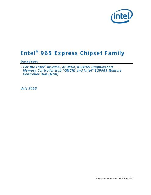
Introduction<br />
Figure 1-1. Intel ® Q<strong>965</strong>/G<strong>965</strong> <strong>Express</strong> <strong>Chipset</strong> System Block Diagram Example<br />
Display<br />
VGA<br />
Display<br />
Display<br />
Graphics<br />
Card<br />
USB* 2.0<br />
10 ports<br />
GPIO<br />
6 SATA* Ports<br />
Intel ® High<br />
Definition Audio<br />
CODECs<br />
SPI Flash<br />
ADD2 or<br />
MEC<br />
533/800/1066 MHz FSB<br />
Analog<br />
Display<br />
SDVO<br />
OR<br />
PCI <strong>Express</strong>*<br />
x16 Graphics<br />
SPI<br />
Flash BIOS<br />
TPM<br />
DMI<br />
Interface<br />
Processor<br />
Intel ® Q<strong>965</strong>/G<strong>965</strong> <strong>Express</strong> <strong>Chipset</strong><br />
Channel A<br />
GMCH DDR2<br />
Controller<br />
Link<br />
Intel ® ICH8 <strong>Family</strong><br />
LPC Interface<br />
Channel B<br />
PCI Bus<br />
System Memory<br />
<strong>Datasheet</strong> 21<br />
LCI<br />
Super I/O<br />
DDR2<br />
Power Management<br />
Clock Generation<br />
SST<br />
(Fan Speed Control)<br />
PCIe Bus<br />
SMBus 2.0/I 2 C<br />
Nineveh LAN<br />
5w/LAN or 6<br />
PCIe SLots<br />
4 PCI Masters<br />
Sys_Blk_Q995-G<strong>965</strong>
Figure 1-2. Intel ® Q963 <strong>Express</strong> <strong>Chipset</strong> System Block Diagram Example<br />
VGA<br />
Display ADD2<br />
Display<br />
USB* 2.0<br />
10 ports<br />
GPIO<br />
6 SATA* Ports<br />
Intel ® High<br />
Definition Audio<br />
CODECs<br />
SPI Flash<br />
533/800/1066 MHz FSB<br />
Analog<br />
Display<br />
SDVO<br />
SPI<br />
Flash BIOS<br />
TPM<br />
DMI<br />
Interface<br />
Processor<br />
Intel ® Q963 <strong>Express</strong> <strong>Chipset</strong><br />
Channel A<br />
GMCH DDR2<br />
Controller<br />
Link<br />
Intel ® ICH8 <strong>Family</strong><br />
LPC Interface<br />
Channel B<br />
PCI Bus<br />
Introduction<br />
System Memory<br />
22 <strong>Datasheet</strong><br />
LCI<br />
Super I/O<br />
DDR2<br />
Power Management<br />
Clock Generation<br />
SST<br />
(Fan Speed Control)<br />
PCIe Bus<br />
SMBus 2.0/I 2 C<br />
Nineveh LAN<br />
5w/LAN or 6<br />
PCIe SLots<br />
4 PCI Masters<br />
Sys_Blk_G995
Introduction<br />
Figure 1-3. Intel ® P<strong>965</strong> <strong>Express</strong> <strong>Chipset</strong> System Block Diagram Example<br />
Display<br />
Graphics<br />
Card<br />
USB* 2.0<br />
10 ports<br />
GPIO<br />
6 SATA* Ports<br />
Intel ® High<br />
Definition Audio<br />
CODECs<br />
SPI Flash<br />
533/800/1066 MHz FSB<br />
PCI <strong>Express</strong>*<br />
x16 Graphics<br />
SPI<br />
Flash BIOS<br />
TPM<br />
DMI<br />
Interface<br />
Processor<br />
Intel ® P<strong>965</strong> <strong>Express</strong> <strong>Chipset</strong><br />
Channel A<br />
MCH DDR2<br />
Controller<br />
Link<br />
Intel ® ICH8 <strong>Family</strong><br />
LPC Interface<br />
Channel B<br />
PCI Bus<br />
System Memory<br />
<strong>Datasheet</strong> 23<br />
LCI<br />
Super I/O<br />
DDR2<br />
Power Management<br />
Clock Generation<br />
SST<br />
(Fan Speed Control)<br />
PCIe Bus<br />
SMBus 2.0/I 2 C<br />
Nineveh LAN<br />
5w/LAN or 6<br />
PCIe SLots<br />
4 PCI Masters<br />
Sys_Blk_P<strong>965</strong>
1.1 Terminology<br />
Term Description<br />
Introduction<br />
ADD Card Advanced Digital Display Card. Provides digital display options for an Intel<br />
Graphics Controller that supports ADD cards (have DVOs multiplexed with<br />
AGP interface). Keyed like an AGP 4x card and plugs into an AGP connector.<br />
Will not work with an Intel Graphics Controller that implements Intel ® SDVO.<br />
ADD2 Card Advanced Digital Display Card – 2 nd Generation. Provides digital display<br />
options for an Intel graphics controller that supports ADD2 cards. Plugs into<br />
an x16 PCI <strong>Express</strong>* connector but utilizes the multiplexed SDVO interface.<br />
Will not work with an Intel Graphics Controller that supports Intel ® DVO and<br />
ADD cards.<br />
Media<br />
Media Expansion Card –. Provides digital display options for an Intel<br />
Expansion<br />
Graphics Controller that supports MEC cards. Plugs into an x16 PCI <strong>Express</strong><br />
Card<br />
(MEC)<br />
connector but utilizes the multiplexed SDVO interface. Adds Video In<br />
capabilities to platform. Will not work with an Intel Graphics Controller that<br />
supports DVO and ADD cards. Will function as an ADD2 card in an ADD2<br />
supported system, but Video In capabilities will not work.<br />
Core The internal base logic in the (G)MCH<br />
Processor Refers to the Intel ® Core2 Duo desktop processor, Intel ® Pentium ® D<br />
processor, and Intel ® Pentium ® 4 processor.<br />
CRT Cathode Ray Tube<br />
DBI Dynamic Bus Inversion<br />
DDR2 A second generation Double Data Rate SDRAM memory technology<br />
DMI (G)MCH-Intel ® ICH8 Direct Media Interface<br />
DVI Digital Video Interface. Specification that defines the connector and interface<br />
for digital displays.<br />
FSB Front Side Bus, synonymous with Host or processor bus<br />
Full Reset Full reset is when PWROK is de-asserted. Warm reset is when both RSTIN#<br />
and PWROK are asserted.<br />
GMCH Graphics Memory Controller Hub component that contains the processor<br />
interface, DRAM controller, internal graphics controller (IGD), and graphics<br />
interfaces. It communicates with the I/O controller hub (Intel ® ICH8*) over<br />
the DMI interconnect and Control interfaces.<br />
(G)MCH Term used when referring to both GMCH and MCH components.<br />
HDMI High Definition Multimedia Interface – HDMI supports standard, enhanced,<br />
or high-definition video, plus multi-channel digital audio on a single cable. It<br />
transmits all ATSC HDTV standards and supports 8-channel digital audio,<br />
with bandwidth to spare for future requirements and enhancements<br />
(additional details available through http://www.hdmi.org/)<br />
Host This term is used synonymously with processor<br />
INTx An interrupt request signal where X stands for interrupts A, B, C and D<br />
IOQ In Order Queue<br />
Intel ® AMT Intel ® Active Management Technology. Second generation system<br />
management technology.<br />
24 <strong>Datasheet</strong>
Introduction<br />
Term Description<br />
Intel ® ICH8 Eighth generation I/O Controller Hub component that contains additional<br />
functionality compared to previous Intel ® ICHs, The Intel ® I/O Controller<br />
Hub component contains the primary PCI interface, LPC interface, USB2,<br />
SATA, and other I/O functions. It communicates with the (G)MCH over a<br />
proprietary interconnect called DMI.<br />
IGD Internal Graphics Device<br />
LCD Liquid Crystal Display<br />
LVDS Low Voltage Differential Signaling. A high speed, low power data<br />
transmission standard used for display connections to LCD panels.<br />
OOQ Out of Order Queuing:<br />
MCH Memory Controller Hub that contains a host interface, DRAM controller, and<br />
DMI/Controller interface connections to the ICH8. In this document MCH<br />
refers to the 82P<strong>965</strong> MCH.<br />
ME Manageability engine for BTS ’06 Intel ® AMT<br />
MSI Message Signaled Interrupt. A transaction initiated outside the host,<br />
conveying interrupt information to the receiving agent through the same<br />
path that normally carries read and write commands.<br />
PCI <strong>Express</strong>* Third Generation Input Output (PCI <strong>Express</strong>) Graphics Attach called PCI<br />
<strong>Express</strong> Graphics. A high-speed serial interface whose configuration is<br />
software compatible with the existing PCI specifications. The specific PCI<br />
<strong>Express</strong> implementation intended for connecting the (G)MCH to an external<br />
Graphics Controller is an x16 link and replaces AGP.<br />
Primary PCI The physical PCI bus that is driven directly by the Intel ® ICH8 component.<br />
Communication between Primary PCI and the (G)MCH occurs over DMI. Note<br />
that the Primary PCI bus is not PCI Bus 0 from a configuration standpoint.<br />
SCI System Control Interrupt. Used in ACPI protocol.<br />
SDVO Serial Digital Video Out (SDVO). Digital display channel that serially<br />
transmits digital display data to an external SDVO device. The SDVO device<br />
accepts this serialized format and then translates the data into the<br />
appropriate display format (i.e. TMDS, LVDS, and TV-Out). This interface is<br />
not electrically compatible with the previous digital display channel - DVO.<br />
For the 82Q<strong>965</strong>, 82G<strong>965</strong>, the SDVO ports are multiplexed on a portion of<br />
the x16 graphics PCI <strong>Express</strong> interface.<br />
SDVO Device Third party codec that utilizes SDVO as an input. May have a variety of<br />
output formats, including DVI, LVDS, HDMI, TV-out, etc.<br />
SERR An indication that an unrecoverable error has occurred on an I/O bus.<br />
SMI System Management Interrupt. Used to indicate any of several system<br />
conditions such as thermal sensor events, throttling activated, access to<br />
System Management RAM, chassis open, or other system state related<br />
activity.<br />
Rank A unit of DRAM corresponding to eight x8 SDRAM devices in parallel or four<br />
x16 SDRAM devices in parallel, ignoring ECC. These devices are usually, but<br />
not always, mounted on a single side of a DIMM.<br />
TMDS Transition Minimized Differential Signaling. Signaling interface from Silicon<br />
Image that is used in DVI and HDMI.<br />
VCO Voltage Controlled Oscillator<br />
UMA Unified Memory Architecture. Describes an IGD using system memory for its<br />
frame buffers.<br />
<strong>Datasheet</strong> 25
1.2 Reference Documents<br />
Document Name Location<br />
Introduction<br />
Intel ® <strong>965</strong> <strong>Express</strong> <strong>Chipset</strong> <strong>Family</strong> Specification Update www.intel.com/design/c<br />
hipsets/specupdt/31305<br />
4.htm<br />
Intel ® <strong>965</strong> <strong>Express</strong> <strong>Chipset</strong> <strong>Family</strong> Thermal Mechanical Design<br />
Guide.<br />
Intel ® Pentium ® D Processor 900 Sequence, Intel ® Pentium ®<br />
Processor Extreme Edition, and Intel ® Pentium ® 4 Processor<br />
Thermal and Mechanical Design Guidelines<br />
Intel ® Core2 Duo Desktop Processor E6000 Sequence Thermal<br />
and Mechanical Design Guidelines<br />
Intel ® I/O Controller Hub 8 (ICH8) <strong>Family</strong> Thermal Mechanical<br />
Design Guide.<br />
Advanced Configuration and Power Interface Specification,<br />
Version 2.0<br />
Advanced Configuration and Power Interface Specification,<br />
Version 1.0b<br />
www.intel.com/design/c<br />
hipsets/designex/31305<br />
5.htm<br />
http://intel.com/design/<br />
pentiumXE/designex/<br />
306830.htm<br />
313685<br />
www.intel.com/design/c<br />
hipsets/designex/31305<br />
8.htm<br />
http://www.acpi.info/<br />
http://www.acpi.info/<br />
The PCI Local Bus Specification, Version 2.3 http://www.pcisig.com/s<br />
pecifications<br />
PCI <strong>Express</strong>* Specification, Version 1.1 http://www.pcisig.com/s<br />
pecifications<br />
1.3 (G)MCH Overview<br />
The (G)MCH is designed for use with the Intel Core2 Duo desktop processor,<br />
Pentium D processor and Pentium 4 processor desktop platforms. The role of a<br />
(G)MCH in a system is to manage the flow of information between its four interfaces:<br />
the processor interface (FSB), the System Memory interface (DRAM controller), the<br />
External Graphics interface (82Q<strong>965</strong>, 82G<strong>965</strong>, 82P<strong>965</strong> (G)MCH only), and the I/O<br />
Controller through the DMI interface. This includes arbitrating between the four<br />
interfaces when each initiates transactions. The processor interface supports the<br />
Pentium 4 processor subset of the Extended Mode of the Scalable Bus Protocol. The<br />
(G)MCH is optimized for the Intel ® Pentium ® 4 and Pentium D processor family in an<br />
LGA775 socket. The (G)MCH supports one or two channels of DDR2 SDRAM. It also<br />
supports the PCI <strong>Express</strong> based external graphics attach (82Q<strong>965</strong>, 82Q963), 82G<strong>965</strong><br />
GMCH only). The Q<strong>965</strong>/Q963/G<strong>965</strong>/P<strong>965</strong> express chipset platforms support the eighth<br />
generation I/O Controller Hub (Intel ICH8) to provide a multitude of I/O related<br />
features.<br />
26 <strong>Datasheet</strong>
Introduction<br />
1.3.1 Host Interface<br />
The (G)MCH can use a single LGA775 socket processor. The (G)MCH supports a FSB<br />
frequency of 533/800/1066 MHz using a scalable FSB Vcc_CPU. It supports 36-bit host<br />
addressing, decoding up to 8 GB of the processor’s memory address space. Hostinitiated<br />
I/O cycles are decoded to PCI <strong>Express</strong> (82Q<strong>965</strong>, 82G<strong>965</strong>, 82P<strong>965</strong> (G)MCH<br />
only), DMI, or the (G)MCH configuration space. Host-initiated memory cycles are<br />
decoded to PCI <strong>Express</strong>, DMI or system memory. PCI <strong>Express</strong> device accesses<br />
(82Q<strong>965</strong>, 82G<strong>965</strong>, 82P<strong>965</strong> (G)MCH only) to non-cacheable system memory are not<br />
snooped on the host bus. Memory accesses initiated from PCI <strong>Express</strong> using PCI<br />
semantics and from DMI to system SDRAM will be snooped on the host bus.<br />
Capabilities of the Processor/Host Interface (FSB) interface include:<br />
• Supports a single the Intel Core2 Duo desktop processor, Pentium D processor<br />
and Pentium 4 processor. Processors supported include: Intel ® Pentium ® D<br />
processor 900 sequence, Intel ® Pentium ® processor Extreme Edition <strong>965</strong>, 955,<br />
Intel ® Pentium ® 4 processor 6x1 sequence in an LGA775 package.<br />
• Supports the Pentium 4 and Pentium D processor subset of the Extended Mode<br />
Scaleable Bus Protocol. The primary enhancements over the Compatible Mode P6<br />
bus protocol are:<br />
⎯ Source synchronous double-pumped (2x) Address<br />
⎯ Source synchronous quad-pumped (4x) Data<br />
• Supports Pentium 4 processor and Pentium D processor FSB interrupt delivery<br />
• Supports Pentium 4 processor and Pentium D processor Front Side Bus (FSB) at<br />
the following frequency ranges:<br />
⎯ 533 MT/s (133 MHz)<br />
⎯ 800 MT/s (200 MHz)<br />
⎯ 1066 MT/s (266 MHz)<br />
• Supports Hyper-Threading Technology (HT Technology)<br />
• Supports FSB Dynamic Bus Inversion (DBI)<br />
• Supports 36-bit host bus addressing, allowing the processor to access the entire<br />
64 GB of the (G)MCH’s memory address space<br />
• Has a 12-deep In-Order Queue to support up to twelve outstanding pipelined<br />
address requests on the host bus<br />
• Has a 1-deep Defer Queue<br />
• Uses GTL+ bus driver with integrated GTL termination resistors<br />
• Supports a Cache Line Size of 64 bytes<br />
<strong>Datasheet</strong> 27
1.3.2 System Memory Interface<br />
Introduction<br />
The (G)MCH integrates a system memory DDR2 controller with two, 64-bit wide<br />
interfaces.<br />
Only Double Data Rate (DDR2) memory is supported; consequently, the buffers<br />
support only SSTL_1.8 V signal interfaces. The memory controller interface is fully<br />
configurable through a set of control registers.<br />
Capabilities of the system memory interface include:<br />
• Enhanced scheduling and out of order accesses using Intel ® Fast Memory Access<br />
• The (G)MCH System Memory Controller directly supports one or two channels of<br />
memory (each channel consisting of 64 data lines)<br />
⎯ The memory channels are asymmetric: "Flex Memory" channels are assigned<br />
addresses serially. Channel B addresses are assigned after all Channel A<br />
addresses<br />
⎯ The memory channels are interleaved: Addresses are bounced between the<br />
channels after each cache line (64-B boundary)<br />
• Supports DDR2 memory DIMM frequencies of 533, 667 and 800 MHz. The speed<br />
used in all channels is the speed of the slowest DIMM in the system<br />
• I/O Voltage of 1.8 V for DDR2<br />
• Supports only unbuffered DIMMs<br />
• Supports maximum memory bandwidth of 6.4 GB/s in single-channel or dualchannel<br />
asymmetric mode, or 12.8 GB/s in dual-channel interleaved mode<br />
assuming DDR2 800MHz<br />
• Supports 256-Mb, 512-Mb, and 1-Gb technologies for x8 and x16 devices (DDR2<br />
800MHz 1Gb technology not supported)<br />
• Supports four banks for all DDR2 devices up to 512-Mbit density. Supports eight<br />
banks for 1-Gbit DDR2 devices<br />
• Using 256 Mb technologies, the smallest memory capacity possible is 128 MB,<br />
assuming Single-Channel Mode. (8 K rows * 512 columns * 1 cell/(row * column)<br />
* 16 b/cell * 4 banks/devices * 4 devices/DIMM-side * 1 DIMM-side/channel * 1<br />
channel * 1 B/8 b * 1 M/1024 K = 128 MB)<br />
• By using 1 Gb technology (DDR2 800MHz 1 Gb technology is not supported) in<br />
Dual Channel Interleaved Mode, the largest memory capacity possible is 8 GB. (16<br />
K rows * 1 K columns * 1 cell/(row * column) * 8 b/cell * 8 banks/device * 8<br />
devices/DIMM-side * 4 DIMM-sides/channel * 2 channels * 1 B/8 b * 1 G/1024 M<br />
* 1 M/(K*K) = 8 GB)<br />
• Maximum DRAM address decode space is 8 GB (assuming 36-bit addressing)<br />
• Supports up to 32 simultaneous open pages per channel (assuming 4 ranks of 8<br />
bank devices)<br />
• Supports opportunistic refresh scheme<br />
• Supports Partial Writes to memory using Data Mask (DM) signals<br />
• Supports page sizes of 4 KB, 8 KB and 16 KB<br />
• Supports a burst length of 8 for single-channel and dual-channel interleaved and<br />
asymmetric operating modes<br />
• Improved flexible memory architecture<br />
28 <strong>Datasheet</strong>
Introduction<br />
1.3.3 Direct Media Interface (DMI)<br />
Direct Media Interface (DMI) is the chip-to-chip connection between the (G)MCH and<br />
ICH8. This high-speed interface integrates advanced priority-based servicing allowing<br />
for concurrent traffic and true isochronous transfer capabilities. Base functionality is<br />
completely software transparent permitting current and legacy software to operate<br />
normally.<br />
To provide for true isochronous transfers and configurable Quality of Service (QoS)<br />
transactions, the ICH8 supports two virtual channels on DMI: VC0 and VC1. These two<br />
channels provide a fixed arbitration scheme where VC1 is always the highest priority.<br />
VC0 is the default conduit of traffic for DMI and is always enabled. VC1 must be<br />
specifically enabled and configured at both ends of the DMI link (i.e., the ICH8 and<br />
(G)MCH).<br />
• A chip-to-chip connection interface to Intel ICH8<br />
• 2 GB/s point-to-point DMI to ICH8 (1 GB/s each direction)<br />
• 100 MHz reference clock (shared with PCI <strong>Express</strong> Graphics Attach)<br />
• 32-bit downstream addressing<br />
• APIC and MSI interrupt messaging support. Will send Intel-defined “End Of<br />
Interrupt” broadcast message when initiated by the processor.<br />
• Message Signaled Interrupt (MSI) messages<br />
• SMI, SCI and SERR error indication<br />
• Legacy support for ISA regime protocol (PHOLD/PHOLDA) required for parallel port<br />
DMA, floppy drive, and LPC bus masters<br />
1.3.4 PCI <strong>Express</strong>* Interface (Intel ® 82Q<strong>965</strong>, 82G<strong>965</strong>, 82P<strong>965</strong><br />
(G)MCH Only)<br />
The (G)MCH contains one 16-lane (x16) PCI <strong>Express</strong> port intended for an external PCI<br />
<strong>Express</strong> graphics card. The PCI <strong>Express</strong> port is compliant to the PCI <strong>Express</strong>* Base<br />
Specification revision 1.1. The x16 port operates at a frequency of 2.5 Gb/s on each<br />
lane while employing 8b/10b encoding; the port supports a maximum theoretical<br />
bandwidth of 40 Gb/s in each direction. The 82Q<strong>965</strong> and 82G<strong>965</strong> GMCHs multiplex the<br />
PCI <strong>Express</strong> interface with the Intel ® SDVO ports.<br />
• One, 16-lane PCI <strong>Express</strong> port intended for graphics attach, compatible to the PCI<br />
<strong>Express</strong>* Base Specification revision 1.1a.<br />
• PCI <strong>Express</strong> frequency of 1.25 GHz resulting in 2.5 Gb/s each direction<br />
• Raw bit-rate on the data pins of 2.5 Gb/s, resulting in a real bandwidth per pair of<br />
250 MB/s given the 8b/10b encoding used to transmit data across this interface<br />
• Maximum theoretical realized bandwidth on the interface of 4 GB/s in each<br />
direction simultaneously, for an aggregate of 8 GB/s when x16.<br />
• PCI <strong>Express</strong>* Graphics Extended Configuration Space. The first 256 bytes of<br />
configuration space alias directly to the PCI Compatibility configuration space. The<br />
remaining portion of the fixed 4-KB block of memory-mapped space above that<br />
(starting at 100h) is known as extended configuration space.<br />
<strong>Datasheet</strong> 29
Introduction<br />
• PCI <strong>Express</strong> Enhanced Addressing Mechanism. Accessing the device configuration<br />
space in a flat memory mapped fashion.<br />
• Automatic discovery, negotiation, and training of link out of reset<br />
• Supports traditional PCI style traffic (asynchronous snooped, PCI ordering)<br />
• Supports traditional AGP style traffic (asynchronous non-snooped, PCI <strong>Express</strong>relaxed<br />
ordering)<br />
• Hierarchical PCI-compliant configuration mechanism for downstream devices (i.e.,<br />
normal PCI 2.3 Configuration space as a PCI-to-PCI bridge)<br />
• Supports “static” lane numbering reversal. This method of lane reversal is<br />
controlled by a Hardware Reset strap, and reverses both the receivers and<br />
transmitters for all lanes (e.g., TX[15]->TX[0], RX[15]->RX[0]). This method is<br />
transparent to all external devices and is different than lane reversal as defined in<br />
the PCI <strong>Express</strong> Specification. In particular, link initialization is not affected by<br />
static lane reversal.<br />
1.3.5 Intel ® Active Management Technology (Intel ® AMT)<br />
(Intel ® 82Q<strong>965</strong> GMCH Only)<br />
Intel ® AMT combines highly-available OOB remote management and network<br />
protection into an OS-independent and tamper-resistant solution to help<br />
address company IT department top issues of network protection, asset<br />
management, and system reliability.<br />
• Hardware and software asset management<br />
• Provide OOB diagnostics<br />
• Network protection with NOC filters and agent presence<br />
• Integrated hardware and software platform solution<br />
Intel ® AMT integrates advanced manageability features into hardware and<br />
firmware. Intel AMT extends the capabilities of existing management<br />
solutions by enabling system and S/W asset information, remote diagnostics,<br />
recovery and network protection through the OOB (Out-Of-Band) channel<br />
(i.e., it is available even when the system is in a low-power “off” state or the<br />
operating system is hung).<br />
Intel ® Active Management Technology is only supported by the Q<strong>965</strong> <strong>Express</strong><br />
chipset.<br />
30 <strong>Datasheet</strong>
Introduction<br />
1.3.6 Alerting Standard Format (ASF) (Intel ® 82Q<strong>965</strong> and<br />
82Q963 GMCH Only)<br />
ASF is a specification that Intel and IBM developed jointly back in 1997 and<br />
updated in 1999. Alerting Standard Format (ASF) provides alerting<br />
capabilities (no event log - history must be stored on server) to notify IT of<br />
system problems over the network. ASF provides basic power-up/powerdown<br />
capabilities.<br />
An ASF design contains several required components (a list of components is<br />
provided later in this section), and Intel provides some (but not all) of them.<br />
Each OEM must (1) decide what features to support and what devices are<br />
required, (2) ensure that these devices meet the ASF specification, and (3)<br />
acquire/develop any software/hardware not provided by Intel.<br />
ASF can be supported by the Q<strong>965</strong> Q963 <strong>Express</strong> chipsets. For Q<strong>965</strong> <strong>Express</strong><br />
chipset platforms, only one manageability solution can be supported.<br />
1.3.7 Graphics Features (Intel ® 82Q<strong>965</strong>, 82Q963, 82G<strong>965</strong><br />
GMCH)<br />
The GMCH provides an integrated graphics device (IGD) delivering cost competitive<br />
3D, 2D and video capabilities. The GMCH contains an extensive set of instructions for<br />
3D operations, 2D operations, motion compensation, overlay, and display control. The<br />
GMCH’s video engines support video conferencing and other video applications. The<br />
GMCH uses a UMA configuration with up to 256 MB of DVMT for graphics memory. The<br />
GMCH also has the capability to support external graphics accelerators via the PCI<br />
<strong>Express</strong>* Graphics (PEG) port but cannot work concurrently with the integrated<br />
graphics device. High bandwidth access to data is provided through the system<br />
memory port.<br />
<strong>Datasheet</strong> 31
1.3.8 SDVO and Analog Display Features (Intel ® 82Q<strong>965</strong>,<br />
82Q963, 82G<strong>965</strong> GMCH Only)<br />
Introduction<br />
The GMCH provides interfaces to a progressive scan analog monitor and two SDVO<br />
ports (multiplexed with PCI <strong>Express</strong> x16 graphics port signals on the 82Q<strong>965</strong> and<br />
82G<strong>965</strong> GMCH) capable of driving an Advanced Digital Display (ADD2) card or Media<br />
Expansion card (82Q<strong>965</strong> and 82G<strong>965</strong> GMCH only). The digital display channels are<br />
capable of driving a variety of SDVO devices (e.g., TMDS, TV-Out). Note that SDVO<br />
only works with the Integrated Graphics Device (IGD). The Media Expansion card adds<br />
Video-in capabilities. The GMCH provides two multiplexed SDVO ports that are capable<br />
of driving up to a 270 MHz pixel clock each. When combined with a DVI compliant<br />
external device and connector, the GMCH has a high-speed interface to a digital<br />
display (e.g., flat panel or digital CRT).<br />
The GMCH SDVO ports can each support a single-channel SDVO device. If both ports<br />
are active in single-channel mode, they can have different display timing and data.<br />
The GMCH is compliant with DVI Specification 1.0. Capabilities of the SDVO and<br />
Analog Display interfaces include:<br />
• SDVO Support<br />
⎯ SDVO ports in either single/single-combined or dual operation modes<br />
supported<br />
⎯ 3x3 Built In full panel scalar<br />
⎯ 180 degree Hardware screen rotation<br />
⎯ Multiplexed Digital Display Channels (Supported with ADD2 Card)<br />
⎯ Two channels multiplexed with PCI <strong>Express</strong>* Graphics port<br />
⎯ 270 MHz dot clock on each 12-bit interface<br />
⎯ Supports flat panels up to 2048x1536 @ 60 Hz or digital CRT/HDTV at<br />
1920x1080 @ 85 Hz<br />
⎯ Supports Hot-Plug and Display<br />
⎯ Supports TMDS transmitters or TV-out encoders<br />
⎯ ADD2/Media Expansion card use PCI <strong>Express</strong> Graphics x16 connector<br />
• Analog Display Support<br />
⎯ 400 MHz Integrated 24-bit RAMDAC<br />
⎯ Up to 2048x1536 @ 75 Hz refresh<br />
⎯ Hardware Color Cursor Support<br />
⎯ DDC2B Compliant Interface<br />
• Dual Independent Display options with digital display<br />
32 <strong>Datasheet</strong>
Introduction<br />
1.3.9 (G)MCH Clocking<br />
• Differential Host clock of 133/200/266 MHz (HCLKP/HCLKN). These clock<br />
frequencies support transfer rates of 533/800/1066 MT/s. The Host PLL generates<br />
2x, 4x, and 8x versions of the host clock for internal optimizations.<br />
• <strong>Chipset</strong> core clock synchronized to host clock<br />
• Internal and external memory clocks of 266 MHz, 333 MHz, and 400 MHz<br />
generated from one of two (G)MCH PLLs that use the host clock as a reference.<br />
This includes 2x and 4x for internal optimizations.<br />
• The PCI <strong>Express</strong>* PLL of 100 MHz. This serial reference clock (GCLKP/GCLKN)<br />
generates the PCI <strong>Express</strong> core clock of 250 MHz (82Q<strong>965</strong>, 82G<strong>965</strong>, 82P<strong>965</strong><br />
(G)MCH only).<br />
• Display timings are generated from display PLLs that use a 96 MHz differential<br />
non-spread spectrum clock as a reference. Display PLLs can also use the<br />
SDVO_TVCLKIN[+/-] from an SDVO device as a reference. (82Q<strong>965</strong>, 82Q963,<br />
82G<strong>965</strong> GMCH Only)<br />
• All of the above clocks are capable of tolerating Spread Spectrum clocking as<br />
defined in the Clock Generator specification.<br />
• Host, Memory, and PCI <strong>Express</strong> Graphics PLLs, and all associated internal clocks<br />
are disabled until PWROK is asserted.<br />
1.3.10 Thermal Sensor<br />
The (G)MCH Thermal Sensor support includes:<br />
• Catastrophic Trip Point support for emergency clock gating for the (G)MCH at<br />
118 °C<br />
• Hot Trip Point support for SMI generation between 85 °C and 105 °C<br />
1.3.11 Power Management<br />
(G)MCH Power Management support includes:<br />
• PC99 suspend to DRAM support (“STR”, mapped to ACPI state S3)<br />
• SMRAM space remapping to A0000h (128 KB)<br />
• Supports extended SMRAM space above 256 MB, additional 1-MB TSEG from<br />
the Base of graphics stolen memory (BSM) when enabled, and cacheable<br />
(cacheability controlled by processor)<br />
• ACPI Rev 1.0 compatible power management<br />
• Supports processor states: C0 and C1<br />
• Supports System states: S0, S1D, S3, S4, and S5<br />
• Supports processor Thermal Management 2 (TM2)<br />
<strong>Datasheet</strong> 33<br />
§
Introduction<br />
34 <strong>Datasheet</strong>
Signal Description<br />
2 Signal Description<br />
This section provides a detailed description of (G)MCH signals. The signals are<br />
arranged in functional groups according to their associated interface (see Figure 2-1).<br />
Table 2-1 lists the notations used to describe the signal type.<br />
Table 2-1. Signal Terminology<br />
Term Description<br />
PCI <strong>Express</strong>* PCI-<strong>Express</strong> interface signals. These signals are compatible with PCI<br />
<strong>Express</strong> 1.1 Signaling Environment AC Specifications and are AC coupled.<br />
The buffers are not 3.3 V tolerant. Differential voltage spec = (|D+ - D-|) * 2<br />
= 1.2Vmax. Single-ended maximum = 1.25 V.<br />
Single-ended minimum = 0 V.<br />
DMI Direct Media Interface signals. These signals are compatible with PCI<br />
<strong>Express</strong> 1.0 Signaling Environment AC Specifications, but are DC coupled.<br />
The buffers are not 3.3 V tolerant. Differential voltage spec = (|D+ - D-|) * 2<br />
= 1.2Vmax. Single-ended maximum = 1.25 V.<br />
Single-ended minimum = 0 V.<br />
CMOS CMOS buffers. 1.5 V tolerant.<br />
COD CMOS Open Drain buffers. 3.3 V tolerant.<br />
HCSL Host Clock Signal Level buffers. Current mode differential pair.<br />
Differential typical swing = (|D+ - D-|) * 2 = 1.4V. Single ended input<br />
tolerant from -0.35 V to 1.2 V. Typical crossing voltage 0.35 V.<br />
HVCMOS High Voltage CMOS buffers. 3.3 V tolerant.<br />
HVIN High Voltage CMOS input-only buffers. 3.3 V tolerant.<br />
SSTL-1.8 Stub Series Termination Logic. These are 1.8 V output capable buffers.<br />
1.8 V tolerant.<br />
A Analog reference or output. May be used as a threshold voltage or for<br />
buffer compensation.<br />
GTL+ Gunning Transceiver Logic signaling technology. Implements a voltage<br />
level as defined by VTT of 1.2 V.<br />
<strong>Datasheet</strong> 35
Figure 2-1. Signal Information Diagram<br />
HA[35:3]#<br />
HD[63:0]#<br />
HADS#<br />
HBNR#<br />
HBPRI#<br />
HDBSY#<br />
HDEFER#<br />
HDRDY#<br />
HEDRDY#<br />
HHIT#<br />
HHITM#<br />
HLOCK#<br />
HREQ[4:0]#<br />
HPCREQ#<br />
HTRDY#<br />
HRS[2:0]#<br />
HCPURST#<br />
HBREQ0#<br />
HDINV[3:0]#<br />
HADSTB[1:0]#<br />
HDSTBP[3:0]#, HDSTBN[3:0]#<br />
BSEL[2:0]<br />
HRCOMP<br />
HSCOMP<br />
HSWING<br />
HDVREF<br />
HACCVREF<br />
SCS_A[3:0]#<br />
SMA_A[14:0]<br />
SBS_A[2:0]<br />
SRAS_A#<br />
SCAS_A#<br />
SWE_A#<br />
SDQ_A[63:0]<br />
SDM_A[7:0]<br />
SDQS_A[7:0], SDQS_A[7:0]#<br />
SCKE_A[3:0]<br />
SCLK_A[5:0], SCLK_A[5:0]#<br />
SODT_A[3:0]<br />
SCS_B[3:0]#<br />
SMA_B[14:0]<br />
SBS_B[2:0]<br />
SRAS_B#<br />
SCAS_B#<br />
SWE_B#<br />
SDQ_B[63:0]<br />
SDM_B[7:0]<br />
SDQS_B[7:0], SDQS_B[7:0]#<br />
SCKE_B[3:0]<br />
SCLK_B[5:0], SCLK_B[5:0]#<br />
SODT_B[3:0]<br />
SRCOMP[3:0]<br />
SVREF<br />
SMRCOMPVOL<br />
SMRCOMPVOH<br />
Processor<br />
System<br />
Bus<br />
Interface<br />
System<br />
Memory<br />
DDR2<br />
Channel<br />
A<br />
System<br />
Memory<br />
DDR2<br />
Channel<br />
B<br />
System<br />
Memory<br />
DDR2 Ref./<br />
Comp.<br />
Analog<br />
Display<br />
Intel ®<br />
SDVO<br />
Device<br />
Interface 1<br />
PCI<br />
<strong>Express</strong>*<br />
x16<br />
Graphics<br />
Port<br />
Clocks,<br />
Reset, and<br />
Misc.<br />
Controller<br />
Link<br />
Direct<br />
Media<br />
Interface<br />
Voltage<br />
Reference,<br />
and Power<br />
HSYNC<br />
VSYNC<br />
RED, RED#<br />
GREEN, GREEN#<br />
BLUE, BLUE#<br />
REFSET<br />
DDC_CLK<br />
DDC_DATA<br />
SDVOB_GREEN-, SDVOB_GREEN+<br />
SDVOB_BLUE-, SDVOB_BLUE+<br />
SDVOB_RED-, SDVOB_RED+<br />
SDVOB_CLK-, SDVOB_CLK+<br />
SDVOC_RED- / SDVOB_ALPHA-,<br />
SDVOC_RED+ / SDVOB_ALPHA+<br />
SDVOC_GREEN-, SDVOC_GREEN+<br />
SDVOC_BLUE-, SDVOC_BLUE+<br />
SDVOC_CLK-, SDVOC_CLK+<br />
SDVO_TVCLKIN-, SDVO_TVCLKIN+<br />
SDVOB_INT-, SDVOB_INT+<br />
SDVOC_INT-, SDVOC_INT+<br />
SDVO_FLDSTALL-, SDVO_FLDSTALL+<br />
SDVO_CTRLCLK<br />
SDVO_CTRLDATA<br />
EXP_RXN[15:0], EXP_RXP[15:0]<br />
EXP_TXN[15:0], EXP_TXP[15:0]<br />
EXP_COMPO<br />
EXP_COMPI<br />
HCLKP, HCLKN<br />
GCLKP, GCLKN<br />
DREFCLKN, DREFCLKP<br />
RSTIN#<br />
PWROK<br />
EXP_EN<br />
EXP_SLR<br />
ICH_SYNC#<br />
TEST[2:0]<br />
CL_DATA<br />
CL_CLK<br />
CL_VREF<br />
Cl_RST#<br />
CL_PWROK<br />
DMI_RXP[3:0], DMI_RXN[3:0]<br />
DMI_TXP[3:0], DMI_TXN[3:0]<br />
VCC<br />
VTT<br />
VCC_EXP<br />
VCCSM<br />
VCCSMCLK<br />
VCC3_3<br />
VCCA_EXPPLL<br />
VCCA_DPLLA<br />
VCCA_DPLLB<br />
VCCA_HPLL<br />
VCCA_MPLL<br />
VCCA_DAC<br />
VCCA_EXP<br />
VCCDQ_CRT<br />
VCC_CL<br />
VCC_CL_PLL<br />
VSS<br />
NOTE:<br />
1. SDVO signals on the 82<strong>965</strong>Q, 82<strong>965</strong>G GMCH are multiplexed with the PCI <strong>Express</strong> x16 Graphics Port signals.<br />
Signal Description<br />
Intel ®<br />
82<strong>965</strong>Q,<br />
82963Q,<br />
82<strong>965</strong>G<br />
GMCH Only<br />
36 <strong>Datasheet</strong><br />
Signal_Info<br />
Intel ®<br />
82<strong>965</strong>Q,<br />
82963Q,<br />
82<strong>965</strong>G<br />
GMCH<br />
Only<br />
Intel ®<br />
82<strong>965</strong>Q,<br />
82<strong>965</strong>G,<br />
82<strong>965</strong>P<br />
GMCH Only
Signal Description<br />
2.1 Host Interface Signals<br />
Note: Unless otherwise noted, the voltage level for all signals in this interface is tied to the<br />
termination voltage of the Host Bus (V TT).<br />
Signal Name Type Description<br />
HADS# I/O<br />
GTL+<br />
HBNR# I/O<br />
GTL+<br />
HBPRI# O<br />
GTL+<br />
HBREQ0# I/O<br />
GTL+<br />
HCPURST# O<br />
GTL+<br />
HDBSY# I/O<br />
GTL+<br />
HDEFER# O<br />
GTL+<br />
Address Strobe: The processor bus owner asserts HADS# to<br />
indicate the first of two cycles of a request phase. The (G)MCH<br />
can assert this signal for snoop cycles and interrupt messages.<br />
Block Next Request: This signal is used to block the current<br />
request bus owner from issuing new requests. This signal is<br />
used to dynamically control the processor bus pipeline depth.<br />
Priority Agent Bus Request: The (G)MCH is the only Priority<br />
Agent on the processor bus. It asserts this signal to obtain the<br />
ownership of the address bus. This signal has priority over<br />
symmetric bus requests and will cause the current symmetric<br />
owner to stop issuing new transactions unless the HLOCK#<br />
signal was asserted.<br />
Bus Request 0: The (G)MCH pulls the processor’s bus<br />
HBREQ0# signal low during HCPURST#. The processor samples<br />
this signal on the active-to-inactive transition of HCPURST#.<br />
The minimum setup time for this signal is 4 HCLKs. The<br />
minimum hold time is 2 HCLKs and the maximum hold time is<br />
20 HCLKs. HBREQ0# should be tri-stated after the hold time<br />
requirement has been satisfied.<br />
CPU Reset: The HCPURST# pin is an output from the (G)MCH.<br />
The (G)MCH asserts HCPURST# while RSTIN# is asserted and<br />
for approximately 1 ms after RSTIN# is de-asserted. The<br />
HCPURST# allows the processors to begin execution in a known<br />
state.<br />
Note that the Intel ® ICH8 must provide processor frequency<br />
select strap setup and hold times around HCPURST#. This<br />
requires strict synchronization between (G)MCH HCPURST# deassertion<br />
and the ICH8 driving the straps.<br />
Data Bus Busy: This signal is used by the data bus owner to<br />
hold the data bus for transfers requiring more than one cycle.<br />
Defer: This signal indicates that the (G)MCH will terminate the<br />
transaction currently being snooped with either a deferred<br />
response or with a retry response.<br />
<strong>Datasheet</strong> 37
Signal Name Type Description<br />
HDINV[3:0]# I/O<br />
GTL+<br />
HA[35:3]# I/O<br />
GTL+<br />
HADSTB[1:0]# I/O<br />
GTL+<br />
HD[63:0]# I/O<br />
HDSTBP[3:0]#<br />
HDSTBN[3:0]#<br />
GTL+<br />
I/O<br />
GTL+<br />
HHIT# I/O<br />
GTL+<br />
HHITM# I/O<br />
GTL+<br />
HLOCK# I/O<br />
GTL+<br />
Signal Description<br />
Dynamic Bus Inversion: These signals are driven along with<br />
the HD[63:0]# signals. They indicate if the associated signals<br />
are inverted. HDINV[3:0]# are asserted such that the number<br />
of data bits driven electrically low (low voltage) within the<br />
corresponding 16 bit group never exceeds 8.<br />
HDINVx# Data Bits<br />
HDINV3# HD[63:48]#<br />
HDINV2# HD[47:32]#<br />
HDINV1# HD[31:16]#<br />
HDINV0# HD[15:0]#<br />
Host Address Bus: HA[35:3]# connect to the processor<br />
address bus. During processor cycles, the HA[35:3]# are<br />
inputs. The (G)MCH drives HA[35:3]# during snoop cycles on<br />
behalf of DMI and PCI <strong>Express</strong>* Graphics initiators. HA[35:3]#<br />
are transferred at 2x rate.<br />
Host Address Strobe: HADSTB[1:0]# are source synchronous<br />
strobes used to transfer HA[35:3]# and HREQ[4:0] at the 2x<br />
transfer rate.<br />
Host Data: These signals are connected to the processor data<br />
bus. Data on HD[63:0] are transferred at 4x rate. Note that the<br />
data signals may be inverted on the processor bus, depending<br />
on the HDINV[3:0]# signals.<br />
Differential Host Data Strobes: These signals are differential<br />
source synchronous strobes used to transfer HD[63:0]# and<br />
HDINV[3:0]# at 4x transfer rate.<br />
These signals are not level sensitive. Data is captured on the<br />
falling edge of both strobes. Hence, they are pseudodifferential,<br />
and not true differential.<br />
Strobes Bits Data<br />
HDSTBP3#, HDSTBN3# HDINV3# HD[63:48]#<br />
HDSTBP2#, HDSTBN2# HDINV2# HD[47:32]#<br />
HDSTBP1#, HDSTBN1# HDINV1# HD[31:16]#<br />
HDSTBP0#, HDSTBN0# HDINV0# HD[15:0]#<br />
Hit: This signal indicates that a caching agent holds an<br />
unmodified version of the requested line. This signal is also<br />
driven in conjunction with HHITM# by the target to extend the<br />
snoop window.<br />
Hit Modified: This signal indicates that a caching agent holds a<br />
modified version of the requested line and that this agent<br />
assumes responsibility for providing the line. This signal is also<br />
driven in conjunction with HHIT# to extend the snoop window.<br />
Host Lock: All processor bus cycles sampled with the assertion<br />
of HLOCK# and HADS#, until the negation of HLOCK#, must be<br />
atomic (i.e., no DMI or PCI <strong>Express</strong>* Graphics accesses to<br />
system memory are allowed when HLOCK# is asserted by the<br />
processor).<br />
38 <strong>Datasheet</strong>
Signal Description<br />
Signal Name Type Description<br />
HREQ[4:0]# I/O<br />
GTL+<br />
HTRDY# O<br />
GTL+<br />
HRS[2:0]# O<br />
GTL+<br />
BSEL[2:0] I<br />
CMOS<br />
HRCOMP I/O<br />
CMOS<br />
HSCOMP I/O<br />
CMOS<br />
HSCOMP# I/O<br />
HSWING I<br />
HDVREF I<br />
HACCVREF I<br />
A<br />
A<br />
A<br />
A<br />
Host Request Command: These signals define the attributes<br />
of the request. HREQ[4:0]# are transferred at 2x rate. They<br />
are Asserted by the requesting agent during both halves of<br />
Request Phase. In the first half, the signals define the<br />
transaction type to a level of detail that is sufficient to begin a<br />
snoop request. In the second half, the signals carry additional<br />
information to define the complete transaction type.<br />
Host Target Ready: This signal indicates that the target of the<br />
processor transaction is able to enter the data transfer phase.<br />
Response Signals: These signals indicate the type of response<br />
according to the following:<br />
000 Idle state<br />
001 Retry response<br />
010 Deferred response<br />
011 Reserved (not driven by (G)MCH)<br />
100 Hard Failure (not driven by (G)MCH)<br />
101 No data response<br />
110 Implicit Writeback<br />
111 Normal data response<br />
Bus Speed Select: At the de-assertion of RSTIN#, the value<br />
sampled on these signals determine the expected frequency of<br />
the bus.<br />
Host RCOMP: This signal is used to calibrate the Host GTL+<br />
I/O buffers. This signal is powered by the Host Interface<br />
termination rail (VTT).<br />
Slew Rate Compensation: This signal is used for<br />
compensation for the Host Interface.<br />
Slew Rate Compensation: This signal is used for<br />
compensation for the Host Interface for falling edges.<br />
Host Voltage Swing: This signal provides the reference<br />
voltage used by FSB RCOMP circuits. HSWING is used for the<br />
signals handled by HRCOMP.<br />
Host Reference Voltage: This signal is the voltage input for<br />
the data signals of the Host GTL interface.<br />
Host Reference Voltage: This signal is used the voltage input<br />
for the Address signals of the Host GTL interface.<br />
<strong>Datasheet</strong> 39
2.2 DDR2 DRAM Channel A Interface<br />
Signal Name Type Description<br />
SCLK_A[5:0] O<br />
SSTL-1.8<br />
SCLK_A[5:0]# O<br />
SSTL-1.8<br />
SCS_A[3:0]# O<br />
SSTL-1.8<br />
SMA_A[14:0] O<br />
SSTL-1.8<br />
SBS_A[2:0] O<br />
SSTL-1.8<br />
SRAS_A# O<br />
SSTL-1.8<br />
SCAS_A# O<br />
SSTL-1.8<br />
SWE_A# O<br />
SSTL-1.8<br />
SDQ_A[63:0] I/O<br />
SSTL-1.8<br />
SDM_A[7:0] O<br />
SSTL-1.8<br />
SDQS_A[7:0] I/O<br />
SSTL-1.8<br />
SDQS_A[7:0]# I/O<br />
SSTL-1.8<br />
SCKE_A[3:0] O<br />
SSTL-1.8<br />
SODT_A[3:0] O<br />
SSTL-1.8<br />
Signal Description<br />
SDRAM Differential Clock: (3 per DIMM). SCLK_Ax and its<br />
complement, SCLK_Ax# make a differential clock pair output.<br />
The crossing of the positive edge of SCLK_Ax and the<br />
negative edge of its complement SCLK_Ax# are used to<br />
sample the command and control signals on the SDRAM.<br />
SDRAM Complementary Differential Clock: (3 per DIMM).<br />
These are the complementary differential DDR2 clock signals.<br />
Chip Select: (1 per Rank) These signals select particular<br />
SDRAM components during the active state. There is one chip<br />
select for each SDRAM rank.<br />
Memory Address: These signals are used to provide the<br />
multiplexed row and column address to the SDRAM.<br />
Bank Select: These signals define which banks are selected<br />
within each SDRAM rank.<br />
DDR2: 1-Gb technology uses 8 banks.<br />
Row Address Strobe: This signal is used with SCAS_A# and<br />
SWE_A# (along with SCS_Ax#) to define the SDRAM<br />
commands.<br />
Column Address Strobe: This signal is used with SRAS_A#<br />
and SWE_A# (along with SCS_Ax#) to define the SDRAM<br />
commands.<br />
Write Enable: This signal is used with SCAS_A# and<br />
SRAS_A# (along with SCS_Ax#) to define the SDRAM<br />
commands.<br />
Data Lines: SDQ_Ax signals interface to the SDRAM data<br />
bus.<br />
Data Mask: When activated during writes, the corresponding<br />
data groups in the SDRAM are masked. There is one SDM_Ax<br />
bit for every data byte lane.<br />
Data Strobes: For DDR2, SDQS_Ax, and its complement<br />
SDQS_Ax# make up a differential strobe pair. The data is<br />
captured at the crossing point of SDQS_Ax and its<br />
complement SDQS_Ax# during read and write transactions.<br />
Data Strobe Complements: These are the complementary<br />
DDR2 strobe signals.<br />
Clock Enable: (1 per Rank). SCKE_Ax is used to initialize the<br />
SDRAMs during power-up, to power-down SDRAM ranks, and<br />
to place all SDRAM ranks into and out of self-refresh during<br />
Suspend-to-RAM.<br />
On Die Termination: SODT_A[3:0] are active On-die<br />
termination control signals for DDR2 devices.<br />
40 <strong>Datasheet</strong>
Signal Description<br />
2.3 DDR2 DRAM Channel B Interface<br />
Signal Name Type Description<br />
SCLK_B[5:0] O<br />
SSTL-1.8<br />
SCLK_B[5:0]# O<br />
SSTL-1.8<br />
SCS_B[3:0]# O<br />
SSTL-1.8<br />
SMA_B[14:0] O<br />
SSTL-1.8<br />
SBS_B[2:0] O<br />
SSTL-1.8<br />
SRAS_B# O<br />
SSTL-1.8<br />
SCAS_B# O<br />
SSTL-1.8<br />
SWE_B# O<br />
SSTL-1.8<br />
SDQ_B[63:0] I/O<br />
SSTL-1.8<br />
SDM_B[7:0] O<br />
SSTL-1.8<br />
SDQS_B[7:0] I/O<br />
SSTL-1.8<br />
SDQS_B[7:0]# I/O<br />
SSTL-1.8<br />
SCKE_B[3:0] O<br />
SSTL-1.8<br />
SODT_B[3:0] O<br />
SSTL-1.8<br />
SDRAM Differential Clock: (3 per DIMM). SCLK_Bx and its<br />
complement, SCLK_Bx#, make a differential clock pair<br />
output. The crossing of the positive edge of SCLK_Bx and<br />
the negative edge of its complement SCLK_Bx# are used to<br />
sample the command and control signals on the SDRAM.<br />
SDRAM Complementary Differential Clock: (3 per<br />
DIMM). These are the complementary differential DDR2<br />
clock signals.<br />
Chip Select: (1 per Rank) These signals select particular<br />
SDRAM components during the active state. There is one<br />
chip select for each SDRAM rank<br />
Memory Address: These signals are used to provide the<br />
multiplexed row and column address to the SDRAM.<br />
Bank Select: These signals define which banks are selected<br />
within each SDRAM rank<br />
DDR2: 1-Gb technology uses 8 banks.<br />
Row Address Strobe: This signal is used with SCAS_B#<br />
and SWE_B# (along with SCS_Bx#) to define the SDRAM<br />
commands<br />
Column Address Strobe: This signal is used with<br />
SRAS_B# and SWE_B# (along with SCS_Bx#) to define the<br />
SDRAM commands.<br />
Write Enable: This signal is used with SCAS_B# and<br />
SRAS_B# (along with SCS_Bx#) to define the SDRAM<br />
commands.<br />
Data Lines: SDQ_Bx signals interface to the SDRAM data<br />
bus.<br />
Data Mask: When activated during writes, the<br />
corresponding data groups in the SDRAM are masked. There<br />
is one SBDM_Bx for every data byte lane.<br />
Data Strobes: For DDR2, SDQS_Bx, and its complement<br />
,SDQS_Bx#, make up a differential strobe pair. The data is<br />
captured at the crossing point of SDQS_Bx and its<br />
complement SDQS_Bx# during read and write transactions.<br />
Data Strobe Complements: These are the complementary<br />
DDR2 strobe signals.<br />
Clock Enable: (1 per Rank). SCKE_Bx is used to initialize<br />
the SDRAMs during power-up, to power-down SDRAM ranks,<br />
and to place all SDRAM ranks into and out of self-refresh<br />
during Suspend-to-RAM.<br />
On Die Termination: SODT_B[3:0] are active On-die<br />
termination control signals for DDR2 devices.<br />
<strong>Datasheet</strong> 41
2.4 DDR2 DRAM Reference and Compensation<br />
Signal Name Type Description<br />
SRCOMP[3:0] I<br />
SVREF I<br />
SMRCOMPVOL I<br />
SMRCOMPVOH I<br />
A<br />
A<br />
A<br />
A<br />
System Memory RCOMP:<br />
Signal Description<br />
SDRAM Reference Voltage: Reference voltage input for DQ,<br />
DQS, and DQS# input signals.<br />
System Memory RCOMP Reference:<br />
System Memory RCOMP Reference:<br />
2.5 PCI <strong>Express</strong>* Interface Signals (Intel ® 82Q<strong>965</strong>,<br />
82G<strong>965</strong>, 82P<strong>965</strong> (G)MCH Only)<br />
Signal Name Type Description<br />
EXP_RXN[15:0]<br />
EXP_RXP[15:0]<br />
EXP_TXN[15:0]<br />
EXP_TXP[15:0]<br />
I<br />
PCI<br />
<strong>Express</strong><br />
O<br />
PCI<br />
<strong>Express</strong><br />
EXP_COMPO I<br />
EXP_COMPI I<br />
A<br />
A<br />
PCI <strong>Express</strong> Receive Differential Pair (RX):<br />
PCI <strong>Express</strong> Graphics Transmit Differential Pair (TX):<br />
PCI <strong>Express</strong> Graphics Output Current Compensation:<br />
PCI <strong>Express</strong> Graphics Input Current Compensation:<br />
42 <strong>Datasheet</strong>
Signal Description<br />
2.6 Analog Display Signals (Intel ® 82Q<strong>965</strong>, 82Q963,<br />
82G<strong>965</strong> GMCH Only)<br />
Note: This interface and associated signals are not used on the 82P<strong>965</strong> MCH. Contact your<br />
field representative for details on termination of the associated package balls.<br />
Signal Name Type Description<br />
RED O<br />
A<br />
RED# O<br />
A<br />
GREEN O<br />
A<br />
GREEN# O<br />
A<br />
BLUE O<br />
A<br />
BLUE# O<br />
A<br />
REFSET O<br />
A<br />
HSYNC O<br />
3.3V<br />
CMOS<br />
VSYNC O<br />
3.3V<br />
CMOS<br />
DDC_CLK I/O<br />
3.3V<br />
CMOS<br />
DDC_DATA I/O<br />
3.3V<br />
CMOS<br />
RED Analog Video Output: This signal is a CRT analog video<br />
output from the internal color palette DAC. The DAC is designed<br />
for a 37.5 ohm routing impedance, but the terminating resistor<br />
to ground will be 75 ohms (e.g., 75 ohm resistor on the board,<br />
in parallel with a 75 ohm CRT load).<br />
RED# Analog Output: This signal is an analog video output<br />
from the internal color palette DAC. It should be shorted to the<br />
ground plane.<br />
GREEN Analog Video Output: This signal is a CRT analog<br />
video output from the internal color palette DAC. The DAC is<br />
designed for a 37.5 ohm routing impedance, but the terminating<br />
resistor to ground will be 75 ohms (e.g., 75 ohm resistor on the<br />
board, in parallel with a 75 ohm CRT load).<br />
GREEN# Analog Output: This signal is an analog video output<br />
from the internal color palette DAC. It should be shorted to the<br />
ground plane.<br />
BLUE Analog Video Output: This signal is a CRT analog video<br />
output from the internal color palette DAC. The DAC is designed<br />
for a 37.5 ohm routing impedance, but the terminating resistor<br />
to ground will be 75 ohms (e.g., 75 ohm resistor on the board,<br />
in parallel with a 75 ohm CRT load).<br />
BLUE# Analog Output: This signal is an analog video output<br />
from the internal color palette DAC. It should be shorted to the<br />
ground plane.<br />
Resistor Set: Set point resistor for the internal color palette<br />
DAC. A 255 ohm 1% resistor is required between REFSET and<br />
motherboard ground.<br />
CRT Horizontal Synchronization: This signal is used as the<br />
horizontal sync (polarity is programmable) or “sync interval”, 3.3<br />
V output.<br />
CRT Vertical Synchronization: This signal is used as the<br />
vertical sync (polarity is programmable) 3.3 V output.<br />
Monitor Control Clock: This signal may be used as the<br />
DDC_CLK for a secondary multiplexed digital display connector.<br />
Monitor Control Data: This signal may be used as the<br />
DDC_Data for a secondary multiplexed digital display connector.<br />
<strong>Datasheet</strong> 43
2.7 Clocks, Reset, and Miscellaneous<br />
Signal<br />
Name<br />
HCLKP<br />
HCLKN<br />
GCLKP<br />
GCLKN<br />
DREFCLKN<br />
DREFCLKP<br />
Type Description<br />
I<br />
HCSL<br />
I<br />
HCSL<br />
I<br />
HCSL<br />
RSTIN# I<br />
HVIN<br />
PWROK I<br />
HVIN<br />
EXP_EN I<br />
CMOS<br />
EXP_SLR I<br />
CMOS<br />
ICH_SYNC# O<br />
HVCMOS<br />
Signal Description<br />
Differential Host Clock In: These signals receive a differential<br />
host clock from the external clock synthesizer. This clock is used<br />
by all of the (G)MCH logic that is in the Host clock domain.<br />
Memory domain clocks are also derived from this source.<br />
Differential PCI <strong>Express</strong>* Graphics Clock In: These signals<br />
receive a differential 100 MHz serial reference clock from the<br />
external clock synthesizer. This clock is used to generate the<br />
clocks necessary for the support of PCI <strong>Express</strong>.<br />
Display PLL Differential Clock In:<br />
Reset In: When asserted, this signal will asynchronously reset<br />
the (G)MCH logic. This signal is connected to the PCIRST#<br />
output of the Intel ® ICH8. All PCI <strong>Express</strong> Graphics Attach output<br />
signals will also tri-state compliant to PCI <strong>Express</strong>* Specification<br />
Rev 1.1.<br />
This input should have a Schmitt trigger to avoid spurious<br />
resets.<br />
This signal is required to be 3.3 V tolerant.<br />
Power OK: When asserted, PWROK is an indication to the<br />
(G)MCH that core power has been stable for at least 10 us.<br />
PCI <strong>Express</strong>* SDVO Concurrent Select<br />
0 = Only SDVO or PCI <strong>Express</strong> Operational<br />
1 = SDVO and PCI <strong>Express</strong> operating simultaneously via PCI<br />
<strong>Express</strong>* Graphics port<br />
NOTE: For the 82Q963 GMCH and 82P<strong>965</strong> MCH, this signal<br />
should be pulled low.<br />
PCI <strong>Express</strong>* Static Lane Reversal/Form Factor Selection:<br />
For the 82Q<strong>965</strong>, 82G<strong>965</strong>, 82P<strong>965</strong> (G)MCH components, this<br />
signal selects if the PCI <strong>Express</strong> lane numbers are reversed to<br />
differentiate BTX or ATX form factors.<br />
0 = (G)MCH’s PCI <strong>Express</strong> lane numbers are reversed (BTX<br />
Platforms)<br />
1 = Normal operation (ATX Platforms)<br />
NOTE: This signal does not apply to the 82Q963 GMCH.<br />
ICH Sync: This signal is connected to the MCH_SYNCH# signal<br />
on the ICH8.<br />
44 <strong>Datasheet</strong>
Signal Description<br />
Signal<br />
Name<br />
Type Description<br />
TEST[2:0] I/O In Circuit Test: These signals should be connected to test<br />
points on the motherboard. They are internally shorted to the<br />
package ground and can be used to determine if the corner balls<br />
on the (G)MCH are correctly soldered down to the motherboard.<br />
These signals should NOT connect to ground on the<br />
motherboard. If TEST[2:0] are not going to be used, they should<br />
be left as no connects<br />
XORTEST I/O<br />
GTL+<br />
ALLZTEST I/O<br />
GTL<br />
SDVO_CTRL<br />
CLK<br />
SDVO_CTRL<br />
DATA<br />
I/O<br />
COD<br />
I/O<br />
COD<br />
2.8 Direct Media Interface (DMI)<br />
XOR Test: As an input this signal is used for Bed of Nails testing<br />
by OEMs to execute XOR Chain test. It is used as an output for<br />
XOR chain testing.<br />
ALL Z Test: As an input this signal is used for Bed of Nails<br />
testing by OEMS to Execute XOR Chain test. It is used as an<br />
output for XOR chain testing.<br />
Serial Digital Video Device Control Clock. This signal is not<br />
used on the 82P<strong>965</strong> MCH.<br />
Serial Digital Video Device Control Data. This signal is not<br />
used on the 82P<strong>965</strong> MCH.<br />
Signal Name Type Description<br />
DMI_RXP[3:0]<br />
DMI_RXN[3:0]<br />
DMI_TXP[3:0]<br />
DMI_TXN[3:0]<br />
I<br />
DMI<br />
O<br />
DMI<br />
2.9 Controller Link (CL)<br />
Direct Media Interface: Receive differential pair (Rx)<br />
Direct Media Interface: Transmit differential pair (Tx)<br />
Signal Name Type Description<br />
CL_DATA I/O<br />
CMOS<br />
CL_CLK I/O<br />
CMOS<br />
CL_VREF I<br />
CMOS<br />
CL_RST# I<br />
CMOS<br />
CL_PWROK I<br />
CMOS<br />
Controller Link DATA: Data signal for the Controller Link<br />
interface<br />
Controller Link Clock: Clock signal for the Controller Link<br />
interface<br />
Controller Link VREF: Voltage refference for Controller<br />
Link<br />
Controller Link RESET:<br />
Controller Link Power OK:<br />
<strong>Datasheet</strong> 45
2.10 Intel ® Serial DVO (SDVO) Interface (Intel ®<br />
82Q<strong>965</strong>, 82Q963, 82G<strong>965</strong> GMCH Only)<br />
Signal Description<br />
Only the 82Q<strong>965</strong>, 82G<strong>965</strong>, 82Q963 GMCHs have SDVO signals. For the 82Q<strong>965</strong> and<br />
82G<strong>965</strong> GMCH, the SDVO signals are multiplexed with PCI <strong>Express</strong> signals;<br />
SDVO_CTTCLK and SDVO_CTRLDATA are the only unmultiplexed signals on the SDVO<br />
interface. For the 82Q963 GMCH, the SDVO signals are not multiplexed.<br />
Signal Name Type Description<br />
SDVOB_CLKN O<br />
PCI <strong>Express</strong>*<br />
SDVOB_CLKP O<br />
PCI <strong>Express</strong><br />
SDVOB_RED# O<br />
PCI <strong>Express</strong><br />
SDVOB_RED O<br />
PCI <strong>Express</strong><br />
SDVOB_GREEN# O<br />
PCI <strong>Express</strong><br />
SDVOB_GREEN O<br />
PCI <strong>Express</strong><br />
SDVOB_BLUE# O<br />
PCI <strong>Express</strong><br />
SDVOB_BLUE O<br />
PCI <strong>Express</strong><br />
SDVOC_RED# O<br />
PCI <strong>Express</strong><br />
SDVOC_RED O<br />
PCI <strong>Express</strong><br />
SDVOC_GREEN# O<br />
PCI <strong>Express</strong><br />
SDVOC_GREEN O<br />
PCI <strong>Express</strong><br />
SDVOC_BLUE# O<br />
PCI <strong>Express</strong><br />
SDVOC_BLUE O<br />
PCI <strong>Express</strong><br />
SDVOC_CLKN O<br />
PCI <strong>Express</strong> *<br />
SDVOC_CLKP O<br />
PCI <strong>Express</strong><br />
SDVO_TVCLKIN# I<br />
PCI <strong>Express</strong><br />
SDVO_TVCLKIN I<br />
PCI <strong>Express</strong><br />
SDVOB_INT# I<br />
PCI <strong>Express</strong><br />
Serial Digital Video Channel B Clock Complement<br />
Serial Digital Video Channel B Clock<br />
Serial Digital Video Channel C Red Complement<br />
Serial Digital Video Channel C Red<br />
Serial Digital Video Channel B Green Complement<br />
Serial Digital Video Channel B Green<br />
Serial Digital Video Channel B Blue Complement<br />
Serial Digital Video Channel B Blue<br />
Serial Digital Video Channel C Red Complement<br />
Serial Digital Video Channel C Red Channel B<br />
Alpha<br />
Serial Digital Video Channel C Green Complement<br />
Serial Digital Video Channel C Green<br />
Serial Digital Video Channel C Blue Complement<br />
Serial Digital Video Channel C Blue<br />
Serial Digital Video Channel C Clock Complement<br />
Serial Digital Video Channel C Clock<br />
Serial Digital Video TVOUT Synchronization Clock<br />
Complement<br />
Serial Digital Video TVOUT Synchronization Clock<br />
Serial Digital Video Input Interrupt Complement<br />
46 <strong>Datasheet</strong>
Signal Description<br />
Signal Name Type Description<br />
SDVOB_INT I<br />
PCI <strong>Express</strong><br />
SDVOC_INT# I<br />
PCI <strong>Express</strong><br />
SDVOC_INT I<br />
PCI <strong>Express</strong><br />
SDVO_FLDSTALL# I<br />
PCI <strong>Express</strong><br />
SDVO_FLDSTALL I<br />
PCI <strong>Express</strong><br />
SDVO_CTRLCLK I/O<br />
COD<br />
SDVO_CTRLDATA I/O<br />
COD<br />
Serial Digital Video Input Interrupt<br />
Serial Digital Video Input Interrupt Complement<br />
Serial Digital Video Input Interrupt<br />
Serial Digital Video Field Stall Complement.<br />
Serial Digital Video Field Stall<br />
Serial Digital Video Device Control Clock. This<br />
signal is not used on the 82P<strong>965</strong> MCH.<br />
Serial Digital Video Device Control Data. This<br />
signal is not used on the 82P<strong>965</strong> MCH.<br />
Table 2-2 shows the mapping of SDVO signals to the PCI <strong>Express</strong>* lanes in the various<br />
possible configurations as determined by the strapping configuration. Note that slotreversed<br />
configurations do not apply to the Integrated-graphics only variants.<br />
Table 2-2. SDVO/PCI <strong>Express</strong>* Signal Mapping (Intel ® 82Q<strong>965</strong> and 82G<strong>965</strong> Only)<br />
SDVO Signal<br />
SDVO Only –<br />
Normal<br />
Configuration-wise Mapping<br />
SDVO Only –<br />
Reversed<br />
Concurrent<br />
SDVO and PCI<br />
<strong>Express</strong>* –<br />
Normal<br />
Concurrent<br />
SDVO and PCI<br />
<strong>Express</strong>* –<br />
Reversed<br />
SDVOB_RED# EXP_TXN0 EXP_TXN15 EXP_TXN15 EXP_TXN0<br />
SDVOB_RED EXP_TXP0 EXP_TXP15 EXP_TXP15 EXP_TXP0<br />
SDVOB_GREEN# EXP_TXN1 EXP_TXN14 EXP_TXN14 EXP_TXN1<br />
SDVOB_GREEN EXP_TXP1 EXP_TXP14 EXP_TXP14 EXP_TXP1<br />
SDVOB_BLUE# EXP_TXN2 EXP_TXN13 EXP_TXN13 EXP_TXN2<br />
SDVOB_BLUE EXP_TXP2 EXP_TXP13 EXP_TXP13 EXP_TXP2<br />
SDVOB_CLKN EXP_TXN3 EXP_TXN12 EXP_TXN12 EXP_TXN3<br />
SDVOB_CLKP EXP_TXP3 EXP_TXP12 E XP_TXP12 EXP_TXP3<br />
SDVOC_RED# EXP_TXN4 EXP_TXN11 EXP_TXN11 EXP_TXN4<br />
SDVOC_RED EXP_TXP4 EXP_TXP11 EXP_TXP11 EXP_TXP4<br />
SDVOC_GREEN# EXP_TXN5 EXP_TXN10 EXP_TXN10 EXP_TXN5<br />
SDVOC_GREEN EXP_TXP5 EXP_TXP10 EXP_TXP10 EXP_TXP5<br />
SDVOC_BLUE# EXP_TXN6 EXP_TXN9 EXP_TXN9 EXP_TXN6<br />
SDVOC_BLUE EXP_TXP6 EXP_TXP9 EXP_TXP9 EXP_TXP6<br />
SDVOC_CLKN EXP_TXN7 EXP_TXN8 EXP_TXN8 EXP_TXN7<br />
SDVOC_CLKP EXP_TXP7 EXP_TXP8 EXP_TXP8 EXP_TXP7<br />
SDVO_TVCLKIN# EXP_RXN0 EXP_RXN15 EXP_RXN15 EXP_RXN0<br />
SDVO_TVCLKIN EXP_RXP0 EXP_RXP15 EXP_RXP15 EXP_RXP0<br />
<strong>Datasheet</strong> 47
SDVO Signal<br />
SDVO Only –<br />
Normal<br />
Configuration-wise Mapping<br />
SDVO Only –<br />
Reversed<br />
Concurrent<br />
SDVO and PCI<br />
<strong>Express</strong>* –<br />
Normal<br />
Signal Description<br />
Concurrent<br />
SDVO and PCI<br />
<strong>Express</strong>* –<br />
Reversed<br />
SDVOB_INT# EXP_RXN1 EXP_RXN14 EXP_RXN14 EXP_RXN1<br />
SDVOB_INT EXP_RXP1 EXP_RXP14 EXP_RXP14 EXP_RXP1<br />
SDVOC_INT# EXP_RXN5 EXP_RXN10 EXP_RXN10 EXP_RXN5<br />
SDVOC_INT EXP_RXP5 EXP_RXP10 EXP_RXP10 EXP_RXP5<br />
SDVO_FLDSTALL# EXP_RXN2 EXP_RXN13 EXP_RXN13 EXP_RXN2<br />
SDVO_FLDSTALL EXP_RXP2 EXP_RXP13 EXP_RXP13 EXP_RXP2<br />
2.11 Power and Ground<br />
Signal Name Voltage Description<br />
VCC 1.25 V Core Power<br />
VTT 1.05 V /<br />
1.2 V<br />
Processor System Bus Power<br />
VCC_EXP 1.25 V PCI <strong>Express</strong>* and DMI Power<br />
VCCSM 1.8 V System Memory Power<br />
VCC_SMCLK 1.8 V System Clock Memory Power<br />
VCC3_3 3.3 V 3.3 V CMOS Power<br />
VCCA_EXPPLL 1.25 V PCI <strong>Express</strong> PLL Analog Power<br />
VCCA_DPLLA 1.25 V Display PLL A Analog Power: For the 82P<strong>965</strong> MCH, contact<br />
your Intel field representative for proper termination.<br />
VCCA_DPLLB 1.25 V Display PLL B Analog Power: For the 82P<strong>965</strong> MCH, contact<br />
your Intel field representative for proper termination.<br />
VCCA_HPLL 1.25 V Host PLL Analog Power<br />
VCCA_MPLL 1.25 V System Memory PLL Analog Power<br />
VCCA_DAC 3.3 V Display DAC Analog Power<br />
VCCA_EXP 3.3 V PCI <strong>Express</strong> Analog Power<br />
VCCDQ_CRT 1.5 V /<br />
1.8 V<br />
VCCD_CRT 1.5 V /<br />
1.8 V<br />
Display Digital Quiet Supply Power<br />
Display Digital Supply Power<br />
VCC_CL 1.25 V Controller Link Aux Power<br />
VCC_CL_PLL 1.25V Controller Link PLL Analog Power<br />
VSS 0 V Ground<br />
48 <strong>Datasheet</strong><br />
§
System Address Map<br />
3 System Address Map<br />
The (G)MCH supports 64 GB (64 bit addressing) or 4 GB of addressable memory space<br />
and 64 KB+3 of addressable I/O space. There is a programmable memory address<br />
space under the 1 MB region that is divided into regions that can be individually<br />
controlled with programmable attributes (e.g., Disable, Read/Write, Write Only, or<br />
Read Only). Attribute programming is described in the Chapter 5. This chapter focuses<br />
on how the memory space is partitioned and what the separate memory regions are<br />
used for. I/O address space has simpler mapping and is explained near the end of this<br />
section.<br />
Note: Address mapping information for the Integrated Graphics Device applies to the<br />
82Q<strong>965</strong>, 82Q963, and 82G<strong>965</strong> GMCH only. The 82P<strong>965</strong> MCH does not have an IGD.<br />
Note: References to PCI <strong>Express</strong> applies to the 82Q<strong>965</strong>/82G<strong>965</strong>/82P<strong>965</strong> (G)MCH only. The<br />
82Q963 GMCH does not support PCI <strong>Express</strong>.<br />
The HREQ[4:3] FSB signals are decoded to determine whether the access is 32 bit or<br />
36 bit.<br />
The (G)MCH supports a maximum of 8 GB of DRAM; no DRAM memory will be<br />
accessible above 8 GB. DRAM capacity is limited by the number of address pins<br />
available. There is no hardware lock to stop someone from inserting more memory<br />
than is addressable.<br />
In the following sections, it is assumed that all of the compatibility memory ranges<br />
reside on the DMI Interface. The exception to this rule is VGA ranges, which may be<br />
mapped to PCI-<strong>Express</strong>*, DMI, or to the internal graphics device (IGD). In the<br />
absence of more specific references, cycle descriptions referencing PCI should be<br />
interpreted as the DMI Interface/PCI, while cycle descriptions referencing PCI <strong>Express</strong><br />
or IGD are related to the PCI <strong>Express</strong> bus or the internal graphics device respectively.<br />
The reclaim base/reclaim limit registers remap logical accesses bound for addresses<br />
above 4 GB onto physical addresses that fall within DRAM.<br />
The address map includes a number of programmable ranges:<br />
• Device 0<br />
⎯ PXPEPBAR (82Q<strong>965</strong>, 82G<strong>965</strong>, 82P<strong>965</strong> (G)MCH only) – Egress port registers.<br />
Necessary for setting up VC1 as an isochronous channel using time based<br />
weighted round robin arbitration. (4 KB window)<br />
⎯ MCHBAR – Memory mapped range for internal(G)MCH registers. For example,<br />
memory buffer register controls. (16 KB window)<br />
⎯ PCIEXBAR (82Q<strong>965</strong>/82G<strong>965</strong>/82P<strong>965</strong> (G)MCH only) – Flat memory-mapped<br />
address spaced to access device configuration registers. This mechanism can<br />
be used to access PCI configuration space (0h–FFh) and Extended<br />
configuration space (100h–FFFh) for PCI <strong>Express</strong> devices.<br />
⎯ DMIBAR –This window is used to access registers associated with the<br />
(G)MCH/ICH8 Serial Interconnect (DMI) register memory range. (4 KB<br />
window)<br />
⎯ GGC – GMCH graphics control register (82Q<strong>965</strong>, 82Q963, and 82G<strong>965</strong> GMCH<br />
only). Used to select the amount of main memory that is pre-allocated to<br />
support the internal graphics device in VGA (non-linear) and Native (linear)<br />
modes. (0–64 MB options).<br />
<strong>Datasheet</strong> 49
System Address Map<br />
• Device 1 (82Q<strong>965</strong>, 82Q963, and 82G<strong>965</strong> GMCH only)<br />
⎯ MBASE1/MLIMIT1 – PCI <strong>Express</strong> port non-prefetchable memory access<br />
window.<br />
⎯ PMUBASE1/PMULIMIT1 – PCI <strong>Express</strong> port prefetchable memory access<br />
window.<br />
⎯ IOBASE1/IOLIMIT1 – PCI <strong>Express</strong> port IO access window.<br />
• Device 2, Function 0 (82Q<strong>965</strong>, 82Q963, and 82G<strong>965</strong> GMCH only)<br />
⎯ MMADR – IGD registers and internal graphics instruction port. (512 KB<br />
window)<br />
⎯ IOBAR – IO access window for internal graphics. Though this window<br />
address/data register pair, using I/O semantics, the IGD and internal graphics<br />
instruction port registers can be accessed. Note, this allows accessing the<br />
same registers as MMADR. In addition, the IOBAR can be used to issue writes<br />
to the GTT address table.<br />
⎯ GMADR – Internal graphics translation window (128 MB, 256 MB or 512 MB<br />
window).<br />
⎯ GTTADR – Internal graphics translation table location. (128 KB, 256 KB or<br />
512 KB window).<br />
• Device 2, Function 1 (82Q<strong>965</strong>, 82Q963, and 82G<strong>965</strong> GMCH only)<br />
⎯ MMADR – Function 1 IGD registers and internal graphics instruction port.<br />
(512 KB window)<br />
• Device 3, Function 0<br />
⎯ MEHECIBAR – Function 0 HECI memory mapped registers (16 B window)<br />
• Device 3, Function 1<br />
⎯ MEHECIBAR – Function 1 HECI2 memory mapped registers (16 B window)<br />
• Device 3, Function 2<br />
⎯ MEIDEPCTRLIO – Function 2 I/O space used in Native Mode for the Primary<br />
Controller's Control Block (4 B window)<br />
⎯ MEIDESCMDIO – Function 2 /O space used in Native Mode for the Secondary<br />
Controller's Command Block (8 B window)<br />
• Device 3, Function 3:<br />
⎯ MEIDESCMDIO – Function 2 /O space used in Native Mode for the Secondary<br />
Controller's Command Block (8 B window)<br />
The rules for the above programmable ranges are:<br />
1. ALL of these ranges MUST be unique and NON-OVERLAPPING. It is the BIOS or<br />
system designers responsibility to limit memory population so that adequate PCI,<br />
PCI <strong>Express</strong> , High BIOS, PCI <strong>Express</strong> memory mapped space, and APIC memory<br />
space can be allocated.<br />
2. In the case of overlapping ranges with memory, the memory decode will be given<br />
priority.<br />
3. There are NO Hardware Interlocks to prevent problems in the case of overlapping<br />
ranges.<br />
4. Accesses to overlapped ranges may produce indeterminate results.<br />
5. The only peer-to-peer cycles allowed below the top of Low Usable memory<br />
(register TOLUD) are DMI Interface to PCI <strong>Express</strong> VGA range writes. Note that<br />
peer to peer cycles to the Internal Graphics VGA range are not supported.<br />
Figure 3-1 represents system memory address map in a simplified form.<br />
50 <strong>Datasheet</strong>
System Address Map<br />
Figure 3-1. System Address Ranges<br />
Device<br />
3<br />
Device<br />
2<br />
Independently Programmable<br />
Non-Overlapping Windows<br />
Device<br />
3<br />
Device<br />
2<br />
Device<br />
1<br />
Bars<br />
Device<br />
1<br />
Bars<br />
Device<br />
0<br />
Bars<br />
Device 0<br />
GGC (GFX<br />
Stolen<br />
Mem)<br />
TOUUD Base<br />
Independently Programmable<br />
Non-Overlapping Windows<br />
Device<br />
0<br />
Bars<br />
Reclaim Limit =<br />
Reclaim Base +X<br />
(64 MB Aligned)<br />
Reclaim Base<br />
(64 MB Aligned)<br />
TOLUD Base<br />
(64 MB<br />
Aligned)<br />
PCI Memory<br />
Address<br />
Range<br />
(subtractively<br />
decoded to<br />
DMI<br />
Main Memory<br />
Reclaim<br />
Address<br />
Range<br />
Main Memory<br />
Address<br />
Range<br />
PCI Memory<br />
Address<br />
Range<br />
(subtractively<br />
decoded to<br />
DMI)<br />
<strong>Datasheet</strong> 51<br />
64 GB<br />
1 MB<br />
0<br />
Host/System<br />
View<br />
TSEG<br />
Main Memory<br />
Address<br />
Range<br />
Legacy<br />
Address<br />
Range<br />
4 GB<br />
X<br />
Physical Memory<br />
(DRAM Controller<br />
View)<br />
TOM 64 MB Aligned<br />
ME Stolen Base<br />
ME-UMA<br />
(1 – 64 MB)<br />
0 – 63 MB<br />
1 MB Aligned<br />
Unusable<br />
64 MB Aligned<br />
OS Visible<br />
> 4 GB<br />
OS Invisible<br />
Reclaim<br />
GFX Stolen<br />
(1 – 64 MB)<br />
TSEG<br />
(1 – 8 MB)<br />
OS Visible<br />
< 4 GB<br />
64 MB Aligned for<br />
Reclaim<br />
1 MB Aligned<br />
1 MB Aligned<br />
NOTES:<br />
1. References to Internal Graphics Device/address ranges are for the 82Q<strong>965</strong>, 82Q963, and<br />
82G<strong>965</strong> GMCH only.<br />
2. References to PCI <strong>Express</strong> devices/address ranges are for the 82Q<strong>965</strong>, 82G<strong>965</strong>, 82P<strong>965</strong><br />
(G)MCH only.<br />
MemMap_Sys
3.1 Legacy Address Range<br />
System Address Map<br />
This area is divided into the following address regions:<br />
• 0 – 640 KB: DOS Area<br />
• 640 – 768 KB: Legacy Video Buffer Area<br />
• 768 – 896 KB in 16 KB sections (total of 8 sections): Expansion Area<br />
• 896 – 960 KB in 16 KB sections (total of 4 sections): Extended System BIOS Area<br />
• 960 KB – 1 MB Memory: System BIOS Area<br />
Figure 3-2. DOS Legacy Address Range<br />
000F_FFFFh<br />
000F_0000h<br />
000E_FFFFh<br />
000E_0000h<br />
000D_FFFFh<br />
000C_0000h<br />
000B_FFFFh<br />
000A_0000h<br />
0009_FFFFh<br />
0000_0000h<br />
3.1.1 DOS Range (0h – 9_FFFFh)<br />
System BIOS (Upper)<br />
64 KB<br />
Extended System BIOS<br />
(Lower)<br />
64 KB (16 KB x 4)<br />
Expansion Area<br />
128 KB (16 KB x 8)<br />
Legacy Video Area<br />
(SMM Memory)<br />
128 KB<br />
DOS Area<br />
960 KB<br />
896 KB<br />
768 KB<br />
640 KB<br />
52 <strong>Datasheet</strong><br />
1 MB<br />
MemMap_Legacy<br />
The DOS area is 640 KB (0000_0000h – 0009_FFFFh) in size and is always mapped to<br />
the main memory controlled by the (G)MCH.
System Address Map<br />
3.1.2 Legacy Video Area (A_0000h–B_FFFFh)<br />
The legacy 128KB VGA memory range, frame buffer, (000A_0000h – 000B_FFFFh) can<br />
be mapped to Device 2 IGD (82Q<strong>965</strong>, 82Q963, 82G<strong>965</strong> GMCH only), to Device 1 PCI<br />
<strong>Express</strong>(82Q<strong>965</strong>, 82G<strong>965</strong>, 82P<strong>965</strong> (G)MCH only), and/or to the DMI Interface. The<br />
appropriate mapping depends on which devices are enabled and the programming of<br />
the VGA steering bits. Based on the VGA steering bits, priority for VGA mapping is<br />
constant. The (G)MCH always decodes internally mapped devices first. Internal to the<br />
82Q<strong>965</strong>, 82Q963, 82G<strong>965</strong> GMCH, decode precedence is always given to IGD. The<br />
(G)MCH always positively decodes internally mapped devices, namely the IGD and<br />
PCI-<strong>Express</strong>. Subsequent decoding of regions mapped to PCI <strong>Express</strong> or the DMI<br />
Interface depends on the Legacy VGA configuration bits (VGA Enable & MDAP). This<br />
region is also the default for SMM space.<br />
Compatible SMRAM Address Range (A_0000h–B_FFFFh)<br />
When compatible SMM space is enabled, SMM-mode processor accesses to this range<br />
are routed to physical system DRAM at 000A_0000h – 000B_FFFFh. Non-SMM-mode<br />
processor accesses to this range are considered to be to the Video Buffer Area as<br />
described above. PCI <strong>Express</strong> and DMI originated cycles to enabled SMM space are not<br />
allowed and are considered to be to the Video Buffer Area if IGD is not enabled as the<br />
VGA device. PCI <strong>Express</strong> and DMI initiated cycles are attempted as Peer cycles, and<br />
will master abort on PCI if no external VGA device claims them.<br />
Monochrome Adapter (MDA) Range (B_0000h–B_7FFFh)<br />
Legacy support requires the ability to have a second graphics controller<br />
(monochrome) in the system. Accesses in the standard VGA range are forwarded to<br />
IGD, PCI-<strong>Express</strong>, or the DMI Interface (depending on configuration bits). Since the<br />
monochrome adapter may be mapped to anyone of these devices, the (G)MCH must<br />
decode cycles in the MDA range (000B_0000h – 000B_7FFFh) and forward either to<br />
IGD (82Q<strong>965</strong>, 82Q963, 82G<strong>965</strong> GMCH only), PCI-<strong>Express</strong> (82Q<strong>965</strong>, 82G<strong>965</strong>, 82P<strong>965</strong><br />
(G)MCH only), or the DMI Interface. This capability is controlled by a VGA steering bits<br />
and the legacy configuration bit (MDAP bit). In addition to the memory range B0000h<br />
to B7FFFh, the (G)MCH decodes IO cycles at 3B4h, 3B5h, 3B8h, 3B9h, 3BAh and 3BFh<br />
and forwards them to the either IGD, PCI-<strong>Express</strong>, and/or the DMI Interface.<br />
<strong>Datasheet</strong> 53
3.1.3 Expansion Area (C_0000h–D_FFFFh)<br />
System Address Map<br />
This 128 KB ISA Expansion region (000C_0000h – 000D_FFFFh) is divided into eight<br />
16 KB segments. Each segment can be assigned one of four read/write states: readonly,<br />
write-only, read/write, or disabled. Typically, these blocks are mapped through<br />
(G)MCH and are subtractive decoded to ISA space. Memory that is disabled is not<br />
remapped.<br />
Non-snooped accesses from PCI <strong>Express</strong> or DMI to this region are always sent to<br />
system memory.<br />
Table 3-1. Expansion Area Memory Segments<br />
Memory Segments Attributes Comments<br />
0C0000h – 0C3FFFh WE, RE Add-on BIOS<br />
0C4000h – 0C7FFFh WE, RE Add-on BIOS<br />
0C8000h – 0CBFFFh WE, RE Add-on BIOS<br />
0CC000h – 0CFFFFh WE, RE Add-on BIOS<br />
0D0000h – 0D3FFFh WE, RE Add-on BIOS<br />
0D4000h – 0D7FFFh WE, RE Add-on BIOS<br />
0D8000h – 0DBFFFh WE, RE Add-on BIOS<br />
0DC000h – 0DFFFFh WE, RE Add-on BIOS<br />
3.1.4 Extended System BIOS Area (E_0000h–E_FFFFh)<br />
This 64 KB area (000E_0000h – 000E_FFFFh) is divided into four 16 KB segments.<br />
Each segment can be assigned independent read and write attributes so it can be<br />
mapped either to main DRAM or to DMI Interface. Typically, this area is used for RAM<br />
or ROM. Memory segments that are disabled are not remapped elsewhere.<br />
Non-snooped accesses from PCI <strong>Express</strong> or DMI to this region are always sent to<br />
DRAM.<br />
Table 3-2. Extended System BIOS Area Memory Segments<br />
Memory Segments Attributes Comments<br />
0E0000h – 0E3FFFh WE, RE BIOS Extension<br />
0E4000h – 0E7FFFh WE, RE BIOS Extension<br />
0E8000h – 0EBFFFh WE, RE BIOS Extension<br />
0EC000h – 0EFFFFh WE, RE BIOS Extension<br />
54 <strong>Datasheet</strong>
System Address Map<br />
3.1.5 System BIOS Area (F_0000h–F_FFFFh)<br />
This area is a single 64 KB segment (000F_0000h – 000F_FFFFh). This segment can<br />
be assigned read and write attributes. It is by default (after reset) read/write disabled<br />
and cycles are forwarded to DMI Interface. By manipulating the read/write attributes,<br />
the (G)MCH can “shadow” BIOS into the main DRAM. When disabled, this segment is<br />
not remapped.<br />
Non-snooped accesses from PCI <strong>Express</strong> or DMI to this region are always sent to<br />
DRAM.<br />
Table 3-3. System BIOS Area Memory Segments<br />
Memory Segments Attributes Comments<br />
0F0000h – 0FFFFFh WE, RE BIOS Area<br />
3.1.6 PAM Memory Area Details<br />
The 13 sections from 768 KB to 1 MB comprise what is also known as the PAM<br />
Memory Area.<br />
The (G)MCH does not handle IWB (Implicit Write-Back) cycles targeting DMI. Since all<br />
memory residing on DMI should be set as non-cacheable, there will normally not be<br />
IWB cycles targeting DMI.<br />
However, DMI becomes the default target for processor and DMI originated accesses<br />
to disabled segments of the PAM region. If the MTRRs covering the PAM regions are<br />
set to writeback (WB) or RD it is possible to get IWB cycles targeting DMI. This may<br />
occur for processor-originated cycles (in a dual-processor system) and for DMIoriginated<br />
cycles to disabled PAM regions.<br />
For example, say that a particular PAM region is set for “Read Disabled” and the MTRR<br />
associated with this region is set to WB. A DMI master generates a memory read<br />
targeting the PAM region. A snoop is generated on the FSB and the result is an IWB.<br />
Since the PAM region is “Read Disabled” the default target for the Memory Read<br />
becomes DMI. The IWB associated with this cycle will cause the (G)MCH to hang.<br />
<strong>Datasheet</strong> 55
3.1.7 Legacy Interrupt Routing<br />
Table 3-4. Specifics of Legacy Interrupt Routing<br />
System Address Map<br />
Interrupt Source Default Interrupt A/B/C/D<br />
Internal Graphics D2:F0 (82Q<strong>965</strong>, 82Q963, and 82G<strong>965</strong><br />
GMCH only)<br />
PEG (External Graphics Device) Function of what is defined in<br />
Interrupt Pin register of the PEG<br />
device<br />
PEG (Internally generated Interrupt) D1:F0 A<br />
ME (HECI) D3, F0 (82Q<strong>965</strong> and 82Q963 GMCH only) C<br />
ME (IDER) D3, F2 (82Q<strong>965</strong> and 82Q963 GMCH only) B<br />
ME (KT) D3, F3 (82Q<strong>965</strong> and 82Q963 GMCH only) A<br />
3.2 Main Memory Address Range (1 MB – TOLUD)<br />
This address range extends from 1 MB to the top of Low Usable physical memory that<br />
is permitted to be accessible by the (G)MCH (as programmed in the TOLUD register).<br />
All accesses to addresses within this range will be forwarded by the (G)MCH to main<br />
memory unless it falls into the optional TSEG, optional ISA Hole, or optional IGD<br />
stolen VGA memory.<br />
56 <strong>Datasheet</strong><br />
A
System Address Map<br />
Figure 3-3. Main Memory Address Range<br />
FFFF_FFFFh<br />
Contains Dev 0, 1,<br />
2, 3, 7 BARS, and<br />
ICH8/PCI Ranges<br />
0100_000h<br />
00F0_000h<br />
0010_000h<br />
0h<br />
Flash<br />
APIC<br />
PCI Memory Range<br />
IGD (1–64 MB, optional)<br />
TSEG (1 MB / 2 MB /<br />
8 MB, optional)<br />
Main Memory<br />
ISA Hole (optional)<br />
Main Memory<br />
DOS Compatibility<br />
Memory<br />
4 GB Maximum<br />
TOLUD<br />
16 MB<br />
15 MB<br />
1 MB<br />
0 MB<br />
MemMap_MainMemory<br />
NOTES:<br />
1. References to Internal Graphics Device/address ranges are for the 82Q<strong>965</strong>, 82Q963, and<br />
82G<strong>965</strong> GMCH only.<br />
2. References to PCI <strong>Express</strong> devices/address ranges are for the 82Q<strong>965</strong>, 82G<strong>965</strong>, 82P<strong>965</strong><br />
(G)MCH only.<br />
<strong>Datasheet</strong> 57<br />
LT
3.2.1 ISA Hole (15 MB – 16 MB)<br />
3.2.2 TSEG<br />
System Address Map<br />
A hole can be created at 15 MB–16 MB as controlled by the fixed hole enable in Device<br />
0 space. Accesses within this hole are forwarded to the DMI Interface. The range of<br />
physical DRAM memory disabled by opening the hole is not remapped to the top of the<br />
memory – that physical DRAM space is not accessible. This 15 MB–16 MB hole is an<br />
optionally enabled ISA hole.<br />
TSEG size is optionally 1 MB, 2 MB, or 8 MB. For the 82Q<strong>965</strong>, 82Q963, and 82G<strong>965</strong><br />
GMCH. TSEG is below IGD stolen memory, which is at the top of Low Usable physical<br />
memory (TOLUD). SMM-mode processor accesses to enabled TSEG access the physical<br />
DRAM at the same address. Non-processor originated accesses are not allowed to<br />
SMM space. PCI-<strong>Express</strong>, DMI, and IGD originated cycle to enabled SMM space are<br />
handled as invalid cycle type with reads and writes to location 0 and byte enables<br />
turned off for writes. When the extended SMRAM space is enabled, processor accesses<br />
to the TSEG range without SMM attribute or without WB attribute are also forwarded<br />
to memory as invalid accesses (see Table 3-5). Non-SMM-mode writeback cycles that<br />
target TSEG space are completed to main memory for cache coherency. When SMM is<br />
enabled, the maximum amount of memory available to the system is equal to the<br />
amount of physical DRAM minus the value in the TSEG register which is fixed at 1 MB,<br />
2 MB, or 8 MB.<br />
3.2.3 Pre-allocated Memory<br />
Voids of physical addresses that are not accessible as general system memory and<br />
reside within system memory address range (< TOLUD) are created for SMM-mode<br />
and legacy VGA graphics compatibility. It is the responsibility of BIOS to properly<br />
initialize these regions. Table 3-5 details the location and attributes of the regions.<br />
Enabling/Disabling these ranges are described in the (G)MCH Control register (GCC<br />
register, device 0, offset 52h).<br />
Table 3-5. Pre-allocated Memory Example for 64 MB DRAM, 1 MB VGA, and 1 MB TSEG<br />
Memory<br />
Segments<br />
0000_0000h –<br />
03DF_FFFFh<br />
03E0_0000h –<br />
03EF_FFFFh<br />
03F0_0000h –<br />
03FF_FFFFh<br />
Attributes Comments<br />
R/W Available System Memory 62 MB<br />
SMM Mode Only -<br />
Processor Reads<br />
TSEG Address Range & Pre-allocated Memory<br />
R/W Pre-allocated Graphics VGA memory.<br />
1 MB (or 4/8/16/32/64 MB) when IGD is enabled<br />
on the 82Q<strong>965</strong>, 82Q963, 82G<strong>965</strong> GMCH.<br />
58 <strong>Datasheet</strong>
System Address Map<br />
3.3 PCI Memory Address Range (TOLUD – 4 GB)<br />
This address range, from the top of low usable DRAM (TOLUD) to 4 GB is normally<br />
mapped to the DMI Interface. With PCI <strong>Express</strong>* port (82Q<strong>965</strong>, 82G<strong>965</strong>, 82P<strong>965</strong><br />
(G)MCH), there is one exceptions to this rule.<br />
• Addresses decoded to the PCI <strong>Express</strong> Memory Window defined by the MBASE1,<br />
MLIMIT1, registers are mapped to PCI <strong>Express</strong>.<br />
Note: AGP Aperture no longer exists with PCI-<strong>Express</strong>.<br />
In a Manageability Engine configuration, there is the following exception to this rule.<br />
• Addresses decoded to the ME Keyboard and Text MMIO range (EPKTBAR)<br />
There are other MMIO Bars that may be mapped to this range or to the range above<br />
TOUUD.<br />
There are sub-ranges within the PCI Memory address range defined as APIC<br />
Configuration Space, FSB Interrupt Space, and High BIOS Address Range. The<br />
exceptions listed above for internal graphics and the PCI <strong>Express</strong> ports MUST NOT<br />
overlap with these ranges.<br />
Figure 3-4. PCI Memory Address Range<br />
FFFF_FFFFh<br />
FFE0_0000h<br />
FEF0_0000h<br />
FEE0_0000h<br />
FED0_0000h<br />
FEC8_0000h<br />
E000_0000h<br />
High BIOS<br />
DMI Interface<br />
(subtractive decode)<br />
FSB Interrupts<br />
DMI Interface<br />
(subtractive decode)<br />
Local (Processor) APIC<br />
PCI <strong>Express</strong> Configuration<br />
Space<br />
4 GB – 2 MB<br />
<strong>Datasheet</strong> 59<br />
4 GB<br />
4 GB – 17 MB<br />
4 GB – 18 MB<br />
4 GB – 19 MB<br />
I/O APIC<br />
FEC0_0000h 4 GB – 20 MB<br />
F000_0000h<br />
DMI Interface<br />
(subtractive decode)<br />
DMI Interface<br />
(subtractive decode)<br />
4 GB – 256 MB<br />
4 GB – 512 MB<br />
TOLUD<br />
Optional HSEG<br />
FEDA_0000h to<br />
FEDB_FFFFh<br />
Possible address<br />
range/size (not<br />
ensured)<br />
BARs, Internal<br />
Graphics<br />
ranges, PCI<br />
<strong>Express</strong> Port, .
System Address Map<br />
3.3.1 APIC Configuration Space (FEC0_0000h–FECF_FFFFh)<br />
This range is reserved for APIC configuration space. The I/O APIC(s) usually reside in<br />
the ICH8 portion of the chipset, but may also exist as stand-alone components like<br />
PXH.<br />
The IOAPIC spaces are used to communicate with IOAPIC interrupt controllers that<br />
may be populated in the system. Since it is difficult to relocate an interrupt controller<br />
using plug-and-play software, fixed address decode regions have been allocated for<br />
them. Processor accesses to the default IOAPIC region (FEC0_0000h to FEC7_FFFFh)<br />
are always forwarded to DMI.<br />
The (G)MCH optionally supports additional I/O APICs behind the PCI <strong>Express</strong><br />
“Graphics” port (82Q<strong>965</strong>, 82G<strong>965</strong>, 82P<strong>965</strong> (G)MCH only). When enabled via the PCI<br />
<strong>Express</strong> Configuration register (Device 1, offset 200h), the PCI <strong>Express</strong> port will<br />
positively decode a subset of the APIC configuration space – specifically FEC8_0000h<br />
thru FECF_FFFFh. Memory request to this range will then be forwarded to the PCI<br />
<strong>Express</strong> port. This mode is intended for the entry Workstation/Server components of<br />
the (G)MCH, and would be disabled in typical Desktop systems. When disabled, any<br />
access within entire APIC Configuration space (FEC0_0000h to FECF_FFFFh) is<br />
forwarded to DMI.<br />
3.3.2 HSEG (FEDA_0000h–FEDB_FFFFh)<br />
This optional segment from FEDA_0000h to FEDB_FFFFh provides a remapping<br />
window to SMM Memory. It is sometimes called the High SMM memory space. SMMmode<br />
processor accesses to the optionally enabled HSEG are remapped to 000A-<br />
_0000h – 000B_FFFFh. Non-SMM-mode processor accesses to enabled HSEG are<br />
considered invalid and are terminated immediately on the FSB. The exceptions to this<br />
rule are Non-SMM-mode writeback cycles that are remapped to SMM space to<br />
maintain cache coherency. PCI <strong>Express</strong> and DMI originated cycles to enabled SMM<br />
space are not allowed. Physical DRAM behind the HSEG transaction address is not<br />
remapped and is not accessible. All cacheline writes with WB attribute or Implicit<br />
writebacks to the HSEG range are completed to DRAM like an SMM cycle.<br />
3.3.3 FSB Interrupt Memory Space (FEE0_0000–FEEF_FFFF)<br />
The FSB Interrupt space is the address used to deliver interrupts to the FSB. Any<br />
device on PCI <strong>Express</strong> or DMI may issue a Memory Write to 0FEEx_xxxxh. The<br />
(G)MCH will forward this Memory Write along with the data to the FSB as an Interrupt<br />
Message Transaction. The (G)MCH terminates the FSB transaction by providing the<br />
response and asserting HTRDYB. This memory write cycle does not go to main<br />
memory.<br />
60 <strong>Datasheet</strong>
System Address Map<br />
3.3.4 High BIOS Area<br />
The top 2 MB (FFE0_0000h – FFFF_FFFFh) of the PCI memory address range is<br />
reserved for system BIOS (High BIOS), extended BIOS for PCI devices, and the A20<br />
alias of the system BIOS. The processor begins execution from the High BIOS after<br />
reset. This region is mapped to DMI interface so that the upper subset of this region<br />
aliases to 16 MB–256 KB range. The actual address space required for the BIOS is less<br />
than 2 MB; however, the minimum processor MTRR range for this region is 2 MB so<br />
that full 2 MB must be considered.<br />
3.4 Main Memory Address Space (4 GB to TOUUD)<br />
The (G)MCH supports 36-bit addressing. The maximum main memory size supported<br />
is 8 GB total DRAM memory. A hole between TOLUD and 4 GB occurs when main<br />
memory size approaches 4 GB or larger. As a result, TOM, and TOUUD registers and<br />
RECLAIMBASE/RECLAIMLIMIT registers become relevant.<br />
The new reclaim configuration registers exist to reclaim lost main memory space. The<br />
“greater than 32 bit reclaim handling” will be handled similar to previous (G)MCHs.<br />
Upstream read and write accesses above 36-bit addressing will be treated as invalid<br />
cycles by PCI <strong>Express</strong> and DMI.<br />
Top of Memory<br />
The “Top of Memory” (TOM) register reflects the total amount of populated physical<br />
memory. This is NOT necessarily the highest main memory address (holes may exist<br />
in main memory address map due to addresses allocated for memory mapped IO<br />
above TOM). TOM is used to allocate Manageability Engine (ME) stolen memory. The<br />
Manageability Engine's stolen size register reflects the total amount of physical<br />
memory stolen by the ME. The ME stolen memory is located at the top of physical<br />
memory. The ME stolen memory base is calculated by subtracting the amount of<br />
memory stolen by ME from TOM.<br />
The Top of Upper Usable DRAM (TOUUD) register reflects the total amount of<br />
addressable DRAM. If reclaim is disabled, TOUUD will reflect TOM minus ME's stolen<br />
size. If reclaim is enabled, then it will reflect the reclaim limit. Also, the reclaim base<br />
will be the same as TOM minus ME stolen memory size to the nearest 64 MB<br />
alignment.<br />
The TOLUD register is restricted to 4 GB memory (A[31:20]), but the (G)MCH can<br />
support up to 16 GB, limited by DRAM pins. For physical memory greater than 4 GB,<br />
the TOUUD register helps identify the address range in between the 4 GB boundary<br />
and the top of physical memory. This identifies memory that can be directly accessed<br />
(including reclaim address calculation) that is useful for memory access indication,<br />
early path indication, and trusted read indication. When reclaim is enabled, TOLUD<br />
must be 64 MB aligned, but when reclaim is disabled, TOLUD can be 1 MB aligned.<br />
C1DRB3 cannot be used directly to determine the effective size of memory as the<br />
values programmed in the DRBs depend on the memory mode (Flex memory mode,<br />
interleaved). The Reclaim Base/Limit registers also can not be used because reclaim<br />
can be disabled. The C0DRB3 register is used for memory channel identification<br />
(channel 0 vs. channel 1) in the case of Flex memory mode operation.<br />
<strong>Datasheet</strong> 61
3.4.1 Memory Re-claim Background<br />
System Address Map<br />
The following are examples of memory-mapped I/O devices that are typically located<br />
below 4 GB:<br />
• High BIOS<br />
• HSEG<br />
• TSEG<br />
• Graphics stolen<br />
• XAPIC<br />
• Local APIC<br />
• FSB Interrupts<br />
• Mbase/Mlimit<br />
• Memory-mapped I/O space that supports only 32B addressing<br />
The (G)MCH provides the capability to re-claim the physical memory overlapped by<br />
the memory-mapped I/O logical address space. The (G)MCH re-maps physical<br />
memory from the Top of Low Memory (TOLUD) boundary up to the 4 GB boundary to<br />
an equivalent sized logical address range located just below the Manageability<br />
Engine's stolen memory.<br />
3.4.2 Memory Reclaiming<br />
An incoming address (referred to as a logical address) is checked to see if it falls in<br />
the memory re-map window. The bottom of the re-map window is defined by the<br />
value in the RECLAIMBASE register. The top of the re-map window is defined by the<br />
value in the RECLAIMLIMIT register. An address that falls within this window is<br />
reclaimed to the physical memory starting at the address defined by the TOLUD<br />
register. The TOLUD register must be 64 MB aligned when RECLAIM is enabled, but<br />
can be 1 MB aligned when reclaim is disabled.<br />
3.5 PCI <strong>Express</strong>* Configuration Address Space (Intel ®<br />
82Q<strong>965</strong>, 82G<strong>965</strong>, 82P<strong>965</strong> (G)MCH Only)<br />
The PCIEXBAR registers (Device 0, Function 0 defines the base address for the<br />
configuration space associated with all devices and functions that are potentially a<br />
part of the PCI <strong>Express</strong> root complex hierarchy. The size of this range is<br />
programmable. BIOS must assign this address range such that it will not conflict with<br />
any other address ranges. See Chapter 6 for more details.<br />
62 <strong>Datasheet</strong>
System Address Map<br />
3.6 PCI <strong>Express</strong>* Graphics Attach (PEG) (Intel ®<br />
82Q<strong>965</strong>, 82G<strong>965</strong>, 82P<strong>965</strong> (G)MCH Only)<br />
The (G)MCH can be programmed to direct memory accesses to the PCI <strong>Express</strong><br />
interface when addresses are within either of two ranges specified via registers in<br />
(G)MCH’s Device 1 configuration space.<br />
• The first range is controlled via the Memory Base Register (MBASE) and Memory<br />
Limit Register (MLIMIT) registers.<br />
• The second range is controlled via the Pre-fetchable Memory Base (PMBASE) and<br />
Pre-fetchable Memory Limit (PMLIMIT) registers.<br />
Conceptually, address decoding for each range follows the same basic concept. The<br />
top 12 bits of the respective Memory Base and Memory Limit registers correspond to<br />
address bits 31:20 of a memory address. For the purpose of address decoding, the<br />
(G)MCH assumes that address bits 19:0 of the memory base are zero and that<br />
address bits 19:0 of the memory limit address are FFFFFh. This forces each memory<br />
address range to be aligned to 1 MB boundary and to have a size granularity of 1 MB.<br />
The (G)MCH positively decodes memory accesses to PCI <strong>Express</strong> memory address<br />
space as defined by the following equations:<br />
Memory_Base_Address ≤ Address ≤ Memory_Limit_Address<br />
Prefetchable_Memory_Base_Address ≤ Address ≤ Prefetchable_Memory_Limit_Address<br />
The window size is programmed by the plug-and-play configuration software. The<br />
window size depends on the size of memory claimed by the PCI <strong>Express</strong> device.<br />
Normally these ranges will reside above the Top-of-Low Usable-DRAM and below High<br />
BIOS and APIC address ranges. They MUST reside above the top of low memory<br />
(TOLUD) if they reside below 4 GB and MUST reside above top of upper memory<br />
(TOUUD) if they reside above 4 GB, or they will steal physical DRAM memory space.<br />
It is essential to support a separate Pre-fetchable range in order to apply USWC<br />
attribute (from the processor point of view ) to that range. The USWC attribute is used<br />
by the processor for write combining.<br />
Note that the (G)MCH Device 1 memory range registers described above are used to<br />
allocate memory address space for any PCI <strong>Express</strong> devices sitting on PCI <strong>Express</strong><br />
that require such a window.<br />
The PCICMD1 register can override the routing of memory accesses to PCI <strong>Express</strong>.<br />
Thus, the memory access enable bit must be set in the device 1 PCICMD1 register to<br />
enable the memory base/limit and pre-fetchable base/limit windows.<br />
The upper PMUBASE1/PMULIMIT1 registers have been implemented for PCI <strong>Express</strong><br />
Specification compliance. The (G)MCH’s 36 bit addressing locates MMIO space above<br />
4 GB using these registers.<br />
<strong>Datasheet</strong> 63
3.7 Graphics Memory Address Ranges (Intel ®<br />
82Q<strong>965</strong>, 82Q963, 82G<strong>965</strong> GMCH Only)<br />
System Address Map<br />
The (G)MCH can be programmed to direct memory accesses to the IGD when<br />
addresses are within any of five ranges specified via registers in (G)MCH’s Device 2<br />
configuration space.<br />
1. The Memory Map Base Register (MMADR) is used to access graphics control<br />
registers.<br />
6. The Graphics Memory Aperture Base Register (GMADR) is used to access graphics<br />
memory allocated via the graphics translation table.<br />
7. The Graphics Translation Table Base Register (GTTADR) is used to access the<br />
translation table.<br />
8. The LT Graphics Memory Aperture Base Register (TGABAR) is used to access<br />
protected graphics memory allocated via the graphics translation table.<br />
9. The LT Graphics Translation Table Base Register (TGGTT) is used to access the<br />
protected translation table.<br />
These ranges can reside above the Top-of-Low-DRAM and below High BIOS and APIC<br />
address ranges or above Top of upper DRAM (TOUUD). They MUST reside above the<br />
top of memory (TOLUD) and below 4 GB or above TOUUD so they do not steal any<br />
physical DRAM memory space.<br />
GMADR is a Prefetchable range in order to apply the USWC attribute (from the<br />
processor point of view ) to that range. The USWC attribute is used by the processor<br />
for write combining.<br />
3.8 System Management Mode (SMM)<br />
System Management Mode uses main memory for System Management RAM (SMM<br />
RAM). The (G)MCH supports: Compatible SMRAM (C_SMRAM), High Segment (HSEG),<br />
and Top of Memory Segment (TSEG). System Management RAM space provides a<br />
memory area that is available for the SMI handlers and code and data storage. This<br />
memory resource is normally hidden from the system OS so that the processor has<br />
immediate access to this memory space upon entry to SMM. (G)MCH provides three<br />
SMRAM options:<br />
• Below 1 MB option that supports compatible SMI handlers.<br />
• Above 1 MB option that allows new SMI handlers to execute with writeback<br />
cacheable SMRAM.<br />
• Optional TSEG area of 1 MB, 2 MB, or 8 MB in size. For the 82Q<strong>965</strong>, 82Q963, and<br />
82G<strong>965</strong> GMCH, the TSEG area lies below IGD stolen memory.<br />
The above 1 MB solutions require changes to compatible SMRAM handlers code to<br />
properly execute above 1 MB.<br />
Note: DMI Interface and PCI <strong>Express</strong> masters are not allowed to access the SMM space.<br />
64 <strong>Datasheet</strong>
System Address Map<br />
3.8.1 SMM Space Definition<br />
SMM space is defined by its addressed SMM space and its DRAM SMM space. The<br />
addressed SMM space is defined as the range of bus addresses used by the processor<br />
to access SMM space. DRAM SMM space is defined as the range of physical DRAM<br />
memory locations containing the SMM code. SMM space can be accessed at one of<br />
three transaction address ranges: Compatible, High and TSEG. The Compatible and<br />
TSEG SMM space is not remapped and therefore the addressed and DRAM SMM space<br />
is the same address range. Since the High SMM space is remapped the addressed and<br />
DRAM SMM space is a different address range. Note that the High DRAM space is the<br />
same as the Compatible Transaction Address space. Table 3-6 describes three unique<br />
address ranges.<br />
Table 3-6. Pre-Allocated Memory Example for 64-MB DRAM, 1-MB VGA and 1-MB TSEG<br />
SMM Space<br />
Enabled<br />
Transaction Address Space DRAM Space (DRAM)<br />
Compatible 000A_0000h to 000B_FFFFh 000A_0000h to 000B_FFFFh<br />
High FEDA_0000h to FEDB_FFFFh 000A_0000h to 000B_FFFFh<br />
TSEG (TOLUD – STOLEN 1 – TSEG) to<br />
(TOLUD – STOLEN 1 )<br />
(TOLUD – STOLEN 1 – TSEG) to<br />
(TOLUD – STOLEN 1 )<br />
NOTES:<br />
1. STOLEN memory is only for the 82Q<strong>965</strong>, 82Q963, and 82G<strong>965</strong> GMCH.<br />
3.8.2 SMM Space Restrictions<br />
If any of the following conditions are violated, the results of SMM accesses are<br />
unpredictable and may cause the system to hang:<br />
1. The Compatible SMM space must not be set up as cacheable.<br />
2. High or TSEG SMM transaction address space must not overlap address space<br />
assigned to system DRAM, or to any “PCI” devices (including DMI Interface, PCI-<br />
<strong>Express</strong>, and graphics devices). This is a BIOS responsibility.<br />
3. Both D_OPEN and D_CLOSE must not be set to 1 at the same time.<br />
4. When TSEG SMM space is enabled, the TSEG space must not be reported to the<br />
OS as available DRAM. This is a BIOS responsibility.<br />
5. Any address translated through the GMADR TLB must not target DRAM from<br />
A_0000h–F_FFFFh.<br />
<strong>Datasheet</strong> 65
3.8.3 SMM Space Combinations<br />
System Address Map<br />
When High SMM is enabled (G_SMRAME=1 and H_SMRAM_EN=1), the Compatible<br />
SMM space is effectively disabled. Processor-originated accesses to the Compatible<br />
SMM space are forwarded to PCI <strong>Express</strong> if VGAEN=1 (also depends on MDAP);<br />
otherwise, they are forwarded to the DMI Interface. PCI <strong>Express</strong> and DMI Interface<br />
originated accesses are never allowed to access SMM space.<br />
Table 3-7. SMM Space Table<br />
Global Enable<br />
G_SMRAME<br />
High Enable<br />
H_SMRAM_EN<br />
TSEG Enable<br />
TSEG_EN<br />
Compatible<br />
(C) Range<br />
High (H)<br />
Range<br />
TSEG (T)<br />
Range<br />
0 X X Disable Disable Disable<br />
1 0 0 Enable Disable Disable<br />
1 0 1 Enable Disable Enable<br />
1 1 0 Disabled Enable Disable<br />
1 1 1 Disabled Enable Enable<br />
3.8.4 SMM Control Combinations<br />
The G_SMRAME bit provides a global enable for all SMM memory. The D_OPEN bit<br />
allows software to write to the SMM ranges without being in SMM mode. BIOS<br />
software can use this bit to initialize SMM code at powerup. The D_LCK bit limits the<br />
SMM range access to only SMM mode accesses. The D_CLS bit causes SMM data<br />
accesses to be forwarded to the DMI Interface or PCI <strong>Express</strong> . The SMM software can<br />
use this bit to write to video memory while running SMM code out of DRAM.<br />
Table 3-8. SMM Control Table<br />
G_SMRAME D_LCK D_CLS D_OPEN Processor in<br />
SMM Mode<br />
SMM Code<br />
Access<br />
SMM Data<br />
Access<br />
0 x X x x Disable Disable<br />
1 0 X 0 0 Disable Disable<br />
1 0 0 0 1 Enable Enable<br />
1 0 0 1 x Enable Enable<br />
1 0 1 0 1 Enable Disable<br />
1 0 1 1 x Invalid Invalid<br />
1 1 X x 0 Disable Disable<br />
1 1 0 x 1 Enable Enable<br />
1 1 1 x 1 Enable Disable<br />
66 <strong>Datasheet</strong>
System Address Map<br />
3.8.5 SMM Space Decode and Transaction Handling<br />
Only the processor is allowed to access SMM space. PCI <strong>Express</strong> and DMI Interface<br />
originated transactions are not allowed to SMM space. The following tables indicate<br />
the action taken by the (G)MCH when the accesses to the various enabled SMM space<br />
occurs.<br />
3.8.6 Processor WB Transaction to an Enabled SMM Address<br />
Space<br />
Processor writeback transactions (REQa[1]# = 0) to enabled SMM address space must<br />
be written to the associated SMM DRAM even though D_OPEN=0 and the transaction<br />
is not performed in SMM mode. This ensures SMM space cache coherency when<br />
cacheable extended SMM space is used.<br />
3.8.7 SMM Access Through GTT TLB (Intel ® 82Q<strong>965</strong>, 82Q963,<br />
82G<strong>965</strong> GMCH Only)<br />
Accesses through GTT TLB address translation to enabled SMM DRAM space are not<br />
allowed. Writes will be routed to memory address 000C_0000h with byte enables deasserted<br />
and reads will be routed to memory address 000C_0000h. If a GTT TLB<br />
translated address hits enabled SMM DRAM space, an error is recorded.<br />
PCI <strong>Express</strong> and DMI Interface originated accesses are never allowed to access SMM<br />
space directly or through the GTT TLB address translation. If a GTT TLB translated<br />
address hits enabled SMM DRAM space, an error is recorded.<br />
PCI <strong>Express</strong> and DMI Interface write accesses through GMADR range will be snooped.<br />
Assesses to GMADR linear range are supported. PCI <strong>Express</strong> and DMI interface tileY<br />
and tileX writes to GMADR are not supported. If, when translated, the resulting<br />
physical address is to enabled SMM DRAM space, the request will be remapped to<br />
address 000C_0000h with de-asserted byte enables.<br />
PCI <strong>Express</strong> and DMI Interface read accesses to the GMADR range are not supported;<br />
therefore, will have no address translation concerns. PCI <strong>Express</strong> and DMI interface<br />
reads to GMADR will be remapped to address 000C_0000h. The read will complete<br />
with UR (unsupported request) completion status.<br />
GTT fetches are always decoded (at fetch time) to ensure not in SMM (actually,<br />
anything above base of TSEG or 640 KB–1 MB). Thus, they will be invalid and go to<br />
address 000C_0000h. This is not specific to PCI <strong>Express</strong> or DMI; it applies to<br />
processor or internal graphics engines. Also, since the GMADR snoop would not be<br />
directly to the SMM space, there would not be a writeback to SMM. In fact, the<br />
writeback would also be invalid (because it uses the same translation) and go to<br />
address 000C_0000h.<br />
<strong>Datasheet</strong> 67
3.9 Memory Shadowing<br />
System Address Map<br />
Any block of memory that can be designated as read-only or write-only can be<br />
“shadowed” into (G)MCH DRAM memory. Typically this is done to allow ROM code to<br />
execute more rapidly out of main DRAM. ROM is used as a read-only during the copy<br />
process while DRAM at the same time is designated write-only. After copying, the<br />
DRAM is designated read-only so that ROM is shadowed. Processor bus transactions<br />
are routed accordingly.<br />
3.10 I/O Address Space<br />
The (G)MCH does not support the existence of any other I/O devices beside itself on<br />
the processor bus. The (G)MCH generates either DMI interface or PCI <strong>Express</strong><br />
(82Q<strong>965</strong>, 82G<strong>965</strong>, 82P<strong>965</strong> (G)MCH only) bus cycles for all processor I/O accesses that<br />
it does not claim. Within the host bridge, the (G)MCH contains two internal registers in<br />
the processor I/O space, Configuration Address Register (CONFIG_ADDRESS) and the<br />
Configuration Data Register (CONFIG_DATA). These locations are used to implement<br />
configuration space access mechanism.<br />
The processor allows 64K+3 bytes to be addressed within the I/O space. The (G)MCH<br />
propagates the processor I/O address without any translation on to the destination<br />
bus and therefore provides addressability for 64K+3 byte locations. Note that the<br />
upper 3 locations can be accessed only during I/O address wraparound when<br />
processor bus HA16# address signal is asserted. HA16# is asserted on the processor<br />
bus whenever an I/O access is made to 4 bytes from address 0FFFDh, 0FFFEh, or<br />
0FFFFh. HA16# is also asserted when an I/O access is made to 2 bytes from address<br />
0FFFFh.<br />
A set of I/O accesses (other than ones used for configuration space access) are<br />
consumed by the internal graphics device, if it is enabled (82Q<strong>965</strong>, 82Q963, 82G<strong>965</strong><br />
GMCH only). The mechanisms for internal graphics I/O decode and the associated<br />
control is explained later.<br />
The I/O accesses (other than ones used for configuration space access) are forwarded<br />
normally to the DMI interface bus, unless they fall within the PCI <strong>Express</strong> I/O address<br />
range as defined by the mechanisms explained below. I/O writes are NOT posted.<br />
Memory writes to ICH8 or PCI <strong>Express</strong> are posted. For the 82Q<strong>965</strong>, 82G<strong>965</strong>, 82P<strong>965</strong><br />
(G)MCH, the PCICMD1 register can disable the routing of I/O cycles to the PCI<br />
<strong>Express</strong>.<br />
The (G)MCH responds to I/O cycles initiated on PCI <strong>Express</strong> or DMI with an UR status.<br />
Upstream I/O cycles and configuration cycles should never occur. If one does occur,<br />
the request will route as a read to memory address 000C_0000h so a completion is<br />
naturally generated (whether the original request was a read or write). The<br />
transaction will complete with an UR completion status.<br />
For Pentium 4 processors, I/O reads that lie within 8-byte boundaries but cross 4-byte<br />
boundaries are issued from the processor as 1 transaction. The (G)MCH will break this<br />
into 2 separate transactions. I/O writes that lie within 8-byte boundaries but cross 4byte<br />
boundaries are assumed to be split into 2 transactions by the processor.<br />
68 <strong>Datasheet</strong>
System Address Map<br />
3.10.1 PCI <strong>Express</strong>* I/O Address Mapping (Intel ® 82Q<strong>965</strong>,<br />
82G<strong>965</strong>, 82P<strong>965</strong> (G)MCH Only)<br />
The (G)MCH can be programmed to direct non-memory (I/O) accesses to the PCI<br />
<strong>Express</strong> bus interface when processor-initiated I/O cycle addresses are within the PCI<br />
<strong>Express</strong> I/O address range. This range is controlled via the I/O Base Address<br />
(IOBASE) and I/O Limit Address (IOLIMIT) registers in (G)MCH Device 1 configuration<br />
space.<br />
Address decoding for this range is based on the following concept. The top 4 bits of<br />
the respective I/O Base and I/O Limit registers correspond to address bits 15:12 of an<br />
I/O address. For the purpose of address decoding, the (G)MCH assumes that lower 12<br />
address bits 11:0 of the I/O base are zero and that address bits 11:0 of the I/O limit<br />
address are FFFh. This forces the I/O address range alignment to 4 KB boundary and<br />
produces a size granularity of 4 KB.<br />
The (G)MCH positively decodes I/O accesses to PCI <strong>Express</strong> I/O address space as<br />
defined by the following equation:<br />
I/O_Base_Address ≤ Processor I/O Cycle Address ≤ I/O_Limit_Address<br />
The effective size of the range is programmed by the plug-and-play configuration<br />
software and it depends on the size of I/O space claimed by the PCI <strong>Express</strong> device.<br />
The (G)MCH also forwards accesses to the Legacy VGA I/O ranges according to the<br />
settings in the Device 1 configuration registers BCTRL (VGA Enable bit) and PCICMD1<br />
(IOAE1 bit), unless a second adapter (monochrome) is present on the DMI<br />
interface/PCI (or ISA). The presence of a second graphics adapter is determined by<br />
the MDAP configuration bit. When MDAP is set, the (G)MCH will decode legacy<br />
monochrome I/O ranges and forward them to the DMI Interface. The I/O ranges<br />
decoded for the monochrome adapter are 3B4h, 3B5h, 3B8h, 3B9h, 3BAh, and 3BFh.<br />
Note that the (G)MCH Device 1 I/O address range registers defined above are used for<br />
all I/O space allocation for any devices requiring such a window on PCI-<strong>Express</strong>.<br />
The PCICMD1 register can disable the routing of I/O cycles to PCI-<strong>Express</strong>.<br />
3.11 (G)MCH Decode Rules and Cross-Bridge Address<br />
Mapping<br />
VGAA = 000A_0000h – 000A_FFFFh<br />
MDA = 000B_0000h – 000B_7FFFh<br />
VGAB = 000B_8000h – 000B_FFFFh<br />
MAINMEM = 0100_0000h to TOLUD<br />
HIGHMEM = 4 GB to TOM<br />
RECLAIMMEM = RECLAIMBASE to RECLAIMLIMIT<br />
<strong>Datasheet</strong> 69
3.11.1 Legacy VGA and I/O Range Decode Rules<br />
System Address Map<br />
The legacy 128 KB VGA memory range 000A_0000h–000B_FFFFh can be mapped to<br />
IGD (Device 2), to PCI <strong>Express</strong> (Device 1), and/or to the DMI Interface depending on<br />
the programming of the VGA steering bits. Priority for VGA mapping is constant in that<br />
the (G)MCH always decodes internally mapped devices first. Internal to the 82Q<strong>965</strong>,<br />
82Q963, and 82G<strong>965</strong> GMCH, decode precedence is always given to IGD. The (G)MCH<br />
always positively decodes internally mapped devices, namely the IGD and PCI-<br />
<strong>Express</strong>. Subsequent decoding of regions mapped to PCI <strong>Express</strong> or the DMI Interface<br />
depends on the Legacy VGA configurations bits (VGA Enable and MDAP).<br />
70 <strong>Datasheet</strong><br />
§
(G)MCH Register Description<br />
4 (G)MCH Register Description<br />
The (G)MCH contains two sets of software accessible registers, accessed via the Host<br />
processor I/O address space: Control registers and internal configuration registers.<br />
• Control registers are I/O mapped into the processor I/O space, which control<br />
access to PCI and PCI <strong>Express</strong> configuration space (see section entitled I/O<br />
Mapped Registers).<br />
• Internal configuration registers residing within the (G)MCH are partitioned into<br />
logical device register sets (“logical” since they reside within a single physical<br />
device). One register set is dedicated to Host Bridge functionality (i.e., DRAM<br />
configuration, other chipset operating parameters and optional features). For the<br />
82Q<strong>965</strong>/82G<strong>965</strong>/82P<strong>965</strong> (G)MCH, there is a register block dedicated to Host-PCI<br />
<strong>Express</strong> Bridge functions (controls PCI <strong>Express</strong> interface configurations and<br />
operating parameters). For the 82Q<strong>965</strong>/82Q963/82G<strong>965</strong> GMCH, there is a register<br />
block for the internal graphics functions.<br />
The (G)MCH internal registers (I/O Mapped, Configuration and PCI <strong>Express</strong> Extended<br />
Configuration registers) are accessible by the Host processor. The registers that reside<br />
within the lower 256 bytes of each device can be accessed as Byte, Word (16-bit), or<br />
DWord (32-bit) quantities, with the exception of CONFIG_ADDRESS, which can only<br />
be accessed as a DWord. All multi-byte numeric fields use "little-endian" ordering<br />
(i.e., lower addresses contain the least significant parts of the field). Registers which<br />
reside in bytes 256 through 4095 of each device may only be accessed using memory<br />
mapped transactions in DWord (32-bit) quantities.<br />
Some of the (G)MCH registers described in this section contain reserved bits. These<br />
bits are labeled "Reserved”. Software must deal correctly with fields that are reserved.<br />
On reads, software must use appropriate masks to extract the defined bits and not<br />
rely on reserved bits being any particular value. On writes, software must ensure that<br />
the values of reserved bit positions are preserved. That is, the values of reserved bit<br />
positions must first be read, merged with the new values for other bit positions and<br />
then written back. Note the software does not need to perform read, merge, and write<br />
operation for the configuration address register.<br />
In addition to reserved bits within a register, the (G)MCH contains address locations in<br />
the configuration space of the Host Bridge entity that are marked either "Reserved" or<br />
“Intel Reserved”. The (G)MCH responds to accesses to “Reserved” address locations<br />
by completing the host cycle. When a “Reserved” register location is read, a zero<br />
value is returned. (“Reserved” registers can be 8-, 16-, or 32-bits in size). Writes to<br />
“Reserved” registers have no effect on the (G)MCH. Registers that are marked as<br />
“Intel Reserved” must not be modified by system software. Writes to “Intel Reserved”<br />
registers may cause system failure. Reads from “Intel Reserved” registers may return<br />
a non-zero value.<br />
Upon a full reset, the (G)MCH sets its entire set of internal configuration registers to<br />
predetermined default states. Some register values at reset are determined by<br />
external strapping options. The default state represents the minimum functionality<br />
feature set required to successfully bringing up the system. Hence, it does not<br />
represent the optimal system configuration. It is the responsibility of the system<br />
initialization software (usually BIOS) to properly determine the DRAM configurations,<br />
operating parameters and optional system features that are applicable, and to<br />
program the (G)MCH registers accordingly.<br />
<strong>Datasheet</strong> 71
4.1 Register Terminology<br />
The following table shows the register-related terminology that is used.<br />
Item Description<br />
RO Read Only bit(s). Writes to these bits have no effect.<br />
(G)MCH Register Description<br />
RS/WC Read Set / Write Clear bit(s). These bits are set to ‘1’ when read and then<br />
will continue to remain set until written. A write of ‘1’ clears (sets to ‘0’) the<br />
corresponding bit(s) and a write of ‘0’ has no effect.<br />
R/W Read / Write bit(s). These bits can be read and written.<br />
R/WC Read / Write Clear bit(s). These bits can be read. Internal events may set<br />
this bit. A write of ‘1’ clears (sets to ‘0’) the corresponding bit(s) and a write<br />
of ‘0’ has no effect.<br />
R/WC/S Read / Write Clear / Sticky bit(s). These bits can be read. Internal events<br />
may set this bit. A write of ‘1’ clears (sets to ‘0’) the corresponding bit(s)<br />
and a write of ‘0’ has no effect. Bits are not cleared by "warm" reset, but will<br />
be reset with a cold/complete reset (for PCI <strong>Express</strong>* related bits a cold<br />
reset is “Power Good Reset” as defined in the PCI <strong>Express</strong>* Specification).<br />
R/W/K Read / Write / Key bit(s). These bits can be read and written by software.<br />
Additionally this bit when set, prohibits some other bit field(s) from being<br />
writeable (bit fields become Read Only).<br />
R/W/L Read / Write / Lockable bit(s). These bits can be read and written.<br />
Additionally there is a bit (which may or may not be a bit marked R/W/L)<br />
that, when set, prohibits this bit field from being writeable (bit field becomes<br />
Read Only).<br />
R/W/S Read / Write / Sticky bit(s). These bits can be read and written. Bits are not<br />
cleared by "warm" reset, but will be reset with a cold/complete reset (for<br />
PCI <strong>Express</strong> related bits a cold reset is “Power Good Reset” as defined in the<br />
PCI <strong>Express</strong>* Specification).<br />
R/WSC Read / Write Self Clear bit(s). These bits can be read and written. When the<br />
bit is ‘1’, hardware may clear the bit to ‘0’ based upon internal events,<br />
possibly sooner than any subsequent read could retrieve a ‘1’.<br />
R/WSC/L Read / Write Self Clear / Lockable bit(s). These bits can be read and written.<br />
When the bit is ‘1’, hardware may clear the bit to ‘0’ based upon internal<br />
events, possibly sooner than any subsequent read could retrieve a ‘1’.<br />
Additionally there is a bit (which may or may not be a bit marked R/W/L)<br />
that, when set, prohibits this bit field from being writeable (bit field becomes<br />
Read Only).<br />
R/WO Write Once bit(s). Once written, bits with this attribute become Read Only.<br />
These bits can only be cleared by a Reset.<br />
W Write Only. Whose bits may be written, but will always-return zeros when<br />
read. They are used for write side effects. Any data written to these<br />
registers cannot be retrieved.<br />
B/D/F/Type Bus/Device/Function/Type.<br />
72 <strong>Datasheet</strong>
(G)MCH Register Description<br />
4.2 Configuration Process and Registers<br />
4.2.1 Platform Configuration Structure<br />
The DMI physically connects the (G)MCH and ICH8; thus, from a configuration<br />
standpoint, the DMI is logically PCI bus 0. As a result, all devices internal to the<br />
(G)MCH and the ICH8 appear to be on PCI bus 0.<br />
Note: The ICH8 internal LAN controller does not appear on bus 0; it appears on the external<br />
PCI bus (whose number is configurable).<br />
The system’s primary PCI expansion bus is physically attached to the ICH8 and, from<br />
a configuration perspective, appears to be a hierarchical PCI bus behind a PCI-to-PCI<br />
bridge and therefore has a programmable PCI Bus number. The PCI <strong>Express</strong> Graphics<br />
Attach appears to system software to be a real PCI bus behind a PCI-to-PCI bridge<br />
that is a device resident on PCI bus 0.<br />
Note: A physical PCI bus 0 does not exist and that DMI and the internal devices in the<br />
(G)MCH and ICH8 logically constitute PCI Bus 0 to configuration software. This is<br />
shown in Figure 4-1.<br />
Figure 4-1. Conceptual Platform PCI Configuration Diagram<br />
Host-PCI <strong>Express</strong> Bridge<br />
Bus 0, Device 1 (Intel ®<br />
82Q<strong>965</strong>, 82G<strong>965</strong>, 82P<strong>965</strong><br />
(G)MCH Only)<br />
Internal Graphics Controller<br />
Bus 0, Device 2<br />
(Intel ® 82Q<strong>965</strong>, 82Q963,<br />
82G<strong>965</strong> GMCH Only)<br />
Processor<br />
PCI Configuration Window in<br />
I/O Space<br />
Direct Media Interface (DMI)<br />
(G)MCH<br />
DRAM Controller Interface<br />
Bus 0, Device 0<br />
<strong>Datasheet</strong> 73<br />
PCI_Config_Dia
(G)MCH Register Description<br />
The (G)MCH contains four PCI devices within a single physical component. The<br />
configuration registers for the three devices are mapped as devices residing on PCI<br />
bus 0.<br />
• Device 0: Host Bridge/DRAM Controller. Logically, this appears as a PCI<br />
device residing on PCI bus 0. Device 0 contains the standard PCI header registers,<br />
PCI <strong>Express</strong> base address register, DRAM control (including thermal/throttling<br />
control), and configuration for the DMI and other (G)MCH specific registers.<br />
• Device 1: Host-PCI <strong>Express</strong> Bridge (82Q<strong>965</strong>, 82G<strong>965</strong>, 82P<strong>965</strong> (G)MCH<br />
only). Logically this appears as a “virtual” PCI-to-PCI bridge residing on PCI bus 0<br />
and is compliant with PCI <strong>Express</strong>* Specification Rev 1.1. Device 1 contains the<br />
standard PCI-to-PCI bridge registers and the standard PCI <strong>Express</strong>/PCI<br />
configuration registers (including the PCI <strong>Express</strong> memory address mapping). It<br />
also contains Isochronous and Virtual Channel controls in the PCI <strong>Express</strong><br />
extended configuration space.<br />
• Device 2: Internal Graphics Control (82Q<strong>965</strong>, 82Q963, 82G<strong>965</strong> GMCH<br />
only). Logically, this appears as a PCI device residing on PCI bus 0. Physically,<br />
device 2 contains the configuration registers for 3D, 2D, and display functions.<br />
• Device 3: Manageability Engine Device. Logically, this appears as a PCI device<br />
residing on PCI bus 0; physically, device 3.<br />
4.3 Configuration Mechanisms<br />
The processor is the originator of configuration cycles; thus, the FSB is the only<br />
interface in the platform where these mechanisms are used. Internal to the (G)MCH<br />
transactions received through both configuration mechanisms are translated to the<br />
same format.<br />
4.3.1 Standard PCI Configuration Mechanism<br />
The following is the mechanism for translating processor I/O bus cycles to<br />
configuration cycles.<br />
The PCI specification defines a slot based "configuration space" that allows each<br />
device to contain up to 8 functions with each function containing up to 256 8-bit<br />
configuration registers. The PCI specification defines two bus cycles to access the PCI<br />
configuration space: Configuration Read and Configuration Write. Memory and I/O<br />
spaces are supported directly by the processor. Configuration space is supported by a<br />
mapping mechanism implemented within the (G)MCH.<br />
The configuration access mechanism makes use of the CONFIG_ADDRESS Register (at<br />
I/O address 0CF8h though 0CFBh) and CONFIG_DATA Register (at I/O address 0CFCh<br />
though 0CFFh). To reference a configuration register a DW I/O write cycle is used to<br />
place a value into CONFIG_ADDRESS that specifies the PCI bus, the device on that<br />
bus, the function within the device and a specific configuration register of the device<br />
function being accessed. CONFIG_ADDRESS[31] must be 1 to enable a configuration<br />
cycle. CONFIG_DATA then becomes a window into the four bytes of configuration<br />
space specified by the contents of CONFIG_ADDRESS. Any read or write to<br />
CONFIG_DATA will result in the (G)MCH translating the CONFIG_ADDRESS into the<br />
appropriate configuration cycle.<br />
The (G)MCH is responsible for translating and routing the processor’s I/O accesses to<br />
the CONFIG_ADDRESS and CONFIG_DATA registers to internal (G)MCH configuration<br />
registers, DMI or PCI <strong>Express</strong>.<br />
74 <strong>Datasheet</strong>
(G)MCH Register Description<br />
4.3.2 PCI <strong>Express</strong>* Enhanced Configuration Mechanism (Intel ®<br />
82Q<strong>965</strong>, 82G<strong>965</strong>, 82P<strong>965</strong> (G)MCH Only)<br />
PCI <strong>Express</strong> extends the configuration space to 4096 bytes per device/function as<br />
compared to 256 bytes allowed by the PCI Specification, Revision 2.3. PCI <strong>Express</strong><br />
configuration space is divided into a PCI 2.3 compatible region consisting of the first<br />
256B of a logical device’s configuration space and a PCI <strong>Express</strong> extended region that<br />
consists of the remaining configuration space.<br />
The PCI compatible region can be accessed using either the Standard PCI<br />
configuration mechanism or using the PCI <strong>Express</strong> enhanced configuration mechanism<br />
described in this section. The extended configuration registers may only be accessed<br />
using the PCI <strong>Express</strong> enhanced configuration mechanism. To maintain compatibility<br />
with PCI configuration addressing mechanisms, system software must access the<br />
extended configuration space using 32-bit operations (32-bit aligned) only. These 32bit<br />
operations include byte enables allowing only appropriate bytes within the DWord<br />
to be accessed. Locked transactions to the PCI <strong>Express</strong> memory-mapped configuration<br />
address space are not supported. All changes made using either access mechanism<br />
are equivalent.<br />
The PCI <strong>Express</strong> enhanced configuration mechanism uses a flat memory-mapped<br />
address space to access device configuration registers. This address space is reported<br />
by the system firmware to the operating system. The PCI EXPRESS*XBAR register<br />
defines the base address for the block of addresses below 4 GB for the configuration<br />
space associated with busses, devices, and functions that are potentially a part of the<br />
PCI <strong>Express</strong> root complex hierarchy. Control bits In the PCI EXPRESS*XBAR register<br />
limit the size of this reserved memory mapped space; 256 MB is the amount of<br />
address space required to reserve space for every bus, device, and function that could<br />
possibly exist. Options for 128 MB and 64 MB exist in order to free up those addresses<br />
for other uses. In these cases the number of busses and all of their associated devices<br />
and functions are limited to 128 or 64 busses respectively.<br />
The PCI <strong>Express</strong> Configuration Transaction Header includes an additional 4 bits<br />
(ExtendedRegisterAddress[3:0]) between the Function Number and Register Address<br />
fields to provide indexing into the 4 KB of configuration space allocated to each<br />
potential device. For PCI Compatible Configuration Requests, the Extended Register<br />
Address field must be all zeros.<br />
<strong>Datasheet</strong> 75
Figure 4-2. Memory Map to PCI <strong>Express</strong>* Device Configuration Space<br />
FFFFFFFh<br />
1FFFFFh<br />
FFFFFh<br />
0h<br />
Located By PCI<br />
<strong>Express</strong>* Base<br />
Address<br />
Bus 255<br />
Bus 1<br />
Bus 0<br />
FFFFFh<br />
FFFFh<br />
7FFFh<br />
Device 31<br />
Device 1<br />
Device 0<br />
(G)MCH Register Description<br />
Function 7<br />
MemMap_PCI<strong>Express</strong><br />
76 <strong>Datasheet</strong><br />
7FFFh<br />
1FFFh<br />
FFFh<br />
Function 1<br />
Function 0<br />
FFFh<br />
FFh<br />
3Fh<br />
PCI <strong>Express</strong>*<br />
Extended<br />
Configuration<br />
Space<br />
PCI<br />
Compatible<br />
Config Space<br />
PCI<br />
Compatible<br />
Config Header<br />
As with PCI devices, each device is selected based on decoded address information<br />
that is provided as a part of the address portion of Configuration Request packets. A<br />
PCI <strong>Express</strong> device will decode all address information fields (bus, device, function and<br />
extended address numbers) to provide access to the correct register.<br />
To access this space (steps 1, 2, 3 are performed only once by BIOS):<br />
1. Use the PCI compatible configuration mechanism to enable the PCI <strong>Express</strong><br />
enhanced configuration mechanism by writing 1 to bit 0 of the PCI<br />
EXPRESS*XBAR register.<br />
2. Use the PCI compatible configuration mechanism to write an appropriate PCI<br />
<strong>Express</strong> base address into the PCI EXPRESS*XBAR register<br />
3. Calculate the host address of the register you wish to set using (PCI <strong>Express</strong><br />
base + (bus number * 1 MB) + (device number * 32 KB) + (function number<br />
* 4 KB) + (1 B * offset within the function) = host address)<br />
4. Use a memory write or memory read cycle to the calculated host address to<br />
write or read that register.<br />
4.4 Routing Configuration Accesses<br />
The (G)MCH supports two PCI related interfaces: DMI and PCI <strong>Express</strong> (82Q<strong>965</strong>,<br />
82G<strong>965</strong>, 82P<strong>965</strong> (G)MCH only). The (G)MCH is responsible for routing PCI and PCI<br />
<strong>Express</strong> configuration cycles to the appropriate device that is an integrated part of the<br />
(G)MCH or to one of these two interfaces. Configuration cycles to the ICH8 internal<br />
devices and Primary PCI (including downstream devices) are routed to the ICH8 via<br />
DMI. Configuration cycles to both the PCI <strong>Express</strong> Graphics PCI compatibility<br />
configuration space and the PCI <strong>Express</strong> Graphics extended configuration space are<br />
routed to the PCI <strong>Express</strong> Graphics port device or associated link.
(G)MCH Register Description<br />
Figure 4-3. GMCH Configuration Cycle Flow Chart<br />
4.4.1 Internal Device Configuration Accesses<br />
The (G)MCH decodes the Bus Number (bits 23:16) and the Device Number fields of<br />
the CONFIG_ADDRESS register. If the Bus Number field of CONFIG_ADDRESS is 0 the<br />
configuration cycle is targeting a PCI Bus 0 device.<br />
If the targeted PCI Bus 0 device exists in the (G)MCH and is not disabled, the<br />
configuration cycle is claimed by the appropriate device.<br />
<strong>Datasheet</strong> 77
4.4.2 Bridge Related Configuration Accesses<br />
(G)MCH Register Description<br />
Configuration accesses on PCI <strong>Express</strong> or DMI are PCI <strong>Express</strong> configuration TLPs<br />
(Transaction Layer Packets).<br />
• Bus Number [7:0] is Header Byte 8 [7:0]<br />
• Device Number [4:0] is Header Byte 9 [7:3]<br />
• Function Number [2:0] is Header Byte 9 [2:0]<br />
And special fields for this type of TLP:<br />
• Extended Register Number [3:0] is Header Byte 10 [3:0]<br />
• Register Number [5:0] is Header Byte 11 [7:2]<br />
See the PCI <strong>Express</strong> specification for more information on both the PCI 2.3 compatible<br />
and PCI <strong>Express</strong> Enhanced configuration mechanism and transaction rules.<br />
4.4.2.1.1 PCI <strong>Express</strong>* Configuration Accesses (Intel ® 82Q<strong>965</strong>, 82G<strong>965</strong>,<br />
82P<strong>965</strong> (G)MCH Only)<br />
When the Bus Number of a type 1 Standard PCI configuration cycle or PCI <strong>Express</strong><br />
enhanced configuration access matches the Device 1 Secondary Bus Number a PCI<br />
<strong>Express</strong> type 0 configuration TLP is generated on the PCI <strong>Express</strong> link targeting the<br />
device directly on the opposite side of the link. This should be Device 0 on the bus<br />
number assigned to the PCI <strong>Express</strong> link (likely Bus 1).<br />
The device on other side of link must be Device 0. The (G)MCH will Master Abort any<br />
type 0 configuration access to a non-zero device number. If there is to be more than<br />
one device on that side of the link, there must be a bridge implemented in the<br />
downstream device.<br />
When the Bus Number of a type 1 Standard PCI configuration cycle or PCI <strong>Express</strong><br />
enhanced configuration access is within the claimed range (between the upper bound<br />
of the bridge device’s Subordinate Bus Number register and the lower bound of the<br />
bridge device’s Secondary Bus Number register) but does not match the Device 1<br />
Secondary Bus Number, a PCI <strong>Express</strong> type 1 configuration TLP is generated on the<br />
secondary side of the PCI <strong>Express</strong> link.<br />
PCI <strong>Express</strong> Configuration Writes:<br />
• Internally the host interface unit will translate writes to PCI <strong>Express</strong> extended<br />
configuration space to configuration writes on the backbone.<br />
• Writes to extended space are posted on the FSB, but non-posted on the PCI<br />
<strong>Express</strong> or DMI (i.e., translated to configuration writes)<br />
4.4.2.1.2 DMI Configuration Accesses<br />
Accesses to disabled (G)MCH internal devices, bus numbers not claimed by the Host-<br />
PCI <strong>Express</strong> bridge, or PCI Bus 0 devices not part of the (G)MCH will subtractively<br />
decode to the ICH8 and consequently be forwarded over the DMI via a PCI <strong>Express</strong><br />
configuration TLP.<br />
78 <strong>Datasheet</strong>
(G)MCH Register Description<br />
If the Bus Number is zero, the (G)MCH will generate a Type 0 configuration cycle TLP<br />
on DMI. If the Bus Number is non-zero, and falls outside the range claimed by the<br />
Host-PCI <strong>Express</strong> bridge, the (G)MCH will generate a Type 1 configuration cycle TLP<br />
on DMI.<br />
The ICH8 routes configurations accesses in a manner similar to the (G)MCH. The ICH8<br />
decodes the configuration TLP and generates a corresponding configuration access.<br />
Accesses targeting a device on PCI Bus 0 may be claimed by an internal device. The<br />
ICH8 compares the non-zero Bus Number with the Secondary Bus Number and<br />
Subordinate Bus Number registers of its PCI-to-PCI bridges to determine if the<br />
configuration access is meant for primary PCI, or some other downstream PCI bus or<br />
PCI <strong>Express</strong> link.<br />
Configuration accesses that are forwarded to the ICH8, but remain unclaimed by any<br />
device or bridge will result in a master abort.<br />
4.5 I/O Mapped Registers<br />
The (G)MCH contains two registers that reside in the processor I/O address space −<br />
the Configuration Address (CONFIG_ADDRESS) register and the Configuration Data<br />
(CONFIG_DATA) register. The Configuration Address register enables/disables the<br />
configuration space and determines what portion of configuration space is visible<br />
through the configuration data window.<br />
4.5.1 CONFIG_ADDRESS—Configuration Address Register<br />
I/O Address: 0CF8h Accessed as a DW<br />
Default Value: 00000000h<br />
Access: R/W<br />
Size: 32 bits<br />
CONFIG_ADDRESS is a 32-bit register that can be accessed only as a DWord. A Byte<br />
or Word reference will "pass through" the Configuration Address register and DMI onto<br />
the primary PCI bus as an I/O cycle. The CONFIG_ADDRESS register contains the Bus<br />
Number, Device Number, Function Number, and Register Number for which a<br />
subsequent configuration access is intended.<br />
Bit Access &<br />
Default<br />
31 R/W<br />
0b<br />
30:24 Reserved<br />
Configuration Enable (CFGE)<br />
Description<br />
0 = Disable. Accesses to PCI configuration space are disabled.<br />
1 = Enable. Accesses to PCI configuration space are enabled.<br />
<strong>Datasheet</strong> 79
Bit Access &<br />
Default<br />
23:16 R/W<br />
00h<br />
15:11 R/W<br />
00h<br />
10:8 R/W<br />
000b<br />
7:2 R/W<br />
00h<br />
1:0 Reserved<br />
Description<br />
(G)MCH Register Description<br />
Bus Number. If the Bus Number is programmed to 00h the target<br />
of the Configuration Cycle is a PCI Bus 0 agent. If this is the case<br />
and the (G)MCH is not the target (i.e., the device number is ≥ 2),<br />
then a DMI Type 0 configuration cycle is generated.<br />
If the Bus Number is non-zero, and does not fall within the ranges<br />
enumerated by device 1’s Secondary Bus Number or Subordinate<br />
Bus Number Register, then a DMI Type 1 configuration cycle is<br />
generated.<br />
If the Bus Number is non-zero and matches the value programmed<br />
into the Secondary Bus Number Register of device 1, a Type 0 PCI<br />
configuration cycle will be generated on PCI <strong>Express</strong>-G.<br />
If the Bus Number is non-zero, greater than the value in the<br />
Secondary Bus Number Register of device 1 and less than or equal to<br />
the value programmed into the Subordinate Bus Number Register of<br />
device 1, a Type 1 PCI configuration cycle will be generated on PCI<br />
<strong>Express</strong>-G.<br />
This field is mapped to byte 8 [7:0] of the request header format<br />
during PCI <strong>Express</strong> Configuration cycles and A[23:16] during the<br />
DMI Type 1 configuration cycles.<br />
Device Number. This field selects one agent on the PCI bus<br />
selected by the Bus Number. When the Bus Number field is 00h, the<br />
(G)MCH decodes the Device Number field. The (G)MCH is always<br />
Device Number 0 for the Host bridge entity, Device Number 1 for the<br />
Host-PCI <strong>Express</strong> entity. Therefore, when the Bus Number =0 and<br />
the Device Number equals 0, 1, or 2, the internal (G)MCH devices<br />
are selected.<br />
This field is mapped to byte 6 [7:3] of the request header format<br />
during PCI <strong>Express</strong> Configuration cycles and A [15:11] during the<br />
DMI configuration cycles.<br />
Function Number. This field allows the configuration registers of a<br />
particular function in a multi-function device to be accessed. The<br />
(G)MCH ignores configuration cycles to its internal devices if the<br />
function number is not equal to 0 or 1.<br />
This field is mapped to byte 6 [2:0] of the request header format<br />
during PCI <strong>Express</strong> Configuration cycles and A[10:8] during the DMI<br />
configuration cycles.<br />
Register Number. This field selects one register within a particular<br />
Bus, Device, and Function as specified by the other fields in the<br />
Configuration Address Register.<br />
This field is mapped to byte 7 [7:2] of the request header format<br />
during PCI <strong>Express</strong> Configuration cycles and A[7:2] during the DMI<br />
Configuration cycles.<br />
80 <strong>Datasheet</strong>
(G)MCH Register Description<br />
4.5.2 CONFIG_DATA—Configuration Data Register<br />
I/O Address: 0CFCh<br />
Default Value: 00000000h<br />
Access: R/W<br />
Size: 32 bits<br />
CONFIG_DATA is a 32-bit read/write window into configuration space. The portion of<br />
configuration space that is referenced by CONFIG_DATA is determined by the contents<br />
of CONFIG_ADDRESS.<br />
Bit Access &<br />
Default<br />
31:0 R/W<br />
0000<br />
0000h<br />
Description<br />
Configuration Data Window (CDW). If bit 31 of CONFIG_ADDRESS<br />
is 1, any I/O access to the CONFIG_DATA register will produce a<br />
configuration transaction using the contents of CONFIG_ADDRESS to<br />
determine the bus, device, function, and offset of the register to be<br />
accessed.<br />
<strong>Datasheet</strong> 81<br />
§
(G)MCH Register Description<br />
82 <strong>Datasheet</strong>
Host Bridge/DRAM Controller Registers (Device 0, Function 0)<br />
5 Host Bridge/DRAM Controller<br />
Registers (Device 0, Function<br />
0)<br />
This chapter provides register descriptions for the Host Bridge/DRAM Controller<br />
registers, MCHBAR registers, and MEBAR registers.<br />
5.1 Host Bridge/DRAM Controller Configuration<br />
Register Details (Device 0, Function 0)<br />
The DRAM Controller registers are in Device 0 (D0), Function 0 (F0). Table 5-1<br />
provides an address map of the D0:F0 registers listed by address offset in ascending<br />
order.<br />
Warning: Address locations that are not listed are considered Intel Reserved registers locations.<br />
Reads to Reserved registers may return non-zero values. Writes to reserved locations<br />
may cause system failures.<br />
All registers that are defined in the PCI 2.3 specification, but are not necessary or<br />
implemented in this component are simply not included in this document. The<br />
reserved/unimplemented space in the PCI configuration header space is not<br />
documented as such in this summary.<br />
Table 5-1. DRAM Controller Register Address Map (Device 0, Function 0)<br />
Address<br />
Offset<br />
Symbol Register Name Default<br />
Value<br />
00–01h VID Vendor Identification 8086h RO<br />
02–03h DID Device Identification 2980h RO<br />
Access<br />
04–05h PCICMD PCI Command 0006h RO, R/W<br />
06–07h PCISTS PCI Status 0090h RO, R/WC<br />
08h RID Revision Identification See<br />
register<br />
description<br />
09–0Bh CC Class Code 060000h RO<br />
0Dh MLT Master Latency Timer 00h RO<br />
0Eh HDR Header Type 00h RO<br />
2C–2Dh SVID Subsystem Vendor Identification 0000h R/WO<br />
2E–2Fh SID Subsystem Identification 0000h R/WO<br />
<strong>Datasheet</strong> 83<br />
RO
Address<br />
Offset<br />
Host Bridge/DRAM Controller Registers (Device 0, Function 0)<br />
Symbol Register Name Default<br />
Value<br />
34–34h CAPPTR Capabilities Pointer E0h RO<br />
40–47h PXPEPBAR PCI <strong>Express</strong>* Egress Port Base<br />
Address (82Q<strong>965</strong>, 82G<strong>965</strong>, 82P<strong>965</strong><br />
(G)MCH Only)<br />
48–4Fh MCHBAR (G)MCH Memory Mapped Register<br />
Range Base<br />
52–53h GGC GMCH Graphics Control Register<br />
(82Q<strong>965</strong>, 82Q963, 82G<strong>965</strong> GMCH<br />
Only)<br />
000000000<br />
0000000h<br />
000000000<br />
0000000h<br />
Access<br />
R/W, RO<br />
R/W, RO<br />
0030h RO,<br />
R/W/L,<br />
R/W<br />
54–57h DEVEN Device Enable 000003DBh RO,<br />
R/W/L<br />
60–67h PCI<br />
EXPRESS*XB<br />
AR<br />
PCI <strong>Express</strong> Register Range Base<br />
Address (82Q<strong>965</strong>, 82G<strong>965</strong>, 82P<strong>965</strong><br />
(G)MCH Only)<br />
68–6Fh DMIBAR Root Complex Register Range Base<br />
Address<br />
00000000E<br />
0000000h<br />
000000000<br />
0000000h<br />
RW/L<br />
R/W/K,<br />
R/W, RO<br />
R/W, RO<br />
90–90h PAM0 Programmable Attribute Map 0 00h RO, R/W<br />
91h PAM1 Programmable Attribute Map 1 00h RO, R/W<br />
92h PAM2 Programmable Attribute Map 2 00h RO, R/W<br />
93h PAM3 Programmable Attribute Map 3 00h RO, R/W<br />
94h PAM4 Programmable Attribute Map 4 00h RO, R/W<br />
95h PAM5 Programmable Attribute Map 5 00h RO, R/W<br />
96h PAM6 Programmable Attribute Map 6 00h RO, R/W<br />
97h LAC Legacy Access Control 00h R/W, RO<br />
98–99h REMAPBASE Remap Base Address Register 03FFh RO, R/W<br />
9A–9Bh REMAPLIMIT Remap Limit Address Register 0000h RO, R/W<br />
9D–9Dh SMRAM System Management RAM Control 02h RO,<br />
R/W/L,<br />
R/W/L/K<br />
9E–9Eh ESMRAMC Extended System Management RAM<br />
Control<br />
38h R/W/L,<br />
R/WC, RO<br />
A0–A1h TOM Top of Memory 0001h RO,<br />
R/W/L<br />
A2–A3h TOUUD Top of Upper Usable DRAM 0000h R/W/L<br />
A4–ABh GBSM Graphics Base of Stolen Memory<br />
(82Q<strong>965</strong>/82Q963/82G<strong>965</strong> GMCH<br />
Only)<br />
000000000<br />
0000000h<br />
RO,<br />
R/W/L<br />
AC–AFh TSEGMB TSEG Memory Base 00000000h R/W/L,<br />
RO<br />
84 <strong>Datasheet</strong>
Host Bridge/DRAM Controller Registers (Device 0, Function 0)<br />
Address<br />
Offset<br />
Symbol Register Name Default<br />
Value<br />
Access<br />
B0–B1h TOLUD Top of Low Usable DRAM 0010h R/W/L,<br />
RO<br />
C8–C9h ERRSTS Error Status 0000h RO,<br />
R/WC/S<br />
CA–CBh ERRCMD Error Command 0000h RO, R/W<br />
CC–CDh SMICMD SMI Command 0000h RO, RW<br />
DC–DFh SKPD Scratchpad Data 00000000h R/W<br />
E0–E9h CAPID0 Capability Identifier 000000000<br />
000010900<br />
09h<br />
5.1.1 VID—Vendor Identification<br />
B/D/F/Type: 0/0/0/PCI<br />
Address Offset: 00–01h<br />
Default Value: 8086h<br />
Access: RO<br />
Size: 16 bits<br />
This register combined with the Device Identification register uniquely identifies any<br />
PCI device.<br />
Bit Access &<br />
Default<br />
15:0 RO<br />
8086h<br />
5.1.2 DID—Device Identification<br />
Description<br />
Vendor Identification Number (VID): This field is the PCI standard<br />
identification for Intel.<br />
B/D/F/Type: 0/0/0/PCI<br />
Address Offset: 02–03h<br />
Default Value: 2980h<br />
Access: RO<br />
Size: 16 bits<br />
This register combined with the Vendor Identification register uniquely identifies any<br />
PCI device.<br />
Bit Access &<br />
Default<br />
15:0 RO<br />
2980h<br />
Description<br />
Device Identification Number (DID): This field is the identifier<br />
assigned to the (G)MCH core/primary PCI device. I<br />
<strong>Datasheet</strong> 85<br />
RO
5.1.3 PCICMD—PCI Command<br />
B/D/F/Type: 0/0/0/PCI<br />
Address Offset: 04–05h<br />
Default Value: 0006h<br />
Access: RO, R/W<br />
Size: 16 bits<br />
Host Bridge/DRAM Controller Registers (Device 0, Function 0)<br />
Since (G)MCH Device 0 does not physically reside on PCI_A many of the bits are not<br />
implemented.<br />
Bit Access &<br />
Default<br />
15:10 RO<br />
00h<br />
9 RO<br />
0b<br />
8 R/W<br />
0b<br />
7 RO<br />
0b<br />
6 R/W<br />
0b<br />
5 RO<br />
0b<br />
4 RO<br />
0b<br />
3 RO<br />
0b<br />
2 RO<br />
1b<br />
1 RO<br />
1b<br />
0 RO<br />
0b<br />
Reserved<br />
Description<br />
Fast Back-to-Back Enable (FB2B): This bit controls whether or not<br />
the master can do fast back-to-back writes. Since device 0 is strictly a<br />
target, this bit is not implemented and is hardwired to 0.<br />
SERR Enable (SERRE): This bit is a global enable bit for Device 0<br />
SERR messaging. The (G)MCH does not have a SERR signal. The<br />
(G)MCH communicates the SERR condition by sending an SERR<br />
message over DMI to the ICH.<br />
0 = Disable. The SERR message is Not generated by the (G)MCH for<br />
Device 0.<br />
1 = Enable. The (G)MCH generates SERR messages over DMI for<br />
specific Device 0 error conditions that are individually enabled in<br />
the ERRCMD and DMIUEMSK registers. The error status is<br />
reported in the ERRSTS, PCISTS, and DMIUEST registers.<br />
Note that this bit only controls SERR messaging for the Device 0.<br />
Device 1 has its own SERRE bits to control error reporting for error<br />
conditions occurring in that device. The control bits are used in a<br />
logical OR manner to enable the SERR DMI message mechanism.<br />
Address/Data Stepping Enable (ADSTEP): Not implemented,<br />
hardwired to a 0.<br />
Parity Error Enable (PERRE): This bit controls whether or not the<br />
Master Data Parity Error bit in the PCI Status register can bet set.<br />
0 = Disable.<br />
1 = Enable.<br />
VGA Palette Snoop Enable (VGASNOOP): Not implemented,<br />
hardwired to a 0.<br />
Memory Write and Invalidate Enable (MWIE): The (G)MCH will<br />
never issue memory write and invalidate commands. This bit is<br />
therefore hardwired to 0.<br />
Reserved<br />
Bus Master Enable (BME): The (G)MCH is always enabled as a<br />
master on the backbone. This bit is hardwired to 1.<br />
Memory Access Enable (MAE): The (G)MCH always allows access to<br />
main memory. This bit is not implemented and is hardwired to 1.<br />
I/O Access Enable (IOAE): Not implemented, hardwired to a 0.<br />
86 <strong>Datasheet</strong>
Host Bridge/DRAM Controller Registers (Device 0, Function 0)<br />
5.1.4 PCISTS—PCI Status<br />
B/D/F/Type: 0/0/0/PCI<br />
Address Offset: 06–07h<br />
Default Value: 0090h<br />
Access: RO, R/WC<br />
Size: 16 bits<br />
This status register reports the occurrence of error events on Device 0's PCI interface.<br />
Since the (G)MCH Device 0 does not physically reside on PCI_A many of the bits are<br />
not implemented.<br />
Bit Access &<br />
Default<br />
15 RO<br />
0b<br />
14 R/WC<br />
0b<br />
13 R/WC<br />
0b<br />
12 R/WC<br />
0b<br />
11 RO<br />
0b<br />
10:9 RO<br />
00b<br />
8 R/WC<br />
0b<br />
7 RO<br />
1b<br />
6 RO<br />
0b<br />
5 RO<br />
0b<br />
Description<br />
Detected Parity Error (DPE): This bit is set when this Device<br />
receives a Poisoned TLP.<br />
Signaled System Error (SSE): Software clears this bit by writing a 1<br />
to it.<br />
1 = (G)MCH Device 0 generated a SERR message over DMI for any<br />
enabled Device 0 error condition. Device 0 error conditions are<br />
enabled in the PCICMD, ERRCMD, and DMIUEMSK registers. Device<br />
0 error flags are read/reset from the PCISTS, ERRSTS, or<br />
DMIUEST registers.<br />
Received Master Abort Status (RMAS): Software clears this bit by<br />
writing a 1 to it.<br />
1 = (G)MCH generated a DMI request that receives an Unsupported<br />
Request completion packet.<br />
Received Target Abort Status (RTAS): Software clears this bit by<br />
writing a 1 to it.<br />
1 = (G)MCH generated a DMI request that receives a Completer Abort<br />
completion packet.<br />
Signaled Target Abort Status (STAS): Not implemented, hardwired<br />
to a 0. The (G)MCH will not generate a Target Abort DMI completion<br />
packet or Special Cycle.<br />
DEVSEL Timing (DEVT): These bits are hardwired to 00. Device 0<br />
does not physically connect to PCI_A. These bits are set to 00 (fast<br />
decode) so that optimum DEVSEL timing for PCI_A is not limited by the<br />
(G)MCH.<br />
Master Data Parity Error Detected (DPD): Software clears this bit<br />
by writing a 1 to it.<br />
1 = DMI received a Poisoned completion from ICH8.<br />
NOTE: This bit can only be set when the Parity Error Enable bit in the<br />
PCI Command register is set.<br />
Fast Back-to-Back (FB2B): Hardwired to 1. Device 0 does not<br />
physically connect to PCI_A. This bit is set to 1 (indicating fast back-toback<br />
capability) so that the optimum setting for PCI_A is not limited by<br />
the (G)MCH.<br />
Reserved<br />
66 MHz Capable: Hardwired to 0. Does not apply to PCI <strong>Express</strong>.<br />
<strong>Datasheet</strong> 87
Bit Access &<br />
Default<br />
4 RO<br />
1b<br />
3:0 RO<br />
0000b<br />
Host Bridge/DRAM Controller Registers (Device 0, Function 0)<br />
Description<br />
Capability List (CLIST): This bit is hardwired to 1 to indicate to the<br />
configuration software that this device/function implements a list of<br />
new capabilities. A list of new capabilities is accessed via register<br />
CAPPTR at configuration address offset 34h. Register CAPPTR contains<br />
an offset pointing to the start address within configuration space of this<br />
device where the Capability Identification register resides.<br />
Reserved<br />
5.1.5 RID—Revision Identification<br />
B/D/F/Type: 0/0/0/PCI<br />
Address Offset: 8h<br />
Default Value: See table description<br />
Access: RO<br />
Size: 8 bits<br />
This register contains the revision number of the (G)MCH Device 0.<br />
Bit Access &<br />
Default<br />
Description<br />
7:0 RO Revision Identification Number (RID): This is an 8-bit value that<br />
indicates the revision identification number for the (G)MCH Device 0.<br />
Refer to the Intel ® <strong>965</strong> <strong>Express</strong> <strong>Chipset</strong> <strong>Family</strong> Specification Update<br />
for the value of the Revision ID register.<br />
5.1.6 CC—Class Code<br />
B/D/F/Type: 0/0/0/PCI<br />
Address Offset: 09–0Bh<br />
Default Value: 060000h<br />
Access: RO<br />
Size: 24 bits<br />
This register identifies the basic function of the device, a more specific sub-class, and<br />
a register-specific programming interface.<br />
Bit Access &<br />
Default<br />
23:16 RO<br />
06h<br />
15:8 RO<br />
00h<br />
7:0 RO<br />
00h<br />
Description<br />
Base Class Code (BCC): This is an 8-bit value that indicates the<br />
base class code for the (G)MCH.<br />
06h = Bridge device.<br />
Sub-Class Code (SUBCC): This is an 8-bit value that indicates the<br />
category of Bridge into which the (G)MCH falls.<br />
00h = Host Bridge.<br />
Programming Interface (PI): This is an 8-bit value that indicates<br />
the programming interface of this device. This value does not specify<br />
a particular register set layout and provides no practical use for this<br />
device.<br />
88 <strong>Datasheet</strong>
Host Bridge/DRAM Controller Registers (Device 0, Function 0)<br />
5.1.7 MLT—Master Latency Timer<br />
B/D/F/Type: 0/0/0/PCI<br />
Address Offset: Dh<br />
Default Value: 00h<br />
Access: RO<br />
Size: 8 bits<br />
Device 0 in the (G)MCH is not a PCI master. Therefore, this register is not<br />
implemented.<br />
Bit Access &<br />
Default<br />
7:0 RO<br />
00h<br />
Reserved<br />
5.1.8 HDR—Header Type<br />
B/D/F/Type: 0/0/0/PCI<br />
Address Offset: Eh<br />
Default Value: 00h<br />
Access: RO<br />
Size: 8 bits<br />
Description<br />
This register identifies the header layout of the configuration space. No physical<br />
register exists at this location.<br />
Bit Access &<br />
Default<br />
7:0 RO<br />
00h<br />
Description<br />
PCI Header (HDR): This field always returns 0s to indicate that the<br />
(G)MCH is a single function device with standard header layout.<br />
5.1.9 SVID—Subsystem Vendor Identification<br />
B/D/F/Type: 0/0/0/PCI<br />
Address Offset: 2C–2Dh<br />
Default Value: 0000h<br />
Access: R/WO<br />
Size: 16 bits<br />
This register is used to identify the vendor of the subsystem.<br />
Bit Access &<br />
Default<br />
15:0 R/WO<br />
0000h<br />
Description<br />
Subsystem Vendor ID (SUBVID): This field should be programmed<br />
during boot-up to indicate the vendor of the system board. After it has<br />
been written once, it becomes read only.<br />
<strong>Datasheet</strong> 89
5.1.10 SID—Subsystem Identification<br />
B/D/F/Type: 0/0/0/PCI<br />
Address Offset: 2E–2Fh<br />
Default Value: 0000h<br />
Access: R/WO<br />
Size: 16 bits<br />
Host Bridge/DRAM Controller Registers (Device 0, Function 0)<br />
This value is used to identify a particular subsystem.<br />
Bit Access &<br />
Default<br />
15:0 R/WO<br />
0000h<br />
5.1.11 CAPPTR—Capabilities Pointer<br />
Description<br />
Subsystem ID (SUBID): This field should be programmed during<br />
BIOS initialization. After it has been written once, it becomes read<br />
only.<br />
B/D/F/Type: 0/0/0/PCI<br />
Address Offset: 34h<br />
Default Value: E0h<br />
Access: RO<br />
Size: 8 bits<br />
The CAPPTR register provides an offset that is the pointer to the location of the first<br />
device capability in the capability list.<br />
Bit Access &<br />
Default<br />
7:0 RO<br />
E0h<br />
Description<br />
Capabilities Pointer (CAPPTR): This field is a pointer to the offset of<br />
the first capability ID register block. In this case the first capability is<br />
the product-specific Capability Identifier (CAPID0).<br />
90 <strong>Datasheet</strong>
Host Bridge/DRAM Controller Registers (Device 0, Function 0)<br />
5.1.12 PXPEPBAR—PCI <strong>Express</strong>* Egress Port Base Address<br />
(Intel ® 82Q<strong>965</strong>/82G<strong>965</strong>/82P<strong>965</strong> (G)MCH Only)<br />
B/D/F/Type: 0/0/0/PCI<br />
Address Offset: 40–47h<br />
Default Value: 0000000000000000h<br />
Access: R/W, RO<br />
Size: 64 bits<br />
This is the base address for the PCI <strong>Express</strong> Egress Port MMIO Configuration space.<br />
There is no physical memory within this 4 KB window that can be addressed. The 4 KB<br />
reserved by this register does not alias to any PCI 2.3 compliant memory-mapped<br />
space. On reset, the EGRESS port MMIO configuration space is disabled and must be<br />
enabled by writing a 1 to PXPEPBAREN [Dev 0, offset 40h, bit 0].<br />
Bit Access &<br />
Default<br />
63:36 RO<br />
0000000h<br />
35:12 R/W<br />
000000h<br />
11:1 RO<br />
000h<br />
0 R/W<br />
0b<br />
Reserved<br />
Description<br />
PCI <strong>Express</strong> Egress Port MMIO Base Address (PXPEPBAR): This<br />
field corresponds to bits 35 to 12 of the base address PCI <strong>Express</strong><br />
Egress Port MMIO configuration space. BIOS will program this<br />
register resulting in a base address for a 4 KB block of contiguous<br />
memory address space. This register ensures that a naturally aligned<br />
4 KB space is allocated within the first 4 GB of addressable memory<br />
space. System Software uses this base address to program the<br />
(G)MCH MMIO register set. All the bits in this register are locked in<br />
LT mode.<br />
Reserved<br />
PXPEPBAR Enable (PXPEPBAREN):<br />
0 = Disable. PXPEPBAR does not claim any memory.<br />
1 = Enable. PXPEPBAR memory mapped accesses are claimed and<br />
decoded appropriately.<br />
<strong>Datasheet</strong> 91
Host Bridge/DRAM Controller Registers (Device 0, Function 0)<br />
5.1.13 MCHBAR—(G)MCH Memory-Mapped Register Range Base<br />
B/D/F/Type: 0/0/0/PCI<br />
Address Offset: 48–4Fh<br />
Default Value: 0000000000000000h<br />
Access: R/W, RO<br />
Size: 64 bits<br />
This is the base address for the (G)MCH memory-mapped configuration space. There<br />
is no physical memory within this 16 KB window that can be addressed. The 16 KB<br />
reserved by this register does not alias to any PCI 2.3 compliant memory mapped<br />
space. On reset, the (G)MCH MMIO memory-mapped configuration space is disabled<br />
and must be enabled by writing a 1 to MCHBAREN [Dev 0, offset 48h, bit 0].<br />
Bit Access &<br />
Default<br />
63:36 RO<br />
0000000h<br />
35:14 R/W<br />
000000h<br />
13:1 RO<br />
0000h<br />
0 R/W<br />
0b<br />
Reserved<br />
Description<br />
(G)MCH Memory Mapped Base Address (MCHBAR): This field<br />
corresponds to bits 35 to 14 of the base address (G)MCH memorymapped<br />
configuration space. BIOS will program this register resulting<br />
in a base address for a 16 KB block of contiguous memory address<br />
space. This register ensures that a naturally aligned 16 KB space is<br />
allocated within the first 4 GB of addressable memory space. System<br />
Software uses this base address to program the (G)MCH memorymapped<br />
register set.<br />
Reserved<br />
MCHBAR Enable (MCHBAREN):<br />
0 = Disable. MCHBAR does not claim any memory<br />
1 = Enable. MCHBAR memory-mapped accesses are claimed and<br />
decoded appropriately.<br />
92 <strong>Datasheet</strong>
Host Bridge/DRAM Controller Registers (Device 0, Function 0)<br />
5.1.14 GGC—GMCH Graphics Control Register (Intel ® 82Q<strong>965</strong>,<br />
82Q963, 82G<strong>965</strong> GMCH Only)<br />
B/D/F/Type: 0/0/0/PCI<br />
Address Offset: 52–53h<br />
Default Value: 0030h<br />
Access: RO, R/W/L, R/W<br />
Size: 16 bits<br />
Bit Access &<br />
Default<br />
15:7 RO<br />
000h<br />
6:4 R/W/L<br />
011b<br />
3:2 RO<br />
00b<br />
1 R/W<br />
0b<br />
0 RO<br />
0b<br />
Reserved<br />
Description<br />
Graphics Mode Select (GMS): This field is used to select the amount<br />
of main memory that is pre-allocated to support the internal graphics<br />
device in VGA (non-linear) and Native (linear) modes. The BIOS<br />
ensures that memory is pre-allocated only when Internal graphics is<br />
enabled.<br />
000 = No memory pre-allocated. Device 2 (IGD) does not claim VGA<br />
cycles (Memory and I/O), and the Sub-Class Code field within<br />
Device 2:Function 0 Class Code register is 80.<br />
001 = DVMT (UMA) mode, 1 MB of memory pre-allocated for frame<br />
buffer.<br />
010 = Reserved<br />
011 = DVMT (UMA) mode, 8 MB of memory pre-allocated for frame<br />
buffer.<br />
100 = Reserved<br />
101 = Reserved<br />
110 = Reserved<br />
111 = Reserved<br />
NOTE: This register is locked and becomes Read Only when the<br />
D_LCK bit in the SMRAM register is set.<br />
Reserved<br />
IGD VGA Disable (IVD):<br />
0 = Enable. Device 2 (IGD) claims VGA memory and I/O cycles, the<br />
Sub-Class Code within Device 2 Class Code register is 00.<br />
1 = Disable. Device 2 (IGD) does not claim VGA cycles (Memory and<br />
I/O), and the Sub- Class Code field within Device 2 function 0<br />
Class Code register is 80h.<br />
Reserved<br />
<strong>Datasheet</strong> 93
5.1.15 DEVEN—Device Enable<br />
B/D/F/Type: 0/0/0/PCI<br />
Address Offset: 54–57h<br />
Default Value: 000003DBh<br />
Access: RO, R/W/L<br />
Size: 32 bits<br />
Host Bridge/DRAM Controller Registers (Device 0, Function 0)<br />
This register enables/disables of PCI devices and functions that are within the<br />
(G)MCH.<br />
Bit Access &<br />
Default<br />
31:10 RO<br />
0s<br />
9 R/W/L<br />
1b<br />
8 R/W/L<br />
1b<br />
7 RO<br />
1b<br />
6 R/W/L<br />
1b<br />
5 RO<br />
0b<br />
4 R/W/L<br />
1b<br />
Reserved<br />
Description<br />
ME Function 3 (D3F3EN): If Device 3, Function 0 is disabled and<br />
hidden, then Device 3, Function 3 is also disabled and hidden<br />
independent of the state of this bit.<br />
0 = Disable. Bus 0, Device 3, Function 3 is disabled and hidden<br />
1 = Enable. Bus 0, Device 3, Function 3 is enabled and visible.<br />
ME Function 2 (D3F2EN): If Device 3, Function 0 is disabled and<br />
hidden, then Device 3, Function 2 is also disabled and hidden<br />
independent of the state of this bit.<br />
0 = Disable. Bus 0, Device 3, Function 2 is disabled and hidden<br />
1 = Enable. Bus 0, Device 3, Function 2 is enabled and visible.<br />
Reserved<br />
ME Function 0 (D3F0EN): If the (G)MCH does not have ME<br />
capability, then Device 3, Function 0 is disabled and hidden<br />
independent of the state of this bit.<br />
0 = Disable. Bus 0, Device 3, Function 0 is disabled and hidden<br />
1 = Enable. Bus 0, Device 3, Function 0 is enabled and visible.<br />
Reserved<br />
82Q<strong>965</strong>/82Q963/82G<strong>965</strong> GMCH<br />
Internal Graphics Engine Function 1 (D2F1EN): If Device 2,<br />
Function 0 is disabled and hidden, then Device 2, Function 1 is also<br />
disabled and hidden independent of the state of this bit.<br />
0 = Disable. Bus 0, Device 2, Function 1 is disabled and hidden<br />
1 = Enable. Bus 0, Device 2, Function 1 is enabled and visible<br />
82P<strong>965</strong> MCH<br />
Reserved.<br />
94 <strong>Datasheet</strong>
Host Bridge/DRAM Controller Registers (Device 0, Function 0)<br />
Bit Access &<br />
Default<br />
3 R/W/L<br />
1b<br />
2 RO<br />
0b<br />
1 R/W/L<br />
1b<br />
0 RO<br />
1b<br />
Description<br />
82Q<strong>965</strong>/82Q963/82G<strong>965</strong> GMCH<br />
Internal Graphics Engine Function 0 (D2F0EN):<br />
0 = Disable. Bus 0, Device 2, Function 0 is disabled and hidden<br />
1 = Enable. Bus 0, Device 2, Function 0 is enabled and visible<br />
82P<strong>965</strong> MCH<br />
Reserved.<br />
Reserved<br />
82Q<strong>965</strong>/82G<strong>965</strong>/82P<strong>965</strong> (G)MCH<br />
PCI <strong>Express</strong> Port (D1EN):<br />
0 = Disable. Bus 0, Device 1, Function 0 is disabled and hidden.<br />
1 = Enable. Bus 0, Device 1, Function 0 is enabled and visible.<br />
82Q963 GMCH<br />
Reserved.<br />
Host Bridge (D0EN): Hardwired to 1. Bus 0 Device 0, Function 0<br />
can not be disabled.<br />
5.1.16 PCI EXPRESS*XBAR—PCI <strong>Express</strong>* Register Range Base<br />
Address (Intel ® 82Q<strong>965</strong>, 82G<strong>965</strong>, 82P<strong>965</strong> (G)MCH Only)<br />
B/D/F/Type: 0/0/0/PCI<br />
Address Offset: 60–67h<br />
Default Value: 00000000E0000000h<br />
Access: R/W/L, R/W/K, R/W, RO<br />
Size: 64 bits<br />
This is the base address for the PCI <strong>Express</strong> configuration space. This window of<br />
addresses contains the 4 KB of configuration space for each PCI <strong>Express</strong> device that<br />
can potentially be part of the PCI <strong>Express</strong> Hierarchy associated with the (G)MCH.<br />
There is not actual physical memory within this window of up to 256 MB that can be<br />
addressed. The actual length is determined by a field in this register. Each PCI <strong>Express</strong><br />
Hierarchy requires a PCI <strong>Express</strong> BASE register. The (G)MCH supports one PCI<br />
<strong>Express</strong> hierarchy. The region reserved by this register does not alias to any PCI 2.3<br />
compliant memory mapped space. For example, MCHBAR reserves a 16 KB space and<br />
CHAPADR reserves a 4 KB space, both outside of PCI EXPRESS*XBAR space. They<br />
cannot be overlayed on the space reserved by PCI EXPRESS*XBAR for devices 0.<br />
On reset, this register is disabled and must be enabled by writing a 1 to the enable<br />
field in this register. This base address shall be assigned on a boundary consistent<br />
with the number of buses (defined by the Length field in this register), above TOLUD<br />
and still within 64 bit addressable memory space. All other bits not decoded are read<br />
only and return a 0. The PCI <strong>Express</strong> Base Address cannot be less than the maximum<br />
address written to the top of physical memory register (TOLUD). Software must<br />
ensure that these ranges do not overlap with known ranges located above TOLUD.<br />
Software must ensure that the sum of length of enhanced configuration region +<br />
TOLUD + (other known ranges reserved above TOLUD) is not greater than the 64-bit<br />
<strong>Datasheet</strong> 95
Host Bridge/DRAM Controller Registers (Device 0, Function 0)<br />
addressable limit of 64 GB. In general system implementation and number of PCI/PCI<br />
express buses supported in the hierarchy will dictate the length of the region.<br />
Bit Access &<br />
Default<br />
63:36 RO<br />
0s<br />
35:28 R/W<br />
0Eh<br />
27 R/W/L<br />
0b<br />
26 R/W/L<br />
0b<br />
25:3 RO<br />
000000h<br />
2:1 R/W/K<br />
00b<br />
Reserved<br />
Description<br />
PCI <strong>Express</strong>* Base Address (PCI EXPRESS*XBAR): This field<br />
corresponds to bits 31:28 of the base address for PCI <strong>Express</strong><br />
enhanced configuration space. BIOS will program this register<br />
resulting in a base address for a contiguous memory address space;<br />
size is defined by bits 2:1 of this register.<br />
This base address shall be assigned on a boundary consistent with<br />
the number of buses (defined by the Length field in this register)<br />
above TOLUD and still within 64-bit addressable memory space. The<br />
address bits decoded depend on the length of the region defined by<br />
this register.<br />
The address used to access the PCI <strong>Express</strong> configuration space for<br />
a specific device can be determined as follows:<br />
PCI <strong>Express</strong> Base Address + Bus Number * 1MB + Device<br />
Number * 32KB + Function Number * 4KB<br />
The address used to access PCI <strong>Express</strong> configuration space for<br />
Device 1 in this component would be PCI <strong>Express</strong> Base Address +<br />
0 * 1MB + 1 * 32KB + 0 * 4KB = PCI <strong>Express</strong> Base Address +<br />
32KB. Remember that this address is the beginning of the 4 KB<br />
space that contains both the PCI compatible configuration space and<br />
the PCI <strong>Express</strong> extended configuration space.<br />
128 MB Base Address Mask (128ADMSK): This bit is either part<br />
of the PCI <strong>Express</strong> Base Address (R/W) or part of the Address Mask<br />
(RO, read 0b), depending on the value of bits 2:1 in this register.<br />
64 MB Base Address Mask (64ADMSK): This bit is either part of<br />
the PCI <strong>Express</strong> Base Address (R/W) or part of the Address Mask<br />
(RO, read 0b), depending on the value of bits 2:1 in this register.<br />
Reserved<br />
Length (LENGTH): This Field describes the length of this region<br />
(enhanced configuration space region/buses decoded).<br />
00 = 256 MB (buses 0–255h). Bits 31:28 are decoded in the PCI<br />
<strong>Express</strong> Base Address field<br />
01 = 128 MB (Buses 0–127h). Bits 31:27 are decoded in the PCI<br />
<strong>Express</strong> Base Address field.<br />
10 = 64 MB (Buses 0–63h). Bits 31:26 are decoded in the PCI<br />
<strong>Express</strong> Base Address field.<br />
11 = Reserved<br />
96 <strong>Datasheet</strong>
Host Bridge/DRAM Controller Registers (Device 0, Function 0)<br />
Bit Access &<br />
Default<br />
0 R/W<br />
0b<br />
Description<br />
PCI EXPRESS*XBAR Enable (PCI EXPRESS*XBAREN):<br />
0 = Disable the PCI EXPRESS*XBAR register. Memory read and<br />
write transactions proceed as if there were no PCI<br />
EXPRESS*XBAR register. PCI EXPRESS*XBAR bits 31:26 are<br />
R/W with no functionality behind them.<br />
1 = Enable the PCI EXPRESS*XBAR register. Memory read and<br />
write transactions whose address bits 31:26 match PCI<br />
EXPRESS*XBAR will be translated to configuration reads and<br />
writes within the (G)MCH.<br />
5.1.17 DMIBAR—Root Complex Register Range Base Address<br />
B/D/F/Type: 0/0/0/PCI<br />
Address Offset: 68–6Fh<br />
Default Value: 0000000000000000h<br />
Access: R/W, RO<br />
Size: 64 bits<br />
This is the base address for the Root Complex configuration space. This window of<br />
addresses contains the Root Complex Register set for the PCI <strong>Express</strong> Hierarchy<br />
associated with the (G)MCH. There is no physical memory within this 4 KB window<br />
that can be addressed. The 4 KB reserved by this register does not alias to any PCI<br />
2.3 compliant memory mapped space. On reset, the Root Complex configuration space<br />
is disabled and must be enabled by writing a 1 to DMIBAREN.<br />
Bit Access &<br />
Default<br />
63:36 RO<br />
0s<br />
35:12 R/W<br />
0s<br />
11:1 RO<br />
0s<br />
0 R/W<br />
0b<br />
Reserved<br />
Description<br />
DMI Base Address (DMIBAR): This field corresponds to bits 35:12<br />
of the base address DMI configuration space. BIOS will program this<br />
register resulting in a base address for a 4 KB block of contiguous<br />
memory address space. This register ensures that a naturally aligned<br />
4 KB space is allocated within the first 64 GB of addressable memory<br />
space. System Software uses this base address to program the DMI<br />
register set.<br />
Reserved<br />
DMIBAR Enable (DMIBAREN):<br />
0 = DMIBAR is disabled and does not claim any memory<br />
1 = DMIBAR memory mapped accesses are claimed and decoded<br />
appropriately<br />
<strong>Datasheet</strong> 97
Host Bridge/DRAM Controller Registers (Device 0, Function 0)<br />
5.1.18 PAM0—Programmable Attribute Map 0<br />
B/D/F/Type: 0/0/0/PCI<br />
Address Offset: 90h<br />
Default Value: 00h<br />
Access: RO, R/W<br />
Size: 8 bits<br />
This register controls the read, write, and shadowing attributes of the BIOS area from<br />
0F0000h– 0FFFFFh. The (G)MCH allows programmable memory attributes on 13<br />
Legacy memory segments of various sizes in the 768 KB to 1 MB address range.<br />
Seven Programmable Attribute Map (PAM) Registers are used to support these<br />
features. Cacheability of these areas is controlled via the MTRR registers in the P6<br />
processor. Two bits are used to specify memory attributes for each memory segment.<br />
These bits apply to both host accesses and PCI initiator accesses to the PAM areas.<br />
These attributes are:<br />
• RE - Read Enable. When RE = 1, the processor read accesses to the corresponding<br />
memory segment are claimed by the (G)MCH and directed to main memory.<br />
Conversely, when RE = 0, the host read accesses are directed to PCI_A.<br />
• WE - Write Enable. When WE = 1, the host write accesses to the corresponding<br />
memory segment are claimed by the (G)MCH and directed to main memory.<br />
Conversely, when WE = 0, the host write accesses are directed to PCI_A.<br />
The RE and WE attributes permit a memory segment to be read only, write only,<br />
read/write, or disabled. For example, if a memory segment has RE = 1 and WE = 0,<br />
the segment is read only. Each PAM Register controls two regions, typically 16 KB in<br />
size.<br />
Note: The (G)MCH may hang if a PCI <strong>Express</strong> Graphics Attach (82Q<strong>965</strong>/82Q963/82G<strong>965</strong><br />
GMCH Only) or DMI originated access to Read Disabled or Write Disabled PAM<br />
segments occur (due to a possible IWB to non-DRAM).<br />
For these reasons, the following critical restriction is placed on the programming of<br />
the PAM regions: At the time that a DMI or PCI <strong>Express</strong> Graphics Attach<br />
(82Q<strong>965</strong>/82Q963/82G<strong>965</strong> GMCH Only) accesses to the PAM region may occur, the<br />
targeted PAM segment must be programmed to be both readable and writeable.<br />
Bit Access &<br />
Default<br />
7:6 RO<br />
00b<br />
5:4 R/W<br />
00b<br />
3:0 RO<br />
0h<br />
Reserved<br />
Description<br />
0F0000–0FFFFF Attribute (HIENABLE): This field controls the<br />
steering of read and write cycles that address the BIOS area from<br />
0F0000h to 0FFFFFh.<br />
00 = DRAM Disabled: All accesses are directed to DMI.<br />
01 = Read Only: All reads are sent to DRAM. All writes are forwarded<br />
to DMI.<br />
10 = Write Only: All writes are sent to DRAM. Reads are serviced by<br />
DMI.<br />
11 = Normal DRAM Operation: All reads and writes are serviced by<br />
DRAM.<br />
Reserved<br />
98 <strong>Datasheet</strong>
Host Bridge/DRAM Controller Registers (Device 0, Function 0)<br />
5.1.19 PAM1—Programmable Attribute Map 1<br />
B/D/F/Type: 0/0/0/PCI<br />
Address Offset: 91h<br />
Default Value: 00h<br />
Access: RO, R/W<br />
Size: 8 bits<br />
This register controls the read, write, and shadowing attributes of the BIOS areas from<br />
0C0000h– 0C7FFFh.<br />
Bit Access &<br />
Default<br />
7:6 RO<br />
00b<br />
5:4 R/W<br />
00b<br />
3:2 RO<br />
00b<br />
1:0 R/W<br />
00b<br />
Reserved<br />
Description<br />
0C4000–0C7FFF Attribute (HIENABLE): This field controls the<br />
steering of read and write cycles that address the BIOS area from<br />
0C4000h to 0C7FFFh.<br />
00 = DRAM Disabled: All accesses are directed to DMI.<br />
01 = Read Only: All reads are sent to DRAM. All writes are forwarded<br />
to DMI.<br />
10 = Write Only: All writes are sent to DRAM. Reads are serviced by<br />
DMI.<br />
11 = Normal DRAM Operation: All reads and writes are serviced by<br />
DRAM.<br />
Reserved<br />
0C0000–0C3FFF Attribute (LOENABLE): This field controls the<br />
steering of read and write cycles that address the BIOS area from<br />
0C0000h to 0C3FFFh.<br />
00 = DRAM Disabled: All accesses are directed to DMI.<br />
01 = Read Only: All reads are sent to DRAM. All writes are forwarded<br />
to DMI.<br />
10 = Write Only: All writes are sent to DRAM. Reads are serviced by<br />
DMI.<br />
11 = Normal DRAM Operation: All reads and writes are serviced by<br />
DRAM..<br />
<strong>Datasheet</strong> 99
Host Bridge/DRAM Controller Registers (Device 0, Function 0)<br />
5.1.20 PAM2—Programmable Attribute Map 2<br />
B/D/F/Type: 0/0/0/PCI<br />
Address Offset: 92h<br />
Default Value: 00h<br />
Access: RO, R/W<br />
Size: 8 bits<br />
This register controls the read, write, and shadowing attributes of the BIOS areas from<br />
0C8000h– 0CFFFFh.<br />
Bit Access &<br />
Default<br />
7:6 RO<br />
00b<br />
5:4 R/W<br />
00b<br />
3:2 RO<br />
00b<br />
1:0 R/W<br />
00b<br />
Reserved<br />
Description<br />
0CC000–0CFFFF Attribute (HIENABLE):<br />
00 = DRAM Disabled: All accesses are directed to DMI.<br />
01 = Read Only: All reads are sent to DRAM. All writes are forwarded<br />
to DMI.<br />
10 = Write Only: All writes are sent to DRAM. Reads are serviced by<br />
DMI.<br />
11 = Normal DRAM Operation: All reads and writes are serviced by<br />
DRAM.<br />
Reserved<br />
0C8000–0CBFFF Attribute (LOENABLE): This field controls the<br />
steering of read and write cycles that address the BIOS area from<br />
0C8000h to 0CBFFFh.<br />
00 = DRAM Disabled: All accesses are directed to DMI.<br />
01 = Read Only: All reads are sent to DRAM. All writes are forwarded<br />
to DMI.<br />
10 = Write Only: All writes are sent to DRAM. Reads are serviced by<br />
DMI.<br />
11 = Normal DRAM Operation: All reads and writes are serviced by<br />
DRAM.<br />
100 <strong>Datasheet</strong>
Host Bridge/DRAM Controller Registers (Device 0, Function 0)<br />
5.1.21 PAM3—Programmable Attribute Map 3<br />
B/D/F/Type: 0/0/0/PCI<br />
Address Offset: 93h<br />
Default Value: 00h<br />
Access: RO, R/W<br />
Size: 8 bits<br />
This register controls the read, write, and shadowing attributes of the BIOS areas from<br />
0D0000h– 0D7FFFh.<br />
Bit Access &<br />
Default<br />
7:6 RO<br />
00b<br />
5:4 R/W<br />
00b<br />
3:2 RO<br />
00b<br />
1:0 R/W<br />
00b<br />
Reserved<br />
Description<br />
0D4000–0D7FFF Attribute (HIENABLE): This field controls the<br />
steering of read and write cycles that address the BIOS area from<br />
0D4000h to 0D7FFFh.<br />
00 = DRAM Disabled: All accesses are directed to DMI.<br />
01 = Read Only: All reads are sent to DRAM. All writes are forwarded<br />
to DMI.<br />
10 = Write Only: All writes are sent to DRAM. Reads are serviced by<br />
DMI.<br />
11 = Normal DRAM Operation: All reads and writes are serviced by<br />
DRAM.<br />
Reserved<br />
0D0000–0D3FFF Attribute (LOENABLE): This field controls the<br />
steering of read and write cycles that address the BIOS area from<br />
0D0000h to 0D3FFFh.<br />
00 = DRAM Disabled: All accesses are directed to DMI.<br />
01 = Read Only: All reads are sent to DRAM. All writes are forwarded<br />
to DMI.<br />
10 = Write Only: All writes are sent to DRAM. Reads are serviced by<br />
DMI.<br />
11 = Normal DRAM Operation: All reads and writes are serviced by<br />
DRAM.<br />
<strong>Datasheet</strong> 101
Host Bridge/DRAM Controller Registers (Device 0, Function 0)<br />
5.1.22 PAM4—Programmable Attribute Map 4<br />
B/D/F/Type: 0/0/0/PCI<br />
Address Offset: 94h<br />
Default Value: 00h<br />
Access: RO, R/W<br />
Size: 8 bits<br />
This register controls the read, write, and shadowing attributes of the BIOS areas from<br />
0D8000h– 0DFFFFh.<br />
Bit Access &<br />
Default<br />
7:6 RO<br />
00b<br />
5:4 R/W<br />
00b<br />
3:2 RO<br />
00b<br />
1:0 R/W<br />
00b<br />
Reserved<br />
Description<br />
0DC000–0DFFFF Attribute (HIENABLE): This field controls the<br />
steering of read and write cycles that address the BIOS area from<br />
0DC000h to 0DFFFFh.<br />
00 = DRAM Disabled: All accesses are directed to DMI.<br />
01 = Read Only: All reads are sent to DRAM. All writes are forwarded<br />
to DMI.<br />
10 = Write Only: All writes are sent to DRAM. Reads are serviced by<br />
DMI.<br />
11 = Normal DRAM Operation: All reads and writes are serviced by<br />
DRAM.<br />
Reserved<br />
0D8000–0DBFFF Attribute (LOENABLE): This field controls the<br />
steering of read and write cycles that address the BIOS area from<br />
0D8000h to 0DBFFFh.<br />
00 = DRAM Disabled: All accesses are directed to DMI.<br />
01 = Read Only: All reads are sent to DRAM. All writes are forwarded<br />
to DMI.<br />
10 = Write Only: All writes are sent to DRAM. Reads are serviced by<br />
DMI.<br />
11 = Normal DRAM Operation: All reads and writes are serviced by<br />
DRAM.<br />
102 <strong>Datasheet</strong>
Host Bridge/DRAM Controller Registers (Device 0, Function 0)<br />
5.1.23 PAM5—Programmable Attribute Map 5<br />
B/D/F/Type: 0/0/0/PCI<br />
Address Offset: 95h<br />
Default Value: 00h<br />
Access: RO, R/W<br />
Size: 8 bits<br />
This register controls the read, write, and shadowing attributes of the BIOS areas from<br />
0E0000h–0E7FFFh.<br />
Bit Access &<br />
Default<br />
7:6 RO<br />
00b<br />
5:4 R/W<br />
00b<br />
3:2 RO<br />
00b<br />
1:0 R/W<br />
00b<br />
Reserved<br />
Description<br />
0E4000–0E7FFF Attribute (HIENABLE): This field controls the<br />
steering of read and write cycles that address the BIOS area from<br />
0E4000h to 0E7FFFh.<br />
00 = DRAM Disabled: All accesses are directed to DMI.<br />
01 = Read Only: All reads are sent to DRAM. All writes are forwarded<br />
to DMI.<br />
10 = Write Only: All writes are sent to DRAM. Reads are serviced by<br />
DMI.<br />
11 = Normal DRAM Operation: All reads and writes are serviced by<br />
DRAM.<br />
Reserved<br />
0E0000–0E3FFF Attribute (LOENABLE): This field controls the<br />
steering of read and write cycles that address the BIOS area from<br />
0E0000h to 0E3FFFh.<br />
00 = DRAM Disabled: All accesses are directed to DMI.<br />
01 = Read Only: All reads are sent to DRAM. All writes are forwarded<br />
to DMI.<br />
10 = Write Only: All writes are sent to DRAM. Reads are serviced by<br />
DMI.<br />
11 = Normal DRAM Operation: All reads and writes are serviced by<br />
DRAM.<br />
<strong>Datasheet</strong> 103
Host Bridge/DRAM Controller Registers (Device 0, Function 0)<br />
5.1.24 PAM6—Programmable Attribute Map 6<br />
B/D/F/Type: 0/0/0/PCI<br />
Address Offset: 96h<br />
Default Value: 00h<br />
Access: RO, R/W<br />
Size: 8 bits<br />
This register controls the read, write, and shadowing attributes of the BIOS areas from<br />
0E8000h– 0EFFFFh.<br />
Bit Access &<br />
Default<br />
7:6 RO<br />
00b<br />
5:4 R/W<br />
00b<br />
3:2 RO<br />
00b<br />
1:0 R/W<br />
00b<br />
Reserved<br />
Description<br />
0EC000–0EFFFF Attribute (HIENABLE): This field controls the<br />
steering of read and write cycles that address the BIOS area from<br />
0E4000h to 0E7FFFh.<br />
00 = DRAM Disabled: All accesses are directed to DMI.<br />
01 = Read Only: All reads are sent to DRAM. All writes are forwarded<br />
to DMI.<br />
10 = Write Only: All writes are sent to DRAM. Reads are serviced by<br />
DMI.<br />
11 = Normal DRAM Operation: All reads and writes are serviced by<br />
DRAM.<br />
Reserved<br />
0E8000–0EBFFF Attribute (LOENABLE): This field controls the<br />
steering of read and write cycles that address the BIOS area from<br />
0E0000h to 0E3FFFh.<br />
00 = DRAM Disabled: All accesses are directed to DMI.<br />
01 = Read Only: All reads are sent to DRAM. All writes are forwarded<br />
to DMI.<br />
10 = Write Only: All writes are sent to DRAM. Reads are serviced by<br />
DMI.<br />
11 = Normal DRAM Operation: All reads and writes are serviced by<br />
DRAM.<br />
104 <strong>Datasheet</strong>
Host Bridge/DRAM Controller Registers (Device 0, Function 0)<br />
5.1.25 LAC—Legacy Access Control<br />
B/D/F/Type: 0/0/0/PCI<br />
Address Offset: 97h<br />
Default Value: 00h<br />
Access: R/W, RO<br />
Size: 8 bits<br />
This 8-bit register controls a fixed DRAM hole from 15–16 MB.<br />
Bit Access &<br />
Default<br />
7 R/W<br />
0b<br />
6:1 RO<br />
00h<br />
Description<br />
Hole Enable (HEN): This field enables a memory hole in DRAM space.<br />
The DRAM that lies "behind" this space is not remapped.<br />
0 =No memory hole.<br />
1 = Memory hole from 15 MB to 16 MB.<br />
Reserved<br />
<strong>Datasheet</strong> 105
Bit Access &<br />
Default<br />
0 R/W<br />
0b<br />
Host Bridge/DRAM Controller Registers (Device 0, Function 0)<br />
Description<br />
MDA Present (MDAP): This bit works with the VGA Enable bits in the<br />
BCTRL register of Device 1 to control the routing of processor-initiated<br />
transactions targeting MDA compatible I/O and memory address<br />
ranges. This bit should not be set if device 1's VGA Enable bit is not<br />
set.<br />
If device 1's VGA enable bit is not set, then accesses to I/O address<br />
range x3BCh–x3BFh are forwarded to DMI.<br />
If the VGA enable bit is set and MDA is not present, then accesses to<br />
I/O address range x3BCh–x3BFh are forwarded to PCI <strong>Express</strong><br />
(82Q<strong>965</strong>, 82G<strong>965</strong>, 82P<strong>965</strong> (G)MCH Only) if the address is within the<br />
corresponding IOBASE and IOLIMIT, otherwise they are forwarded to<br />
DMI.<br />
MDA resources are defined as the following:<br />
Memory: 0B0000h – 0B7FFFh<br />
I/O: 3B4h, 3B5h, 3B8h, 3B9h, 3BAh, 3BFh,<br />
(including ISA address aliases, A[15:10] are not used in<br />
decode)<br />
Any I/O reference that includes the I/O locations listed above, or their<br />
aliases, will be forwarded to the DMI even if the reference includes I/O<br />
locations not listed above.<br />
The following table shows the behavior for all combinations of MDA<br />
and VGA:<br />
VGAEN MDAP Description<br />
0 0 All References to MDA and VGA space are routed<br />
to DMI<br />
0 1 Invalid combination<br />
1 0 All VGA and MDA references are routed to PCI<br />
<strong>Express</strong> Graphics Attach<br />
(82Q<strong>965</strong>/82Q963/82G<strong>965</strong> GMCH Only).<br />
1 1 All VGA references are routed to PCI <strong>Express</strong><br />
Graphics Attach (82Q<strong>965</strong>/82Q963/82G<strong>965</strong> GMCH<br />
Only). MDA references are routed to DMI.<br />
VGA and MDA memory cycles can only be routed across the PEG when<br />
MAE (PCICMD1[1]) is set. VGA and MDA I/O cycles can only be routed<br />
across the PEG if IOAE (PCICMD1[0]) is set.<br />
106 <strong>Datasheet</strong>
Host Bridge/DRAM Controller Registers (Device 0, Function 0)<br />
5.1.26 REMAPBASE—Remap Base Address Register<br />
B/D/F/Type: 0/0/0/PCI<br />
Address Offset: 98–99h<br />
Default Value: 03FFh<br />
Access: RO, R/W<br />
Size: 16 bits<br />
Bit Access &<br />
Default<br />
15:10 RO<br />
000000b<br />
9:0 R/W<br />
3FFh<br />
Reserved<br />
Description<br />
Remap Base Address [35:26] (REMAPBASE): The value in this<br />
register defines the lower boundary of the Remap window. The<br />
Remap window is inclusive of this address. In the decoder A[25:0] of<br />
the Remap Base Address are assumed to be 0s. Thus, the bottom of<br />
the defined memory range will be aligned to a 64 MB boundary.<br />
When the value in this register is greater than the value programmed<br />
into the Remap Limit register, the Remap window is disabled.<br />
Note: Bit 0 (Address Bit 26) must be a 0.<br />
5.1.27 REMAPLIMIT—Remap Limit Address Register<br />
B/D/F/Type: 0/0/0/PCI<br />
Address Offset: 9A–9Bh<br />
Default Value: 0000h<br />
Access: RO, R/W<br />
Size: 16 bits<br />
Bit Access &<br />
Default<br />
15:10 RO<br />
000000b<br />
9:0 R/W<br />
000h<br />
Reserved<br />
Description<br />
Remap Limit Address [35:26] (REMAPLMT): The value in this<br />
register defines the upper boundary of the Remap window. The<br />
Remap window is inclusive of this address. In the decoder A[25:0] of<br />
the remap limit address are assumed to be Fhs. Thus, the top of the<br />
defined range will be one less than a 64 MB boundary.<br />
When the value in this register is less than the value programmed<br />
into the Remap Base register, the Remap window is disabled.<br />
Note: bit 0 (address bit 26) must be a 0.<br />
<strong>Datasheet</strong> 107
Host Bridge/DRAM Controller Registers (Device 0, Function 0)<br />
5.1.28 SMRAM—System Management RAM Control<br />
B/D/F/Type: 0/0/0/PCI<br />
Address Offset: 9Dh<br />
Default Value: 02h<br />
Access: RO, R/W/L, R/W/L/K<br />
Size: 8 bits<br />
The SMRAMC register controls how accesses to Compatible and Extended SMRAM<br />
spaces are treated. The Open, Close, and Lock bits function only when G_SMRAME bit<br />
is set to a 1. Also, the OPEN bit must be reset before the LOCK bit is set.<br />
Bit Access &<br />
Default<br />
7 RO<br />
0b<br />
6 R/W/L<br />
0b<br />
5 R/W/L<br />
0b<br />
4 R/W/L/K<br />
0b<br />
3 R/W/L<br />
0b<br />
2:0 RO<br />
010b<br />
Reserved<br />
Description<br />
SMM Space Open (D_OPEN): When D_OPEN=1 and D_LCK=0, the<br />
SMM space DRAM is made visible even when SMM decode is not<br />
active. This is intended to help BIOS initialize SMM space. Software<br />
should ensure that D_OPEN=1 and D_CLS=1 are not set at the same<br />
time.<br />
SMM Space Closed (D_CLS): When D_CLS = 1 SMM space DRAM is<br />
not accessible to data references, even if SMM decode is active. Code<br />
references may still access SMM space DRAM. This will allow SMM<br />
software to reference through SMM space to update the display even<br />
when SMM is mapped over the VGA range. Software should ensure<br />
that D_OPEN=1 and D_CLS=1 are not set at the same time.<br />
SMM Space Locked (D_LCK): When D_LCK is set to 1, then D_OPEN<br />
is reset to 0 and D_LCK, D_OPEN, C_BASE_SEG, H_SMRAM_EN,<br />
TSEG_SZ and TSEG_EN become read only. D_LCK can be set to 1 via<br />
a normal configuration space write but can only be cleared by a Full<br />
Reset. The combination of D_LCK and D_OPEN provide convenience<br />
with security. The BIOS can use the D_OPEN function to initialize SMM<br />
space and then use D_LCK to "lock down" SMM space in the future so<br />
that no application software (or BIOS itself) can violate the integrity of<br />
SMM space, even if the program has knowledge of the D_OPEN<br />
function.<br />
Global SMRAM Enable (G_SMRAME): If set to a 1, then Compatible<br />
SMRAM functions are enabled, providing 128 KB of DRAM accessible at<br />
the A0000h address while in SMM (ADSB with SMM decode). To enable<br />
Extended SMRAM function this bit has be set to 1. Refer to the section<br />
on SMM for more details. Once D_LCK is set, this bit becomes read<br />
only.<br />
Compatible SMM Space Base Segment (C_BASE_SEG): This field<br />
indicates the location of SMM space. SMM DRAM is not remapped. It is<br />
simply made visible if the conditions are right to access SMM space,<br />
otherwise the access is forwarded to DMI. Since the (G)MCH supports<br />
only the SMM space between A0000h and BFFFFh, this field is<br />
hardwired to 010.<br />
108 <strong>Datasheet</strong>
Host Bridge/DRAM Controller Registers (Device 0, Function 0)<br />
5.1.29 ESMRAMC—Extended System Management RAM Control<br />
B/D/F/Type: 0/0/0/PCI<br />
Address Offset: 9Eh<br />
Default Value: 38h<br />
Access: R/W/L, R/WC, RO<br />
Size: 8 bits<br />
The Extended SMRAM register controls the configuration of Extended SMRAM space.<br />
The Extended SMRAM (E_SMRAM) memory provides a write-back cacheable SMRAM<br />
memory space that is above 1 MB.<br />
Bit Access &<br />
Default<br />
7 R/W/L<br />
0b<br />
6 R/WC<br />
0b<br />
5 RO<br />
1b<br />
4 RO<br />
1b<br />
3 RO<br />
1b<br />
Description<br />
Enable High SMRAM (H_SMRAME): This bit controls the SMM<br />
memory space location (i.e., above 1 MB or below 1 MB) When<br />
G_SMRAME is 1 and H_SMRAME is set to 1, the high SMRAM memory<br />
space is enabled. SMRAM accesses within the range 0FEDA0000h to<br />
0FEDBFFFFh are remapped to DRAM addresses within the range<br />
000A0000h to 000BFFFFh. Once D_LCK has been set, this bit becomes<br />
read only.<br />
Invalid SMRAM Access (E_SMERR): This bit is set when the<br />
processor has accessed the defined memory ranges in Extended<br />
SMRAM (High Memory and T-segment) while not in SMM space and<br />
with the D-OPEN bit = 0. It is software's responsibility to clear this bit.<br />
The software must write a 1 to this bit to clear it.<br />
SMRAM Cacheable (SM_CACHE): This bit is forced to 1 by the<br />
(G)MCH.<br />
L1 Cache Enable for SMRAM (SM_L1): This bit is forced to 1 by the<br />
(G)MCH.<br />
L2 Cache Enable for SMRAM (SM_L2): This bit is forced to 1 by the<br />
(G)MCH.<br />
<strong>Datasheet</strong> 109
Bit Access &<br />
Default<br />
2:1 R/W/L<br />
00b<br />
0 R/W/L<br />
0b<br />
Host Bridge/DRAM Controller Registers (Device 0, Function 0)<br />
Description<br />
TSEG Size (TSEG_SZ): This field selects the size of the TSEG<br />
memory block if enabled. Memory from the top of DRAM space is<br />
partitioned away so that it may only be accessed by the processor<br />
interface and only then when the SMM bit is set in the request packet.<br />
Non-SMM accesses to this memory region are sent to DMI when the<br />
TSEG memory block is enabled.<br />
If Graphics stolen memory is placed above 4 GB, TSEG base is<br />
determined as if graphics stolen memory size is 0.<br />
00 = 1 MB TSEG. (TOLUD – Graphics Stolen Memory Size – 1 MB) to<br />
(TOLUD – Graphics Stolen Memory Size).<br />
01 = 2 MB TSEG. (TOLUD – Graphics Stolen Memory Size – 2 MB) to<br />
(TOLUD – Graphics Stolen Memory Size).<br />
10 = 8 MB TSEG. (TOLUD – Graphics Stolen Memory Size – 8 MB) to<br />
(TOLUD – Graphics Stolen Memory Size).<br />
11 = Reserved.<br />
5.1.30 TOM—Top of Memory<br />
B/D/F/Type: 0/0/0/PCI<br />
Address Offset: A0–A1h<br />
Default Value: 0001h<br />
Access: RO, R/W/L<br />
Size: 16 bits<br />
Once D_LCK has been set, these bits becomes read only.<br />
NOTE: Graphics Stolen Memory is on the 82Q995, 82Q963, and<br />
82G<strong>965</strong> GMCH only.<br />
TSEG Enable (T_EN): This bit enables SMRAM memory for Extended<br />
SMRAM space only. When G_SMRAME = 1 and TSEG_EN = 1, TSEG is<br />
enabled to appear in the appropriate physical address space. Note that<br />
once D_LCK is set, this bit becomes read only.<br />
This register contains the size of physical memory. BIOS determines the memory size<br />
reported to the OS using this register.<br />
Bit Access &<br />
Default<br />
15:10 RO<br />
00h<br />
9:0 R/W/L<br />
001h<br />
Reserved<br />
Description<br />
Top of Memory (TOM): This register reflects the total amount of<br />
populated physical memory. This is NOT necessarily the highest main<br />
memory address (holes may exist in main memory address map due<br />
to addresses allocated for memory mapped I/O). These bits<br />
correspond to address bits 35:26 (64 MB granularity). Bits 25:0 are<br />
assumed to be 0.<br />
110 <strong>Datasheet</strong>
Host Bridge/DRAM Controller Registers (Device 0, Function 0)<br />
5.1.31 TOUUD—Top of Upper Usable DRAM<br />
B/D/F/Type: 0/0/0/PCI<br />
Address Offset: A2–A3h<br />
Default Value: 0000h<br />
Access: R/W/L<br />
Size: 16 bits<br />
This 16 bit register defines the Top of Upper Usable DRAM.<br />
Bit Access &<br />
Default<br />
15:0 R/W/L<br />
0000h<br />
Description<br />
TOUUD (TOUUD): This register contains bits 35:20 of an address one<br />
byte above the maximum DRAM memory above 4 GB that is usable by<br />
the operating system. Configuration software must set this value to<br />
TOM minus all ME stolen memory if reclaim is disabled. If reclaim is<br />
enabled, this value must be set to reclaim limit 64 MB aligned since<br />
reclaim limit is 64 MB aligned. Address bits 19:0 are assumed to be<br />
000_0000h for the purposes of address comparison. The Host<br />
interface positively decodes an address towards system memory if the<br />
incoming address is less than the value programmed in this register<br />
and greater than 4 GB.<br />
5.1.32 GBSM—Graphics Base of Stolen Memory (Intel ® 82G<strong>965</strong>,<br />
82Q<strong>965</strong>, 82063Q GMCH Only)<br />
B/D/F/Type: 0/0/0/PCI<br />
Address Offset: A4–ABh<br />
Default Value: 0000000000000000h<br />
Access: RO, R/W/L<br />
Size: 64 bits<br />
This register contains the base address of stolen DRAM memory.<br />
Note: This register is locked and becomes read only when the D_LCK bit in the SMRAM<br />
register is set.<br />
Bit Access &<br />
Default<br />
63:32 RO<br />
00000000h<br />
31:20 R/W/L<br />
000h<br />
19:0 RO<br />
00000h<br />
Reserved<br />
Description<br />
Graphics Base of Stolen Memory (GBSM): This register contains<br />
bits 31:20 of the base address of stolen DRAM memory. BIOS<br />
determines the base of graphics stolen memory by subtracting the<br />
graphics stolen memory size (PCI Device 0, offset 52h, bits 6:4)<br />
from TOLUD (PCI Device 0, offset 9Ch, bits 7:2).<br />
Reserved<br />
<strong>Datasheet</strong> 111
5.1.33 TSEGMB—TSEG Memory Base<br />
B/D/F/Type: 0/0/0/PCI<br />
Address Offset: AC–AFh<br />
Default Value: 00000000h<br />
Access: R/W/L, RO<br />
Size: 32 bits<br />
Host Bridge/DRAM Controller Registers (Device 0, Function 0)<br />
This register contains the base address of TSEG DRAM memory.<br />
Bit Access &<br />
Default<br />
31:20 R/W/L<br />
000h<br />
19:0 RO<br />
00000h<br />
Description<br />
TESG Memory base (TSEGMB): This register contains bits 31:20 of<br />
the base address of TSEG DRAM memory. BIOS determines the base<br />
of TSEG memory by subtracting the TSEG size (PCI Device 0, offset<br />
9Eh, bits 2:1) and the graphics stolen memory size (PCI Device 0,<br />
offset 52h, bits 6:4) from TOLUD (PCI Device 0, offset 9Ch, bits 7:2).<br />
Once D_LCK has been set, these bits become read only.<br />
Reserved<br />
112 <strong>Datasheet</strong>
Host Bridge/DRAM Controller Registers (Device 0, Function 0)<br />
5.1.34 TOLUD—Top of Low Usable DRAM<br />
B/D/F/Type: 0/0/0/PCI<br />
Address Offset: B0–B1h<br />
Default Value: 0010h<br />
Access: R/W/L, RO<br />
Size: 16 bits<br />
This 16 bit register defines the Top of Low Usable DRAM. TSEG and Graphics Stolen<br />
Memory (if below 4 GB) are within the DRAM space defined. From the top, (G)MCH<br />
optionally claims 1 to 64 MBs of DRAM for internal graphics if enabled and 1, 2, or<br />
8 MB of DRAM for TSEG if enabled.<br />
Programming Example (82Q<strong>965</strong>/92963Q/82G<strong>965</strong> GMCH Only)<br />
C1DRB3 is set to 4 GB<br />
TSEG is enabled and TSEG size is set to 1 MB<br />
Internal Graphics is enabled, and Graphics Mode Select is set to 32 MB<br />
BIOS knows the OS requires 1 GB of PCI space.<br />
BIOS also knows the range from FEC0_0000h to FFFF_FFFFh is not usable by the<br />
system. This 20 MB range at the very top of addressable memory space is lost to APIC<br />
and LT.<br />
According to the above equation, TOLUD is originally calculated to:<br />
4 GB = 1_0000_0000h<br />
The system memory requirements are: 4GB (max addressable space) – 1GB (PCI<br />
space) – 20MB (lost memory) = 3GB – 128MB (minimum granularity) = B800_0000h<br />
Since B800_0000h (PCI and other system requirements) is less than 1_0000_0000h,<br />
TOLUD should be programmed to B80h.<br />
Bit Access &<br />
Default<br />
15:4 R/W/L<br />
001h<br />
3:0 RO<br />
0000b<br />
Description<br />
Top of Low Usable DRAM (TOLUD): This register contains bits<br />
31:20 of an address one byte above the maximum DRAM memory<br />
below 4 GB that is usable by the operating system. Address bits 31:20<br />
programmed to 01h implies a minimum memory size of 1 MB.<br />
Configuration software must set this value to the smaller of the<br />
following 2 choices: maximum amount memory in the system minus<br />
ME stolen memory plus one byte or the minimum address allocated for<br />
PCI memory. Address bits 19:0 are assumed to be 0_0000h for the<br />
purposes of address comparison. The Host interface positively decodes<br />
an address towards DRAM if the incoming address is less than the<br />
value programmed in this register.<br />
This register must be 64 MB aligned when reclaim is enabled.<br />
Reserved<br />
<strong>Datasheet</strong> 113
5.1.35 ERRSTS—Error Status<br />
B/D/F/Type: 0/0/0/PCI<br />
Address Offset: C8–C9h<br />
Default Value: 0000h<br />
Access: RO, R/WC/S<br />
Size: 16 bits<br />
Host Bridge/DRAM Controller Registers (Device 0, Function 0)<br />
This register is used to report various error conditions via the SERR DMI messaging<br />
mechanism. A SERR DMI message is generated on a 0-to-1 transition of any of these<br />
flags (if enabled by the ERRCMD and PCICMD registers).<br />
These bits are set regardless of whether SERR is enabled and generated. After the<br />
error processing is complete, the error logging mechanism can be unlocked by<br />
clearing the appropriate status bit by software writing a 1 to it.<br />
Bit Access &<br />
Default<br />
15:13 RO<br />
000b<br />
12 R/WC/S<br />
0b<br />
11 R/WC/S<br />
0b<br />
10 RO<br />
0b<br />
9 R/WC/S<br />
0b<br />
8 RO<br />
0b<br />
7 R/WC/S<br />
0b<br />
6:0 RO<br />
000h<br />
Reserved<br />
Description<br />
(G)MCH Software Generated Event for SMI (GSGESMI):<br />
1 = The source of the SMI was a Device 2 Software Event.<br />
(G)MCH Thermal Sensor Event for SMI/SCI/SERR (GTSE): The<br />
status bit is set only if a message is sent based on Thermal event<br />
enables in Error command, SMI command and SCI command<br />
registers. A trip point can generate one of SMI, SCI, or SERR<br />
interrupts (two or more per event is invalid). Multiple trip points can<br />
generate the same interrupt, if software chooses this mode,<br />
subsequent trips may be lost.<br />
If this bit is already set, then an interrupt message will not be sent<br />
on a new thermal sensor event.<br />
1 = (G)MCH Thermal Sensor trip has occurred and an SMI, SCI or<br />
SERR has been generated.<br />
Reserved<br />
LOCK to non-DRAM Memory Flag (LCKF):<br />
1 = (G)MCH has detected a lock operation to memory space that did<br />
not map into DRAM.<br />
Reserved<br />
DRAM Throttle Flag (DTF):<br />
1 = Indicates that a DRAM Throttling condition occurred.<br />
0 = Software has cleared this flag since the most recent throttling<br />
event.<br />
Reserved<br />
114 <strong>Datasheet</strong>
Host Bridge/DRAM Controller Registers (Device 0, Function 0)<br />
5.1.36 ERRCMD—Error Command<br />
B/D/F/Type: 0/0/0/PCI<br />
Address Offset: CA–CBh<br />
Default Value: 0000h<br />
Access: RO, R/W<br />
Size: 16 bits<br />
This register controls the (G)MCH responses to various system errors. Since the<br />
(G)MCH does not have an SERR# signal, SERR messages are passed from the (G)MCH<br />
to the ICH8 over DMI.<br />
When a bit in this register is set, a SERR message will be generated on DMI whenever<br />
the corresponding flag is set in the ERRSTS register. The actual generation of the<br />
SERR message is globally enabled for Device 0 via the PCI Command register.<br />
Bit Access &<br />
Default<br />
15:12 RO<br />
0h<br />
11 R/W<br />
0b<br />
10 RO<br />
0b<br />
9 R/W<br />
0b<br />
8:0 RO<br />
000h<br />
Reserved<br />
Description<br />
GMCH Thermal Sensor Event for SMI/SCI/SERR (GTSE):<br />
Indicates that a GMCH Thermal Sensor trip has occurred and an SMI,<br />
SCI or SERR has been generated. The status bit is set only if a<br />
message is sent based on Thermal event enables in Error command,<br />
SMI command and SCI command registers. A trip point can generate<br />
one of SMI, SCI, or SERR interrupts (two or more per event is<br />
invalid). Multiple trip points can generate the same interrupt, if<br />
software chooses this mode, subsequent trips may be lost. If this bit<br />
is already set, then an interrupt message will not be sent on a new<br />
thermal sensor event.<br />
Reserved<br />
LOCK to non-DRAM Memory Flag (LCKF): When this bit is set to<br />
1, the GMCH has detected a lock operation to memory space that did<br />
not map into DRAM.<br />
Reserved<br />
<strong>Datasheet</strong> 115
5.1.37 SMICMD—SMI Command<br />
B/D/F/Type: 0/0/0/PCI<br />
Address Offset: CC–CDh<br />
Default Value: 0000h<br />
Access: RO, R/W<br />
Size: 16 bits<br />
Host Bridge/DRAM Controller Registers (Device 0, Function 0)<br />
This register enables the Thermal Sensor trip on the Hot trip point to generate an SMI<br />
DMI special cycle.<br />
Note: Bit 11 of this register must be programmed to a 1.<br />
Bit<br />
15:12<br />
11<br />
10:0<br />
Access &<br />
Default<br />
RO<br />
0h<br />
R/W<br />
0b<br />
RO<br />
000h<br />
Reserved<br />
Description<br />
SMI on GMCH Thermal Sensor Trip (TSTSMI):<br />
0 = Disable. Reporting of this condition via SMI messaging is<br />
disabled.<br />
1 = Enable. A SMI DMI special cycle is generated by the MCH when<br />
the thermal sensor trip requires a SMI. A thermal sensor trip<br />
point cannot generate more than one special cycle.<br />
Reserved<br />
116 <strong>Datasheet</strong>
Host Bridge/DRAM Controller Registers (Device 0, Function 0)<br />
5.1.38 SKPD—Scratchpad Data<br />
B/D/F/Type: 0/0/0/PCI<br />
Address Offset: DC–DFh<br />
Default Value: 00000000h<br />
Access: R/W<br />
Size: 32 bits<br />
This register holds 32 writable bits with no functionality behind them. It is for the<br />
convenience of BIOS and graphics drivers.<br />
Bit Access &<br />
Default<br />
31:0 R/W<br />
0s<br />
5.1.39 CAPID0—Capability Identifier<br />
Description<br />
Scratchpad Data (SKPD): 1 DWord of data storage.<br />
B/D/F/Type: 0/0/0/PCI<br />
Address Offset: E0–E9h<br />
Default Value: 00000000000001090009h<br />
Access: RO<br />
Size: 80 bits<br />
Bit Access &<br />
Default<br />
79:26 RO<br />
000000000<br />
0000h<br />
27:24 RO<br />
1h<br />
23:16 RO<br />
09h<br />
15:8 RO<br />
00h<br />
7:0 RO<br />
09h<br />
Reserved<br />
Description<br />
CAPID Version (CAPIDV): This field has the value 0001b to<br />
identify the first revision of the CAPID register definition.<br />
CAPID Length (CAPIDL): This field has the value 09h to indicate<br />
the structure length (9 bytes).<br />
Next Capability Pointer (NCP): This field is hardwired to 00h<br />
indicating the end of the capabilities linked list.<br />
Capability Identifier (CAP_ID): This field has the value 1001b to<br />
identify the CAP_ID assigned by the PCI SIG for vendor dependent<br />
capability pointers.<br />
<strong>Datasheet</strong> 117
5.2 MCHBAR Registers<br />
Host Bridge/DRAM Controller Registers (Device 0, Function 0)<br />
The MCHBAR registers are offset from the MCHBAR base address. Table 5-2 provides<br />
an address map of the registers listed by address offset in ascending order. Detailed<br />
register bit descriptions follow the table.<br />
Table 5-2. MCHBAR Register Address Map<br />
Address<br />
Offset<br />
Symbol Register Name Default<br />
Value<br />
111h CHDECMISC Channel Decode Miscellaneous 00h R/W<br />
200–201h C0DRB0 Channel 0 DRAM Rank<br />
Boundary Address 0<br />
202–203h C0DRB1 Channel 0 DRAM Rank<br />
Boundary Address 1<br />
204–205h C0DRB2 Channel 0 DRAM Rank<br />
Boundary Address 2<br />
206–207h C0DRB3 Channel 0 DRAM Rank<br />
Boundary Address 3<br />
208–209h C0DRA01 Channel 0 DRAM Rank 0,1<br />
Attribute<br />
20A–20Bh C0DRA23 Channel 0 DRAM Rank 2,3<br />
Attribute<br />
Access<br />
0000h R/W, RO<br />
0000h R/W, RO<br />
0000h RO, R/W<br />
0000h R/W, RO<br />
0000h R/W<br />
0000h R/W<br />
250–251h C0CYCTRKPCHG Channel 0 CYCTRK PCHG 0000h R/W<br />
252–255h C0CYCTRKACT Channel 0 CYCTRK ACT 00000000h RO, R/W<br />
256–257h C0CYCTRKWR Channel 0 CYCTRK WR 0000h R/W<br />
258–25Ah C0CYCTRKRD Channel 0 CYCTRK READ 000000h RO, R/W<br />
25B–25Ch C0CYCTRKREFR Channel 0 CYCTRK REFR 0000h RO, R/W<br />
260–263h C0CKECTRL Channel 0 CKE Control 00000800h R/W<br />
269–26Eh C0REFRCTRL Channel 0 DRAM Refresh<br />
Control<br />
021830000<br />
C30h<br />
R/W, RO<br />
29C–29Fh C0ODTCTRL Channel 0 ODT Control 00100000h RO, R/W<br />
600–601h C1DRB0 Channel 1 DRAM Rank<br />
Boundary Address 0<br />
602–603h C1DRB1 Channel 1 DRAM Rank<br />
Boundary Address 1<br />
604–605h C1DRB2 Channel 1 DRAM Rank<br />
Boundary Address 2<br />
606–607h C1DRB3 Channel 1 DRAM Rank<br />
Boundary Address 3<br />
608–609h C1DRA01 Channel 1 DRAM Rank 0,1<br />
Attributes<br />
0000h R/W, RO<br />
0000h RO, R/W<br />
0000h R/W, RO<br />
0000h R/W, RO<br />
0000h R/W<br />
118 <strong>Datasheet</strong>
Host Bridge/DRAM Controller Registers (Device 0, Function 0)<br />
Address<br />
Offset<br />
Symbol Register Name Default<br />
Value<br />
60A–60Bh C1DRA23 Channel 1 DRAM Rank 2,3<br />
Attributes<br />
0000h R/W<br />
650–651h C1CYCTRKPCHG Channel 1 CYCTRK PCHG 0000h R/W<br />
Access<br />
652–655h C1CYCTRKACT Channel 1 CYCTRK ACT 00000000h RO, R/W<br />
656–657h C1CYCTRKWR Channel 1 CYCTRK WR 0000h R/W,<br />
658–65Ah C1CYCTRKRD Channel 1 CYCTRK READ 000000h R/W, RO<br />
660–663h C1CKECTRL Channel 1 CKE Control 00000800h R/W<br />
669–66Eh C1REFRCTRL Channel 1 DRAM Refresh<br />
Control<br />
021830000<br />
C30h<br />
R/W, RO<br />
69C–69Fh C1ODTCTRL Channel 1 ODT Control 00100000h R/W, RO<br />
A00–A01h EPC0DRB0 ME Channel 0 DRAM Rank<br />
Boundary Address 0<br />
A02–A03h EPC0DRB1 ME Channel 0 DRAM Rank<br />
Boundary Address 1<br />
A04–A05h EPC0DRB2 ME Channel 0 DRAM Rank<br />
Boundary Address 2<br />
A06–A07h EPC0DRB3 ME Channel 0 DRAM Rank<br />
Boundary Address 3<br />
A08–A09h EPC0DRA01 ME Channel 0 DRAM Rank 0,1<br />
Attribute<br />
A0A–A0Bh EPC0DRA23 ME Channel 0 DRAM Rank 2,3<br />
Attribute<br />
A19–A1Ah EPDCYCTRKWR<br />
TPRE<br />
A1C–A1Fh EPDCYCTRKWR<br />
TACT<br />
A20–A21h EPDCYCTRKWR<br />
TWR<br />
A24–A26h EPDCYCTRKWR<br />
TRD<br />
0000h R/W, RO<br />
0000h R/W, RO<br />
0000h R/W, RO<br />
0000h R/W, RO<br />
0000h R/W<br />
0000h R/W<br />
MED CYCTRK WRT PRE 0000h R/W, RO<br />
MED CYCTRK WRT ACT 00000000h RO, R/W<br />
MED CYCTRK WRT WR 0000h R/W, RO<br />
MED CYCTRK WRT READ 000000h R/W,<br />
A98h EPDSRCTL MEDunit Self refresh control 00h R/W/SC,<br />
R/W/L<br />
A28–A2Ch EPDCKECONFIG<br />
REG<br />
MED CKE related configuration<br />
registers<br />
A2Eh EPMEMSPACE ME Memory space<br />
configuration<br />
00E000000<br />
0h<br />
<strong>Datasheet</strong> 119<br />
R/W<br />
00h R/W, RO<br />
CD8h TSC1 Thermal Sensor Control 1 00h R/W/L,<br />
R/W,<br />
RS/WC<br />
CD9h TSC2 Thermal Sensor Control 2 00h R/W/L, RO<br />
CDAh TSS Thermal Sensor Status 00h RO
Address<br />
Offset<br />
Host Bridge/DRAM Controller Registers (Device 0, Function 0)<br />
Symbol Register Name Default<br />
Value<br />
CDCh–CDFh TSTTP Thermal Sensor Temperature<br />
Trip Point<br />
Access<br />
00000000h RO, R/W,<br />
R/W/L<br />
CE2h TCO Thermal Calibration Offset 00h R/W/L/K,<br />
R/W/L<br />
CE4h THERM1 Hardware Protection 00h R/W/L,<br />
RO,<br />
R/W/L/K<br />
CE6h THERM3 TCO Fuses 00h RS/WC,<br />
RO<br />
CEA–CEBh TIS Thermal Interrupt Status 0000h RO, R/WC<br />
CF1h TSMICMD Thermal SMI Command 00h RO, R/W<br />
F14–F17h PMSTS Power Management Status 00000000h R/WC/S,<br />
RO<br />
120 <strong>Datasheet</strong>
Host Bridge/DRAM Controller Registers (Device 0, Function 0)<br />
5.2.1 CHDECMISC—Channel Decode Miscellaneous<br />
B/D/F/Type: 0/0/0/MCHBAR<br />
Address Offset: 111h<br />
Default Value: 00h<br />
Access: R/W<br />
Size: 8 bits<br />
BIOS Optimal Default 0h<br />
This register has Miscellaneous CHDEC/MAGEN configuration bits.<br />
Bit Access &<br />
Default<br />
7:7 RO<br />
0h<br />
6:5 R/W<br />
00b<br />
4 RO<br />
0b<br />
3 R/W<br />
0b<br />
2 R/W<br />
0b<br />
1 R/W<br />
0b<br />
0 R/W<br />
0b<br />
Reserved<br />
Description<br />
Enhanced Mode Select (ENHMODESEL):<br />
00 = Swap Enabled for Bank Selects and Rank Selects<br />
01 = Reserved<br />
10 = Swap Enabled for Bank Selects only<br />
11 = Reserved<br />
Reserved<br />
Ch1 Enhanced Mode (CH1 ENHMODE): This bit enables Enhanced<br />
addressing mode of operation is enabled for Ch 1.<br />
0 = Disable.<br />
1 = Enable.<br />
Ch0 Enhanced Mode (CH0 ENHMODE): This bit indicates that<br />
enhanced addressing mode of operation is enabled of Ch 0.<br />
0 = Disable.<br />
1 = Enable.<br />
Flex Memory (FLXMEM): This bit disables Flex mode memory<br />
configuration.<br />
0 = Disable.<br />
1 = Enable.<br />
ME Present (EPPRSNT): This bit indicates whether ME UMA is<br />
present in the system.<br />
0 = Not Present.<br />
1 = Present.<br />
<strong>Datasheet</strong> 121
Host Bridge/DRAM Controller Registers (Device 0, Function 0)<br />
5.2.2 C0DRB0—Channel 0 DRAM Rank Boundary Address 0<br />
B/D/F/Type: 0/0/0/MCHBAR<br />
Address Offset: 200–201h<br />
Default Value: 0000h<br />
Access: R/W, RO<br />
Size: 16 bits<br />
The DRAM Rank Boundary Registers define the upper boundary address of each DRAM<br />
rank with a granularity of 64 MB. Each rank has its own single-word DRB register.<br />
These registers are used to determine which chip select will be active for a given<br />
address. Channel and rank map:<br />
Ch 0, Rank 0 = 200h<br />
Ch 0, Rank 1 = 202h<br />
Ch 0, Rank 2 = 204h<br />
Ch 0, Rank 3 = 206h<br />
Ch 1, Rank 0 = 600h<br />
Ch 1, Rank 1 = 602h<br />
Ch 1, Rank 2 = 604h<br />
Ch 1, Rank 3 = 606h<br />
Programming Guide<br />
If Channel 0 is empty, all of the C0DRBs are programmed with 00h.<br />
C0DRB0 = Total memory in Ch 0, Rank 0 (in 64 MB increments)<br />
C0DRB1 = Total memory in Ch 0, Rank 0 + Ch 0, Rank 1 (in 64 MB increments)<br />
…<br />
If Channel 1 is empty, all of the C1DRBs are programmed with 00h<br />
C1DRB0= Total memory in Ch 1, Rank 0 (in 64 MB increments)<br />
C1DRB1= Total memory in Ch 1, Rank 0 + Ch 1, Rank 1 (in 64 MB increments)<br />
...<br />
For Flex Memory Mode<br />
C1DRB0, C1DRB1, and C1DRB2:<br />
They are also programmed similar to non-Flex mode. Only exception is, the DRBs<br />
corresponding to the top most populated rank and higher ranks in Channel 1 must be<br />
programmed with the value of the total Channel 1 population plus the value of total<br />
Channel 0 population (C0DRB3).<br />
Example: If only Ranks 0 and 1 are populated in Ch1 in Flex mode, then:<br />
C1DRB0 = Total memory in Ch 1, Rank 0 (in 64MB increments)<br />
C1DRB1 = C0DRB3 + Total memory in Ch 1, Rank 0 + Ch 1, Rank 1 (in 64 MB<br />
increments) (Rank 1 is the topmost populated rank)<br />
C1DRB2 = C1DRB1<br />
C1DRB3 = C1DRB1<br />
C1DRB3:<br />
C1DRB3 = C0DRB3 + Total memory in Channel 1.<br />
122 <strong>Datasheet</strong>
Host Bridge/DRAM Controller Registers (Device 0, Function 0)<br />
Bit Access &<br />
Default<br />
15:10 RO<br />
000000b<br />
9:0 R/W<br />
000h<br />
Reserved<br />
Description<br />
Channel 0 Dram Rank Boundary Address 0 (C0DRBA0): This<br />
register defines the DRAM rank boundary for rank0 of Channel 0<br />
(64 MB granularity)<br />
= R0<br />
R0 = Total Rank 0 memory size is 64 MB<br />
R1 = Total Rank 1 memory size is 64 MB<br />
R2 = Total Rank 2 memory size is 64 MB<br />
R3 = Total Rank 3 memory size is 64 MB<br />
5.2.3 C0DRB1—Channel 0 DRAM Rank Boundary Address 1<br />
B/D/F/Type: 0/0/0/MCHBAR<br />
Address Offset: 202–203h<br />
Default Value: 0000h<br />
Access: R/W, RO<br />
Size: 16 bits<br />
See C0DRB0 register for programming information.<br />
Bit Access &<br />
Default<br />
15:10 RO<br />
000000b<br />
9:0 R/W<br />
000h<br />
Reserved<br />
Description<br />
Channel 0 Dram Rank Boundary Address 1 (C0DRBA1): This<br />
register defines the DRAM rank boundary for rank1 of Channel 0<br />
(64 MB granularity)<br />
= (R1 + R0)<br />
R0 = Total Rank 0 memory size is 64 MB<br />
R1 = Total Rank 1 memory size is 64 MB<br />
R2 = Total Rank 2 memory size is 64 MB<br />
R3 = Total Rank 3 memory size is 64 MB<br />
<strong>Datasheet</strong> 123
Host Bridge/DRAM Controller Registers (Device 0, Function 0)<br />
5.2.4 C0DRB2—Channel 0 DRAM Rank Boundary Address 2<br />
B/D/F/Type: 0/0/0/MCHBAR<br />
Address Offset: 204–205h<br />
Default Value: 0000h<br />
Access: RO, R/W<br />
Size: 16 bits<br />
See C0DRB0 register for programming information.<br />
Bit Access &<br />
Default<br />
15:10 RO<br />
000000b<br />
9:0 R/W<br />
000h<br />
Reserved<br />
Description<br />
Channel 0 DRAM Rank Boundary Address 2 (C0DRBA2): This<br />
register defines the DRAM rank boundary for rank2 of Channel 0 (64<br />
MB granularity)<br />
= (R2 + R1 + R0)<br />
R0 = Total Rank 0 memory size is 64 MB<br />
R1 = Total Rank 1 memory size is 64 MB<br />
R2 = Total Rank 2 memory size is 64 MB<br />
R3 = Total Rank 3 memory size is 64 MB<br />
5.2.5 C0DRB3—Channel 0 DRAM Rank Boundary Address 3<br />
B/D/F/Type: 0/0/0/MCHBAR<br />
Address Offset: 206–207h<br />
Default Value: 0000h<br />
Access: R/W, RO<br />
Size: 16 bits<br />
See C0DRB0 register for programming information.<br />
Bit Access &<br />
Default<br />
15:10 RO<br />
000000b<br />
9:0 R/W<br />
000h<br />
Reserved<br />
Description<br />
Channel 0 DRAM Rank Boundary Address 3 (C0DRBA3): This<br />
register defines the DRAM rank boundary for rank3 of Channel 0 (64<br />
MB granularity)<br />
= (R3 + R2 + R1 + R0)<br />
R0 = Total Rank 0 memory size is 64 MB<br />
R1 = Total Rank 1 memory size is 64 MB<br />
R2 = Total Rank 2 memory size is 64 MB<br />
R3 = Total Rank 3 memory size is 64 MB<br />
124 <strong>Datasheet</strong>
Host Bridge/DRAM Controller Registers (Device 0, Function 0)<br />
5.2.6 C0DRA01—Channel 0 DRAM Rank 0,1 Attribute<br />
B/D/F/Type: 0/0/0/MCHBAR<br />
Address Offset: 208–209h<br />
Default Value: 0000h<br />
Access: R/W<br />
Size: 16 bits<br />
The DRAM Rank Attribute Registers define the page sizes/number of banks to be used<br />
when accessing different ranks. These registers should be left with their default value<br />
(all zeros) for any rank that is unpopulated, as determined by the corresponding<br />
CxDRB registers. Each byte of information in the CxDRA registers describes the page<br />
size of a pair of ranks. Channel and rank map:<br />
Ch 0, Rank 0, 1= 208h–209h<br />
Ch 0, Rank 2, 3 = 20Ah–20Bh<br />
Ch 1, Rank 0, 1= 608h–609h<br />
Ch 1, Rank 2, 3= 60Ah–60Bh<br />
DRA[7:0] = "00" means Cfg 0 , DRA[7:0] ="01" means Cfg 1 .... DRA[7:0] = "09" means Cfg 9<br />
and so on.<br />
Table 5-3. DRAM Rank Attribute Register Programming<br />
Cfg Tech DDRx Depth Width Row Col Bank Row<br />
Size<br />
0 256Mb 2 32M 8 13 10 2 256 MB 8K<br />
1 256Mb 2 16M 16 13 9 2 128 MB 4K<br />
2 512Mb 2 64M 8 14 10 2 512 MB 8k<br />
3 512Mb 2 32M 16 13 10 2 256 MB 8k<br />
4 512Mb 3 64M 8 13 10 3 512 MB 8k<br />
5 512Mb 3 32M 16 12 10 3 256 MB 8k<br />
6 1 Gb 2,3 128M 8 14 10 3 1 GB 8k<br />
7 1 Gb 2,3 64M 16 13 10 3 512 MB 8k<br />
Bit Access<br />
&<br />
Default<br />
15:8 R/W<br />
00h<br />
7:0 R/W<br />
00h<br />
Description<br />
<strong>Datasheet</strong> 125<br />
Page<br />
Size<br />
Channel 0 DRAM Rank-1 Attributes (C0DRA1): This field defines<br />
DRAM pagesize/number-of-banks for rank1 for given channel. See Table<br />
5-3 for programming.<br />
Channel 0 DRAM Rank-0 Attributes (C0DRA0): This field defines<br />
DRAM page size/number-of-banks for rank0 for given channel. See<br />
Table 5-3 for programming.
Host Bridge/DRAM Controller Registers (Device 0, Function 0)<br />
5.2.7 C0DRA23—Channel 0 DRAM Rank 2,3 Attribute<br />
B/D/F/Type: 0/0/0/MCHBAR<br />
Address Offset: 20A–20Bh<br />
Default Value: 0000h<br />
Access: R/W<br />
Size: 16 bits<br />
See C0DRA01 register for programming information.<br />
Bit Access &<br />
Default<br />
15:8 R/W<br />
00h<br />
7:0 R/W<br />
00h<br />
Description<br />
Channel 0 DRAM Rank-3 Attributes (CODRA3): This register<br />
defines DRAM pagesize/number-of-banks for rank3 for given channel.<br />
See Table 5-3 for programming.<br />
Channel 0 DRAM Rank-2 Attributes (CODRA2): This register<br />
defines DRAM pagesize/number-of-banks for rank2 for given channel.<br />
See Table 5-3 for programming.<br />
5.2.8 C0CYCTRKPCHG—Channel 0 CYCTRK Precharge<br />
B/D/F/Type: 0/0/0/MCHBAR<br />
Address Offset: 250–251h<br />
Default Value: 0000h<br />
Access: R/W<br />
Size: 16 bits<br />
This register provides Channel 0 CYCTRK Precharge.<br />
Bit Access &<br />
Default<br />
15:11 R/W<br />
00000b<br />
10:6 R/W<br />
00000b<br />
5:2 R/W<br />
0000b<br />
1:0 R/W<br />
00b<br />
Description<br />
ACT To PRE Delayed (C0sd_cr_act_pchg): This configuration<br />
register indicates the minimum allowed spacing (in DRAM clocks)<br />
between the ACT and PRE commands to the same rank-bank. This<br />
field corresponds to tRAS in the DDR specification.<br />
Write To PRE Delayed (C0sd_cr_wr_pchg): This configuration<br />
register indicates the minimum allowed spacing (in DRAM clocks)<br />
between the WRITE and PRE commands to the same rank-bank. This<br />
register corresponds to tWR in the DDR specification.<br />
READ To PRE Delayed (C0sd_cr_rd_pchg): This configuration<br />
register indicates the minimum allowed spacing (in DRAM clocks)<br />
between the READ and PRE commands to the same rank-bank.<br />
PRE To PRE Delayed (C0sd_cr_pchg_pchg): This configuration<br />
register indicates the minimum allowed spacing (in DRAM clocks)<br />
between two PRE commands to the same rank.<br />
126 <strong>Datasheet</strong>
Host Bridge/DRAM Controller Registers (Device 0, Function 0)<br />
5.2.9 C0CYCTRKACT—Channel 0 CYCTRK ACT<br />
B/D/F/Type: 0/0/0/MCHBAR<br />
Address Offset: 252–255h<br />
Default Value: 00000000h<br />
Access: RO, R/W<br />
Size: 32 bits<br />
This register provides Channel 0 CYCTRK Activate.<br />
Bit Access &<br />
Default<br />
31:28 RO<br />
0h<br />
27:22 R/W<br />
000000b<br />
21 R/W<br />
0b<br />
20:17 R/W<br />
0000b<br />
16:13 R/W<br />
0000b<br />
12:9 R/W<br />
0h<br />
8:0 R/W<br />
000000000b<br />
Reserved<br />
Description<br />
ACT Window Count (C0sd_cr_act_windowcnt): This field<br />
indicates the window duration (in DRAM clocks) during which the<br />
controller counts the # of activate commands that are launched to<br />
a particular rank. If the number of activate commands launched<br />
within this window is greater than 4, then a check is implemented<br />
to block launch of further activates to this rank for the rest of the<br />
duration of this window.<br />
Max ACT Check (C0sd_cr_maxact_dischk): This bit enables the<br />
check that ensures that there are no more than four activates to a<br />
particular rank in a given window.<br />
0 = Disable<br />
1 = Enable.<br />
ACT to ACT Delayed (C0sd_cr_act_act[): This field indicates<br />
the minimum allowed spacing (in DRAM clocks) between two ACT<br />
commands to the same rank. This field corresponds to tRRD in the<br />
DDR Specification.<br />
PRE to ACT Delayed (C0sd_cr_pre_act): This field indicates the<br />
minimum allowed spacing (in DRAM clocks) between the PRE and<br />
ACT commands to the same rank-bank. This field indicates the<br />
minimum allowed spacing (in DRAM clocks) between the PRE-ALL<br />
and ACT commands to the same rank. This field corresponds to tRP<br />
in the DDR specification.<br />
ALLPRE to ACT Delay (C0sd0_cr_preall_act): From the launch<br />
of a precharge all command wait for this many memory clocks<br />
before launching an Activate command. This field corresponds to<br />
tPALL_RP.<br />
REF to ACT Delayed (C0sd_cr_rfsh_act): This configuration<br />
register indicates the minimum allowed spacing (in DRAM clocks)<br />
between REF and ACT commands to the same rank. This field<br />
corresponds to tRFC in the DDR specification.<br />
<strong>Datasheet</strong> 127
Host Bridge/DRAM Controller Registers (Device 0, Function 0)<br />
5.2.10 C0CYCTRKWR—Channel 0 CYCTRK WR<br />
B/D/F/Type: 0/0/0/MCHBAR<br />
Address Offset: 256–257h<br />
Default Value: 0000h<br />
Access: R/W<br />
Size: 16 bits<br />
This register provides Channel 0 CYCTRK WR control.<br />
Bit Access &<br />
Default<br />
15:12 R/W<br />
0h<br />
11:8 R/W<br />
0h<br />
7:4 R/W<br />
0h<br />
3:0 R/W<br />
0h<br />
Description<br />
ACT To Write Delay (C0sd_cr_act_wr): This field indicates the<br />
minimum allowed spacing (in DRAM clocks) between the ACT and<br />
WRITE commands to the same rank-bank. This field corresponds to<br />
tRCD_wr in the DDR specification.<br />
Same Rank Write To Write Delayed (C0sd_cr_wrsr_wr): This<br />
field indicates the minimum allowed spacing (in DRAM clocks)<br />
between two WRITE commands to the same rank.<br />
Different Rank Write to Write Delay (C0sd_cr_wrdr_wr): This<br />
field indicates the minimum allowed spacing (in DRAM clocks)<br />
between two WRITE commands to different ranks. This field<br />
corresponds to tWR_WR in the DDR specification.<br />
READ To WRTE Delay (C0sd_cr_rd_wr): This field indicates the<br />
minimum allowed spacing (in DRAM clocks) between the READ and<br />
WRITE commands. This field corresponds to tRD_WR.<br />
5.2.11 C0CYCTRKRD—Channel 0 CYCTRK READ<br />
B/D/F/Type: 0/0/0/MCHBAR<br />
Address Offset: 258–25Ah<br />
Default Value: 000000h<br />
Access: RO, R/W<br />
Size: 24 bits<br />
This register provides Channel 0 CYCTRK RD control.<br />
Bit Access &<br />
Default<br />
23:20 RO<br />
0h<br />
19:16 R/W<br />
0h<br />
15:11 R/W<br />
00000b<br />
Reserved<br />
Description<br />
Min ACT To READ Delayed (C0sd_cr_act_rd): This field indicates<br />
the minimum allowed spacing (in DRAM clocks) between the ACT and<br />
READ commands to the same rank-bank. This field corresponds to<br />
tRCD_rd in the DDR specification.<br />
Same Rank Write To READ Delayed (C0sd_cr_wrsr_rd): This<br />
field indicates the minimum allowed spacing (in DRAM clocks)<br />
between the WRITE and READ commands to the same rank. This<br />
field corresponds to tWTR in the DDR Specification.<br />
128 <strong>Datasheet</strong>
Host Bridge/DRAM Controller Registers (Device 0, Function 0)<br />
Bit Access &<br />
Default<br />
10:8 R/W<br />
000b<br />
7:4 R/W<br />
0000b<br />
3:0 R/W<br />
0000b<br />
Description<br />
Different Ranks Write To READ Delayed (C0sd_cr_wrdr_rd):<br />
This field indicates the minimum allowed spacing (in DRAM clocks)<br />
between the WRITE and READ commands to different ranks. This<br />
field corresponds to tWR_RD in the DDR specification.<br />
Same Rank Read To Read Delayed (C0sd_cr_rdsr_rd): This<br />
configuration register indicates the minimum allowed spacing (in<br />
DRAM clocks) between two READ commands to the same rank.<br />
Different Ranks Read To Read Delayed (C0sd_cr_rddr_rd):<br />
This configuration register indicates the minimum allowed spacing (in<br />
DRAM clocks) between two READ commands to different ranks. This<br />
field corresponds to tRD_RD.<br />
5.2.12 C0CYCTRKREFR—Channel 0 CYCTRK REFR<br />
B/D/F/Type: 0/0/0/MCHBAR<br />
Address Offset: 25B–25Ch<br />
Default Value: 0000h<br />
Access: RO, R/W<br />
Size: 16 bits<br />
This register provides Channel 0 CYCTRK Refresh.<br />
Bit Access &<br />
Default<br />
15:13 RO<br />
000b<br />
12:9 R/W<br />
0000b<br />
8:0 R/W<br />
000000000<br />
b<br />
Reserved.<br />
Description<br />
Same Rank PALL to REF Delayed (C0sd_cr_pchgall_rfsh): This<br />
field indicates the minimum allowed spacing (in DRAM clocks)<br />
between the PRE-ALL and REF commands to the same rank.<br />
Different Rank REF to REF Delayed (C0sd_cr_rfsh_rfsh): This<br />
field indicates the minimum allowed spacing (in DRAM clocks)<br />
between two REF commands to same ranks.<br />
<strong>Datasheet</strong> 129
5.2.13 C0CKECTRL—Channel 0 CKE Control<br />
B/D/F/Type: 0/0/0/MCHBAR<br />
Address Offset: 260–263h<br />
Default Value: 00000800h<br />
Access: R/W<br />
Size: 32 bits<br />
Host Bridge/DRAM Controller Registers (Device 0, Function 0)<br />
This register provides CKE controls for Channel 0.<br />
Bit Access &<br />
Default<br />
31:30 R/W<br />
00b<br />
29:28 R/W<br />
00b<br />
27 R/W<br />
0b<br />
26:24 R/W<br />
000b<br />
23 R/W<br />
0b<br />
22 R/W<br />
0b<br />
21 R/W<br />
0b<br />
20 R/W<br />
0b<br />
19:17 R/W<br />
000b<br />
16 R/W<br />
0b<br />
15 R/W<br />
0b<br />
Description<br />
Number of Clocks from Internal ODT Command Start that ODT<br />
Read Safe will be Asserted (sd0_cr_odt_rdsafe): Number of<br />
clocks from internal ODT command start that ODT Read Safe will be<br />
asserted.<br />
Number of Clocks from Internal ODT Command Start that ODT<br />
Write Safe will be Asserted (sd0_cr_odt_wrsafe): Number of<br />
clocks from internal ODT command start that ODT Write Safe will be<br />
asserted.<br />
Start the Self-Refresh Exit Sequence (sd0_cr_srcstart): This<br />
bit indicates the request to start the self-refresh exit sequence.<br />
CKE Pulse Width Requirement in High Phase<br />
(sd0_cr_cke_pw_hl_safe): This configuration register indicates<br />
CKE pulse width requirement in high phase. This field corresponds to<br />
tCKE ( high ) in the DDR specification.<br />
Rank 3 Population (sd0_cr_rankpop3):<br />
0 = Not populated<br />
1 = Populated<br />
Rank 2 Population (sd0_cr_rankpop2):<br />
0 = Not populated<br />
1 = Populated<br />
Rank 1 Population (sd0_cr_rankpop1):<br />
0 = Not populated<br />
1 = Populated<br />
Rank 0 Population (sd0_cr_rankpop0):<br />
0 = Not populated<br />
1 = Populated<br />
CKE Pulse Width Requirement in Low Phase<br />
(sd0_cr_cke_pw_lh_safe): This configuration register indicates<br />
CKE pulse width requirement in low phase. This field corresponds to<br />
tCKE ( low ) in the DDR specification.<br />
Enable CKE Toggle for PDN Entry/Exit (sd0_cr_pdn_enable):<br />
This bit indicates that the toggling of CKEs (for PDN entry/exit) is<br />
enabled.<br />
Read ODT Not Always Safe (sd0_cr_rdodtnas): Internal Read<br />
ODT to CS is not always safe. Setting this bit selects the delay<br />
(programmable) in the ODT Read Safe register field.<br />
130 <strong>Datasheet</strong>
Host Bridge/DRAM Controller Registers (Device 0, Function 0)<br />
Bit Access &<br />
Default<br />
14 R/W<br />
0b<br />
13:10 R/W<br />
0010b<br />
9:1 R/W<br />
000000000<br />
b<br />
0 R/W<br />
0b<br />
Description<br />
Write ODT Not Always Safe (sd0_cr_wrodtnas): Internal Write<br />
ODT to CS is not always safe. Setting this bit selects the delay<br />
(programmable) in the ODT Write Safe register field.<br />
Minimum Power Down exit to Non-Read Command Spacing<br />
(sd0_cr_txp): This field indicates the minimum number of clocks to<br />
wait following assertion of CKE before issuing a non-read command.<br />
1010–1111 = Reserved<br />
0010–1001 = 2–9 clocks<br />
0000–0001 = Reserved<br />
Self Refresh Exit Count (sd0_cr_slfrfsh_exit_cnt): This field<br />
indicates the Self refresh exit count. (Program to 255). This field<br />
corresponds to tXSNR/tXSRD in the DDR specification.<br />
Indicates only 1 DIMM Populated (sd0_cr_singledimmpop):<br />
This bit, when set, indicates that only 1 DIMM is populated.<br />
<strong>Datasheet</strong> 131
Host Bridge/DRAM Controller Registers (Device 0, Function 0)<br />
5.2.14 C0REFRCTRL—Channel 0 DRAM Refresh Control<br />
B/D/F/Type: 0/0/0/MCHBAR<br />
Address Offset: 269–26Eh<br />
Default Value: 021830000C30h<br />
Access: R/W, RO<br />
Size: 48 bits<br />
This register provides settings to configure the DRAM refresh controller.<br />
Bit Access &<br />
Default<br />
47:42 RO<br />
00h<br />
41:37 R/W<br />
10000b<br />
36:32 R/W<br />
11000b<br />
31:27 R/W<br />
00110b<br />
26 RO<br />
0b<br />
25 R/W<br />
0b<br />
24 R/W<br />
0b<br />
23 R/W<br />
0b<br />
22 R/W<br />
0b<br />
Reserved<br />
Description<br />
Direct Rcomp Quiet Window (DIRQUIET): This field indicates the<br />
amount of refresh_tick events to wait before the service of rcomp<br />
request in non-default mode of independent rank refresh.<br />
Indirect Rcomp Quiet Window (INDIRQUIET): This field<br />
indicates the amount of refresh_tick events to wait before the service<br />
of rcomp request in non-default mode of independent rank refresh.<br />
Rcomp Wait (RCOMPWAIT): This field indicates the amount of<br />
refresh_tick events to wait before the service of rcomp request in<br />
non-default mode of independent rank refresh.<br />
Reserved:<br />
Refresh Counter Enable (REFCNTEN): This bit enables the refresh<br />
counter to count during times that DRAM is not in self-refresh, but<br />
refreshes are not enabled. Such a condition may occur due to the<br />
need to reprogram DIMMs following a DRAM controller switch.<br />
This bit has no effect when Refresh is enabled (i.e., there is no mode<br />
where Refresh is enabled but the counter does not run). Thus, in<br />
conjunction with bit 23 REFEN, the modes are:<br />
REFEN:REFCNTEN Description<br />
0:0 Normal refresh disable<br />
0:1 Refresh disabled, but counter is accumulating<br />
refreshes.<br />
1:X Normal refresh enable<br />
All Rank Refresh (ALLRKREF): This bit enables (by default) that<br />
all the ranks are refreshed in a staggered/atomic fashion.<br />
0 = All the ranks are refreshed in a staggered/atomic fashion.<br />
1 = Ranks are refreshed in an independent fashion.<br />
Refresh Enable (REFEN):<br />
0 = Disabled<br />
1 = Enabled<br />
DDR Initialization Done (INITDONE): This bit indicates that DDR<br />
initialization is complete.<br />
0 = Not Done<br />
1= Done<br />
132 <strong>Datasheet</strong>
Host Bridge/DRAM Controller Registers (Device 0, Function 0)<br />
Bit Access &<br />
Default<br />
21:20 RO<br />
00b<br />
19:18 R/W<br />
00b<br />
17:16 R/W<br />
00b<br />
15:14 R/W<br />
00b<br />
13:0 R/W<br />
001100001<br />
10000b<br />
Reserved<br />
Description<br />
DRAM Refresh Panic Watermark (REFPANICWM): When the<br />
refresh count exceeds this level, a refresh request is launched to the<br />
scheduler and the dref_panic flag is set.<br />
00 = 5<br />
01 = 6<br />
10 = 7<br />
11 = 8<br />
DRAM Refresh High Watermark (REFHIGHWM): When the<br />
refresh count exceeds this level, a refresh request is launched to the<br />
scheduler and the dref_high flag is set.<br />
00 = 3<br />
01 = 4<br />
10 = 5<br />
11 = 6<br />
DRAM Refresh Low Watermark (REFLOWWM): When the refresh<br />
count exceeds this level, a refresh request is launched to the<br />
scheduler and the dref_low flag is set.<br />
00 = 1<br />
01 = 2<br />
10 = 3<br />
11 = 4<br />
Refresh Counter Time Out Value (REFTIMEOUT): Program this<br />
field with a value that will provide 7.8 us at the memory clock<br />
frequency. At various memory clock frequencies this results in the<br />
following values:<br />
266 MHz -> 820 hex<br />
333 MHz -> A28 hex<br />
400 MHz -> C30 hex<br />
<strong>Datasheet</strong> 133
5.2.15 C0ODTCTRL—Channel 0 ODT Control<br />
Host Bridge/DRAM Controller Registers (Device 0, Function 0)<br />
B/D/F/Type: 0/0/0/MCHBAR<br />
Address Offset: 29C–29Fh<br />
Default Value: 00100000h<br />
Access: RO, R/W<br />
Size: 32 bits<br />
This register provides ODT controls.<br />
Bit Access &<br />
Default<br />
31:24 RO<br />
00h<br />
23:20 R/W<br />
0001b<br />
19:17 R/W<br />
000<br />
16:0 RO<br />
00h<br />
Reserved<br />
Description<br />
MCH ODT Latency (sd0_cr_modtl): Delay from CS# to (G)MCH<br />
ODT assertion.<br />
0000 = Reserved<br />
0001–1100 = 1–12clocks<br />
1101–1111 = Reserved<br />
CAS latency (sd0_cr_casl): Reserved (for CAS Latency)<br />
This field indicates the CAS latency of the memory population. This<br />
field is also termed as SDRAM to CAS latency.<br />
000 = 3 memory clocks<br />
001 = 4 memory clocks<br />
…<br />
111 = 10 memory clocks<br />
Reserved<br />
5.2.16 C1DRB0—Channel 1 DRAM Rank Boundary Address 0<br />
B/D/F/Type: 0/0/0/MCHBAR<br />
Address Offset: 600–601h<br />
Default Value: 0000h<br />
Access: R/W, RO<br />
Size: 16 bits<br />
The operation of this register is detailed in the C0DRB0 register description.<br />
Bit Access &<br />
Default<br />
15:10 RO<br />
000000b<br />
9:0 R/W<br />
000h<br />
Reserved<br />
Description<br />
Channel 1 DRAM Rank Boundary Address 0 (C1DRBA0): See<br />
C0DRB0 register. In Flex mode this is the topmost populated rank in<br />
Channel 1; program this value to be cumulative of Ch0 DRB3.<br />
134 <strong>Datasheet</strong>
Host Bridge/DRAM Controller Registers (Device 0, Function 0)<br />
5.2.17 C1DRB1—Channel 1 DRAM Rank Boundary Address 1<br />
B/D/F/Type: 0/0/0/MCHBAR<br />
Address Offset: 602–603h<br />
Default Value: 0000h<br />
Access: RO, R/W<br />
Size: 16 bits<br />
The operation of this register is detailed in the C0DRB0 register description.<br />
Bit Access &<br />
Default<br />
15:10 RO<br />
000000b<br />
9:0 R/W<br />
000h<br />
Reserved<br />
Description<br />
Channel 1 DRAM Rank Boundary Address 1 (C1DRBA1): See<br />
C0DRB1 register. In Flex mode this is the topmost populated rank in<br />
Channel 1; program this value to be cumulative of Ch0 DRB3.<br />
5.2.18 C1DRB2—Channel 1 DRAM Rank Boundary Address 2<br />
B/D/F/Type: 0/0/0/MCHBAR<br />
Address Offset: 604–605h<br />
Default Value: 0000h<br />
Access: R/W, RO<br />
Size: 16 bits<br />
The operation of this register is detailed in the C0DRB0 register description.<br />
Bit Access &<br />
Default<br />
15:10 RO<br />
000000b<br />
9:0 R/W<br />
000h<br />
Reserved<br />
Description<br />
Channel 1 DRAM Rank Boundary Address 2 (C1DRBA2): See<br />
C0DRB2 register. In Flex mode this is the topmost populated rank in<br />
Channel 1; program this value to be cumulative of Ch0 DRB3.<br />
<strong>Datasheet</strong> 135
Host Bridge/DRAM Controller Registers (Device 0, Function 0)<br />
5.2.19 C1DRB43—Channel 1 DRAM Rank Boundary Address 3<br />
B/D/F/Type: 0/0/0/MCHBAR<br />
Address Offset: 606–607h<br />
Default Value: 0000h<br />
Access: R/W, RO<br />
Size: 16 bits<br />
The operation of this register is detailed in the C0DRB0 register description.<br />
Bit Access &<br />
Default<br />
15:10 RO<br />
000000b<br />
9:0 R/W<br />
000h<br />
Reserved<br />
Description<br />
Channel 1 DRAM Rank Boundary Address 3 (C1DRBA3): See<br />
C0DRB3 register. In Flex mode this is the topmost populated rank in<br />
Channel 1; program this value to be cumulative of Ch0 DRB3<br />
5.2.20 C1DRA01—Channel 1 DRAM Rank 0,1 Attributes<br />
B/D/F/Type: 0/0/0/MCHBAR<br />
Address Offset: 608–609h<br />
Default Value: 0000h<br />
Access: R/W<br />
Size: 16 bits<br />
The operation of this register is detailed in the C0DRA01 register description.<br />
Bit Access &<br />
Default<br />
15:8 R/W<br />
00h<br />
7:0 R/W<br />
00h<br />
Description<br />
Channel 1 DRAM Rank-1 Attributes (C1DRA1): See C0DRA1<br />
register.<br />
Channel 1 DRAM Rank-0 Attributes (C1DRA0): See C0DRA0<br />
register.<br />
136 <strong>Datasheet</strong>
Host Bridge/DRAM Controller Registers (Device 0, Function 0)<br />
5.2.21 C1DRA23—Channel 1 DRAM Rank 2,3 Attributes<br />
B/D/F/Type: 0/0/0/MCHBAR<br />
Address Offset: 60A–60Bh<br />
Default Value: 0000h<br />
Access: R/W<br />
Size: 16 bits<br />
The operation of this register is detailed in the description for register C0DRA01.<br />
Bit Access &<br />
Default<br />
15:8 R/W<br />
00h<br />
7:0 R/W<br />
00h<br />
Description<br />
Channel 1 DRAM Rank-3 Attributes (C1DRA3): See C0DRA3<br />
register.<br />
Channel 1 DRAM Rank-2 Attributes (C1DRA2): See C0DRA2<br />
register.<br />
5.2.22 C1CYCTRKPCHG—Channel 1 CYCTRK PreCharge<br />
B/D/F/Type: 0/0/0/MCHBAR<br />
Address Offset: 650–651h<br />
Default Value: 0000h<br />
Access: R/W<br />
Size: 16 bits<br />
This register provides control for Channel 1 CYCTRK Precharge.<br />
Bit Access &<br />
Default<br />
15:11 R/W<br />
00000b<br />
10:6 R/W<br />
00000b<br />
5:2 R/W<br />
0000b<br />
1:0 R/W<br />
00b<br />
Description<br />
ACT To PRE Delayed (C1sd_cr_act_pchg): This field indicates the<br />
minimum allowed spacing (in DRAM clocks) between the ACT and PRE<br />
commands to the same rank-bank. This field corresponds to tRAS in the<br />
DDR Specification.<br />
Write To PRE Delayed (C1sd_cr_wr_pchg): This field indicates the<br />
minimum allowed spacing (in DRAM clocks) between the WRITE and<br />
PRE commands to the same rank-bank. This field corresponds to tWR in<br />
the DDR Specification.<br />
READ To PRE Delayed (C1sd_cr_rd_pchg): This configuration<br />
register indicates the minimum allowed spacing (in DRAM clocks)<br />
between the READ and PRE commands to the same rank-bank.<br />
PRE To PRE Delayed (C1sd_cr_pchg_pchg): This configuration<br />
register indicates the minimum allowed spacing (in DRAM clocks)<br />
between two PRE commands to the same rank.<br />
<strong>Datasheet</strong> 137
Host Bridge/DRAM Controller Registers (Device 0, Function 0)<br />
5.2.23 C1CYCTRKACT—Channel 1 CYCTRK ACT<br />
B/D/F/Type: 0/0/0/MCHBAR<br />
Address Offset: 652–655h<br />
Default Value: 00000000h<br />
Access: RO, R/W<br />
Size: 32 bits<br />
This register provides control for Channel 1 CYCTRK ACT.<br />
Bit Access &<br />
Default<br />
31:28 RO<br />
0h<br />
27:22 R/W<br />
000000b<br />
21 R/W<br />
0b<br />
20:17 R/W<br />
0000b<br />
16:13 R/W<br />
0000b<br />
12:9 R/W<br />
0h<br />
8:0 R/W<br />
00000000<br />
0b<br />
Reserved<br />
Description<br />
ACT Window Count (C1sd_cr_act_windowcnt): This field indicates<br />
the window duration (in DRAM clocks) during which the controller<br />
counts the # of activate commands that are launched to a particular<br />
rank. If the number of activate commands launched within this window<br />
is greater than 4, then a check is implemented to block launch of<br />
further activates to this rank for the rest of the duration of this<br />
window.<br />
Max ACT Check (C1sd_cr_maxact_dischk): This field enables the<br />
check that ensures that there are no more than four activates to a<br />
particular rank in a given window.<br />
0 = Disable<br />
1 = Enable<br />
ACT to ACT Delayed (C1sd_cr_act_act[): This field indicates the<br />
minimum allowed spacing (in DRAM clocks) between two ACT<br />
commands to the same rank. This field corresponds to tRRD in the DDR<br />
specification.<br />
PRE to ACT Delayed (C1sd_cr_pre_act): This field indicates the<br />
minimum allowed spacing (in DRAM clocks) between the PRE and ACT<br />
commands to the same rank-bank:12:9R/W0000bPRE-ALL to ACT<br />
Delayed (C1sd_cr_preall_act):This configuration register indicates the<br />
minimum allowed spacing (in DRAM clocks) between the PRE-ALL and<br />
ACT commands to the same rank. This field corresponds to tRP in the<br />
DDR specification.<br />
ALLPRE to ACT Delay (C1sd_cr_preall_act): From the launch of a<br />
precharge all command wait for this many memory clocks before<br />
launching an Activate command. This field corresponds to tPALL_RP.<br />
REF to ACT Delayed (C1sd_cr_rfsh_act): This configuration<br />
register indicates the minimum allowed spacing (in DRAM clocks)<br />
between REF and ACT commands to the same rank. This field<br />
corresponds to tRFC in the DDR specification.<br />
138 <strong>Datasheet</strong>
Host Bridge/DRAM Controller Registers (Device 0, Function 0)<br />
5.2.24 C1CYCTRKWR—Channel 1 CYCTRK Write<br />
B/D/F/Type: 0/0/0/MCHBAR<br />
Address Offset: 656–657h<br />
Default Value: 0000h<br />
Access: R/W<br />
Size: 16 bits<br />
This register provides Channel 1 CYCTRK Write control.<br />
Bit Access &<br />
Default<br />
15:12 R/W<br />
0h<br />
11:8 R/W<br />
0h<br />
7:4 R/W<br />
0h<br />
3:0 R/W<br />
0h<br />
Description<br />
ACT To Write Delay (C1sd_cr_act_wr): This field indicates the<br />
minimum allowed spacing (in DRAM clocks) between the ACT and<br />
WRITE commands to the same rank-bank This field corresponds to<br />
tRCD_wr in the DDR Specification.<br />
Same Rank Write To Write Delayed (C1sd_cr_wrsr_wr): This<br />
field indicates the minimum allowed spacing (in DRAM clocks)<br />
between two WRITE commands to the same rank.<br />
Different Rank Write to Write Delay (C1sd_cr_wrdr_wr): This<br />
field indicates the minimum allowed spacing (in DRAM clocks) between<br />
two WRITE commands to different ranks. This field corresponds to<br />
tWR_WR in the DDR specification.<br />
READ To WRTE Delay (C1sd_cr_rd_wr): This configuration register<br />
indicates the minimum allowed spacing (in DRAM clocks) between the<br />
READ and WRITE commands. This field corresponds to tRD_WR.<br />
5.2.25 C1CYCTRKRD—Channel 1 CYCTRK Read<br />
B/D/F/Type: 0/0/0/MCHBAR<br />
Address Offset: 658–65Ah<br />
Default Value: 000000h<br />
Access: R/W, RO<br />
Size: 24 bits<br />
This register provides Channel 1 CYCTRK Read control.<br />
Bit Access &<br />
Default<br />
23:20 RO<br />
0h<br />
19:16 R/W<br />
0h<br />
15:11 R/W<br />
00000b<br />
Reserved<br />
Description<br />
Min ACT To READ Delayed (C1sd_cr_act_rd): This field indicates<br />
the minimum allowed spacing (in DRAM clocks) between the ACT and<br />
READ commands to the same rank-bank. This field corresponds to<br />
tRCD_rd in the DDR Specification<br />
Same Rank Write To READ Delayed (C1sd_cr_wrsr_rd): This<br />
field indicates the minimum allowed spacing (in DRAM clocks)<br />
between the WRITE and READ commands to the same rank. This field<br />
corresponds to tWTR in the DDR specification.<br />
<strong>Datasheet</strong> 139
Bit Access &<br />
Default<br />
10:8 R/W<br />
000b<br />
7:4 R/W<br />
0000b<br />
3:0 R/W<br />
0000b<br />
5.2.26 C1CKECTRL—Channel 1 CKE Control<br />
Host Bridge/DRAM Controller Registers (Device 0, Function 0)<br />
Description<br />
Different Ranks Write To READ Delayed (C1sd_cr_wrdr_rd):<br />
This field indicates the minimum allowed spacing (in DRAM clocks)<br />
between the WRITE and READ commands to different ranks. This field<br />
corresponds to tWR_RD in the DDR specification.<br />
Same Rank Read To Read Delayed (C1sd_cr_rdsr_rd): This field<br />
indicates the minimum allowed spacing (in DRAM clocks) between<br />
two READ commands to the same rank.<br />
Different Ranks Read To Read Delayed (C1sd_cr_rddr_rd):<br />
This field indicates the minimum allowed spacing (in DRAM clocks)<br />
between two READ commands to different ranks. This field<br />
corresponds to tRD_RD.<br />
B/D/F/Type: 0/0/0/MCHBAR<br />
Address Offset: 660–663h<br />
Default Value: 00000800h<br />
Access: R/W<br />
Size: 32 bits<br />
This register provides Channel 1 CKE control.<br />
Bit Access &<br />
Default<br />
31:30 R/W<br />
00b<br />
29:28 R/W<br />
00b<br />
27 R/W<br />
0b<br />
26:24 R/W<br />
000b<br />
23 R/W<br />
0b<br />
22 R/W<br />
0b<br />
Description<br />
Number of clocks from internal ODT command start that ODT<br />
Read Safe will be asserted (sd1_cr_odt_rdsafe): This field<br />
determines the number of clocks from internal ODT command start<br />
that ODT Read Safe will be asserted.<br />
Number of clocks from internal ODT command start that ODT<br />
Read Safe will be asserted (sd1_cr_odt_wrsafe): This field<br />
determines the number of clocks from internal ODT command start<br />
that ODT Write Safe will be asserted.<br />
start the self-refresh exit sequence (sd1_cr_srcstart): This bit<br />
indicates the request to start the self-refresh exit sequence.<br />
CKE pulse width requirement in high phase<br />
(sd1_cr_cke_pw_hl_safe): This field indicates CKE pulse width<br />
requirement in high phase. This field corresponds to tCKE ( high ) in<br />
the DDR specification.<br />
Rank 3 Population (sd1_cr_rankpop3):<br />
0 = Rank 3 not populated<br />
1 = Rank 3 populated<br />
Rank 2 Population (sd1_cr_rankpop2):<br />
0 = Rank 2 not populated<br />
1 = Rank 2 populated<br />
140 <strong>Datasheet</strong>
Host Bridge/DRAM Controller Registers (Device 0, Function 0)<br />
Bit Access &<br />
Default<br />
21 R/W<br />
0b<br />
20 R/W<br />
0b<br />
19:17 R/W<br />
000b<br />
16 R/W<br />
0b<br />
15 R/W<br />
0b<br />
14 R/W<br />
0b<br />
13:10 R/W<br />
0010b<br />
9:1 R/W<br />
000000000<br />
b<br />
0 R/W<br />
0b<br />
Description<br />
Rank 1 Population (sd1_cr_rankpop1):<br />
0 = Rank 1 not populated<br />
1 = Rank 1 populated<br />
Rank 0 Population (sd1_cr_rankpop0):<br />
0 = Rank 0 not populated<br />
1 = Rank 0 populated<br />
CKE pulse width requirement in low phase<br />
(sd1_cr_cke_pw_lh_safe): This field indicates CKE pulse width<br />
requirement in low phase. This field corresponds to tCKE (low ) in the<br />
DDR specification.<br />
Enable CKE toggle for PDN entry/exit (sd1_cr_pdn_enable):<br />
This configuration bit indicates that the toggling of CKEs (for PDN<br />
entry/exit) is enabled.<br />
Read ODT Not Always Safe (sd1_cr_rdodtnas): Internal Read<br />
ODT to CS is not always safe. Setting this bit selects the delay<br />
(programmable) in the ODT Read Safe register field.<br />
Write ODT Not Always Safe (sd1_cr_wrodtnas): Internal Write<br />
ODT to CS is not always safe. Setting this bit selects the delay<br />
(programmable) in the ODT Write Safe register field.<br />
Minimum Power down Exit to Non-Read command spacing<br />
(sd1_cr_txp): This field indicates the minimum number of clocks to<br />
wait following assertion of CKE before issuing a non-read command.<br />
0000–0001=Reserved.<br />
0010–1001=2-9 clocks<br />
1010–1111= Reserved.<br />
Self refresh exit count (sd1_cr_slfrfsh_exit_cnt): This field<br />
indicates the Self refresh exit count. (Program to 255). This field<br />
corresponds to tXSNR/tXSRD in the DDR specification.<br />
Indicates only 1 DIMM populated (sd1_cr_singledimmpop):<br />
This field indicates the that only 1 DIMM is populated.<br />
<strong>Datasheet</strong> 141
Host Bridge/DRAM Controller Registers (Device 0, Function 0)<br />
5.2.27 C1REFRCTRL—Channel 1 DRAM Refresh Control<br />
B/D/F/Type: 0/0/0/MCHBAR<br />
Address Offset: 669–66Eh<br />
Default Value: 021830000C30h<br />
Access: R/W, RO<br />
Size: 48 bits<br />
This register provides settings to configure the DRAM refresh controller.<br />
Bit Access &<br />
Default<br />
47:42 RO<br />
00h<br />
41:37 R/W<br />
10000b<br />
36:32 R/W<br />
11000b<br />
31:27 R/W<br />
00110b<br />
26 RO<br />
0b<br />
25 R/W<br />
0b<br />
24 R/W<br />
0b<br />
23 R/W<br />
0b<br />
Reserved<br />
Description<br />
Direct Rcomp Quiet Window (DIRQUIET): This configuration<br />
setting indicates the amount of refresh_tick events to wait before the<br />
service of rcomp request in non-default mode of independent rank<br />
refresh.<br />
Indirect Rcomp Quiet Window (INDIRQUIET): This configuration<br />
setting indicates the amount of refresh_tick events to wait before the<br />
service of rcomp request in non-default mode of independent rank<br />
refresh.<br />
Rcomp Wait (RCOMPWAIT): This configuration setting indicates<br />
the amount of refresh_tick events to wait before the service of rcomp<br />
request in non-default mode of independent rank refresh.<br />
Reserved:<br />
Refresh Counter Enable (REFCNTEN): This bit is used to enable<br />
the refresh counter to count during times that DRAM is not in selfrefresh,<br />
but refreshes are not enabled. Such a condition may occur<br />
due to need to reprogram DIMMs following DRAM controller switch.<br />
This bit has no effect when Refresh is enabled (i.e. there is no mode<br />
where Refresh is enabled but the counter does not run) So, in<br />
conjunction with bit 23 REFEN, the modes are:<br />
REFEN:REFCNTEN Description<br />
0:0 Normal refresh disable<br />
0:1 Refresh disabled, but counter is accumulating<br />
refreshes<br />
1:X Normal refresh enable<br />
All Rank Refresh (ALLRKREF): This bit enables (by default) that all<br />
the ranks are refreshed in a staggered/atomic fashion. If set, the<br />
ranks are refreshed in an independent fashion.<br />
Refresh Enable (REFEN): Refresh is enabled.<br />
0 = Disabled<br />
1 = Enabled<br />
142 <strong>Datasheet</strong>
Host Bridge/DRAM Controller Registers (Device 0, Function 0)<br />
Bit Access &<br />
Default<br />
22 R/W<br />
0b<br />
21:20 RO<br />
0b<br />
19:18 R/W<br />
00b<br />
17:16 R/W<br />
00b<br />
15:14 R/W<br />
00b<br />
13:0 R/W<br />
001100001<br />
10000b<br />
Description<br />
DDR Initialization Done (INITDONE): This bit indicates that DDR<br />
initialization is complete.<br />
0 = Not Done<br />
1 = Done<br />
Reserved<br />
DRAM Refresh Panic Watermark (REFPANICWM): When the<br />
refresh count exceeds this level, a refresh request is launched to the<br />
scheduler and the dref_panic flag is set.<br />
00 = 5<br />
01 = 6<br />
10 = 7<br />
11 = 8<br />
DRAM Refresh High Watermark (REFHIGHWM): When the<br />
refresh count exceeds this level, a refresh request is launched to the<br />
scheduler and the dref_high flag is set.<br />
00 = 3<br />
01 = 4<br />
10 = 5<br />
11 = 6<br />
DRAM Refresh Low Watermark (REFLOWWM): When the refresh<br />
count exceeds this level, a refresh request is launched to the<br />
scheduler and the dref_low flag is set.<br />
00 = 1<br />
01 = 2<br />
10 = 3<br />
11 = 4<br />
Refresh Counter Time Out Value (REFTIMEOUT): Program this<br />
field with a value that will provide 7.8 us at the memory clock<br />
frequency. At various memory clock frequencies this results in the<br />
following values:<br />
266 MHz -> 820h<br />
333 MHz -> A28h<br />
400 MHz -> C30h<br />
<strong>Datasheet</strong> 143
5.2.28 C1ODTCTRL—Channel 1 ODT Control<br />
Host Bridge/DRAM Controller Registers (Device 0, Function 0)<br />
B/D/F/Type: 0/0/0/MCHBAR<br />
Address Offset: 69C–69Fh<br />
Default Value: 00100000h<br />
Access: R/W, RO<br />
Size: 32 bits<br />
This register provides ODT controls.<br />
Bit Access &<br />
Default<br />
31:24 RO<br />
00h<br />
23:20 R/W<br />
0001b<br />
19:17 R/W<br />
000b<br />
16:0 RO<br />
00h<br />
Reserved<br />
Description<br />
MCH ODT Latency (sd1_cr_modtl): Delay from CS# to (G)MCH<br />
ODT assertion.<br />
0000 = Reserved<br />
0001–1100 = 1–12 clocks<br />
1101–1111 = Reserved<br />
CAS latency (sd1_cr_casl): This field indicates the CAS latency of<br />
the memory population.<br />
000 = 3 memory clocks<br />
001 = 4 memory clocks<br />
…<br />
111 = 10 memory clocks<br />
Also, termed as SDRAM to CAS latency.<br />
Reserved<br />
144 <strong>Datasheet</strong>
Host Bridge/DRAM Controller Registers (Device 0, Function 0)<br />
5.2.29 EPC0DRB0—ME Channel 0 DRAM Rank Boundary<br />
Address 0<br />
B/D/F/Type: 0/0/0/MCHBAR<br />
Address Offset: A00–A01h<br />
Default Value: 0000h<br />
Access: R/W, RO<br />
Size: 16 bits<br />
Bit Access &<br />
Default<br />
15:10 RO<br />
000000b<br />
9:0 R/W<br />
000h<br />
Reserved<br />
Description<br />
Channel 0 Dram Rank Boundary Address 0 (C0DRBA0):<br />
5.2.30 EPC0DRB1—ME Channel 0 DRAM Rank Boundary<br />
Address 1<br />
B/D/F/Type: 0/0/0/MCHBAR<br />
Address Offset: A02–A03h<br />
Default Value: 0000h<br />
Access: R/W, RO<br />
Size: 16 bits<br />
See the C0DRB0 register for programming details.<br />
Bit Access &<br />
Default<br />
15:10 RO<br />
000000b<br />
9:0 R/W<br />
000h<br />
Reserved<br />
Description<br />
Channel 0 Dram Rank Boundary Address 1 (C0DRBA1):<br />
<strong>Datasheet</strong> 145
Host Bridge/DRAM Controller Registers (Device 0, Function 0)<br />
5.2.31 EPC0DRB2—ME Channel 0 DRAM Rank Boundary<br />
Address 2<br />
B/D/F/Type: 0/0/0/MCHBAR<br />
Address Offset: A04–A05h<br />
Default Value: 0000h<br />
Access: R/W, RO<br />
Size: 16 bits<br />
See the C0DRB0 register for programming details.<br />
Bit Access &<br />
Default<br />
15:10 RO<br />
000000b<br />
9:0 R/W<br />
000h<br />
Reserved<br />
Description<br />
Channel 0 DRAM Rank Boundary Address 2 (C0DRBA2):<br />
5.2.32 EPC0DRB3—ME Channel 0 DRAM Rank Boundary<br />
Address 3<br />
B/D/F/Type: 0/0/0/MCHBAR<br />
Address Offset: A06–A07h<br />
Default Value: 0000h<br />
Access: R/W, RO<br />
Size: 16 bits<br />
See C0DRB0 register for programming details.<br />
Bit Access &<br />
Default<br />
15:10 RO<br />
000000b<br />
9:0 R/W<br />
000h<br />
Reserved<br />
Description<br />
Channel 0 DRAM Rank Boundary Address 3 (C0DRBA3):<br />
146 <strong>Datasheet</strong>
Host Bridge/DRAM Controller Registers (Device 0, Function 0)<br />
5.2.33 EPC0DRA01—ME Channel 0 DRAM Rank 0,1 Attribute<br />
B/D/F/Type: 0/0/0/MCHBAR<br />
Address Offset: A08–A09h<br />
Default Value: 0000h<br />
Access: R/W,<br />
Size: 16 bits<br />
The DRAM Rank Attribute Registers define the page sizes/number of banks to be used<br />
when accessing different ranks. These registers should be left with their default value<br />
(all zeros) for any rank that is unpopulated, as determined by the corresponding<br />
CxDRB registers. Each byte of information in the CxDRA registers describes the page<br />
size of a pair of ranks. Channel and rank map:<br />
Ch0, Rank0, 1 = 108h–109h<br />
Ch0, Rank2, 3 = 10Ah–10Bh<br />
Ch1, Rank0, 1 = 188h–189h<br />
Ch1, Rank2, 3 = 18Ah–18Bh<br />
Bit Access &<br />
Default<br />
15:8 R/W<br />
00h<br />
7:0 R/W<br />
00h<br />
Description<br />
Channel 0 DRAM Rank-1 Attributes (C0DRA1): This field defines<br />
DRAM pagesize/number-of-banks for rank1 for given channel<br />
Channel 0 DRAM Rank-0 Attributes (C0DRA0): This field defines<br />
DRAM pagesize/number-of-banks for rank0 for given channel<br />
5.2.34 EPC0DRA23—ME Channel 0 DRAM Rank 2,3 Attribute<br />
B/D/F/Type: 0/0/0/MCHBAR<br />
Address Offset: A0A–A0Bh<br />
Default Value: 0000h<br />
Access: R/W<br />
Size: 16 bits<br />
See C0DRA01 register for programming details.<br />
Bit Access &<br />
Default<br />
15:8 R/W<br />
00h<br />
7:0 R/W<br />
00h<br />
26 R/W<br />
0b<br />
25:0 RO<br />
0000h<br />
Description<br />
Channel 0 DRAM Rank-3 Attributes (CODRA3): This field defines<br />
DRAM pagesize/number-of-banks for rank3 for given channel<br />
Channel 0 DRAM Rank-2 Attributes (CODRA2): This field defines<br />
DRAM pagesize/number-of-banks for rank2 for given channel<br />
DDR Initialization Done (INITDONE): This bit indicates that DDR<br />
initialization is complete.<br />
0 = Not Done<br />
1 = Done<br />
Reserved<br />
<strong>Datasheet</strong> 147
Host Bridge/DRAM Controller Registers (Device 0, Function 0)<br />
5.2.35 EPDCYCTRKWRTPRE—MED CYCTRK WRT PRE<br />
B/D/F/Type: 0/0/0/MCHBAR<br />
Address Offset: A19–A1Ah<br />
Default Value: 0000h<br />
Access: R/W, RO<br />
Size: 16 bits<br />
This is the EPD CYCTRK WRT PRE Status register.<br />
Bit Access &<br />
Default<br />
15:11 R/W<br />
00000b<br />
10:6 R/W<br />
00000b<br />
5:2 R/W<br />
0000b<br />
1:0 RO<br />
00b<br />
Description<br />
ACT To PRE Delayed (C0sd_cr_act_pchg): This field indicates the<br />
minimum allowed spacing (in DRAM clocks) between the ACT and PRE<br />
commands to the same rank-bank<br />
Write To PRE Delayed (C0sd_cr_wr_pchg): This field indicates the<br />
minimum allowed spacing (in DRAM clocks) between the WRITE and<br />
PRE commands to the same rank-bank<br />
READ To PRE Delayed (C0sd_cr_rd_pchg): This field indicates the<br />
minimum allowed spacing (in DRAM clocks) between the READ and<br />
PRE commands to the same rank-bank<br />
Reserved:<br />
5.2.36 EPDCYCTRKWRTACT—MED CYCTRK WRT ACT<br />
B/D/F/Type: 0/0/0/MCHBAR<br />
Address Offset: A1C–A1Fh<br />
Default Value: 00000000h<br />
Access: RO, R/W<br />
Size: 32 bits<br />
This is the MED CYCTRK WRT ACT Status register.<br />
Bit Access &<br />
Default<br />
31:21 RO<br />
000h<br />
20:17 R/W<br />
0000b<br />
16:13 R/W<br />
0000b<br />
12:9 RO<br />
0h<br />
8:0 R/W<br />
00000000<br />
0b<br />
Reserved<br />
Description<br />
ACT to ACT Delayed (C0sd_cr_act_act[): This field indicates the<br />
minimum allowed spacing (in DRAM clocks) between two ACT<br />
commands to the same rank.<br />
PRE to ACT Delayed (C0sd_cr_pre_act): This field indicates the<br />
minimum allowed spacing (in DRAM clocks) between the PRE and ACT<br />
commands to the same rank-bank:<br />
Reserved<br />
REF to ACT Delayed (C0sd_cr_rfsh_act): This field indicates the<br />
minimum allowed spacing (in DRAM clocks) between REF and ACT<br />
commands to the same rank.<br />
148 <strong>Datasheet</strong>
Host Bridge/DRAM Controller Registers (Device 0, Function 0)<br />
5.2.37 EPDCYCTRKWRTWR—MED CYCTRK WRT WR<br />
B/D/F/Type: 0/0/0/MCHBAR<br />
Address Offset: A20–A21h<br />
Default Value: 0000h<br />
Access: R/W, RO<br />
Size: 16 bits<br />
This is the EPD CYCTRK WRT WR status register.<br />
Bit Access &<br />
Default<br />
15:12 R/W<br />
0h<br />
11:8 R/W<br />
0h<br />
7:4 RO<br />
0h<br />
3:0 R/W<br />
0h<br />
Description<br />
ACT To Write Delay (C0sd_cr_act_wr): This field indicates the<br />
minimum allowed spacing (in DRAM clocks) between the ACT and<br />
WRITE commands to the same rank-bank.<br />
Same Rank Write To Write Delayed (C0sd_cr_wrsr_wr): This<br />
field indicates the minimum allowed spacing (in DRAM clocks) between<br />
two WRITE commands to the same rank.<br />
Reserved<br />
READ To WRTE Delay (C0sd_cr_rd_wr): This field indicates the<br />
minimum allowed spacing (in DRAM clocks) between the READ and<br />
WRITE commands.<br />
<strong>Datasheet</strong> 149
Host Bridge/DRAM Controller Registers (Device 0, Function 0)<br />
5.2.38 EPDCYCTRKWRTRD—MED CYCTRK WRT READ<br />
B/D/F/Type: 0/0/0/MCHBAR<br />
Address Offset: A24–A26h<br />
Default Value: 000000h<br />
Access: R/W<br />
Size: 24 bits<br />
BIOS Optimal Default 000h<br />
This is the MED CYCTRK WRT RD status register.<br />
Bit Access &<br />
Default<br />
23:23 RO<br />
0h<br />
22:20 R/W<br />
000b<br />
19:18 RO<br />
0h<br />
17:14 R/W<br />
0h<br />
13:9 R/W<br />
00000b<br />
8:6 RO<br />
0h<br />
5:3 R/W<br />
000b<br />
2:0 RO<br />
0h<br />
Reserved<br />
Description<br />
MEDunit DQS Slave DLL Enable to Read Safe (EPDSDLL2RD):<br />
This field provides the setting for Read command safe from the point<br />
of enabling the slave DLLs.<br />
Reserved<br />
Min ACT To READ Delayed (C0sd_cr_act_rd): This field indicates<br />
the minimum allowed spacing (in DRAM clocks) between the ACT and<br />
READ commands to the same rank-bank<br />
Same Rank Write To READ Delayed (C0sd_cr_wrsr_rd): This<br />
field indicates the minimum allowed spacing (in DRAM clocks)<br />
between the WRITE and READ commands to the same rank.<br />
Reserved<br />
Same Rank Read To Read Delayed (C0sd_cr_rdsr_rd): This field<br />
indicates the minimum allowed spacing (in DRAM clocks) between two<br />
READ commands to the same rank.<br />
Reserved<br />
150 <strong>Datasheet</strong>
Host Bridge/DRAM Controller Registers (Device 0, Function 0)<br />
5.2.39 EPDCKECONFIGREG—MED CKE Related Configuration<br />
Register<br />
B/D/F/Type: 0/0/0/MCHBAR<br />
Address Offset: A28–A2Ch<br />
Default Value: 00E0000000h<br />
Access: R/W<br />
Size: 40 bits<br />
BIOS Optimal Default 0h<br />
This is the CKE related configuration register for MED.<br />
Bit Access &<br />
Default<br />
39:35 R/W<br />
00000b<br />
34:32 R/W<br />
000b<br />
31:29 R/W<br />
111b<br />
28:27 R/W<br />
00b<br />
26:24 R/W<br />
000b<br />
23:20 R/W<br />
0h<br />
19:17 R/W<br />
000b<br />
16:15 RO<br />
0h<br />
14 R/W<br />
0b<br />
Description<br />
MEDunit TXPDLL Count (EPDTXPDLL): This field specifies the delay<br />
from precharge power down exit to a command that requires the<br />
DRAM DLL to be operational. The commands are read/write.<br />
MEDunit TXP Count (EPDCKETXP): This field specifies the timing<br />
requirement for Active power down exit or fast exit pre-charge power<br />
down exit to any command or slow exit pre-charge power down to<br />
Non-DLL (rd/wr/odt) command.<br />
Mode Select (sd0_cr_sms): This field setting indicates the mode in<br />
which the controller is operating in.<br />
111 = Normal mode of operation, else special mode of operation.<br />
MEDunit EMRS Command Select. (EPDEMRSSEL): This field<br />
provides EMRS mode to select BANK address.<br />
01 = EMRS<br />
10 = EMRS2<br />
11 = EMRS3<br />
CKE Pulse Width Requirement in High Phase<br />
(sd0_cr_cke_pw_hl_safe): This field indicates CKE pulse width<br />
requirement in high phase..<br />
One-hot Active Rank Population (ep_scr_actrank): This field<br />
indicates the active rank in a one hot manner<br />
CKE Pulse Width Requirement in Low Phase<br />
(sd0_cr_cke_pw_lh_safe): This field indicates CKE pulse width<br />
requirement in low phase..<br />
Reserved<br />
MEDunit MPR mode (EPDMPR): MPR Read Mode<br />
1 = MPR mode<br />
0 = Normal mode<br />
<strong>Datasheet</strong> 151
Bit Access &<br />
Default<br />
13 R/W<br />
0b<br />
12 R/W<br />
0b<br />
11:10 RO<br />
0h<br />
9:1 R/W<br />
00000000<br />
0b<br />
0 R/W<br />
0b<br />
Host Bridge/DRAM Controller Registers (Device 0, Function 0)<br />
Description<br />
MEDunit Power Down enable for ODT Rank (EPDOAPDEN): This<br />
bit enables the ODT ranks to dynamically enter power down.<br />
0 = Disable active power down.<br />
1 = Enable active power down.<br />
MEDunit Power Down Enable for Active Rank (EPDAAPDEN):<br />
This bit enables the active rank to dynamically enter power down.<br />
0 = Disable active power down.<br />
1 = Enable active power down.<br />
Reserved<br />
Self Refresh Exit Count (sd0_cr_slfrfsh_exit_cnt): This field<br />
indicates the Self refresh exit count. (Program to 255)<br />
Indicates Only 1 DIMM Populated (sd0_cr_singledimmpop):<br />
This field indicates that only 1 DIMM is populated.<br />
5.2.40 MEMEMSPACE—ME Memory Space configuration<br />
B/D/F/Type: 0/0/0/MCHBAR<br />
Address Offset: A2Eh<br />
Default Value: 00h<br />
Access: R/W, RO<br />
Size: 8 bits<br />
This register provides settings to enable the ME memory space and define the size of<br />
EP memory if enabled.<br />
Bit Access &<br />
Default<br />
7:5 RO<br />
000b<br />
4:0 R/W<br />
00000b<br />
Reserved<br />
Description<br />
ME-UMA(Sx) Region Size (EXRS): These bits are written by<br />
firmware to indicate the desired size of ME-UMA(Sx) memory region.<br />
This is done prior to bring up core power and allowing BIOS to initialize<br />
memory. Within channel 0 DDR, the physical base address for ME-<br />
UMA(Sx) will be determined by:<br />
ME-UMA(Sx)BASE = C0DRB3 - EXRS. This forces the ME-UMA(Sx)<br />
region to always be positioned at the top of the memory populated in<br />
channel 0. The approved sizes for ME-UMA(Sx) are values between<br />
0000b (0MB, no ME-UMA(Sx) region) and 10000b (16MB ME-UMA(Sx)<br />
region)<br />
152 <strong>Datasheet</strong>
Host Bridge/DRAM Controller Registers (Device 0, Function 0)<br />
5.2.41 EPDREFCONFIG—ME DRAM Refresh Configuration<br />
B/D/F/Type: 0/0/0/MCHBAR<br />
Address Offset: A30–A33h<br />
Default Value: 40000C30h<br />
Access: R/W, RO<br />
Size: 32 bits<br />
This register provides settings to configure the MED refresh controller.<br />
Bit Access &<br />
Default<br />
31 RO<br />
0b<br />
30:29 R/W<br />
10b<br />
28 R/W<br />
0b<br />
27 R/W<br />
0b<br />
26 R/W<br />
0b<br />
25:22 RO<br />
0000b<br />
Reserved<br />
Description<br />
MEDunit Refresh Count Addition for Self Refresh Exit.<br />
(EPDREF4SR): This field indicates the number of additional refreshes<br />
that need to be added to the refresh request count after exiting self<br />
refresh. Typical value is to add 2 refreshes.<br />
00 = Add 0 Refreshes<br />
01 = Add 1 Refreshes<br />
10 = Add 2 Refreshes<br />
11 = Add 3 Refreshes<br />
Refresh Counter Enable (REFCNTEN): This bit is used to enable the<br />
refresh counter to count during times that DRAM is not in self-refresh,<br />
but refreshes are not enabled. Such a condition may occur due to need<br />
to reprogram DIMMs following DRAM controller switch.<br />
This bit has no effect when Refresh is enabled (i.e., there is no mode<br />
where Refresh is enabled but the counter does not run). Thus, in<br />
conjunction with bit 23 REFEN, the modes are:<br />
REFEN:REFCNTEN Description<br />
0:0 Normal refresh disable<br />
0:1 Refresh disabled, but counter is accumulating<br />
refreshes.<br />
1:X Normal refresh enable<br />
Refresh Enable (REFEN):<br />
0 = Disabled<br />
1 = Enabled<br />
DDR Initialization Done (INITDONE): This bit indicates that DDR<br />
initialization is complete.<br />
0 = Not Done<br />
1 = Done<br />
Reserved<br />
<strong>Datasheet</strong> 153
Bit Access &<br />
Default<br />
21:18 R/W<br />
0000b<br />
17:14 R/W<br />
0000b<br />
13:0 R/W<br />
00110000<br />
110000b<br />
Host Bridge/DRAM Controller Registers (Device 0, Function 0)<br />
Description<br />
DRAM Refresh High Watermark (REFHIGHWM): When the refresh<br />
count exceeds this level, a refresh request is launched to the scheduler<br />
and the dref_high flag is set.<br />
0000 = 0<br />
0001 = 1<br />
.......<br />
1000 = 8<br />
DRAM Refresh Low Watermark (REFLOWWM): When the refresh<br />
count exceeds this level, a refresh request is launched to the scheduler<br />
and the dref_low flag is set.<br />
0000 = 0<br />
0001 = 1<br />
.......<br />
1000 = 8<br />
Refresh Counter Time Out Value (REFTIMEOUT): Program this<br />
field with a value that will provide 7.8 us at the memory clock<br />
frequency. At various memory clock frequencies this results in the<br />
following values:<br />
266 MHz -> 820h<br />
333 MHz -> A28h<br />
400 MHz -> C30h<br />
5.2.42 TSC1—Thermal Sensor Control 1<br />
B/D/F/Type: 0/0/0/MCHBAR<br />
Address Offset: CD8h<br />
Default Value: 00h<br />
Access: RW/L, R/W, RS/WC<br />
Size: 8 bits<br />
This register controls the operation of the thermal sensor. Bits 7:1 of this register are<br />
reset to their defaults by CLPWROK. Bit 0 is reset to its default by PLTRST#.<br />
Bit Access &<br />
Default<br />
7 R/W/L<br />
0b<br />
6 RO<br />
0b<br />
Description<br />
Thermal Sensor Enable (TSE): This bit enables power to the thermal<br />
sensor. Lockable via TCO bit 7.<br />
0 = Disabled<br />
1 = Enabled<br />
Reserved<br />
154 <strong>Datasheet</strong>
Host Bridge/DRAM Controller Registers (Device 0, Function 0)<br />
Bit Access &<br />
Default<br />
5:2 R/W<br />
0000b<br />
1 RO<br />
0b<br />
0 RS/WC<br />
0b<br />
Description<br />
Digital Hysteresis Amount (DHA): This field determines whether no<br />
offset, 1 LSB, 2... 15 are used for hysteresis for the trip points.<br />
0000 = digital hysteresis disabled, no offset added to trip temperature<br />
0001 = offset is 1 LSB added to each trip temperature when tripped<br />
...<br />
0110 = ~3.0 °C (Recommended setting)<br />
...<br />
1110 = added to each trip temperature when tripped<br />
1111 = added to each trip temperature when tripped<br />
Reserved<br />
In Use (IU): Software semaphore bit.<br />
After a full MCH RESET, a read to this bit returns a 0.<br />
After the first read, subsequent reads will return a 1.<br />
A write of a 1 to this bit will reset the next read value to 0.<br />
Writing a 0 to this bit has no effect.<br />
Software can poll this bit until it reads a 0, and will then own the usage<br />
of the thermal sensor.<br />
This bit has no other effect on the hardware, and is only used as a<br />
semaphore among various independent software threads that may<br />
need to use the thermal sensor.<br />
Software that reads this register but does not intend to claim exclusive<br />
access of the thermal sensor must write a one to this bit if it reads a 0,<br />
in order to allow other software threads to claim it.<br />
<strong>Datasheet</strong> 155
5.2.43 TSC2—Thermal Sensor Control 2<br />
Host Bridge/DRAM Controller Registers (Device 0, Function 0)<br />
B/D/F/Type: 0/0/0/MCHBAR<br />
Address Offset: CD9h<br />
Default Value: 00h<br />
Access: R/W/L, RO<br />
Size: 8 bits<br />
This register controls the operation of the thermal sensor. All bits in this register are<br />
reset to their defaults by CLPWROK.<br />
Bit Access &<br />
Default<br />
7:4 RO<br />
0h<br />
3:0 R/W/L<br />
0h<br />
Reserved<br />
Description<br />
Thermometer Mode Enable and Rate (TE): These bits enable the<br />
thermometer mode functions and set the Thermometer controller rate.<br />
The trip points (Catastrophic and Hot) will all operate using the<br />
programmed trip points and Thermometer mode rate.<br />
NOTE: During boot, all other thermometer mode registers (except lock<br />
bits) should be programmed appropriately before enabling the<br />
Thermometer Mode.<br />
Lockable via TCO bit 7.<br />
0000 = Disabled. Thermometer mode disabled<br />
0100 = Enabled, 2048 clock mode (normal Thermometer mode<br />
operation)<br />
- provides ~7.68 us settling time @ 266 MHz<br />
- provides ~6.14 us settling time @ 333 MHz<br />
- provides ~5.12 us settling time @ 400 MHz<br />
0101 = Enabled, 3072 clock mode<br />
0110 = Enabled, 4096 clock mode<br />
0111 = Enabled, 6144 clock mode<br />
- provides ~23.1 us settling time @ 266 MHz<br />
- provides ~18.5 us settling time @ 333 MHz<br />
- provides ~15.4 us settling time @ 400 MHz<br />
all other permutations reserved<br />
NOTE: The settling time for DAC and Thermal Diode is between 2 us<br />
and 5 us. To meet this requirement the SE value must be<br />
programmed to be 5 micro-seconds or more. Recommendation<br />
is to use 0100h setting.<br />
156 <strong>Datasheet</strong>
Host Bridge/DRAM Controller Registers (Device 0, Function 0)<br />
5.2.44 TSS—Thermal Sensor Status<br />
B/D/F/Type: 0/0/0/MCHBAR<br />
Address Offset: CDAh<br />
Default Value: 00h<br />
Access: RO<br />
Size: 8 bits<br />
This register provides trip point and other status of the thermal sensor. All bits in this<br />
register are reset to their defaults by CLPWROK.<br />
Bit Access &<br />
Default<br />
7 RO<br />
0b<br />
6 RO<br />
0b<br />
5:0 RO<br />
00000b<br />
Description<br />
Catastrophic Trip Indicator (CTI):<br />
1 = Internal thermal sensor temperature is above the catastrophic<br />
setting.<br />
Hot Trip Indicator (HTI):<br />
1 = Internal thermal sensor temperature is above the Hot setting.<br />
Reserved<br />
5.2.45 TSTTP—Thermal Sensor Temperature Trip Point<br />
B/D/F/Type: 0/0/0/MCHBAR<br />
Address Offset: CDC–CDFh<br />
Default Value: 00000000h<br />
Access: RO, R/W, R/W/L<br />
Size: 32 bits<br />
This register sets the target values for the trip points. All bits in this register are reset<br />
to their defaults by CLPWROK.<br />
Bit Access &<br />
Default<br />
31:16 RO<br />
00h<br />
15:8 R/W/L<br />
00h<br />
7:0 R/W/L<br />
00h<br />
Reserved<br />
Description<br />
Hot Trip Point Setting (HTPS): This field sets the target value for<br />
the Hot trip point.<br />
Lockable via TCO bit 7.<br />
Catastrophic Trip Point Setting (CTPS): This field sets the target<br />
for the Catastrophic trip point. See also TST[Direct DAC Connect Test<br />
Enable].<br />
Lockable via TCO bit 7.<br />
<strong>Datasheet</strong> 157
5.2.46 TCO—Thermal Calibration Offset<br />
Host Bridge/DRAM Controller Registers (Device 0, Function 0)<br />
B/D/F/Type: 0/0/0/MCHBAR<br />
Address Offset: CE2h<br />
Default Value: 00h<br />
Access: R/W/L/K, R/W/L<br />
Size: 8 bits<br />
Bit 7 reset to its default by PLTRST#. Bits 6:0 reset to their defaults by CLPWROK.<br />
Bit Access &<br />
Default<br />
7 R/W/L/K<br />
0b<br />
6:0 R/W/L<br />
00h<br />
Description<br />
Thermal Sensor Lock Bit (TSLB): This bit, when written to a 1,<br />
locks the Catastrophic programming interface, including bits 7:0 of this<br />
register and bits 15:0 of TSTTP, bits 1,7 of TSC 1, bits 3:0 of TSC 2,<br />
bits 4:0 of TSC 3, and bits 0,7 of TST. This bit may only be set to a 0<br />
by a hardware reset (PLTRST#). Writing a 0 to this bit has no effect.<br />
Calibration Offset (CO): This field contains the current calibration<br />
offset for the Thermal Sensor DAC inputs. The calibration offset is a<br />
twos complement signed number which is added to the temperature<br />
counter value to help generate the final value going to the thermal<br />
sensor DAC. This register is loaded by the HW from fuses that are<br />
blown during test.<br />
This field is Read/Write, but should be kept at its default value as<br />
programmed by the fuses in the part.<br />
Note for TCO operation:<br />
While this is a seven-bit field, the 7th bit is sign extended to 9 bits for<br />
TCO operation. The range of 00h to 3Fh corresponds to 0_0000_0000h<br />
to 0_0011_1111h. The range of 41h to 7Fh corresponds to 1 1100 001<br />
(i.e., negative 3fh) to 1_1111_1111h<br />
(i.e., negative 1), respectively.<br />
158 <strong>Datasheet</strong>
Host Bridge/DRAM Controller Registers (Device 0, Function 0)<br />
5.2.47 THERM1—Hardware Protection<br />
B/D/F/Type: 0/0/0/MCHBAR<br />
Address Offset: CE4h<br />
Default Value: 00h<br />
Access: R/W/L, RO, R/W/L/K<br />
Size: 8 bits<br />
All bits in this register are reset to their defaults by PLTRST#.<br />
Bit Access &<br />
Default<br />
7:4 RO<br />
0000b<br />
3 R/W/L<br />
0b<br />
2:1 RO<br />
00b<br />
0 R/W/L/K<br />
0b<br />
Reserved<br />
Halt on Catastrophic (HOC):<br />
Description<br />
0 = Continue to toggle clocks when the catastrophic sensor trips.<br />
1 = All clocks are disabled when the catastrophic sensor trips. A<br />
system reset is required to bring the system out of a halt from<br />
the thermal sensor.<br />
Reserved<br />
Hardware Protection Lock Bit (HTL): This bit locks bits 7:0 of this<br />
register.<br />
0 = The register bits are unlocked.<br />
1 = The register bits are locked. It may only be set to a 0 by a<br />
hardware reset.<br />
Writing a 0 to this bit has no effect.<br />
5.2.48 TIS—Thermal Interrupt Status<br />
B/D/F/Type: 0/0/0/MCHBAR<br />
Address Offset: CEA–CEBh<br />
Default Value: 0000h<br />
Access: RO, R/W/C<br />
Size: 16 bits<br />
This register is used to report if the temperature is rising or falling past the Hot Trip<br />
Point. After an SMI# is asserted by the Hot Trip Point, SW can examine the current<br />
state of the thermal zones by examining the TSS.<br />
Software must write a 1 to clear the status bits in this register.<br />
Following scenario is possible: An interrupt is initiated on a rising temperature trip,<br />
the appropriate DMI cycles are generated, and eventually the software services the<br />
interrupt and sees a rising temperature trip as the cause in the status bits for the<br />
interrupts. Assume that the software then clears the local interrupt status bit in the<br />
TIS register for that trip event. It is possible at this point that a falling temperature<br />
trip event occurs before the software has had the time to clear the global interrupts<br />
status bit. But since software has already looked at the status register before this<br />
<strong>Datasheet</strong> 159
Host Bridge/DRAM Controller Registers (Device 0, Function 0)<br />
event happened, software may not clear the local status flag for this event. Therefore,<br />
after the global interrupt is cleared by software, software must look at the<br />
instantaneous status in the TSS register.<br />
All bits in this register are reset to their defaults by PLTRST#.<br />
Bit Access &<br />
Default<br />
15:10 RO<br />
00h<br />
9 R/WC<br />
0b<br />
8 R/WC<br />
0b<br />
7:5 RO<br />
000b<br />
4 R/WC<br />
0b<br />
3 R/WC<br />
0b<br />
2:0 RO<br />
000b<br />
Reserved<br />
Description<br />
Was Catastrophic Thermal Sensor Interrupt Event (WCTSIE):<br />
Software must write a 1 to clear this status bit.<br />
0 = No trip for this event<br />
1 = Catastrophic Thermal Sensor trip based on a higher to lower<br />
temperature transition thru the trip point<br />
Was Hot Thermal Sensor Interrupt Event (WHTSIE): Software<br />
must write a 1 to clear this status bit.<br />
0 = No trip for this event<br />
1 = Hot Thermal Sensor trip based on a higher to lower temperature<br />
transition thru the trip point<br />
Reserved<br />
Catastrophic Thermal Sensor Interrupt Event (CTSIE): Software<br />
must write a 1 to clear this status bit.<br />
0 = No trip for this event.<br />
1 = Catastrophic Thermal Sensor trip event occurred based on a<br />
lower to higher temperature transition thru the trip point.<br />
Hot Thermal Sensor Interrupt Event (HTSIE): Software must<br />
write a 1 to clear this status bit.<br />
0 = No trip for this event.<br />
1 = Hot Thermal Sensor trip event occurred based on a lower to<br />
higher temperature transition thru the trip point.<br />
Reserved<br />
160 <strong>Datasheet</strong>
Host Bridge/DRAM Controller Registers (Device 0, Function 0)<br />
5.2.49 TSMICMD—Thermal SMI Command<br />
B/D/F/Type: 0/0/0/MCHBAR<br />
Address Offset: CF1h<br />
Default Value: 00h<br />
Access: RO, R/W<br />
Size: 8 bits<br />
This register selects specific errors to generate a SMI DMI special cycle, as enabled by<br />
the Device 0 SMI Error Command Register [SMI on MCH Thermal Sensor Trip]. All bits<br />
in this register are reset to their defaults by PLTRST#.<br />
Bit Access &<br />
Default<br />
7:2 RO<br />
000h<br />
1 R/W<br />
0b<br />
0 RO<br />
0b<br />
Reserved<br />
Description<br />
SMI on (G)MCH Hot Thermal Sensor Trip (SMGHTST):<br />
0 = Disable reporting of this condition via SMI messaging.<br />
1 = Does not mask the generation of an SMI# DMI special cycle on a<br />
Hot thermal sensor trip.<br />
Reserved<br />
5.2.50 PMSTS—Power Management Status<br />
B/D/F/Type: 0/0/0/MCHBAR<br />
Address Offset: F14–F17h<br />
Default Value: 00000000h<br />
Access: R/WC/S, RO<br />
Size: 32 bits<br />
This register is reset by PWROK only.<br />
Bit Access &<br />
Default<br />
31:9 RO<br />
00000h<br />
8 R/WC/S<br />
0b<br />
Reserved<br />
Description<br />
Warm Reset Occurred (WRO): This bit is set when a ResetWarn is<br />
received, and cleared by PWROK=0.<br />
0 = No Warm Reset occurred.<br />
1 = Warm Reset occurred.<br />
BIOS Requirement: BIOS can check and clear this bit when<br />
executing POST code. This way BIOS knows that if the bit is set, then<br />
the PMSTS bits [1:0] must also be set, and if not BIOS needs to<br />
power-cycle the platform.<br />
<strong>Datasheet</strong> 161
Bit Access &<br />
Default<br />
7:2 RO<br />
00h<br />
1 R/WC/S<br />
0b<br />
0 R/WC/S<br />
0b<br />
Host Bridge/DRAM Controller Registers (Device 0, Function 0)<br />
Reserved<br />
Description<br />
Channel 1 in Self-Refresh (C1SR): This bit is set by power<br />
management hardware after Channel 1 is placed in self refresh as a<br />
result of a Power State or a Reset Warn sequence.<br />
• Cleared by Power management hardware before starting Channel 1<br />
self refresh exit sequence initiated by a power management exit.<br />
• Cleared by the BIOS by writing a "1" in a warm reset (Reset#<br />
asserted while PWROK is asserted) exit sequence.<br />
0 = Channel 1 not ensured to be in self refresh.<br />
1 = Channel 1 in Self Refresh.<br />
Channel 0 in Self-Refresh (C0SR): This bit is set by power<br />
management hardware after Channel 0 is placed in self refresh as a<br />
result of a Power State or a Reset Warn sequence.<br />
• Cleared by Power management hardware before starting Channel 0<br />
self refresh exit sequence initiated by a power management exit.<br />
• Cleared by the BIOS by writing a "1" in a warm reset (Reset#<br />
asserted while PWROK is asserted) exit sequence.<br />
0 = Channel 0 not ensured to be in self refresh.<br />
1 = Channel 0 in Self Refresh.<br />
162 <strong>Datasheet</strong>
Host Bridge/DRAM Controller Registers (Device 0, Function 0)<br />
5.3 MEBAR Registers<br />
Table 5-4. MEBAR Register Address Map<br />
Address<br />
Offset<br />
Symbol Register Name Default<br />
Value<br />
Access<br />
44–47h EPESD ME Element Self Description 00000201h RO, R/WO<br />
50–53h EPLE1D Controller Link Entry 1 Description 01000000h RO, R/WO<br />
58–57h EPLE1A Controller Link Entry 1 Address 000000000<br />
0000000h<br />
RO, R/WO<br />
60–63h EPLE2D Controller Link Entry 2 Description 02000002h RO, R/WO<br />
68–6Fh EPLE2A Controller Link Entry 2 Address 000000000<br />
0008000h<br />
5.3.1 EPESD—ME Element Self Description<br />
B/D/F/Type: 0/0/0/PXPEPBAR<br />
Address Offset: 44–47h<br />
Default Value: 00000201h<br />
Access: RO, R/WO<br />
Size: 32 bits<br />
This register provides information about the root complex element containing this Link<br />
Declaration Capability.<br />
Bit Access &<br />
Default<br />
31:24 RO<br />
00h<br />
23:16 R/WO<br />
00h<br />
15:8 RO<br />
02h<br />
7:4 RO<br />
0h<br />
3:0 RO<br />
1h<br />
Description<br />
Port Number (PN): This field specifies the port number associated<br />
with this element with respect to the component that contains this<br />
element. A value of 00h indicates to configuration software that this<br />
is the default egress port.<br />
Component ID (CID): This field identifies the physical component<br />
that contains this Root Complex Element.<br />
Number of Link Entries (NLE): This field indicates the number of<br />
link entries following the Element Self Description. This field reports 2<br />
link entries (one each for PEG and DMI).<br />
Reserved<br />
Element Type (ET): This field indicates the type of the Root<br />
Complex Element. Value of 1 h represents a port to system memory.<br />
<strong>Datasheet</strong> 163<br />
RO
Host Bridge/DRAM Controller Registers (Device 0, Function 0)<br />
5.3.2 EPLE1D—Controller Link Entry 1 Description<br />
B/D/F/Type: 0/0/0/PXPEPBAR<br />
Address Offset: 50–53h<br />
Default Value: 01000000h<br />
Access: RO, R/WO<br />
Size: 32 bits<br />
This register provides the first part of a link entry that declares an internal link to<br />
another Root Complex Element.<br />
Bit Access &<br />
Default<br />
31:24 RO<br />
01h<br />
23:16 R/WO<br />
00h<br />
15:2 RO<br />
0000h<br />
1 RO<br />
0b<br />
0 R/WO<br />
0b<br />
Description<br />
Target Port Number (TPN): This field specifies the port number<br />
associated with the element targeted by this link entry (DMI). The<br />
target port number is with respect to the component that contains<br />
this element as specified by the target component ID.<br />
Target Component ID (TCID): This field identifies the physical or<br />
logical component that is targeted by this link entry.<br />
Reserved<br />
Link Type (LTYP): This bit indicates that the link points to<br />
memory-mapped space (for RCRB). The link address specifies the<br />
64-bit base address of the target RCRB.<br />
Link Valid (LV):<br />
0 = Link Entry is not valid and will be ignored.<br />
1 = Link Entry specifies a valid link.<br />
5.3.3 EPLE1A—Controller Link Entry 1 Address<br />
B/D/F/Type: 0/0/0/PXPEPBAR<br />
Address Offset: 58–5Fh<br />
Default Value: 0000000000000000h<br />
Access: RO, R/WO<br />
Size: 64 bits<br />
This register provides the second part of a link entry that declares an internal link to<br />
another Root Complex Element.<br />
Bit Access &<br />
Default<br />
63:32 RO<br />
00000000h<br />
31:12 R/WO<br />
00000h<br />
11:0 RO<br />
000h<br />
Reserved<br />
Description<br />
Link Address (LA): This field contains the memory-mapped base<br />
address of the RCRB that is the target element (DMI) for this link<br />
entry.<br />
Reserved<br />
164 <strong>Datasheet</strong>
Host Bridge/DRAM Controller Registers (Device 0, Function 0)<br />
5.3.4 EPLE2D—Controller Link Entry 2 Description<br />
B/D/F/Type: 0/0/0/PXPEPBAR<br />
Address Offset: 60–63h<br />
Default Value: 02000002h<br />
Access: RO, R/WO<br />
Size: 32 bits<br />
This register provides the first part of a link entry that declares an internal link to<br />
another Root Complex Element.<br />
Bit Access &<br />
Default<br />
31:24 RO<br />
02h<br />
23:16 R/WO<br />
00h<br />
15:2 RO<br />
0000h<br />
1 RO<br />
1b<br />
0 R/WO<br />
0b<br />
Description<br />
Target Port Number (TPN): This field specifies the port number<br />
associated with the element targeted by this link entry (PEG). The<br />
target port number is with respect to the component that contains this<br />
element as specified by the target component ID.<br />
Target Component ID (TCID): This field identifies the physical or<br />
logical component that is targeted by this link entry. A value of 0 is<br />
reserved. Component IDs start at 1. This value is a mirror of the value<br />
in the Component ID field of all elements in this component.<br />
Reserved<br />
Link Type (LTYP): This bit is hardwired to I indicating that the link<br />
points to configuration space of the integrated device that controls the<br />
x16 root port.<br />
The link address specifies the configuration address (segment, bus,<br />
device, function) of the target root port.<br />
Link Valid (LV):<br />
0 = Link entry is not valid and will be ignored.<br />
1 = Link entry specifies a valid link.<br />
<strong>Datasheet</strong> 165
Host Bridge/DRAM Controller Registers (Device 0, Function 0)<br />
5.3.5 EPLE2A—Controller Link Entry 2 Address<br />
B/D/F/Type: 0/0/0/PXPEPBAR<br />
Address Offset: 68–6Fh<br />
Default Value: 0000000000008000h<br />
Access: RO<br />
Size: 64 bits<br />
This register provides the second part of a link entry that declares an internal link to<br />
another Root Complex Element.<br />
Bit Access &<br />
Default<br />
63:28 RO<br />
000000000<br />
h<br />
27:20 RO<br />
00h<br />
19:15 RO<br />
00001b<br />
14:12 RO<br />
000b<br />
11:0 RO<br />
000h<br />
Reserved<br />
Bus Number (BUSN):<br />
Description<br />
Device Number (DEVN): Target for this link is PCI <strong>Express</strong> x16<br />
port (Device 1). (82Q<strong>965</strong>, 82G<strong>965</strong>, 82P<strong>965</strong> (G)MCH Only)<br />
Function Number (FUNN):<br />
Reserved<br />
166 <strong>Datasheet</strong><br />
§
PCI <strong>Express</strong>* Registers (Device 1, Function 0) (<strong>Intel®</strong> 82Q<strong>965</strong>/82G<strong>965</strong>/82P<strong>965</strong> Only)<br />
6 PCI <strong>Express</strong>* Registers (Device<br />
1, Function 0) (Intel ®<br />
82Q<strong>965</strong>/82G<strong>965</strong>/82P<strong>965</strong> Only)<br />
Device 1 contains the controls associated with the PCI <strong>Express</strong> x16 root port that is<br />
the intended to attach as the point for external graphics. It also functions as the<br />
virtual PCI-to-PCI bridge.<br />
Warning: When reading the PCI <strong>Express</strong> "conceptual" registers such as this, you may not get a<br />
valid value unless the register value is stable.<br />
The PCI <strong>Express</strong>* Specification defines two types of reserved bits.<br />
Reserved and Preserved:<br />
1. Reserved for future R/W implementations; software must preserve value read<br />
for writes to bits.<br />
2. Reserved and Zero: Reserved for future R/WC/S implementations; software<br />
must use 0 for writes to bits.<br />
Unless explicitly documented as Reserved and Zero, all bits marked as reserved are<br />
part of the Reserved and Preserved type, which have historically been the typical<br />
definition for Reserved.<br />
Note: Most (if not all) control bits in this device cannot be modified unless the link is down.<br />
Software is required to first Disable the link, then program the registers, and then reenable<br />
the link (which will cause a full-retrain with the new settings).<br />
Table 6-1. PCI <strong>Express</strong>* Register Address Map (Device 1, Function 0)<br />
Address<br />
Offset<br />
Symbol Register Name Default<br />
Value<br />
00–01h VID1 Vendor Identification 8086h RO<br />
02–03h DID1 Device Identification 2981h RO<br />
Access<br />
04–05h PCICMD1 PCI Command 0000h RO, R/W<br />
06–07h PCISTS1 PCI Status 0010h RO, R/WC<br />
08h RID1 Revision Identification See<br />
register<br />
description<br />
09–0Bh CC1 Class Code 060400h RO<br />
0Ch CL1 Cache Line Size 00h R/W<br />
<strong>Datasheet</strong> 167<br />
RO
PCI <strong>Express</strong>* Registers (Device 1, Function 0) (<strong>Intel®</strong> 82Q<strong>965</strong>/82G<strong>965</strong>/82P<strong>965</strong> Only)<br />
Address<br />
Offset<br />
Symbol Register Name Default<br />
Value<br />
0Eh HDR1 Header Type 01h RO<br />
18h PBUSN1 Primary Bus Number 00h RO<br />
19h SBUSN1 Secondary Bus Number 00h R/W<br />
1Ah SUBUSN1 Subordinate Bus Number 00h R/W<br />
Access<br />
1Ch IOBASE1 I/O Base Address F0h R/W, RO<br />
1Dh IOLIMIT1 I/O Limit Address 00h R/W, RO<br />
1E–1Fh SSTS1 Secondary Status 0000h R/WC, RO<br />
20–21h MBASE1 Memory Base Address FFF0h R/W, RO<br />
22–22h MLIMIT1 Memory Limit Address 0000h R/W, RO<br />
24–25h PMBASE1 Prefetchable Memory Base Address FFF1h R/W, RO<br />
26–27h PMLIMIT1 Prefetchable Memory Limit Address 0001h R/W, RO<br />
28–2Bh PMBASEU1 Prefetchable Memory Base Address 00000000h R/W<br />
2C–2Fh PMLIMITU1 Prefetchable Memory Limit Address 00000000h R/W<br />
34h CAPPTR1 Capabilities Pointer 88h RO<br />
3Ch INTRLINE1 Interrupt Line 00h R/W<br />
3Dh INTRPIN1 Interrupt Pin 01h RO<br />
3E–3Fh BCTRL1 Bridge Control 0000h RO, R/W<br />
80–83h PM_CAPID1 Power Management Capabilities C8039001h RO<br />
84–87h PM_CS1 Power Management Control/Status 00000000h RO, R/W/S,<br />
R/W<br />
88–8Bh SS_CAPID Subsystem ID and Vendor ID<br />
Capabilities<br />
8C–8Fh SS Subsystem ID and Subsystem<br />
Vendor ID<br />
90–91h MSI_CAPID Message Signaled Interrupts<br />
Capability ID<br />
0000800Dh RO<br />
00008086h R/WO<br />
A005h RO<br />
92–93h MC Message Control 0000h R/W, RO<br />
94–97h MA Message Address 00000000h R/W, RO<br />
98–99h MD Message Data 0000h R/W<br />
A0–A1h PEG_CAPL PCI <strong>Express</strong>-G Capability List 0010h RO<br />
A2–A3h PEG_CAP PCI <strong>Express</strong>-G Capabilities 0141h RO, R/WO<br />
A4–A7h DCAP Device Capabilities 00008000h RO<br />
A8–A9h DCTL Device Control 0000h RO, R/W<br />
AA–ABh DSTS Device Status 0000h RO, R/WC<br />
AC–AFh LCAP Link Capabilities 02014D01h RO, R/WO<br />
168 <strong>Datasheet</strong>
PCI <strong>Express</strong>* Registers (Device 1, Function 0) (<strong>Intel®</strong> 82Q<strong>965</strong>/82G<strong>965</strong>/82P<strong>965</strong> Only)<br />
Address<br />
Offset<br />
Symbol Register Name Default<br />
Value<br />
Access<br />
B0–B1h LCTL Link Control 0000h RO, R/W,<br />
R/W/SC<br />
B2–B3h LSTS Link Status 1001h RO<br />
B4–B7h SLOTCAP Slot Capabilities 00040000h R/WO, RO<br />
B8–B9h SLOTCTL Slot Control 01C0h RO, R/W<br />
BA–BBh SLOTSTS Slot Status 0000h RO, R/WC<br />
BC–BDh RCTL Root Control 0000h RO, R/W<br />
C0–C3h RSTS Root Status 00000000h RO, R/WC<br />
EC–EFh PEGLC PCI <strong>Express</strong>-G Legacy Control 00000000h R/W, RO<br />
100–103h VCECH Virtual Channel Enhanced<br />
Capability Header<br />
14010002h RO<br />
104–107h PVCCAP1 Port VC Capability Register 1 00000000h RO<br />
108–10Bh PVCCAP2 Port VC Capability Register 2 00000000h RO<br />
10C–10Dh PVCCTL Port VC Control 0000h RO, R/W<br />
110–113h VC0RCAP VC0 Resource Capability 00000000h RO<br />
114–117h VC0RCTL VC0 Resource Control 800000FFh RO, R/W<br />
11A–11Bh VC0RSTS VC0 Resource Status 0002h RO<br />
140–143h RCLDECH Root Complex Link Declaration<br />
Enhanced<br />
00010005h RO<br />
144–147h ESD Element Self Description 02000100h RO, R/WO<br />
150–153h LE1D Link Entry 1 Description 00000000h RO, R/WO<br />
158–15Fh LE1A Link Entry 1 Address 000000000<br />
0000000h<br />
218–21Fh PEGSSTS PCI <strong>Express</strong>-G Sequence Status 000000000<br />
0000FFFh<br />
RO, R/WO<br />
<strong>Datasheet</strong> 169<br />
RO
PCI <strong>Express</strong>* Registers (Device 1, Function 0) (<strong>Intel®</strong> 82Q<strong>965</strong>/82G<strong>965</strong>/82P<strong>965</strong> Only)<br />
6.1 PCI <strong>Express</strong>* Configuration Register Details<br />
(Device 1, Function 0)<br />
6.1.1 VID1—Vendor Identification<br />
B/D/F/Type: 0/1/0/PCI<br />
Address Offset: 0–1h<br />
Default Value: 8086h<br />
Access: RO<br />
Size: 16 bits<br />
This register, combined with the Device Identification register, uniquely identify any<br />
PCI device.<br />
Bit Access &<br />
Default<br />
15:0 RO<br />
8086h<br />
6.1.2 DID1—Device Identification<br />
Description<br />
Vendor Identification (VID1): PCI standard identification for Intel.<br />
B/D/F/Type: 0/1/0/PCI<br />
Address Offset: 2–3h<br />
Default Value: 2981h<br />
Access: RO<br />
Size: 16 bits<br />
This register, combined with the Vendor Identification register, uniquely identifies any<br />
PCI device.<br />
Bit Access &<br />
Default<br />
15:8 RO<br />
29h<br />
7:4 RO<br />
7h<br />
3:0 RO<br />
1h<br />
Description<br />
Device Identification Number (DID1(UB)): Identifier assigned to<br />
the (G)MCH device 1 (virtual PCI-to-PCI bridge, PCI <strong>Express</strong> Graphics<br />
port).<br />
Device Identification Number (DID1(HW)): Identifier assigned<br />
to the (G)MCH device 1 (virtual PCI-to-PCI bridge, PCI <strong>Express</strong><br />
Graphics port).<br />
Device Identification Number (DID1(LB)): Identifier assigned to<br />
the (G)MCH device 1 (virtual PCI-to-PCI bridge, PCI <strong>Express</strong> Graphics<br />
port).<br />
170 <strong>Datasheet</strong>
PCI <strong>Express</strong>* Registers (Device 1, Function 0) (<strong>Intel®</strong> 82Q<strong>965</strong>/82G<strong>965</strong>/82P<strong>965</strong> Only)<br />
6.1.3 PCICMD1—PCI Command<br />
B/D/F/Type: 0/1/0/PCI<br />
Address Offset: 4–5h<br />
Default Value: 0000h<br />
Access: RO, R/W<br />
Size: 16 bits<br />
Bit Access &<br />
Default<br />
15:11 RO<br />
00h<br />
10 R/W<br />
0b<br />
9 RO<br />
0b<br />
8 R/W<br />
0b<br />
7 RO<br />
0b<br />
6 R/W<br />
0b<br />
5 RO<br />
0b<br />
Reserved<br />
Description<br />
INTA Assertion Disable (INTAAD): This bit only affects interrupts<br />
generated by the device (PCI INTA from a PME or Hot Plug event)<br />
controlled by this command register. It does not affect upstream<br />
MSIs, upstream PCI INTA-INTD assert and de-assert messages.<br />
0 = This device is permitted to generate INTA interrupt messages.<br />
1 = This device is prevented from generating interrupt messages.<br />
Any INTA emulation interrupts already asserted must be deasserted<br />
when this bit is set.<br />
Fast Back-to-Back Enable (FB2B): Not Applicable or<br />
Implemented. Hardwired to 0.<br />
SERR# Message Enable (SERRE1): This bit controls Device 1<br />
SERR# messaging. The (G)MCH communicates the SERR# condition<br />
by sending a SERR message to the ICH. This bit, when set, enables<br />
reporting of non-fatal and fatal errors detected by the device to the<br />
Root Complex. Note that errors are reported if enabled either<br />
through this bit or through the PCI-<strong>Express</strong> specific bits in the Device<br />
Control Register.<br />
0 = The SERR message is generated by the (G)MCH for Device 1<br />
only under conditions enabled individually through the Device<br />
Control register.<br />
1 = The (G)MCH is enabled to generate SERR messages that will be<br />
sent to the ICH for specific Device 1 error conditions<br />
generated/detected on the primary side of the virtual PCI to PCI<br />
bridge (not those received by the secondary side). The status of<br />
SERRs generated is reported in the PCISTS1 register.<br />
Reserved: Hardwired to 0.<br />
Parity Error Response Enable (PERRE): This bit controls whether<br />
the Master Data Parity Error bit in the PCI Status register can bet<br />
set.<br />
0 = Disable. Master Data Parity Error bit in PCI Status register can<br />
NOT be set.<br />
1 = Enable. Master Data Parity Error bit in PCI Status register CAN<br />
be set.<br />
VGA Palette Snoop (VGAPS): Hardwired to 0.<br />
<strong>Datasheet</strong> 171
PCI <strong>Express</strong>* Registers (Device 1, Function 0) (<strong>Intel®</strong> 82Q<strong>965</strong>/82G<strong>965</strong>/82P<strong>965</strong> Only)<br />
Bit Access &<br />
Default<br />
4 RO<br />
0b<br />
3 RO<br />
0b<br />
2 R/W<br />
0b<br />
1 R/W<br />
0b<br />
0 R/W<br />
0b<br />
Description<br />
Memory Write and Invalidate Enable (MWIE): Hardwired to 0.<br />
Special Cycle Enable (SCE): Hardwired to 0.<br />
Bus Master Enable (BME): This bit controls the ability of the PEG<br />
port to forward Memory and I/O Read/Write Requests in the<br />
upstream direction. This bit does not affect forwarding of<br />
Completions from the primary interface to the secondary interface.<br />
0 = This device is prevented from making memory or I/O requests to<br />
its primary bus. Note that according to PCI Specification, as MSI<br />
interrupt messages are in-band memory writes, disabling the<br />
bus master enable bit prevents this device from generating MSI<br />
interrupt messages or passing them from its secondary bus to its<br />
primary bus. Upstream memory writes/reads, I/O writes/reads,<br />
peer writes/reads, and MSIs will all be treated as invalid cycles.<br />
Writes are forwarded to memory address with byte enables deasserted.<br />
Reads will be forwarded to memory address and will<br />
return Unsupported Request status (or Master abort) in its<br />
completion packet.<br />
1 = This device is allowed to issue requests to its primary bus.<br />
Completions for previously issued memory read requests on the<br />
primary bus will be issued when the data is available.<br />
Memory Access Enable (MAE):<br />
0 = Disable. All of device 1's memory space is disabled.<br />
1 = Enable the Memory and Pre-fetchable memory address ranges<br />
defined in the MBASE1, MLIMIT1, PMBASE1, and PMLIMIT1<br />
registers.<br />
IO Access Enable (IOAE):<br />
0 = Disable. All of device 1's I/O space is disabled.<br />
1 = Enable the I/O address range defined in the IOBASE1, and<br />
IOLIMIT1 registers.<br />
172 <strong>Datasheet</strong>
PCI <strong>Express</strong>* Registers (Device 1, Function 0) (<strong>Intel®</strong> 82Q<strong>965</strong>/82G<strong>965</strong>/82P<strong>965</strong> Only)<br />
6.1.4 PCISTS1—PCI Status<br />
B/D/F/Type: 0/1/0/PCI<br />
Address Offset: 6–7h<br />
Default Value: 0010h<br />
Access: RO, R/WC<br />
Size: 16 bits<br />
This register reports the occurrence of error conditions associated with primary side of<br />
the "virtual" Host-PCI <strong>Express</strong> bridge in the (G)MCH.<br />
Bit Access &<br />
Default<br />
15 RO<br />
0b<br />
14 R/WC<br />
0b<br />
13 RO<br />
0b<br />
12 RO<br />
0b<br />
11 RO<br />
0b<br />
10:9 RO<br />
00b<br />
8 RO<br />
0b<br />
7 RO<br />
0b<br />
6 RO<br />
0b<br />
5 RO<br />
0b<br />
4 RO<br />
1b<br />
3 RO<br />
0b<br />
2:0 RO<br />
000b<br />
Description<br />
Detected Parity Error (DPE): Hardwired to 0. Parity (generating<br />
poisoned TLPs) is not supported on the primary side of this device.<br />
Signaled System Error (SSE): This bit is set when this Device<br />
sends an SERR due to detecting an ERR_FATAL or ERR_NONFATAL<br />
condition and the SERR Enable bit in the Command register is '1'.<br />
Both received (if enabled by BCTRL1[1]) and internally detected error<br />
messages do not affect this field.<br />
Received Master Abort Status (RMAS): Hardwired to 0. The<br />
concept of a master abort does not exist on primary side of this<br />
device.<br />
Received Target Abort Status (RTAS): Hardwired to 0. The<br />
concept of a target abort does not exist on primary side of this<br />
device.<br />
Signaled Target Abort Status (STAS): Hardwired to 0. The<br />
concept of a target abort does not exist on primary side of this<br />
device.<br />
DEVSELB Timing (DEVT): This device is not the subtractively<br />
decoded device on bus 0. This bit field is therefore hardwired to 00 to<br />
indicate that the device uses the fastest possible decode.<br />
Master Data Parity Error (PMDPE): Because the primary side of<br />
the PEG's virtual PCI-to-PCI bridge is integrated with the (G)MCH<br />
functionality, there is no scenario where this bit will get set.<br />
Fast Back-to-Back (FB2B): Hardwired to 0.<br />
Reserved<br />
66/60 MHz capability (CAP66): Hardwired to 0.<br />
Capabilities List (CAPL): Hardwired to 1 to indicate that a<br />
capabilities list is present.<br />
INTA Status (INTAS): This bit indicates that an interrupt message<br />
is pending internally to the device. Only PME and Hot Plug sources<br />
feed into this status bit (not PCI INTA–INTD assert and de-assert<br />
messages). The INTA Assertion Disable bit, PCICMD1[10], has no<br />
effect on this bit.<br />
Reserved<br />
<strong>Datasheet</strong> 173
PCI <strong>Express</strong>* Registers (Device 1, Function 0) (<strong>Intel®</strong> 82Q<strong>965</strong>/82G<strong>965</strong>/82P<strong>965</strong> Only)<br />
6.1.5 RID1—Revision Identification<br />
B/D/F/Type: 0/1/0/PCI<br />
Address Offset: 8h<br />
Default Value: See table<br />
Access: RO<br />
Size: 8 bits<br />
This register contains the revision number of the (G)MCH device 1. These bits are read<br />
only and writes to this register have no effect.<br />
Bit Access &<br />
Default<br />
7:0 RO<br />
00h<br />
6.1.6 CC1—Class Code<br />
B/D/F/Type: 0/1/0/PCI<br />
Address Offset: 9–Bh<br />
Default Value: 060400h<br />
Access: RO<br />
Size: 24 bits<br />
Description<br />
Revision Identification Number (RID1): This is an 8-bit value<br />
that indicates the revision identification number for the (G)MCH<br />
Device 0. Refer to the Intel ® <strong>965</strong> <strong>Express</strong> <strong>Chipset</strong> Specification<br />
Update for the value of the Revision ID register.<br />
This register identifies the basic function of the device, a more specific sub-class, and<br />
a register- specific programming interface.<br />
Bit Access &<br />
Default<br />
23:16 RO<br />
06h<br />
15:8 RO<br />
04h<br />
7:0 RO<br />
00h<br />
Description<br />
Base Class Code (BCC): This field indicates the base class code for<br />
this device. This code has the value 06h, indicating a Bridge device.<br />
Sub-Class Code (SUBCC): This field indicates the sub-class code for<br />
this device. The code is 04h indicating a PCI to PCI Bridge.<br />
Programming Interface (PI): This field indicates the programming<br />
interface of this device. This value does not specify a particular<br />
register set layout and provides no practical use for this device.<br />
174 <strong>Datasheet</strong>
PCI <strong>Express</strong>* Registers (Device 1, Function 0) (<strong>Intel®</strong> 82Q<strong>965</strong>/82G<strong>965</strong>/82P<strong>965</strong> Only)<br />
6.1.7 CL1—Cache Line Size<br />
B/D/F/Type: 0/1/0/PCI<br />
Address Offset: Ch<br />
Default Value: 00h<br />
Access: R/W<br />
Size: 8 bits<br />
Bit Access &<br />
Default<br />
7:0 R/W<br />
00h<br />
6.1.8 HDR1—Header Type<br />
Description<br />
Cache Line Size (Scratch pad): This field is implemented by PCI<br />
<strong>Express</strong> devices as a read/write field for legacy compatibility purposes<br />
but has no impact on any PCI <strong>Express</strong> device functionality.<br />
B/D/F/Type: 0/1/0/PCI<br />
Address Offset: Eh<br />
Default Value: 01h<br />
Access: RO<br />
Size: 8 bits<br />
This register identifies the header layout of the configuration space. No physical<br />
register exists at this location.<br />
Bit Access &<br />
Default<br />
7:0 RO<br />
01h<br />
6.1.9 PBUSN1—Primary Bus Number<br />
Description<br />
Header Type Register (HDR): This field returns 01h to indicate that<br />
this is a single function device with bridge header layout.<br />
B/D/F/Type: 0/1/0/PCI<br />
Address Offset: 18h<br />
Default Value: 00h<br />
Access: RO<br />
Size: 8 bits<br />
This register identifies that this "virtual" Host-PCI <strong>Express</strong> bridge is connected to PCI<br />
bus 0.<br />
Bit Access &<br />
Default<br />
7:0 RO<br />
00h<br />
Description<br />
Primary Bus Number (BUSN): Configuration software typically<br />
programs this field with the number of the bus on the primary side of<br />
the bridge. Since device 1 is an internal device and its primary bus is<br />
always 0, these bits are read only and are hardwired to 0.<br />
<strong>Datasheet</strong> 175
PCI <strong>Express</strong>* Registers (Device 1, Function 0) (<strong>Intel®</strong> 82Q<strong>965</strong>/82G<strong>965</strong>/82P<strong>965</strong> Only)<br />
6.1.10 SBUSN1—Secondary Bus Number<br />
B/D/F/Type: 0/1/0/PCI<br />
Address Offset: 19h<br />
Default Value: 00h<br />
Access: R/W<br />
Size: 8 bits<br />
This register identifies the bus number assigned to the second bus side of the "virtual"<br />
bridge (i.e., to PCI <strong>Express</strong>-G). This number is programmed by the PCI configuration<br />
software to allow mapping of configuration cycles to PCI <strong>Express</strong>-G.<br />
Bit Access &<br />
Default<br />
7:0 R/W<br />
00h<br />
Description<br />
Secondary Bus Number (BUSN): This field is programmed by<br />
configuration software with the bus number assigned to PCI <strong>Express</strong>.<br />
6.1.11 SUBUSN1—Subordinate Bus Number<br />
B/D/F/Type: 0/1/0/PCI<br />
Address Offset: 1Ah<br />
Default Value: 00h<br />
Access: R/W<br />
Size: 8 bits<br />
This register identifies the subordinate bus (if any) that resides at the level below PCI<br />
<strong>Express</strong>-G. This number is programmed by the PCI configuration software to allow<br />
mapping of configuration cycles to PCI <strong>Express</strong>-G.<br />
Bit Access &<br />
Default<br />
7:0 R/W<br />
00h<br />
Description<br />
Subordinate Bus Number (BUSN): This register is programmed by<br />
configuration software with the number of the highest subordinate bus<br />
that lies behind the device 1 bridge. When only a single PCI device<br />
resides on the PCI <strong>Express</strong>-G segment, this register will contain the<br />
same value as the SBUSN1 register.<br />
176 <strong>Datasheet</strong>
PCI <strong>Express</strong>* Registers (Device 1, Function 0) (<strong>Intel®</strong> 82Q<strong>965</strong>/82G<strong>965</strong>/82P<strong>965</strong> Only)<br />
6.1.12 IOBASE1—I/O Base Address<br />
B/D/F/Type: 0/1/0/PCI<br />
Address Offset: 1Ch<br />
Default Value: F0h<br />
Access: R/W, RO<br />
Size: 8 bits<br />
This register controls the processor to PCI <strong>Express</strong>-G I/O access routing based on the<br />
following formula:<br />
IO_BASE ≤ address ≤ IO_LIMIT<br />
Only the upper 4 bits are programmable. For the purpose of address decode address<br />
bits 11:0 are treated as 0. Thus, the bottom of the defined I/O address range will be<br />
aligned to a 4 KB boundary.<br />
Bit Access &<br />
Default<br />
7:4 R/W<br />
Fh<br />
3:0 RO<br />
0h<br />
Description<br />
I/O Address Base (IOBASE): This field corresponds to address<br />
bits 15:12 of the I/O addresses passed by bridge 1 to PCI <strong>Express</strong>-G.<br />
Reserved<br />
6.1.13 IOLIMIT1—I/O Limit Address<br />
B/D/F/Type: 0/1/0/PCI<br />
Address Offset: 1Dh<br />
Default Value: 00h<br />
Access: R/W, RO<br />
Size: 8 bits<br />
This register controls the processor to PCI <strong>Express</strong>-G I/O access routing based on the<br />
following formula:<br />
IO_BASE ≤ address ≤ IO_LIMIT<br />
Only the upper 4 bits are programmable. For the purpose of address decode, address<br />
bits 11:0 are assumed to be FFFh. Thus, the top of the defined I/O address range will<br />
be at the top of a 4 KB aligned address block.<br />
Bit Access &<br />
Default<br />
7:4 R/W<br />
0h<br />
3:0 RO<br />
0h<br />
Description<br />
I/O Address Limit (IOLIMIT): This field corresponds to address bits<br />
15:12 of the I/O address limit of device 1. Devices between this upper<br />
limit and IOBASE1 will be passed to the PCI <strong>Express</strong> hierarchy<br />
associated with this device.<br />
Reserved<br />
<strong>Datasheet</strong> 177
PCI <strong>Express</strong>* Registers (Device 1, Function 0) (<strong>Intel®</strong> 82Q<strong>965</strong>/82G<strong>965</strong>/82P<strong>965</strong> Only)<br />
6.1.14 SSTS1—Secondary Status<br />
B/D/F/Type: 0/1/0/PCI<br />
Address Offset: 1E–1Fh<br />
Default Value: 0000h<br />
Access: R/WC, RO<br />
Size: 16 bits<br />
SSTS1 is a 16-bit status register that reports the occurrence of error conditions<br />
associated with secondary side (i.e., PCI <strong>Express</strong>-G side) of the "virtual" PCI-PCI<br />
bridge in the (G)MCH.<br />
Bit Access &<br />
Default<br />
15 R/WC<br />
0b<br />
14 R/WC<br />
0b<br />
13 R/WC<br />
0b<br />
12 R/WC<br />
0b<br />
11 RO<br />
0b<br />
10:9 RO<br />
00b<br />
8 R/WC<br />
0b<br />
7 RO<br />
0b<br />
6 RO<br />
0b<br />
5 RO<br />
0b<br />
4:0 RO<br />
00000b<br />
Description<br />
Detected Parity Error (DPE): This bit is set by the Secondary Side<br />
for a Type 1 Configuration Space header device whenever it receives a<br />
Poisoned TLP, regardless of the state of the Parity Error Response<br />
Enable bit in the Bridge Control register.<br />
Received System Error (RSE): This bit is set when the Secondary<br />
Side for a Type 1 configuration space header device receives an<br />
ERR_FATAL or ERR_NONFATAL.<br />
Received Master Abort (RMA): This bit is set when the Secondary<br />
Side for Type 1 Configuration Space Header Device (for requests<br />
initiated by the Type 1 Header Device itself) receives a Completion<br />
with Unsupported Request Completion Status.<br />
Received Target Abort (RTA): This bit is set when the Secondary<br />
Side for Type 1 Configuration Space Header Device (for requests<br />
initiated by the Type 1 Header Device itself) receives a Completion<br />
with Completer Abort Completion Status.<br />
Signaled Target Abort (STA): Hardwired to 0. The (G)MCH does not<br />
generate Target Aborts (the (G)MCH will never complete a request<br />
using the Completer Abort Completion status).<br />
DEVSEL# Timing (DEVT): Hardwired to 0.<br />
Master Data Parity Error (SMDPE): When set, this bit indicates that<br />
the (G)MCH received across the link (upstream) a Read Data<br />
Completion Poisoned TLP (EP=1). This bit can only be set when the<br />
Parity Error Enable bit in the Bridge Control register is set.<br />
Fast Back-to-Back (FB2B): Hardwired to 0.<br />
Reserved<br />
66/60 MHz capability (CAP66): Hardwired to 0.<br />
Reserved<br />
178 <strong>Datasheet</strong>
PCI <strong>Express</strong>* Registers (Device 1, Function 0) (<strong>Intel®</strong> 82Q<strong>965</strong>/82G<strong>965</strong>/82P<strong>965</strong> Only)<br />
6.1.15 MBASE1—Memory Base Address<br />
B/D/F/Type: 0/1/0/PCI<br />
Address Offset: 20–21h<br />
Default Value: FFF0h<br />
Access: R/W, RO<br />
Size: 16 bits<br />
This register controls the processor to PCI <strong>Express</strong> non-prefetchable memory access<br />
routing based on the following formula:<br />
MEMORY_BASE ≤ address ≤ MEMORY_LIMIT<br />
The upper 12 bits of the register are read/write and correspond to the upper 12<br />
address bits 31:20 of the 32 bit address. The bottom 4 bits of this register are readonly<br />
and return zeroes when read. This register must be initialized by the<br />
configuration software. For the purpose of address decode, address bits 19:0 are<br />
assumed to be 0. Thus, the bottom of the defined memory address range will be<br />
aligned to a 1 MB boundary.<br />
Bit Access &<br />
Default<br />
15:4 R/W<br />
FFFh<br />
3:0 RO<br />
0h<br />
Description<br />
Memory Address Base (MBASE): This field corresponds to address<br />
bits 31:20 of the lower limit of the memory range that will be passed<br />
to PCI <strong>Express</strong>-G.<br />
Reserved<br />
<strong>Datasheet</strong> 179
PCI <strong>Express</strong>* Registers (Device 1, Function 0) (<strong>Intel®</strong> 82Q<strong>965</strong>/82G<strong>965</strong>/82P<strong>965</strong> Only)<br />
6.1.16 MLIMIT1—Memory Limit Address<br />
B/D/F/Type: 0/1/0/PCI<br />
Address Offset: 22–23h<br />
Default Value: 0000h<br />
Access: R/W, RO<br />
Size: 16 bits<br />
This register controls the processor to PCI <strong>Express</strong>-G non-prefetchable memory access<br />
routing based on the following formula:<br />
MEMORY_BASE ≤ address ≤ MEMORY_LIMIT<br />
The upper 12 bits of the register are read/write and correspond to the upper 12<br />
address bits 31:20 of the 32 bit address. The bottom 4 bits of this register are readonly<br />
and return zeroes when read. This register must be initialized by the<br />
configuration software. For the purpose of address decode address bits 19:0 are<br />
assumed to be FFFFFh. Thus, the top of the defined memory address range will be at<br />
the top of a 1 MB aligned memory block.<br />
Note: Memory range covered by MBASE and MLIMIT registers are used to map nonprefetchable<br />
PCI <strong>Express</strong>-G address ranges (typically where control/status memorymapped<br />
I/O data structures of the graphics controller will reside) and PMBASE and<br />
PMLIMIT are used to map prefetchable address ranges (typically graphics local<br />
memory). This segregation allows application of USWC space attribute to be<br />
performed in a true plug-and-play manner to the prefetchable address range for<br />
improved processor- PCI <strong>Express</strong> memory access performance.<br />
Note: Configuration software is responsible for programming all address range registers<br />
(prefetchable, non-prefetchable) with the values that provide exclusive address ranges<br />
(i.e., prevent overlap with each other and/or with the ranges covered with the main<br />
memory). There is no provision in the (G)MCH hardware to enforce prevention of<br />
overlap and operations of the system in the case of overlap are not assured.<br />
Bit Access &<br />
Default<br />
15:4 R/W<br />
000h<br />
3:0 RO<br />
0h<br />
Description<br />
Memory Address Limit (MLIMIT): This field corresponds to address<br />
bits 31:20 of the upper limit of the address range passed to PCI<br />
<strong>Express</strong>.<br />
Reserved<br />
180 <strong>Datasheet</strong>
PCI <strong>Express</strong>* Registers (Device 1, Function 0) (<strong>Intel®</strong> 82Q<strong>965</strong>/82G<strong>965</strong>/82P<strong>965</strong> Only)<br />
6.1.17 PMBASE1—Prefetchable Memory Base Address<br />
B/D/F/Type: 0/1/0/PCI<br />
Address Offset: 24–25h<br />
Default Value: FFF1h<br />
Access: R/W, RO<br />
Size: 16 bits<br />
This register, in conjunction with the corresponding Upper Base Address register,<br />
controls the processor to PCI <strong>Express</strong>-G prefetchable memory access routing based on<br />
the following formula:<br />
PREFETCHABLE_MEMORY_BASE ≤ address ≤ PREFETCHABLE_MEMORY_LIMIT<br />
The upper 12 bits of this register are read/write and correspond to address bits 31:20<br />
of the 40-bit address. The lower 8 bits of the Upper Base Address register are<br />
read/write and correspond to address bits 39:32 of the 40-bit address. This register<br />
must be initialized by the configuration software. For the purpose of address decode,<br />
address bits 19:0 are assumed to be 0. Thus, the bottom of the defined memory<br />
address range will be aligned to a 1 MB boundary.<br />
Bit Access &<br />
Default<br />
15:4 R/W<br />
FFFh<br />
3:0 RO<br />
1h<br />
Description<br />
Prefetchable Memory Base Address (MBASE): This field<br />
corresponds to address bits 31:20 of the lower limit of the memory<br />
range that will be passed to PCI <strong>Express</strong>.<br />
64-bit Address Support: This field indicates that the upper 32 bits of<br />
the prefetchable memory region base address are contained in the<br />
Prefetchable Memory base Upper Address register at 28h.<br />
<strong>Datasheet</strong> 181
PCI <strong>Express</strong>* Registers (Device 1, Function 0) (<strong>Intel®</strong> 82Q<strong>965</strong>/82G<strong>965</strong>/82P<strong>965</strong> Only)<br />
6.1.18 PMLIMIT1—Prefetchable Memory Limit Address<br />
B/D/F/Type: 0/1/0/PCI<br />
Address Offset: 26–27h<br />
Default Value: 0001h<br />
Access: R/W, RO<br />
Size: 16 bits<br />
This register in conjunction with the corresponding Upper Limit Address register<br />
controls the processor to PCI <strong>Express</strong>-G prefetchable memory access routing based on<br />
the following formula:<br />
PREFETCHABLE_MEMORY_BASE ≤ address ≤ PREFETCHABLE_MEMORY_LIMIT<br />
The upper 12 bits of this register are read/write and correspond to address bits 31:20<br />
of the 40-bit address. The lower 8 bits of the Upper Limit Address register are<br />
read/write and correspond to address bits 39:32 of the 40-bit address. This register<br />
must be initialized by the configuration software. For the purpose of address decode,<br />
address bits 19:0 are assumed to be FFFFFh. Thus, the top of the defined memory<br />
address range will be at the top of a 1 MB aligned memory block. Note that<br />
prefetchable memory range is supported to allow segregation by the configuration<br />
software between the memory ranges that must be defined as UC and the ones that<br />
can be designated as a USWC (i.e., prefetchable) from the processor perspective.<br />
Bit Access &<br />
Default<br />
15:4 R/W<br />
000h<br />
3:0 RO<br />
1h<br />
Description<br />
Prefetchable Memory Address Limit (PMLIMIT): This field<br />
corresponds to address bits 31:20 of the upper limit of the address<br />
range passed to PCI <strong>Express</strong>.<br />
64-bit Address Support: Indicates that the upper 32 bits of the<br />
prefetchable memory region limit address are contained in the<br />
Prefetchable Memory Base Limit Address register at 2Ch<br />
182 <strong>Datasheet</strong>
PCI <strong>Express</strong>* Registers (Device 1, Function 0) (<strong>Intel®</strong> 82Q<strong>965</strong>/82G<strong>965</strong>/82P<strong>965</strong> Only)<br />
6.1.19 PMBASEU1—Prefetchable Memory Base Address<br />
B/D/F/Type: 0/1/0/PCI<br />
Address Offset: 28–2Bh<br />
Default Value: 00000000h<br />
Access: R/W<br />
Size: 32 bits<br />
The functionality associated with this register is present in the PEG design<br />
implementation. This register in conjunction with the corresponding Upper Base<br />
Address register controls the processor to PCI <strong>Express</strong>-G prefetchable memory access<br />
routing based on the following formula:<br />
PREFETCHABLE_MEMORY_BASE ≤ address ≤ PREFETCHABLE_MEMORY_LIMIT<br />
The upper 12 bits of this register are read/write and correspond to address bits 31:20<br />
of the 40-bit address. The lower 8 bits of the Upper Base Address register are<br />
read/write and correspond to address bits 39:32 of the 40-bit address. This register<br />
must be initialized by the configuration software. For the purpose of address decode,<br />
address bits 19:0 are assumed to be 0. Thus, the bottom of the defined memory<br />
address range will be aligned to a 1 MB boundary.<br />
Bit Access &<br />
Default<br />
31:0 R/W<br />
00000000h<br />
Description<br />
Prefetchable Memory Base Address (MBASEU): This field<br />
corresponds to address bits 63:32 of the lower limit of the<br />
prefetchable memory range that will be passed to PCI <strong>Express</strong>.<br />
<strong>Datasheet</strong> 183
PCI <strong>Express</strong>* Registers (Device 1, Function 0) (<strong>Intel®</strong> 82Q<strong>965</strong>/82G<strong>965</strong>/82P<strong>965</strong> Only)<br />
6.1.20 PMLIMITU1—Prefetchable Memory Limit Address<br />
B/D/F/Type: 0/1/0/PCI<br />
Address Offset: 2C–2Fh<br />
Default Value: 00000000h<br />
Access: R/W<br />
Size: 32 bits<br />
The functionality associated with this register is present in the PEG design<br />
implementation. This register, in conjunction with the corresponding Upper Limit<br />
Address register, controls the processor to PCI <strong>Express</strong>-G prefetchable memory access<br />
routing based on the following formula:<br />
PREFETCHABLE_MEMORY_BASE ≤ address ≤ PREFETCHABLE_MEMORY_LIMIT<br />
The upper 12 bits of this register are read/write and correspond to address bits 31:20<br />
of the 40- bit address. The lower 8 bits of the Upper Limit Address register are<br />
read/write and correspond to address bits 39:32 of the 40-bit address. This register<br />
must be initialized by the configuration software. For the purpose of address decode,<br />
address bits 19:0 are assumed to be FFFFFh. Thus, the top of the defined memory<br />
address range will be at the top of a 1 MB aligned memory block.<br />
Note that prefetchable memory range is supported to allow segregation by the<br />
configuration software between the memory ranges that must be defined as UC and<br />
the ones that can be designated as a USWC (i.e., prefetchable) from the processor<br />
perspective.<br />
Bit Access &<br />
Default<br />
31:0 R/W<br />
00000000h<br />
6.1.21 CAPPTR1—Capabilities Pointer<br />
Description<br />
Prefetchable Memory Address Limit (MLIMITU): This field<br />
corresponds to address bits 63:32 of the upper limit of the<br />
prefetchable memory range that will be passed to PCI <strong>Express</strong>.<br />
B/D/F/Type: 0/1/0/PCI<br />
Address Offset: 34h<br />
Default Value: 88h<br />
Access: RO<br />
Size: 8 bits<br />
The capabilities pointer provides the address offset to the location of the first entry in<br />
this device's linked list of capabilities.<br />
Bit Access &<br />
Default<br />
7:0 RO<br />
88h<br />
Description<br />
First Capability (CAPPTR1): The first capability in the list is the<br />
Subsystem ID and Subsystem Vendor ID Capability.<br />
184 <strong>Datasheet</strong>
PCI <strong>Express</strong>* Registers (Device 1, Function 0) (<strong>Intel®</strong> 82Q<strong>965</strong>/82G<strong>965</strong>/82P<strong>965</strong> Only)<br />
6.1.22 INTRLINE1—Interrupt Line<br />
B/D/F/Type: 0/1/0/PCI<br />
Address Offset: 3Ch<br />
Default Value: 00h<br />
Access: R/W<br />
Size: 8 bits<br />
This register contains interrupt line routing information. The device itself does not use<br />
this value; rather, it is used by device drivers and operating systems to determine<br />
priority and vector information.<br />
Bit Access &<br />
Default<br />
7:0 R/W<br />
00h<br />
6.1.23 INTRPIN1—Interrupt Pin<br />
Description<br />
Interrupt Connection (INTCON): This field is used to communicate<br />
interrupt line routing information.<br />
B/D/F/Type: 0/1/0/PCI<br />
Address Offset: 3Dh<br />
Default Value: 01h<br />
Access: RO<br />
Size: 8 bits<br />
This register specifies which interrupt pin this device uses.<br />
Bit Access &<br />
Default<br />
7:0 RO<br />
01h<br />
Description<br />
Interrupt Pin (INTPIN): As a single function device, the PCI <strong>Express</strong><br />
device specifies INTA as its interrupt pin. 01h=INTA.<br />
<strong>Datasheet</strong> 185
PCI <strong>Express</strong>* Registers (Device 1, Function 0) (<strong>Intel®</strong> 82Q<strong>965</strong>/82G<strong>965</strong>/82P<strong>965</strong> Only)<br />
6.1.24 BCTRL1—Bridge Control<br />
B/D/F/Type: 0/1/0/PCI<br />
Address Offset: 3E–3Fh<br />
Default Value: 0000h<br />
Access: RO, R/W<br />
Size: 16 bits<br />
This register provides extensions to the PCICMD1 register that are specific to PCI-PCI<br />
bridges. The BCTRL1 register provides additional control for the secondary interface<br />
(i.e., PCI <strong>Express</strong>-G) as well as some bits that affect the overall behavior of the<br />
"virtual" Host-PCI <strong>Express</strong> bridge in the (G)MCH (e.g., VGA compatible address ranges<br />
mapping).<br />
Bit Access &<br />
Default<br />
15:12 RO<br />
0h<br />
11 RO<br />
0b<br />
10 RO<br />
0b<br />
9 RO<br />
0b<br />
8 RO<br />
0b<br />
7 RO<br />
0b<br />
6 R/W<br />
0b<br />
5 RO<br />
0b<br />
4 R/W<br />
0b<br />
Reserved<br />
Description<br />
Discard Timer SERR# Enable (DTSERRE): Not Applicable or<br />
Implemented. Hardwired to 0.<br />
Discard Timer Status (DTSTS): Not Applicable or Implemented.<br />
Hardwired to 0.<br />
Secondary Discard Timer (SDT): Not Applicable or Implemented.<br />
Hardwired to 0.<br />
Primary Discard Timer (PDT): Not Applicable or Implemented.<br />
Hardwired to 0.<br />
Fast Back-to-Back Enable (FB2BEN): Not Applicable or<br />
Implemented. Hardwired to 0.<br />
Secondary Bus Reset (SRESET):<br />
0 = No secondary bus reset initiated<br />
1 = Initiates a hot reset on the corresponding PCI <strong>Express</strong> Port. This<br />
will force the LTSSM to transition to the Hot Reset state (via<br />
Recovery) from L0, L0s, or L1 states.<br />
Master Abort Mode (MAMODE): Does not apply to PCI <strong>Express</strong>.<br />
Hardwired to 0.<br />
VGA 16-bit Decode (VGA16D): Enables the PCI-to-PCI bridge to<br />
provide 16-bit decoding of VGA I/O address precluding the decoding of<br />
alias addresses every 1 KB. This bit only has meaning if bit 3 (VGA<br />
Enable) of this register is also set to 1, enabling VGA I/O decoding and<br />
forwarding by the bridge.<br />
0 = Execute 10-bit address decodes on VGA I/O accesses.<br />
1 = Execute 16-bit address decodes on VGA I/O accesses.<br />
186 <strong>Datasheet</strong>
PCI <strong>Express</strong>* Registers (Device 1, Function 0) (<strong>Intel®</strong> 82Q<strong>965</strong>/82G<strong>965</strong>/82P<strong>965</strong> Only)<br />
Bit Access &<br />
Default<br />
3 R/W<br />
0b<br />
2 R/W<br />
0b<br />
1 R/W<br />
0b<br />
0 R/W<br />
0b<br />
Description<br />
VGA Enable (VGAEN): This bit controls the routing of processorinitiated<br />
transactions targeting VGA compatible I/O and memory<br />
address ranges.<br />
0 = Disable<br />
1 = Enable<br />
ISA Enable (ISAEN): This bit is needed to exclude legacy resource<br />
decode to route ISA resources to legacy decode path. Modifies the<br />
response by the (G)MCH to an I/O access issued by the processor that<br />
target ISA I/O addresses. This applies only to I/O addresses that are<br />
enabled by the IOBASE and IOLIMIT registers.<br />
0 = All addresses defined by the IOBASE and IOLIMIT for processor<br />
I/O transactions will be mapped to PCI <strong>Express</strong>-G.<br />
1 = (G)MCH does not forward to PCI <strong>Express</strong>-G any I/O transactions<br />
addressing the last 768 bytes in each 1 KB block, even if the<br />
addresses are within the range defined by the IOBASE and<br />
IOLIMIT registers.<br />
SERR Enable (SERREN):<br />
0 = No forwarding of error messages from secondary side to primary<br />
side that could result in an SERR.<br />
1 = ERR_COR, ERR_NONFATAL, and ERR_FATAL messages result in<br />
SERR message when individually enabled by the Root Control<br />
register.<br />
Parity Error Response Enable (PEREN): This bit controls whether<br />
the Master Data Parity Error bit in the Secondary Status register is set<br />
when the (G)MCH receives across the link (upstream) a Read Data<br />
Completion Poisoned TLP<br />
0 = Master Data Parity Error bit in Secondary Status register can NOT<br />
be set.<br />
1 = Master Data Parity Error bit in Secondary Status register CAN be<br />
set.<br />
<strong>Datasheet</strong> 187
PCI <strong>Express</strong>* Registers (Device 1, Function 0) (<strong>Intel®</strong> 82Q<strong>965</strong>/82G<strong>965</strong>/82P<strong>965</strong> Only)<br />
6.1.25 PM_CAPID1—Power Management Capabilities<br />
B/D/F/Type: 0/1/0/PCI<br />
Address Offset: 80–83h<br />
Default Value: C8039001h<br />
Access: RO<br />
Size: 32 bits<br />
Bit Access &<br />
Default<br />
31:27 RO<br />
19h<br />
26 RO<br />
0b<br />
25 RO<br />
0b<br />
24:22 RO<br />
000b<br />
21 RO<br />
0b<br />
20 RO<br />
0b<br />
19 RO<br />
0b<br />
18:16 RO<br />
011b<br />
15:8 RO<br />
90h<br />
7:0 RO<br />
01h<br />
Description<br />
PME Support (PMES): This field indicates the power states in which<br />
this device may indicate PME wake via PCI <strong>Express</strong> messaging. D0,<br />
D3hot, and D3cold. This device is not required to do anything to<br />
support D3hot and D3cold; it simply must report that those states<br />
are supported. Refer to the PCI Power Management 1.1 specification<br />
for encoding explanation and other power management details.<br />
D2 Power State Support (D2PSS): Hardwired to 0 to indicate that<br />
the D2 power management state is NOT supported.<br />
D1 Power State Support (D1PSS): Hardwired to 0 to indicate that<br />
the D1 power management state is NOT supported.<br />
Auxiliary Current (AUXC): Hardwired to 0 to indicate that there<br />
are no 3.3Vaux auxiliary current requirements.<br />
Device Specific Initialization (DSI): Hardwired to 0 to indicate<br />
that special initialization of this device is NOT required before generic<br />
class device driver is to use it.<br />
Auxiliary Power Source (APS): Hardwired to 0.<br />
PME Clock (PMECLK): Hardwired to 0 to indicate this device does<br />
NOT support PMEB generation.<br />
PCI PM CAP Version (PCIPMCV): A value of 011b indicates that this<br />
function complies with revision 1.2 of the PCI Power Management<br />
Interface Specification.<br />
Pointer to Next Capability (PNC): This contains a pointer to the<br />
next item in the capabilities list. If MSICH (CAPL[0] @ 7Fh) is 0, then<br />
the next item in the capabilities list is the Message Signaled<br />
Interrupts (MSI) capability at 90h<br />
Capability ID (CID): Value of 01h identifies this linked list item<br />
(capability structure) as being for PCI Power Management registers.<br />
188 <strong>Datasheet</strong>
PCI <strong>Express</strong>* Registers (Device 1, Function 0) (<strong>Intel®</strong> 82Q<strong>965</strong>/82G<strong>965</strong>/82P<strong>965</strong> Only)<br />
6.1.26 PM_CS1—Power Management Control/Status<br />
B/D/F/Type: 0/1/0/PCI<br />
Address Offset: 84–87h<br />
Default Value: 00000000h<br />
Access: RO, R/W/S, R/W<br />
Size: 32 bits<br />
Bit Access &<br />
Default<br />
31:16 RO<br />
0000h<br />
15 RO<br />
0b<br />
14:13 RO<br />
00b<br />
12:9 RO<br />
0h<br />
8 R/W/S<br />
0b<br />
7:2 RO<br />
00h<br />
Reserved:<br />
Description<br />
PME Status (PMESTS): This bit indicates that this device does not<br />
support PMEB generation from D3cold.<br />
Data Scale (DSCALE): This field indicates that this device does not<br />
support the power management data register.<br />
Data Select (DSEL): This field indicates that this device does not<br />
support the power management data register.<br />
PME Enable (PMEE): This bit indicates that this device does not<br />
generate PME# assertion from any D-state.<br />
0 = PME# generation not possible from any D State<br />
1 = PME# generation enabled from any D State<br />
The setting of this bit has no effect on hardware.<br />
See PM_CAP[15:11]<br />
Reserved<br />
<strong>Datasheet</strong> 189
PCI <strong>Express</strong>* Registers (Device 1, Function 0) (<strong>Intel®</strong> 82Q<strong>965</strong>/82G<strong>965</strong>/82P<strong>965</strong> Only)<br />
Bit Access &<br />
Default<br />
1:0 R/W<br />
00b<br />
Description<br />
Power State (PS): This field indicates the current power state of<br />
this device and can be used to set the device into a new power state.<br />
If software attempts to write an unsupported state to this field, write<br />
operation must complete normally on the bus, but the data is<br />
discarded and no state change occurs.<br />
00 = D0<br />
01 = D1 (Not supported in this device.)<br />
10 = D2 (Not supported in this device.)<br />
11 = D3<br />
Support of D3cold does not require any special action.<br />
While in the D3hot state, this device can only act as the target of PCI<br />
configuration transactions (for power management control). This<br />
device also cannot generate interrupts or respond to MMR cycles in<br />
the D3 state. The device must return to the D0 state in order to be<br />
fully-functional.<br />
When the Power State is other than D0, the bridge will Master Abort<br />
(i.e., not claim) any downstream cycles (with exception of type 0<br />
configuration cycles). Consequently, these unclaimed cycles will go<br />
down DMI and come back up as Unsupported Requests, which the<br />
(G)MCH logs as Master Aborts in Device 0 PCISTS[13]<br />
There is no additional hardware functionality required to support<br />
these Power States.<br />
6.1.27 SS_CAPID—Subsystem ID and Vendor ID Capabilities<br />
B/D/F/Type: 0/1/0/PCI<br />
Address Offset: 88–8Bh<br />
Default Value: 0000800Dh<br />
Access: RO<br />
Size: 32 bits<br />
This capability is used to uniquely identify the subsystem where the PCI device<br />
resides. Because this device is an integrated part of the system and not an add-in<br />
device, it is anticipated that this capability will never be used. However, it is necessary<br />
because Microsoft will test for its presence.<br />
Bit Access &<br />
Default<br />
31:16 RO<br />
0000h<br />
15:8 RO<br />
80h<br />
7:0 RO<br />
0Dh<br />
Reserved<br />
Description<br />
Pointer to Next Capability (PNC): This contains a pointer to the<br />
next item in the capabilities list which is the PCI Power Management<br />
capability.<br />
Capability ID (CID): Value of 0Dh identifies this linked list item<br />
(capability structure) as being for SSID/SSVID registers in a PCI-to-<br />
PCI Bridge.<br />
190 <strong>Datasheet</strong>
PCI <strong>Express</strong>* Registers (Device 1, Function 0) (<strong>Intel®</strong> 82Q<strong>965</strong>/82G<strong>965</strong>/82P<strong>965</strong> Only)<br />
6.1.28 SS—Subsystem ID and Subsystem Vendor ID<br />
B/D/F/Type: 0/1/0/PCI<br />
Address Offset: 8C–8Fh<br />
Default Value: 00008086h<br />
Access: R/WO<br />
Size: 32 bits<br />
System BIOS can be used as the mechanism for loading the SSID/SVID values. These<br />
values must be preserved through power management transitions and a hardware<br />
reset.<br />
Bit Access &<br />
Default<br />
31:16 R/WO<br />
0000h<br />
15:0 R/WO<br />
8086h<br />
Description<br />
Subsystem ID (SSID): This field indicates the particular subsystem<br />
and is assigned by the vendor.<br />
Subsystem Vendor ID (SSVID): This field indicates the<br />
manufacturer of the subsystem and is the same as the vendor ID<br />
which is assigned by the PCI Special Interest Group.<br />
<strong>Datasheet</strong> 191
PCI <strong>Express</strong>* Registers (Device 1, Function 0) (<strong>Intel®</strong> 82Q<strong>965</strong>/82G<strong>965</strong>/82P<strong>965</strong> Only)<br />
6.1.29 MSI_CAPID—Message Signaled Interrupts Capability ID<br />
B/D/F/Type: 0/1/0/PCI<br />
Address Offset: 90–91h<br />
Default Value: A005h<br />
Access: RO<br />
Size: 16 bits<br />
When a device supports MSI, it can generate an interrupt request to the processor by<br />
writing a predefined data item (a message) to a predefined memory address.<br />
Bit Access &<br />
Default<br />
15:8 RO<br />
A0h<br />
7:0 RO<br />
05h<br />
6.1.30 MC—Message Control<br />
Description<br />
Pointer to Next Capability (PNC): This field contains a pointer to<br />
the next item in the capabilities list which is the PCI <strong>Express</strong> capability.<br />
Capability ID (CID): This field contains 05h that identifies this linked<br />
list item (capability structure) as being for MSI registers.<br />
B/D/F/Type: 0/1/0/PCI<br />
Address Offset: 92–93h<br />
Default Value: 0000h<br />
Access: R/W, RO<br />
Size: 16 bits<br />
System software can modify bits in this register, but the device is prohibited from<br />
doing so.<br />
If the device writes the same message multiple times, only one of those messages is<br />
ensured to be serviced. If all of them must be serviced, the device must not generate<br />
the same message again until the driver services the earlier one.<br />
Bit Access &<br />
Default<br />
15:8 RO<br />
00h<br />
7 RO<br />
0b<br />
6:4 R/W<br />
000b<br />
3:1 RO<br />
|000b<br />
Reserved<br />
Description<br />
64-bit Address Capable (64AC): Hardwired to 0 to indicate that the<br />
function does not implement the upper 32 bits of the Message Address<br />
register and is incapable of generating a 64-bit memory address.<br />
Multiple Message Enable (MME): System software programs this<br />
field to indicate the actual number of messages allocated to this<br />
device. This number will be equal to or less than the number actually<br />
requested.<br />
The encoding is the same as for the MMC field below.<br />
Multiple Message Capable (MMC): System software reads this field<br />
to determine the number of messages being requested by this device.<br />
000 = 1 (Number of Messages Requested)<br />
All other values are reserved.<br />
192 <strong>Datasheet</strong>
PCI <strong>Express</strong>* Registers (Device 1, Function 0) (<strong>Intel®</strong> 82Q<strong>965</strong>/82G<strong>965</strong>/82P<strong>965</strong> Only)<br />
Bit Access &<br />
Default<br />
0 R/W<br />
0b<br />
6.1.31 MA—Message Address<br />
Description<br />
MSI Enable (MSIEN): This bit controls the ability of this device to<br />
generate MSIs.<br />
0 = Disable. MSI will not be generated.<br />
1 = Enable. MSI will be generated when PME or HotPlug messages are<br />
received by the (G)MCH. INTA will not be generated and INTA<br />
Status (PCISTS1[3]) will not be set.<br />
B/D/F/Type: 0/1/0/PCI<br />
Address Offset: 94–97h<br />
Default Value: 00000000h<br />
Access: R/W, RO<br />
Size: 32 bits<br />
Bit Access &<br />
Default<br />
31:2 R/W<br />
00000000h<br />
1:0 RO<br />
00b<br />
6.1.32 MD—Message Data<br />
Description<br />
Message Address (MA): System software uses this field to assign an<br />
MSI address to the device. The device handles an MSI by writing the<br />
padded contents of the MD register to this address.<br />
Force DWord Align (FDWA): Hardwired to 0 so that addresses<br />
assigned by system software are always aligned on a DWord address<br />
boundary.<br />
B/D/F/Type: 0/1/0/PCI<br />
Address Offset: 98–99h<br />
Default Value: 0000h<br />
Access: R/W<br />
Size: 16 bits<br />
Bit Access &<br />
Default<br />
15:0 R/W<br />
0000h<br />
Description<br />
Message Data (MD): This field is the base message data pattern<br />
assigned by system software and used to handle an MSI from the<br />
device.<br />
When the device must generate an interrupt request, it writes a 32-bit<br />
value to the memory address specified in the MA register. The upper<br />
16 bits are always set to 0. The lower 16 bits are supplied by this<br />
register.<br />
<strong>Datasheet</strong> 193
PCI <strong>Express</strong>* Registers (Device 1, Function 0) (<strong>Intel®</strong> 82Q<strong>965</strong>/82G<strong>965</strong>/82P<strong>965</strong> Only)<br />
6.1.33 PEG_CAPL—PCI <strong>Express</strong>* Capability List<br />
B/D/F/Type: 0/1/0/PCI<br />
Address Offset: A0–A1h<br />
Default Value: 0010h<br />
Access: RO<br />
Size: 16 bits<br />
This register enumerates the PCI <strong>Express</strong> capability structure.<br />
Bit Access &<br />
Default<br />
15:8 RO<br />
00h<br />
7:0 RO<br />
10h<br />
Description<br />
Pointer to Next Capability (PNC): This value terminates the<br />
capabilities list. The Virtual Channel capability and any other PCI<br />
<strong>Express</strong> specific capabilities that are reported via this mechanism are<br />
in a separate capabilities list located entirely within PCI <strong>Express</strong><br />
Extended Configuration Space.<br />
Capability ID (CID): This field identifies this linked list item<br />
(capability structure) as being for PCI <strong>Express</strong> registers.<br />
6.1.34 PEG_CAP—PCI <strong>Express</strong>* Capabilities<br />
B/D/F/Type: 0/1/0/PCI<br />
Address Offset: A2–A3h<br />
Default Value: 0141h<br />
Access: RO, R/WO<br />
Size: 16 bits<br />
This register indicates PCI <strong>Express</strong> device capabilities.<br />
Bit Access &<br />
Default<br />
15:14 RO<br />
13:9 RO<br />
00b<br />
8 R/WO<br />
1b<br />
7:4 RO<br />
4h<br />
3:0 RO<br />
1h<br />
Reserved<br />
Description<br />
Interrupt Message Number (IMN): Not Applicable or<br />
Implemented. Hardwired to 0.<br />
Slot Implemented (SI):<br />
0 = The PCI <strong>Express</strong> Link associated with this port is connected to an<br />
integrated component or is disabled.<br />
1 = The PCI <strong>Express</strong> Link associated with this port is connected to a<br />
slot.<br />
Device/Port Type (DPT): Hardwired to 4h to indicate root port of<br />
PCI <strong>Express</strong> Root Complex.<br />
PCI <strong>Express</strong> Capability Version (PCI EXPRESS*CV): Hardwired<br />
to 1h as it is the first version.<br />
194 <strong>Datasheet</strong>
PCI <strong>Express</strong>* Registers (Device 1, Function 0) (<strong>Intel®</strong> 82Q<strong>965</strong>/82G<strong>965</strong>/82P<strong>965</strong> Only)<br />
6.1.35 DCAP—Device Capabilities<br />
B/D/F/Type: 0/1/0/PCI<br />
Address Offset: A4–A7h<br />
Default Value: 00008000h<br />
Access: RO<br />
Size: 32 bits<br />
This register indicates PCI <strong>Express</strong> device capabilities.<br />
Bit Access &<br />
Default<br />
31:16 RO<br />
0000h<br />
15 RO<br />
1b<br />
14:6 RO<br />
000h<br />
5 RO<br />
0b<br />
4:3 RO<br />
00b<br />
2:0 RO<br />
000b<br />
Reserved<br />
Description<br />
Role Based Error Reporting (RBER): Hardwired to 1 indicating<br />
that this device implements the functionality defined in the Error<br />
Reporting ECN as required by the PCI <strong>Express</strong> 1.1 spec.<br />
Reserved:<br />
Extended Tag Field Supported (ETFS): Hardwired to 0 indicating<br />
support for 5-bit Tags as a Requestor.<br />
Phantom Functions Supported (PFS): Not Applicable or<br />
Implemented. Hardwired to 0.<br />
Max Payload Size (MPS): Hardwired to indicate 128B maximum<br />
supported payload for Transaction Layer Packets (TLP).<br />
<strong>Datasheet</strong> 195
PCI <strong>Express</strong>* Registers (Device 1, Function 0) (<strong>Intel®</strong> 82Q<strong>965</strong>/82G<strong>965</strong>/82P<strong>965</strong> Only)<br />
6.1.36 DCTL—Device Control<br />
B/D/F/Type: 0/1/0/PCI<br />
Address Offset: A8–A9h<br />
Default Value: 0000h<br />
Access: RO, R/W<br />
Size: 16 bits<br />
This register provides control for PCI <strong>Express</strong> device specific capabilities. The error<br />
reporting enable bits are in reference to errors detected by this device, not error<br />
messages received across the link. The reporting of error messages (ERR_CORR,<br />
ERR_NONFATAL, ERR_FATAL) received by Root Port is controlled exclusively by Root<br />
Port Command Register.<br />
Bit Access &<br />
Default<br />
15:8 RO<br />
000h<br />
7:5 R/W<br />
000b<br />
4 RO<br />
0b<br />
3 R/W<br />
0b<br />
2 R/W<br />
0b<br />
1 R/W<br />
0b<br />
Reserved<br />
Description<br />
Max Payload Size (MPS): Hardware ignores this field. It is writeable<br />
only to support compliance testing.<br />
000 = 128B maximum supported payload for Transaction Layer<br />
Packets (TLP). As a receiver, the Device must handle TLPs as<br />
large as the set value; as transmitter, the Device must not<br />
generate TLPs exceeding the set value.<br />
All other encodings are reserved.<br />
Reserved for Enable Relaxed Ordering<br />
Unsupported Request Reporting Enable (URRE):<br />
0 = Disable.<br />
1 = Enable. Allows signaling ERR_NONFATAL, ERR_FATAL, or<br />
ERR_CORR to the Root Control register when detecting an<br />
unmasked Unsupported Request (UR). An ERR_CORR is signaled<br />
when an unmasked Advisory Non-Fatal UR is received. An<br />
ERR_FATAL or ERR_NONFATAL is sent to the Root Control register<br />
when an uncorrectable non-Advisory UR is received with the<br />
severity bit set in the Uncorrectable Error Severity register.<br />
Fatal Error Reporting Enable (FERE):<br />
0 = Disable<br />
1 = Enables signaling of ERR_FATAL to the Root Control register due<br />
to internally detected errors or error messages received across the<br />
link. Other bits also control the full scope of related error<br />
reporting.<br />
Non-Fatal Error Reporting Enable (NERE):<br />
0 = Disable<br />
1 = Enables signaling of ERR_NONFATAL to the Root Control register<br />
due to internally detected errors or error messages received<br />
across the link. Other bits also control the full scope of related<br />
error reporting.<br />
196 <strong>Datasheet</strong>
PCI <strong>Express</strong>* Registers (Device 1, Function 0) (<strong>Intel®</strong> 82Q<strong>965</strong>/82G<strong>965</strong>/82P<strong>965</strong> Only)<br />
Bit Access &<br />
Default<br />
0 R/W<br />
0b<br />
6.1.37 DSTS—Device Status<br />
Description<br />
Correctable Error Reporting Enable (CERE):<br />
0 = Disable<br />
1 = Enables signaling of ERR_CORR to the Root Control register due to<br />
internally detected errors or error messages received across the<br />
link. Other bits also control the full scope of related error<br />
reporting.<br />
B/D/F/Type: 0/1/0/PCI<br />
Address Offset: AA–ABh<br />
Default Value: 0000h<br />
Access: RO, R/WC<br />
Size: 16 bits<br />
This register reflects status corresponding to controls in the Device Control register.<br />
The error reporting bits are in reference to errors detected by this device, not errors<br />
messages received across the link.<br />
Bit Access &<br />
Default<br />
15:6 RO<br />
000h<br />
5 RO<br />
0b<br />
4 RO<br />
0b<br />
3 R/WC<br />
0b<br />
Description<br />
Reserved and Zero: For future R/WC/S implementations; software<br />
must use 0 for writes to bits.<br />
Transactions Pending (TP):<br />
0 = All pending transactions (including completions for any<br />
outstanding non-posted requests on any used virtual channel)<br />
have been completed.<br />
1 = Device has transaction(s) pending (including completions for any<br />
outstanding non-posted requests for all used Traffic Classes).<br />
Reserved<br />
Unsupported Request Detected (URD):<br />
0 = Unsupported request Not detected.<br />
1 = Device received an Unsupported Request. Errors are logged in this<br />
register regardless of whether error reporting is enabled or not in<br />
the Device Control Register.<br />
Additionally, the Non-Fatal Error Detected bit or the Fatal Error<br />
Detected bit is set according to the setting of the Unsupported Request<br />
Error Severity bit. In production systems setting the Fatal Error<br />
Detected bit is not an option as support for AER will not be reported.<br />
<strong>Datasheet</strong> 197
PCI <strong>Express</strong>* Registers (Device 1, Function 0) (<strong>Intel®</strong> 82Q<strong>965</strong>/82G<strong>965</strong>/82P<strong>965</strong> Only)<br />
Bit Access &<br />
Default<br />
2 R/WC<br />
0b<br />
1 R/WC<br />
0b<br />
0 R/WC<br />
0b<br />
Fatal Error Detected (FED):<br />
0 = Fatal error Not detected.<br />
Description<br />
1 = Fatal error(s) were detected. Errors are logged in this register<br />
regardless of whether error reporting is enabled or not in the<br />
Device Control register. When Advanced Error Handling is<br />
enabled, errors are logged in this register regardless of the<br />
settings of the uncorrectable error mask register.<br />
Non-Fatal Error Detected (NFED):<br />
0 = Non-Fatal error Not detected.<br />
1 = Non-fatal error(s) were detected. Errors are logged in this register<br />
regardless of whether error reporting is enabled or not in the<br />
Device Control register.<br />
When Advanced Error Handling is enabled, errors are logged in this<br />
register regardless of the settings of the uncorrectable error mask<br />
register.<br />
Correctable Error Detected (CED):<br />
0 = Correctable error Not detected.<br />
1 = Correctable error(s) were detected. Errors are logged in this<br />
register regardless of whether error reporting is enabled or not in<br />
the Device Control register.<br />
When Advanced Error Handling is enabled, errors are logged in this<br />
register regardless of the settings of the correctable error mask<br />
register.<br />
198 <strong>Datasheet</strong>
PCI <strong>Express</strong>* Registers (Device 1, Function 0) (<strong>Intel®</strong> 82Q<strong>965</strong>/82G<strong>965</strong>/82P<strong>965</strong> Only)<br />
6.1.38 LCAP—Link Capabilities<br />
B/D/F/Type: 0/1/0/PCI<br />
Address Offset: AC–AFh<br />
Default Value: 02014D01h<br />
Access: RO, R/WO<br />
Size: 32 bits<br />
This register Indicates PCI <strong>Express</strong> device specific capabilities.<br />
Bit Access &<br />
Default<br />
31:24 RO<br />
02h<br />
23:21 RO<br />
000b<br />
20 RO<br />
0b<br />
19 RO<br />
0b<br />
18 RO<br />
0b<br />
17:15 R/WO<br />
010b<br />
Description<br />
Port Number (PN): This field indicates the PCI <strong>Express</strong> port<br />
number for the given PCI <strong>Express</strong> link. Matches the value in Element<br />
Self Description[31:24].<br />
Reserved<br />
Data Link Layer Link Active Reporting Capable (DLLLARC): For<br />
a Downstream Port, this bit must be set to 1b if the component<br />
supports the optional capability of reporting the DL_Active state of<br />
the Data Link Control and Management State Machine. For a hot-plug<br />
capable Downstream Port (as indicated by the Hot-Plug Capable field<br />
of the Slot Capabilities register), this bit must be set to 1b.<br />
For Upstream Ports and components that do not support this optional<br />
capability, this bit must be hardwired to 0b.<br />
Surprise Down Error Reporting Capable (SDERC): For a<br />
Downstream Port, this bit must be set to 1b if the component<br />
supports the optional capability of detecting and reporting a Surprise<br />
Down error condition.<br />
For Upstream Ports and components that do not support this optional<br />
capability, this bit must be hardwired to 0b.<br />
Clock Power Management (CPM): A value of 1b in this bit<br />
indicates that the component tolerates the removal of any reference<br />
clock(s) when the link is in the L1 and L2/3 Ready link states. A<br />
value of 0b indicates the component does not have this capability<br />
and that reference clock(s) must not be removed in these link states.<br />
This capability is applicable only in form factors that support “clock<br />
request” (CLKREQ#) capability.<br />
For a multi-function device, each function indicates its capability<br />
independently. Power Management configuration software must only<br />
permit reference clock removal if all functions of the multifunction<br />
device indicate a 1b in this bit.<br />
L1 Exit Latency (L1ELAT): This field indicates the length of time<br />
this port requires to complete the transition from L1 to L0. The value<br />
010 b indicates the range of 2 us to less than 4 us.<br />
Both bytes of this register that contain a portion of this field must be<br />
written simultaneously in order to prevent an intermediate (and<br />
undesired) value from ever existing.<br />
<strong>Datasheet</strong> 199
PCI <strong>Express</strong>* Registers (Device 1, Function 0) (<strong>Intel®</strong> 82Q<strong>965</strong>/82G<strong>965</strong>/82P<strong>965</strong> Only)<br />
Bit Access &<br />
Default<br />
14:12 RO<br />
100b<br />
11:10 R/WO<br />
11b<br />
9:4 RO<br />
10h<br />
3:0 RO<br />
1h<br />
Description<br />
L0s Exit Latency (L0SELAT): This field indicates the length of time<br />
this Port requires to complete the transition from L0s to L0.<br />
000 = Less than 64 ns<br />
001 = 64ns to less than 128ns<br />
010 = 128ns to less than 256 ns<br />
011 = 256ns to less than 512ns<br />
100 = 512ns to less than 1us<br />
101 = 1 us to less than 2 us<br />
110 = 2 us - 4 us<br />
111 = More than 4 us<br />
The actual value of this field depends on the common Clock<br />
Configuration bit (LCTL[6]) and the Common and Non-Common clock<br />
L0s Exit Latency values in PEGL0SLAT (Offset 22Ch)<br />
Active State Link PM Support (ASLPMS): BIOS Requirement:<br />
Desktop chipsets do not support ASPM L1, so BIOS should program<br />
this field to 01.<br />
Max Link Width (MLW): This field indicates the maximum number<br />
of lanes supported for this link.<br />
Max Link Speed (MLS): Hardwired to indicate 2.5 Gb/s.<br />
200 <strong>Datasheet</strong>
PCI <strong>Express</strong>* Registers (Device 1, Function 0) (<strong>Intel®</strong> 82Q<strong>965</strong>/82G<strong>965</strong>/82P<strong>965</strong> Only)<br />
6.1.39 LCTL—Link Control<br />
B/D/F/Type: 0/1/0/PCI<br />
Address Offset: B0–B1h<br />
Default Value: 0000h<br />
Access: RO, R/W, R/W/SC<br />
Size: 16 bits<br />
BIOS Optimal Default 0h<br />
This register allows control of PCI <strong>Express</strong> link.<br />
Bit Access &<br />
Default<br />
15:9 RO<br />
0000000b<br />
8 RO<br />
0b<br />
7 R/W<br />
0b<br />
6 R/W<br />
0b<br />
5 R/W/SC<br />
0b<br />
Reserved<br />
Description<br />
Enable Clock Power Management (ECPM): Applicable only for<br />
form factors that support a “Clock Request” (CLKREQ#) mechanism,<br />
this enable functions as follows<br />
0 = Disable. Clock power management is disabled and device must<br />
hold CLKREQ# signal low. (default)<br />
1 = Enable. Device is permitted to use CLKREQ# signal to power<br />
manage link clock according to protocol defined in appropriate<br />
form factor specification.<br />
Components that do not support Clock Power Management (as<br />
indicated by a 0b value in the Clock Power Management bit of the<br />
Link Capabilities Register) must hardwire this bit to 0b.<br />
Extended Synch (ES):<br />
0 = Standard Fast Training Sequence (FTS).<br />
1= Forces the transmission of additional ordered sets when exiting<br />
the L0s state and when in the Recovery state.<br />
This mode provides external devices (e.g., logic analyzers)<br />
monitoring the Link time to achieve bit and symbol lock before the<br />
link enters L0 and resumes communication.<br />
This is a test mode only and may cause other undesired side effects<br />
such as buffer overflows or underruns.<br />
Common Clock Configuration (CCC): The state of this bit affects<br />
the L0s Exit Latency reported in LCAP[14:12] and the N_FTS value<br />
advertised during link training. See PEGL0SLAT at offset 22Ch.<br />
0 = This component and the component at the opposite end of this<br />
Link are operating with asynchronous reference clock.<br />
1 = This component and the component at the opposite end of this<br />
Link are operating with a distributed common reference clock.<br />
Retrain Link (RL): This bit always returns 0 when read. This bit is<br />
cleared automatically (no need to write a 0).<br />
0 = Normal operation.<br />
1 = Full Link retraining is initiated by directing the Physical Layer<br />
LTSSM from L0, L0s, or L1 states to the Recovery state.<br />
<strong>Datasheet</strong> 201
PCI <strong>Express</strong>* Registers (Device 1, Function 0) (<strong>Intel®</strong> 82Q<strong>965</strong>/82G<strong>965</strong>/82P<strong>965</strong> Only)<br />
Bit Access &<br />
Default<br />
4 R/W<br />
0b<br />
3 RO<br />
0b<br />
2 RO<br />
0b<br />
1:0 R/W<br />
00b<br />
Description<br />
Link Disable (LD): Writes to this bit are immediately reflected in<br />
the value read from the bit, regardless of actual Link state.<br />
0 = Normal operation<br />
1 = Link is disabled. Forces the LTSSM to transition to the Disabled<br />
state (via Recovery) from L0, L0s, or L1 states. Link retraining<br />
happens automatically on 0-to-1 transition, just like when<br />
coming out of reset.<br />
Read Completion Boundary (RCB): Hardwired to 0 to indicate 64<br />
byte.<br />
Reserved.<br />
Active State PM (ASPM): This field controls the level of active<br />
state power management supported on the given link.<br />
00 = Disabled<br />
01 = L0s Entry Supported<br />
10 = Reserved<br />
11 = L0s and L1 Entry Supported<br />
202 <strong>Datasheet</strong>
PCI <strong>Express</strong>* Registers (Device 1, Function 0) (<strong>Intel®</strong> 82Q<strong>965</strong>/82G<strong>965</strong>/82P<strong>965</strong> Only)<br />
6.1.40 LSTS—Link Status<br />
B/D/F/Type: 0/1/0/PCI<br />
Address Offset: B2–B3h<br />
Default Value: 1001h<br />
Access: RO<br />
Size: 16 bits<br />
This register indicates PCI <strong>Express</strong> link status.<br />
Bit Access &<br />
Default<br />
15:14 RO<br />
00b<br />
13 RO<br />
0b<br />
12 RO<br />
1b<br />
11 RO<br />
0b<br />
10 RO<br />
0b<br />
9:4 RO<br />
00h<br />
3:0 RO<br />
1h<br />
Description<br />
Reserved and Zero: For future R/WC/S implementations; software<br />
must use 0 for writes to bits.<br />
Data Link Layer Link Active (Optional) (DLLLA): This bit indicates<br />
the status of the Data Link Control and Management State Machine. It<br />
returns a 1b to indicate the DL_Active state, 0b otherwise.<br />
This bit must be implemented if the corresponding Data Link Layer<br />
Active Capability bit is implemented. Otherwise, this bit must be<br />
hardwired to 0b.<br />
Slot Clock Configuration (SCC):<br />
0 = The device uses an independent clock irrespective of the presence<br />
of a reference on the connector.<br />
1 = The device uses the same physical reference clock that the<br />
platform provides on the connector.<br />
Link Training (LTRN): This bit indicates that the Physical Layer<br />
LTSSM is in the Configuration or Recovery state, or that 1b was written<br />
to the Retrain Link bit but Link training has not yet begun. Hardware<br />
clears this bit when the LTSSM exits the Configuration/Recovery state<br />
once Link training is complete.<br />
Undefined: The value read from this bit is undefined. In previous<br />
versions of this specification, this bit was used to indicate a Link<br />
Training Error. System software must ignore the value read from this<br />
bit. System software is permitted to write any value to this bit.<br />
Negotiated Width (NW): This bit indicates negotiated link width.<br />
This field is valid only when the link is in the L0, L0s, or L1 states<br />
(after link width negotiation is successfully completed).<br />
00h = Reserved<br />
01h = X1<br />
02h = Reserved<br />
04h = Reserved<br />
08h = Reserved<br />
10h = X16<br />
All other encodings are reserved.<br />
Negotiated Speed (NS): This field indicates negotiated link speed.<br />
1h = 2.5 Gb/s<br />
All other encodings are reserved.<br />
<strong>Datasheet</strong> 203
PCI <strong>Express</strong>* Registers (Device 1, Function 0) (<strong>Intel®</strong> 82Q<strong>965</strong>/82G<strong>965</strong>/82P<strong>965</strong> Only)<br />
6.1.41 SLOTCAP—Slot Capabilities<br />
B/D/F/Type: 0/1/0/PCI<br />
Address Offset: B4–B7h<br />
Default Value: 00040000h<br />
Access: R/WO, RO<br />
Size: 32 bits<br />
PCI <strong>Express</strong> Slot related registers allow for the support of Hot Plug.<br />
Bit Access &<br />
Default<br />
31:19 R/WO<br />
0000h<br />
18 R/WO<br />
1b<br />
17 RO<br />
0b<br />
16:15 R/WO<br />
00b<br />
14:7 R/WO<br />
00h<br />
6 RO<br />
0b<br />
5 RO<br />
0b<br />
Description<br />
Physical Slot Number (PSN): This field indicates the physical slot<br />
number attached to this Port.<br />
No Command Completed Support (NCCS):<br />
1 = This slot does not generate software notification when an issued<br />
command is completed by the Hot-Plug Controller. This bit is<br />
only permitted to be set to 1b if the hotplug capable port is able<br />
to accept writes to all fields of the Slot Control register without<br />
delay between successive writes.<br />
Reserved: Reserved for Electromechanical Interlock Present (EIP).<br />
Slot Power Limit Scale (SPLS): This field specifies the scale used<br />
for the Slot Power Limit Value.<br />
00 = 1.0x<br />
01 = 0.1x<br />
10 = 0.01x<br />
11 = 0.001x<br />
If this field is written, the link sends a Set_Slot_Power_Limit<br />
message.<br />
Slot Power Limit Value (SPLV): In combination with the Slot<br />
Power Limit Scale value, this field specifies the upper limit on power<br />
supplied by slot. Power limit (in Watts) is calculated by multiplying<br />
the value in this field by the value in the Slot Power Limit Scale field.<br />
If this field is written, the link sends a Set_Slot_Power_Limit<br />
message.<br />
Hot-plug Capable (HPC):<br />
0 = Not Hot-plug capable<br />
1 = Slot is capable of supporting hot-lug operations.<br />
Hot-plug Surprise (HPS):<br />
0 = No Hot-plug surprise<br />
1 = An adapter present in this slot might be removed from the<br />
system without any prior notification. This is a form factor<br />
specific capability. This bit is an indication to the operating<br />
system to allow for such removal without impacting continued<br />
software operation.<br />
204 <strong>Datasheet</strong>
PCI <strong>Express</strong>* Registers (Device 1, Function 0) (<strong>Intel®</strong> 82Q<strong>965</strong>/82G<strong>965</strong>/82P<strong>965</strong> Only)<br />
Bit Access &<br />
Default<br />
4 RO<br />
0b<br />
3 RO<br />
0b<br />
2 RO<br />
0b<br />
1 RO<br />
0b<br />
0 RO<br />
0b<br />
Power Indicator Present (PIP):<br />
0 = No power indicator<br />
Description<br />
1 = A Power Indicator is electrically controlled by the chassis for this<br />
slot.<br />
Attention Indicator Present (AIP):<br />
0 = No Attention indicator<br />
1 = An Attention Indicator is electrically controlled by the chassis.<br />
MRL Sensor Present (MSP):<br />
0 = No MRL sensor<br />
1 = MRL Sensor is implemented on the chassis for this slot.<br />
Power Controller Present (PCP):<br />
0 = No power controller<br />
1 = A software programmable Power Controller is implemented for<br />
this slot/adapter (depending on form factor).<br />
Attention Button Present (ABP):<br />
0 = No attention button<br />
1 = An Attention Button for this slot is electrically controlled by the<br />
chassis.<br />
<strong>Datasheet</strong> 205
PCI <strong>Express</strong>* Registers (Device 1, Function 0) (<strong>Intel®</strong> 82Q<strong>965</strong>/82G<strong>965</strong>/82P<strong>965</strong> Only)<br />
6.1.42 SLOTCTL—Slot Control<br />
B/D/F/Type: 0/1/0/PCI<br />
Address Offset: B8–B9h<br />
Default Value: 01C0h<br />
Access: RO, R/W<br />
Size: 16 bits<br />
PCI <strong>Express</strong> Slot related registers allow for the support of Hot Plug.<br />
Bit Access &<br />
Default<br />
15:13 RO<br />
000b<br />
12 RO<br />
0b<br />
11 RO<br />
0b<br />
10 RO<br />
0b<br />
9:8 RO<br />
01b<br />
Reserved<br />
Description<br />
Data Link Layer State Changed Enable (DLLSCE): If the Data<br />
Link Layer Link Active capability is implemented, when set to 1b, this<br />
field enables software notification when Data Link Layer Link Active<br />
field is changed.<br />
Electromechanical Interlock Control (EIC): If an<br />
Electromechanical Interlock is implemented, a write of 1b to this field<br />
causes the state of the interlock to toggle. A write of 0b to this field<br />
has no effect. A read to this register always returns a 0.<br />
Power Controller Control (PCC): If a Power Controller is<br />
implemented, this field when written sets the power state of the slot<br />
per the defined encodings. Reads of this field must reflect the value<br />
from the latest write, even if the corresponding hotplug command is<br />
not complete, unless software issues a write without waiting for the<br />
previous command to complete in which case the read value is<br />
undefined.<br />
Depending on the form factor, the power is turned on/off either to<br />
the slot or within the adapter. Note that in some cases the power<br />
controller may autonomously remove slot power or not respond to a<br />
power-up request based on a detected fault condition, independent of<br />
the Power Controller Control setting.<br />
0 = Power On<br />
1 = Power Off<br />
If the Power Controller Implemented field in the Slot Capabilities<br />
register is set to 0b, then writes to this field have no effect and the<br />
read value of this field is undefined.<br />
Power Indicator Control (PIC): If a Power Indicator is<br />
implemented, writes to this field set the Power Indicator to the<br />
written state. Reads of this field must reflect the value from the<br />
latest write, even if the corresponding hot-plug command is not<br />
complete, unless software issues a write without waiting for the<br />
previous command to complete in which case the read value is<br />
undefined.<br />
00 = Reserved<br />
01 = On<br />
10 = Blink<br />
11 = Off<br />
206 <strong>Datasheet</strong>
PCI <strong>Express</strong>* Registers (Device 1, Function 0) (<strong>Intel®</strong> 82Q<strong>965</strong>/82G<strong>965</strong>/82P<strong>965</strong> Only)<br />
Bit Access &<br />
Default<br />
7:6 RO<br />
11b<br />
5 RO<br />
0b<br />
4 RO<br />
0b<br />
3 R/W<br />
0b<br />
2 RO<br />
0b<br />
1 RO<br />
0b<br />
0 RO<br />
0b<br />
Description<br />
Attention Indicator Control (AIC): If an Attention Indicator is<br />
implemented, writes to this field set the Attention Indicator to the<br />
written state.<br />
Reads of this field must reflect the value from the latest write, even if<br />
the corresponding hot-plug command is not complete, unless<br />
software issues a write without waiting for the previous command to<br />
complete in which case the read value is undefined. If the indicator is<br />
electrically controlled by chassis, the indicator is controlled directly by<br />
the downstream port through implementation specific mechanisms.<br />
00 = Reserved<br />
01 = On<br />
10 = Blink<br />
11 = Off<br />
Hot-plug Interrupt Enable (HPIE):<br />
0 = Disable<br />
1 = Enables generation of an interrupt on enabled hot-plug events<br />
Default value of this field is 0b. If the Hot Plug Capable field in<br />
the Slot Capabilities register is set to 0b, this bit is permitted to<br />
be read-only with a value of 0b.<br />
Command Completed Interrupt Enable (CCI): If Command<br />
Completed notification is supported (as indicated by No Command<br />
Completed Support field of Slot Capabilities Register), when set to<br />
1b, this bit enables software notification when a hot-plug command is<br />
completed by the Hot-Plug Controller.<br />
If Command Completed notification is not supported, this bit must be<br />
hardwired to 0b.<br />
Presence Detect Changed Enable (PDCE):<br />
0 = Disable<br />
1 = Enables software notification on a presence detect changed<br />
event.<br />
MRL Sensor Changed Enable (MSCE): If the MRL Sensor Present<br />
field in the Slot Capabilities register is set to 0b, this bit is permitted<br />
to be read-only with a value of 0b.<br />
0 = Disable (default)<br />
1 = Enables software notification on a MRL sensor changed event.<br />
Power Fault Detected Enable (PFDE): If Power Fault detection is<br />
not supported, this bit is permitted to be read-only with a value of 0b<br />
0 = Disable (default)<br />
1 = Enables software notification on a power fault event.<br />
Attention Button Pressed Enable (ABPE):<br />
0 = Disable (default)<br />
1 = Enables software notification on an attention button pressed<br />
event.<br />
<strong>Datasheet</strong> 207
PCI <strong>Express</strong>* Registers (Device 1, Function 0) (<strong>Intel®</strong> 82Q<strong>965</strong>/82G<strong>965</strong>/82P<strong>965</strong> Only)<br />
6.1.43 SLOTSTS—Slot Status<br />
B/D/F/Type: 0/1/0/PCI<br />
Address Offset: BA–BBh<br />
Default Value: 0000h<br />
Access: RO, R/WC<br />
Size: 16 bits<br />
PCI <strong>Express</strong> Slot related registers allow for the support of Hot Plug.<br />
Bit Access &<br />
Default<br />
15:7 RO<br />
0000000b<br />
6 RO<br />
0b<br />
5 RO<br />
0b<br />
Description<br />
Reserved and Zero: For future R/WC/S implementations; software<br />
must use 0 for writes to bits.<br />
Presence Detect State (PDS): This bit indicates the presence of an<br />
adapter in the slot, reflected by the logical "OR" of the Physical Layer<br />
in-band presence detect mechanism and, if present, any out-of-band<br />
presence detect mechanism defined for the slot's corresponding form<br />
factor. Note that the in-band presence detect mechanism requires<br />
that power be applied to an adapter for its presence to be detected.<br />
Consequently, form factors that require a power controller for hotplug<br />
must implement a physical pin presence detect mechanism.<br />
0 = Slot Empty<br />
1 = Card Present in slot<br />
This register must be implemented on all Downstream Ports that<br />
implement slots. For Downstream Ports not connected to slots (where<br />
the Slot Implemented bit of the PCI <strong>Express</strong> Capabilities Register is<br />
0b), this bit must return 1b.<br />
Reserved<br />
4 RO Command Completed (CC): If Command Completed notification is<br />
supported (as indicated by No Command Completed Support field of<br />
Slot Capabilities Register), this bit is set when a hot-plug command<br />
has completed and the Hot-Plug Controller is ready to accept a<br />
subsequent command. The Command Completed status bit is set as<br />
an indication to host software that the Hot-Plug Controller has<br />
processed the previous command and is ready to receive the next<br />
command; it provides no assurance that the action corresponding to<br />
the command is complete.<br />
3 R/WC<br />
0b<br />
2 RO<br />
0b<br />
If Command Completed notification is not supported, this bit must be<br />
hardwired to 0b.<br />
Detect Changed (PDC): This bit is set when the value reported in<br />
Presence Detect State is changed.<br />
MRL Sensor Changed (MSC): If an MRL sensor is implemented,<br />
this bit is set when a MRL Sensor state change is detected. If an MRL<br />
sensor is not implemented, this bit must not be set.<br />
208 <strong>Datasheet</strong>
PCI <strong>Express</strong>* Registers (Device 1, Function 0) (<strong>Intel®</strong> 82Q<strong>965</strong>/82G<strong>965</strong>/82P<strong>965</strong> Only)<br />
Bit Access &<br />
Default<br />
1 RO<br />
0b<br />
0 RO<br />
0b<br />
Description<br />
Power Fault Detected (PFD): If a Power Controller that supports<br />
power fault detection is implemented, this bit is set when the Power<br />
Controller detects a power fault at this slot. Note that, depending on<br />
hardware capability, it is possible that a power fault can be detected<br />
at any time, independent of the Power Controller Control setting or<br />
the occupancy of the slot. If power fault detection is not supported,<br />
this bit must not be set.<br />
Attention Button Pressed (ABP): If an Attention Button is<br />
implemented, this bit is set when the attention button is pressed. If<br />
an Attention Button is not supported, this bit must not be set.<br />
<strong>Datasheet</strong> 209
PCI <strong>Express</strong>* Registers (Device 1, Function 0) (<strong>Intel®</strong> 82Q<strong>965</strong>/82G<strong>965</strong>/82P<strong>965</strong> Only)<br />
6.1.44 RCTL—Root Control<br />
B/D/F/Type: 0/1/0/PCI<br />
Address Offset: BC–BDh<br />
Default Value: 0000h<br />
Access: RO, R/W<br />
Size: 16 bits<br />
This register allows control of PCI <strong>Express</strong> Root Complex specific parameters. The<br />
system error control bits in this register determine if corresponding SERRs are<br />
generated when our device detects an error (reported in this device's Device Status<br />
register) or when an error message is received across the link. Reporting of SERR as<br />
controlled by these bits takes precedence over the SERR Enable in the PCI Command<br />
Register.<br />
Bit Access &<br />
Default<br />
15:4 RO<br />
000h<br />
3 R/W<br />
0b<br />
2 R/W<br />
0b<br />
1 R/W<br />
0b<br />
0 R/W<br />
0b<br />
Reserved<br />
PME Interrupt Enable (PMEIE):<br />
Description<br />
0 = No interrupts are generated as a result of receiving PME<br />
messages.<br />
1 = Enables interrupt generation upon receipt of a PME message as<br />
reflected in the PME Status bit of the Root Status Register. A<br />
PME interrupt is also generated if the PME Status bit of the Root<br />
Status Register is set when this bit is set from a cleared state.<br />
System Error on Fatal Error Enable (SEFEE): This bit controls the<br />
Root Complex's response to fatal errors.<br />
0 = No SERR generated on receipt of fatal error.<br />
1 = SERR should be generated if a fatal error is reported by any of<br />
the devices in the hierarchy associated with this Root Port, or by<br />
the Root Port itself.<br />
System Error on Non-Fatal Uncorrectable Error Enable<br />
(SENFUEE): This bit controls the Root Complex's response to nonfatal<br />
errors.<br />
0 = No SERR generated on receipt of non-fatal error.<br />
1 = SERR should be generated if a non-fatal error is reported by any<br />
of the devices in the hierarchy associated with this Root Port, or<br />
by the Root Port itself.<br />
System Error on Correctable Error Enable (SECEE): This bit<br />
controls the Root Complex's response to correctable errors.<br />
0 = No SERR generated on receipt of correctable error.<br />
1 = SERR should be generated if a correctable error is reported by<br />
any of the devices in the hierarchy associated with this Root<br />
Port, or by the Root Port itself.<br />
210 <strong>Datasheet</strong>
PCI <strong>Express</strong>* Registers (Device 1, Function 0) (<strong>Intel®</strong> 82Q<strong>965</strong>/82G<strong>965</strong>/82P<strong>965</strong> Only)<br />
6.1.45 RSTS—Root Status<br />
B/D/F/Type: 0/1/0/PCI<br />
Address Offset: C0–C3h<br />
Default Value: 00000000h<br />
Access: RO, R/WC<br />
Size: 32 bits<br />
This register provides information about PCI <strong>Express</strong> Root Complex specific<br />
parameters.<br />
Bit Access &<br />
Default<br />
31:18 RO<br />
0000h<br />
17 RO<br />
0b<br />
16 R/WC<br />
0b<br />
15:0 RO<br />
0000h<br />
Reserved<br />
PME Pending (PMEP):<br />
Description<br />
1 = Another PME is pending when the PME Status bit is set. When<br />
the PME Status bit is cleared by software; the PME is delivered<br />
by hardware by setting the PME Status bit again and updating<br />
the Requestor ID appropriately. The PME pending bit is cleared<br />
by hardware if no more PMEs are pending.<br />
PME Status (PMES):<br />
1 = PME was asserted by the requestor ID indicated in the PME<br />
Requestor ID field. Subsequent PMEs are kept pending until the<br />
status register is cleared by writing a 1 to this field.<br />
PME Requestor ID (PMERID): This field indicates the PCI<br />
requestor ID of the last PME requestor.<br />
<strong>Datasheet</strong> 211
PCI <strong>Express</strong>* Registers (Device 1, Function 0) (<strong>Intel®</strong> 82Q<strong>965</strong>/82G<strong>965</strong>/82P<strong>965</strong> Only)<br />
6.1.46 PEGLC—PCI <strong>Express</strong>*-G Legacy Control<br />
B/D/F/Type: 0/1/0/PCI<br />
Address Offset: EC–EFh<br />
Default Value: 00000000h<br />
Access: R/W, RO<br />
Size: 32 bits<br />
This register controls functionality that is needed by Legacy (non-PCI <strong>Express</strong> aware)<br />
operating systems during run time.<br />
Bit Access &<br />
Default<br />
31:3 RO<br />
00000000h<br />
2 R/W<br />
0b<br />
1 R/W<br />
0b<br />
0 R/W<br />
0b<br />
Reserved<br />
PME GPE Enable (PMEGPE):<br />
Description<br />
0 = Do Not generate GPE PME message when PME is received.<br />
1 = Generate a GPE PME message when PME is received<br />
(Assert_PMEGPE and De-assert_PMEGPE messages on DMI). This<br />
enables the (G)MCH to support PMEs on the PEG port under<br />
legacy operating systems.<br />
Hot-Plug GPE Enable (HPGPE):<br />
0 = Do Not generate GPE Hot-Plug message when Hot-Plug event is<br />
received.<br />
1 = Generate a GPE Hot-Plug message when Hot-Plug Event is<br />
received (Assert_HPGPE and Deassert_HPGPE messages on<br />
DMI). This enables the (G)MCH to support Hot-Plug on the PEG<br />
port under legacy operating systems.<br />
General Message GPE Enable (GENGPE):<br />
0 = Do Not forward received GPE assert/de-assert messages.<br />
1 = Forward received GPE assert/de-assert messages. These general<br />
GPE message can be received via the PEG port from an external<br />
Intel device (i.e., PxH) and will be subsequently forwarded to the<br />
ICH (via Assert_GPE and Deassert_GPE messages on DMI). For<br />
example, PxH might send this message if a PCI <strong>Express</strong> device is<br />
hot plugged into a PxH downstream port.<br />
212 <strong>Datasheet</strong>
PCI <strong>Express</strong>* Registers (Device 1, Function 0) (<strong>Intel®</strong> 82Q<strong>965</strong>/82G<strong>965</strong>/82P<strong>965</strong> Only)<br />
6.1.47 VCECH—Virtual Channel Enhanced Capability Header<br />
B/D/F/Type: 0/1/0/MMR<br />
Address Offset: 100–103h<br />
Default Value: 14010002h<br />
Access: RO<br />
Size: 32 bits<br />
This register indicates PCI <strong>Express</strong> device Virtual Channel capabilities. Extended<br />
capability structures for PCI <strong>Express</strong> devices are located in PCI <strong>Express</strong> extended<br />
configuration space and have different field definitions than standard PCI capability<br />
structures.<br />
Bit Access &<br />
Default<br />
31:20 RO<br />
140h<br />
19:16 RO<br />
1h<br />
15:0 RO<br />
0002h<br />
Description<br />
Pointer to Next Capability (PNC): The Link Declaration Capability<br />
is the next in the PCI <strong>Express</strong> extended capabilities list.<br />
PCI <strong>Express</strong> Virtual Channel Capability Version (PCI<br />
EXPRESS*VCCV): Hardwired to 1 to indicate compliances with the<br />
1.1 version of the PCI <strong>Express</strong> specification.<br />
Extended Capability ID (ECID): Value of 0002h identifies this<br />
linked list item (capability structure) as being for PCI <strong>Express</strong> Virtual<br />
Channel registers.<br />
6.1.48 PVCCAP1—Port VC Capability Register 1<br />
B/D/F/Type: 0/1/0/MMR<br />
Address Offset: 104–107h<br />
Default Value: 00000000h<br />
Access: RO<br />
Size: 32 bits<br />
This register describes the configuration of PCI <strong>Express</strong> Virtual Channels associated<br />
with this port.<br />
Bit Access &<br />
Default<br />
31:7 RO<br />
0000000h<br />
6:4 RO<br />
000b<br />
3 RO<br />
0b<br />
2:0 RO<br />
000b<br />
Reserved<br />
Description<br />
Low Priority Extended VC Count (LPEVCC): This field indicates the<br />
number of (extended) Virtual Channels in addition to the default VC<br />
belonging to the low-priority VC (LPVC) group that has the lowest<br />
priority with respect to other VC resources in a strict-priority VC<br />
Arbitration.<br />
The value of 0 in this field implies strict VC arbitration.<br />
Reserved<br />
Extended VC Count (EVCC): This field indicates the number of<br />
(extended) Virtual Channels in addition to the default VC supported by<br />
the device.<br />
<strong>Datasheet</strong> 213
PCI <strong>Express</strong>* Registers (Device 1, Function 0) (<strong>Intel®</strong> 82Q<strong>965</strong>/82G<strong>965</strong>/82P<strong>965</strong> Only)<br />
6.1.49 PVCCAP2—Port VC Capability Register 2<br />
B/D/F/Type: 0/1/0/MMR<br />
Address Offset: 108–10Bh<br />
Default Value: 00000000h<br />
Access: RO<br />
Size: 32 bits<br />
This register describes the configuration of PCI <strong>Express</strong> Virtual Channels associated<br />
with this port.<br />
Bit Access &<br />
Default<br />
31:24 RO<br />
00h<br />
23:8 RO<br />
0000h<br />
7:0 RO<br />
00h<br />
Description<br />
VC Arbitration Table Offset (VCATO): This field indicates the<br />
location of the VC Arbitration Table. This field contains the zerobased<br />
offset of the table in DQWORDS (16 bytes) from the base<br />
address of the Virtual Channel Capability Structure. A value of 0<br />
indicates that the table is not present (due to fixed VC priority).<br />
Reserved<br />
Reserved<br />
6.1.50 PVCCTL—Port VC Control<br />
B/D/F/Type: 0/1/0/MMR<br />
Address Offset: 10C–10Dh<br />
Default Value: 0000h<br />
Access: RO, R/W<br />
Size: 16 bits<br />
Bit Access &<br />
Default<br />
15:4 RO<br />
000h<br />
3:1 R/W<br />
000b<br />
0 RO<br />
0b<br />
Reserved<br />
Description<br />
VC Arbitration Select (VCAS): This field will be programmed by<br />
software to the only possible value as indicated in the VC Arbitration<br />
Capability field. Since there is no other VC supported than the default,<br />
this field is reserved.<br />
Reserved<br />
214 <strong>Datasheet</strong>
PCI <strong>Express</strong>* Registers (Device 1, Function 0) (<strong>Intel®</strong> 82Q<strong>965</strong>/82G<strong>965</strong>/82P<strong>965</strong> Only)<br />
6.1.51 VC0RCAP—VC0 Resource Capability<br />
B/D/F/Type: 0/1/0/MMR<br />
Address Offset: 110–113h<br />
Default Value: 00000000h<br />
Access: RO<br />
Size: 32 bits<br />
Bit Access &<br />
Default<br />
31:16 RO<br />
0000h<br />
15 RO<br />
0b<br />
14:0 RO<br />
0000h<br />
Reserved<br />
Description<br />
Reject Snoop Transactions (RSNPT):<br />
0 = Transactions with or without the No Snoop bit set within the TLP<br />
header are allowed on this VC.<br />
1 = Any transaction without the No Snoop bit set within the TLP<br />
header will be rejected as an Unsupported Request.<br />
Reserved<br />
6.1.52 VC0RCTL—VC0 Resource Control<br />
B/D/F/Type: 0/1/0/MMR<br />
Address Offset: 114–117h<br />
Default Value: 800000FFh<br />
Access: RO, R/W<br />
Size: 32 bits<br />
This register controls the resources associated with PCI <strong>Express</strong> Virtual Channel 0.<br />
Bit Access &<br />
Default<br />
31 RO<br />
1b<br />
30:27 RO<br />
0h<br />
26:24 RO<br />
000b<br />
23:8 RO<br />
0000h<br />
7:1 R/W<br />
7Fh<br />
0 RO<br />
1b<br />
Description<br />
VC0 Enable (VC0E): For VC0, this bit is hardwired to 1 and read<br />
only as VC0 can never be disabled.<br />
Reserved<br />
VC0 ID (VC0ID): This field assigns a VC ID to the VC resource. For<br />
VC0, this field is hardwired to 0s and read only.<br />
Reserved<br />
TC/VC0 Map (TCVC0M): This field indicates the TCs (Traffic<br />
Classes) that are mapped to the VC resource. Bit locations within this<br />
field correspond to TC values. For example, when bit 7 is set in this<br />
field, TC7 is mapped to this VC resource. When more than one bit in<br />
this field is set, it indicates that multiple TCs are mapped to the VC<br />
resource. To remove one or more TCs from the TC/VC Map of an<br />
enabled VC, software must ensure that no new or outstanding<br />
transactions with the TC labels are targeted at the given Link.<br />
TC0/VC0 Map (TC0VC0M): Traffic Class 0 is always routed to VC0.<br />
<strong>Datasheet</strong> 215
PCI <strong>Express</strong>* Registers (Device 1, Function 0) (<strong>Intel®</strong> 82Q<strong>965</strong>/82G<strong>965</strong>/82P<strong>965</strong> Only)<br />
6.1.53 VC0RSTS—VC0 Resource Status<br />
B/D/F/Type: 0/1/0/MMR<br />
Address Offset: 11A–11Bh<br />
Default Value: 0002h<br />
Access: RO<br />
Size: 16 bits<br />
This register reports the Virtual Channel specific status.<br />
Bit Access &<br />
Default<br />
15:2 RO<br />
0000h<br />
1 RO<br />
1b<br />
0 RO<br />
0b<br />
Reserved<br />
Description<br />
VC0 Negotiation Pending (VC0NP):<br />
0 = The VC negotiation is complete.<br />
1 = The VC resource is still in the process of negotiation (initialization<br />
or disabling).<br />
This bit indicates the status of the process of Flow Control initialization.<br />
It is set by default on Reset, as well as whenever the corresponding<br />
Virtual Channel is Disabled or the Link is in the DL_Down state. It is<br />
cleared when the link successfully exits the FC_INIT2 state.<br />
Before using a Virtual Channel, software must check whether the VC<br />
Negotiation Pending fields for that Virtual Channel are cleared in both<br />
Components on a Link.<br />
Reserved<br />
6.1.54 RCLDECH—Root Complex Link Declaration Enhanced<br />
B/D/F/Type: 0/1/0/MMR<br />
Address Offset: 140–143h<br />
Default Value: 00010005h<br />
Access: RO<br />
Size: 32 bits<br />
This capability declares links from this element (PEG) to other elements of the root<br />
complex component to which it belongs. See PCI <strong>Express</strong> specification for<br />
link/topology declaration requirements.<br />
Bit Access &<br />
Default<br />
31:20 RO<br />
000h<br />
19:16 RO<br />
1h<br />
15:0 RO<br />
0005h<br />
Description<br />
Pointer to Next Capability (PNC): This is the last capability in the<br />
PCI <strong>Express</strong> extended capabilities list<br />
Link Declaration Capability Version (LDCV): Hardwired to 1 to<br />
indicate compliances with the 1.1 version of the PCI <strong>Express</strong><br />
specification.<br />
Extended Capability ID (ECID): The value of 0005h identifies this<br />
linked list item (capability structure) as being for PCI <strong>Express</strong> Link<br />
Declaration Capability.<br />
216 <strong>Datasheet</strong>
PCI <strong>Express</strong>* Registers (Device 1, Function 0) (<strong>Intel®</strong> 82Q<strong>965</strong>/82G<strong>965</strong>/82P<strong>965</strong> Only)<br />
6.1.55 ESD—Element Self Description<br />
B/D/F/Type: 0/1/0/MMR<br />
Address Offset: 144–147h<br />
Default Value: 02000100h<br />
Access: RO, R/WO<br />
Size: 32 bits<br />
This register provides information about the root complex element containing this Link<br />
Declaration Capability.<br />
Bit Access &<br />
Default<br />
31:24 RO<br />
02h<br />
23:16 R/WO<br />
00h<br />
15:8 RO<br />
01h<br />
7:4 RO<br />
0h<br />
3:0 RO<br />
0h<br />
Description<br />
Port Number (PN): This field specifies the port number associated<br />
with this element with respect to the component that contains this<br />
element. This port number value is used by the egress port of the<br />
component to provide arbitration to this Root Complex Element.<br />
Component ID (CID): This field identifies the physical component<br />
that contains this Root Complex Element.<br />
Number of Link Entries (NLE): This field identifies the number of<br />
link entries following the Element Self Description. This field reports 1<br />
(to Egress port only as we don't report any peer-to-peer capabilities<br />
in our topology).<br />
Reserved<br />
Element Type (ET): This field identifies the type of the Root<br />
Complex Element. Value of 0 h represents a root port.<br />
<strong>Datasheet</strong> 217
PCI <strong>Express</strong>* Registers (Device 1, Function 0) (<strong>Intel®</strong> 82Q<strong>965</strong>/82G<strong>965</strong>/82P<strong>965</strong> Only)<br />
6.1.56 LE1D—Link Entry 1 Description<br />
B/D/F/Type: 0/1/0/MMR<br />
Address Offset: 150–153h<br />
Default Value: 00000000h<br />
Access: RO, R/WO<br />
Size: 32 bits<br />
This register provides the first part of a Link Entry which declares an internal link to<br />
another Root Complex Element.<br />
Bit Access &<br />
Default<br />
31:24 RO<br />
00h<br />
23:16 R/WO<br />
00h<br />
15:2 RO<br />
0000h<br />
1 RO<br />
0b<br />
0 R/WO<br />
0b<br />
Description<br />
Target Port Number (TPN): This field specifies the port number<br />
associated with the element targeted by this link entry (Egress Port).<br />
The target port number is with respect to the component that<br />
contains this element as specified by the target component ID.<br />
Target Component ID (TCID): This field identifies the physical or<br />
logical component that is targeted by this link entry.<br />
Reserved<br />
Link Type (LTYP): This field identifies that the link points to<br />
memory-mapped space (for RCRB). The link address specifies the<br />
64-bit base address of the target RCRB.<br />
Link Valid (LV):<br />
0 = Link Entry is not valid and will be ignored.<br />
1 = Link Entry specifies a valid link.<br />
6.1.57 LE1A—Link Entry 1 Address<br />
B/D/F/Type: 0/1/0/MMR<br />
Address Offset: 158–15Fh<br />
Default Value: 0000000000000000h<br />
Access: RO, R/WO<br />
Size: 64 bits<br />
This register provides the second part of a Link Entry which declares an internal link to<br />
another Root Complex Element.<br />
Bit Access &<br />
Default<br />
63:32 RO<br />
00000000h<br />
31:12 R/WO<br />
00000h<br />
11:0 RO<br />
000h<br />
Reserved<br />
Description<br />
Link Address (LA): This field contains the memory-mapped base<br />
address of the RCRB that is the target element (Egress Port) for this<br />
link entry.<br />
Reserved<br />
218 <strong>Datasheet</strong>
PCI <strong>Express</strong>* Registers (Device 1, Function 0) (<strong>Intel®</strong> 82Q<strong>965</strong>/82G<strong>965</strong>/82P<strong>965</strong> Only)<br />
6.1.58 PEGSSTS—PCI <strong>Express</strong>*-G Sequence Status<br />
B/D/F/Type: 0/1/0/MMR<br />
Address Offset: 218–21Fh<br />
Default Value: 0000000000000FFFh<br />
Access: RO<br />
Size: 64 bits<br />
This register provides PCI <strong>Express</strong> status reporting that is required by the PCI <strong>Express</strong><br />
specification.<br />
Bit Access &<br />
Default<br />
63:60 RO<br />
0h<br />
59:48 RO<br />
000h<br />
47:44 RO<br />
0h<br />
43:32 RO<br />
000h<br />
31:28 RO<br />
0h<br />
27:16 RO<br />
000h<br />
15:12 RO<br />
0h<br />
11:0 RO<br />
FFFh<br />
Reserved<br />
Description<br />
Next Transmit Sequence Number (NTSN): This field indicates the<br />
value of the NXT_TRANS_SEQ counter. This counter represents the<br />
transmit Sequence number to be applied to the next TLP to be<br />
transmitted onto the Link for the first time.<br />
Reserved<br />
Next Packet Sequence Number (NPSN): This field indicates the<br />
packet sequence number to be applied to the next TLP to be<br />
transmitted or re-transmitted onto the Link.<br />
Reserved<br />
Next Receive Sequence Number (NRSN): This is the sequence<br />
number associated with the TLP that is expected to be received next.<br />
Reserved<br />
Last Acknowledged Sequence Number (LASN): This is the<br />
sequence number associated with the last acknowledged TLP.<br />
<strong>Datasheet</strong> 219<br />
§
PCI <strong>Express</strong>* Registers (Device 1, Function 0) (<strong>Intel®</strong> 82Q<strong>965</strong>/82G<strong>965</strong>/82P<strong>965</strong> Only)<br />
220 <strong>Datasheet</strong>
Direct Memory Interface (DMI) Registers<br />
7 Direct Memory Interface (DMI)<br />
Registers<br />
This Root Complex Register Block (RCRB) controls the (G)MCH-ICH8 serial<br />
interconnect. The base address of this space is programmed in DMIBAR in D0:F0<br />
configuration space. Table 7-1 provides an address map of the DMI registers listed by<br />
address offset in ascending order.<br />
Section 7.1 provides register bit descriptions.<br />
Table 7-1. DMI Register Address Map<br />
Address<br />
Offset<br />
Symbol Register Name Default<br />
Value<br />
00–03h DMIVCECH DMI Virtual Channel Enhanced<br />
Capability<br />
04010002h RO<br />
Access<br />
04–07h DMIPVCCAP1 DMI Port VC Capability Register 1 00000001h R/WO, RO<br />
08–0Bh DMIPVCCAP2 DMI Port VC Capability Register 2 00000000h RO<br />
0C–0Dh DMIPVCCTL DMI Port VC Control 0000h RO, R/W<br />
10–13h DMIVC0RCAP DMI VC0 Resource Capability 00000001h RO<br />
14–17h DMIVC0RCTL0 DMI VC0 Resource Control 800000FFh RO, R/W<br />
1A–1Bh DMIVC0RSTS DMI VC0 Resource Status 0002h RO<br />
1C–1Fh DMIVC1RCAP DMI VC1 Resource Capability 00008001h RO<br />
20–23h DMIVC1RCTL1 DMI VC1 Resource Control 01000000h R/W, RO<br />
26–27h DMIVC1RSTS DMI VC1 Resource Status 0002h RO<br />
84–87h DMILCAP DMI Link Capabilities 00012C41h RO, R/WO<br />
88–89h DMILCTL DMI Link Control 0000h R/W, RO<br />
8A–8Bh DMILSTS DMI Link Status 0001h RO<br />
<strong>Datasheet</strong> 221
Direct Memory Interface (DMI) Registers<br />
7.1 Direct Memory Interface (DMI) Configuration<br />
Register Details<br />
7.1.1 DMIVCECH—DMI Virtual Channel Enhanced Capability<br />
B/D/F/Type: 0/0/0/DMIBAR<br />
Address Offset: 0–3h<br />
Default Value: 04010002h<br />
Access: RO<br />
Size: 32 bits<br />
This register indicates DMI Virtual Channel capabilities.<br />
Bit Access &<br />
Default<br />
31:20 RO<br />
040h<br />
19:16 RO<br />
1h<br />
15:0 RO<br />
0002h<br />
Description<br />
Pointer to Next Capability (PNC) : This field contains the offset to<br />
the next PCI <strong>Express</strong> capability structure in the linked list of<br />
capabilities (Link Declaration Capability).<br />
PCI <strong>Express</strong>* Virtual Channel Capability Version (PCI<br />
EXPRESS*VCCV): Hardwired to 1 to indicate compliances with the<br />
1.1 version of the PCI <strong>Express</strong> specification.<br />
Extended Capability ID (ECID): Value of 0002h identifies this<br />
linked list item (capability structure) as being for PCI <strong>Express</strong> Virtual<br />
Channel registers.<br />
222 <strong>Datasheet</strong>
Direct Memory Interface (DMI) Registers<br />
7.1.2 DMIPVCCAP1—DMI Port VC Capability Register 1<br />
B/D/F/Type: 0/0/0/DMIBAR<br />
Address Offset: 4–7h<br />
Default Value: 00000001h<br />
Access: R/WO, RO<br />
Size: 32 bits<br />
This register describes the configuration of PCI <strong>Express</strong> Virtual Channels associated<br />
with this port.<br />
Bit Access &<br />
Default<br />
31:7 RO<br />
0000000h<br />
6:4 RO<br />
000b<br />
3 RO<br />
0b<br />
2:0 R/WO<br />
001b<br />
Reserved<br />
Description<br />
Low Priority Extended VC Count (LPEVCC): This field indicates<br />
the number of (extended) Virtual Channels in addition to the default<br />
VC belonging to the low-priority VC (LPVC) group that has the lowest<br />
priority with respect to other VC resources in a strict-priority VC<br />
Arbitration.<br />
The value of 0 in this field implies strict VC arbitration.<br />
Reserved<br />
Extended VC Count (EVCC): This field indicates the number of<br />
(extended) Virtual Channels in addition to the default VC supported<br />
by the device.<br />
The Private Virtual Channel is not included in this count.<br />
7.1.3 DMIPVCCAP2—DMI Port VC Capability Register 2<br />
B/D/F/Type: 0/0/0/DMIBAR<br />
Address Offset: 8–Bh<br />
Default Value: 00000000h<br />
Access: RO<br />
Size: 32 bits<br />
This register describes the configuration of PCI <strong>Express</strong> Virtual Channels associated<br />
with this port.<br />
Bit Access &<br />
Default<br />
31:0 RO<br />
00000000h<br />
Reserved<br />
Description<br />
<strong>Datasheet</strong> 223
7.1.4 DMIPVCCTL—DMI Port VC Control<br />
B/D/F/Type: 0/0/0/DMIBAR<br />
Address Offset: C–Dh<br />
Default Value: 0000h<br />
Access: RO, R/W<br />
Size: 16 bits<br />
Bit Access &<br />
Default<br />
15:4 RO<br />
000h<br />
3:1 R/W<br />
000b<br />
0 RO<br />
0b<br />
Reserved<br />
Direct Memory Interface (DMI) Registers<br />
Description<br />
VC Arbitration Select (VCAS): This field will be programmed by<br />
software to the only possible value as indicated in the VC Arbitration<br />
Capability field.<br />
See the PCI express specification for more details.<br />
Reserved<br />
7.1.5 DMIVC0RCAP—DMI VC0 Resource Capability<br />
B/D/F/Type: 0/0/0/DMIBAR<br />
Address Offset: 10–13h<br />
Default Value: 00000001h<br />
Access: RO<br />
Size: 32 bits<br />
Bit Access &<br />
Default<br />
31:16 RO<br />
00000h<br />
15 RO<br />
0b<br />
14:8 RO<br />
00h<br />
7:0 RO<br />
01h<br />
Reserved<br />
Description<br />
Reject Snoop Transactions (REJSNPT):<br />
0 = Transactions with or without the No Snoop bit set within the TLP<br />
header are allowed on this VC.<br />
1 = Any transaction without the No Snoop bit set within the TLP<br />
header will be rejected as an Unsupported Request.<br />
Reserved<br />
Port Arbitration Capability (PAC): Having only bit 0 set indicates<br />
that the only supported arbitration scheme for this VC is nonconfigurable<br />
hardware-fixed.<br />
224 <strong>Datasheet</strong>
Direct Memory Interface (DMI) Registers<br />
7.1.6 DMIVC0RCTL0—DMI VC0 Resource Control<br />
B/D/F/Type: 0/0/0/DMIBAR<br />
Address Offset: 14–17h<br />
Default Value: 800000FFh<br />
Access: RO, R/W<br />
Size: 32 bits<br />
This register controls the resources associated with PCI <strong>Express</strong> Virtual Channel 0.<br />
Bit Access &<br />
Default<br />
31 RO<br />
1b<br />
30:27 RO<br />
0h<br />
26:24 RO<br />
000b<br />
23:20 RO<br />
0h<br />
19:17 R/W<br />
000b<br />
16:8 RO<br />
000h<br />
7:1 R/W<br />
7Fh<br />
0 RO<br />
1b<br />
Description<br />
Virtual Channel 0 Enable (VC0E): For VC0, this bit is hardwired to<br />
1 and read only as VC0 can never be disabled.<br />
Reserved<br />
Virtual Channel 0 ID (VC0ID): Assigns a VC ID to the VC resource.<br />
For VC0, this field is hardwired to 000 and read only.<br />
Reserved<br />
Port Arbitration Select (PAS): This field configures the VC<br />
resource to provide a particular Port Arbitration service. Valid value<br />
for this field is a number corresponding to one of the asserted bits in<br />
the Port Arbitration Capability field of the VC resource. Because only<br />
bit 0 of that field is asserted.<br />
This field will always be programmed to 1.<br />
Reserved<br />
Traffic Class / Virtual Channel 0 Map (TCVC0M): This field<br />
indicates the TCs (Traffic Classes) that are mapped to the VC<br />
resource. Bit locations within this field correspond to TC values.<br />
For example, when bit 7 is set in this field, TC7 is mapped to this VC<br />
resource. When more than one bit in this field is set, it indicates that<br />
multiple TCs are mapped to the VC resource. To remove one or more<br />
TCs from the TC/VC Map of an enabled VC, software must ensure<br />
that no new or outstanding transactions with the TC labels are<br />
targeted at the given Link.<br />
Traffic Class 0 / Virtual Channel 0 Map (TC0VC0M): Traffic Class<br />
0 is always routed to VC0.<br />
<strong>Datasheet</strong> 225
7.1.7 DMIVC0RSTS—DMI VC0 Resource Status<br />
B/D/F/Type: 0/0/0/DMIBAR<br />
Address Offset: 1A–1Bh<br />
Default Value: 0002h<br />
Access: RO<br />
Size: 16 bits<br />
This register reports the Virtual Channel specific status.<br />
Bit Access &<br />
Default<br />
15:2 RO<br />
0000h<br />
1 RO<br />
1b<br />
0 RO<br />
0b<br />
Reserved.<br />
Direct Memory Interface (DMI) Registers<br />
Description<br />
Virtual Channel 0 Negotiation Pending (VC0NP): This bit<br />
indicates the status of the process of Flow Control initialization. It is<br />
set by default on Reset, as well as whenever the corresponding Virtual<br />
Channel is Disabled or the Link is in the DL_Down state. It is cleared<br />
when the link successfully exits the FC_INIT2 state.<br />
0 = The VC negotiation is complete.<br />
1 = The VC resource is still in the process of negotiation (initialization<br />
or disabling).<br />
BIOS Requirement: Before using a Virtual Channel, software must<br />
check whether the VC Negotiation Pending fields for that Virtual<br />
Channel are cleared in both Components on a Link.<br />
Reserved<br />
7.1.8 DMIVC1RCAP—DMI VC1 Resource Capability<br />
B/D/F/Type: 0/0/0/DMIBAR<br />
Address Offset: 1C–1Fh<br />
Default Value: 00008001h<br />
Access: RO<br />
Size: 32 bits<br />
Bit Access &<br />
Default<br />
31:16 RO<br />
00000h<br />
15 RO<br />
1b<br />
14:8 RO<br />
00h<br />
7:0 RO<br />
01h<br />
Reserved<br />
Description<br />
Reject Snoop Transactions (REJSNPT):<br />
0 = Transactions with or without the No Snoop bit set within the TLP<br />
header are allowed on this VC.<br />
1 = Any transaction without the No Snoop bit set within the TLP<br />
header will be rejected as an Unsupported Request.<br />
Reserved<br />
Port Arbitration Capability (PAC): Having only bit 0 set indicates<br />
that the only supported arbitration scheme for this VC is nonconfigurable<br />
hardware-fixed.<br />
226 <strong>Datasheet</strong>
Direct Memory Interface (DMI) Registers<br />
7.1.9 DMIVC1RCTL1—DMI VC1 Resource Control<br />
B/D/F/Type: 0/0/0/DMIBAR<br />
Address Offset: 20–23h<br />
Default Value: 01000000h<br />
Access: R/W, RO<br />
Size: 32 bits<br />
Controls the resources associated with PCI <strong>Express</strong> Virtual Channel 1.<br />
Bit Access &<br />
Default<br />
31 R/W<br />
0b<br />
30:27 RO<br />
0h<br />
26:24 R/W<br />
001b<br />
23:20 RO<br />
0h<br />
19:17 R/W<br />
000b<br />
16:8 RO<br />
000h<br />
7:1 R/W<br />
00h<br />
0 RO<br />
0b<br />
Description<br />
Virtual Channel 1 Enable (VC1E):<br />
0 = Virtual Channel is disabled.<br />
1 = Virtual Channel is enabled.<br />
Reserved<br />
Virtual Channel 1 ID (VC1ID): This field assigns a VC ID to the VC<br />
resource. Assigned value must be non-zero. This field can not be<br />
modified when the VC is already enabled.<br />
Reserved<br />
Port Arbitration Select (PAS): This field configures the VC<br />
resource to provide a particular Port Arbitration service. Valid value<br />
for this field is a number corresponding to one of the asserted bits in<br />
the Port Arbitration Capability field of the VC resource.<br />
Reserved<br />
Traffic Class / Virtual Channel 1 Map (TCVC1M): This field<br />
indicates the TCs (Traffic Classes) that are mapped to the VC<br />
resource. Bit locations within this field correspond to TC values.<br />
For example, when bit 7 is set in this field, TC7 is mapped to this VC<br />
resource. When more than one bit in this field is set, it indicates that<br />
multiple TCs are mapped to the VC resource. In order to remove one<br />
or more TCs from the TC/VC Map of an enabled VC, software must<br />
ensure that no new or outstanding transactions with the TC labels are<br />
targeted at the given Link.<br />
Traffic Class 0 / Virtual Channel 1 Map (TC0VC1M): Traffic Class<br />
0 is always routed to VC0.<br />
<strong>Datasheet</strong> 227
7.1.10 DMIVC1RSTS—DMI VC1 Resource Status<br />
B/D/F/Type: 0/0/0/DMIBAR<br />
Address Offset: 26–27h<br />
Default Value: 0002h<br />
Access: RO<br />
Size: 16 bits<br />
This register reports the Virtual Channel specific status.<br />
Bit Access &<br />
Default<br />
15:2 RO<br />
0000h<br />
1 RO<br />
1b<br />
0 RO<br />
0b<br />
Reserved<br />
Direct Memory Interface (DMI) Registers<br />
Description<br />
Virtual Channel 1 Negotiation Pending (VC1NP):<br />
0 = The VC negotiation is complete.<br />
1 = The VC resource is still in the process of negotiation (initialization<br />
or disabling).<br />
Reserved<br />
7.1.11 DMILCAP—DMI Link Capabilities<br />
B/D/F/Type: 0/0/0/DMIBAR<br />
Address Offset: 84–87h<br />
Default Value: 00012C41h<br />
Access: RO, R/WO<br />
Size: 32 bits<br />
This field indicates DMI specific capabilities.<br />
Bit Access &<br />
Default<br />
31:18 RO<br />
0000h<br />
17:15 R/WO<br />
010b<br />
14:12 R/WO<br />
010b<br />
11:10 RO<br />
11b<br />
9:4 RO<br />
04h<br />
3:0 RO<br />
1h<br />
Reserved<br />
Description<br />
L1 Exit Latency (L1SELAT): This field indicates the length of time<br />
this Port requires to complete the transition from L1 to L0.<br />
010 = 2 us to less than 4 us.<br />
L0s Exit Latency (L0SELAT): This field indicates the length of time<br />
this Port requires to complete the transition from L0s to L0.<br />
010 = 128 ns to less than 256 ns<br />
Active State Link PM Support (ASLPMS): L0s and L1 entry<br />
supported.<br />
Max Link Width (MLW): This field indicates the maximum number<br />
of lanes supported for this link.<br />
Max Link Speed (MLS): Hardwired to indicate 2.5 Gb/s.<br />
228 <strong>Datasheet</strong>
Direct Memory Interface (DMI) Registers<br />
7.1.12 DMILCTL—DMI Link Control<br />
B/D/F/Type: 0/0/0/DMIBAR<br />
Address Offset: 88–89h<br />
Default Value: 0000h<br />
Access: R/W, RO<br />
Size: 16 bits<br />
This register allows control of DMI.<br />
Bit Access &<br />
Default<br />
15:8 RO<br />
00h<br />
7 R/W<br />
0b<br />
6:3 RO<br />
0h<br />
2 R/W<br />
0b<br />
1:0 R/W<br />
00b<br />
Reserved<br />
Extended Synch (EXTSYNC):<br />
Description<br />
0 = Standard Fast Training Sequence (FTS).<br />
1 = Forces the transmission of additional ordered sets when exiting<br />
the L0s state and when in the Recovery state.<br />
Reserved<br />
Far-End Digital Loopback (FEDLB):<br />
Active State Power Management Support (ASPMS): This field<br />
controls the level of active state power management supported on the<br />
given link.<br />
00 = Disabled<br />
01 = L0s Entry Supported<br />
10 = Reserved<br />
11 = L0s and L1 Entry Supported<br />
<strong>Datasheet</strong> 229
7.1.13 DMILSTS—DMI Link Status<br />
B/D/F/Type: 0/0/0/DMIBAR<br />
Address Offset: 8A–8Bh<br />
Default Value: 0001h<br />
Access: RO<br />
Size: 16 bits<br />
This register indicates DMI status.<br />
Bit Access &<br />
Default<br />
15:10 RO<br />
00h<br />
9:4 RO<br />
00h<br />
3:0 RO<br />
1h<br />
Direct Memory Interface (DMI) Registers<br />
Description<br />
Reserved and Zero for future R/WC/S implementations. Software<br />
must use 0 for writes to these bits.<br />
Negotiated Width (NWID): This field indicates negotiated link<br />
width. This field is valid only when the link is in the L0, L0s, or L1<br />
states (after link width negotiation is successfully completed).<br />
04h = X4<br />
All other encodings are reserved.<br />
Negotiated Speed (NSPD): This field indicates negotiated link<br />
speed.<br />
1h = 2.5 Gb/s<br />
All other encodings are reserved.<br />
230 <strong>Datasheet</strong><br />
§
Integrated Graphics Device Registers (Device 2) (<strong>Intel®</strong> 82Q<strong>965</strong>/82Q963/82G<strong>965</strong> Only)<br />
8 Integrated Graphics Device<br />
Registers (Device 2) (Intel ®<br />
82Q<strong>965</strong>/82Q963/82G<strong>965</strong><br />
Only)<br />
The Integrated Graphics Device (IGD) registers are located in Device 2 (D0), Function<br />
0 (F0) and Function 1 (F1). This chapter provides the descriptions for these registers.<br />
Section 8.1 provides the register descriptions for Device 2, Function 0. Section 8.2<br />
provides the register descriptions for Device 2, Function 1.<br />
8.1 IGD Configuration Register Details (Device 2,<br />
Function 0)<br />
Device 2, Function 0 contains registers for the internal graphics functions. Table 8-1<br />
lists the PCI configuration registers in order of ascending offset address.<br />
Function 0 can be VGA compatible or not; this is selected through bit 1 of the GGC<br />
register (Device 0, offset 52h)<br />
Table 8-1. Integrated Graphics Device Register Address Map (Device 2, Function 0)<br />
Address<br />
Offset<br />
Symbol Register Name Default<br />
Value<br />
00–01h VID2 Vendor Identification 8086h RO<br />
02–03h DID2 Device Identification 2982h RO<br />
Access<br />
04–05h PCICMD2 PCI Command 0000h RO, R/W<br />
06–07h PCISTS2 PCI Status 0090h RO, R/WC<br />
08h RID2 Revision Identification See register<br />
description<br />
09–0Bh CC Class Code 030000h RO<br />
0Ch CLS Cache Line Size 00h RO<br />
0Dh MLT2 Master Latency Timer 00h RO<br />
0Eh HDR2 Header Type 80h RO<br />
10–17h GTTMMAD<br />
R<br />
Graphics Translation Table, Memory<br />
Mapped Range Address<br />
0000000000<br />
000002h<br />
18–1Fh GMADR Graphics Memory Range Address 0000000000<br />
00000Ah<br />
<strong>Datasheet</strong> 231<br />
RO<br />
RO, R/W<br />
R/W/L,<br />
RO, R/W
Integrated Graphics Device Registers (Device 2) (<strong>Intel®</strong> 82Q<strong>965</strong>/82Q963/82G<strong>965</strong> Only)<br />
Address<br />
Offset<br />
Symbol Register Name Default<br />
Value<br />
Access<br />
20–23h IOBAR IO Base Address 00000001h RO, R/W<br />
2C–2Dh SVID2 Subsystem Vendor Identification 0000h R/WO<br />
2E–2Fh SID2 Subsystem Identification 0000h R/WO<br />
30–33h ROMADR Video BIOS ROM Base Address 00000000h RO<br />
34h CAPPOINT Capabilities Pointer D0h RO<br />
3Ch INTRLINE Interrupt Line 00h R/W<br />
3Dh INTRPIN Interrupt Pin 01h RO<br />
3Eh MINGNT Minimum Grant 00h RO<br />
3Fh MAXLAT Maximum Latency 00h RO<br />
44h MCAPPTR Mirror of Device 0 Capabilities Pointer E0h RO<br />
48–51h CAPID0 Mirror of Device 0 Capability Identifier 0000000000<br />
0001090009<br />
h<br />
52–53h MGGC Mirror of Device 0 GMCH Graphics<br />
Control Register<br />
232 <strong>Datasheet</strong><br />
RO<br />
0030h RO<br />
54–57h DEVEN Mirror of Device 0 Device Enable 000003DBh RO,<br />
R/W/L<br />
58–5Bh SSRW Software Scratch Read Write 00000000h R/W<br />
5C–5Fh BSM Base of Stolen Memory 07800000h RO<br />
90–91h MSI_CAPI<br />
D<br />
Message Signaled Interrupts<br />
Capability ID<br />
D005h RO<br />
92–93h MC Message Control 0000h RO, R/W<br />
94–97h MA Message Address 00000000h R/W, RO<br />
98–98h MD Message Data 0000h R/W<br />
D0–D1h PMCAPID Power Management Capabilities ID 0001h RO<br />
D2–D3h PMCAP Power Management Capabilities 0022h RO<br />
D4–D5h PMCS Power Management Control/Status 0000h RO, R/W<br />
E0–E0h SWSMI Software SMI 0000h R/W
Integrated Graphics Device Registers (Device 2) (<strong>Intel®</strong> 82Q<strong>965</strong>/82Q963/82G<strong>965</strong> Only)<br />
8.1.1 VID2—Vendor Identification<br />
B/D/F/Type: 0/2/0/PCI<br />
Address Offset: 0–1h<br />
Default Value: 8086h<br />
Access: RO<br />
Size: 16 bits<br />
This register combined with the Device Identification register uniquely identifies any<br />
PCI device.<br />
Bit Access &<br />
Default<br />
15:0 RO<br />
8086h<br />
8.1.2 DID2—Device Identification<br />
Description<br />
Vendor Identification Number (VID): PCI standard identification<br />
for Intel.<br />
B/D/F/Type: 0/2/0/PCI<br />
Address Offset: 2–3h<br />
Default Value: 2982h<br />
Access: RO<br />
Size: 16 bits<br />
This register, combined with the Vendor Identification register, uniquely identifies any<br />
PCI device.<br />
Bit Access &<br />
Default<br />
15:0 RO<br />
2982h<br />
Description<br />
Device Identification Number (DID): This is a 16 bit value<br />
assigned to the GMCH Graphic device<br />
<strong>Datasheet</strong> 233
Integrated Graphics Device Registers (Device 2) (<strong>Intel®</strong> 82Q<strong>965</strong>/82Q963/82G<strong>965</strong> Only)<br />
8.1.3 PCICMD2—PCI Command<br />
B/D/F/Type: 0/2/0/PCI<br />
Address Offset: 4–5h<br />
Default Value: 0000h<br />
Access: RO, R/W<br />
Size: 16 bits<br />
This 16-bit register provides basic control over the IGD's ability to respond to PCI<br />
cycles. The PCICMD Register in the IGD disables the IGD PCI compliant master<br />
accesses to main memory.<br />
Bit Access &<br />
Default<br />
15:11 RO<br />
00h<br />
10 R/W<br />
0b<br />
9 RO<br />
0b<br />
8 RO<br />
0b<br />
7 RO<br />
0b<br />
6 RO<br />
0b<br />
5 RO<br />
0b<br />
4 RO<br />
0b<br />
3 RO<br />
0b<br />
2 R/W<br />
0b<br />
1 R/W<br />
0b<br />
0 R/W<br />
0b<br />
Reserved<br />
Description<br />
Interrupt Disable (INTDIS): This bit disables the device from<br />
asserting INTx#.<br />
0 = Enable the assertion of this device's INTx# signal.<br />
1 = Disable the assertion of this device's INTx# signal. DO_INTx<br />
messages will not be sent to DMI.<br />
Fast Back-to-Back (FB2B): Not Implemented. Hardwired to 0.<br />
SERR Enable (SERRE): Not Implemented. Hardwired to 0.<br />
Address/Data Stepping Enable (ADSTEP): Not Implemented.<br />
Hardwired to 0.<br />
Parity Error Enable (PERRE): Not Implemented. Hardwired to 0.<br />
Since the IGD belongs to the category of devices that does not<br />
corrupt programs or data in system memory or hard drives, the IGD<br />
ignores any parity error that it detects and continues with normal<br />
operation.<br />
Video Palette Snooping (VPS): This bit is hardwired to 0 to disable<br />
snooping.<br />
Memory Write and Invalidate Enable (MWIE): Hardwired to 0.<br />
The IGD does not support memory write and invalidate commands.<br />
Special Cycle Enable (SCE): This bit is hardwired to 0. The IGD<br />
ignores Special cycles.<br />
Bus Master Enable (BME):<br />
0 = Disable IGD bus mastering.<br />
1 = Enable the IGD to function as a PCI compliant master.<br />
Memory Access Enable (MAE): This bit controls the IGD's response<br />
to memory space accesses.<br />
0 = Disable.<br />
1 = Enable.<br />
I/O Access Enable (IOAE): This bit controls the IGD's response to<br />
I/O space accesses.<br />
0 = Disable.<br />
1 = Enable.<br />
234 <strong>Datasheet</strong>
Integrated Graphics Device Registers (Device 2) (<strong>Intel®</strong> 82Q<strong>965</strong>/82Q963/82G<strong>965</strong> Only)<br />
8.1.4 PCISTS2—PCI Status<br />
B/D/F/Type: 0/2/0/PCI<br />
Address Offset: 6–7h<br />
Default Value: 0090h<br />
Access: RO, R/WC<br />
Size: 16 bits<br />
PCISTS is a 16-bit status register that reports the occurrence of a PCI compliant<br />
master abort and PCI compliant target abort. PCISTS also indicates the DEVSEL#<br />
timing that has been set by the IGD.<br />
Bit Access &<br />
Default<br />
15 RO<br />
0b<br />
14 RO<br />
0b<br />
13 RO<br />
0b<br />
12 RO<br />
0b<br />
11 RO<br />
0b<br />
10:9 RO<br />
00b<br />
8 RO<br />
0b<br />
7 RO<br />
1b<br />
6 RO<br />
0b<br />
5 RO<br />
0b<br />
4 RO<br />
1b<br />
3 R/WC<br />
0b<br />
2:0 RO<br />
000b<br />
Description<br />
Detected Parity Error (DPE): Hardwired to 0. The IGD does not<br />
detect parity.<br />
Signaled System Error (SSE): Hardwired to 0. The IGD never<br />
asserts SERR#.<br />
Received Master Abort Status (RMAS): Hardwired to 0. The IGD<br />
never gets a master abort.<br />
Received Target Abort Status (RTAS): Hardwired to 0. The IGD<br />
never gets a target abort.<br />
Signaled Target Abort Status (STAS): Hardwired to 0. The IGD<br />
does not use target abort semantics.<br />
DEVSEL Timing (DEVT): N/A. Hardwired to 00.<br />
Master Data Parity Error Detected (DPD): Since Parity Error<br />
Response is hardwired to disabled (and the IGD does not do any parity<br />
detection), this bit is hardwired to 0.<br />
Fast Back-to-Back (FB2B): Hardwired to 1. The IGD accepts fast<br />
back-to-back when the transactions are not to the same agent.<br />
User Defined Format (UDF): Hardwired to 0.<br />
66 MHz PCI Capable (66C): Hardwired to 0.<br />
Capability List (CLIST): This bit is set to 1 to indicate that the<br />
register at 34h provides an offset into the function's PCI Configuration<br />
Space containing a pointer to the location of the first item in the list.<br />
Interrupt Status (INTSTS): This bit reflects the state of the<br />
interrupt in the device. Only when the Interrupt Disable bit in the<br />
PCICMD2 register (offset 04h) is a 0 and this Interrupt Status bit is a<br />
1, will the devices INTx# signal be asserted.<br />
Setting the Interrupt Disable bit to a 1 has no effect on the state of<br />
this bit. This bit is set by hardware; software must write a 1 to clear<br />
this bit.<br />
Reserved<br />
<strong>Datasheet</strong> 235
Integrated Graphics Device Registers (Device 2) (<strong>Intel®</strong> 82Q<strong>965</strong>/82Q963/82G<strong>965</strong> Only)<br />
8.1.5 RID2—Revision Identification<br />
B/D/F/Type: 0/2/0/PCI<br />
Address Offset: 8h<br />
Default Value: See table below<br />
Access: RO<br />
Size: 8 bits<br />
This register contains the revision number for Device #2 Functions 0 and 1.<br />
Bit Access &<br />
Default<br />
7:0 RO<br />
00h<br />
8.1.6 CC—Class Code<br />
Description<br />
Revision Identification Number (RID): This is an 8-bit value that<br />
indicates the revision identification number for the GMCH Device 0.<br />
Refer to the Intel ® <strong>965</strong> <strong>Express</strong> <strong>Chipset</strong> <strong>Family</strong> Specification Update for<br />
the value of the Revision ID register.<br />
B/D/F/Type: 0/2/0/PCI<br />
Address Offset: 9–Bh<br />
Default Value: 030000h<br />
Access: RO<br />
Size: 24 bits<br />
This register contains the device programming interface information related to the<br />
Sub-Class Code and Base Class Code definition for the IGD. This register also contains<br />
the Base Class Code and the function sub-class in relation to the Base Class Code.<br />
Bit Access &<br />
Default<br />
23:16 RO<br />
03h<br />
15:8 RO<br />
00h<br />
7:0 RO<br />
00h<br />
Description<br />
Base Class Code (BCC): This is an 8-bit value that indicates the<br />
base class code for the GMCH.<br />
03h = Display controller.<br />
Sub-Class Code (SUBCC): Value will be determined based on<br />
Device 0 GGC register, GMS and IVD fields.<br />
00h = VGA compatible<br />
80h = Non VGA (GMS = "000" or IVD = "1")<br />
Programming Interface (PI):<br />
00h = Display controller.<br />
236 <strong>Datasheet</strong>
Integrated Graphics Device Registers (Device 2) (<strong>Intel®</strong> 82Q<strong>965</strong>/82Q963/82G<strong>965</strong> Only)<br />
8.1.7 CLS—Cache Line Size<br />
B/D/F/Type: 0/2/0/PCI<br />
Address Offset: Ch<br />
Default Value: 00h<br />
Access: RO<br />
Size: 8 bits<br />
The IGD does not support this register as a PCI slave.<br />
Bit Access &<br />
Default<br />
7:0 RO<br />
00h<br />
8.1.8 MLT2—Master Latency Timer<br />
Description<br />
Cache Line Size (CLS): This field is hardwired to 0s. The IGD as a<br />
PCI compliant master does not use the Memory Write and Invalidate<br />
command and, in general, does not perform operations based on<br />
cache line size.<br />
B/D/F/Type: 0/2/0/PCI<br />
Address Offset: Dh<br />
Default Value: 00h<br />
Access: RO<br />
Size: 8 bits<br />
The IGD does not support the programmability of the master latency timer because it<br />
does not perform bursts.<br />
Bit Access &<br />
Default<br />
7:0 RO<br />
00h<br />
8.1.9 HDR2—Header Type<br />
B/D/F/Type: 0/2/0/PCI<br />
Address Offset: Eh<br />
Default Value: 80h<br />
Access: RO<br />
Size: 8 bits<br />
Description<br />
Master Latency Timer Count Value (MLTCV): Hardwired to 0s.<br />
This register contains the Header Type of the IGD.<br />
Bit Access &<br />
Default<br />
7 RO<br />
1b<br />
6:0 RO<br />
00h<br />
Description<br />
Multi Function Status (MFUNC): This bit indicates if the device is a<br />
Multi-Function Device. The Value of this register is determined by<br />
DEVEN[4] (Device 0, offset 54h). If DEVEN[4] is set, the MFUNC bit<br />
is also set.<br />
Header Code (H): This is a 7-bit value that indicates the Header<br />
Code for the IGD. This code has the value 00h, indicating a type 0<br />
configuration space format.<br />
<strong>Datasheet</strong> 237
Integrated Graphics Device Registers (Device 2) (<strong>Intel®</strong> 82Q<strong>965</strong>/82Q963/82G<strong>965</strong> Only)<br />
8.1.10 GTTMMADR—Graphics Translation Table, Memory Mapped<br />
Range Address<br />
B/D/F/Type: 0/2/0/PCI<br />
Address Offset: 10–17h<br />
Default Value: 0000000000000002h<br />
Access: RO, R/W<br />
Size: 64 bits<br />
This register requests allocation for combined Graphics Translation Table (GTT) and<br />
memory-mapped range (1 MB combine for MMIO and Global GTT table aperture; one<br />
for 512 KB each)<br />
The allocation is for 1024 KB and the base address is defined by bits [31:20].<br />
Bit Access &<br />
Default<br />
63:36 RO<br />
0000000h<br />
35:20 R/W<br />
0000h<br />
19:4 RO<br />
0000h<br />
3 RO<br />
0b<br />
2:1 RO<br />
01b<br />
0 RO<br />
0b<br />
Reserved<br />
Description<br />
Memory Base Address (GTTMMADR_MBA): Set by the OS, these<br />
bits correspond to address signals 35:20 (1 MB combine for MMIO<br />
and Global GTT table aperture; one for 512 KB each).<br />
Reserved: Hardwired to 0s to indicate at least 1MB address range.<br />
Prefetchable Memory (PREFMEM): Hardwired to 0 to prevent<br />
prefetching.<br />
Memory Type (MEMTYP): Memory Type (MEMTYP):<br />
0 = 32-bit address.<br />
1 = 64-bit address<br />
Memory / IO Space (MIOS): Hardwired to 0 to indicate memory<br />
space.<br />
238 <strong>Datasheet</strong>
Integrated Graphics Device Registers (Device 2) (<strong>Intel®</strong> 82Q<strong>965</strong>/82Q963/82G<strong>965</strong> Only)<br />
8.1.11 GMADR—Graphics Memory Range Address<br />
B/D/F/Type: 0/2/0/PCI<br />
Address Offset: 18–1Fh<br />
Default Value: 000000000000000Ah<br />
Access: R/W/L, RO, R/W<br />
Size: 64 bits<br />
IGD graphics memory base address is specified in this register.<br />
Bit Access &<br />
Default<br />
63:36 RO<br />
0000000h<br />
35:29 R/W<br />
0000000b<br />
28 R/W/L<br />
0b<br />
27 R/W/L<br />
0b<br />
26:4 RO<br />
000000h<br />
3 RO<br />
1b<br />
2:1 RO<br />
01b<br />
0 RO<br />
0b<br />
Reserved<br />
Description<br />
Memory Base Address (GMADR_MBA): Set by the OS, these bits<br />
correspond to address signals 35:29.<br />
512MB Address Mask (512ADMSK): This bit is either part of the<br />
Memory Base Address (R/W) or part of the Address Mask (RO),<br />
depending on the value of MSAC[1:0]. See MSAC (Device 2, Function<br />
0, offset 66h) for details.<br />
256 MB Address Mask (256ADMSK): This bit is either part of the<br />
Memory Base Address (R/W) or part of the Address Mask (RO),<br />
depending on the value of MSAC[1:0]. See MSAC (Device 2, Function<br />
0, offset 66h) for details.<br />
Address Mask (ADM): Hardwired to 0s to indicate at least 128 MB<br />
address range.<br />
Prefetchable Memory (PREFMEM): Hardwired to 1 to enable<br />
prefetching.<br />
Memory Type (MEMTYP):<br />
0 = 32-bit address.<br />
1 = 64-bit address<br />
Memory/IO Space (MIOS): Hardwired to 0 to indicate memory<br />
space.<br />
<strong>Datasheet</strong> 239
Integrated Graphics Device Registers (Device 2) (<strong>Intel®</strong> 82Q<strong>965</strong>/82Q963/82G<strong>965</strong> Only)<br />
8.1.12 IOBAR—IO Base Address<br />
B/D/F/Type: 0/2/0/PCI<br />
Address Offset: 20–23h<br />
Default Value: 00000001h<br />
Access: RO, R/W<br />
Size: 32 bits<br />
This register provides the Base offset of the I/O registers within Device 2. Bits 15:3<br />
are programmable allowing the I/O Base to be located anywhere in 16-bit I/O address<br />
space. Bits 2:1 are fixed and return zero; bit 0 is hardwired to a one indicating that 8<br />
bytes of I/O space are decoded.<br />
Access to the 8Bs of I/O space is allowed in PM state D0 when IO Enable (PCICMD bit<br />
0) set. Access is disallowed in PM states D1–D3 or if IO Enable is clear or if Device 2 is<br />
turned off or if Internal graphics is disabled thru the fuse or fuse override<br />
mechanisms. Note that access to this I/O BAR is independent of VGA functionality<br />
within Device 2. Also, note that this mechanism is available only through Function 0,<br />
Device 2 and is not duplicated in Function 1.<br />
If accesses to this I/O bar is allowed, then the GMCH claims all 8, 16, or 32 bit I/O<br />
cycles from the processor that falls within the 8B claimed.<br />
Bit Access &<br />
Default<br />
31:16 RO<br />
0000h<br />
15:3 R/W<br />
0000h<br />
2:1 RO<br />
00b<br />
0 RO<br />
1b<br />
Reserved<br />
Description<br />
IO base Address (IOBASE): O Base Address: Set by the OS,<br />
these bits correspond to address signals 15:3.<br />
Memory Type (MEMTYPE): Memory Type: Hardwired to 0s to<br />
indicate 32-bit address.<br />
Memory/IO space type (SPCTYPE): Memory / IO Space:<br />
Hardwired to 1 to indicate I/O space.<br />
8.1.13 SVID2—Subsystem Vendor Identification<br />
B/D/F/Type: 0/2/0/PCI<br />
Address Offset: 2C–2Dh<br />
Default Value: 0000h<br />
Access: R/WO<br />
Size: 16 bits<br />
Bit Access &<br />
Default<br />
15:0 R/WO<br />
0000h<br />
Description<br />
Subsystem Vendor ID (SUBVID): This value is used to identify the<br />
vendor of the subsystem. This register should be programmed by BIOS<br />
during boot-up. Once written, this register becomes Read_Only. This<br />
register can only be cleared by a Reset.<br />
240 <strong>Datasheet</strong>
Integrated Graphics Device Registers (Device 2) (<strong>Intel®</strong> 82Q<strong>965</strong>/82Q963/82G<strong>965</strong> Only)<br />
8.1.14 SID2—Subsystem Identification<br />
B/D/F/Type: 0/2/0/PCI<br />
Address Offset: 2E–2Fh<br />
Default Value: 0000h<br />
Access: R/WO<br />
Size: 16 bits<br />
Bit Access &<br />
Default<br />
15:0 R/WO<br />
0000h<br />
Description<br />
Subsystem Identification (SUBID): This value is used to identify a<br />
particular subsystem. This field should be programmed by BIOS during<br />
boot-up. Once written, this register becomes read only. This register<br />
can only be cleared by a Reset.<br />
8.1.15 ROMADR—Video BIOS ROM Base Address<br />
B/D/F/Type: 0/2/0/PCI<br />
Address Offset: 30–33h<br />
Default Value: 00000000h<br />
Access: RO<br />
Size: 32 bits<br />
The IGD does not use a separate BIOS ROM; therefore, this register is hardwired to<br />
0s.<br />
Bit Access &<br />
Default<br />
31:18 RO<br />
0000h<br />
17:11 RO<br />
00h<br />
10:1 RO<br />
000h<br />
0 RO<br />
0b<br />
Description<br />
ROM Base Address (RBA): Hardwired to 0s.<br />
Address Mask (ADMSK): Hardwired to 0s to indicate 256 KB address<br />
range.<br />
Reserved: Hardwired to 0s.<br />
ROM BIOS Enable (RBE):<br />
0 = ROM not accessible.<br />
<strong>Datasheet</strong> 241
Integrated Graphics Device Registers (Device 2) (<strong>Intel®</strong> 82Q<strong>965</strong>/82Q963/82G<strong>965</strong> Only)<br />
8.1.16 CAPPOINT—Capabilities Pointer<br />
B/D/F/Type: 0/2/0/PCI<br />
Address Offset: 34h<br />
Default Value: D0h<br />
Access: RO<br />
Size: 8 bits<br />
Bit Access &<br />
Default<br />
7:0 RO<br />
D0h<br />
8.1.17 INTRLINE—Interrupt Line<br />
Description<br />
Capabilities Pointer Value (CPV): This field contains an offset into<br />
the function's PCI configuration space for the first item in the New<br />
Capabilities Linked List, the MSI Capabilities ID registers at address<br />
90h, or the Power Management capability at D0h.<br />
This value is determined by the configuration in CAPL[0].<br />
B/D/F/Type: 0/2/0/PCI<br />
Address Offset: 3Ch<br />
Default Value: 00h<br />
Access: R/W<br />
Size: 8 bits<br />
Bit Access &<br />
Default<br />
7:0 R/W<br />
00h<br />
8.1.18 INTRPIN—Interrupt Pin<br />
Description<br />
Interrupt Connection (INTCON): This field is used to communicate<br />
interrupt line routing information. POST software writes the routing<br />
information into this register as it initializes and configures the system.<br />
The value in this field indicates which input of the system interrupt<br />
controller the device's interrupt pin is connected.<br />
B/D/F/Type: 0/2/0/PCI<br />
Address Offset: 3Dh<br />
Default Value: 01h<br />
Access: RO<br />
Size: 8 bits<br />
Bit Access &<br />
Default<br />
7:0 RO<br />
01h<br />
Description<br />
Interrupt Pin (INTPIN): As a single function device, the IGD<br />
specifies INTA# as its interrupt pin.<br />
01h = INTA#.<br />
242 <strong>Datasheet</strong>
Integrated Graphics Device Registers (Device 2) (<strong>Intel®</strong> 82Q<strong>965</strong>/82Q963/82G<strong>965</strong> Only)<br />
8.1.19 MINGNT—Minimum Grant<br />
B/D/F/Type: 0/2/0/PCI<br />
Address Offset: 3Eh<br />
Default Value: 00h<br />
Access: RO<br />
Size: 8 bits<br />
Bit Access &<br />
Default<br />
7:0 RO<br />
00h<br />
8.1.20 MAXLAT—Maximum Latency<br />
Description<br />
Minimum Grant Value (MGV): The IGD does not burst as a PCI<br />
compliant master.<br />
B/D/F/Type: 0/2/0/PCI<br />
Address Offset: 3Fh<br />
Default Value: 00h<br />
Access: RO<br />
Size: 8 bits<br />
Bit Access &<br />
Default<br />
7:0 RO<br />
00h<br />
Description<br />
Maximum Latency Value (MLV): The IGD has no specific<br />
requirements for how often it needs to access the PCI bus.<br />
8.1.21 MCAPPTR—Mirror of Device 0 Capabilities Pointer<br />
B/D/F/Type: 0/2/0/PCI<br />
Address Offset: 44h<br />
Default Value: E0h<br />
Access: RO<br />
Size: 8 bits<br />
The CAPPTR provides the offset that is the pointer to the location of the first device<br />
capability in the capability list.<br />
Bit Access &<br />
Default<br />
7:0 RO<br />
E0h<br />
Description<br />
Mirror of CAPPTR (MCAPPTR): Pointer to the offset of the first<br />
capability ID register block. In this case the first capability is the<br />
product-specific Capability Identifier (CAPID0).<br />
<strong>Datasheet</strong> 243
Integrated Graphics Device Registers (Device 2) (<strong>Intel®</strong> 82Q<strong>965</strong>/82Q963/82G<strong>965</strong> Only)<br />
8.1.22 CAPID0—Mirror of Device 0 Capability Identifier<br />
B/D/F/Type: 0/2/0/PCI<br />
Address Offset: 48–51h<br />
Default Value: 00000000000001090009h<br />
Access: RO<br />
Size: 80 bits<br />
Bit Access &<br />
Default<br />
79:26 RO<br />
000000000<br />
0000h<br />
27:24 RO<br />
1h<br />
23:16 RO<br />
09h<br />
15:8 RO<br />
00h<br />
7:0 RO<br />
09h<br />
Reserved<br />
Description<br />
CAPID Version (CAPIDV): This field has the value 0001b to<br />
identify the first revision of the CAPID register definition.<br />
CAPID Length (CAPIDL): This field has the value 09h to indicate<br />
the structure length (9 bytes).<br />
Next Capability Pointer (NCP): This field is hardwired to 00h<br />
indicating the end of the capabilities linked list.<br />
Capability Identifier (CAP_ID): This field has the value 1001b to<br />
identify the CAP_ID assigned by the PCI SIG for vendor dependent<br />
capability pointers.<br />
244 <strong>Datasheet</strong>
Integrated Graphics Device Registers (Device 2) (<strong>Intel®</strong> 82Q<strong>965</strong>/82Q963/82G<strong>965</strong> Only)<br />
8.1.23 MGGC—Mirror of Device 0 GMCH Graphics Control Register<br />
B/D/F/Type: 0/2/0/PCI<br />
Address Offset: 52–53h<br />
Default Value: 0030h<br />
Access: RO<br />
Size: 16 bits<br />
Bit Access &<br />
Default<br />
15:7 RO<br />
000h<br />
6:4 RO<br />
011b<br />
3:2 RO<br />
00b<br />
1 RO<br />
0b<br />
0 RO<br />
0b<br />
Reserved<br />
Description<br />
Graphics Mode Select (GMS): This field is used to select the amount<br />
of system memory that is pre-allocated to support the Internal<br />
Graphics device in VGA (non-linear) and Native (linear) modes. The<br />
BIOS ensures that memory is pre-allocated only when Internal<br />
graphics is enabled.<br />
000 = No memory pre-allocated. Device 2 (IGD) does not claim VGA<br />
cycles (Memory and I/O), and the Sub-Class Code field within<br />
Device 2, Function 0 Class Code register is 80h.<br />
001 = DVMT (UMA) mode, 1 MB of memory pre-allocated for frame<br />
buffer.<br />
010 = Reserved<br />
011 = DVMT (UMA) mode, 8 MB of memory pre-allocated for frame<br />
buffer.<br />
100 = Reserved<br />
101 = Reserved<br />
110 = Reserved<br />
111 = Reserved<br />
NOTE: This register is locked and becomes read only when the D_LCK<br />
bit in the SMRAM register is set.<br />
Reserved<br />
IGD VGA Disable (IVD):<br />
0 = Enable. Device 2 (IGD) claims VGA memory and I/O cycles; the<br />
Sub-Class Code within Device 2 Class Code register is 00.<br />
1 = Disable. Device 2 (IGD) does not claim VGA cycles (memory and<br />
I/O), and the Sub-Class Code field within Device 2 function 0<br />
Class Code register is 80h.<br />
Reserved<br />
<strong>Datasheet</strong> 245
Integrated Graphics Device Registers (Device 2) (<strong>Intel®</strong> 82Q<strong>965</strong>/82Q963/82G<strong>965</strong> Only)<br />
8.1.24 DEVEN—Mirror of Device 0 Device Enable<br />
B/D/F/Type: 0/2/0/PCI<br />
Address Offset: 54–57h<br />
Default Value: 000003DBh<br />
Access: RO<br />
Size: 32 bits<br />
This register allows enabling/disabling of PCI devices and functions that are in the<br />
GMCH. The following table bit definitions describes the behavior of all combinations of<br />
transactions to devices controlled by this register.<br />
Bit Access &<br />
Default<br />
31:10 RO<br />
0s<br />
9 RO<br />
1b<br />
8 RO<br />
1b<br />
7 RO<br />
1b<br />
6 RO<br />
1b<br />
5 RO<br />
0b<br />
4 RO<br />
1b<br />
3 RO<br />
1b<br />
2 RO<br />
0b<br />
Reserved<br />
Description<br />
ME Function 3 (D3F3EN): If Device 3, Function 0 is disabled and<br />
hidden, then Device 3, Function 3 is also disabled and hidden,<br />
independent of the state of this bit.<br />
0 = Bus 0, Device 3, Function 3 is disabled and hidden<br />
1 = Bus 0, Device 3, Function 3 is enabled and visible.<br />
ME Function 2 (D3F2EN): If Device 3, Function 0 is disabled and<br />
hidden, then Device 3, Function 2 is also disabled and hidden,<br />
independent of the state of this bit.<br />
0 = Bus 0, Device 3, Function 2 is disabled and hidden<br />
1 = Bus 0, Device 3, Function 2 is enabled and visible.<br />
Reserved<br />
ME Function 0 (D3F0EN): If the GMCH does not have ME<br />
capability, then Device 3, Function 0 is disabled and hidden,<br />
independent of the state of this bit.<br />
0 = Bus 0, Device 3, Function 0 is disabled and hidden<br />
1 = us 0, Device 3, Function 0 is enabled and visible.<br />
Reserved<br />
Internal Graphics Engine Function 1 (D2F1EN): If Device 2,<br />
Function 0, is disabled and hidden, then Device 2, Function 1 is also<br />
disabled and hidden, independent of the state of this bit.<br />
0 = Bus 0, Device 2, Function 1 is disabled and hidden<br />
1 = Bus 0, Device 2, Function 1 is enabled and visible<br />
Internal Graphics Engine Function 0 (D2F0EN):<br />
0 = Bus 0, Device 2, Function 0 is disabled and hidden<br />
1 = Bus 0, Device 2, Function 0 is enabled and visible<br />
Reserved<br />
246 <strong>Datasheet</strong>
Integrated Graphics Device Registers (Device 2) (<strong>Intel®</strong> 82Q<strong>965</strong>/82Q963/82G<strong>965</strong> Only)<br />
Bit Access &<br />
Default<br />
1 RO<br />
1b<br />
0 RO<br />
1b<br />
82Q<strong>965</strong>, 82G<strong>965</strong>, GMCH<br />
PCI <strong>Express</strong> Port (D1EN):<br />
Description<br />
0 = Bus 0, Device 1, Function 0 is disabled and hidden.<br />
1 = Bus 0, Device 1, Function 0 is enabled and visible.<br />
82Q963 GMCH<br />
Reserved<br />
Host Bridge (D0EN): Hardwired to 1. Bus 0, Device 0, Function 0<br />
can not be disabled.<br />
8.1.25 SSRW—Software Scratch Read Write<br />
B/D/F/Type: 0/2/0/PCI<br />
Address Offset: 58–5Bh<br />
Default Value: 00000000h<br />
Access: R/W<br />
Size: 32 bits<br />
Bit Access &<br />
Default<br />
31:0 R/W<br />
00000000h<br />
Reserved<br />
Description<br />
<strong>Datasheet</strong> 247
Integrated Graphics Device Registers (Device 2) (<strong>Intel®</strong> 82Q<strong>965</strong>/82Q963/82G<strong>965</strong> Only)<br />
8.1.26 BSM—Base of Stolen Memory<br />
B/D/F/Type: 0/2/0/PCI<br />
Address Offset: 5C–5Fh<br />
Default Value: 07800000h<br />
Access: RO<br />
Size: 32 bits<br />
Graphics stolen memory and TSEG are within DRAM space defined under TOLUD. From<br />
the top of low used DRAM, GMCH claims 1 to 64 MB of DRAM for internal graphics, if<br />
enabled.<br />
The base of stolen memory will always be below 4 GB. This is required to prevent<br />
aliasing between stolen range and the reclaim region.<br />
Bit Access &<br />
Default<br />
31:20 RO<br />
078h<br />
19:0 RO<br />
00000h<br />
Description<br />
Base of Stolen Memory (BSM): This register contains bits 31:20 of<br />
the base address of stolen DRAM memory. The host interface<br />
determines the base of graphics stolen memory by subtracting the<br />
graphics stolen memory size from TOLUD. See Device 0 TOLUD for<br />
more explanation.<br />
Reserved<br />
8.1.27 HSRW—Hardware Scratch Read Write<br />
B/D/F/Type: 0/2/0/PCI<br />
Address Offset: 60–61h<br />
Default Value: 0000h<br />
Access: R/W<br />
Size: 16 bits<br />
Bit Access &<br />
Default<br />
15:0 R/W<br />
0000h<br />
Reserved<br />
Description<br />
248 <strong>Datasheet</strong>
Integrated Graphics Device Registers (Device 2) (<strong>Intel®</strong> 82Q<strong>965</strong>/82Q963/82G<strong>965</strong> Only)<br />
8.1.28 MSI_CAPID—Message Signaled Interrupts Capability ID<br />
B/D/F/Type: 0/2/0/PCI<br />
Address Offset: 90–91h<br />
Default Value: D005h<br />
Access: RO<br />
Size: 16 bits<br />
When a device supports MSI, it can generate an interrupt request to the processor by<br />
writing a predefined data item (a message) to a predefined memory address. The<br />
reporting of the existence of this capability can be disabled by setting MSICH (CAPL[0]<br />
@ 7Fh). In that case walking this linked list will skip this capability and instead go<br />
directly to the PCI PM capability.<br />
Bit Access &<br />
Default<br />
15:8 RO<br />
D0h<br />
7:0 RO<br />
05h<br />
8.1.29 MC—Message Control<br />
B/D/F/Type: 0/2/0/PCI<br />
Address Offset: 92–93h<br />
Default Value: 0000h<br />
Access: RO, R/W<br />
Size: 16 bits<br />
Description<br />
Pointer to Next Capability (POINTNEXT): This contains a pointer to<br />
the next item in the capabilities list which is the Power Management<br />
capability.<br />
Capability ID (CAPID): Value of 05h identifies this linked list item<br />
(capability structure) as being for MSI registers.<br />
System software can modify bits in this register, but the device is prohibited from<br />
doing so. If the device writes the same message multiple times, only one of those<br />
messages is assured to be serviced. If all of the messages must be serviced, the<br />
device must not generate the same message again until the driver services the earlier<br />
one.<br />
Bit Access &<br />
Default<br />
15:8 RO<br />
00h<br />
7 RO<br />
0b<br />
6:4 R/W<br />
000b<br />
3:1 RO<br />
000b<br />
0 R/W<br />
0b<br />
Reserved<br />
Description<br />
64 Bit Capable (64BCAP): Hardwired to 0 to indicate that the<br />
function does not implement the upper 32 bits of the Message Address<br />
register and is incapable of generating a 64-bit memory address.<br />
Multiple Message Enable (MME): System software programs this<br />
field to indicate the actual number of messages allocated to this<br />
device. This number will be equal to or less than the number actually<br />
requested. The encoding is the same as for the MMC field below.<br />
Multiple Message Capable (MMC): System Software reads this field<br />
to determine the number of messages being requested by this device.<br />
000 = 1 request<br />
MSI Enable (MSIEN): This bit controls the ability of this device to<br />
generate MSIs.<br />
0 = Disable<br />
1 = Enable<br />
<strong>Datasheet</strong> 249
Integrated Graphics Device Registers (Device 2) (<strong>Intel®</strong> 82Q<strong>965</strong>/82Q963/82G<strong>965</strong> Only)<br />
8.1.30 MA—Message Address<br />
B/D/F/Type: 0/2/0/PCI<br />
Address Offset: 94–97h<br />
Default Value: 00000000h<br />
Access: R/W, RO<br />
Size: 32 bits<br />
Bit Access &<br />
Default<br />
31:2 R/W<br />
00000000h<br />
1:0 RO<br />
00b<br />
8.1.31 MD—Message Data<br />
Description<br />
Message Address (MESSADD): This field is used by system software<br />
to assign an MSI address to the device. The device handles a MSI by<br />
writing the padded contents of the MD register to this address.<br />
Force DWord Align (FDWORD): Hardwired to 0s so that addresses<br />
assigned by system software are always aligned on a DWord address<br />
boundary.<br />
B/D/F/Type: 0/2/0/PCI<br />
Address Offset: 98–99h<br />
Default Value: 0000h<br />
Access: R/W<br />
Size: 16 bits<br />
Bit Access &<br />
Default<br />
15:0 R/W<br />
0000h<br />
Description<br />
Message Data (MESSDATA): This field indicates the Base message<br />
data pattern assigned by system software and used to handle an MSI<br />
from the device.<br />
When the device must generate an interrupt request, it writes a 32-bit<br />
value to the memory address specified in the MA register. The upper<br />
16 bits are always set to 0. The lower 16 bits are supplied by this<br />
register.<br />
250 <strong>Datasheet</strong>
Integrated Graphics Device Registers (Device 2) (<strong>Intel®</strong> 82Q<strong>965</strong>/82Q963/82G<strong>965</strong> Only)<br />
8.1.32 GDRST—Graphics Reset<br />
B/D/F/Type: 0/2/0/PCI<br />
Address Offset: C0h<br />
Default Value: 00h<br />
Access: RO, R/W/L<br />
Size: 8 bits<br />
Bit Access &<br />
Default<br />
7:2 RO<br />
000h<br />
1 RO<br />
0b<br />
0 R/W/L<br />
0b<br />
Reserved<br />
Description<br />
Graphics Reset Status (GRS): This bit is set to 1 when Graphics<br />
Reset bit (bit 0 of this register) is set to a 1, and the graphics<br />
hardware has completed the debug reset sequence, and all graphics<br />
assets are in reset. This bit is cleared when Graphics Reset bit is set to<br />
a 0.<br />
0 = Graphics subsystem not in Reset.<br />
1 = Graphics Subsystem in Reset as a result of Graphics Reset.<br />
Graphics Reset (GDR):<br />
1 = Assert display and render domain reset<br />
0 = De-assert display and render domain reset<br />
Render and Display clock domain resets should be asserted for at least<br />
20 us. Once this bit is set to a 1:<br />
• All GFX core MMIO registers are returned to power on default state.<br />
• All Ring buffer pointers are reset.<br />
• Command stream fetches are dropped.<br />
• Ongoing render pipeline processing is halted.<br />
• State machines and State Variables returned to power on default<br />
state.<br />
• Display and overlay engines are halted (garbage on screen).<br />
• VGA memory is not available.<br />
• Store DWords and interrupts are not assured to be completed.<br />
• Device 2 IO registers are not available.<br />
Device 2 Configuration registers continue to be available while<br />
Graphics debug reset is asserted.<br />
<strong>Datasheet</strong> 251
Integrated Graphics Device Registers (Device 2) (<strong>Intel®</strong> 82Q<strong>965</strong>/82Q963/82G<strong>965</strong> Only)<br />
8.1.33 PMCAPID—Power Management Capabilities ID<br />
B/D/F/Type: 0/2/0/PCI<br />
Address Offset: D0–D1h<br />
Default Value: 0001h<br />
Access: RO<br />
Size: 16 bits<br />
Bit Access &<br />
Default<br />
15:8 RO<br />
00h<br />
7:0 RO<br />
01h<br />
Description<br />
Next Capability Pointer (NEXT_PTR): This field contains a pointer<br />
to next item in capabilities list. This is the final capability in the list and<br />
must be set to 00h.<br />
Capability Identifier (CAP_ID): SIG defines this ID is 01h for power<br />
management.<br />
8.1.34 PMCAP—Power Management Capabilities<br />
B/D/F/Type: 0/2/0/PCI<br />
Address Offset: D2–D3h<br />
Default Value: 0022h<br />
Access: RO<br />
Size: 16 bits<br />
Bit Access &<br />
Default<br />
15:11 RO<br />
00h<br />
10 RO<br />
0b<br />
9 RO<br />
0b<br />
8:6 RO<br />
000b<br />
5 RO<br />
1b<br />
4 RO<br />
0b<br />
3 RO<br />
0b<br />
2:0 RO<br />
010b<br />
Description<br />
PME Support (PMES): This field indicates the power states in which<br />
the IGD may assert PME#. Hardwired to 0 to indicate that the IGD<br />
does not assert the PME# signal.<br />
D2 Support (D2): Hardwired to 0. The D2 power management state<br />
is not supported.<br />
D1 Support (D1): Hardwired to 0 to indicate that the D1 power<br />
management state is not supported.<br />
Reserved<br />
Device Specific Initialization (DSI): Hardwired to 1 to indicate<br />
that special initialization of the IGD is required before generic class<br />
device driver is to use it.<br />
Reserved<br />
PME Clock (PMECLK): Hardwired to 0 to indicate IGD does not<br />
support PME# generation.<br />
Version (VER): Hardwired to 010b to indicate that there are 4 bytes<br />
of power management registers implemented and that this device<br />
complies with revision 1.1 of the PCI Power Management Interface<br />
Specification.<br />
252 <strong>Datasheet</strong>
Integrated Graphics Device Registers (Device 2) (<strong>Intel®</strong> 82Q<strong>965</strong>/82Q963/82G<strong>965</strong> Only)<br />
8.1.35 PMCS—Power Management Control/Status<br />
B/D/F/Type: 0/2/0/PCI<br />
Address Offset: D4–D5h<br />
Default Value: 0000h<br />
Access: RO, R/W<br />
Size: 16 bits<br />
Bit Access &<br />
Default<br />
15 RO<br />
0b<br />
14:13 RO<br />
00b<br />
12:9 RO<br />
0h<br />
8 RO<br />
0b<br />
7:2 RO<br />
00h<br />
1:0 R/W<br />
00b<br />
Description<br />
PME Status (PMESTS): This bit is 0 to indicate that IGD does not<br />
support PME# generation from D3 (cold).<br />
Data Scale (DSCALE): The IGD does not support data register. This<br />
bit always returns 00 when read, write operations have no effect.<br />
Data Select (DSEL): The IGD does not support data register. This<br />
bit always returns 0h when read, write operations have no effect.<br />
PME Enable (PME_EN): This bit is 0 to indicate that PME# assertion<br />
from D3 (cold) is disabled.<br />
Reserved<br />
Power State (PWRSTAT): This field indicates the current power<br />
state of the IGD and can be used to set the IGD into a new power<br />
state. If software attempts to write an unsupported state to this field,<br />
write operation must complete normally on the bus, but the data is<br />
discarded and no state change occurs. On a transition from D3-to-D0<br />
the graphics controller is optionally reset to initial values<br />
00 = D0 (Default)<br />
01 = D1 (Not Supported)<br />
10 = D2 (Not Supported)<br />
11= D3<br />
<strong>Datasheet</strong> 253
Integrated Graphics Device Registers (Device 2) (<strong>Intel®</strong> 82Q<strong>965</strong>/82Q963/82G<strong>965</strong> Only)<br />
8.1.36 SWSMI—Software SMI<br />
B/D/F/Type: 0/2/0/PCI<br />
Address Offset: E0–E1h<br />
Default Value: 0000h<br />
Access: R/W<br />
Size: 16 bits<br />
As long as there is the potential that DVO port legacy drivers exist in the system that<br />
expect this register at this address, Device 2, Function 0address E0h–E1h must be<br />
reserved for this register.<br />
Bit Access &<br />
Default<br />
15:8 R/W<br />
00h<br />
7:1 R/W<br />
00h<br />
0 R/W<br />
0b<br />
Software Scratch Bits (SWSB):<br />
Description<br />
Software Flag (SWF): This field is used to indicate caller and SMI<br />
function desired, as well as return result.<br />
GMCH Software SMI Event (GSSMIE): When set, this bit triggers<br />
an SMI. Software must write a 0 to clear this bit.<br />
254 <strong>Datasheet</strong>
Integrated Graphics Device Registers (Device 2) (<strong>Intel®</strong> 82Q<strong>965</strong>/82Q963/82G<strong>965</strong> Only)<br />
8.2 IGD Configuration Register Details (Device 2,<br />
Function 1)<br />
The Integrated Graphics Device registers are located in Device 2 (D2), Function 0 (F0)<br />
and Function 1 (F1). This section provides the descriptions for the D2:F1 registers.<br />
Table 8-2 provides an address map of the D2:F1registers listed in ascending order by<br />
address offset. Detailed bit descriptions follow the table.<br />
Table 8-2. Integrated Graphics Device Register Address Map (Device 2, Function 1)<br />
Address<br />
Offset<br />
Symbol Register Name Default<br />
Value<br />
00–01h VID2 Vendor Identification 8086h RO<br />
02–03h DID2 Device Identification 2983h RO<br />
04–05h PCICMD2 PCI Command 0000h RO,<br />
R/W<br />
06–07h PCISTS2 PCI Status 0090h RO<br />
0808h RID2 Revision Identification See register<br />
description<br />
09–0Bh CC Class Code Register 038000h RO<br />
0Ch CLS Cache Line Size 00h RO<br />
0Dh MLT2 Master Latency Timer 00h RO<br />
0E HDR2 Header Type 80h RO<br />
1017–h MMADR Memory Mapped Range Address 000000000<br />
0000002h<br />
Access<br />
<strong>Datasheet</strong> 255<br />
RO<br />
R/W,<br />
RO<br />
2C–2Dh SVID2 Subsystem Vendor Identification 0000h R/WO<br />
2E–2Fh SID2 Subsystem Identification 0000h R/WO<br />
30–33h ROMADR Video BIOS ROM Base Address 00000000h RO<br />
34–34h CAPPOINT Capabilities Pointer D0h RO<br />
3Eh MINGNT Minimum Grant 00h RO<br />
3Fh MAXLAT Maximum Latency 00h RO<br />
44h MCAPPTR Mirror of Device 0 Capabilities Pointer E0h RO<br />
48–51h CAPID0 Capability Identifier 000000000<br />
000010900<br />
09h<br />
52–53h MGGC Mirror of Device 0 GMCH Graphics Control<br />
Register<br />
RO<br />
0030h RO<br />
54–57h DEVEN Device Enable 000003DBh RO<br />
58–5Bh SSRW Mirror Function 0 Software Scratch Read<br />
Write<br />
00000000h RO
Integrated Graphics Device Registers (Device 2) (<strong>Intel®</strong> 82Q<strong>965</strong>/82Q963/82G<strong>965</strong> Only)<br />
Address<br />
Offset<br />
Symbol Register Name Default<br />
Value<br />
5C–5Fh BSM Mirror of Function 0 Base of Stolen<br />
Memory<br />
07800000h RO<br />
C0h GDRST Mirror of Device 2 Func0 Graphics Reset 00h RO<br />
D0–D1h PMCAPID Mirror Function 0 Power Management<br />
Capabilities ID<br />
D2–D3h PMCAP Mirror Function 0 Power Management<br />
Capabilities<br />
0001h RO<br />
0022h RO<br />
D4–D5h PMCS Power Management Control/Status 0000h RO,<br />
R/W<br />
E0–E1h SWSMI Software SMI 0000h R/W<br />
8.2.1 VID2—Vendor Identification<br />
B/D/F/Type: 0/2/1/PCI<br />
Address Offset: 0–1h<br />
Default Value: 8086h<br />
Access: RO<br />
Size: 16 bits<br />
Access<br />
This register, combined with the Device Identification register, uniquely identifies any<br />
PCI device.<br />
Bit Access &<br />
Default<br />
15:0 RO<br />
8086h<br />
8.2.2 DID2—Device Identification<br />
Description<br />
Vendor Identification Number (VID): PCI standard identification<br />
for Intel.<br />
B/D/F/Type: 0/2/1/PCI<br />
Address Offset: 2–3h<br />
Default Value: 2983h<br />
Access: RO<br />
Size: 16 bits<br />
This register is unique in Function 1 (the Function 0 DID is separate). This difference<br />
in Device ID is necessary for allowing distinct Plug and Play enumeration of Function 1<br />
when both Function 0 and Function 1 have the same class code.<br />
Bit Access &<br />
Default<br />
15:0 RO<br />
2983h<br />
Description<br />
Device Identification Number (DID): This is a 16 bit value<br />
assigned to the GMCH Graphic device Function 1<br />
256 <strong>Datasheet</strong>
Integrated Graphics Device Registers (Device 2) (<strong>Intel®</strong> 82Q<strong>965</strong>/82Q963/82G<strong>965</strong> Only)<br />
8.2.3 PCICMD2—PCI Command<br />
B/D/F/Type: 0/2/1/PCI<br />
Address Offset: 4–5h<br />
Default Value: 0000h<br />
Access: RO, R/W<br />
Size: 16 bits<br />
This 16-bit register provides basic control over the IGD's ability to respond to PCI<br />
cycles. The PCICMD Register in the IGD disables the IGD PCI compliant master<br />
accesses to main memory.<br />
Bit Access &<br />
Default<br />
15:10 RO<br />
00h<br />
9 RO<br />
0b<br />
8 RO<br />
0b<br />
7 RO<br />
0b<br />
6 RO<br />
0b<br />
5 RO<br />
0b<br />
4 RO<br />
0b<br />
3 RO<br />
0b<br />
2 R/W<br />
0b<br />
1 R/W<br />
0b<br />
0 R/W<br />
0b<br />
Reserved<br />
Description<br />
Fast Back-to-Back (FB2B): Not Implemented. Hardwired to 0.<br />
SERR Enable (SERRE): Not Implemented. Hardwired to 0.<br />
Address/Data Stepping Enable (ADSTEP): Not Implemented.<br />
Hardwired to 0.<br />
Parity Error Enable (PERRE): Not Implemented. Hardwired to 0.<br />
Since the IGD belongs to the category of devices that does not<br />
corrupt programs or data in system memory or hard drives, the IGD<br />
ignores any parity error that it detects and continues with normal<br />
operation.<br />
VGA Palette Snoop Enable (VGASNOOP): Hardwired to 0 to<br />
disable snooping.<br />
Memory Write and Invalidate Enable (MWIE): Hardwired to 0.<br />
The IGD does not support memory write and invalidate commands.<br />
Special Cycle Enable (SCE): Hardwired to 0. The IGD ignores<br />
Special cycles.<br />
Bus Master Enable (BME):<br />
0 = Disable IGD bus mastering.<br />
1 = Enable the IGD to function as a PCI compliant master.<br />
Memory Access Enable (MAE): This bit controls the IGD's response<br />
to memory space accesses.<br />
0 = Disable.<br />
1 = Enable.<br />
I/O Access Enable (IOAE): This bit controls the IGD's response to<br />
I/O space accesses.<br />
0 = Disable.<br />
1 = Enable.<br />
<strong>Datasheet</strong> 257
Integrated Graphics Device Registers (Device 2) (<strong>Intel®</strong> 82Q<strong>965</strong>/82Q963/82G<strong>965</strong> Only)<br />
8.2.4 PCISTS2—PCI Status<br />
B/D/F/Type: 0/2/1/PCI<br />
Address Offset: 6–7h<br />
Default Value: 0090h<br />
Access: RO<br />
Size: 16 bits<br />
PCISTS is a 16-bit status register that reports the occurrence of a PCI compliant<br />
master abort and PCI compliant target abort. PCISTS also indicates the DEVSEL#<br />
timing that has been set by the IGD.<br />
Bit Access &<br />
Default<br />
15 RO<br />
0b<br />
14 RO<br />
0b<br />
13 RO<br />
0b<br />
12 RO<br />
0b<br />
11 RO<br />
0b<br />
10:9 RO<br />
00b<br />
8 RO<br />
0b<br />
7 RO<br />
1b<br />
6 RO<br />
0b<br />
5 RO<br />
0b<br />
4 RO<br />
1b<br />
3 RO<br />
0b<br />
2:0 RO<br />
000b<br />
Description<br />
Detected Parity Error (DPE): Hardwired to 0. IGD does not detect<br />
parity.<br />
Signaled System Error (SSE): Hardwired to 0. IGD never asserts<br />
SERR#.<br />
Received Master Abort Status (RMAS): Hardwired to 0. IGD never<br />
gets a master abort.<br />
Received Target Abort Status (RTAS): Hardwired to 0. IGD never<br />
gets a target abort.<br />
Signaled Target Abort Status (STAS): Hardwired to 0. IGD does<br />
not use target abort semantics.<br />
DEVSEL Timing (DEVT): N/A. These bits are hardwired to 00.<br />
Master Data Parity Error Detected (DPD): Hardwired to 0. Parity<br />
Error Response is hardwired to disabled (and the IGD does not do any<br />
parity detection).<br />
Fast Back-to-Back (FB2B): Hardwired to 1. IGD accepts fast backto-back<br />
when the transactions are not to the same agent.<br />
User Defined Format (UDF): Hardwired to 0.<br />
66 MHz PCI Capable (66C): N/A – Hardwired to 0.<br />
Capability List (CLIST): This bit is set to 1 to indicate that the<br />
register at 34h provides an offset into the function's PCI Configuration<br />
Space containing a pointer to the location of the first item in the list.<br />
Interrupt Status (INTSTS): Hardwired to 0.<br />
Reserved<br />
258 <strong>Datasheet</strong>
Integrated Graphics Device Registers (Device 2) (<strong>Intel®</strong> 82Q<strong>965</strong>/82Q963/82G<strong>965</strong> Only)<br />
8.2.5 RID2—Revision Identification<br />
B/D/F/Type: 0/2/1/PCI<br />
Address Offset: 8h<br />
Default Value: See table below<br />
Access: RO<br />
Size: 8 bits<br />
This register contains the revision number for Device 2, Functions 0 and 1.<br />
Bit Access &<br />
Default<br />
7:0 RO<br />
00h<br />
8.2.6 CC—Class Code Register<br />
Description<br />
Revision Identification Number (RID): This is an 8-bit value that<br />
indicates the revision identification number for the GMCH Device 0.<br />
Refer to the Intel ® <strong>965</strong> <strong>Express</strong> <strong>Chipset</strong> <strong>Family</strong> Specification Update<br />
for the value of the Revision ID register.<br />
B/D/F/Type: 0/2/1/PCI<br />
Address Offset: 9–Bh<br />
Default Value: 038000h<br />
Access: RO<br />
Size: 24 bits<br />
This register contains the device programming interface information related to the<br />
Sub-Class Code and Base Class Code definition for the IGD. This register also contains<br />
the Base Class Code and the function sub-class in relation to the Base Class Code.<br />
Bit Access &<br />
Default<br />
23:16 RO<br />
03h<br />
15:8 RO<br />
80h<br />
7:0 RO<br />
00h<br />
Description<br />
Base Class Code (BCC): This is an 8-bit value that indicates the<br />
base class code for the GMCH.<br />
03h = Display controller.<br />
Sub-Class Code (SUBCC):<br />
80h = Non VGA<br />
Programming Interface (PI):<br />
00h = Display controller.<br />
<strong>Datasheet</strong> 259
Integrated Graphics Device Registers (Device 2) (<strong>Intel®</strong> 82Q<strong>965</strong>/82Q963/82G<strong>965</strong> Only)<br />
8.2.7 CLS—Cache Line Size<br />
B/D/F/Type: 0/2/1/PCI<br />
Address Offset: Ch<br />
Default Value: 00h<br />
Access: RO<br />
Size: 8 bits<br />
The IGD does not support this register as a PCI slave.<br />
Bit Access &<br />
Default<br />
7:0 RO<br />
00h<br />
8.2.8 MLT2—Master Latency Timer<br />
Description<br />
Cache Line Size (CLS): This field is hardwired to 0s. The IGD as a<br />
PCI compliant master does not use the Memory Write and Invalidate<br />
command and, in general, does not perform operations based on<br />
cache line size.<br />
B/D/F/Type: 0/2/1/PCI<br />
Address Offset: Dh<br />
Default Value: 00h<br />
Access: RO<br />
Size: 8 bits<br />
The IGD does not support the programmability of the master latency timer because it<br />
does not perform bursts.<br />
Bit Access &<br />
Default<br />
7:0 RO<br />
00h<br />
8.2.9 HDR2—Header Type<br />
Description<br />
Master Latency Timer Count Value (MLTCV): Hardwired to 0s.<br />
B/D/F/Type: 0/2/1/PCI<br />
Address Offset: Eh<br />
Default Value: 80h<br />
Access: RO<br />
Size: 8 bits<br />
This register contains the Header Type of the IGD.<br />
Bit Access &<br />
Default<br />
7 RO<br />
1b<br />
6:0 RO<br />
00h<br />
Description<br />
Multi Function Status (MFUNC): This field indicates if the device is<br />
a Multi-Function Device. The Value of this register is determined by<br />
Device 0, offset 54h, DEVEN[4]. If Device 0 DEVEN[4] is set, the<br />
MFUNC bit is also set.<br />
Header Code (H): This is a 7-bit value that indicates the Header<br />
Code for the IGD. This code has the value 00h, indicating a type 0<br />
configuration space format.<br />
260 <strong>Datasheet</strong>
Integrated Graphics Device Registers (Device 2) (<strong>Intel®</strong> 82Q<strong>965</strong>/82Q963/82G<strong>965</strong> Only)<br />
8.2.10 MMADR—Memory Mapped Range Address<br />
B/D/F/Type: 0/2/1/PCI<br />
Address Offset: 10–17h<br />
Default Value: 0000000000000002h<br />
Access: R/W, RO<br />
Size: 64 bits<br />
This register requests allocation for the IGD registers and instruction ports. The<br />
allocation is for 512 KB and the base address is defined by bits 31:19.<br />
Bit Access &<br />
Default<br />
63:36 RO<br />
0000000h<br />
35:20 R/W<br />
0000h<br />
19:4 RO<br />
0000h<br />
3 RO<br />
0b<br />
2:1 RO<br />
01b<br />
0 RO<br />
0b<br />
Reserved<br />
Description<br />
Memory Base Address (MMADR_MBA): Set by the OS, these bits<br />
correspond to address signals 31:19.<br />
Address Mask (ADMSK): Hardwired to 0s to indicate 512 KB<br />
address range.<br />
Prefetchable Memory (PREFMEM): Hardwired to 0 to prevent<br />
prefetching.<br />
Memory Type (MEMTYP): Hardwired to 01 to indicate 64-bit<br />
address.<br />
Memory / IO Space (MIOS): Hardwired to 0 to indicate memory<br />
space.<br />
8.2.11 SVID2—Subsystem Vendor Identification<br />
B/D/F/Type: 0/2/1/PCI<br />
Address Offset: 2C–2Dh<br />
Default Value: 0000h<br />
Access: R/WO<br />
Size: 16 bits<br />
Bit Access &<br />
Default<br />
15:0 R/WO<br />
0000h<br />
Description<br />
Subsystem Vendor ID (SUBVID): This value is used to identify the<br />
vendor of the subsystem. This register should be programmed by BIOS<br />
during boot-up. Once written, this register becomes read only.<br />
This register can only be cleared by a Reset.<br />
<strong>Datasheet</strong> 261
Integrated Graphics Device Registers (Device 2) (<strong>Intel®</strong> 82Q<strong>965</strong>/82Q963/82G<strong>965</strong> Only)<br />
8.2.12 SID2—Subsystem Identification<br />
B/D/F/Type: 0/2/1/PCI<br />
Address Offset: 2E–2Fh<br />
Default Value: 0000h<br />
Access: R/WO<br />
Size: 16 bits<br />
Bit Access &<br />
Default<br />
15:0 R/WO<br />
0000h<br />
Description<br />
Subsystem Identification (SUBID): This value is used to identify a<br />
particular subsystem. This field should be programmed by BIOS during<br />
boot-up. Once written, this register becomes read only. This register<br />
can only be cleared by a Reset.<br />
8.2.13 ROMADR—Video BIOS ROM Base Address<br />
B/D/F/Type: 0/2/1/PCI<br />
Address Offset: 30–33h<br />
Default Value: 00000000h<br />
Access: RO<br />
Size: 32 bits<br />
The IGD does not use a separate BIOS ROM; therefore this register is hardwired to 0s.<br />
Bit Access &<br />
Default<br />
31:18 RO<br />
0000h<br />
17:11 RO<br />
00h<br />
10:1 RO<br />
000h<br />
0 RO<br />
0b<br />
Description<br />
ROM Base Address (RBA): Hardwired to 0s.<br />
Address Mask (ADMSK): Hardwired to 0s to indicate 256 KB<br />
address range.<br />
Reserved: Hardwired to 0s.<br />
ROM BIOS Enable (RBE):<br />
0 = ROM not accessible.<br />
262 <strong>Datasheet</strong>
Integrated Graphics Device Registers (Device 2) (<strong>Intel®</strong> 82Q<strong>965</strong>/82Q963/82G<strong>965</strong> Only)<br />
8.2.14 CAPPOINT—Capabilities Pointer<br />
B/D/F/Type: 0/2/1/PCI<br />
Address Offset: 34h<br />
Default Value: D0h<br />
Access: RO<br />
Size: 8 bits<br />
Bit Access &<br />
Default<br />
7:0 RO<br />
D0h<br />
8.2.15 MINGNT—Minimum Grant<br />
Description<br />
Capabilities Pointer Value (CPV): This field contains an offset into<br />
the function's PCI configuration space for the first item in the New<br />
Capabilities Linked List, the MSI Capabilities ID registers at address<br />
90h or the Power Management capability at D0h.<br />
This value is determined by the configuration in CAPL[0].<br />
B/D/F/Type: 0/2/1/PCI<br />
Address Offset: 3Eh<br />
Default Value: 00h<br />
Access: RO<br />
Size: 8 bits<br />
Bit Access &<br />
Default<br />
7:0 RO<br />
00h<br />
8.2.16 MAXLAT—Maximum Latency<br />
Description<br />
Minimum Grant Value (MGV): The IGD does not burst as a PCI<br />
compliant master.<br />
B/D/F/Type: 0/2/1/PCI<br />
Address Offset: 3Fh<br />
Default Value: 00h<br />
Access: RO<br />
Size: 8 bits<br />
Bit Access &<br />
Default<br />
7:0 RO<br />
00h<br />
Description<br />
Maximum Latency Value (MLV): The IGD has no specific<br />
requirements for how often it needs to access the PCI bus.<br />
<strong>Datasheet</strong> 263
Integrated Graphics Device Registers (Device 2) (<strong>Intel®</strong> 82Q<strong>965</strong>/82Q963/82G<strong>965</strong> Only)<br />
8.2.17 MCAPPTR—Mirror of Device 0 Capabilities Pointer<br />
B/D/F/Type: 0/2/1/PCI<br />
Address Offset: 44h<br />
Default Value: E0h<br />
Access: RO<br />
Size: 8 bits<br />
The CAPPTR provides the offset that is the pointer to the location of the first device<br />
capability in the capability list.<br />
Bit Access &<br />
Default<br />
7:0 RO<br />
E0h<br />
8.2.18 CAPID0—Capability Identifier<br />
Description<br />
Mirror of CAPPTR (MCAPPTR): Pointer to the offset of the first<br />
capability ID register block. In this case the first capability is the<br />
product-specific Capability Identifier (CAPID0).<br />
B/D/F/Type: 0/2/1/PCI<br />
Address Offset: 48–51h<br />
Default Value: 00000000000001090009h<br />
Access: RO<br />
Size: 80 bits<br />
Bit Access &<br />
Default<br />
79:26 RO<br />
000000000<br />
0000h<br />
27:24 RO<br />
1h<br />
23:16 RO<br />
09h<br />
15:8 RO<br />
00h<br />
7:0 RO<br />
09h<br />
Reserved<br />
Description<br />
CAPID Version (CAPIDV): This field has the value 0001b to<br />
identify the first revision of the CAPID register definition.<br />
CAPID Length (CAPIDL): This field has the value 09h to indicate<br />
the structure length (9 bytes).<br />
Next Capability Pointer (NCP): This field is hardwired to 00h<br />
indicating the end of the capabilities linked list.<br />
Capability Identifier (CAP_ID): This field has the value 1001b to<br />
identify the CAP_ID assigned by the PCI SIG for vendor dependent<br />
capability pointers.<br />
264 <strong>Datasheet</strong>
Integrated Graphics Device Registers (Device 2) (<strong>Intel®</strong> 82Q<strong>965</strong>/82Q963/82G<strong>965</strong> Only)<br />
8.2.19 MGGC—Mirror of Device 0 GMCH Graphics Control Register<br />
B/D/F/Type: 0/2/1/PCI<br />
Address Offset: 52–53h<br />
Default Value: 0030h<br />
Access: RO<br />
Size: 16 bits<br />
Bit Access &<br />
Default<br />
15:7 RO<br />
000h<br />
6:4 RO<br />
011b<br />
3:2 RO<br />
00b<br />
1 RO<br />
0b<br />
0 RO<br />
0b<br />
Reserved<br />
Description<br />
Graphics Mode Select (GMS): This field is used to select the<br />
amount of Main Memory that is pre-allocated to support the Internal<br />
Graphics device in VGA (non-linear) and Native (linear) modes. The<br />
BIOS ensures that memory is pre-allocated only when Internal<br />
graphics is enabled.<br />
000 No memory pre-allocated. Device 2 (IGD) does not claim VGA<br />
cycles (memory and I/O), and the Sub-Class Code field within Device<br />
2 function 0 Class Code register is 80.<br />
001 = DVMT (UMA) mode, 1 MB of memory pre-allocated for frame<br />
buffer.<br />
010 = Reserved<br />
011 = DVMT (UMA) mode, 8 MB of memory pre-allocated for frame<br />
buffer.<br />
100 = Reserved<br />
101 = Reserved<br />
110 = Reserved<br />
111 = Reserved<br />
Note: This register is locked and becomes Read Only when the<br />
D_LCK bit in the SMRAM register is set.<br />
Reserved<br />
IGD VGA Disable (IVD):<br />
0 = Enable. Device 2 (IGD) claims VGA memory and IO cycles, the<br />
Sub-Class Code within Device 2 Class Code register is 00.<br />
1 = Disable. Device 2 (IGD) does not claim VGA cycles (memory<br />
and IO), and the Sub- Class Code field within Device 2 function 0<br />
Class Code register is 80h.<br />
Reserved<br />
<strong>Datasheet</strong> 265
Integrated Graphics Device Registers (Device 2) (<strong>Intel®</strong> 82Q<strong>965</strong>/82Q963/82G<strong>965</strong> Only)<br />
8.2.20 DEVEN—Device Enable<br />
B/D/F/Type: 0/2/1/PCI<br />
Address Offset: 54–57h<br />
Default Value: 000003DBh<br />
Access: RO<br />
Size: 32 bits<br />
This register allows enabling/disabling of PCI devices and functions that are within the<br />
GMCH. The following table bit definitions describes the behavior of all combinations of<br />
transactions to devices controlled by this register.<br />
Bit Access &<br />
Default<br />
31:10 RO<br />
000000000h<br />
9 RO<br />
1b<br />
8 RO<br />
1b<br />
7 RO<br />
1b<br />
6 RO<br />
1b<br />
5 RO<br />
0b<br />
4 RO<br />
1b<br />
3 RO<br />
1b<br />
2 RO<br />
0b<br />
Reserved<br />
Description<br />
ME Function 3 (D3F3EN): If Device 3, Function 0 is disabled and<br />
hidden, then Device 3, Function 3 is also disabled and hidden<br />
independent of the state of this bit.<br />
0 = Bus 0, Device 3, Function 3 is disabled and hidden<br />
1 = Bus 0, Device 3, Function 3 is enabled and visible<br />
ME Function 2 (D3F2EN): If Device 3, Function 0 is disabled and<br />
hidden, then Device 3, Function 2 is also disabled and hidden<br />
independent of the state of this bit.<br />
0 = Bus 0, Device 3, Function 2, is disabled and hidden<br />
1 = Bus 0, Device 3, Function 2 is enabled and visible<br />
Reserved<br />
ME Function 0 (D3F0EN): If this GMCH does not have ME<br />
capability, then Device 3, Function 0 is disabled and hidden<br />
independent of the state of this bit.<br />
0 = Bus 0, Device 3, Function 0 is disabled and hidden<br />
1 = Bus 0, Device 3, Function 0 is enabled and visible.<br />
Reserved<br />
Internal Graphics Engine Function 1 (D2F1EN): If Device 2,<br />
Function 0 is disabled and hidden, then Device 2, Function 1 is also<br />
disabled and hidden independent of the state of this bit.<br />
0 = Bus 0, Device 2, Function 1 is disabled and hidden<br />
1 = Bus 0, Device 2, Function 1 is enabled and visible<br />
Internal Graphics Engine Function 0 (D2F0EN):<br />
0 = Bus 0, Device 2, Function 0 is disabled and hidden<br />
1 = Bus 0, Device 2, Function 0 is enabled and visible<br />
Reserved<br />
266 <strong>Datasheet</strong>
Integrated Graphics Device Registers (Device 2) (<strong>Intel®</strong> 82Q<strong>965</strong>/82Q963/82G<strong>965</strong> Only)<br />
Bit Access &<br />
Default<br />
1 RO<br />
1b<br />
0 RO<br />
1b<br />
82Q<strong>965</strong>/82G<strong>965</strong> MCH<br />
PCI <strong>Express</strong> Port (D1EN):<br />
Description<br />
0 = Bus 0, Device 1, Function 0 is disabled and hidden.<br />
1 = Bus 0, Device 1, Function 0 is enabled and visible.<br />
82Q963 GMCH<br />
Reserved<br />
Host Bridge (D0EN): Hardwired to 1. Bus 0, Device 0, Function 0<br />
can not be disabled.<br />
8.2.21 SSRW—Mirror Function 0 Software Scratch Read/Write<br />
B/D/F/Type: 0/2/1/PCI<br />
Address Offset: 58–5Bh<br />
Default Value: 00000000h<br />
Access: RO<br />
Size: 32 bits<br />
Bit Access &<br />
Default<br />
31:0 RO<br />
00000000h<br />
Reserved R/W<br />
Description<br />
8.2.22 BSM—Mirror of Function 0 Base of Stolen Memory<br />
B/D/F/Type: 0/2/1/PCI<br />
Address Offset: 5C–5Fh<br />
Default Value: 07800000h<br />
Access: RO<br />
Size: 32 bits<br />
Graphics stolen memory and TSEG are within DRAM space defined under TOLUD. From<br />
the top of low used DRAM, GMCH claims 1 to 64 MB of DRAM for internal graphics, if<br />
enabled. The base of stolen memory will always be below 4 GB. This is required to<br />
prevent aliasing between stolen range and the reclaim region.<br />
Bit Access &<br />
Default<br />
31:20 RO<br />
078h<br />
19:0 RO<br />
00000h<br />
Description<br />
Base of Stolen Memory (BSM): This register contains bits 31:20 of<br />
the base address of stolen DRAM memory. The host interface<br />
determines the base of Graphics Stolen memory by subtracting the<br />
graphics stolen memory size from TOLUD. See Device 0 TOLUD for<br />
more explanation.<br />
Reserved<br />
<strong>Datasheet</strong> 267
Integrated Graphics Device Registers (Device 2) (<strong>Intel®</strong> 82Q<strong>965</strong>/82Q963/82G<strong>965</strong> Only)<br />
8.2.23 HSRW—Mirror of Device 2, Function 0 Hardware Scratch<br />
Read-Write<br />
B/D/F/Type: 0/2/1/PCI<br />
Address Offset: 60–61h<br />
Default Value: 0000h<br />
Access: R/W<br />
Size: 16 bits<br />
Bit Access &<br />
Default<br />
15:0 R/W<br />
0000h<br />
Reserved<br />
Description<br />
8.2.24 PMCAPID—Mirror Function 0 Power Management<br />
Capabilities ID<br />
B/D/F/Type: 0/2/1/PCI<br />
Address Offset: D0–D1h<br />
Default Value: 0001h<br />
Access: RO<br />
Size: 16 bits<br />
This register is a mirror of Function 0 with the same R/W attributes. The hardware<br />
implements a single physical register common to both Functions 0 and 1.<br />
Bit Access &<br />
Default<br />
15:8 RO<br />
00h<br />
7:0 RO<br />
01h<br />
Description<br />
Next Capability Pointer (NEXT_PTR): This field contains a pointer<br />
to next item in capabilities list. This is the final capability in the list and<br />
must be set to 00h.<br />
Capability Identifier (CAP_ID): SIG defines this ID is 01h for power<br />
management.<br />
268 <strong>Datasheet</strong>
Integrated Graphics Device Registers (Device 2) (<strong>Intel®</strong> 82Q<strong>965</strong>/82Q963/82G<strong>965</strong> Only)<br />
8.2.25 PMCAP—Mirror Function 0 Power Management<br />
Capabilities<br />
B/D/F/Type: 0/2/1/PCI<br />
Address Offset: D2–D3h<br />
Default Value: 0022h<br />
Access: RO<br />
Size: 16 bits<br />
This register is a mirror of Function 0 with the same read/write attributes. The<br />
hardware implements a single physical register common to both Functions 0 and 1.<br />
Bit Access &<br />
Default<br />
15:11 RO<br />
00h<br />
10 RO<br />
0b<br />
9 RO<br />
0b<br />
8:6 RO<br />
000b<br />
5 RO<br />
1b<br />
4 RO<br />
3 RO<br />
0b<br />
2:0 RO<br />
010b<br />
Description<br />
PME Support (PMES): This field indicates the power states in which<br />
the IGD may assert PME#. Hardwired to 0 to indicate that the IGD<br />
does not assert the PME# signal.<br />
D2 Support (D2): Hardwired to 0. The D2 power management state<br />
is not supported.<br />
D1 Support (D1): Hardwired to 0 to indicate that the D1 power<br />
management state is not supported.<br />
Reserved<br />
Device Specific Initialization (DSI): Hardwired to 1 to indicate<br />
that special initialization of the IGD is required before generic class<br />
device driver is to use it.<br />
Reserved<br />
PME Clock (PMECLK): Hardwired to 0 to indicate IGD does not<br />
support PME# generation.<br />
Version (VER): Hardwired to 010b to indicate that there are 4 bytes<br />
of power management registers implemented and that this device<br />
complies with revision 1.1 of the PCI Power Management Interface<br />
Specification.<br />
<strong>Datasheet</strong> 269
Integrated Graphics Device Registers (Device 2) (<strong>Intel®</strong> 82Q<strong>965</strong>/82Q963/82G<strong>965</strong> Only)<br />
8.2.26 PMCS—Power Management Control/Status<br />
B/D/F/Type: 0/2/1/PCI<br />
Address Offset: D4–D5h<br />
Default Value: 0000h<br />
Access: RO, R/W<br />
Size: 16 bits<br />
Bit Access &<br />
Default<br />
15 RO<br />
0b<br />
14:13 RO<br />
00b<br />
12:9 RO<br />
0h<br />
8 RO<br />
0b<br />
7:2 RO<br />
00h<br />
1:0 R/W<br />
00b<br />
Description<br />
PME Status (PMESTS): This bit is 0 to indicate that IGD does not<br />
support PME# generation from D3 (cold).<br />
Data Scale (DSCALE): The IGD does not support data register. This<br />
bit always returns 0 when read, writes have no effect.<br />
Data Select (DATASEL): The IGD does not support data register.<br />
This bit always returns 0 when read, writes have no effect.<br />
PME Enable (PME_EN): This bit is 0 to indicate that PME# assertion<br />
from D3 (cold) is disabled.<br />
Reserved<br />
Power State (PWRSTAT): This field indicates the current power<br />
state of the IGD and can be used to set the IGD into a new power<br />
state. If software attempts to write an unsupported state to this field,<br />
write operation must complete normally on the bus, but the data is<br />
discarded and no state change occurs. On a transition from D3-to-D0<br />
the graphics controller is optionally reset to initial values.<br />
00 = D0 (Default)<br />
01 = D1 (Not Supported)<br />
10 = D2 (Not Supported)<br />
11 = D3<br />
270 <strong>Datasheet</strong>
Integrated Graphics Device Registers (Device 2) (<strong>Intel®</strong> 82Q<strong>965</strong>/82Q963/82G<strong>965</strong> Only)<br />
8.2.27 SWSMI—Mirror of Function 0 Software SMI<br />
B/D/F/Type: 0/2/1/PCI<br />
Address Offset: E0–E1h<br />
Default Value: 0000h<br />
Access: R/W<br />
Size: 16 bits<br />
As long as there is the potential that DVO port legacy drivers are in the system that<br />
expect this register at this address, Device 2, Function 0 address E0h–E1h must be<br />
reserved for this register.<br />
Bit Access &<br />
Default<br />
15:8 R/W<br />
00h<br />
7:1 R/W<br />
00h<br />
0 R/W<br />
0b<br />
Software Scratch Bits (SWSB):<br />
Description<br />
Software Flag (SWF): This field indicates caller and SMI function<br />
desired, as well as return result.<br />
GMCH Software SMI Event (GSSMIE): When Set, this bit will<br />
trigger an SMI. Software must write a 0 to clear this bit.<br />
<strong>Datasheet</strong> 271<br />
§
Integrated Graphics Device Registers (Device 2) (<strong>Intel®</strong> 82Q<strong>965</strong>/82Q963/82G<strong>965</strong> Only)<br />
272 <strong>Datasheet</strong>
Manageability Engine (ME) Subsystem Registers (Device 3, Functions 0,1,2)<br />
9 Manageability Engine (ME)<br />
Subsystem Registers (Device 3,<br />
Functions 0,1,2)<br />
This chapter contains the Manageability Engine registers for BTS ’06 Intel ® AMT.<br />
9.1 Host Embedded Controller Interface (HECI1)<br />
Configuration Register Details (Device 3, Function<br />
0)<br />
Table 9-1. HECI1 Register Address Map (Device 3, Function 0)<br />
Address<br />
Offset<br />
Symbol Register Name Default<br />
Value<br />
00–03h ID Identifiers 29848086h RO<br />
Access<br />
04–05h CMD Command 0000h RO, R/W<br />
06–07h STS Device Status 0010h RO<br />
08h RID Revision ID See register<br />
description<br />
09–0Bh CC Class Code 000000h RO<br />
0Ch CLS Cache Line Size 00h RO<br />
0Dh MLT Master Latency Timer 00h RO<br />
0Eh HTYPE Header Type 80h RO<br />
10–17h HECI_MBA<br />
R<br />
HECI MMIO Base Address 0000000000<br />
000004h<br />
<strong>Datasheet</strong> 273<br />
RO<br />
RO, R/W<br />
2C–2Fh SS Sub System Identifiers 00000000h R/WO<br />
34h CAP Capabilities Pointer 50h RO<br />
3C–3Dh INTR Interrupt Information 0100h RO, R/W<br />
3Eh MGNT Minimum Grant 00h RO<br />
3Fh MLAT Maximum Latency 00h RO<br />
40–43h HFS Host Firmware Status 00000000h RO<br />
50–51h PID PCI Power Management Capability ID 8C01h RO<br />
52–53h PC PCI Power Management Capabilities C803h RO<br />
54–55h PMCS PCI Power Management Control And<br />
Status<br />
8C–8Dh MID Message Signaled Interrupt<br />
Identifiers<br />
0008h R/WC,<br />
RO, R/W<br />
0005h RO
Address<br />
Offset<br />
Manageability Engine (ME) Subsystem Registers (Device 3, Functions 0,1,2)<br />
Symbol Register Name Default<br />
Value<br />
8E–8Fh MC Message Signaled Interrupt Message<br />
Control<br />
90–93h MA Message Signaled Interrupt Message<br />
Address<br />
94–97h MUA Message Signaled Interrupt Upper<br />
Address (Optional)<br />
98–99h MD Message Signaled Interrupt Message<br />
Data<br />
Access<br />
0080h RO, R/W<br />
00000000h R/W, RO<br />
00000000h R/W<br />
0000h R/W<br />
A0h HIDM HECI Interrupt Delivery Mode 00h R/W<br />
9.1.1 ID—Identifiers<br />
B/D/F/Type: 0/3/0/PCI<br />
Address Offset: 0–3h<br />
Default Value: 29848086h<br />
Access: RO<br />
Size: 32 bits<br />
Bit Access &<br />
Default<br />
31:16 RO<br />
2984h<br />
15:0 RO<br />
8086h<br />
9.1.2 CMD—Command<br />
B/D/F/Type: 0/3/0/PCI<br />
Address Offset: 4–5h<br />
Default Value: 0000h<br />
Access: RO, R/W<br />
Size: 16 bits<br />
Bit Access &<br />
Default<br />
15:11 RO<br />
00000b<br />
10 R/W<br />
0b<br />
Description<br />
Device ID (DID): This register indicates what device number<br />
assigned for the ME subsystem.<br />
Vendor ID (VID): This field indicates Intel is the vendor, assigned<br />
by the PCI SIG.<br />
Reserved<br />
Description<br />
Interrupt Disable (ID): This bit disables this device from<br />
generating PCI line based interrupts. This bit does not have any<br />
effect on MSI operation.<br />
0 = Enable<br />
1 = Disable<br />
274 <strong>Datasheet</strong>
Manageability Engine (ME) Subsystem Registers (Device 3, Functions 0,1,2)<br />
Bit Access &<br />
Default<br />
9 RO<br />
0b<br />
8 RO<br />
0b<br />
7 RO<br />
0b<br />
6 RO<br />
0b<br />
5 RO<br />
0b<br />
4 RO<br />
0b<br />
3 RO<br />
0b<br />
2 R/W<br />
0b<br />
1 R/W<br />
0b<br />
0 RO<br />
0b<br />
Description<br />
Fast Back-to-Back Enable (FBE): Not implemented, hardwired to<br />
0.<br />
SERR# Enable (SEE): Not implemented, hardwired to 0.<br />
Wait Cycle Enable (WCC): Not implemented, hardwired to 0.<br />
Parity Error Response Enable (PEE): Not implemented, hardwired<br />
to 0.<br />
VGA Palette Snooping Enable (VGA): Not implemented,<br />
hardwired to 0.<br />
Memory Write and Invalidate Enable (MWIE): Not implemented,<br />
hardwired to 0.<br />
Special Cycle Enable (SCE): Not implemented, hardwired to 0.<br />
Bus Master Enable (BME): This bit controls the HECI host<br />
controller's ability to act as a system memory master for data<br />
transfers.<br />
0 = Disable. HECI is blocked from generating MSI to the host<br />
processor.<br />
1 = Enable<br />
When this bit is cleared, HECI bus master activity stops and any<br />
active DMA engines return to an idle condition. This bit is made<br />
visible to firmware through the H_PCI_CSR register, and changes to<br />
this bit may be configured by the H_PCI_CSR register to generate an<br />
ME MSI.<br />
Note that this bit does not block HECI accesses to ME-UMA (i.e.,<br />
writes or reads to the host and ME circular buffers through the read<br />
window and write window registers still cause ME backbone<br />
transactions to ME-UMA).<br />
Memory Space Enable (MSE): This bit controls access to the HECI<br />
host controller’s memory mapped register space.<br />
0 = Disable<br />
1 = Enable<br />
I/O Space Enable (IOSE): Not implemented, hardwired to 0.<br />
<strong>Datasheet</strong> 275
9.1.3 STS—Device Status<br />
Manageability Engine (ME) Subsystem Registers (Device 3, Functions 0,1,2)<br />
B/D/F/Type: 0/3/0/PCI<br />
Address Offset: 6–7h<br />
Default Value: 0010h<br />
Access: RO<br />
Size: 16 bits<br />
Bit Access &<br />
Default<br />
15 RO<br />
0b<br />
14 RO<br />
0b<br />
13 RO<br />
0b<br />
12 RO<br />
0b<br />
11 RO<br />
0b<br />
10:9 RO<br />
00b<br />
8 RO<br />
0b<br />
7 RO<br />
0b<br />
6 RO<br />
0b<br />
5 RO<br />
0b<br />
4 RO<br />
1b<br />
3 RO<br />
0b<br />
2:0 RO<br />
000b<br />
Description<br />
Detected Parity Error (DPE): Not implemented, hardwired to 0.<br />
Signaled System Error (SSE): Not implemented, hardwired to 0.<br />
Received Master-Abort (RMA): Not implemented, hardwired to 0.<br />
Received Target Abort (RTA): Not implemented, hardwired to 0.<br />
Signaled Target-Abort (STA): Not implemented, hardwired to 0.<br />
DEVSEL# Timing (DEVT): These bits are hardwired to 00.<br />
Master Data Parity Error Detected (DPD): Not implemented,<br />
hardwired to 0.<br />
Fast Back-to-Back Capable (FBC): Not implemented, hardwired to<br />
0.<br />
Reserved<br />
66 MHz Capable (C66): Not implemented, hardwired to 0.<br />
Capabilities List (CL): Indicates the presence of a capabilities list,<br />
hardwired to 1.<br />
Interrupt Status (IS): Indicates the interrupt status of the device<br />
(1 = asserted).<br />
Reserved<br />
276 <strong>Datasheet</strong>
Manageability Engine (ME) Subsystem Registers (Device 3, Functions 0,1,2)<br />
9.1.4 RID—Revision ID<br />
B/D/F/Type: 0/3/0/PCI<br />
Address Offset: 8h<br />
Default Value: 00h<br />
Access: RO<br />
Size: 8 bits<br />
Bit Access &<br />
Default<br />
7:0 RO<br />
00h<br />
9.1.5 CC—Class Code<br />
Description<br />
Revision ID (RID): This field indicates stepping of the HECI host<br />
controller. Refer to the Intel ® <strong>965</strong> <strong>Express</strong> <strong>Chipset</strong> <strong>Family</strong> Specification<br />
Update for the value of the Revision ID register.<br />
B/D/F/Type: 0/3/0/PCI<br />
Address Offset: 9–Bh<br />
Default Value: 000000h<br />
Access: RO<br />
Size: 24 bits<br />
Bit Access &<br />
Default<br />
23:16 RO<br />
00h<br />
15:8 RO<br />
00h<br />
7:0 RO<br />
00h<br />
9.1.6 CLS—Cache Line Size<br />
B/D/F/Type: 0/3/0/PCI<br />
Address Offset: Ch<br />
Default Value: 00h<br />
Access: RO<br />
Size: 8 bits<br />
Bit Access &<br />
Default<br />
7:0 RO<br />
00h<br />
Description<br />
Base Class Code (BCC): This field indicates the base class code of<br />
the HECI host controller device.<br />
Sub Class Code (SCC): This field indicates the sub class code of the<br />
HECI host controller device.<br />
Programming Interface (PI): This field indicates the programming<br />
interface of the HECI host controller device.<br />
Description<br />
Cache Line Size (CLS): Not implemented, hardwired to 0.<br />
<strong>Datasheet</strong> 277
Manageability Engine (ME) Subsystem Registers (Device 3, Functions 0,1,2)<br />
9.1.7 MLT—Master Latency Timer<br />
B/D/F/Type: 0/3/0/PCI<br />
Address Offset: Dh<br />
Default Value: 00h<br />
Access: RO<br />
Size: 8 bits<br />
Bit Access &<br />
Default<br />
7:0 RO<br />
00h<br />
9.1.8 HTYPE—Header Type<br />
Description<br />
Master Latency Timer (MLT): Not implemented, hardwired to 0.<br />
B/D/F/Type: 0/3/0/PCI<br />
Address Offset: Eh<br />
Default Value: 80h<br />
Access: RO<br />
Size: 8 bits<br />
Bit Access &<br />
Default<br />
7 RO<br />
1b<br />
6:0 RO<br />
0000000b<br />
Description<br />
Multi-Function Device (MFD): This bit indicates the HECI host<br />
controller is part of a multi-function device.<br />
Header Layout (HL): This field indicates that the HECI host<br />
controller uses a target device layout.<br />
278 <strong>Datasheet</strong>
Manageability Engine (ME) Subsystem Registers (Device 3, Functions 0,1,2)<br />
9.1.9 HECI_MBAR—HECI MMIO Base Address<br />
B/D/F/Type: 0/3/0/PCI<br />
Address Offset: 10–17h<br />
Default Value: 0000000000000004h<br />
Access: RO, R/W<br />
Size: 64 bits<br />
This register allocates space for the HECI memory-mapped registers defined in Section<br />
1.3.7.<br />
Bit Access &<br />
Default<br />
63:4 R/W<br />
00000000<br />
0000000h<br />
3 RO<br />
0b<br />
2:1 RO<br />
10b<br />
0 RO<br />
0b<br />
9.1.10 SS—Sub System Identifiers<br />
Description<br />
Base Address (BA): This field provides the base address of register<br />
memory space.<br />
Prefetchable (PF): This bit indicates that this range is not prefetchable<br />
Type (TP): This field indicates that this range can be mapped<br />
anywhere in 64-bit address space. Note that the (G)MCH only uses<br />
bits 35:4 of the base address field as the (G)MCH only decodes FSB<br />
address bits 35:4.<br />
Resource Type Indicator (RTE): This bit indicates a request for<br />
register memory space.<br />
B/D/F/Type: 0/3/0/PCI<br />
Address Offset: 2C–2Fh<br />
Default Value: 00000000h<br />
Access: R/WO<br />
Size: 32 bits<br />
Bit Access &<br />
Default<br />
31:16 R/WO<br />
0000h<br />
15:0 R/WO<br />
0000h<br />
Description<br />
Subsystem ID (SSID): This field indicates the sub-system<br />
identifier. This field should be programmed by BIOS during boot-up.<br />
Once written, this register becomes Read Only. This field can only be<br />
cleared by PLTRST#.<br />
Subsystem Vendor ID (SSVID): This field indicates the subsystem<br />
vendor identifier. This field should be programmed by BIOS<br />
during boot-up. Once written, this register becomes Read Only. This<br />
field can only be cleared by PLTRST#.<br />
<strong>Datasheet</strong> 279
Manageability Engine (ME) Subsystem Registers (Device 3, Functions 0,1,2)<br />
9.1.11 CAP—Capabilities Pointer<br />
B/D/F/Type: 0/3/0/PCI<br />
Address Offset: 34h<br />
Default Value: 50h<br />
Access: RO<br />
Size: 8 bits<br />
Bit Access &<br />
Default<br />
7:0 RO<br />
50h<br />
9.1.12 INTR—Interrupt Information<br />
Description<br />
Capability Pointer (CP): This field indicates the first capability<br />
pointer offset. It points to the PCI power management capability offset.<br />
B/D/F/Type: 0/3/0/PCI<br />
Address Offset: 3C–3Dh<br />
Default Value: 0100h<br />
Access: RO, R/W<br />
Size: 16 bits<br />
Bit Access &<br />
Default<br />
15:8 RO<br />
01h<br />
7:0 R/W<br />
00h<br />
9.1.13 MGNT—Minimum Grant<br />
Description<br />
Interrupt Pin (IPIN): This field indicates the interrupt pin the HECI<br />
host controller uses. The value of 01h selects INTA# interrupt pin.<br />
Note: As HECI is an internal device in the GMCH, the INTA# pin is<br />
implemented as an INTA# message to the ICH8.<br />
Interrupt Line (ILINE): Software written value to indicate which<br />
interrupt line (vector) the interrupt is connected to. No hardware<br />
action is taken on this register.<br />
B/D/F/Type: 0/3/0/PCI<br />
Address Offset: 3Eh<br />
Default Value: 00h<br />
Access: RO<br />
Size: 8 bits<br />
Bit Access &<br />
Default<br />
7:0 RO<br />
00h<br />
Description<br />
Grant (GNT): Not implemented, hardwired to 0.<br />
280 <strong>Datasheet</strong>
Manageability Engine (ME) Subsystem Registers (Device 3, Functions 0,1,2)<br />
9.1.14 MLAT—Maximum Latency<br />
B/D/F/Type: 0/3/0/PCI<br />
Address Offset: 3Fh<br />
Default Value: 00h<br />
Access: RO<br />
Size: 8 bits<br />
Bit Access &<br />
Default<br />
7:0 RO<br />
00h<br />
9.1.15 HFS—Host Firmware Status<br />
Description<br />
Latency (LAT): Not implemented, hardwired to 0.<br />
B/D/F/Type: 0/3/0/PCI<br />
Address Offset: 40–43h<br />
Default Value: 00000000h<br />
Access: RO<br />
Size: 32 bits<br />
Bit Access &<br />
Default<br />
31:0 RO<br />
00000000h<br />
Description<br />
Firmware Status Host Access (FS_HA): This field indicates current<br />
status of the firmware for the HECI controller.<br />
9.1.16 PID—PCI Power Management Capability ID<br />
B/D/F/Type: 0/3/0/PCI<br />
Address Offset: 50–51h<br />
Default Value: 8C01h<br />
Access: RO<br />
Size: 16 bits<br />
Bit Access &<br />
Default<br />
15:8 RO<br />
8Ch<br />
7:0 RO<br />
01h<br />
Description<br />
Next Capability (NEXT): This field indicates the location of the next<br />
capability item in the list. This is the Message Signaled Interrupts<br />
capability.<br />
Cap ID (CID): This field indicates that this pointer is a PCI power<br />
management.<br />
<strong>Datasheet</strong> 281
Manageability Engine (ME) Subsystem Registers (Device 3, Functions 0,1,2)<br />
9.1.17 PC—PCI Power Management Capabilities<br />
B/D/F/Type: 0/3/0/PCI<br />
Address Offset: 52–53h<br />
Default Value: C803h<br />
Access: RO<br />
Size: 16 bits<br />
Bit Access &<br />
Default<br />
15:11 RO<br />
11001b<br />
10 RO<br />
0b<br />
9 RO<br />
0b<br />
8:6 RO<br />
000b<br />
5 RO<br />
0b<br />
4 RO<br />
0b<br />
3 RO<br />
0b<br />
2:0 RO<br />
011b<br />
Description<br />
PME_Support (PSUP): This field indicates the states that can<br />
generate PME#.<br />
HECI can assert PME# from any D-state except D1 or D2 which are<br />
not supported by HECI.<br />
D2_Support (D2S): The D2 state is not supported for the HECI host<br />
controller.<br />
D1_Support (D1S): The D1 state is not supported for the HECI host<br />
controller.<br />
Aux_Current (AUXC): Reports the maximum Suspend well current<br />
required when in the D3COLD state.<br />
Device Specific Initialization (DSI): This bit indicates whether<br />
device-specific initialization is required.<br />
Reserved<br />
PME Clock (PMEC): This bit indicates that PCI clock is not required<br />
to generate PME#.<br />
Version (VS): This bit indicates support for Revision 1.2 of the PCI<br />
Power Management Specification.<br />
282 <strong>Datasheet</strong>
Manageability Engine (ME) Subsystem Registers (Device 3, Functions 0,1,2)<br />
9.1.18 PMCS—PCI Power Management Control And Status<br />
B/D/F/Type: 0/3/0/PCI<br />
Address Offset: 54–55h<br />
Default Value: 0008h<br />
Access: R/WC, RO, R/W<br />
Size: 16 bits<br />
Bit Access &<br />
Default<br />
15 R/WC<br />
0b<br />
14:9 RO<br />
000000b<br />
8 R/W<br />
0b<br />
7:4 RO<br />
0000b<br />
3 RO<br />
1b<br />
2 RO<br />
0b<br />
1:0 R/W<br />
00b<br />
Description<br />
PME Status (PMES): The PME Status bit in HECI space can be set to<br />
1 by FW performing a write into AUX register to set PMES.<br />
This bit is cleared by host processor writing a 1 to it.<br />
FW cannot clear this bit.<br />
Host processor writes with value 0 have no effect on this bit.<br />
This bit is reset to 0 by MRST#<br />
Reserved<br />
PME Enable (PMEE): This read/write bit is controlled by host SW. It<br />
does not directly have an effect on PME events. This bit is reset to 0 by<br />
MRST#.<br />
0 = Disable<br />
1 = Enable<br />
Reserved<br />
No_Soft_Reset (NSR): This bit indicates that when the HECI host<br />
controller is transitioning from D3hot to D0 due to power state<br />
command; it does not perform an internal reset.<br />
0 = No soft reset<br />
1 = Soft reset<br />
Reserved<br />
Power State (PS): This field is used both to determine the current<br />
power state of the HECI host controller and to set a new power state.<br />
The values are:<br />
00 = D0 state<br />
11 = D3HOT state<br />
<strong>Datasheet</strong> 283
Manageability Engine (ME) Subsystem Registers (Device 3, Functions 0,1,2)<br />
9.1.19 MID—Message Signaled Interrupt Identifiers<br />
B/D/F/Type: 0/3/0/PCI<br />
Address Offset: 8C–8Dh<br />
Default Value: 0005h<br />
Access: RO<br />
Size: 16 bits<br />
Bit Access &<br />
Default<br />
15:8 RO<br />
00h<br />
7:0 RO<br />
05h<br />
Description<br />
Next Pointer (NEXT): This field indicates the next item in the list. This<br />
can be other capability pointers (such as PCI-<strong>Express</strong>) or it can be the<br />
last item in the list.<br />
Capability ID (CID): Capabilities ID indicates MSI.<br />
9.1.20 MC—Message Signaled Interrupt Message Control<br />
B/D/F/Type: 0/3/0/PCI<br />
Address Offset: 8E–8Fh<br />
Default Value: 0080h<br />
Access: RO, R/W<br />
Size: 16 bits<br />
Bit Access &<br />
Default<br />
15:8 RO<br />
00h<br />
7 RO<br />
1b<br />
6:4 RO<br />
000b<br />
3:1 RO<br />
000b<br />
0 R/W<br />
0b<br />
Reserved<br />
Description<br />
64 Bit Address Capable (C64): This bit indicates whether capable of<br />
generating 64-bit messages.<br />
Multiple Message Enable (MME): Not implemented, hardwired to 0.<br />
Multiple Message Capable (MMC): Not implemented, hardwired to<br />
0.<br />
MSI Enable (MSIE): If set, MSI is enabled and traditional interrupt<br />
pins are not used to generate interrupts.<br />
0 = Disable<br />
1 = Enable<br />
284 <strong>Datasheet</strong>
Manageability Engine (ME) Subsystem Registers (Device 3, Functions 0,1,2)<br />
9.1.21 MA—Message Signaled Interrupt Message Address<br />
B/D/F/Type: 0/3/0/PCI<br />
Address Offset: 90–93h<br />
Default Value: 00000000h<br />
Access: R/W, RO<br />
Size: 32 bits<br />
Bit Access &<br />
Default<br />
31:2 R/W<br />
00000000h<br />
1:0 RO<br />
00b<br />
Description<br />
Address (ADDR): This field indicates the lower 32 bits of the system<br />
specified message address; always DW aligned.<br />
Reserved<br />
9.1.22 MD—Message Signaled Interrupt Message Data<br />
B/D/F/Type: 0/3/0/PCI<br />
Address Offset: 98–99h<br />
Default Value: 0000h<br />
Access: R/W<br />
Size: 16 bits<br />
Bit Access &<br />
Default<br />
15:0 R/W<br />
0000h<br />
Description<br />
Data (Data): This 16-bit field is programmed by system software if<br />
MSI is enabled. Its content is driven onto the FSB during the data<br />
phase of the MSI memory write transaction.<br />
<strong>Datasheet</strong> 285
Manageability Engine (ME) Subsystem Registers (Device 3, Functions 0,1,2)<br />
9.1.23 HIDM—HECI Interrupt Delivery Mode<br />
B/D/F/Type: 0/3/0/PCI<br />
Address Offset: A0h<br />
Default Value: 00h<br />
Access: R/W<br />
Size: 8 bits<br />
BIOS Optimal Default 00h<br />
This register is used to select interrupt delivery mechanism for HECI to Host processor<br />
interrupts.<br />
Bit Access &<br />
Default<br />
7:2 RO<br />
0h<br />
1:0 R/W<br />
00b<br />
Reserved<br />
Description<br />
HECI Interrupt Delivery Mode (HIDM): These bits control what<br />
type of interrupt the HECI will send.:<br />
00 = Generate Legacy or MSI interrupt<br />
01 = Generate SCI<br />
10 = Generate SMI<br />
11 = Reserved<br />
286 <strong>Datasheet</strong>
Manageability Engine (ME) Subsystem Registers (Device 3, Functions 0,1,2)<br />
9.2 HECI2 Configuration Register Details (Device 3,<br />
Function 1) ) (Intel ® 82Q<strong>965</strong> GMCH Only)<br />
Table 9-2. HECI2 Register Address Map (Device 3, Function 1)<br />
Address<br />
Offset<br />
Symbol Register Name Default<br />
Value<br />
Access<br />
00–03h ID Identifiers 29858086h RO<br />
04–05h CMD Command 0000h RO, R/W<br />
06–07h STS Device Status 0010h RO<br />
08h RID Revision ID See register<br />
description<br />
09–0Bh CC Class Code 000000h RO<br />
0Ch CLS Cache Line Size 00h RO<br />
0Dh MLT Master Latency Timer 00h RO<br />
0Eh HTYPE Header Type 80h RO<br />
0Fh BIST Built In Self Test 00h RO<br />
10–17h HECI_MBAR HECI MMIO Base Address 000000000<br />
0000004h<br />
<strong>Datasheet</strong> 287<br />
RO<br />
RO, R/W<br />
2C–2Fh SS Sub System Identifiers 00000000h R/WO<br />
34h CAP Capabilities Pointer 50h RO<br />
3C–3Dh INTR Interrupt Information 0100h R/W, RO<br />
3Eh MGNT Minimum Grant 00h RO<br />
3Fh MLAT Maximum Latency 00h RO<br />
40–43h HFS Host Firmware Status 00000000h RO<br />
50–51h PID PCI Power Management Capability<br />
ID<br />
52–53h PC PCI Power Management<br />
Capabilities<br />
54–55h PMCS PCI Power Management Control<br />
And Status<br />
8C–8Dh MID Message Signaled Interrupt<br />
Identifiers<br />
8E–8Fh MC Message Signaled Interrupt<br />
Message Control<br />
90–93h MA Message Signaled Interrupt<br />
Message Address<br />
94–97h MUA Message Signaled Interrupt Upper<br />
Address (Optional)<br />
8C01h RO<br />
C803h RO<br />
0008h R/W,<br />
R/WC, RO<br />
0005h RO<br />
0080h RO, R/W<br />
00000000h RO, R/W<br />
00000000h R/W
Address<br />
Offset<br />
Manageability Engine (ME) Subsystem Registers (Device 3, Functions 0,1,2)<br />
Symbol Register Name Default<br />
Value<br />
98–99h MD Message Signaled Interrupt<br />
Message Data<br />
9.2.1 ID—Identifiers<br />
Access<br />
0000h R/W<br />
A0 HIDM HECI Interrupt Delivery Mode 00h R/W<br />
B/D/F/Type: 0/3/1/PCI<br />
Address Offset: 0–3h<br />
Default Value: 29858086h<br />
Access: RO<br />
Size: 32 bits<br />
Bit Access &<br />
Default<br />
31:16 RO<br />
2985h<br />
15:0 RO<br />
8086h<br />
9.2.2 CMD—Command<br />
B/D/F/Type: 0/3/1/PCI<br />
Address Offset: 4–5h<br />
Default Value: 0000h<br />
Access: RO, R/W<br />
Size: 16 bits<br />
Bit Access &<br />
Default<br />
15:11 RO<br />
00000b<br />
10 R/W<br />
0b<br />
9 RO<br />
0b<br />
8 RO<br />
0b<br />
7 RO<br />
0b<br />
6 RO<br />
0b<br />
Description<br />
Device ID (DID): This field indicates what device number assigned<br />
by Intel.<br />
Vendor ID (VID): This field indicates Intel is the vendor, assigned<br />
by the PCI SIG.<br />
RSVD (RSVD): Reserved<br />
Description<br />
Interrupt Disable (ID): This bit disables this device from<br />
generating PCI line based interrupts. This bit does not have any effect<br />
on MSI operation.<br />
0 = Enable<br />
1 = Disable<br />
Fast Back-to-Back Enable (FBE): Not implemented, hardwired to<br />
0.<br />
SERR# Enable (SEE): Not implemented, hardwired to 0.<br />
Wait Cycle Enable (WCC): Not implemented, hardwired to 0.<br />
Parity Error Response Enable (PEE): Not implemented, hardwired<br />
to 0.<br />
288 <strong>Datasheet</strong>
Manageability Engine (ME) Subsystem Registers (Device 3, Functions 0,1,2)<br />
Bit Access &<br />
Default<br />
5 RO<br />
0b<br />
4 RO<br />
0b<br />
3 RO<br />
0b<br />
2 R/W<br />
0b<br />
1 R/W<br />
0b<br />
0 RO<br />
0b<br />
Description<br />
VGA Palette Snooping Enable (VGA): Not implemented, hardwired<br />
to 0<br />
Memory Write and Invalidate Enable (MWIE): Not implemented,<br />
hardwired to 0.<br />
Special Cycle Enable (SCE): Not implemented, hardwired to 0.<br />
Bus Master Enable (BME): This bit controls the HECI host controller's<br />
ability to act as a system memory master for data transfers.<br />
0 = Disable<br />
1 = Enable<br />
When this bit is cleared, HECI bus master activity stops and any<br />
active DMA engines return to an idle condition. This bit is made<br />
visible to firmware through the H_PCI_CSR register, and changes to<br />
this bit may be configured by the H_PCI_CSR register to generate an<br />
ME MSI.<br />
When this bit is 0, HECI is blocked from generating MSI to the host<br />
processor.<br />
Note: This bit does not block HECI accesses to ME-UMA (i.e., writes or<br />
reads to the host and ME circular buffers through the read<br />
window and write window registers still cause ME backbone<br />
transactions to ME-UMA).<br />
Memory Space Enable (MSE): This bit controls access to the HECI<br />
host controller’s memory mapped register space.<br />
0 = Disable<br />
1 = Enable<br />
I/O Space Enable (IOSE): Not implemented, hardwired to 0.<br />
<strong>Datasheet</strong> 289
9.2.3 STS—Device Status<br />
Manageability Engine (ME) Subsystem Registers (Device 3, Functions 0,1,2)<br />
B/D/F/Type: 0/3/1/PCI<br />
Address Offset: 6–7h<br />
Default Value: 0010h<br />
Access: RO<br />
Size: 16 bits<br />
Bit Access &<br />
Default<br />
15 RO<br />
0b<br />
14 RO<br />
0b<br />
13 RO<br />
0b<br />
12 RO<br />
11 RO<br />
0b<br />
10:9 RO<br />
00b<br />
8 RO<br />
0b<br />
7 RO<br />
0b<br />
6 RO<br />
0b<br />
5 RO<br />
0b<br />
4 RO<br />
1b<br />
3 RO<br />
0b<br />
2:0 RO<br />
000b<br />
Description<br />
Detected Parity Error (DPE): Not implemented, hardwired to 0.<br />
Signaled System Error (SSE): Not implemented, hardwired to 0.<br />
Received Master-Abort (RMA): Not implemented, hardwired to 0.<br />
Received Target Abort (RTA): Not implemented, hardwired to 0.<br />
Signaled Target-Abort (STA): Not implemented, hardwired to 0.<br />
DEVSEL# Timing (DEVT): These bits are hardwired to 00.<br />
Master Data Parity Error Detected (DPD): Not implemented,<br />
hardwired to 0.<br />
Fast Back-to-Back Capable (FBC): Not implemented, hardwired to<br />
0.<br />
Reserved<br />
66 MHz Capable (C66): Not implemented, hardwired to 0.<br />
Capabilities List (CL): This bit indicates the presence of a capabilities<br />
list, hardwired to 1.<br />
Interrupt Status (IS): This bit indicates the interrupt status of the<br />
device<br />
0 = Not asserted<br />
1 = Asserted<br />
Reserved<br />
290 <strong>Datasheet</strong>
Manageability Engine (ME) Subsystem Registers (Device 3, Functions 0,1,2)<br />
9.2.4 RID—Revision ID<br />
B/D/F/Type: 0/3/1/PCI<br />
Address Offset: 8h<br />
Default Value: See table below<br />
Access: RO<br />
Size: 8 bits<br />
Bit Access &<br />
Default<br />
7:0 RO<br />
00h<br />
9.2.5 CC—Class Code<br />
Description<br />
Revision ID (RID): This field indicates stepping of the HECI host<br />
controller. Refer to the Intel ® <strong>965</strong> <strong>Express</strong> <strong>Chipset</strong> <strong>Family</strong> Specification<br />
Update for the value of the Revision ID register.<br />
B/D/F/Type: 0/3/1/PCI<br />
Address Offset: 9–Bh<br />
Default Value: 000000h<br />
Access: RO<br />
Size: 24 bits<br />
Bit Access &<br />
Default<br />
23:16 RO<br />
00h<br />
15:8 RO<br />
00h<br />
7:0 RO<br />
00h<br />
9.2.6 CLS—Cache Line Size<br />
B/D/F/Type: 0/3/1/PCI<br />
Address Offset: Ch<br />
Default Value: 00h<br />
Access: RO<br />
Size: 8 bits<br />
Bit Access &<br />
Default<br />
7:0 RO<br />
00h<br />
Description<br />
Base Class Code (BCC): This field indicates the base class code of<br />
the HECI host controller device.<br />
Sub Class Code (SCC): This field indicates the sub class code of the<br />
HECI host controller device.<br />
Programming Interface (PI): This field indicates the programming<br />
interface of the HECI host controller device.<br />
Description<br />
Cache Line Size (CLS): Not implemented, hardwired to 0.<br />
<strong>Datasheet</strong> 291
Manageability Engine (ME) Subsystem Registers (Device 3, Functions 0,1,2)<br />
9.2.7 MLT—Master Latency Timer<br />
B/D/F/Type: 0/3/1/PCI<br />
Address Offset: Dh<br />
Default Value: 00h<br />
Access: RO<br />
Size: 8 bits<br />
Bit Access &<br />
Default<br />
7:0 RO<br />
00h<br />
9.2.8 HTYPE—Header Type<br />
Description<br />
Master Latency Timer (MLT): Not implemented, hardwired to 0.<br />
B/D/F/Type: 0/3/1/PCI<br />
Address Offset: Eh<br />
Default Value: 80h<br />
Access: RO<br />
Size: 8 bits<br />
Bit Access &<br />
Default<br />
7 RO<br />
1b<br />
6:0 RO<br />
0000000b<br />
9.2.9 BIST—Built In Self Test<br />
Description<br />
Multi-Function Device (MFD): This bit indicates the HECI host<br />
controller is part of a multi-function device.<br />
Header Layout (HL): This field indicates that the HECI host controller<br />
uses a target device layout.<br />
B/D/F/Type: 0/3/1/PCI<br />
Address Offset: Fh<br />
Default Value: 00h<br />
Access: RO<br />
Size: 8 bits<br />
Bit Access &<br />
Default<br />
7 RO<br />
0b<br />
6:0 RO<br />
0000000b<br />
Description<br />
BIST Capable (BC): Not implemented, hardwired to 0.<br />
Reserved<br />
292 <strong>Datasheet</strong>
Manageability Engine (ME) Subsystem Registers (Device 3, Functions 0,1,2)<br />
9.2.10 HECI_MBAR—HECI MMIO Base Address<br />
B/D/F/Type: 0/3/1/PCI<br />
Address Offset: 10–17h<br />
Default Value: 0000000000000004h<br />
Access: RO, R/W<br />
Size: 64 bits<br />
This register allocates space for the HECI memory mapped registers.<br />
Bit Access &<br />
Default<br />
63:4 R/W<br />
00000000<br />
0000000h<br />
3 RO<br />
0b<br />
2:1 RO<br />
10b<br />
0 RO<br />
0b<br />
9.2.11 SS—Sub System Identifiers<br />
Description<br />
Base Address (BA): This field provides the base address of register<br />
memory space.<br />
Prefetchable (PF): This bit indicates that this range is not prefetchable<br />
Type (TP): This field indicates that this range can be mapped<br />
anywhere in 32-bit address space.<br />
Resource Type Indicator (RTE): This bit indicates a request for<br />
register memory space.<br />
B/D/F/Type: 0/3/1/PCI<br />
Address Offset: 2C–2Fh<br />
Default Value: 00000000h<br />
Access: R/WO<br />
Size: 32 bits<br />
Bit Access &<br />
Default<br />
31:16 R/WO<br />
0000h<br />
15:0 R/WO<br />
0000h<br />
Description<br />
Subsystem ID (SSID): This field indicates the sub-system<br />
identifier. This field should be programmed by BIOS during boot-up.<br />
Once written, this register becomes Read Only. This field can only be<br />
cleared by PLTRST#.<br />
Subsystem Vendor ID (SSVID): This field indicates the subsystem<br />
vendor identifier. This field should be programmed by BIOS<br />
during boot-up. Once written, this register becomes Read Only. This<br />
field can only be cleared by PLTRST#.<br />
<strong>Datasheet</strong> 293
Manageability Engine (ME) Subsystem Registers (Device 3, Functions 0,1,2)<br />
9.2.12 CAP—Capabilities Pointer<br />
B/D/F/Type: 0/3/1/PCI<br />
Address Offset: 34h<br />
Default Value: 50h<br />
Access: RO<br />
Size: 8 bits<br />
Bit Access &<br />
Default<br />
7:0 RO<br />
50h<br />
9.2.13 INTR—Interrupt Information<br />
Description<br />
Capability Pointer (CP): This field indicates the first capability<br />
pointer offset. It points to the PCI power management capability<br />
offset.<br />
B/D/F/Type: 0/3/1/PCI<br />
Address Offset: 3C–3Dh<br />
Default Value: 0100h<br />
Access: R/W, RO<br />
Size: 16 bits<br />
Bit Access &<br />
Default<br />
15:8 RO<br />
01h<br />
7:0 R/W<br />
00h<br />
9.2.14 MGNT—Minimum Grant<br />
Description<br />
Interrupt Pin (IPIN): This field indicates the interrupt pin the HECI<br />
host controller uses.<br />
01h = INTA# interrupt pin.<br />
NOTE: As HECI is an internal device in the GMCH, the INTA# pin is<br />
implemented as an INTA# message to the ICH8.<br />
Interrupt Line (ILINE): This field is a software written value that<br />
indicates which interrupt line (vector) the interrupt is connected. No<br />
hardware action is taken on this register.<br />
B/D/F/Type: 0/3/1/PCI<br />
Address Offset: 3Eh<br />
Default Value: 00h<br />
Access: RO<br />
Size: 8 bits<br />
Bit Access &<br />
Default<br />
7:0 RO<br />
00h<br />
Description<br />
Grant (GNT): Not implemented, hardwired to 0.<br />
294 <strong>Datasheet</strong>
Manageability Engine (ME) Subsystem Registers (Device 3, Functions 0,1,2)<br />
9.2.15 MLAT—Maximum Latency<br />
B/D/F/Type: 0/3/1/PCI<br />
Address Offset: 3Fh<br />
Default Value: 00h<br />
Access: RO<br />
Size: 8 bits<br />
Bit Access &<br />
Default<br />
7:0 RO<br />
00h<br />
9.2.16 HFS—Host Firmware Status<br />
Description<br />
Latency (LAT): Not implemented, hardwired to 0.<br />
B/D/F/Type: 0/3/1/PCI<br />
Address Offset: 40–43h<br />
Default Value: 00000000h<br />
Access: RO<br />
Size: 32 bits<br />
Bit Access &<br />
Default<br />
31:0 RO<br />
00000000h<br />
Description<br />
Firmware Status Host Access (FS_HA): This field indicates current<br />
status of the firmware for the HECI controller. This field is the host's<br />
read only access to the FS field in the ME Firmware Status AUX<br />
register.<br />
9.2.17 PID—PCI Power Management Capability ID<br />
B/D/F/Type: 0/3/1/PCI<br />
Address Offset: 50–51h<br />
Default Value: 8C01h<br />
Access: RO<br />
Size: 16 bits<br />
Bit Access &<br />
Default<br />
15:8 RO<br />
8Ch<br />
7:0 RO<br />
01h<br />
Description<br />
Next Capability (NEXT): This field indicates the location of the next<br />
capability item in the list. This is the Message Signaled Interrupts<br />
capability.<br />
Cap ID (CID): This field indicates that this pointer is a PCI power<br />
management.<br />
<strong>Datasheet</strong> 295
Manageability Engine (ME) Subsystem Registers (Device 3, Functions 0,1,2)<br />
9.2.18 PC—PCI Power Management Capabilities<br />
B/D/F/Type: 0/3/1/PCI<br />
Address Offset: 52–53h<br />
Default Value: C803h<br />
Access: RO<br />
Size: 16 bits<br />
Bit Access &<br />
Default<br />
15:11 RO<br />
11001b<br />
10 RO<br />
0b<br />
9 RO<br />
0b<br />
8:6 RO<br />
000b<br />
5 RO<br />
0b<br />
4 RO<br />
0b<br />
3 RO<br />
0b<br />
2:0 RO<br />
011b<br />
Description<br />
PME_Support (PSUP): This field indicates the states that can<br />
generate PME#. HECI can assert PME# from any D-state except D1<br />
or D2 which are not supported by HECI.<br />
D2_Support (D2S): The D2 state is not supported for the HECI host<br />
controller.<br />
D1_Support (D1S): The D1 state is not supported for the HECI host<br />
controller.<br />
Aux_Current (AUXC): This field reports the maximum Suspend well<br />
current required when in the D3COLD state. PME# from D3 COLD is not<br />
supported; therefore, this field is 000b.<br />
Device Specific Initialization (DSI): This bit indicates whether<br />
device-specific initialization is required.<br />
RSVD (RSVD): Reserved<br />
PME Clock (PMEC): This bit indicates that PCI clock is not required<br />
to generate PME#.<br />
Version (VS): This field indicates support for Revision 1.2 of the PCI<br />
Power Management Specification.<br />
296 <strong>Datasheet</strong>
Manageability Engine (ME) Subsystem Registers (Device 3, Functions 0,1,2)<br />
9.2.19 PMCS—PCI Power Management Control and Status<br />
B/D/F/Type: 0/3/1/PCI<br />
Address Offset: 54–55h<br />
Default Value: 0008h<br />
Access: R/W, R/WC, RO<br />
Size: 16 bits<br />
Bit Access &<br />
Default<br />
15 R/WC<br />
0b<br />
14:9 RO<br />
000000b<br />
8 R/W<br />
0b<br />
7:4 RO<br />
0000b<br />
3 RO<br />
1b<br />
2 RO<br />
0b<br />
Description<br />
PME Status (PMES):<br />
0 = This bit is cleared by host processor writing a 1 to it.<br />
1 = The PME Status bit in HECI space can be set to 1 by ARC FW<br />
performing a write into AUX register to set PMES.<br />
Notes:<br />
• ARC cannot clear this bit.<br />
• Host processor writes with value 0 have no effect on this bit.<br />
• This bit is reset to 0 by MRST#.<br />
Reserved.<br />
PME Enable (PMEE): This bit is read/write, under control of host SW.<br />
It does not directly have an effect on PME events. However, this bit is<br />
shadowed into AUX space so ARC FW can monitor it. The ARC FW is<br />
responsible for ensuring that FW does not cause the PME-S bit to<br />
transition to 1 while the PMEE bit is 0, indicating that host SW had<br />
disabled PME. This bit is reset to 0 by MRST#<br />
Reserved<br />
No_Soft_Reset (NSR):<br />
1 = This bit indicates that when the HECI host controller is<br />
transitioning from D3hot-to-D0 due to power state command, it<br />
does not perform an internal reset. Configuration Context is<br />
preserved. Upon transition from the D3hot to the D0 Initialized<br />
state, no additional operating system intervention is required to<br />
preserve Configuration Context beyond writing the PowerState<br />
bits.<br />
0 = Devices do perform an internal reset upon transitioning from<br />
D3hot to D0 via software control of the PowerState bits.<br />
Configuration Context is lost when performing the soft reset.<br />
Upon transition from the D3hot to the D0 state, full<br />
reinitialization sequence is needed to return the device to D0<br />
Initialized.<br />
Reserved<br />
<strong>Datasheet</strong> 297
Manageability Engine (ME) Subsystem Registers (Device 3, Functions 0,1,2)<br />
Bit Access &<br />
Default<br />
1:0 R/W<br />
00b<br />
Description<br />
Power State (PS): This field is used both to determine the current<br />
power state of the HECI host controller and to set a new power state.<br />
00 = D0 state<br />
01 = Reserved<br />
10 = Reserved<br />
11 = D3HOT state<br />
The D1 and D2 states are not supported for this HECI host controller.<br />
When in the D3HOT state, the HBA’s configuration space is available,<br />
but the register memory spaces are not. Additionally, interrupts are<br />
blocked. This field is visible to firmware through the H_PCI_CSR<br />
register, and changes to this field may be configured by the<br />
H_PCI_CSR register to generate an ME MSI.<br />
298 <strong>Datasheet</strong>
Manageability Engine (ME) Subsystem Registers (Device 3, Functions 0,1,2)<br />
9.2.20 MID—Message Signaled Interrupt Identifiers<br />
B/D/F/Type: 0/3/1/PCI<br />
Address Offset: 8C–8Dh<br />
Default Value: 0005h<br />
Access: RO<br />
Size: 16 bits<br />
Bit Access &<br />
Default<br />
15:8 RO<br />
00h<br />
7:0 RO<br />
05h<br />
Description<br />
Next Pointer (NEXT): This field indicates the next item in the list.<br />
This can be other capability pointers (such as PCI-X or PCI-<strong>Express</strong>) or<br />
it can be the last item in the list.<br />
Capability ID (CID): Capabilities ID indicates MSI.<br />
9.2.21 MC—Message Signaled Interrupt Message Control<br />
B/D/F/Type: 0/3/1/PCI<br />
Address Offset: 8E–8Fh<br />
Default Value: 0080h<br />
Access: RO, R/W<br />
Size: 16 bits<br />
Bit Access &<br />
Default<br />
15:8 RO<br />
00h<br />
7 RO<br />
1b<br />
6:4 RO<br />
000b<br />
3:1 RO<br />
000b<br />
0 R/W<br />
0b<br />
RSVD (RSVD): Reserved<br />
Description<br />
64 Bit Address Capable (C64): This field indicates whether capable<br />
of generating 64-bit messages.<br />
Multiple Message Enable (MME): Not implemented, hardwired to 0.<br />
Multiple Message Capable (MMC): Not implemented, hardwired to<br />
0.<br />
MSI Enable (MSIE): If set, MSI is enabled and traditional interrupt<br />
pins are not used to generate interrupts.<br />
0 = Disable<br />
1 = Enable<br />
<strong>Datasheet</strong> 299
Manageability Engine (ME) Subsystem Registers (Device 3, Functions 0,1,2)<br />
9.2.22 MA—Message Signaled Interrupt Message Address<br />
B/D/F/Type: 0/3/1/PCI<br />
Address Offset: 90–93h<br />
Default Value: 00000000h<br />
Access: RO, R/W<br />
Size: 32 bits<br />
Bit Access &<br />
Default<br />
31:2 R/W<br />
00000000h<br />
1:0 RO<br />
00b<br />
Description<br />
Address (ADDR): This field indicates the lower 32 bits of the system<br />
specified message address; always DW aligned.<br />
Reserved<br />
9.2.23 MUA—Message Signaled Interrupt Upper Address<br />
(Optional)<br />
B/D/F/Type: 0/3/1/PCI<br />
Address Offset: 94–97h<br />
Default Value: 00000000h<br />
Access: R/W<br />
Size: 32 bits<br />
Bit Access &<br />
Default<br />
31:0 R/W<br />
00000000h<br />
Description<br />
Upper Address (UADDR): This field indicates the upper 32 bits of<br />
the system specified message address. This register is optional and<br />
only implemented if MC.C64=1.<br />
9.2.24 MD—Message Signaled Interrupt Message Data<br />
B/D/F/Type: 0/3/1/PCI<br />
Address Offset: 98–99h<br />
Default Value: 0000h<br />
Access: R/W<br />
Size: 16 bits<br />
Bit Access &<br />
Default<br />
15:0 R/W<br />
0000h<br />
Description<br />
Data (Data): This 16-bit field is programmed by system software if<br />
MSI is enabled. Its content is driven onto the FSB during the data<br />
phase of the MSI memory write transaction.<br />
300 <strong>Datasheet</strong>
Manageability Engine (ME) Subsystem Registers (Device 3, Functions 0,1,2)<br />
9.2.25 HIDM—HECI Interrupt Delivery Mode<br />
B/D/F/Type: 0/3/1/PCI<br />
Address Offset: A0h<br />
Default Value: 00h<br />
Access: R/W<br />
Size: 8 bits<br />
BIOS Optimal Default 00h<br />
This register is used to select interrupt delivery mechanism for HECI-to-Host processor<br />
interrupts.<br />
Bit Access &<br />
Default<br />
7:2 RO<br />
0h<br />
1:0 R/W<br />
00b<br />
Reserved<br />
Description<br />
HECI Interrupt Delivery Mode (HIDM): These bits control what<br />
type of interrupt the HECI will send when ARC writes to set the M_IG<br />
bit in AUX space. They are interpreted as follows:<br />
00 = Generate Legacy or MSI interrupt<br />
01 = Generate SCI<br />
10 = Generate SMI<br />
<strong>Datasheet</strong> 301
Manageability Engine (ME) Subsystem Registers (Device 3, Functions 0,1,2)<br />
9.3 PT IDER Configuration Register Details (Device 3,<br />
Function 2) (Intel ® 82Q<strong>965</strong> GMCH Only)<br />
Table 9-3. PT IDER Register Address Map (Device 3, Function 2)<br />
Address<br />
Offset<br />
Symbol Register Name Default<br />
Value<br />
00–03h ID Identification 29868086h RO<br />
Access<br />
04–05h CMD Command Register 0000h RO, R/W<br />
06–07h STS Device Status 00B0h RO<br />
08h RID Revision ID See<br />
register<br />
description<br />
09–0Bh CC Class Codes 010185h RO<br />
0Ch CLS Cache Line Size 00h RO<br />
0Dh MLT Master Latency Timer 00h RO<br />
0Eh HTYPE Header Type (Not implemented) Undefined Undefined<br />
10–13h PCMDBA Primary Command Block IO Bar 00000001h RO, R/W<br />
14–17h PCTLBA Primary Control Block Base Address 00000001h RO, R/W<br />
18–1Bh SCMDBA Secondary Command Block Base Address 00000001h RO, R/W<br />
1C–1Fh SCTLBA Secondary Control Block base Address 00000001h RO, R/W<br />
20–23h LBAR Legacy Bus Master Base Address 00000001h RO, R/W<br />
24–27h RSVD Reserved 00000000h RO<br />
2C–2Fh SS Sub System Identifiers 00008086h R/WO<br />
30–33h EROM Expansion ROM Base Address 00000000h RO<br />
34h CAP Capabilities Pointer C8h RO<br />
3C–3Dh INTR Interrupt Information 0300h R/W, RO<br />
3Eh MGNT Minimum Grant 00h RO<br />
3Fh MLAT Maximum Latency 00h RO<br />
C8–C9h PID PCI Power Management Capability ID D001h RO<br />
CA–CBh PC PCI Power Management Capabilities 0023h RO<br />
CC–CFh PMCS PCI Power Management Control and<br />
Status<br />
302 <strong>Datasheet</strong><br />
RO<br />
00000000h RO, RO/V,<br />
R/W<br />
D0–D1h MID Message Signaled Interrupt Capability ID 0005h RO<br />
D2–D3h MC Message Signaled Interrupt Message<br />
Control<br />
D4–D7h MA Message Signaled Interrupt Message<br />
Address<br />
D8–DBh MAU Message Signaled Interrupt Message<br />
Upper Address<br />
DC–DDh MD Message Signaled Interrupt Message<br />
Data<br />
0080h RO, R/W<br />
00000000h RO, R/W<br />
00000000h RO, R/W<br />
0000h R/W
Manageability Engine (ME) Subsystem Registers (Device 3, Functions 0,1,2)<br />
9.3.1 ID—Identification<br />
B/D/F/Type: 0/3/2/PCI<br />
Address Offset: 0–3h<br />
Default Value: 29868086h<br />
Access: RO<br />
Size: 32 bits<br />
This register, combined with the Device Identification register, uniquely identifies any<br />
PCI device.<br />
Bit Access &<br />
Default<br />
31:16 RO<br />
2986h<br />
15:0 RO<br />
8086h<br />
9.3.2 CMD—Command Register<br />
B/D/F/Type: 0/3/2/PCI<br />
Address Offset: 4–5h<br />
Default Value: 0000h<br />
Access: RO, R/W<br />
Size: 16 bits<br />
Description<br />
Device ID (DID): This field is assigned by Manufacturer; identifies<br />
the type of Device<br />
Vendor ID (VID): This field indicates the company vendor as Intel<br />
This register provides basic control over the device's ability to respond to and perform<br />
Host system related accesses.<br />
Note: Reset: Host System reset or D3->D0 transition of function.<br />
Bit Access &<br />
Default<br />
15:11 RO<br />
00h<br />
10 R/W<br />
0b<br />
9 RO<br />
0b<br />
8 RO<br />
0b<br />
7 RO<br />
0b<br />
6 RO<br />
0b<br />
Reserved<br />
Description<br />
Interrupt Disable (ID): This bit disables pin-based INTx#<br />
interrupts. This bit has no effect on MSI operation.<br />
0 = Enable. Internal INTx# messages are generated if there is an<br />
interrupt and MSI is not enabled.<br />
1 = Disable. Internal INTx# messages will not be generated.<br />
Fast back-to-back enable (FBE): Hardwired to 0.<br />
SERR# Enable (SEE): Hardwired to 0. The PT function never<br />
generates a SERR#.<br />
Wait Cycle Enable (WCC): Hardwired to 0.<br />
Parity Error Response Enable (PEE): Hardwired to 0. No Parity<br />
detection in PT functions.<br />
<strong>Datasheet</strong> 303
Manageability Engine (ME) Subsystem Registers (Device 3, Functions 0,1,2)<br />
Bit Access &<br />
Default<br />
5 RO<br />
0b<br />
4 RO<br />
0b<br />
3 RO<br />
0b<br />
2 R/W<br />
0b<br />
1 RO<br />
0b<br />
0 R/W<br />
0b<br />
9.3.3 STS—Device Status<br />
Description<br />
VGA Palette Snooping Enable (VGA): Reserved<br />
Memory Write and Invalidate Enable (MWIE): Reserved<br />
Special Cycle enable (SCE): Reserved<br />
Bus Master Enable (BME): This bit controls the PT function's ability<br />
to act as a master for data transfers. This bit does not impact the<br />
generation of completions for split transaction commands.<br />
0 = Disable<br />
1 = Enable<br />
Memory Space Enable (MSE): Hardwired to 0. PT function does<br />
not contain target memory space.<br />
I/O Space Enable (IOSE): This bit controls access to the PT<br />
function's target I/O space<br />
0 = Disable<br />
1 = Enable<br />
B/D/F/Type: 0/3/2/PCI<br />
Address Offset: 6–7h<br />
Default Value: 00B0h<br />
Access: RO<br />
Size: 16 bits<br />
This register is used by the function to reflect its PCI status to the host for the<br />
functionality that it implements.<br />
Bit Access &<br />
Default<br />
15 RO<br />
0b<br />
14 RO<br />
0b<br />
13 RO<br />
0b<br />
12 RO<br />
0b<br />
11 RO<br />
0b<br />
10:9 RO<br />
00b<br />
8 RO<br />
0b<br />
Description<br />
Detected Parity Error (DPE): Reserved. No parity error on its<br />
interface<br />
Signaled System Error (SSE): Reserved. The PT function will never<br />
generate a SERR#<br />
Received Master-Abort Status (RMA): Reserved<br />
Received Target-Abort Status (RTA): Reserved<br />
Signaled Target-Abort Status (STA): Reserved. The PT Function will<br />
never generate a target abort.<br />
DEVSEL# Timing Status (DEVT): This bit controls the device select<br />
time for the PT function's PCI interface<br />
Master Data Parity Error Detected) (DPD): Hardwired to 0. PT<br />
function (IDER), as a master, does not detect a parity error.<br />
304 <strong>Datasheet</strong>
Manageability Engine (ME) Subsystem Registers (Device 3, Functions 0,1,2)<br />
Bit Access &<br />
Default<br />
7 RO<br />
1b<br />
6 RO<br />
0b<br />
5 RO<br />
1b<br />
4 RO<br />
1b<br />
3 RO<br />
0b<br />
2:0 RO<br />
000b<br />
9.3.4 RID—Revision ID<br />
Description<br />
Fast back to back capable (RSVD): Reserved<br />
Reserved<br />
66 MHz capable: Reserved<br />
Capabilities List (CL): This bit indicates that there is a capabilities<br />
pointer implemented in the device.<br />
Interrupt Status (IS): This bit reflects the state of the interrupt in<br />
the function. Setting of the Interrupt Disable bit to 1 has no affect on<br />
this bit. Only when this bit is a 1 and ID bit is 0 is the INTC interrupt<br />
asserted to the Host<br />
Reserved<br />
B/D/F/Type: 0/3/2/PCI<br />
Address Offset: 8h<br />
Default Value: 00h<br />
Access: RO<br />
Size: 8 bits<br />
This register specifies a device specific revision.<br />
Bit Access &<br />
Default<br />
7:0 RO<br />
00h<br />
Description<br />
Revision ID (RID): Refer to the Intel ® <strong>965</strong> <strong>Express</strong> <strong>Chipset</strong> <strong>Family</strong><br />
Specification Update for the value of the Revision ID register.<br />
<strong>Datasheet</strong> 305
9.3.5 CC—Class Codes<br />
Manageability Engine (ME) Subsystem Registers (Device 3, Functions 0,1,2)<br />
B/D/F/Type: 0/3/2/PCI<br />
Address Offset: 9–Bh<br />
Default Value: 010185h<br />
Access: RO<br />
Size: 24 bits<br />
This register identifies the basic functionality of the device is IDE mass storage.<br />
Bit Access &<br />
Default<br />
23:0 RO<br />
010185h<br />
9.3.6 CLS—Cache Line Size<br />
Description<br />
Programming Interface BCC SCC (PI BCC SCC):<br />
B/D/F/Type: 0/3/2/PCI<br />
Address Offset: Ch<br />
Default Value: 00h<br />
Access: RO<br />
Size: 8 bits<br />
This register defines the system cache line size in DWord increments. This is<br />
mandatory for master that use the Memory-Write and Invalidate command.<br />
Bit Access &<br />
Default<br />
7:0 RO<br />
00h<br />
9.3.7 MLT—Master Latency Timer<br />
Description<br />
Cache Line Size (CLS): All writes to system memory are Memory<br />
Writes.<br />
B/D/F/Type: 0/3/2/PCI<br />
Address Offset: Dh<br />
Default Value: 00h<br />
Access: RO<br />
Size: 8 bits<br />
This register defines the minimum number of PCI clocks the bus master can retain<br />
ownership of the bus whenever it initiates new transactions.<br />
Bit Access &<br />
Default<br />
7:0 RO<br />
00h<br />
Description<br />
Master Latency Timer (MLT): Not implemented since the function is<br />
in the GMCH<br />
306 <strong>Datasheet</strong>
Manageability Engine (ME) Subsystem Registers (Device 3, Functions 0,1,2)<br />
9.3.8 HTYPE—Header Type<br />
B/D/F/Type: 0/3/2/PCI<br />
Address Offset: Eh<br />
Default Value: Undefined<br />
Access: Undefined<br />
Size: 8 bits<br />
This register is Not implemented.<br />
9.3.9 PCMDBA—Primary Command Block IO Bar<br />
B/D/F/Type: 0/3/2/PCI<br />
Address Offset: 10–13h<br />
Default Value: 00000001h<br />
Access: RO, R/W<br />
Size: 32 bits<br />
This 8-byte I/O space is used in Native Mode for the Primary Controller's Command<br />
Block.<br />
Reset: Host system Reset or D3->D0 transition of the function.<br />
Bit Access &<br />
Default<br />
31:16 RO<br />
0000h<br />
15:3 R/W<br />
0000h<br />
2:1 RO<br />
00b<br />
0 RO<br />
1b<br />
Reserved<br />
Description<br />
Base Address (BAR): This field indicates the base address of the<br />
BAR0 I/O space (8 consecutive I/O locations)<br />
Reserved<br />
Resource Type Indicator (RTE): Hardwired to 1 indicating a<br />
request for I/O space<br />
<strong>Datasheet</strong> 307
Manageability Engine (ME) Subsystem Registers (Device 3, Functions 0,1,2)<br />
9.3.10 PCTLBA—Primary Control Block Base Address<br />
B/D/F/Type: 0/3/2/PCI<br />
Address Offset: 14–17h<br />
Default Value: 00000001h<br />
Access: RO, R/W<br />
Size: 32 bits<br />
This 4-byte I/O space is used in Native Mode for the Primary Controller's Control<br />
Block.<br />
Reset: Host system Reset or D3->D0 transition of the function.<br />
Bit Access &<br />
Default<br />
31:16 RO<br />
0000h<br />
15:2 R/W<br />
0000h<br />
1 RO<br />
0b<br />
0 RO<br />
1b<br />
Reserved<br />
Description<br />
Base Address (BAR): This field indicates the Base Address of the<br />
BAR1 I/O space (4 consecutive I/O locations).<br />
Reserved<br />
Resource Type Indicator (RTE): This bit indicates a request for<br />
I/O space.<br />
9.3.11 SCMDBA—Secondary Command Block Base Address<br />
B/D/F/Type: 0/3/2/PCI<br />
Address Offset: 18–1Bh<br />
Default Value: 00000001h<br />
Access: RO, R/W<br />
Size: 32 bits<br />
This 8-byte I/O space is used in Native Mode for the secondary Controller's Command<br />
Block. Secondary Channel is not implemented and reads return 7F7F7F7Fh and all<br />
writes are ignored.<br />
Reset: Host System Reset or D3->D0 transition of the function.<br />
Bit Access &<br />
Default<br />
31:16 RO<br />
0000h<br />
15:3 R/W<br />
0000h<br />
2:1 RO<br />
00b<br />
0 RO<br />
1b<br />
Reserved<br />
Description<br />
Base Address (BAR): This field indicates the Base Address of the<br />
I/O space (8 consecutive I/O locations).<br />
Reserved<br />
Resource Type Indicator (RTE): This bit indicates a request for<br />
I/O space.<br />
308 <strong>Datasheet</strong>
Manageability Engine (ME) Subsystem Registers (Device 3, Functions 0,1,2)<br />
9.3.12 SCTLBA—Secondary Control Block base Address<br />
B/D/F/Type: 0/3/2/PCI<br />
Address Offset: 1C–1Fh<br />
Default Value: 00000001h<br />
Access: RO, R/W<br />
Size: 32 bits<br />
This 4-byte I/O space is used in Native Mode for Secondary Controller's Control block.<br />
Secondary Channel is not implemented and reads return 7F7F7F7F and all writes are<br />
dropped.<br />
Reset: Host System Reset or D3->D0 transition<br />
Bit Access &<br />
Default<br />
31:16 RO<br />
0000h<br />
15:2 R/W<br />
0000h<br />
1 RO<br />
0b<br />
0 RO<br />
1b<br />
Reserved<br />
Description<br />
Base Address (BAR): This field indicates the Base Address of the<br />
I/O space (4 consecutive I/O locations).<br />
Reserved<br />
Resource Type Indicator (RTE): This bit indicates a request for<br />
I/O space.<br />
9.3.13 LBAR—Legacy Bus Master Base Address<br />
B/D/F/Type: 0/3/2/PCI<br />
Address Offset: 20–23h<br />
Default Value: 00000001h<br />
Access: RO, R/W<br />
Size: 32 bits<br />
This Bar is used to allocate I/O space for the SFF-8038i mode of operation (aka Bus<br />
Master IDE).<br />
Reset: Host system Reset or D3->D0 transition.<br />
Bit Access &<br />
Default<br />
31:16 RO<br />
0000h<br />
15:4 R/W<br />
000h<br />
3:1 RO<br />
000b<br />
0 RO<br />
1b<br />
Reserved<br />
Description<br />
Base Address (BA): This field indicates Base Address of the I/O<br />
space (16 consecutive I/O locations).<br />
Reserved<br />
Resource Type Indicator (RTE): This bit indicates a request for<br />
I/O space.<br />
<strong>Datasheet</strong> 309
Manageability Engine (ME) Subsystem Registers (Device 3, Functions 0,1,2)<br />
9.3.14 SS—Sub System Identifiers<br />
B/D/F/Type: 0/3/2/PCI<br />
Address Offset: 2C–2Fh<br />
Default Value: 00008086h<br />
Access: R/WO<br />
Size: 32 bits<br />
These registers are used to uniquely identify the add-in card or the subsystem that<br />
the device resides within.<br />
Reset: Host System Reset.<br />
Bit Access &<br />
Default<br />
31:16 R/WO<br />
0000h<br />
15:0 R/WO<br />
8086h<br />
Description<br />
Subsystem ID (SSID): This field is written by BIOS. No hardware<br />
action taken on this value.<br />
Subsystem Vendor ID (SSVID): This field is written by BIOS. No<br />
hardware action taken on this value.<br />
9.3.15 EROM—Expansion ROM Base Address<br />
B/D/F/Type: 0/3/2/PCI<br />
Address Offset: 30–33h<br />
Default Value: 00000000h<br />
Access: RO<br />
Size: 32 bits<br />
This optional register is not implemented.<br />
Bit Access &<br />
Default<br />
31:11 RO<br />
000000h<br />
10:1 RO<br />
000h<br />
0 RO<br />
0b<br />
Description<br />
Expansion ROM Base Address (ERBAR):<br />
Reserved<br />
Enable (EN): Enable expansion ROM Access<br />
310 <strong>Datasheet</strong>
Manageability Engine (ME) Subsystem Registers (Device 3, Functions 0,1,2)<br />
9.3.16 CAP—Capabilities Pointer<br />
B/D/F/Type: 0/3/2/PCI<br />
Address Offset: 34h<br />
Default Value: C8h<br />
Access: RO<br />
Size: 8 bits<br />
This optional register is used to point to a linked list of new capabilities implemented<br />
by the device.<br />
Bit Access &<br />
Default<br />
7:0 RO<br />
C8h<br />
9.3.17 INTR—Interrupt Information<br />
Description<br />
Capability Pointer (CP): This field indicates that the first capability<br />
pointer offset is offset c8h ( the power management capability)<br />
B/D/F/Type: 0/3/2/PCI<br />
Address Offset: 3C–3Dh<br />
Default Value: 0300h<br />
Access: R/W, RO<br />
Size: 16 bits<br />
See definitions in the registers below.<br />
Reset: Host System Reset or D3->D0 reset of the function.<br />
Bit Access &<br />
Default<br />
15:8 RO<br />
03h<br />
7:0 R/W<br />
00h<br />
Description<br />
Interrupt Pin (IPIN): A value of 1h/2h/3h/4h indicates that this<br />
function implements legacy interrupt on INTA/INTB/INTC/INTD,<br />
respectively.<br />
Function Value INTx<br />
( 2 IDE) 03h INTC<br />
Interrupt Line (ILINE): The value written in this register indicates<br />
which input of the system interrupt controller, the device's interrupt<br />
pin is connected to. This value is used by the OS and the device driver,<br />
and has no affect on the (G)MCH.<br />
<strong>Datasheet</strong> 311
9.3.18 MGNT—Minimum Grant<br />
Manageability Engine (ME) Subsystem Registers (Device 3, Functions 0,1,2)<br />
B/D/F/Type: 0/3/2/PCI<br />
Address Offset: 3Eh<br />
Default Value: 00h<br />
Access: RO<br />
Size: 8 bits<br />
This optional register is not implemented.<br />
Bit Access &<br />
Default<br />
7:0 RO<br />
00h<br />
Reserved<br />
9.3.19 MLAT—Maximum Latency<br />
B/D/F/Type: 0/3/2/PCI<br />
Address Offset: 3Fh<br />
Default Value: 00h<br />
Access: RO<br />
Size: 8 bits<br />
This optional register is not implemented.<br />
Bit Access &<br />
Default<br />
7:0 RO<br />
00h<br />
Reserved<br />
Description<br />
Description<br />
9.3.20 PID—PCI Power Management Capability ID<br />
B/D/F/Type: 0/3/2/PCI<br />
Address Offset: C8–C9h<br />
Default Value: D001h<br />
Access: RO<br />
Size: 16 bits<br />
Bit Access &<br />
Default<br />
15:8 RO<br />
D0h<br />
7:0 RO<br />
01h<br />
Description<br />
Next Capability (NEXT): The value of D0h points to the MSI<br />
capability<br />
Cap ID (CID): This field indicates that this pointer is a PCI power<br />
management.<br />
312 <strong>Datasheet</strong>
Manageability Engine (ME) Subsystem Registers (Device 3, Functions 0,1,2)<br />
9.3.21 PC—PCI Power Management Capabilities<br />
B/D/F/Type: 0/3/2/PCI<br />
Address Offset: CA–CBh<br />
Default Value: 0023h<br />
Access: RO<br />
Size: 16 bits<br />
This register implements the power management capabilities of the function.<br />
Bit Access &<br />
Default<br />
15:11 RO<br />
00000b<br />
10 RO<br />
0b<br />
9 RO<br />
0b<br />
8:6 RO<br />
000b<br />
5 RO<br />
1b<br />
4 RO<br />
0b<br />
3 RO<br />
0b<br />
2:0 RO<br />
011b<br />
Description<br />
PME Support (PME): This field indicates no PME# in the PT<br />
function.<br />
D2 Support (D2S): The D2 state is not Supported<br />
D1 Support (D1S): The D1 state is not supported<br />
Aux Current (AUXC): PME# from D3 (cold) state is not supported,<br />
therefore this field is 000b<br />
Device Specific Initialization (DSI): This bit indicates that no<br />
device-specific initialization is required.<br />
Reserved<br />
PME Clock (PMEC): This bit indicates that PCI clock is not required<br />
to generate PME#.<br />
Version (VS): This field indicates support for revision 1.2 of the PCI<br />
power management specification.<br />
<strong>Datasheet</strong> 313
Manageability Engine (ME) Subsystem Registers (Device 3, Functions 0,1,2)<br />
9.3.22 PMCS—PCI Power Management Control and Status<br />
B/D/F/Type: 0/3/2/PCI<br />
Address Offset: CC–CFh<br />
Default Value: 00000000h<br />
Access: RO, RO/V, R/W<br />
Size: 32 bits<br />
BIOS Optimal Default 0000h<br />
This register implements the PCI PM Control and Status Register to allow PM state<br />
transitions and Wake up.<br />
Note: NSR bit of this register. All registers (PCI configuration and device specific) marked<br />
with D3->D0 transition reset will only do so if this bit reads a 0. If this bit is a 1, the<br />
D3->D0 transition will not reset the registers.<br />
Reset: Host System Reset or D3->D0 transition.<br />
Bit Access &<br />
Default<br />
31:16 RO<br />
0h<br />
15 RO<br />
0b<br />
14:9 RO<br />
00h<br />
8 RO<br />
0b<br />
7:2 RO<br />
0s<br />
1:0 R/W<br />
00b<br />
Reserved<br />
Description<br />
PME Status (PMES): This bit is set when a PME event is to be<br />
requested. Not supported<br />
Reserved<br />
PME Enable (PMEE): Not Supported<br />
Reserved<br />
Power State (PS): This field is used both to determine the current<br />
power state of the PT function and to set a new power state. The<br />
values are:<br />
00 = D0 state<br />
11 = D3HOT state<br />
When in the D3HOT state, the controller's configuration space is<br />
available, but the I/O and memory spaces are not. Additionally,<br />
interrupts are blocked. If software attempts to write a 10 or 01 to<br />
these bits, the write will be ignored.<br />
314 <strong>Datasheet</strong>
Manageability Engine (ME) Subsystem Registers (Device 3, Functions 0,1,2)<br />
9.3.23 MID—Message Signaled Interrupt Capability ID<br />
B/D/F/Type: 0/3/2/PCI<br />
Address Offset: D0–D1h<br />
Default Value: 0005h<br />
Access: RO<br />
Size: 16 bits<br />
Message Signaled Interrupt is a feature that allows the device/function to generate an<br />
interrupt to the host by performing a DWord memory write to a system specified<br />
address with system specified data. This register is used to identify and configure an<br />
MSI capable device.<br />
Bit Access &<br />
Default<br />
15:8 RO<br />
00h<br />
7:0 RO<br />
05h<br />
Description<br />
Next Pointer (NEXT): This value Indicates this is the last item in the<br />
capabilities list.<br />
Capability ID (CID): Capabilities ID value indicates device is capable<br />
of generating an MSI.<br />
<strong>Datasheet</strong> 315
Manageability Engine (ME) Subsystem Registers (Device 3, Functions 0,1,2)<br />
9.3.24 MC—Message Signaled Interrupt Message Control<br />
B/D/F/Type: 0/3/2/PCI<br />
Address Offset: D2–D3h<br />
Default Value: 0080h<br />
Access: RO, R/W<br />
Size: 16 bits<br />
This register provides System Software control over MSI.<br />
Note: Reset: Host System Reset or D3->D0 transition<br />
Bit Access &<br />
Default<br />
15:8 RO<br />
00h<br />
7 RO<br />
1b<br />
6:4 R/W<br />
000b<br />
3:1 RO<br />
000b<br />
0 R/W<br />
0b<br />
Reserved<br />
Description<br />
64 Bit Address Capable (C64): This bit indicates the capable of<br />
generating 64-bit and 32-bit messages<br />
Multiple Message Enable (MME): These bits are R/W for software<br />
compatibility, but only one message is ever sent by the PT function.<br />
Multiple Message Capable (MMC): Only one message is required.<br />
MSI Enable (MSIE): If set, MSI is enabled and traditional interrupt<br />
pins are not used to generate interrupts.<br />
0 = Disable<br />
1 = Enable<br />
9.3.25 MA—Message Signaled Interrupt Message Address<br />
B/D/F/Type: 0/3/2/PCI<br />
Address Offset: D4–D7h<br />
Default Value: 00000000h<br />
Access: RO, R/W<br />
Size: 32 bits<br />
This register specifies the DWORD aligned address programmed by system software<br />
for sending MSI.<br />
Note: Reset: Host system Reset or D3->D0 transition.<br />
Bit Access &<br />
Default<br />
31:2 R/W<br />
00000000h<br />
1:0 RO<br />
00b<br />
Description<br />
Address (ADDR): This field indicates the lower 32 bits of the system<br />
specified message address; always DWORD aligned<br />
Reserved<br />
316 <strong>Datasheet</strong>
Manageability Engine (ME) Subsystem Registers (Device 3, Functions 0,1,2)<br />
9.3.26 MAU—Message Signaled Interrupt Message Upper Address<br />
B/D/F/Type: 0/3/2/PCI<br />
Address Offset: D8–DBh<br />
Default Value: 00000000h<br />
Access: RO, R/W<br />
Size: 32 bits<br />
Upper 32 bits of the message address for the 64bit address capable device.<br />
Note: Reset: Host system Reset or D3->D0 transition.<br />
Bit Access &<br />
Default<br />
31:4 RO<br />
0000000h<br />
3:0 R/W<br />
0000b<br />
Reserved<br />
Description<br />
Address (ADDR): This field indicates the upper 4 bits of the system<br />
specified message address.<br />
9.3.27 MD—Message Signaled Interrupt Message Data<br />
B/D/F/Type: 0/3/2/PCI<br />
Address Offset: DC–DDh<br />
Default Value: 0000h<br />
Access: R/W<br />
Size: 16 bits<br />
This 16-bit field is programmed by system software if MSI is enabled.<br />
Note: Reset: Host system Reset or D3->D0 transition.<br />
Bit Access &<br />
Default<br />
15:0 R/W<br />
0000h<br />
Description<br />
Data (DATA): This content is driven onto the lower word of the data<br />
bus of the MSI memory write transaction.<br />
<strong>Datasheet</strong> 317
Manageability Engine (ME) Subsystem Registers (Device 3, Functions 0,1,2)<br />
9.4 (KT) Redirection Configuration Register Details<br />
(Device 3, Function 3) (Intel ® 82Q<strong>965</strong> GMCH<br />
Only)<br />
Table 9-4. (KT) Redirection Register Address Map (Device 3, Function3)<br />
Address<br />
Offset<br />
Symbol Register Name Default<br />
Value<br />
00–03h ID Identification 29878086h RO<br />
Access<br />
04–05h CMD Command Register 0000h RO, R/W<br />
06–07h STS Device Status 00B0h RO<br />
08h RID Revision ID See<br />
register<br />
description<br />
09–0Bh CC Class Codes 010185h RO<br />
0Ch CLS Cache Line Size 00h RO<br />
0Dh MLT Master Latency Timer 00h RO<br />
0Eh HTYPE Header Type Undefined Undefined<br />
10–13h KTIBA KT IO Block Base Address 00000001h RO, R/W<br />
14–17h KTMBA KT Memory Block Base Address 00000000h RO, R/W<br />
2C–2Fh SS Sub System Identifiers 00008086h R/WO<br />
30–33h EROM Expansion ROM Base Address 00000000h RO<br />
34h CAP Capabilities Pointer C8h RO<br />
3C–3Dh INTR Interrupt Information 0200h R/W, RO<br />
3Eh MGNT Minimum Grant 00h RO<br />
3Fh MLAT Maximum Latency 00h RO<br />
C8–C9h PID PCI Power Management Capability ID D001h RO<br />
CA–CBh PC PCI Power Management Capabilities 0023h RO<br />
CC–CFh PMCS PCI Power Management Control and<br />
Status<br />
318 <strong>Datasheet</strong><br />
RO<br />
00000000h RO, R/W,<br />
RO/V<br />
D0–D1h MID Message Signaled Interrupt Capability ID 0005h RO<br />
D2–D3h MC Message Signaled Interrupt Message<br />
Control<br />
D4–D7h MA Message Signaled Interrupt Message<br />
Address<br />
D8–DBh MAU Message Signaled Interrupt Message<br />
Upper Address<br />
0080h RO, R/W<br />
00000000h RO, R/W<br />
00000000h RO, R/W
Manageability Engine (ME) Subsystem Registers (Device 3, Functions 0,1,2)<br />
Address<br />
Offset<br />
Symbol Register Name Default<br />
Value<br />
DC–DDh MD Message Signaled Interrupt Message<br />
Data<br />
9.4.1 ID—Identification<br />
B/D/F/Type: 0/3/3/PCI<br />
Address Offset: 0–3h<br />
Default Value: 29878086h<br />
Access: RO<br />
Size: 32 bits<br />
0000h R/W<br />
Access<br />
This register, combined with the Device Identification register, uniquely identifies any<br />
PCI device.<br />
Bit Access &<br />
Default<br />
31:16 RO<br />
2987h<br />
15:0 RO<br />
8086h<br />
9.4.2 CMD—Command Register<br />
B/D/F/Type: 0/3/3/PCI<br />
Address Offset: 4–5h<br />
Default Value: 0000h<br />
Access: RO, R/W<br />
Size: 16 bits<br />
Description<br />
Device ID (DID): This field is assigned by manufacturer, identifies<br />
the device.<br />
Vendor ID (VID): This 16-bit field indicates the company vendor as<br />
Intel.<br />
This register provides basic control over the device's ability to respond to and perform<br />
Host system related accesses.<br />
Reset: Host System reset or D3->D0 transition.<br />
Bit Access &<br />
Default<br />
15:11 RO<br />
00h<br />
10 R/W<br />
0b<br />
9 RO<br />
0b<br />
8 RO<br />
0b<br />
Reserved<br />
Description<br />
Interrupt Disable (ID): This disables pin-based INTx# interrupts.<br />
This bit has no effect on MSI operation. When set, internal INTx#<br />
messages will not be generated. When cleared, internal INTx#<br />
messages are generated if there is an interrupt and MSI is not<br />
enabled.<br />
Fast back-to-back enable (FBE): Hardwired to 0.<br />
SERR# Enable (SEE): The PT function never generates an SERR#.<br />
Hardwired to 0.<br />
<strong>Datasheet</strong> 319
Manageability Engine (ME) Subsystem Registers (Device 3, Functions 0,1,2)<br />
Bit Access &<br />
Default<br />
7 RO<br />
0b<br />
6 RO<br />
0b<br />
5 RO<br />
0b<br />
4 RO<br />
0b<br />
3 RO<br />
0b<br />
2 R/W<br />
0b<br />
1 R/W<br />
0b<br />
0 R/W<br />
0b<br />
Description<br />
Wait Cycle Enable (WCC): Hardwired to 0.<br />
Parity Error Response Enable (PEE): No Parity detection in PT<br />
functions. Hardwired to 0.<br />
VGA Palette Snooping Enable (VGA): Hardwired to 0.<br />
Memory Write and Invalidate Enable (MWIE): Hardwired to 0.<br />
Special Cycle enable (SCE): Hardwired to 0.<br />
Bus Master Enable (BME): This bit controls the KT function's ability<br />
to act as a master for data transfers. This bit does not impact the<br />
generation of completions for split transaction commands. For KT, the<br />
only bus mastering activity is MSI generation.<br />
0 = Disable<br />
1 = Enable<br />
Memory Space Enable (MSE): This bit controls Access to the PT<br />
function's target memory space.<br />
0 = Disable<br />
1 = Enable<br />
I/O Space Enable (IOSE): This bit controls access to the PT<br />
function's target I/O space.<br />
0 = Disable<br />
1 = Enable<br />
9.4.3 STS—Device Status<br />
B/D/F/Type: 0/3/3/PCI<br />
Address Offset: 6–7h<br />
Default Value: 00B0h<br />
Access: RO<br />
Size: 16 bits<br />
This register is used by the function to reflect its PCI status to the host for the<br />
functionality that it implements.<br />
Bit Access &<br />
Default<br />
15 RO<br />
0b<br />
14 RO<br />
0b<br />
13 RO<br />
0b<br />
Description<br />
Detected Parity Error (DPE): No parity error on its interface.<br />
Signaled System Error (SSE): The PT function will never generate a<br />
SERR#.<br />
Received Master-Abort Status (RMA): Hardwired to 0.<br />
320 <strong>Datasheet</strong>
Manageability Engine (ME) Subsystem Registers (Device 3, Functions 0,1,2)<br />
Bit Access &<br />
Default<br />
12 RO<br />
0b<br />
11 RO<br />
0b<br />
10:9 RO<br />
00b<br />
8 RO<br />
0b<br />
7 RO<br />
1b<br />
6 RO<br />
0b<br />
5 RO<br />
1b<br />
4 RO<br />
1b<br />
3 RO<br />
0b<br />
2:0 RO<br />
000b<br />
9.4.4 RID—Revision ID<br />
Description<br />
Received Target-Abort Status (RTA): Hardwired to 0.<br />
Signaled Target-Abort Status (STA): The PT Function will never<br />
generate a target abort. Hardwired to 0.<br />
DEVSEL# Timing Status (DEVT): This field controls the device<br />
select time for the PT function's PCI interface<br />
Master Data Parity Error Detected) (DPD): PT function (IDER), as<br />
a master, does not detect a parity error. Other PT function is not a<br />
master and hence this bit is reserved also.<br />
Fast back to back capable (RSVD): Hardwired to 1.<br />
Reserved<br />
66MHz capable (RSVD):<br />
Capabilities List (CL): This bit indicates that there is a capabilities<br />
pointer implemented in the device.<br />
Interrupt Status (IS): This bit reflects the state of the interrupt in<br />
the function. Setting of the Interrupt Disable bit to 1 has no affect on<br />
this bit. Only when this bit is a 1 and ID bit is 0 is the intb interrupt<br />
asserted to the Host<br />
Reserved<br />
B/D/F/Type: 0/3/3/PCI<br />
Address Offset: 8h<br />
Default Value: 00h<br />
Access: RO<br />
Size: 8 bits<br />
This register specifies a device specific revision.<br />
Bit Access &<br />
Default<br />
7:0 RO<br />
00h<br />
Description<br />
Revision ID (RID): This field indicates stepping of the silicon. Refer<br />
to the Intel ® <strong>965</strong> <strong>Express</strong> <strong>Chipset</strong> <strong>Family</strong> Specification Update for the<br />
value of the Revision ID register.<br />
<strong>Datasheet</strong> 321
9.4.5 CC—Class Codes<br />
Manageability Engine (ME) Subsystem Registers (Device 3, Functions 0,1,2)<br />
B/D/F/Type: 0/3/3/PCI<br />
Address Offset: 9–Bh<br />
Default Value: 010185h<br />
Access: RO<br />
Size: 24 bits<br />
This register identifies the basic functionality of the device (i.e., Serial Com Port).<br />
Bit Access &<br />
Default<br />
23:0 RO<br />
010185h<br />
9.4.6 CLS—Cache Line Size<br />
Description<br />
Programming Interface BCC SCC (PI BCC SCC):<br />
B/D/F/Type: 0/3/3/PCI<br />
Address Offset: Ch<br />
Default Value: 00h<br />
Access: RO<br />
Size: 8 bits<br />
This register defines the system cache line size in DWord increments. This is<br />
mandatory for a master that uses the Memory-Write and Invalidate command.<br />
Bit Access &<br />
Default<br />
7:0 RO<br />
00h<br />
9.4.7 MLT—Master Latency Timer<br />
Description<br />
Cache Line Size (CLS): All writes to system memory are Memory<br />
Writes.<br />
B/D/F/Type: 0/3/3/PCI<br />
Address Offset: Dh<br />
Default Value: 00h<br />
Access: RO<br />
Size: 8 bits<br />
This register defines the minimum number of PCI clocks the bus master can retain<br />
ownership of the bus whenever it initiates new transactions.<br />
Bit Access &<br />
Default<br />
7:0 RO<br />
00h<br />
Description<br />
Master Latency Timer (MLT): Not implemented since the function is<br />
in the (G)MCH.<br />
322 <strong>Datasheet</strong>
Manageability Engine (ME) Subsystem Registers (Device 3, Functions 0,1,2)<br />
9.4.8 HTYPE—Header Type<br />
B/D/F/Type: 0/3/3/PCI<br />
Address Offset: Eh<br />
Default Value: Undefined<br />
Access: Undefined<br />
Size: 8 bits<br />
Register is Not implemented. Reads return 0.<br />
9.4.9 KTIBA—KT IO Block Base Address<br />
B/D/F/Type: 0/3/3/PCI<br />
Address Offset: 10–13h<br />
Default Value: 00000001h<br />
Access: RO, R/W<br />
Size: 32 bits<br />
This register provides the Base Address for the 8 byte I/O space for KT.<br />
Reset: Host system Reset or D3->D0 transition<br />
Bit Access &<br />
Default<br />
31:16 RO<br />
0000h<br />
15:3 R/W<br />
0000h<br />
2:1 RO<br />
00b<br />
0 RO<br />
1b<br />
Reserved<br />
Description<br />
Base Address (BAR): This field indicates the base Address of the I/O<br />
space (8 consecutive I/O locations)<br />
Reserved<br />
Resource Type Indicator (RTE): This bit indicates a request for I/O<br />
space.<br />
<strong>Datasheet</strong> 323
Manageability Engine (ME) Subsystem Registers (Device 3, Functions 0,1,2)<br />
9.4.10 KTMBA—KT Memory Block Base Address<br />
B/D/F/Type: 0/3/3/PCI<br />
Address Offset: 14–17h<br />
Default Value: 00000000h<br />
Access: RO, R/W<br />
Size: 32 bits<br />
This register provides the Base Address of memory-mapped space.<br />
Reset: Host system Reset or D3->D0 transition<br />
Bit Access &<br />
Default<br />
31:12 R/W<br />
00000h<br />
11:4 RO<br />
00h<br />
3 RO<br />
0b<br />
2:1 RO<br />
00b<br />
0 RO<br />
0b<br />
Description<br />
Base Address (BAR): This Memory-mapped I/O BAR field provides<br />
address signals 31:12.<br />
Reserved<br />
9.4.11 SS—Sub System Identifiers<br />
Prefetchable (PF): This bit is hardwired to 0 Indicating that this<br />
range is not pre-fetchable.<br />
Type (TP): This bit is hardwired to 00 Indicating that this range can<br />
be mapped anywhere in 32-bit address space<br />
Resource Type Indicator (RTE): This bit is hardwired to 0<br />
Indicating a request for register memory space.<br />
B/D/F/Type: 0/3/3/PCI<br />
Address Offset: 2C–2Fh<br />
Default Value: 00008086h<br />
Access: R/WO<br />
Size: 32 bits<br />
These registers are used to uniquely identify the add-in card or the subsystem that<br />
the device resides within.<br />
Reset: Host system Reset.<br />
Bit Access &<br />
Default<br />
31:16 R/WO<br />
0000h<br />
15:0 R/WO<br />
8086h<br />
Description<br />
Subsystem ID (SSID): This field is written by BIOS. No hardware<br />
action taken on this value<br />
Subsystem Vendor ID (SSVID): This field is written by BIOS. No<br />
hardware action taken on this value<br />
324 <strong>Datasheet</strong>
Manageability Engine (ME) Subsystem Registers (Device 3, Functions 0,1,2)<br />
9.4.12 EROM—Expansion ROM Base Address<br />
B/D/F/Type: 0/3/3/PCI<br />
Address Offset: 30–33h<br />
Default Value: 00000000h<br />
Access: RO<br />
Size: 32 bits<br />
This optional register is not implemented.<br />
Bit Access &<br />
Default<br />
31:11 RO<br />
000000h<br />
10:1 RO<br />
000h<br />
0 RO<br />
0b<br />
Description<br />
Expansion ROM Base Address (ERBAR):<br />
Reserved<br />
9.4.13 CAP—Capabilities Pointer<br />
Enable (EN): This bit enables expansion ROM Access.<br />
B/D/F/Type: 0/3/3/PCI<br />
Address Offset: 34h<br />
Default Value: C8h<br />
Access: RO<br />
Size: 8 bits<br />
This optional register is used to point to a linked list of new capabilities implemented<br />
by the device.<br />
Bit Access &<br />
Default<br />
7:0 RO<br />
C8h<br />
Description<br />
Capability Pointer (CP): This field indicates that the first capability<br />
pointer offset is offset C8h ( the power management capability).<br />
<strong>Datasheet</strong> 325
Manageability Engine (ME) Subsystem Registers (Device 3, Functions 0,1,2)<br />
9.4.14 INTR—Interrupt Information<br />
B/D/F/Type: 0/3/3/PCI<br />
Address Offset: 3C–3Dh<br />
Default Value: 0200h<br />
Access: R/W, RO<br />
Size: 16 bits<br />
Reset: Host System Reset or D3->D0 reset of the function.<br />
Bit Access &<br />
Default<br />
15:8 RO<br />
02h<br />
7:0 R/W<br />
00h<br />
9.4.15 MGNT—Minimum Grant<br />
Description<br />
Interrupt Pin (IPIN): A value of 1h/2h/3h/4h indicates that this<br />
function implements legacy interrupt on INTA/INTB/INTC/INTD,<br />
respectively<br />
Function Value INTx<br />
(3 KT/Serial Port) 02h INTB<br />
Interrupt Line (ILINE): The value written in this register indicates<br />
which input of the system interrupt controller the device's interrupt pin<br />
is connected. This value is used by the OS and the device driver, and<br />
has no affect on the (G)MCH.<br />
B/D/F/Type: 0/3/3/PCI<br />
Address Offset: 3Eh<br />
Default Value: 00h<br />
Access: RO<br />
Size: 8 bits<br />
This optional register is not implemented.<br />
Bit Access &<br />
Default<br />
7:0 RO<br />
00h<br />
Reserved<br />
Description<br />
326 <strong>Datasheet</strong>
Manageability Engine (ME) Subsystem Registers (Device 3, Functions 0,1,2)<br />
9.4.16 MLAT—Maximum Latency<br />
B/D/F/Type: 0/3/3/PCI<br />
Address Offset: 3Fh<br />
Default Value: 00h<br />
Access: RO<br />
Size: 8 bits<br />
This optional register is not implemented.<br />
Bit Access &<br />
Default<br />
7:0 RO<br />
00h<br />
Reserved<br />
Description<br />
9.4.17 PID—PCI Power Management Capability ID<br />
B/D/F/Type: 0/3/3/PCI<br />
Address Offset: C8–C9h<br />
Default Value: D001h<br />
Access: RO<br />
Size: 16 bits<br />
Bit Access &<br />
Default<br />
15:8 RO<br />
D0h<br />
7:0 RO<br />
01h<br />
Description<br />
Next Capability (NEXT): The value of D0h points to the MSI<br />
capability.<br />
Cap ID (CID): This field indicates that this pointer is a PCI power<br />
management.<br />
<strong>Datasheet</strong> 327
Manageability Engine (ME) Subsystem Registers (Device 3, Functions 0,1,2)<br />
9.4.18 PC—PCI Power Management Capabilities<br />
B/D/F/Type: 0/3/3/PCI<br />
Address Offset: CA–CBh<br />
Default Value: 0023h<br />
Access: RO<br />
Size: 16 bits<br />
This register implements the power management capabilities of the function.<br />
Bit Access &<br />
Default<br />
15:11 RO<br />
00000b<br />
10 RO<br />
0b<br />
9 RO<br />
0b<br />
8:6 RO<br />
000b<br />
5 RO<br />
1b<br />
4 RO<br />
0b<br />
3 RO<br />
0b<br />
2:0 RO<br />
011b<br />
Description<br />
PME Support (PME): This field indicates no PME# in the PT function.<br />
D2 Support (D2S): The D2 state is not Supported.<br />
D1 Support (D1S): The D1 state is not supported.<br />
Aux Current (AUXC): PME# from D3 (cold) state is not supported’<br />
therefore this field is 000b.<br />
Device Specific Initialization (DSI): This bit indicates that no<br />
device-specific initialization is required.<br />
Reserved<br />
PME Clock (PMEC): This bit indicates that PCI clock is not required to<br />
generate PME#.<br />
Version (VS): This field indicates support for revision 1.2 of the PCI<br />
power management specification.<br />
328 <strong>Datasheet</strong>
Manageability Engine (ME) Subsystem Registers (Device 3, Functions 0,1,2)<br />
9.4.19 PMCS—PCI Power Management Control and Status<br />
B/D/F/Type: 0/3/3/PCI<br />
Address Offset: CC–CFh<br />
Default Value: 00000000h<br />
Access: RO, R/W, RO/V<br />
Size: 32 bits<br />
BIOS Optimal Default 0000h<br />
This register implements the PCI PM Control and Status Register to allow PM state<br />
transitions and Wake up.<br />
Note: NSR bit of this register. All registers (PCI configuration and Device Specific) marked<br />
with D3->D0 transition reset will only do so if this bit reads a 0. If this bit is a 1, the<br />
D3->D0 transition will not reset the registers.<br />
Reset: Host System Reset or D3->D0 transition.<br />
Bit Access &<br />
Default<br />
31:16 RO<br />
0h<br />
15 RO<br />
0b<br />
14:9 RO<br />
00h<br />
8 RO<br />
0b<br />
7:2 RO<br />
0h<br />
1:0 R/W<br />
00b<br />
Reserved<br />
Description<br />
PME Status (PMES): This bit is set when a PME event is to be<br />
requested. Not supported.<br />
Reserved<br />
PME Enable (PMEE): Not Supported<br />
Reserved<br />
Power State (PS): This field is used both to determine the current<br />
power state of the PT function and to set a new power state. The<br />
values are:<br />
00 = D0 state<br />
11 = D3HOT state<br />
When in the D3HOT state, the controller's configuration space is<br />
available, but the I/O and memory spaces are not. Additionally,<br />
interrupts are blocked. If software attempts to write a 10 or 01 to<br />
these bits, the write will be ignored.<br />
<strong>Datasheet</strong> 329
Manageability Engine (ME) Subsystem Registers (Device 3, Functions 0,1,2)<br />
9.4.20 MID—Message Signaled Interrupt Capability ID<br />
B/D/F/Type: 0/3/3/PCI<br />
Address Offset: D0–D1h<br />
Default Value: 0005h<br />
Access: RO<br />
Size: 16 bits<br />
Message Signaled Interrupt is a feature that allows the device/function to generate an<br />
interrupt to the host by performing a DWord memory write to a system specified<br />
address with system specified data. This register is used to identify and configure an<br />
MSI capable device.<br />
Bit Access &<br />
Default<br />
15:8 RO<br />
00h<br />
7:0 RO<br />
05h<br />
Description<br />
Next Pointer (NEXT): This value indicates this is the last item in the<br />
list.<br />
Capability ID (CID): The value of Capabilities ID indicates device is<br />
capable of generating MSI<br />
9.4.21 MC—Message Signaled Interrupt Message Control<br />
B/D/F/Type: 0/3/3/PCI<br />
Address Offset: D2–D3h<br />
Default Value: 0080h<br />
Access: RO, R/W<br />
Size: 16 bits<br />
This register provides System Software control over MSI.<br />
Reset: Host System Reset or D3->D0 transition.<br />
Bit Access &<br />
Default<br />
15:8 RO<br />
00h<br />
7 RO<br />
1b<br />
6:4 R/W<br />
000b<br />
3:1 RO<br />
000b<br />
0 R/W<br />
0b<br />
Reserved<br />
Description<br />
64 Bit Address Capable (C64): This field indicates the capable of<br />
generating 64-bit and 32-bit messages<br />
Multiple Message Enable (MME): These bits are R/W for software<br />
compatibility, but only one message is ever sent by the PT function.<br />
Multiple Message Capable (MMC): Only one message is required.<br />
MSI Enable (MSIE): If set, MSI is enabled and traditional interrupt<br />
pins are not used to generate interrupts.<br />
0 = Disable<br />
1 = Enable<br />
330 <strong>Datasheet</strong>
Manageability Engine (ME) Subsystem Registers (Device 3, Functions 0,1,2)<br />
9.4.22 MA—Message Signaled Interrupt Message Address<br />
B/D/F/Type: 0/3/3/PCI<br />
Address Offset: D4–D7h<br />
Default Value: 00000000h<br />
Access: RO, R/W<br />
Size: 32 bits<br />
This register specifies the DWord aligned address programmed by system software for<br />
sending MSI.<br />
This register is reset by a Host system Reset or D3->D0 transition.<br />
Bit Access &<br />
Default<br />
31:2 R/W<br />
00000000<br />
h<br />
1:0 RO<br />
00b<br />
Description<br />
Address (ADDR): This field indicates the lower 32 bits of the system<br />
specified message address, always DWORD aligned<br />
Reserved<br />
9.4.23 MAU—Message Signaled Interrupt Message Upper Address<br />
B/D/F/Type: 0/3/3/PCI<br />
Address Offset: D8–DBh<br />
Default Value: 00000000h<br />
Access: RO, R/W<br />
Size: 32 bits<br />
This register provides the upper 32 bits of the message address for the 64-bit address<br />
capable device.<br />
Reset: Host system Reset or D3->D0 transition.<br />
Bit Access &<br />
Default<br />
31:4 RO<br />
0000000h<br />
3:0 R/W<br />
0000b<br />
Reserved<br />
Description<br />
Address (ADDR): This field indicates the upper 4 bits of the system<br />
specified message address.<br />
<strong>Datasheet</strong> 331
Manageability Engine (ME) Subsystem Registers (Device 3, Functions 0,1,2)<br />
9.4.24 MD—Message Signaled Interrupt Message Data<br />
B/D/F/Type: 0/3/3/PCI<br />
Address Offset: DC–DDh<br />
Default Value: 0000h<br />
Access: R/W<br />
Size: 16 bits<br />
This 16-bit field is programmed by system software if MSI is enabled.<br />
Reset: Host system Reset or D3->D0 transition.<br />
Bit Access &<br />
Default<br />
15:0 R/W<br />
0000h<br />
Description<br />
Data (DATA): This MSI data is driven onto the lower word of the data<br />
bus of the MSI memory write transaction.<br />
332 <strong>Datasheet</strong><br />
§
Functional Description<br />
10 Functional Description<br />
This chapter describes the (G)MCH interfaces and major functional units.<br />
10.1 Host Interface<br />
The (G)MCH supports the Core2 Duo desktop processor, Pentium ® D processor,<br />
Pentium 4 processor subset of the Enhanced Mode Scaleable Bus. The cache line size<br />
is 64 bytes. Source synchronous transfer is used for the address and data signals. The<br />
address signals are double pumped; a new address can be generated every other bus<br />
clock. At 133/200/266 MHz bus clock, the address signals run at 266/400/533 MT/s.<br />
The data is quad pumped, and an entire 64B cache line can be transferred in two bus<br />
clocks. At 133/200/266 MHz bus clock, the data signals run at 533/800/1066 MT/s.<br />
10.1.1 FSB IOQ Depth<br />
The Scalable Bus supports up to 12 simultaneous outstanding transactions.<br />
10.1.2 FSB OOQ Depth<br />
The (G)MCH supports only one outstanding deferred transaction on the FSB.<br />
10.1.3 FSB GTL+ Termination<br />
The (G)MCH integrates GTL+ termination resistors on die. Also, approximately 2.8 pF<br />
(fast) – 3.3 pF (slow) per pad of on die capacitance is implemented to provide better<br />
FSB electrical performance.<br />
<strong>Datasheet</strong> 333
10.1.4 FSB Dynamic Bus Inversion<br />
Functional Description<br />
The (G)MCH supports Dynamic Bus Inversion (DBI) when driving and when receiving<br />
data from the processor. DBI limits the number of data signals that are driven to a low<br />
voltage on each quad pumped data phase. This decreases the worst-case power<br />
consumption of the (G)MCH. HDINV[3:0]# indicate if the corresponding 16 bits of<br />
data are inverted on the bus for each quad pumped data phase.<br />
HDINV[3:0]# Data Bits<br />
HDINV0# HD[15:0]#<br />
HDINV1# HD[31:16]#<br />
HDINV2# HD[47:32]#<br />
HDINV3# HD[63:48]#<br />
When the processor or the (G)MCH drive data, each 16-bit segment is analyzed. If<br />
more than 8 of the 16 signals would normally be driven low on the bus, the<br />
corresponding HDINVx# signal will be asserted, and the data will be inverted prior to<br />
being driven on the bus. When the processor or the (G)MCH receives data, it monitors<br />
HDINV[3:0]# to determine if the corresponding data segment should be inverted.<br />
10.1.4.1 APIC Cluster Mode Support<br />
APIC Cluster mode support is required for backwards compatibility with existing<br />
software, including various Operating systems. As one example, with Microsoft<br />
Windows 2000, there is a mode (boot.ini) that allows an end user to enable the use of<br />
cluster addressing support of the APIC.<br />
• The (G)MCH supports three types of interrupt re-direction:<br />
⎯ Physical<br />
⎯ Flat-Logical<br />
⎯ Clustered-Logical<br />
334 <strong>Datasheet</strong>
Functional Description<br />
10.2 System Memory Controller<br />
The (G)MCH integrates a system memory DDR2 controller with two, 64-bit wide<br />
interfaces. Only Double Data Rate (DDR2) memory is supported; consequently, the<br />
buffers support only SSTL_1.8 V signal interfaces. The memory controller interface is<br />
fully configurable through a set of control registers. Rules for populating DIMM slots<br />
are included in this chapter.<br />
Note: References to DDR2-800 apply to the 82Q<strong>965</strong>, 82G<strong>965</strong>, 82P<strong>965</strong> (G)MCH only. The<br />
82Q963 does not support DDR2-800.<br />
The system memory controller supports two styles of memory organization<br />
(Interleaved and Asymmetric). Table 10-1 and Table 10-2 show example memory<br />
organizations.<br />
Table 10-1. Sample System Memory Organization with Interleaved Channels<br />
Channel A<br />
population<br />
Cumulative<br />
top address<br />
in Channel A<br />
Channel B<br />
population<br />
Cumulative<br />
top address<br />
in Channel B<br />
Rank 3 0 MB 2560 MB 0 MB 2560 MB<br />
Rank 2 256 MB 2560 MB 256 MB 2560 MB<br />
Rank 1 512 MB 2048 MB 512 MB 2048 MB<br />
Rank 0 512 MB 1024 MB 512 MB 1024 MB<br />
Table 10-2. Sample System Memory Organization with Asymmetric Channels<br />
Channel A<br />
population<br />
Cumulative<br />
top address<br />
in Channel A<br />
Channel B<br />
population<br />
Cumulative<br />
top address<br />
in Channel B<br />
Rank 3 0 MB 1280 MB 0 MB 2560 MB<br />
Rank 2 256 MB 1280 MB 256 MB 2560 MB<br />
Rank 1 512 MB 1024 MB 512 MB 2304 MB<br />
Rank 0 512 MB 512 MB 512 MB 1792 MB<br />
Interleaved Mode<br />
This mode provides maximum performance on real applications. Addresses are<br />
bounced between the channels, and the switch happens after each cache line (64 byte<br />
boundary). If two consecutive cache lines are requested, both may be retrieved<br />
simultaneously, since they are ensured to be on opposite channels. The drawback of<br />
Interleaved Mode is that the system designer must populate both channels of memory<br />
such that they have equal capacity, but the technology and device width may vary<br />
from one channel to the other.<br />
<strong>Datasheet</strong> 335
Asymmetric Mode<br />
Functional Description<br />
This mode trades performance for system design flexibility. Unlike the previous mode,<br />
addresses start in channel A and stay there until the end of the highest rank in<br />
channel A, then addresses continue from the bottom of channel B to the top. Real<br />
world applications are unlikely to make requests that alternate between addresses<br />
that sit on opposite channels with this memory organization, so in most cases,<br />
bandwidth will be limited to that of a single channel. The system designer can<br />
populate or not to populate any rank on either channel, including either degenerate<br />
single channel case.<br />
Flex Mode<br />
This mode provides the best performance flexibility. The lowest DRAM memory is<br />
mapped to two channel operation and the topmost , if any, DRAM memory is mapped<br />
to single channel operation. The drawback of Flex mode is that the system designer<br />
must populate both channels of memory to get the benefits of flex mode, and there<br />
will be multiple zones of dual/single channel operation across the whole of DRAM<br />
memory.<br />
Figure 10-1. System Memory Styles<br />
Single Channel<br />
CL<br />
CH A or CH B<br />
Dual Channel Symetric<br />
TOM<br />
CH B<br />
CH A<br />
TOM<br />
0<br />
CL<br />
CH B<br />
CH A<br />
CH B<br />
CH A<br />
Dual Channel Asymetric<br />
with Intel<br />
CL<br />
® Flex Memory<br />
MemSys_Styles<br />
336 <strong>Datasheet</strong><br />
0<br />
CH A<br />
CH B<br />
CH A<br />
CH B<br />
CH A<br />
CH B<br />
CH A<br />
TOM of CH A and<br />
Total Top of Memory<br />
TOM of CH B<br />
0
Functional Description<br />
10.2.1 DRAM Technologies and Organization<br />
This section provides information on currently supported DRAM technologies. The<br />
following terminology is used:<br />
Single sided A logical term referring to the number of chip selects attached<br />
to the DIMM. A physical DIMM may have the components on<br />
both sides of the substrate, but be logically indistinguishable<br />
from a single-sided DIMM with all devices on one side, if all<br />
components on the DIMM are attached to the same chip<br />
select signal.<br />
x8 Each component has 8 data lines.<br />
x16 ECh component has 16 data lines.<br />
All standard 256-Mb, 512-Mb, and 1-Gb technologies and addressing are supported for<br />
x16 and x8 devices.<br />
For DDR2<br />
533 (PC2 4300)<br />
Non-ECC<br />
Version A = Single sided x8<br />
Version B = Double sided x8<br />
Version C = Single sided x16<br />
667 (PC2 5300)<br />
Non-ECC<br />
Version C = Single sided x16<br />
Version D = Single sided x8<br />
Version E = Double sided x8<br />
800 (PC2 6400)<br />
Non-ECC<br />
Version C = Single sided x16<br />
Version D = Single sided x8<br />
Version E = Double sided x8<br />
No support for DIMMs with different technologies or capacities on opposite sides of the<br />
same DIMM. If one side of a DIMM is populated, the other side is either identical or<br />
empty.<br />
<strong>Datasheet</strong> 337
Supported components include:<br />
For DDR2 at 533 (PC2 4300) and 667 (PC2 5300)<br />
256-Mb technology<br />
32-M cells x8 data bits/cell<br />
1-K columns<br />
4 banks<br />
8-K rows<br />
Each component has a 1-KB page.<br />
One DIMM has 8 components resulting in an 8-KB page.<br />
The capacity of one rank is 256 MB.<br />
16-M cells x16 data bits/cell<br />
512 columns<br />
4 banks<br />
8-K rows<br />
Each component has a 1-KB page.<br />
One DIMM has 4 components resulting in a 4-KB page.<br />
The capacity of one rank is 128 MB.<br />
512-Mb technology<br />
64-M cells x8 data bits/cell<br />
1K columns<br />
4 banks<br />
16K rows<br />
Each component has a 1-KB page.<br />
One DIMM has 8 components resulting in an 8-KB page.<br />
The capacity of one rank is 512 MB.<br />
32-M cells x16 data bits/cell<br />
1-K columns<br />
4 banks<br />
8-K rows<br />
Each component has a 2-KB page.<br />
One DIMM has 4 components resulting in an 8-KB page.<br />
The capacity of one rank is 256 MB.<br />
1-Gb technology<br />
128-M cells x8 data bits/cell<br />
1-K columns<br />
8 banks<br />
16-K rows<br />
Each component has a 1-KB page.<br />
One DIMM has 8 components resulting in an 8-KB page.<br />
The capacity of one rank is 1 GB.<br />
64-M cells x16 data bits/cell<br />
1-K columns<br />
8 banks<br />
8-K rows<br />
Each component has a 2-KB page.<br />
One DIMM has 4 components resulting in an 8-KB page.<br />
The capacity of one rank is 512 MB.<br />
Note: 800MHz 1Gb technology is not supported<br />
Functional Description<br />
Note: The (G)MCH does not support system memory frequencies that exceed the frequency<br />
of the Front Side Bus (FSB). If memory with higher frequency capabilities than that of<br />
the FSB is populated, the memory will be under-clocked to align with the FSB.<br />
338 <strong>Datasheet</strong>
Functional Description<br />
The DRAM sub-system supports single or dual channels, 64b wide per channel. A<br />
maximum of 4 ranks can be populated (2 Double Sided DIMMs) per channel. Mixed<br />
mode DDR DS-DIMMs (x8 and x16 on the same DIMM) are not supported (not<br />
validated).<br />
By using 1Gb technology, the largest memory capacity is 8 GB (16K rows * 1K<br />
columns * 1 cell/(row * column) * 8 b/cell * 8 banks/device * 8 devices/rank * 4<br />
ranks/channel * 2 channel *1M/(K*K) * 1G/1024M * 1B/8b = 8 GB). Using 8 GB of<br />
memory is only possible in Interleaved mode with all ranks populated at maximum<br />
capacity.<br />
By using 256Mb technology, the smallest memory capacity is 128 MB (8K rows * 512<br />
columns * 1 cell/(row * column) * 16b/cell * 4 banks/device * 4 devices/rank * 1<br />
rank * 1M/1024K * 1B/8b = 128 MB).<br />
10.2.1.1 Rules for Populating DIMM Slots<br />
In all modes, the frequency of system memory will be the lowest frequency of all of<br />
the DIMMs in the system, as determined through the SPD registers on the DIMMs.<br />
In Single Channel mode, any DIMM slot within the channel may be populated in any<br />
order. Either channel may be used. To save power, do not populate the unused<br />
channel.<br />
In Dual Channel Asymmetric mode, any DIMM slot may be populated in any order.<br />
In Dual Channel Interleaved mode, any DIMM slot may be populated in any order, but<br />
the total memory in each channel must be the same.<br />
In Flex memory mode, any DIMM slot may be populated in any order per channel, but<br />
each channel must have at least 1 DIMM. The matching amount of memory per<br />
channel will be run in Dual channel interleaved mode and the remaining unmatched<br />
memory will run in Asymmetric mode.<br />
10.2.1.2 System Memory Supported Configurations<br />
The (G)MCH supports the 256 Mbit, 512 Mbit and 1 Gbit technology based DIMMs<br />
listed in Table 10-3.<br />
Table 10-3. DDR2 DIMM Supported Configurations<br />
Technology Configuration # of Row<br />
Address Bits<br />
# of Column<br />
Address Bits<br />
# of Bank<br />
Address Bits<br />
<strong>Datasheet</strong> 339<br />
Page<br />
Size<br />
Rank<br />
Size<br />
256Mbit 16M X 16 13 9 2 4K 128 MB<br />
256Mbit 32M X 8 13 10 2 8K 256 MB<br />
512Mbit 32M X 16 13 10 2 8K 256 MB<br />
512Mbit 64M X 8 14 10 2 8K 512 MB<br />
1Gbit 128M X 8 14 10 3 8K 1 GB<br />
NOTE: The (G)MCH has a minimum total memory requirement of 256 MB.<br />
10.2.1.3 Main Memory DRAM Address Translation and Decoding<br />
Table 10-4 and Table 10-5 specify the host interface to memory interface address<br />
multiplex for the (G)MCH. Refer to the details of the various DIMM configurations as<br />
described in Table 10-3.
Functional Description<br />
Table 10-4. DRAM Address Translation (Single Channel/Dual Asymmetric Mode)<br />
Technology (Mb) 256 256 512 512 1024 1024<br />
Row bits 13 13 14 13 14 13<br />
Column bits 10 9 10 10 10 10<br />
Bank bits 2 2 2 2 3 3<br />
Width (b) 8 16 8 16 8 16<br />
Rows 8192 8192 16384 8192 16384 8192<br />
Columns 1024 512 1024 1024 1024 1024<br />
Banks 4 4 4 4 8 8<br />
Page Size (KB) 8 4 8 8 8 8<br />
Devices per rank 8 4 8 4 8 4<br />
Rank Size (MB) 256 128 512 256 1024 512<br />
Depth (M) 32 16 64 32 128 64<br />
Addr bits [n:0] 27 26 28 27 29 28<br />
Available in<br />
DDR2<br />
yes yes yes yes yes yes<br />
Host Address bit Memory Address bit<br />
32 — — — — — —<br />
31 — — — — — —<br />
30 — — — — — —<br />
29 — — — — r 13 —<br />
28 — — r 13 — r 11 r 11<br />
27 r 12 - r 12 r 12 r 12 r 12<br />
26 r 10 r 10 r 10 r 10 r 10 r 10<br />
25 r 9 r 9 r 9 r 9 r 9 r 9<br />
24 r 8 r 8 r 8 r 8 r 8 r 8<br />
23 r 7 r 7 r 7 r 7 r 7 r 7<br />
22 r 6 r 6 r 6 r 6 r 6 r 6<br />
21 r 5 r 5 r 5 r 5 r 5 r 5<br />
20 r 4 r 4 r 4 r 4 r 4 r 4<br />
19 r 3 r 3 r 3 r 3 r 3 r 3<br />
18 r 2 r 2 r 2 r 2 r 2 r 2<br />
17 r 1 r 1 r 1 r 1 r 1 r 1<br />
16 r 0 r 0 r 0 r 0 r 0 r 0<br />
15 r 11 r 11 r 11 r 11 b 0 b 0<br />
14 b 1 r 12 b 1 b 1 b 1 b 1<br />
13 b 0 b 0 b 0 b 0 b 2 b 2<br />
12 c 9 b 1 c 9 c 9 c 9 c 9<br />
11 c 8 c 8 c 8 c 8 c 8 c 8<br />
10 c 7 c 7 c 7 c 7 c 7 c 7<br />
9 c 6 c 6 c 6 c 6 c 6 c 6<br />
8 c 5 c 5 c 5 c 5 c 5 c 5<br />
7 c 4 c 4 c 4 c 4 c 4 c 4<br />
6 c 3 c 3 c 3 c 3 c 3 c 3<br />
5 c 2 c 2 c 2 c 2 c 2 c 2<br />
4 c 1 c 1 c 1 c 1 c 1 c 1<br />
3 c 0 c 0 c 0 c 0 c 0 c 0<br />
340 <strong>Datasheet</strong>
Functional Description<br />
Table 10-5. DRAM Address Translation (Dual Channel Symmetric Mode)<br />
Technology (Mb) 256 256 512 512 1024 1024<br />
Row bits 13 13 14 13 14 13<br />
Column bits 10 9 10 10 10 10<br />
Bank bits 2 2 2 2 3 3<br />
Width (b) 8 16 8 16 8 16<br />
Rows 8192 8192 16384 8192 16384 8192<br />
Columns 1024 512 1024 1024 1024 1024<br />
Banks 4 4 4 4 8 8<br />
Page Size (KB) 8 4 8 8 8 8<br />
Devices per rank 8 4 8 4 8 4<br />
Rank Size (MB) 256 128 512 256 1024 512<br />
Depth (M) 32 16 64 32 128 64<br />
Addr bits [n:0] 27 26 28 27 29 28<br />
Available in<br />
DDR2<br />
yes yes yes yes yes yes<br />
Host Address bit Memory Address bit<br />
32 — — — — — —<br />
31 — — — — — —<br />
30 — — — — r 13 —<br />
29 — — r 13 — r 11 r 11<br />
28 r 12 - r 12 r 12 r 12 r 12<br />
27 r 10 r 10 r 10 r 10 r 10 r 10<br />
26 r 9 r 9 r 9 r 9 r 9 r 9<br />
25 r 8 r 8 r 8 r 8 r 8 r 8<br />
24 r 7 r 7 r 7 r 7 r 7 r 7<br />
23 r 6 r 6 r 6 r 6 r 6 r 6<br />
22 r 5 r 5 r 5 r 5 r 5 r 5<br />
21 r 4 r 4 r 4 r 4 r 4 r 4<br />
20 r 3 r 3 r 3 r 3 r 3 r 3<br />
19 r 2 r 2 r 2 r 2 r 2 r 2<br />
18 r 1 r 1 r 1 r 1 r 1 r 1<br />
17 r 0 r 0 r 0 r 0 r 0 r 0<br />
16 r 11 r 11 r 11 r 11 b 0 b 0<br />
15 b 1 r 12 b 1 b 1 b 1 b 1<br />
14 b 0 b 0 b 0 b 0 b 2 b 2<br />
13 c 9 b 1 c 9 c 9 c 9 c 9<br />
12 c 8 c 8 c 8 c 8 c 8 c 8<br />
11 c 7 c 7 c 7 c 7 c 7 c 7<br />
10 c 6 c 6 c 6 c 6 c 6 c 6<br />
9 c 5 c 5 c 5 c 5 c 5 c 5<br />
8 c 4 c 4 c 4 c 4 c 4 c 4<br />
7 c 3 c 3 c 3 c 3 c 3 c 3<br />
6 h h h h h h<br />
5 c 2 c 2 c 2 c 2 c 2 c 2<br />
4 c 1 c 1 c 1 c 1 c 1 c 1<br />
3 c 0 c 0 c 0 c 0 c 0 c 0<br />
<strong>Datasheet</strong> 341
10.2.2 Memory Detection and Initialization<br />
See your Intel representative for the latest BIOS information.<br />
10.2.3 DRAM Clock Generation<br />
Functional Description<br />
The (G)MCH generates three differential clock pairs for every supported DIMM. A total<br />
of 6 clock pairs are driven directly by the (G)MCH to 2 DIMMs per channel.<br />
10.2.4 Suspend to RAM and Resume<br />
When entering the Suspend to RAM (STR) state, the SDRAM controller will flush<br />
pending cycles and then enter all SDRAM rows into self refresh. In STR, the CKE<br />
signals remain LOW so the SDRAM devices will perform self-refresh.<br />
10.2.5 DDR2 On-Die Termination<br />
On-die termination (ODT) is a feature that allows a DRAM to turn on/off internal<br />
termination resistance for each DQ, DM, DQS, and DQS# signal for x8 and x16<br />
configurations via the ODT control signals. The ODT feature is designed to improve<br />
signal integrity of the memory channel by allowing the termination resistance for the<br />
DQ, DM, DQS, and DQS# signals to be located inside the DRAM devices themselves<br />
instead of on the motherboard. The (G)MCH drives out the required ODT signals,<br />
based on memory configuration and which rank is being written to or read from, to<br />
the DRAM devices on a targeted DIMM rank to enable or disable their termination<br />
resistance.<br />
342 <strong>Datasheet</strong>
Functional Description<br />
10.3 PCI <strong>Express</strong>* (Intel ® 82Q<strong>965</strong>, 82G<strong>965</strong>, 82P<strong>965</strong><br />
(G)MCH)<br />
See Chapter 1 for a list of PCI <strong>Express</strong> features, and the PCI <strong>Express</strong> specification for<br />
further details.<br />
This (G)MCH is part of a PCI <strong>Express</strong> root complex. This means it connects a host<br />
processor/memory subsystem to a PCI <strong>Express</strong> hierarchy. The control registers for<br />
this functionality are located in device 1 configuration space and two Root Complex<br />
Register Blocks (RCRBs). The DMI RCRB contains registers for control of the Intel<br />
ICH8 attach ports.<br />
The PCI <strong>Express</strong> architecture is specified in layers. Compatibility with the PCI<br />
addressing model (a load-store architecture with a flat address space) is maintained to<br />
ensure that all existing applications and drivers operate unchanged. The PCI <strong>Express</strong><br />
configuration uses standard mechanisms as defined in the PCI Plug-and-Play<br />
specification. The initial speed of 1.25 GHz (250 MHz internally) results in 2.5<br />
Gb/s/direction; this provides a 250 MB/s communications channel in each direction<br />
(500 MB/s total). That is close to twice the data rate of classic PCI per lane.<br />
10.3.1 Transaction Layer<br />
The upper layer of the PCI <strong>Express</strong> architecture is the Transaction Layer. The<br />
Transaction Layer’s primary responsibility is the assembly and disassembly of<br />
Transaction Layer Packets (TLPs). TLPs are used to communicate transactions, such as<br />
read and write, as well as certain types of events. The Transaction Layer also<br />
manages flow control of TLPs.<br />
10.3.2 Data Link Layer<br />
The middle layer in the PCI <strong>Express</strong> stack, the Data Link Layer, serves as an<br />
intermediate stage between the Transaction Layer and the Physical Layer.<br />
Responsibilities of Data Link Layer include link management, error detection, and<br />
error correction.<br />
10.3.3 Physical Layer<br />
The Physical Layer includes all circuitry for interface operation, including driver and<br />
input buffers, parallel-to-serial and serial-to-parallel conversion, PLL(s), and<br />
impedance matching circuitry.<br />
<strong>Datasheet</strong> 343
Functional Description<br />
10.4 Intel ® Serial Digital Video Output (SDVO) (Intel ®<br />
82Q<strong>965</strong>, 82Q963, 82G<strong>965</strong> GMCH Only)<br />
The SDVO signals on the 82Q<strong>965</strong> and 82G<strong>965</strong> GMCH are multiplexed with the PCI<br />
<strong>Express</strong> x16 port pins. The SDVO signals on the 82Q963 GMCH are not multiplexed.<br />
The Intel ® SDVO port is the second generation of digital video output from compliant<br />
Intel (G)MCHs. The electrical interface is based on the PCI <strong>Express</strong> interface, though<br />
the protocol and timings are completely unique. Whereas PCI <strong>Express</strong> runs at a fixed<br />
frequency, the frequency of the SDVO interface is dependant upon the active display<br />
resolution and timing. The port can be dynamically configured in several modes to<br />
support display configurations.<br />
Essentially, an SDVO port transmits display data in a high speed, serial format across<br />
differential AC coupled signals. An SDVO port consists of a sideband differential clock<br />
pair and a number of differential data pairs.<br />
10.4.1 Intel ® SDVO Capabilities<br />
SDVO ports can support a variety of display types including LVDS, DVI, Analog CRT,<br />
TV-Out and external CE type devices. The (G)MCH utilizes an external SDVO device to<br />
translate from SDVO protocol and timings to the desired display format and timings.<br />
The Internal Graphics Controller can have one or two SDVO ports multiplexed on the<br />
x16 PCI <strong>Express</strong> interface. When an external x16 PCI <strong>Express</strong> graphics accelerator is<br />
not in use, an ADD2 card may be plugged into the x16 connector or if a x16 slot is not<br />
present, the SDVO(s) may be located ‘down’ on the motherboard to access the<br />
multiplexed SDVO ports and provide a variety of digital display options.<br />
The ADD2/Media Expansion card is designed to fit in a x16 PCI <strong>Express</strong> connector. The<br />
ADD2/Media Expansion card can support one or two devices. If a single channel SDVO<br />
device is utilized, it should be attached to the channel B SDVO pins. The ADD2 card<br />
can support two separate SDVO devices when the interface is in Dual Independent or<br />
Dual Simultaneous Standard modes. The Media Expansion card adds Video in<br />
capabilities.<br />
The SDVO port defines a two-wire point-to-point communication path between the<br />
SDVO device and (G)MCH. The SDVO control clock and data provide similar<br />
functionality to I 2 C. However unlike I 2 C, this interface is intended to be point-to-point<br />
(from the (G)MCH to the SDVO device) and will require the SDVO device to act as a<br />
switch and direct traffic from the SDVO control bus to the appropriate receiver.<br />
Additionally, this control bus will be able to run at faster speeds (up to 1 MHz) than a<br />
traditional I 2 C interface.<br />
344 <strong>Datasheet</strong>
Functional Description<br />
Figure 10-2. SDVO Conceptual Block Diagram<br />
Internal<br />
Graphics<br />
PCI<br />
<strong>Express</strong>*<br />
Logic<br />
GMCH<br />
10.4.2 Intel ® SDVO Modes<br />
PCI <strong>Express</strong> x16 Port Pins<br />
Control Clock<br />
RedC / AlphaB<br />
<strong>Datasheet</strong> 345<br />
SDVO Port C<br />
SDVO Port B<br />
Analog RGB<br />
Control Data<br />
TV Clock In<br />
Stall<br />
Interrupt<br />
ClockC<br />
GreenC<br />
BlueC<br />
ClockB<br />
RedB<br />
GreenB<br />
BlueB<br />
The port can be dynamically configured in several modes:<br />
3rd Party<br />
SDVO<br />
External<br />
Device(s)<br />
Monitor<br />
Digital<br />
Display<br />
Device(s)<br />
or TV<br />
SDVO_BlkDia<br />
• Standard. This mode provides baseline SDVO functionality. It supports pixel rates<br />
between 25 MP/s and 270 MP/s. It uses three data pairs to transfer RGB data.<br />
• Dual Standard. This mode uses Standard data streams across both SDVOB and<br />
SDVOC. Both channels can only run in Standard mode (3 data pairs) and each<br />
channel supports pixel rates between 25 MP/s and 270 MP/s.<br />
⎯ Dual Independent Standard. In Dual Independent Standard mode, each SDVO<br />
channel sees a different pixel stream. The data stream across SDVOB is not<br />
the same as the data stream across SDVOC.<br />
⎯ Dual Simultaneous Standard. In Dual Simultaneous Standard mode, both<br />
SDVO channels see the same pixel stream. The data stream across SDVOB is<br />
the same as the data stream across SDVOC. The display timings will be<br />
identical; however, the transfer timings may not be identical (i.e., SDVOB<br />
clocks and data may not be perfectly aligned with SDVOC clock and data as<br />
seen at the SDVO device). Since this mode uses just a single data stream, it<br />
uses a single pixel pipeline within the GMCH.
10.4.3 PCI <strong>Express</strong>* and Internal Graphics Simultaneous<br />
Operation (Intel ® 82Q<strong>965</strong>, 82G<strong>965</strong> Only)<br />
10.4.3.1 Standard PCI <strong>Express</strong>* Cards and Internal Graphics<br />
Functional Description<br />
BIOS control of simultaneous operation is needed to ensure the PCI <strong>Express</strong> is<br />
configured appropriately.<br />
10.4.3.2 Media Expansion Cards (Concurrent SDVO and PCI <strong>Express</strong>*)<br />
The GMCH supports SDVO lane reversal. This functionality allows current SDVO ADD2<br />
cards to work in current ATX and BTX systems instead of requiring a separate card.<br />
The GMCH allows SDVO and PCI <strong>Express</strong> to operate concurrently on the PCI <strong>Express</strong><br />
port. The card that plugs into the x16 connector in this case is called a Media<br />
Expansion card (MEC). It uses 4 or 8 lanes for SDVO and up to 8 lanes of standard PCI<br />
<strong>Express</strong>.<br />
Note: The only supported PCI <strong>Express</strong> width, when SDVO is present, is x1.<br />
This concurrency is supported in reversed and non-reversed configurations. Mirroring /<br />
Reversing is always about the axis.<br />
Table 10-6. Concurrent SDVO / PCI <strong>Express</strong>* Configuration Strap Controls<br />
Config # Description<br />
Slot<br />
Reversed<br />
Strap<br />
SDVO<br />
Present<br />
Strap<br />
SDVO/PCI<br />
<strong>Express</strong>*<br />
Concurrent<br />
Strap<br />
1 PCI <strong>Express</strong>* not reversed — — —<br />
2 PCI <strong>Express</strong>* Reversed Yes — —<br />
3 SDVO (ADD2) not reversed — Yes —<br />
4 SDVO (ADD2) Reversed Yes Yes —<br />
5 SDVO & PCI <strong>Express</strong>* (Media<br />
Expansion) not reversed<br />
6 SDVO & PCI <strong>Express</strong>* (Media<br />
Expansion) Reversed<br />
— Yes Yes<br />
Yes Yes Yes<br />
NOTES:<br />
1. The Configuration #s refer to the following figures (no intentional relation to validation<br />
configurations).<br />
2. Configurations 4, 5, and 6 (required addition of SDVO/PCI <strong>Express</strong>* Concurrent Strap).<br />
346 <strong>Datasheet</strong>
Functional Description<br />
Figure 10-3. Concurrent SDVO / PCI <strong>Express</strong>* Non-Reversed Configurations<br />
GMCH<br />
PEG<br />
Signals<br />
0<br />
Not Reversed<br />
15<br />
GMCH<br />
PEG<br />
Pins<br />
0<br />
15<br />
1<br />
x1<br />
PCIe<br />
Card<br />
x16<br />
PCIe<br />
Card<br />
0<br />
PCI <strong>Express</strong> x16 Connector<br />
15<br />
x4<br />
sDVO<br />
(ADD2)<br />
Card<br />
x8<br />
sDVO<br />
(ADD2)<br />
Card<br />
<strong>Datasheet</strong> 347<br />
3<br />
0<br />
0<br />
PCI <strong>Express</strong> x16 Connector<br />
15<br />
5<br />
PCIe Lane 0<br />
PCIe<br />
PCIe Lane N<br />
MEC Card<br />
sDVO Lane 7<br />
sDVO<br />
sDVO Lane 0<br />
Figure 10-4. Concurrent SDVO / PCI <strong>Express</strong>* Reversed Configurations<br />
GMCH<br />
PEG<br />
Signals<br />
15<br />
Reversed<br />
0<br />
GMCH<br />
PEG<br />
Pins<br />
0<br />
15<br />
x16<br />
PCIe<br />
Card<br />
2 4 6<br />
x1<br />
PCIe<br />
Card<br />
15<br />
PCI <strong>Express</strong> x16 Connector<br />
0<br />
x8<br />
sDVO<br />
(ADD2)<br />
Card<br />
x4<br />
sDVO<br />
(ADD2)<br />
Card<br />
0<br />
15<br />
PCI <strong>Express</strong> x16 Connector<br />
0<br />
sDVO Lane 0<br />
sDVO<br />
sDVO Lane 7<br />
MEC Card<br />
PCIe Lane N<br />
PCIe<br />
PCIe Lane 0<br />
0<br />
PCI <strong>Express</strong> x16 Connector<br />
15<br />
Video In<br />
Video Out<br />
SDVO-Conc-PCIe_Non-Reversed_Config<br />
15<br />
PCI <strong>Express</strong> x16 Connector<br />
0<br />
Video Out<br />
Video In<br />
SDVO-Conc-PCIe_Reversed_Config
10.5 Integrated Graphics Device (IGD) (Intel ®<br />
82Q<strong>965</strong>, 82Q963, 82G<strong>965</strong> GMCH Only)<br />
Functional Description<br />
The 82Q<strong>965</strong>, 82Q963, 82G<strong>965</strong> GMCHs provide a highly integrated graphics accelerator<br />
that allows for a flexible Integrated System Graphics solution. High bandwidth access<br />
to data is provided through the graphics and system memory ports. The GMCH can<br />
access graphics data located in system memory at up to 12.6 GB/s (depending on<br />
memory configuration). The GMCH can drive an integrated DAC, and/or two SDVO<br />
ports (multiplexed with PCI <strong>Express</strong> on the 82Q<strong>965</strong> and 82G<strong>965</strong> GMCH); with the<br />
SDVO ports capable of driving an ADD2/Media Expansion card. The external SDVO<br />
devices can drive a variety of connections (e.g., TV-Out, TMDS, and LVDS<br />
transmitters).<br />
10.5.1 Overview<br />
With the evolution of PC graphics from fixed function parallelizable pipelines to<br />
generalized programmable parallel engines, the Internal Graphics Device delivers a<br />
highly programmable graphics device capable of rendering 3D, 2D, and video content.<br />
Graphics workloads like 3D, imaging, and video encode/decode are all good examples<br />
of parallel applications. The programmable graphics architecture in the GMCH allows<br />
the ability for the driver to program the graphics device to operate on parallel<br />
workloads in a parallel manor.<br />
10.5.1.1 3D Graphics<br />
The 82G<strong>965</strong> GMCH graphics engine supports acceleration for all DX9.0c/DX10 and<br />
OGL 1.5 required features and other additional features. Some of the key features<br />
supported are:<br />
• Vertex Shader Model 3.0 (HW)<br />
• Hardware Pixel Shader 3.0<br />
• 32-bit and 16-bit Full Precision Floating Point Operations<br />
• Up to 8 Multiple Render Targets (MRTs)<br />
• Occlusion Query<br />
• 128-bit Floating Point Texture Formats<br />
• Bilinear, Trilinear, and Anisotropic MipMap Filtering<br />
• Shadow Maps and Double Sided Stencils<br />
The 82Q<strong>965</strong> and 82Q963 GMCH graphics engine supports DX9.0c and OGL 1.4 plus<br />
extensions as well as the following:<br />
• Vertex Shader Model 2.0/3.0 (SW Only)<br />
• Hardware Pixel Shader 2.0<br />
• 32-bit and 16-bit Fixed Point Operations<br />
• Up to 8 Multiple Render Targets (MRTs)<br />
• Occlusion Query<br />
• 128-bit Floating Point Texture Formats<br />
• Bilinear, Trilinear, and Anisotropic MipMap Filtering<br />
• Shadow Maps and Double Sided Stencils<br />
348 <strong>Datasheet</strong>
Functional Description<br />
The 3D performance of any graphics device is affected by several key factors: memory<br />
bandwidth, and numbers of pixels per clock. The 82Q<strong>965</strong>, 82Q963, and 82G<strong>965</strong> GMCH<br />
graphic’s capability addresses all of these potential bottlenecks by sharing the two<br />
channels of memory bandwidth that allows for up to 12.6 GB/s, and the ability to<br />
operate on 4 pixels per clock<br />
10.5.1.2 Video Playback — Deinterlacing Support<br />
For display on a progressive computer monitor, interlaced data that has been<br />
formatted for display on interlaced monitors (TV), needs to be de-interlaced. The<br />
simple approaches to de-interlacing create unwanted display artifacts. More advanced<br />
de-interlacing techniques have been developed to provide a high quality, effective<br />
solution. The Motion Adaptive Deinterlacing supported in the GMCH greatly reduces<br />
the feathering artifacts typical with Weave deinterlacing and the jaggies typically<br />
associated to Bob deinterlacing. Clear, sharp text is another benefit on Intel’s Motion<br />
Adaptive Deinterlacing technique.<br />
10.6 Display Interfaces<br />
The GMCH has three display ports; one analog and two digital. Each port can transmit<br />
data according to one or more protocols. The digital ports are connected to an<br />
external device that converts one protocol to another. Examples of this are TV<br />
encoders, external DACs, LVDS transmitters, and TMDS transmitters. Each display<br />
port has control signals that may be used to control, configure and/or determine the<br />
capabilities of an external device.<br />
Note: References in this section of multiplexed SDVO ports or PCI <strong>Express</strong> port apply to the<br />
82Q<strong>965</strong> and 82G<strong>965</strong> GMCH only. The SDVO ports are dedicated (non-multiplexed) on<br />
the 82Q963 GMCH.<br />
The GMCH has one dedicated display port, the analog port. On the 82Q<strong>965</strong> and<br />
82G<strong>965</strong> GMCH SDVO ports B and C are multiplexed with the PCI <strong>Express</strong> graphics<br />
interface and are not available if an external PCI <strong>Express</strong> graphics device is in use.<br />
When a system uses a PCI <strong>Express</strong> graphics connector, SDVO ports B and C can be<br />
used via an ADD2/Media Expansion (Advanced Digital Display 2) card. Ports B and C<br />
can also operate in dual-channel mode, where the data bus is connected to both<br />
display ports, allowing a single device to take data at twice the pixel rate.<br />
• The GMCH’s analog port uses an integrated 400 MHz RAMDAC that can directly<br />
drive a standard progressive scan analog monitor up to a resolution of 2048x1536<br />
pixels with 32-bit color at 75 Hz.<br />
• The GMCH’s SDVO ports are each capable of driving a 270-MP pixel rate. Each<br />
port is capable of driving a digital display up to 1600x1200 @ 60 Hz. When in<br />
dual-channel mode, the GMCH can drive a flat panel up to 2048x1536 @ 75 Hz or<br />
dCRT/HDTV up to 1920x1080 @ 85 Hz.<br />
The GMCH is compliant with DVI Specification 1.0. When combined with a DVI<br />
compliant external device and connector, the GMCH has a high speed interface to a<br />
digital display (e.g., flat panel or digital CRT).<br />
<strong>Datasheet</strong> 349
Table 10-7. Display Port Characteristics<br />
SIGNALS<br />
Functional Description<br />
Analog Digital Port B Digital Port C<br />
Interface Protocol RGB DAC DVO 1.0 DVO 1.0<br />
HSYNC Yes Enable/Polarity<br />
VSYNC Yes Enable/Polarity<br />
BLANK No Yes (1) Yes (1)<br />
STALL No Yes Yes<br />
Field No Yes Yes<br />
Display_Enable No No<br />
Image Aspect Ratio Programmable and typically 1.33:1 or 1.78:1<br />
Pixel Aspect Ratio Square (1)<br />
Voltage RGB 0.7 V p-p PCI <strong>Express</strong>* PCI <strong>Express</strong><br />
Clock NA Differential<br />
Max Rate 400 Mpixel 270 Mpixel 270 Mpixel<br />
Format Analog RGB RGB 8:8:8 YUV 4:4:4<br />
Control Bus DDC1/DDC2B DDC2B<br />
External Device No TMDS/LVDS Transmitter /TV Encoder<br />
Connector VGA/DVI-I DVI/CVBS/S-<br />
Video/Component/SCART/HDMI<br />
NOTES:<br />
1. Single signal software selectable between display enable and Blank#<br />
350 <strong>Datasheet</strong>
Functional Description<br />
10.6.1 Analog Display Port Characteristics<br />
The analog display port provides a RGB signal output along with a HSYNC and VSYNC<br />
signal. There is an associated DDC signal pair that is implemented using the DDC_CLK<br />
and DDC_DATA signals dedicated to the analog port. The intended target device is for<br />
a CRT based monitor with a VGA connector. Display devices such as LCD panels with<br />
analog inputs may work satisfactory but no functionality has been added to the signals<br />
to enhance that capability.<br />
Table 10-8. Analog Port Characteristics<br />
Signal Port Characteristic Support<br />
RGB<br />
HSYNC<br />
VSYNC<br />
DDC<br />
Voltage Range 0.7 V p-p only<br />
Monitor Sense Analog Compare<br />
Analog Copy Protection No<br />
Sync on Green No<br />
Voltage 2.5 V<br />
Enable/Disable Port control<br />
Polarity adjust VGA or port control<br />
Composite Sync Support No<br />
Special Flat Panel Sync No<br />
Stereo Sync No<br />
Voltage Externally buffered to 5 V<br />
Control Through GPIO interface<br />
<strong>Datasheet</strong> 351
10.6.1.1 Integrated RAMDAC<br />
Functional Description<br />
The display function contains a RAM-based Digital-to-Analog Converter (RAMDAC) that<br />
transforms the digital data from the graphics and video subsystems to analog data for<br />
the CRT monitor. The GMCH’s integrated 400 MHz RAMDAC supports resolutions up to<br />
2048 x 1536 @ 75 Hz. Three 8-bit DACs provide the R, G, and B signals to the<br />
monitor.<br />
10.6.1.2 Sync Signals<br />
HSYNC and VSYNC signals are digital and conform to TTL signal levels at the<br />
connector. Since these levels cannot be generated internal to the device, external<br />
level shifting buffers are required. These signals can be polarity adjusted and<br />
individually disabled in one of the two possible states. The sync signals should power<br />
up disabled in the high state. No composite sync or special flat panel sync support will<br />
be included.<br />
10.6.1.3 VESA/VGA Mode<br />
VESA/VGA mode provides compatibility for pre-existing software that set the display<br />
mode using the VGA CRTC registers. Timings are generated based on the VGA register<br />
values and the timing generator registers are not used.<br />
10.6.1.4 DDC (Display Data Channel)<br />
DDC is a standard defined by VESA. Its purpose is to allow communication between<br />
the host system and display. Both configuration and control information can be<br />
exchanged allowing plug- and-play systems to be realized. Support for DDC 1 and 2 is<br />
implemented. The GMCH uses the DDC_CLK and DDC_DATA signals to communicate<br />
with the analog monitor. The GMCH generates these signals at 2.5 V. External pull-up<br />
resistors and level shifting circuitry should be implemented on the board.<br />
The GMCH implements a hardware GMBus controller that can be used to control these<br />
signals allowing for transactions speeds up to 400 kHz.<br />
10.6.2 Digital Display Interface<br />
The GMCH has several options for driving digital displays. The GMCH contains two<br />
SDVO ports. On the 82Q<strong>965</strong> and 82G<strong>965</strong> GMCH the ports are multiplexed on the PCI<br />
<strong>Express</strong>* interface. When an external PCI <strong>Express</strong>* Graphics accelerator is not<br />
present, the GMCH can use the multiplexed SDVO ports to provide extra digital display<br />
options. These additional digital display capabilities may be provided through an ADD2<br />
card, which is designed to plug in to a PCI <strong>Express</strong> connector.<br />
352 <strong>Datasheet</strong>
Functional Description<br />
10.6.2.1 Multiplexed Digital Display Channels – Intel ® SDVOB and Intel ®<br />
SDVOC (Intel ® 82Q<strong>965</strong> and 82G<strong>965</strong> GMCH Only)<br />
The GMCH has the capability to support digital display devices through two SDVO.<br />
When an external graphics accelerator is used via the PCI <strong>Express</strong>* port, the<br />
multiplexed SDVO ports are not available.<br />
The shared SDVO ports each support a pixel clock up to 270 MHz and can support a<br />
variety of transmission devices.<br />
SDVO_CTRLDATA is an open-drain signal that acts as a strap during reset to tell the<br />
GMCH whether the interface is a PCI <strong>Express</strong> interface or an SDVO interface. When<br />
implementing SDVO, either via ADD2 cards or with a down device, a pull-up is placed<br />
on this line to signal to the GMCH to run in SDVO mode and for proper GMBus<br />
operation.<br />
10.6.2.1.1 ADD2/Media Expansion Card<br />
When a Q<strong>965</strong>, G<strong>965</strong> <strong>Express</strong> chipset platform uses a PCI <strong>Express</strong>* graphics connector,<br />
the multiplexed SDVO ports may be used via an ADD2/Media Expansion card. The<br />
ADD2/Media Expansion card will be designed to fit a standard PCI <strong>Express</strong> (x16)<br />
connector. Refer to the latest ADD2/Media Expansion EDS and ADD2/Media Expansion<br />
card design kits for more details on ADD2/Media Expansion.<br />
10.6.2.1.2 TMDS Capabilities<br />
The GMCH is compliant with DVI Specification 1.0. When combined with a DVI<br />
compliant external device and connector, the GMCH has a high speed interface to a<br />
digital display (e.g., flat panel or digital CRT). When combining the two multiplexed<br />
SDVO ports, the GMCH can drive a flat panel up to 2048x1536 or a dCRT/HDTV up to<br />
1920x1080. Flat Panel is a fixed resolution display. The GMCH supports panel fitting in<br />
the transmitter, receiver or an external device, but has no native panel fitting<br />
capabilities. The GMCH will however, provide unscaled mode where the display is<br />
centered on the panel.<br />
10.6.2.1.3 LVDS Capabilities<br />
The GMCH may use the multiplexed SDVO ports to drive a LVDS transmitter. Flat<br />
Panel is a fixed resolution display. The GMCH supports panel fitting in the transmitter,<br />
receiver or an external device, as well as using a built in 3x3 panel scalar for a single<br />
SDVO port.<br />
<strong>Datasheet</strong> 353
10.6.2.1.4 TV-Out Capabilities<br />
Functional Description<br />
Although traditional TVs are not digital displays, the GMCH uses a digital display<br />
channel to communicate with a TV-Out transmitter. For that reason, the GMCH<br />
considers a TV-Output to be a digital display. The GMCH supports NTSC/PAL/SECAM<br />
standard definition formats. The GMCH generates the proper timing for the external<br />
encoder. The external encoder is responsible for generation of the proper format<br />
signal. Since the multiplexed SDVO interface is a NTSC/PAL/SECAM display on the TV-<br />
Out, the port can be configured to be the boot device. It is necessary to ensure that<br />
appropriate BIOS support is provided. If EasyLink is supported in the GMCH, then this<br />
mechanism could be used to interrogate the display device.<br />
The TV-out interface on the GMCH is addressable as a master device. This allows an<br />
external TV encoder device to drive a pixel clock signal on SDVO_TVClk[+/-] that the<br />
GMCH uses as a reference frequency. The frequency of this clock is dependent on the<br />
output resolution required.<br />
Flicker Filter and Overscan Compensation<br />
The overscan compensation scaling and the flicker filter is done in the external TV<br />
encoder chip. Care must be taken to allow for support of TV sets with high<br />
performance de-interlacers and progressive scan displays connected to via a noninterlaced<br />
signal. Timing is generated with pixel granularity to allow more overscan<br />
ratios to be supported.<br />
Direct YUV from Overlay<br />
When source material is in the YUV format and is destined for a device that can take<br />
YUV format data in, it is desired to send the data without converting it to RGB. This<br />
avoids the truncation errors associated with multiple color conversion steps. The<br />
common situation will be that the overlay source data is in the YUV format and<br />
bypasses the conversion to RBG as it is sent to the TV port directly.<br />
Sync Lock Support<br />
Sync lock to the TV is done using the external encoders PLL combined with the display<br />
phase detector mechanism. The availability of this feature will be determined which<br />
external encoder is in use.<br />
Analog Content Protection<br />
Analog content protection will be provided through the external encoder using<br />
Macrovision 7.01. DVD software must verify the presence of a Macrovision TV encoder<br />
before playback continues. Simple attempts to disable the Macrovision operation must<br />
be detected.<br />
Connectors<br />
Target TV connectors support includes the CVBS, S-Video, Component, and SCART<br />
connectors. The external TV encoder in use will determine the method of support.<br />
354 <strong>Datasheet</strong>
Functional Description<br />
10.6.2.1.5 Control Bus<br />
Communication to SDVO registers and if used, ADD2 PROMs and monitor DDCs, are<br />
accomplished by using the SDVO_CTRLDATA and SDVO_CTRLCLK signals through the<br />
SDVO device. These signals run up to 1 MHz and connect directly to the SDVO device.<br />
The SDVO device is then responsible for routing the DDC and PROM data streams to<br />
the appropriate location. Consult SDVO device datasheets for level shifting<br />
requirements of these signals.<br />
Intel ® SDVO Modes<br />
The port can be dynamically configured in several modes:<br />
• Standard. This mode provides baseline SDVO functionality. Supports Pixel Rates<br />
between 25 and 270 MP/s. Utilizes three data pairs to transfer RGB data.<br />
• Extended. This mode adds Alpha support to data stream. Supports Pixel Rates<br />
between 25 and 270 MP/s. Utilizes four data channels and is only supported on<br />
SDVOB. Leverages channel C (SDVOC) Red pair as the Alpha pair for channel B<br />
(SDVOB).<br />
10.6.3 Multiple Display Configurations<br />
Microsoft Windows* 2000 and Windows* XP operating systems have enabled support<br />
for multi-monitor display. Since the GMCH has several display ports available for its<br />
two pipes, it can support up to two different images on different display devices.<br />
Timings and resolutions for these two images may be different. The GMCH supports<br />
Intel ® Dual Display Clone, Intel Dual Display Twin, Intel Dual Display Zoom, and<br />
Extended Desktop.<br />
Intel Dual Display Clone uses both display pipes to drive the same content, at the<br />
same resolution and color depth to two different displays. This configuration allows for<br />
different refresh rates on each display.<br />
Intel Dual Display Twin uses one of the display pipes to drive the same content, at the<br />
same resolution, color depth, and refresh rates to two different displays.<br />
Intel Dual Display Zoom uses both display pipes to drive different content, at<br />
potentially different resolutions, refresh rates, and color depths to two different<br />
displays. This configuration results in a portion of the primary display to be zoomed in<br />
on and displayed on the secondary display.<br />
Extended Desktop uses both display pipes to drive different content, at potentially<br />
different resolutions, refresh rates, and color depths to two different displays. This<br />
configuration allows for a larger Windows Desktop by using both displays as a work<br />
surface.<br />
Note: The GMCH is also not capable of operating in parallel with an external PCI <strong>Express</strong><br />
graphics device. The GMCH can, however, work in conjunction with a PCI graphics<br />
adapter.<br />
<strong>Datasheet</strong> 355
10.7 Power Management<br />
Power management feature list is:<br />
• ACPI 1.0b support<br />
Functional Description<br />
• ACPI S0, S1D, S3 (both Cold and <strong>Chipset</strong> Hot), S4, S5, C0, and C1 states<br />
• Enhanced power management state transitions for increasing time processor<br />
spends in low power states<br />
• Internal Graphics Display Device Control D0, D1, D2, D3 (82Q<strong>965</strong>, 82Q963,<br />
82G<strong>965</strong> GMCH only)<br />
• Graphics Adapter States: D0, D3<br />
• PCI <strong>Express</strong> Link States: L0, L0s, L1, L2/L3 Ready, L3 (82Q<strong>965</strong>, 82G<strong>965</strong>, 82P<strong>965</strong><br />
(G)MCH only)<br />
10.8 Thermal Sensor<br />
There are several registers that need to be configured to support the (G)MCH thermal<br />
sensor functionality and SMI# generation. Customers must enable the Catastrophic<br />
Trip Point at 118 °C as protection for the MCH. If the Catastrophic Trip Point is<br />
crossed, the MCH will instantly turn off all clocks inside the device. Users may<br />
optionally enable the Hot Trip Point between 85 °C and 105 °C to generate a SMI#.<br />
Users are then required to write their own SMI# handler in BIOS that will speed up<br />
the (G)MCH (or system) fan to cool the part.<br />
10.8.1 PCI Device 0, Function 0<br />
The SMICMD register requires that a bit be set to generate a SMI# when the Hot trip<br />
point is crossed. The ERRSTS register can be inspected for the SMI alert.<br />
Address<br />
Offset<br />
Symbol Register Name Default<br />
Value<br />
Access<br />
C8–C9h ERRSTS Error Status 0000h RO,<br />
R/WC/S<br />
CC–CDh SMICMD SMI Command 0000h RO, RW<br />
356 <strong>Datasheet</strong>
Functional Description<br />
10.8.2 MCHBAR Thermal Sensor Registers<br />
The Digital Thermometer Configuration Registers reside in the MCHBAR configuration<br />
space.<br />
Address<br />
Offset<br />
Symbol Register Name Default<br />
Value<br />
Access<br />
CD8h TSC1 Thermal Sensor Control 1 00h R/W/L,<br />
R/W,<br />
RS/WC<br />
CD9h TSC2 Thermal Sensor Control 2 00h R/W/L, RO<br />
CDAh TSS Thermal Sensor Status 00h RO<br />
CDCh–CDFh TSTTP Thermal Sensor<br />
Temperature Trip Point<br />
00000000h RO, R/W,<br />
R/W/L<br />
CE2h TCO Thermal Calibration Offset 00h R/W/L/K,<br />
R/W/L<br />
CE4h THERM1 Hardware Protection 00h R/W/L, RO,<br />
R/W/L/K<br />
CE6h THERM3 TCO Fuses 00h RS/WC, RO<br />
CEA–CEBh TIS Thermal Interrupt Status 0000h RO, R/WC<br />
CF1h TSMICMD Thermal SMI Command 00h RO, R/W<br />
10.8.3 Programming Sequence<br />
The following sequence must be followed in BIOS to properly set up the Hot Trip Point<br />
and SMI# assertion.<br />
1. In Thermal Sensor Control 1 Register (TSC1), set thermal sensor enable bit (TSE)<br />
and the hysteresis value (DHA) by writing 99h to MCHBAR CD8h<br />
2. Program the Hot Trip Point Register (TSTTP[HTPS]) by writing the appropriate<br />
value to MCHBAR CDCh bits [15:8]<br />
3. Program the Catastrophic Trip Point Setting Register (TSTTP[CTPS]) by writing<br />
2Ch to MCHBAR CDCh bits [7:0]<br />
4. In Thermal Sensor Control 2 Register (TSC2), program the Thermometer Mode<br />
Enable and Rate (TE) by writing 04h to MCHBAR CD9h bits [3:0]<br />
5. In the Hardware Protection Register (THERM1), program the Halt on Catastrophic<br />
bit (HOC) by writing 08h to MCHBAR CE4h bits [7:0]<br />
6. Lock the Hardware Protection by writing a 1 to the Lock bit (HTL) at MCHBAR<br />
CE4h bit [0]<br />
7. In Thermal SMI Command Register (TSMICMD), set the SMI# on Hot bit by<br />
writing a 02h to MCHBAR CF1h<br />
8. Program the SMI Command register (SMICMD[TSTSMI]) by writing a 1 to bit 11 to<br />
PCI CCh<br />
9. Program the TCO Register (TCO[TSLB]) to lock down the other register settings by<br />
writing a 1 to bit 7 of MCHBAR CE2h<br />
<strong>Datasheet</strong> 357
If the temperature rises above the Hot Trip point:<br />
Functional Description<br />
The TIS[Hot Thermal Sensor Interrupt Event] is set when SMI# interrupt is generated.<br />
10. Clear this bit of the TIS register to allow subsequent interrupts of this type to get<br />
registered.<br />
11. Clear the global thermal sensor event bit in the Error Status Register, bit 11.<br />
12. In thermal sensor status register (TSS), the Hot trip indicator (HTI) bit is set if<br />
this condition is still valid by the time the software gets to read the register.<br />
10.8.4 Trip Point Temperature Programming<br />
The Catastrophic and Hot trip points are programmed in the TSTTP Register. Bits 7:0<br />
are for the Catastrophic trip point (CTPS), and bits 15:8 are for the Hot trip point<br />
(HTPS).<br />
Note: Based on Intel silicon test and calculations, the Catastrophic trip point must<br />
be fixed at 118 °C. The Hot trip point is recommended to be between 95 °C<br />
and 105 °C. Programming the Hot Trip Point above this range is not<br />
recommended.<br />
To program both trip point settings, the following polynomial equation should be used.<br />
Programmed temp = (0.0016*value^2) – (1.10707*value) + 161.05<br />
In this case the “value” is a decimal number between 0 and 128. For the Catastrophic<br />
Trip Point, a decimal value of 41 (29h) should be used to hit 118 °C.<br />
(0.0016*41^2) – (1.10707*41) + 161.05 = 118.3 °C<br />
The CTPS should then be programmed with 29h. The Hot Trip Point is also<br />
programmed in the same manner.<br />
358 <strong>Datasheet</strong>
Functional Description<br />
10.9 Clocking<br />
The (G)MCH has a total of 5 PLLs providing many times that many internal clocks. The<br />
PLLs are:<br />
• Host PLL. This PLL generates the main core clocks in the host clock domain. It can<br />
also be used to generate memory and internal graphics core clocks. It uses the<br />
Host clock (H_CLKIN) as a reference.<br />
• Memory IO PLL. This PLL optionally generates low jitter clocks for memory IO<br />
interface, as opposed to from Host PLL. Uses the Host FSB differential clock<br />
(HPL_CLKINP/HPL_CLKINN) as a reference. Low jitter clock source from Memory<br />
IO PLL is required for DDR667 and higher frequencies.<br />
• PCI <strong>Express</strong> PLL (82Q<strong>965</strong>, 82G<strong>965</strong>, 82P<strong>965</strong> (G)MCH only). This PLL generates all<br />
PCI <strong>Express</strong> related clocks, including the Direct Media that connect to the ICH8.<br />
This PLL uses the 100 MHz clock (G_CLKIN) as a reference.<br />
• Display PLL A. This PLL generates the internal clocks for Display A. It uses<br />
D_REFCLKIN as a reference.<br />
• Display PLL B – This PLL generates the internal clocks for Display B. It uses<br />
D_REFCLKIN as a reference.<br />
• CK505 is the new clock chip required for the Q<strong>965</strong>, Q963, G<strong>965</strong>, P<strong>965</strong> <strong>Express</strong><br />
chipset platforms.<br />
<strong>Datasheet</strong> 359
Figure 10-5. Platform Clocking Diagram Example<br />
CK505<br />
56 Pin<br />
TSSOP<br />
CPU0 / 0#<br />
CPU1 / 1#<br />
SRC8 / ITP<br />
SRC3 / 3#<br />
SRC1 / 1#<br />
SRC6 / 6#<br />
SRC4 / 4#<br />
SRC5 / 5#<br />
SRC2 / 2#<br />
SRC0 / DOT96<br />
USB / FSA<br />
REF / FSC<br />
PCI4<br />
PCIF5<br />
PCI3<br />
PCI2<br />
PCI1<br />
PCI0<br />
Processor Diff Pair<br />
Processor Diff Pair<br />
Processor Diff Pair<br />
PCI <strong>Express</strong><br />
100 MHz<br />
PCI <strong>Express</strong><br />
100 MHz<br />
PCI <strong>Express</strong><br />
100 MHz<br />
PCI <strong>Express</strong><br />
100 MHz<br />
PCI <strong>Express</strong> 100 MHz<br />
SATA 100 MHz<br />
DREFCLK 96 MHz Diff Pair<br />
USB 48 MHz<br />
REF 14 MHz<br />
REF 14 MHz<br />
PCI 33 MHz<br />
PCI 33 MHz<br />
PCI 33 MHz<br />
PCI 33 MHz<br />
PCI 33 MHz<br />
PCI 33 MHz<br />
PCI 33 MHz<br />
PCI <strong>Express</strong> GFX<br />
PCI <strong>Express</strong> Slot<br />
SIO LPC<br />
TPM LPC<br />
PCI Slot<br />
PCI Down Device<br />
NC<br />
NC<br />
PCI <strong>Express</strong> Slot<br />
Functional Description<br />
360 <strong>Datasheet</strong><br />
XDP<br />
x16 PCI <strong>Express</strong><br />
Processor<br />
(G)MCH<br />
Intel High<br />
Definition Audio<br />
Clocks PCI0 and PCI1 should be<br />
routed to the longest trace lengths<br />
on platforms that use PCI0 and PCI1<br />
§<br />
FSB<br />
24 MHz<br />
Slot0<br />
Slot1<br />
DMI<br />
Intel ® ICH8<br />
LAN (Nineveh)<br />
25.000 MHz<br />
Memory<br />
Slot2<br />
Slot3<br />
OSC<br />
32.768 kHz
Electrical Characteristics<br />
11 Electrical Characteristics<br />
This chapter contains the (G)MCH absolute maximum electrical ratings, power<br />
dissipation values, and DC characteristics.<br />
Note: References to SDVO apply to the 82Q<strong>965</strong>, 82Q963, 82G<strong>965</strong> GMCH only.<br />
Note: References to DDR2-800 apply to the 82Q<strong>965</strong>, 82G<strong>965</strong> GMCH and 82P<strong>965</strong> MCH only.<br />
Note: References to the PCI <strong>Express</strong> Interface apply to the 82Q<strong>965</strong>, 82G<strong>965</strong> GMCH and<br />
82P<strong>965</strong> MCH only.<br />
11.1 Absolute Minimum and Maximum Ratings<br />
Table 11-1 specifies the (G)MCH’s absolute maximum and minimum ratings. Within<br />
functional operation limits, functionality and long-term reliability can be expected.<br />
At conditions outside functional operation condition limits, but within absolute<br />
maximum and minimum ratings, neither functionality nor long-term reliability can be<br />
expected. If a device is returned to conditions within functional operation limits after<br />
having been subjected to conditions outside these limits, but within the absolute<br />
maximum and minimum ratings, the device may be functional, but with its lifetime<br />
degraded depending on exposure to conditions exceeding the functional operation<br />
condition limits.<br />
At conditions exceeding absolute maximum and minimum ratings, neither functionality<br />
nor long-term reliability can be expected. Moreover, if a device is subjected to these<br />
conditions for any length of time its reliability will be severely degraded or not<br />
function when returned to conditions within the functional operating condition limits.<br />
Although the (G)MCH contains protective circuitry to resist damage from static electric<br />
discharge, precautions should always be taken to avoid high static voltages or electric<br />
fields.<br />
Table 11-1. Absolute Minimum and Maximum Ratings<br />
Symbol Parameter Min Max Uni<br />
t<br />
Tstorage Storage Temperature -55 150 °C 1<br />
(G)MCH Core<br />
VCC 1.25 V Core Supply Voltage with respect to<br />
VSS<br />
Host Interface (533 MHz/800 MHz/1066 MHz)<br />
-0.3 1.375 V<br />
VTT System Bus Input Voltage with respect to VSS -0.3 1.32 V<br />
Note<br />
s<br />
<strong>Datasheet</strong> 361
Electrical Characteristics<br />
Symbol Parameter Min Max Uni<br />
t<br />
VCCA_HPLL 1.25 V Host PLL Analog Supply Voltage with<br />
respect to VSS<br />
DDR2 Interface (533 MHz/667 MHz/800MHz)<br />
VCCSM 1.8 V DDR2 System Memory Supply<br />
Voltage with respect to VSS<br />
VCC_SMCLK 1.8 V DDR2 Clock System Memory Supply<br />
Voltage with respect to VSS<br />
VCCA_MPLL 1.25 V System Memory PLL Analog Supply<br />
Voltage with respect to VSS<br />
PCI <strong>Express</strong>* / Intel ® SDVO / DMI Interface<br />
VCC_EXP 1.25 V PCI <strong>Express</strong>* and DMI Supply<br />
Voltage with respect to VSS<br />
VCCA_EXP 3.3 V PCI <strong>Express</strong>* Analog Supply Voltage<br />
with respect to VSS<br />
VCCA_EXPPLL 1.25 V PCI <strong>Express</strong>* PLL Analog Supply<br />
Voltage with respect to VSS<br />
R, G, B / CRT DAC Display Interface (8 bit)<br />
VCCA_DAC 3.3 V Display DAC Analog Supply Voltage with<br />
respect to VSS<br />
VCCD_CRT 1.5 V Display DAC Digital Supply Voltage<br />
with respect to VSS<br />
VCCDQ_CRT 1.5 V Display DAC Quiet Digital Supply<br />
Voltage with respect to VSS<br />
VCCA_DPLLA 1.25 V Display PLL A Analog Supply<br />
Voltage with respect to VSS<br />
VCCA_DPLLB 1.25 V Display PLL B Analog Supply<br />
Voltage with respect to VSS<br />
Controller Link Interface<br />
-0.3 1.375 V<br />
-0.3 4.0 V<br />
-0.3 4.0 V<br />
-0.3 1.375 V<br />
-0.3 1.375 V<br />
-0.3 3.63 V<br />
-0.3 1.375 V<br />
-0.3 3.63 V<br />
-0.3 1.98 V<br />
-0.3 1.98 V<br />
-0.3 1.375 V<br />
-0.3 1.375 V<br />
VCC_CL 1.25 V Supply Voltage with respect to VSS -0.3 1.375 V<br />
CMOS Interface<br />
VCC3_3 3.3 V CMOS Supply Voltage with respect to VSS -0.3 3.63 V<br />
Note<br />
s<br />
NOTE:<br />
2. Possible damage to the (G)MCH may occur if the (G)MCH temperature exceeds 150 °C. Intel<br />
does not warrant functionality for parts that have exceeded temperatures above 150 °C<br />
since this exceeds Intel’s specification.<br />
362 <strong>Datasheet</strong>
Electrical Characteristics<br />
11.1.1 Current Consumption<br />
Table 11-2 shows the current consumption for the (G)MCH in the Advanced<br />
Configuration and Power Interface (ACPI) S0 state. ICC_MAX values are determined on<br />
a per-interface basis, at the highest frequencies for each interface. Sustained current<br />
values or maximum current values cannot occur simultaneously on all interfaces.<br />
Sustained values are measured sustained RMS maximum current consumption and<br />
include leakage estimates. The measurements are made with typical silicon at 45° C.<br />
The maximum values are maximum theoretical pre-silicon calculated values. In some<br />
cases, the sustained measured values have exceeded the maximum values.<br />
Table 11-2. Current Consumption in S0<br />
Symbol Parameter Signal<br />
Names<br />
IVCC<br />
IVCC<br />
IVCCSM<br />
IVCC_SMCLK<br />
IVCC_EXP<br />
1.25 V Core Supply Current<br />
(Discrete Gfx) (82Q<strong>965</strong>,<br />
82G<strong>965</strong> , 82P<strong>965</strong> (G)MCH only)<br />
1.25 V Core Supply Current<br />
(Integrated Gfx) (82Q<strong>965</strong>,<br />
82G<strong>965</strong> , 82Q963 GMCH only)<br />
DDR2 System Memory Interface<br />
(1.8 V) Supply Current<br />
DDR2 System Memory Clock<br />
Interface (1.8 V) Supply Current<br />
1.25 V PCI <strong>Express</strong>* / Intel ®<br />
SDVO and DMI Supply Current<br />
Sustained Max Unit Notes<br />
VCC 7.2 9.3 A 1,2<br />
VCC 15.5 18.9 A 1,2<br />
VCCSM 3.7 A<br />
VCC_SMCLK<br />
VCC_EXP<br />
<strong>Datasheet</strong> 363<br />
2.26<br />
250 mA<br />
1,2,3<br />
1.76 2.47 A 2<br />
IVCC_CL 1.25 V Controller Supply Current VCC_CL 2.64 3.8 A 2<br />
IVTT System Bus Supply Current VTT 950 984 mA 1<br />
IVCCA_EXP<br />
IVCCA_DAC<br />
3.3 V PCI <strong>Express</strong>* / Intel ®<br />
SDVO and DMI Analog Supply<br />
Current<br />
3.3 V Display DAC Analog Supply<br />
Current<br />
VCCA_EXP<br />
0.36 0.36 mA<br />
VCCA_DAC 70 65.8 mA<br />
IVCC3_3 3.3 V CMOS Supply Current VCC3_3 21 15.8 mA<br />
IVCCD_CRT 1.5 V Display Digital Supply Current VCCD_CRT 30 mA<br />
IVCCDQ_CRT 1.5 V Display Quiet Digital Supply<br />
Current<br />
VCCDQ_CRT<br />
100<br />
0.033 mA<br />
IVCCA_EXPPLL<br />
1.25 V PCI <strong>Express</strong>* / Intel ® SDVO<br />
and DMI PLL Analog Supply Current<br />
VCCA_EXPPLL 70 71.6 mA<br />
IVCCA_HPLL 1.25 V Host PLL Supply Current VCCA_HPLL 20 67.9 mA<br />
IVCCA_DPLLA<br />
IVCCA_DPLLB<br />
1.25 V Display PLL A and PLL B<br />
Supply Current<br />
VCCA_DPLLA<br />
VCCA_DPLLB<br />
30<br />
40<br />
90.6<br />
90.6<br />
mA<br />
3
Symbol Parameter Signal<br />
Names<br />
IVCCA_MPLL<br />
System Memory PLL Analog<br />
(1.8 V) Supply Current<br />
Electrical Characteristics<br />
Sustained Max Unit Notes<br />
VCCA_MPLL 90 225 mA<br />
NOTES:<br />
1. Measurements are for current coming through chipset’s supply pins.<br />
2. Rail includes DLLs (and FSB sense amps on VCC).<br />
3. Sustained Measurements are combined because one voltage regulator on the platform<br />
supplies both rails on the (G)MCH.<br />
11.2 Signal Groups<br />
The signal description includes the type of buffer used for the particular signal:<br />
PCI<br />
<strong>Express</strong>* /<br />
SDVO<br />
PCI <strong>Express</strong>* / Intel ® SDVO interface signals. These signals are<br />
compatible with PCI <strong>Express</strong>* 1.0 Signaling Environment AC<br />
Specifications and are AC coupled. The buffers are not 3.3 V tolerant.<br />
Differential voltage spec = (|D+ - D-|) * 2 = 1.2Vmax. Single-ended<br />
maximum = 1.25 V. Single-ended minimum = 0 V.<br />
DMI Direct Media Interface signals. These signals are compatible with PCI<br />
<strong>Express</strong>* 1.0 Signaling Environment AC Specifications, but are DC<br />
coupled. The buffers are not 3.3 V tolerant. Differential voltage spec =<br />
(|D+ - D-|) * 2 = 1.2Vmax. Single-ended maximum = 1.25 V. Singleended<br />
minimum = 0 V.<br />
GTL+ Open Drain GTL+ interface signal. Refer to the GTL+ I/O Specification<br />
for complete details. The (G)MCH integrates most GTL+ termination<br />
resistors.<br />
HCSL Host Clock Signal Level buffers. Current mode differential pair.<br />
Differential typical swing = (|D+ - D-|) * 2 = 1.4V. Single ended input<br />
tolerant from -0.35 V to 1.2 V. Typical crossing voltage 0.35 V.<br />
SSTL-1.8 Stub Series Termination Logic. These are 1.8 V output capable buffers.<br />
1.8 V tolerant.<br />
CMOS CMOS buffers<br />
Analog Analog reference or output. May be used as a threshold voltage or for<br />
buffer compensation.<br />
364 <strong>Datasheet</strong>
Electrical Characteristics<br />
Table 11-3. Signal Groups<br />
Signal Type Signals<br />
Host Interface Signal Groups<br />
GTL+ Input/Outputs HADS#, HBNR#, HBREQ0#, HDBSY#, HDRDY#,<br />
HDINV[3:0]#, HA[35:3]#, HADSTB[1:0]#, HD[63:0]#,<br />
HDSTBP[3:0]#, HDSTBN[3:0]#, HHIT#, HHITM#,<br />
HREQ[4:0]#, HLOCK#<br />
GTL+ Common Clock Outputs HBPRI#, HCPURST#, HDEFER#, HTRDY#, HRS[2:0]#<br />
Analog Host Interface Reference<br />
and Compensation Signals<br />
GTL+ Input BSEL[2:0]<br />
HDVREF, HACCVREF, HSWING, HRCOMP, HSCOMP,<br />
HSCOMP#<br />
PCI <strong>Express</strong>* Graphics and Intel ® SDVO Interface Signal Groups<br />
PCI <strong>Express</strong>* / Intel ® sDVO<br />
Input<br />
PCI <strong>Express</strong>* Interface 1 : EXP_RXN[15:0],<br />
EXP_RXP[15:0],<br />
SDVO Interface 1 : SDVO_TVCLKIN+, SDVO_TVCLKIN-,<br />
SDVOB_INT+, SDVOB_INT-, SDVO_STALL+,<br />
SDVO_STALL-, SDVOC_INT+, SDVOC_INT-<br />
PCI <strong>Express</strong>* / SDVO Output PCI <strong>Express</strong>* Interface 1 : EXP_TXN[15:0],<br />
EXP_TXP[15:0]<br />
SDVO Interface 1 :<br />
SDVOB_RED+, SDVOB_RED-, SDVOB_GREEN+,<br />
SDVOB_GREEN-, SDVOB_BLUE+, SDVOB_BLUE-,<br />
SDVOB_CLK+, SDVOB_CLK-,<br />
SDVOC_RED+/SDVOB_ALPHA+, SDVOC_RED-<br />
/SDVOB_ALPHA-, SDVOC_GREEN+, SDVOC_GREEN-,<br />
SDVOC_BLUE+, SDVOC_BLUE-, SDVOC_CLK+,<br />
SDVOC_CLK-<br />
CMOS I/O OD SDVO_CTRLCLK, SDVO_CTRLDATA<br />
Analog PCI <strong>Express</strong>* / SDVO<br />
Interface Compensation Signals<br />
Direct Media Interface Signal Groups<br />
EXP_COMPO, EXP_COMPI<br />
DMI Input DMI_RXN[3:0], DMI_RXP[3:0]<br />
DMI Output DMI_TXN[3:0], DMI_TXP[3:0]<br />
DDR2 Interface Signal Groups<br />
SSTL – 1.8 DDR2 CMOS I/O SDQ_A[63:0], SDQ_B[63:0], SDQS_A[7:0],<br />
SDQS_A[7:0]#, SDQS_B[7:0], SDQS_B[7:0]#<br />
SSTL – 1.8 DDR2 CMOS Output SDM_A[7:0], SDM_B[7:0], SMA_A[14:0], SMA_B[14:0],<br />
SBS_A[2:0], SBS_B[2:0], SRAS_A#, SRAS_B#, SCAS_A#,<br />
SCAS_B#, SWE_A#, SWE_B#, SODT_A[3:0],<br />
SODT_B[3:0], SCKE_A[3:0], SCKE_B[3:0], SCS_A[3:0]#,<br />
SCS_B[3:0]#, SCLK_A[5:0], SCLK_A[5:0]#, SCLK_B[5:0],<br />
SCLK_B[5:0]#<br />
DDR2 Reference and Comp.<br />
Voltages<br />
SRCOMP[3:0], SMVREF, SRCOMP_VOL, SRCOMP_VOH<br />
<strong>Datasheet</strong> 365
Signal Type Signals<br />
Controller Link Signal Groups<br />
CMOS I/O OD CL_DATA, CL_CLK<br />
CMOS Input CL_RST#, CL_PWROK<br />
Analog Controller Link<br />
Reference Voltage<br />
CL_VREF<br />
R, G, B / CRT DAC Display Signal Groups<br />
Analog Current Outputs RED, RED#, GREEN, GREEN#, BLUE, BLUE#<br />
Analog/Ref DAC Miscellaneous REFSET 2<br />
CMOS I/O OD DDC_CLK, DDC_DATA<br />
HVCMOS Output HSYNC, VSYNC<br />
Electrical Characteristics<br />
HCSL HCLKN, HCLKP, DREFCLKP, DREFCLKN, GCLKP, GCLKN<br />
Reset, and Miscellaneous Signal Groups<br />
CMOS Input EXP_EN, EXP_SLR, RSTIN#, PWROK<br />
CMOS Output ICH_SYNC#<br />
Misc. TEST[2:0]<br />
I/O Buffer Supply Voltages<br />
System Bus Input Supply Voltage VTT<br />
1.25 V PCI <strong>Express</strong>* / Intel ®<br />
sDVO Supply Voltages<br />
3.3 V PCI <strong>Express</strong>* / Intel ®<br />
sDVO Analog Supply Voltage<br />
VCC_EXP<br />
VCCA_EXP<br />
1.8 V DDR2 Supply Voltage VCCSM<br />
1.8 V DDR2 Clock Supply<br />
Voltage<br />
1.25 V (G)MCH Core Supply<br />
Voltage<br />
1.25 V Controller Supply<br />
Voltage<br />
VCC_SMCLK<br />
VCC<br />
VCC_CL<br />
3.3 V CMOS Supply Voltage VCC3_3<br />
3.3 V R, G, B / CRT DAC Display<br />
Analog Supply Voltage<br />
1.5 V DAC Digital Supply<br />
Voltages<br />
VCCA_DAC<br />
VCCD_CRT, VCCDQ_CRT<br />
PLL Analog Supply Voltages VCCA_HPLL, VCCA_EXPPLL, VCCA_DPLLA, VCCA_DPLLB,<br />
VCCA_MPLL<br />
NOTES:<br />
1. See Chapter 2 for SDVO and PCI <strong>Express</strong>* Pin Mapping.<br />
2. Current Mode Reference pin. DC Specification is not required<br />
366 <strong>Datasheet</strong>
Electrical Characteristics<br />
11.3 Buffer Supply and DC Characteristics<br />
11.3.1 I/O Buffer Supply Voltages<br />
The I/O buffer supply voltage is measured at the (G)MCH package pins. The<br />
tolerances shown in Table 11-4 are inclusive of all noise from DC up to 20 MHz. In<br />
the lab, the voltage rails should be measured with a bandwidth limited oscilloscope<br />
with a roll off of 3 dB/decade above 20 MHz under all operating conditions.<br />
Table 11-4 indicates which supplies are connected directly to a voltage regulator or to<br />
a filtered voltage rail. For voltages that are connected to a filter, they should me<br />
measured at the input of the filter.<br />
If the recommended platform decoupling guidelines cannot be met, the system<br />
designer will have to make tradeoffs between the voltage regulator output DC<br />
tolerance and the decoupling performance of the capacitor network to stay within the<br />
voltage tolerances listed in Table 11-4.<br />
Table 11-4. I/O Buffer Supply Voltage<br />
Symbol Parameter Min Nom Max Unit Notes<br />
VCCSM DDR2 I/O Supply Voltage 1.7 1.8 1.9 V<br />
VCC_SMCLK DDR2 I/O Supply Voltage 1.7 1.8 1.9 V 2<br />
VCC_EXP SDVO, PCI-<strong>Express</strong>* Supply Voltage 1.188 1.25 1.313 V<br />
VCCA_EXP SDVO, PCI-<strong>Express</strong>* Analog Supply<br />
Voltage<br />
3.135 3.3 3.465 V 2<br />
VTT System Bus Input Supply Voltage 1.14 1.2 1.26 V<br />
VCC (G)MCH Core Supply Voltage 1.188 1.25 1.313 V<br />
VCC_CL Controller Supply Voltage 1.188 1.25 1.313 V<br />
VCC3_3 CMOS Supply Voltage 3.135 3.3 3.465 V<br />
VCCA_DAC Display DAC Analog Supply Voltage 3.135 3.3 3.465 V<br />
VCCD_CRT Display Digital Supply Voltage 1.425 1.5 1.575 V 1<br />
VCCDQ_CRT Display Quiet Digital Supply Voltage 1.425 1.5 1.575 V 1<br />
VCCA_HPLL,<br />
VCCA_EXPPLL,<br />
VCCA_DPLLA,<br />
VCCA_DPLLB,<br />
VCCA_MPLL<br />
Various PLLs’ Analog Supply Voltages 1.188 1.25 1.313 V 2<br />
NOTES:<br />
1. The VCCD_CRT and VCCDQ_CRT can also operate at a nominal 1.8 V ± 5% input voltage.<br />
Only the 1.5 V nominal voltage setting will be validated internally.<br />
2. These rails are filtered from other voltage rails on the platform and should be measured at<br />
the input of the filter.<br />
<strong>Datasheet</strong> 367
11.3.2 General DC Characteristics<br />
Table 11-5. DC Characteristics<br />
Electrical Characteristics<br />
Symbol Parameter Min Nom Max Unit Notes<br />
Reference Voltages<br />
HDVREF,<br />
HACCVREF<br />
Host Data, Address, and<br />
Common Clock Signal<br />
Reference Voltages<br />
HSWING Host Compensation<br />
Reference Voltage<br />
CL_VREF Controller Link Reference<br />
Voltage<br />
0.63 x VTT –2% 0.63 x VTT 0.63 x VTT +2% V<br />
0.25 x VTT –2% 0.25 x VTT 0.25 x VTT+2% V<br />
0.274 x VCC_CL 0.279 x VCC_CL 0.284 x VCC_CL<br />
SMVREF DDR2 Reference Voltage 0.49 x VCCSM 0.50 x VCCSM 0.51 x VCCSM V<br />
Host Interface<br />
VIL_H<br />
VIH_H<br />
VOL_H<br />
VOH_H<br />
IOL_H<br />
ILEAK_H<br />
CPAD<br />
CPCKG<br />
DDR2 Interface<br />
Host GTL+ Input Low<br />
Voltage<br />
Host GTL+ Input High<br />
Voltage<br />
Host GTL+ Output Low<br />
Voltage<br />
Host GTL+ Output High<br />
Voltage<br />
Host GTL+ Output Low<br />
Current<br />
Host GTL+ Input Leakage<br />
Current<br />
Host GTL+ Input<br />
Capacitance<br />
Host GTL+ Input<br />
Capacitance (common<br />
clock)<br />
-0.10 0 (0.63 x VTT) – 0.1 V<br />
(0.63 x VTT)+0.1 VTT VTT +0.1 V<br />
— — (0.25 x VTT)+0.1 V<br />
VTT – 0.1 — VTT V<br />
— — VTTmax *<br />
(1–0.25) / Rttmin<br />
mA Rttmin =<br />
47.5 Ω<br />
— — 20 μA VOL<<br />
Vpad<<br />
2 — 2.5 pF<br />
0.90 — 2.5 pF<br />
VIL(DC) DDR2 Input Low Voltage — — SMVREF – 0.125 V<br />
VIH(DC) DDR2 Input High Voltage SMVREF + 0.125 — V<br />
VIL(AC) DDR2 Input Low Voltage — — SMVREF – 0.250 V<br />
VIH(AC) DDR2 Input High Voltage SMVREF + 0.250 — V<br />
VOL DDR2 Output Low Voltage — — 0.3 V 1<br />
VOH<br />
DDR2 Output High<br />
Voltage<br />
1.5 — V 1<br />
ILeak Input Leakage Current — — ±20 µA 4<br />
ILeak Input Leakage Current — — ±550 µA 5<br />
368 <strong>Datasheet</strong><br />
VTT
Electrical Characteristics<br />
CI/O<br />
Symbol Parameter Min Nom Max Unit Notes<br />
DDR2 Input/Output Pin<br />
Capacitance<br />
3.0 — 6.0 pF<br />
1.25 V PCI <strong>Express</strong>* Interface 1.1 (includes PCI <strong>Express</strong>* and Intel ® SDVO)<br />
VTX-DIFF P-P<br />
VTX_CM-ACp<br />
ZTX-DIFF-DC<br />
VRX-DIFF p-p<br />
VRX_CM-ACp<br />
Input Clocks<br />
Differential Peak to Peak<br />
Output Voltage<br />
AC Peak Common Mode<br />
Output Voltage<br />
DC Differential TX<br />
Impedance<br />
Differential Peak to Peak<br />
Input Voltage<br />
AC Peak Common Mode<br />
Input Voltage<br />
0.800 — 1.2 V 2<br />
— — 20 mV<br />
80 100 120 Ω<br />
0.175 — 1.2 V 3<br />
— — 150 mV<br />
VIL Input Low Voltage -0.150 0 N/A V<br />
VIH Input High Voltage 0.660 0.710 0.850 V<br />
VCROSS(ABS) Absolute Crossing Voltage 0.300 N/A 0.550 V 6,7,8,9<br />
ΔVCROSS(REL) Range of Crossing Points N/A N/A 0.140 V 9<br />
CIN Input Capacitance 1 — 3 pF<br />
SDVO_CTRLDATA, SDVO_CTRLCLK<br />
VIL Input Low Voltage — — 0.75 V<br />
VIH Input High Voltage 1.75 — V<br />
ILEAK Input Leakage Current — — ± 10 μA<br />
CIN Input Capacitance — — 10.0 pF<br />
IOL<br />
IOH<br />
VOL<br />
VOH<br />
Output Low Current<br />
(CMOS Outputs)<br />
Output High Current<br />
(CMOS Outputs)<br />
Output Low Voltage<br />
(CMOS Outputs)<br />
Output High Voltage<br />
(CMOS Outputs)<br />
DDC_DATA, DDC_CLK<br />
— — 7.8 mA @ 50%<br />
swing<br />
-1 — — mA @ 50%<br />
swing<br />
— — 0.4 V<br />
2.25 — — V<br />
VIL Input Low Voltage — — 0.9 V<br />
VIH Input High Voltage 2.1 — — V<br />
ILEAK Input Leakage Current — — ± 10 μA<br />
CIN Input Capacitance — — 10.0 pF<br />
IOL<br />
IOH<br />
Output Low Current<br />
(CMOS Outputs)<br />
Output High Current<br />
(CMOS Outputs)<br />
— — 27.0 mA @ 50%<br />
swing<br />
-1 — — mA @ 50%<br />
swing<br />
<strong>Datasheet</strong> 369
VOL<br />
VOH<br />
Electrical Characteristics<br />
Symbol Parameter Min Nom Max Unit Notes<br />
CL_DATA, CL_CLK<br />
Output Low Voltage<br />
(CMOS Outputs)<br />
Output High Voltage<br />
(CMOS Outputs)<br />
— — 0.4 V<br />
2.7 — — V<br />
VIL Input Low Voltage — — 0.277 V<br />
VIH Input High Voltage 0.477 — — V<br />
ILEAK Input Leakage Current — — ± 20 μA<br />
CIN Input Capacitance — — 1.5 pF<br />
IOL<br />
IOH<br />
VOL<br />
VOH<br />
Output Low Current<br />
(CMOS Outputs)<br />
Output High Current<br />
(CMOS Outputs)<br />
Output Low Voltage<br />
(CMOS Outputs)<br />
Output High Voltage<br />
(CMOS Outputs)<br />
PWROK, CL_PWROK, RSTIN#<br />
— — 1.0 mA @VOL_HI<br />
max<br />
6.0 — — mA @VOH_HI<br />
min<br />
— — 0.06 V<br />
0.6 — — V<br />
VIL Input Low Voltage — — 0.3 V<br />
VIH Input High Voltage 3.0 — — V<br />
ILEAK Input Leakage Current — — ±100 μA<br />
CIN Input Capacitance — — 6.0 pF<br />
CL_RST#<br />
VIL Input Low Voltage — — 0.13 V<br />
VIH Input High Voltage 1.17 — V<br />
ILEAK Input Leakage Current — — ±20 μA<br />
CIN Input Capacitance — — 5.0 pF<br />
ICH_SYNC#<br />
IOL<br />
IOH<br />
VOL<br />
VOH<br />
EXP_SLR, EXP_EN<br />
Output Low Current<br />
(CMOS Outputs)<br />
Output High Current<br />
(CMOS Outputs)<br />
Output Low Voltage<br />
(CMOS Outputs)<br />
Output High Voltage<br />
(CMOS Outputs)<br />
— — 2.0 mA @VOL_HI<br />
max<br />
-2.0 — mA @VOH_HI<br />
min<br />
— — 0.33 V<br />
2.97 — V<br />
VIL Input Low Voltage -0.10 0 (0.63 x VTT) – 0.1 V<br />
VIH Input High Voltage (0.63 x VTT)+0.1 VTT VTT +0.1 V<br />
370 <strong>Datasheet</strong>
Electrical Characteristics<br />
Symbol Parameter Min Nom Max Unit Notes<br />
ILEAK Input Leakage Current — — 20 μA VOL<<br />
Vpad<<br />
CIN Input Capacitance 2 — 2.5 pF<br />
HSYNC, VSYNC<br />
IOL<br />
IOH<br />
VOL<br />
VOH<br />
Output Low Current<br />
(CMOS Outputs)<br />
Output High Current<br />
(CMOS Outputs)<br />
Output Low Voltage<br />
(CMOS Outputs)<br />
Output High Voltage<br />
(CMOS Outputs)<br />
— — 35.0 mA @VOL_HI<br />
max<br />
-1 — mA @VOH_HI<br />
min<br />
— — 0.5 V<br />
2.4 — V<br />
NOTES:<br />
1. Determined with 2x (G)MCH DDR2 Buffer Strength Settings into a 50 Ω to 0.5xVCCSM test<br />
load.<br />
2. Specified at the measurement point into a timing and voltage compliance test load as<br />
shown in Transmitter compliance eye diagram of PCI <strong>Express</strong>* specification and measured<br />
over any 250 consecutive TX Uls.<br />
3. Specified at the measurement point over any 250 consecutive Uls. The test load shown in<br />
Receiver compliance eye diagram of PCI <strong>Express</strong>* spec should be used as the RX device<br />
when taking measurements.<br />
4. Applies to pin to VCC or VSS leakage current for the SDQ_A[63:0]# and SDQ_B[63:0]#<br />
signals.<br />
5. Applies to pin to pin leakage current between SDQS_A[7:0], SDQS_A[7:0]#,<br />
SDQS_B[7:0]#, and SDQS_B[7:0]# signals.<br />
6. Crossing voltage defined as instantaneous voltage when rising edge of BCLK0 equals falling<br />
edge of BCLK1.<br />
7. VHavg is the statistical average of the VH measured by the oscilloscope.<br />
8. The crossing point must meet the absolute and relative crossing point specifications<br />
simultaneously.<br />
<strong>Datasheet</strong> 371<br />
VTT
Electrical Characteristics<br />
11.3.3 R, G, B / CRT DAC Display DC Characteristics (Intel ®<br />
82Q<strong>965</strong>, 82Q963, 82G<strong>965</strong> GMCH Only)<br />
Table 11-6. R, G, B / CRT DAC Display DC Characteristics: Functional Operating Range<br />
(VCCA_DAC = 3.3 V ± 5%)<br />
Parameter Min Typical Max<br />
372 <strong>Datasheet</strong><br />
Unit<br />
s<br />
DAC Resolution 8 — — Bits 1<br />
Max Luminance (full-scale) 0.665 0.700 0.770 V<br />
Min Luminance — 0.000 — V<br />
Notes<br />
1, 2, 4 (white<br />
video level<br />
voltage)<br />
1, 3, 4 (black<br />
video level<br />
voltage)<br />
LSB Current — 73.2 — μA 4,5<br />
Integral Linearity (INL) -1.0 — +1.0 LSB 1,6<br />
Differential Linearity (DNL) -1.0 — +1.0 LSB 1,6<br />
Video channel-channel voltage<br />
amplitude mismatch<br />
Monotonicity Ensured<br />
— — 6 % 7<br />
NOTES:<br />
1. Measured at each R, G, B termination according to the VESA Test Procedure – Evaluation of<br />
Analog Display Graphics Subsystems Proposal (Version 1, Draft 4, December 1, 2000).<br />
2. Maximum steady-state amplitude<br />
3. Minimum steady-state amplitude<br />
4. Defined for a double 75 Ω termination.<br />
5. Set by external reference resistor value.<br />
6. INL and DNL measured and calculated according to VESA Video Signal Standards.<br />
7. Maximum full-scale voltage difference among R, G, B outputs (percentage of steady-state<br />
full-scale voltage).<br />
§
Ballout and Package Information<br />
12 Ballout and Package<br />
Information<br />
12.1 Ballout<br />
This chapter provides the ballout and package information.<br />
Figure 12-1, Figure 12-2, and Figure 12-3 show the (G)MCH ballout from a top-ofpackage<br />
view. Table 12-1 provides ballout list ordered by signal name.<br />
Note: Notes for Figure 12-1, Figure 12-2, and Figure 12-3, and Table 12-1.<br />
1. Balls that are listed as RSVD are reserved.<br />
2. Some balls marked as reserved (RSVD) are used in XOR testing. See Chapter 13<br />
for details.<br />
3. Balls that are listed as NC are No Connects.<br />
4. Analog Display Signals (RED, RED#, GREEN, GREEN#, BLUE, BLUE#, REFSET,<br />
HSYNC, VSYNC, DDC_CLK, DDC_DATA) and the SDVO_CTRLCLK and<br />
SDVO_CTRLDATA signals are not used on the 82P<strong>965</strong> MCH. Contact your Intel<br />
field representative for proper termination of the corresponding balls.<br />
5. For the 82Q<strong>965</strong> and 82G<strong>965</strong> GMCH, the PCI <strong>Express</strong> and SDVO signals are<br />
multiplexed. However, only the PCI <strong>Express</strong> signal name is included in the<br />
following ballout figures and table. See Section 2.10 for the PCI <strong>Express</strong> to SDVO<br />
signal name mapping.<br />
6. The 82Q963 GMCH does not have a PCI <strong>Express</strong> Interface. Thus, these balls are<br />
dedicated to the SDVO interface. See Section 2.10 for the PCI <strong>Express</strong> to SDVO<br />
signal name mapping.<br />
<strong>Datasheet</strong> 373
Ballout and Package Information<br />
Figure 12-1. (G)MCH Ballout Diagram Ballout Diagram (Top View Left – Columns 43–<br />
30)<br />
43 42 41 40 39 38 37 36 35 34 33 32 31 30<br />
BC TEST0 NC VSS VCCSM VSS VCCSM VSS VCCSM BC<br />
BB<br />
BA<br />
AY<br />
NC<br />
VCC_<br />
SMCLK<br />
VCC_<br />
SMCLK<br />
VCC_<br />
SMCLK<br />
VCC_<br />
SMCLK<br />
VCC_<br />
SMCLK<br />
SRCOMP2 VCCSM SCS_A3# VCCSM SODT_A2 SWE_A# SRAS_A# VCCSM SODT_B3 SCS_B1# BB<br />
SRCOMP3 SODT_A3 SODT_A1 SCS_A1# SCS_A2# SBS_A0 SMA_A0 SODT_B1 BA<br />
VSS VSS SMA_A13 SODT_A0 SCAS_A# SMA_A10 VCCSM SCS_B3# AY<br />
AW VSS RSVD VSS SDQS_B4 SDQ_B32 SCS_A0# SCLK_A2# SBS_A1 SCLK_B0# AW<br />
AV SDQ_A32 SDQ_A37 SDQ_A36 SDQ_B33 VSS VSS SCLK_A2 SCLK_B2 SCLK_B0 AV<br />
AU SDM_A4 VSS SDQ_A33 SDQS_B4# VSS SDM_B4 SDQ_B36 SCLK_A5# VSS SCLK_A0 AU<br />
AT SCLK_A5 SCLK_B2# VSS AT<br />
AR SDQ_A38 SDQS_A4 SDQS_A4# SDQ_B44 VSS SDQ_B39 SDQ_B37 VSS VSS SCLK_A0# AR<br />
AP VSS SDQ_A34 SDQ_A39 SCLK_B5# SCLK_A3# AP<br />
AN SDQ_A45 SDQ_A40 SDQ_A44 SDQ_A35 VSS SDQ_B35 SDQ_B34 SDQ_B38 SCLK_B5 RSVD VSS AN<br />
AM SDM_A5 VSS VSS SDQ_A41 SDQ_B41 SDM_B5 VSS SDQ_B40 SDQ_B45 VSS RSVD AM<br />
AL SDQ_A46 SDQS_A5 SDQS_A5# SDQ_A47 SDQ_B43 SDQ_B46 VSS SDQS_B5 SDQS_B5# VSS SDQ_B47 RSVD AL<br />
AK VSS SDQ_A42 SDQ_A43 VCC_CL AK<br />
AJ SDQ_A52 SDQ_A53 SDQ_A48 VSS SDQ_B49 SDQ_B52 VSS SDQ_B53 SDQ_B42 VSS RSVD VCC_CL VCC_CL AJ<br />
AH SDQ_A49 VSS AH<br />
AG SDQS_A6 SDQS_A6# SDM_A6 SDM_B6 SDQ_B48 VSS SDQS_B6# SDQS_B6 VSS SDQ_B54 RSVD VCC_CL VCC_CL AG<br />
AF VSS SDQ_A55 SDQ_A54 SDQ_A50 SDQ_B61 VSS VSS SDQ_B50 SDQ_B55 SDQ_B51 RSVD VCC_CL VCC_CL AF<br />
AE SDQ_A60 SDQ_A61 SDQ_A51 AE<br />
AD SDQ_A57 VSS SDQ_A56 VSS SDM_B7 VSS SDQ_B56 VSS SDQ_B60 VSS VCC_CL VCC_CL VCC_CL AD<br />
AC SDQS_A7 SDQS_A7# SDM_A7 SDQ_A62 VSS SDQS_B7# SDQS_B7 VSS SDQ_B62 SDQ_B57 VCC_CL VCC_CL VCC_CL AC<br />
AB VSS SDQ_A63 SDQ_A58 AB<br />
AA HBREQ0# HRS1# SDQ_A59<br />
SM_<br />
SLEWIN1<br />
VSS HA35# SDQ_B59 VSS SDQ_B58 SDQ_B63 VCC_CL VCC_CL VCC_CL AA<br />
Y HHITM# VSS HTRDY# HA34# HA33# VSS HA32# VSS HA29# VSS<br />
VCC_CL_<br />
PLL<br />
VCC_CL VCC_CL Y<br />
W HBNR# HDRDY# HADS# W<br />
V VSS HA30# HLOCK# VSS HA31# VSS HA22# HA28# VSS HA27# VSS RSVD VCC_CL V<br />
U HHIT# HRS0# HDBSY# HRS2# VSS HA17# HA24# VSS HADSTB1# HA25# HCLKN RSVD RSVD U<br />
T HDEFER# VSS T<br />
R HD4 HD2# HD0# HA21# HA23# HA19# VSS HA26# HA14# VSS HCLKP VSS RSVD R<br />
P VSS HA20# HD1# VSS P<br />
N HD7 HD6# HD3# HA18# HA16# HA12# VSS HA15# HA10# VSS HA9# VSS N<br />
M HDSTBN0# VSS HDINV0# HD5# HA11# VSS HA13# VSS HADSTB0# VSS HD34# M<br />
L HD10# HD8# HDSTBP0# HA4# HREQ2# HA6# HA7# HREQ1# VSS VSS VSS L<br />
K VSS HA8# HD12# HD29# HD36# K<br />
J HA3# HD11# HA5# HD9# VSS HREQ4# VSS HDINV1# VSS HD32# J<br />
H HDSTBN1# HD30# VSS H<br />
G HREQ3# VSS HD13# HBPRI# VSS HD19# HDSTBP1# HD25# VSS HD37# G<br />
F HD15# HD14# HREQ0# HD18# VSS VSS HD27# HD33# HD39# F<br />
E VSS HD20# HD50# HD21# HD22# HD28# HDINV3# VSS HD35# E<br />
D HD52# HD17# VSS HDSTBN3# HD57# HD54# HD59# HD63# VSS D<br />
C VSS HD16# HD53# HD23# HD56# HD49# HD60# HD48# HCPURST# VTT C<br />
B NC NC HD51# HD55# HD24# HDSTBP3# VSS HD61# HD31# HD58# VSS VSS VTT B<br />
A TEST2 NC VSS VSS HD26# VSS HD62# VTT A<br />
43 42 41 40 39 38 37 36 35 34 33 32 31 30<br />
374 <strong>Datasheet</strong>
Ballout and Package Information<br />
Figure 12-2. (G)MCH Ballout Diagram (Top View Middle– Columns 29–15)<br />
29 28 27 26 25 24 23 22 21 20 19 18 17 16 15<br />
BC VSS VCCSM VSS VCCSM SCKE_A0 VCCSM SMA_B3 BC<br />
BB SODT_B2 VCCSM SCS_B0# VCCSM SMA_A1 VCCSM SMA_A8 SMA_A11 SBS_A2 VCCSM RSVD VCCSM SMA_B0 VCCSM SMA_B6 BB<br />
BA SODT_B0 SWE_B# SMA_A2 SMA_A3 SMA_A5 SMA_A9 SMA_A14 SCKE_A3 SBS_B1 SMA_B2 SMA_B5 BA<br />
AY SMA_B13 SCS_B2# SMA_A4 SMA_A6 SMA_A7 SCKE_A2 SCKE_A1 SBS_B0 SMA_B1 SMA_B8 AY<br />
AW SCAS_B# SCLK_B4# SRAS_B# VCCSM SDQ_B29 SMA_A12 VCCSM SMA_B10 SDQ_B23 SMA_B4 AW<br />
AV SCLK_B4 VSS VCCSM SDQ_B24 VSS VSS SDQ_A31 VCCSM VSS SDQ_B22 AV<br />
AU SCLK_B3 SCLK_B1<br />
SDQS_<br />
B3#<br />
VSS SDQ_B28 SDQ_A26 VSS SDQS_A3# SDQ_B18 SDQ_B16 AU<br />
AT VSS SCLK_B1# SDQ_B26 SDQS_B3 SDQ_B25 SDQ_A27 SDQS_A3 SDQ_A24 SDQ_B19 VSS AT<br />
AR SCLK_B3# VSS VSS SDQ_B30 VSS VSS VSS SDQ_A25 VSS SDQS_B2# AR<br />
AP SCLK_A3 SCLK_A1 SDQ_B27 VSS SDM_B3<br />
SM_<br />
SLEWIN0 SDQ_A30 VSS SDQ_A28 SDQS_B2 AP<br />
AN VSS SCLK_A1# SDQ_B31 VSS VSS RSVD VSS SDM_A3 SDQ_A29 VSS AN<br />
AM VSS SCLK_A4# SCLK_A4 VSS VSS RSVD VSS RSTIN# PWROK<br />
AL VCC_CL VCC_CL VCC_CL VCC_CL VCC_CL VCC_CL VCC_CL VCC_CL VCC_CL VCC_CL AL<br />
AK VCC_CL VCC_CL VCC_CL VCC_CL VCC_CL VCC_CL VCC_CL VCC_CL VCC_CL VCC_CL AK<br />
AJ VCC_CL VCC_CL VCC_CL VCC_CL VCC_CL VCC_CL VCC_CL VCC_CL VCC_CL VCC_CL AJ<br />
AH AH<br />
AG VCC_CL VCC_CL VCC_CL VCC VCC VCC VCC VCC VCC VCC VCC VCC VCC AG<br />
AF VCC_CL VCC_CL VCC VCC VCC VSS VCC VSS VCC VSS VCC VCC VCC AF<br />
AE VCC VCC VCC VSS VCC VSS VCC VSS VCC VSS VCC AE<br />
AD VCC_CL VCC VCC VSS VCC VSS VCC VSS VCC VSS VCC VCC VCC AD<br />
AC VCC_CL VCC VCC VCC VSS VCC VSS VCC VSS VCC VSS VCC VCC AC<br />
AB VCC VCC VSS VCC VSS VCC VSS VCC VSS VCC VCC AB<br />
AA VCC_CL VCC VCC VCC VSS VCC VSS VCC VSS VCC VSS VCC VCC AA<br />
Y VCC_CL VCC VCC VSS VCC VSS VCC VSS VCC VSS VCC VCC VCC Y<br />
W VCC VCC VCC VSS VCC VSS VCC VSS VCC VCC VCC W<br />
V VCC_CL VCC VCC VCC VCC VCC VCC VCC VCC VCC VCC VCC VCC V<br />
U VCC_CL VCC_CL VCC VCC VCC VCC VCC VCC VCC VCC VCC VCC VCC U<br />
T T<br />
R RSVD VTT VTT VTT VTT VSS VCC VCC VCC VCC R<br />
P VTT VTT VTT VTT VTT VSS VCC VSS VSS VCC P<br />
N VTT VSS VTT VTT VTT VSS NC RSVD RSVD RSVD N<br />
M VTT VSS HD47# VTT VTT VSS RSVD RSVD VSS VSS M<br />
L VSS HD42# HD45# VTT VTT VSS VSS RSVD RSVD RSVD L<br />
K HD38# HD43# VSS VTT VTT VSS ALLZTEST VSS RSVD EXP_RXP1 K<br />
J HD40# VSS HD46# VTT VTT VSS BSEL1 BSEL2 EXP_EN EXP_RXN1 J<br />
H VSS HDSTBN2# HD44# VTT VTT VSS VSS RSVD VSS VSS H<br />
G HDINV2# HDSTBP2# VTT VTT VTT VSS BSEL0 RSVD<br />
SDVO_<br />
CTRLDATA<br />
<strong>Datasheet</strong> 375<br />
CL_<br />
PWROK<br />
EXP_RXN0 G<br />
F HD41# VSS VTT VTT VTT VSS XORTEST VSS RSVD EXP_RXP0 F<br />
E VTT VTT VTT VSS VTT VSS VSS EXP_SLR<br />
D VTT VTT VTT<br />
HSCOMP<br />
#<br />
C VTT VTT VSS HSCOMP<br />
SDVO_<br />
CTRLCLK<br />
VSS E<br />
HDVREF HRCOMP VSS BLUE# GREEN# VSS VSS VSYNC D<br />
VCCA_<br />
HPLL<br />
VCCA_<br />
DPLLB<br />
B VTT VTT VTT VSS HSWING HACCVREF VSS VSS<br />
A VTT VSS<br />
VCCA_<br />
MPLL<br />
VCCA_<br />
DPLLA<br />
VCCD_<br />
CRT<br />
VCCDQ_<br />
CRT<br />
GREEN RED#<br />
VCCA_<br />
DAC<br />
BLUE VSS RED VCC3_3 VCCA_DA<br />
C<br />
HSYNC C<br />
VCCA_<br />
EXPPLL<br />
REFSET VSS VCCA_EXP A<br />
29 28 27 26 25 24 23 22 21 20 19 18 17 16 15<br />
AM<br />
B
Figure 12-3. (G)MCH Ballout Diagram (Top View Right – Columns 14–0)<br />
Ballout and Package Information<br />
14 13 12 11 10 9 8 7 6 5 4 3 2 1<br />
BC VCCSM SBS_B2 VSS SDQ_A17 VSS VSS NC TEST1 BC<br />
BB SMA_B9 SMA_B11 VCCSM SCKE_B2 SDQ_A23 SDQS_A2 VSS SDQ_A20 SDQ_A10 SDQ_A15 SDQS_A1 RSVD NC BB<br />
BA SMA_B7 SMA_B12 SCKE_B3 SDQ_A22 SDQS_A2# SDQ_A21 SDQ_A14 SDQS_A1# SDM_A1 VSS BA<br />
AY SMA_B14 SCKE_B0 SDQ_A19 SDM_A2 SDQ_A16 SDQ_A11 VSS SDQ_A9 SDQ_A8 AY<br />
AW SDM_B2 SCKE_B1 SDQ_A18 SDM_B1 SDQ_B3 SDQ_B2 SDQ_A13 SDQ_A12 VSS AW<br />
AV SDQ_B17 SDQ_B14 VSS VSS VSS SDQS_B0 SDQ_A7 SDQ_A2 SDQ_A3 AV<br />
AU SDQ_B20 SDQ_B15 SDQ_B9 SDQ_B13 SDQ_B7 VSS SDQS_B0# SDQS_A0 VSS SDQ_A6 AU<br />
AT VSS VSS SDQ_B8 AT<br />
AR SDQ_B11 SDQS_B1 SDQ_B12 VSS SDM_B0 VSS SDQ_A0 SDQ_A1 SDQS_A0# SDM_A0 AR<br />
AP SDQ_B10 SDQS_B1# SDQ_A4 SDQ_A5 VSS AP<br />
AN VSS VSS VSS SDQ_B6 SDQ_B1 SDQ_B0 SDQ_B5 SDQ_B4 VSS SRCOMP1 SRCOMP0 AN<br />
AM SDQ_B21 VSS<br />
SMRCOMPV<br />
OH<br />
VSS<br />
SMRCOMPV<br />
OL<br />
VSS SVREF CL_VREF VSS VSS VSS AM<br />
AL VCC_CL VCC_CL VCC_CL VCC_CL VCC_CL VCC_CL VCC_CL VCC_CL VCC_CL VCC_CL VCC_CL VCC_CL AL<br />
AK VCC_CL VCC_CL VCC_CL VCC_CL AK<br />
AJ VCC_CL VCC_CL VCC VCC VCC VCC VCC VCC VCC VCC VCC VCC VCC AJ<br />
AH VCC VCC VCC AH<br />
AG VCC VCC VCC VCC VCC VCC VCC VCC VCC VCC VCC VCC VCC AG<br />
AF VCC VCC VCC VCC VSS VSS VSS VSS VSS VSS VSS VSS VSS AF<br />
AE VCC_EXP VCC_EXP VCC_EXP AE<br />
AD VCC CL_CLK CL_DATA VCC_EXP VCC_EXP VCC_EXP VCC_EXP VCC_EXP VCC_EXP VCC_EXP VCC_EXP VCC_EXP VCC_EXP AD<br />
AC VCC VCC<br />
EXP_<br />
COMPI<br />
EXP_<br />
COMPO<br />
VSS DMI_TXN2 DMI_TXP2 VSS VCC VSS VCC_EXP VCC_EXP VCC_EXP AC<br />
AB DMI_RXP3 VSS VSS AB<br />
AA VCC VCC CL_RST# RSVD RSVD RSVD VSS DMI_RXP2 DMI_RXN2 VSS DMI_RXN3 VCC DMI_TXN3 AA<br />
Y VCC VCC RSVD VCC VSS DMI_RXN1 DMI_RXP1 VSS VCC VSS DMI_TXN1 DMI_TXP3 VSS Y<br />
W DMI_TXP1 VSS DMI_RXP0 W<br />
V VCC VCC VCC VSS VCC VCC VSS DMI_TXP0 DMI_TXN0 VSS EXP_TXP15 VSS DMI_RXN0 V<br />
U VCC VCC RSVD RSVD VCC VCC VSS VSS VCC VSS<br />
EXP_<br />
TXN15<br />
VCC EXP_TXP14 U<br />
T EXP_RXP14 EXP_TXN14 VSS T<br />
R VCC RSVD RSVD VSS EXP_RXN13 EXP_RXP13 VSS<br />
376 <strong>Datasheet</strong><br />
EXP_<br />
RXN15<br />
EXP_RXP15 VSS<br />
EXP_<br />
RXN14<br />
VSS EXP_TXP13 R<br />
P VCC EXP_TXP12 VSS EXP_TXN13 P<br />
N VSS VCC VCC VSS VCC VCC VSS VCC VSS<br />
EXP_<br />
TXN12<br />
VCC EXP_TXP11 N<br />
M DDC_CLK VSS VSS EXP_RXN10 EXP_RXP10 VSS<br />
EXP_<br />
RXN12<br />
EXP_RXP12 EXP_RXP11 EXP_TXN11 VSS M<br />
L DDC_DATA VCC VSS EXP_RXP9 EXP_RXN9 VSS VCC VSS<br />
EXP_<br />
RXN11<br />
VSS EXP_TXP10 L<br />
K VSS VSS EXP_TXN9 VSS EXP_TXN10 K<br />
J ICH_SYNC# EXP_RXP3 EXP_RXP4 VSS VSS VCC VSS EXP_TXP9 VCC VCC J<br />
H VSS EXP_RXN3 EXP_RXN4 H<br />
G VSS VSS VSS VSS VSS EXP_RXP8 EXP_RXN8 EXP_TXN8 VCC VSS G<br />
F RSVD EXP_RXP2 VCC VCC EXP_RXP5 EXP_RXN6 EXP_TXP8 VSS EXP_TXP7 F<br />
E VSS EXP_RXN2 VSS VSS<br />
EXP_<br />
RXN5<br />
EXP_RXP6 VSS EXP_TXN7 VSS E<br />
D DREFCLKN EXP_TXN0 EXP_TXP0 EXP_TXN2 EXP_TXP4 EXP_TXN4 VCC VSS EXP_RXN7 D<br />
C DREFCLKP VCC VSS EXP_TXP2 VCC VSS VSS VSS EXP_RXP7 VSS C<br />
B VSS GCLKN GCLKP EXP_TXP1 VSS EXP_TXP3 EXP_TXN3 EXP_TXN5 EXP_TXP5 EXP_TXN6 EXP_TXP6 NC B<br />
A RSVD VSS EXP_TXN1 VSS VSS VSS A<br />
14 13 12 11 10 9 8 7 6 5 4 3 2 1
Ballout and Package Information<br />
Table 12-1. (G)MCH Ballout Sorted by Signal Name<br />
Signal Name Ball #<br />
ALLZTEST K20<br />
BLUE B20<br />
BLUE# D20<br />
BSEL0 G20<br />
BSEL1 J20<br />
BSEL2 J18<br />
CL_CLK AD13<br />
CL_DATA AD12<br />
CL_PWROK AM15<br />
CL_RST# AA12<br />
CL_VREF AM5<br />
DDC_CLK M13<br />
DDC_DATA L13<br />
DMI_RXN0 V1<br />
DMI_RXN1 Y9<br />
DMI_RXN2 AA6<br />
DMI_RXN3 AA4<br />
DMI_RXP0 W2<br />
DMI_RXP1 Y8<br />
DMI_RXP2 AA7<br />
DMI_RXP3 AB3<br />
DMI_TXN0 V6<br />
DMI_TXN1 Y4<br />
DMI_TXN2 AC9<br />
DMI_TXN3 AA2<br />
DMI_TXP0 V7<br />
DMI_TXP1 W4<br />
DMI_TXP2 AC8<br />
DMI_TXP3 Y2<br />
DREFCLKN D13<br />
DREFCLKP C14<br />
EXP_COMPI AC12<br />
EXP_COMPO AC11<br />
EXP_EN J17<br />
Signal Name Ball #<br />
EXP_RXN0 G15<br />
EXP_RXN1 J15<br />
EXP_RXN2 E12<br />
EXP_RXN3 H12<br />
EXP_RXN4 H11<br />
EXP_RXN5 E7<br />
EXP_RXN6 F6<br />
EXP_RXN7 D2<br />
EXP_RXN8 G5<br />
EXP_RXN9 L8<br />
EXP_RXN10 M9<br />
EXP_RXN11 L4<br />
EXP_RXN12 M6<br />
EXP_RXN13 R10<br />
EXP_RXN14 R4<br />
EXP_RXN15 R7<br />
EXP_RXP0 F15<br />
EXP_RXP1 K15<br />
EXP_RXP2 F12<br />
EXP_RXP3 J12<br />
EXP_RXP4 J11<br />
EXP_RXP5 F7<br />
EXP_RXP6 E5<br />
EXP_RXP7 C2<br />
EXP_RXP8 G6<br />
EXP_RXP9 L9<br />
EXP_RXP10 M8<br />
EXP_RXP11 M4<br />
EXP_RXP12 M5<br />
EXP_RXP13 R9<br />
EXP_RXP14 T4<br />
EXP_RXP15 R6<br />
EXP_SLR E18<br />
EXP_TXN0 D12<br />
Signal Name Ball #<br />
EXP_TXN1 A10<br />
EXP_TXN2 D9<br />
EXP_TXN3 B7<br />
EXP_TXN4 D6<br />
EXP_TXN5 B6<br />
EXP_TXN6 B4<br />
EXP_TXN7 E2<br />
EXP_TXN8 G4<br />
EXP_TXN9 K3<br />
EXP_TXN10 K1<br />
EXP_TXN11 M2<br />
EXP_TXN12 N4<br />
EXP_TXN13 P1<br />
EXP_TXN14 T2<br />
EXP_TXN15 U4<br />
EXP_TXP0 D11<br />
EXP_TXP1 B11<br />
EXP_TXP2 C10<br />
EXP_TXP3 B9<br />
EXP_TXP4 D7<br />
EXP_TXP5 B5<br />
EXP_TXP6 B3<br />
EXP_TXP7 F2<br />
EXP_TXP8 F4<br />
EXP_TXP9 J4<br />
EXP_TXP10 L2<br />
EXP_TXP11 N2<br />
EXP_TXP12 P3<br />
EXP_TXP13 R2<br />
EXP_TXP14 U2<br />
EXP_TXP15 V3<br />
GCLKN B13<br />
GCLKP B12<br />
GREEN C19<br />
<strong>Datasheet</strong> 377
Signal Name Ball #<br />
GREEN# D19<br />
HA3# J42<br />
HA4# L39<br />
HA5# J40<br />
HA6# L37<br />
HA7# L36<br />
HA8# K42<br />
HA9# N32<br />
HA10# N34<br />
HA11# M38<br />
HA12# N37<br />
HA13# M36<br />
HA14# R34<br />
HA15# N35<br />
HA16# N38<br />
HA17# U37<br />
HA18# N39<br />
HA19# R37<br />
HA20# P42<br />
HA21# R39<br />
HA22# V36<br />
HA23# R38<br />
HA24# U36<br />
HA25# U33<br />
HA26# R35<br />
HA27# V33<br />
HA28# V35<br />
HA29# Y34<br />
HA30# V42<br />
HA31# V38<br />
HA32# Y36<br />
HA33# Y38<br />
HA34# Y39<br />
HA35# AA37<br />
HACCVREF B24<br />
Signal Name Ball #<br />
HADS# W40<br />
HADSTB0# M34<br />
HADSTB1# U34<br />
HBNR# W42<br />
HBPRI# G39<br />
HBREQ0# AA42<br />
HCLKN U32<br />
HCLKP R32<br />
HCPURST# C31<br />
HD0# R40<br />
HD1# P41<br />
HD2# R41<br />
HD3# N40<br />
HD5# M39<br />
HD6# N41<br />
HD7# N42<br />
HD8# L41<br />
HD9# J39<br />
HD10# L42<br />
HD11# J41<br />
HD12# K41<br />
HD13# G40<br />
HD14# F41<br />
HD15# F42<br />
HD16# C42<br />
HD17# D41<br />
HD18# F38<br />
HD19# G37<br />
HD20# E42<br />
HD21# E39<br />
HD22# E37<br />
HD23# C39<br />
HD24# B39<br />
HD25# G33<br />
HD26# A37<br />
Ballout and Package Information<br />
Signal Name Ball #<br />
HD27# F33<br />
HD28# E35<br />
HD29# K32<br />
HD30# H32<br />
HD31# B34<br />
HD32# J31<br />
HD33# F32<br />
HD34# M31<br />
HD35# E31<br />
HD36# K31<br />
HD37# G31<br />
HD38# K29<br />
HD39# F31<br />
HD4# R42<br />
HD40# J29<br />
HD41# F29<br />
HD42# L27<br />
HD43# K27<br />
HD44# H26<br />
HD45# L26<br />
HD46# J26<br />
HD47# M26<br />
HD48# C33<br />
HD49# C35<br />
HD50# E41<br />
HD51# B41<br />
HD52# D42<br />
HD53# C40<br />
HD54# D35<br />
HD55# B40<br />
HD56# C38<br />
HD57# D37<br />
HD58# B33<br />
HD59# D33<br />
HD60# C34<br />
378 <strong>Datasheet</strong>
Ballout and Package Information<br />
Signal Name Ball #<br />
HD61# B35<br />
HD62# A32<br />
HD63# D32<br />
HDBSY# U40<br />
HDEFER# T43<br />
HDINV0# M40<br />
HDINV1# J33<br />
HDINV2# G29<br />
HDINV3# E33<br />
HDRDY# W41<br />
HDSTBN0# M43<br />
HDSTBN1# H33<br />
HDSTBN2# H27<br />
HDSTBN3# D38<br />
HDSTBP0# L40<br />
HDSTBP1# G35<br />
HDSTBP2# G27<br />
HDSTBP3# B38<br />
HDVREF D24<br />
HHIT# U42<br />
HHITM# Y43<br />
HLOCK# V41<br />
HRCOMP D23<br />
HREQ0# F40<br />
HREQ1# L35<br />
HREQ2# L38<br />
HREQ3# G43<br />
HREQ4# J37<br />
HRS0# U41<br />
HRS1# AA41<br />
HRS2# U39<br />
HSCOMP C25<br />
HSCOMP# D25<br />
HSWING B25<br />
HSYNC C15<br />
Signal Name Ball #<br />
HTRDY# Y40<br />
ICH_SYNC# J13<br />
NC BC42<br />
NC BC2<br />
NC BB43<br />
NC BB1<br />
NC B43<br />
NC B42<br />
NC B2<br />
NC N20<br />
NC A42<br />
PWROK AM17<br />
RED B18<br />
RED# C18<br />
REFSET A20<br />
RSVD AJ32<br />
RSVD V31<br />
RSVD AL31<br />
RSVD A14<br />
RSVD F13<br />
RSVD F17<br />
RSVD H18<br />
RSVD K17<br />
RSVD G18<br />
RSVD M18<br />
RSVD L18<br />
RSVD L15<br />
RSVD M20<br />
RSVD N15<br />
RSVD N18<br />
RSVD N17<br />
RSVD L17<br />
RSVD Y12<br />
RSVD AA9<br />
RSVD AA10<br />
Signal Name Ball #<br />
RSVD AA11<br />
RSVD R29<br />
RSVD R30<br />
RSVD U30<br />
RSVD U31<br />
RSVD R13<br />
RSVD R12<br />
RSVD U11<br />
RSVD U12<br />
RSVD AA39<br />
RSVD AP21<br />
RSVD AW42<br />
RSVD BB2<br />
RSVD AF32<br />
RSVD AG32<br />
RSVD BB19<br />
RSVD AM21<br />
RSVD AM31<br />
RSVD AN32<br />
RSVD AN21<br />
RSTIN# AM18<br />
SBS_A0 BA33<br />
SBS_A1 AW32<br />
SBS_A2 BB21<br />
SBS_B0 AY19<br />
SBS_B1 BA18<br />
SBS_B2 BC12<br />
SCAS_A# AY35<br />
SCAS_B# AW29<br />
SCKE_A0 BC20<br />
SCKE_A1 AY20<br />
SCKE_A2 AY21<br />
SCKE_A3 BA19<br />
SCKE_B0 AY12<br />
SCKE_B1 AW12<br />
<strong>Datasheet</strong> 379
Signal Name Ball #<br />
SCKE_B2 BB11<br />
SCKE_B3 BA11<br />
SCLK_A0 AU31<br />
SCLK_A0# AR31<br />
SCLK_A1 AP27<br />
SCLK_A1# AN27<br />
SCLK_A2 AV33<br />
SCLK_A2# AW33<br />
SCLK_A3 AP29<br />
SCLK_A3# AP31<br />
SCLK_A4 AM26<br />
SCLK_A4# AM27<br />
SCLK_A5 AT33<br />
SCLK_A5# AU33<br />
SCLK_B0 AV31<br />
SCLK_B0# AW31<br />
SCLK_B1 AU27<br />
SCLK_B1# AT27<br />
SCLK_B2 AV32<br />
SCLK_B2# AT32<br />
SCLK_B3 AU29<br />
SCLK_B3# AR29<br />
SCLK_B4 AV29<br />
SCLK_B4# AW27<br />
SCLK_B5 AN33<br />
SCLK_B5# AP32<br />
SCS_A0# AW35<br />
SCS_A1# BA35<br />
SCS_A2# BA34<br />
SCS_A3# BB38<br />
SCS_B0# BB27<br />
SCS_B1# BB30<br />
SCS_B2# AY27<br />
SCS_B3# AY31<br />
SDM_A0 AR2<br />
Signal Name Ball #<br />
SDM_A1 BA2<br />
SDM_A2 AY9<br />
SDM_A3 AN18<br />
SDM_A4 AU43<br />
SDM_A5 AM43<br />
SDM_A6 AG40<br />
SDM_A7 AC40<br />
SDM_B0 AR7<br />
SDM_B1 AW9<br />
SDM_B2 AW13<br />
SDM_B3 AP23<br />
SDM_B4 AU37<br />
SDM_B5 AM37<br />
SDM_B6 AG39<br />
SDM_B7 AD38<br />
SDQ_A0 AR5<br />
SDQ_A1 AR4<br />
SDQ_A2 AV3<br />
SDQ_A3 AV2<br />
SDQ_A4 AP3<br />
SDQ_A5 AP2<br />
SDQ_A6 AU1<br />
SDQ_A7 AV4<br />
SDQ_A8 AY2<br />
SDQ_A9 AY3<br />
SDQ_A10 BB5<br />
SDQ_A11 AY6<br />
SDQ_A12 AW2<br />
SDQ_A13 AW3<br />
SDQ_A14 BA5<br />
SDQ_A15 BB4<br />
SDQ_A16 AY7<br />
SDQ_A17 BC7<br />
SDQ_A18 AW11<br />
SDQ_A19 AY11<br />
Ballout and Package Information<br />
Signal Name Ball #<br />
SDQ_A20 BB6<br />
SDQ_A21 BA6<br />
SDQ_A22 BA10<br />
SDQ_A23 BB10<br />
SDQ_A24 AT18<br />
SDQ_A25 AR18<br />
SDQ_A26 AU21<br />
SDQ_A27 AT21<br />
SDQ_A28 AP17<br />
SDQ_A29 AN17<br />
SDQ_A30 AP20<br />
SDQ_A31 AV20<br />
SDQ_A32 AV42<br />
SDQ_A33 AU40<br />
SDQ_A34 AP42<br />
SDQ_A35 AN39<br />
SDQ_A36 AV40<br />
SDQ_A37 AV41<br />
SDQ_A38 AR42<br />
SDQ_A39 AP41<br />
SDQ_A40 AN41<br />
SDQ_A41 AM39<br />
SDQ_A42 AK42<br />
SDQ_A43 AK41<br />
SDQ_A44 AN40<br />
SDQ_A45 AN42<br />
SDQ_A46 AL42<br />
SDQ_A47 AL39<br />
SDQ_A48 AJ40<br />
SDQ_A49 AH43<br />
SDQ_A50 AF39<br />
SDQ_A51 AE40<br />
SDQ_A52 AJ42<br />
SDQ_A53 AJ41<br />
SDQ_A54 AF41<br />
380 <strong>Datasheet</strong>
Ballout and Package Information<br />
Signal Name Ball #<br />
SDQ_A55 AF42<br />
SDQ_A56 AD40<br />
SDQ_A57 AD43<br />
SDQ_A58 AB41<br />
SDQ_A59 AA40<br />
SDQ_A60 AE42<br />
SDQ_A61 AE41<br />
SDQ_A62 AC39<br />
SDQ_A63 AB42<br />
SDQ_B0 AN7<br />
SDQ_B1 AN8<br />
SDQ_B2 AW5<br />
SDQ_B3 AW7<br />
SDQ_B4 AN5<br />
SDQ_B5 AN6<br />
SDQ_B6 AN9<br />
SDQ_B7 AU7<br />
SDQ_B8 AT11<br />
SDQ_B9 AU11<br />
SDQ_B10 AP13<br />
SDQ_B11 AR13<br />
SDQ_B12 AR11<br />
SDQ_B13 AU9<br />
SDQ_B14 AV12<br />
SDQ_B15 AU12<br />
SDQ_B16 AU15<br />
SDQ_B17 AV13<br />
SDQ_B18 AU17<br />
SDQ_B19 AT17<br />
SDQ_B20 AU13<br />
SDQ_B21 AM13<br />
SDQ_B22 AV15<br />
SDQ_B23 AW17<br />
SDQ_B24 AV24<br />
SDQ_B25 AT23<br />
Signal Name Ball #<br />
SDQ_B26 AT26<br />
SDQ_B27 AP26<br />
SDQ_B28 AU23<br />
SDQ_B29 AW23<br />
SDQ_B30 AR24<br />
SDQ_B31 AN26<br />
SDQ_B32 AW37<br />
SDQ_B33 AV38<br />
SDQ_B34 AN36<br />
SDQ_B35 AN37<br />
SDQ_B36 AU35<br />
SDQ_B37 AR35<br />
SDQ_B38 AN35<br />
SDQ_B39 AR37<br />
SDQ_B40 AM35<br />
SDQ_B41 AM38<br />
SDQ_B42 AJ34<br />
SDQ_B43 AL38<br />
SDQ_B44 AR39<br />
SDQ_B45 AM34<br />
SDQ_B46 AL37<br />
SDQ_B47 AL32<br />
SDQ_B48 AG38<br />
SDQ_B49 AJ38<br />
SDQ_B50 AF35<br />
SDQ_B51 AF33<br />
SDQ_B52 AJ37<br />
SDQ_B53 AJ35<br />
SDQ_B54 AG33<br />
SDQ_B55 AF34<br />
SDQ_B56 AD36<br />
SDQ_B57 AC33<br />
SDQ_B58 AA34<br />
SDQ_B59 AA36<br />
SDQ_B60 AD34<br />
Signal Name Ball #<br />
SDQ_B61 AF38<br />
SDQ_B62 AC34<br />
SDQ_B63 AA33<br />
SDQS_A0 AU4<br />
SDQS_A0# AR3<br />
SDQS_A1 BB3<br />
SDQS_A1# BA4<br />
SDQS_A2 BB9<br />
SDQS_A2# BA9<br />
SDQS_A3 AT20<br />
SDQS_A3# AU18<br />
SDQS_A4 AR41<br />
SDQS_A4# AR40<br />
SDQS_A5 AL41<br />
SDQS_A5# AL40<br />
SDQS_A6 AG42<br />
SDQS_A6# AG41<br />
SDQS_A7 AC42<br />
SDQS_A7# AC41<br />
SDQS_B0 AV6<br />
SDQS_B0# AU5<br />
SDQS_B1 AR12<br />
SDQS_B1# AP12<br />
SDQS_B2 AP15<br />
SDQS_B2# AR15<br />
SDQS_B3 AT24<br />
SDQS_B3# AU26<br />
SDQS_B4 AW39<br />
SDQS_B4# AU39<br />
SDQS_B5 AL35<br />
SDQS_B5# AL34<br />
SDQS_B6 AG35<br />
SDQS_B6# AG36<br />
SDQS_B7 AC36<br />
SDQS_B7# AC37<br />
<strong>Datasheet</strong> 381
Signal Name Ball #<br />
SDVO_CTRLCLK E17<br />
SDVO_CTRLDAT<br />
A G17<br />
SMA_A0 BA31<br />
SMA_A1 BB25<br />
SMA_A2 BA26<br />
SMA_A3 BA25<br />
SMA_A4 AY25<br />
SMA_A5 BA23<br />
SMA_A6 AY24<br />
SMA_A7 AY23<br />
SMA_A8 BB23<br />
SMA_A9 BA22<br />
SMA_A10 AY33<br />
SMA_A11 BB22<br />
SMA_A12 AW21<br />
SMA_A13 AY38<br />
SMA_A14 BA21<br />
SMA_B0 BB17<br />
SMA_B1 AY17<br />
SMA_B2 BA17<br />
SMA_B3 BC16<br />
SMA_B4 AW15<br />
SMA_B5 BA15<br />
SMA_B6 BB15<br />
SMA_B7 BA14<br />
SMA_B8 AY15<br />
SMA_B9 BB14<br />
SMA_B10 AW18<br />
SMA_B11 BB13<br />
SMA_B12 BA13<br />
SMA_B13 AY29<br />
SMA_B14 AY13<br />
SMRCOMPVOH AM10<br />
SMRCOMPVOL AM8<br />
Signal Name Ball #<br />
SODT_A0 AY37<br />
SODT_A1 BA38<br />
SODT_A2 BB35<br />
SODT_A3 BA39<br />
SODT_B0 BA29<br />
SODT_B1 BA30<br />
SODT_B2 BB29<br />
SODT_B3 BB31<br />
SRAS_A# BB33<br />
SRAS_B# AW26<br />
SRCOMP0 AN2<br />
SRCOMP1 AN3<br />
SRCOMP2 BB40<br />
SRCOMP3 BA40<br />
SVREF AM6<br />
SWE_A# BB34<br />
SWE_B# BA27<br />
TEST0 BC43<br />
TEST1 BC1<br />
TEST2 A43<br />
VCC P20<br />
VCC Y11<br />
VCC AG25<br />
VCC AG24<br />
VCC AG23<br />
VCC AG22<br />
VCC AG21<br />
VCC AG20<br />
VCC AG19<br />
VCC AG18<br />
VCC AG17<br />
VCC AG15<br />
VCC AG14<br />
VCC AF26<br />
VCC AF25<br />
Ballout and Package Information<br />
Signal Name Ball #<br />
VCC AF24<br />
VCC AF22<br />
VCC AF20<br />
VCC AF18<br />
VCC AF17<br />
VCC AF15<br />
VCC AF14<br />
VCC AE27<br />
VCC AE26<br />
VCC AE25<br />
VCC AE23<br />
VCC AE21<br />
VCC AE19<br />
VCC AE17<br />
VCC AD27<br />
VCC AD26<br />
VCC AD18<br />
VCC AD17<br />
VCC AD15<br />
VCC AD14<br />
VCC AC27<br />
VCC AC26<br />
VCC AC17<br />
VCC AC15<br />
VCC AC14<br />
VCC AB27<br />
VCC AB26<br />
VCC AB18<br />
VCC AB17<br />
VCC AA27<br />
VCC AA26<br />
VCC AA17<br />
VCC AA15<br />
VCC AA14<br />
VCC Y27<br />
382 <strong>Datasheet</strong>
Ballout and Package Information<br />
Signal Name Ball #<br />
VCC Y26<br />
VCC Y18<br />
VCC Y17<br />
VCC Y15<br />
VCC Y14<br />
VCC W27<br />
VCC W26<br />
VCC W25<br />
VCC W23<br />
VCC W21<br />
VCC W19<br />
VCC W18<br />
VCC W17<br />
VCC V27<br />
VCC V26<br />
VCC V25<br />
VCC V24<br />
VCC V23<br />
VCC V22<br />
VCC V21<br />
VCC V20<br />
VCC V19<br />
VCC V18<br />
VCC V17<br />
VCC V15<br />
VCC V14<br />
VCC U26<br />
VCC U25<br />
VCC U24<br />
VCC U23<br />
VCC U22<br />
VCC U21<br />
VCC U20<br />
VCC U19<br />
VCC U18<br />
Signal Name Ball #<br />
VCC U17<br />
VCC U15<br />
VCC U14<br />
VCC R20<br />
VCC R18<br />
VCC R17<br />
VCC R15<br />
VCC R14<br />
VCC P15<br />
VCC P14<br />
VCC AJ12<br />
VCC AJ11<br />
VCC AJ10<br />
VCC AJ9<br />
VCC AJ8<br />
VCC AJ7<br />
VCC AJ6<br />
VCC AJ5<br />
VCC AJ4<br />
VCC AJ3<br />
VCC AJ2<br />
VCC AH4<br />
VCC AH2<br />
VCC AH1<br />
VCC AG13<br />
VCC AG12<br />
VCC AG11<br />
VCC AG10<br />
VCC AG9<br />
VCC AG8<br />
VCC AG7<br />
VCC AG6<br />
VCC AG5<br />
VCC AG4<br />
VCC AG3<br />
Signal Name Ball #<br />
VCC AG2<br />
VCC AF13<br />
VCC AF12<br />
VCC AF11<br />
VCC AD24<br />
VCC AD22<br />
VCC AD20<br />
VCC AC25<br />
VCC AC23<br />
VCC AC21<br />
VCC AC19<br />
VCC AC13<br />
VCC AC6<br />
VCC AB24<br />
VCC AB22<br />
VCC AB20<br />
VCC AA25<br />
VCC AA23<br />
VCC AA21<br />
VCC AA19<br />
VCC AA13<br />
VCC AA3<br />
VCC Y24<br />
VCC Y22<br />
VCC Y20<br />
VCC Y13<br />
VCC Y6<br />
VCC V13<br />
VCC V12<br />
VCC V10<br />
VCC V9<br />
VCC U13<br />
VCC U10<br />
VCC U9<br />
VCC U6<br />
<strong>Datasheet</strong> 383
Signal Name Ball #<br />
VCC U3<br />
VCC N12<br />
VCC N11<br />
VCC N9<br />
VCC N8<br />
VCC N6<br />
VCC N3<br />
VCC L6<br />
VCC J6<br />
VCC J3<br />
VCC J2<br />
VCC G2<br />
VCC F11<br />
VCC F9<br />
VCC D4<br />
VCC C13<br />
VCC C9<br />
VCC L12<br />
VCC_CL AJ26<br />
VCC_CL AJ24<br />
VCC_CL AJ23<br />
VCC_CL AJ21<br />
VCC_CL AJ20<br />
VCC_CL AJ18<br />
VCC_CL AJ17<br />
VCC_CL AJ15<br />
VCC_CL AJ14<br />
VCC_CL AA30<br />
VCC_CL AA29<br />
VCC_CL Y30<br />
VCC_CL Y29<br />
VCC_CL V30<br />
VCC_CL V29<br />
VCC_CL U29<br />
VCC_CL U27<br />
Signal Name Ball #<br />
VCC_CL AL12<br />
VCC_CL AL11<br />
VCC_CL AL10<br />
VCC_CL AL9<br />
VCC_CL AL8<br />
VCC_CL AL7<br />
VCC_CL AL6<br />
VCC_CL AL5<br />
VCC_CL AL4<br />
VCC_CL AL3<br />
VCC_CL AL2<br />
VCC_CL AK26<br />
VCC_CL AK24<br />
VCC_CL AK23<br />
VCC_CL AK21<br />
VCC_CL AK20<br />
VCC_CL AK18<br />
VCC_CL AK17<br />
VCC_CL AK15<br />
VCC_CL AK3<br />
VCC_CL AK2<br />
VCC_CL AK1<br />
VCC_CL AJ13<br />
VCC_CL AD31<br />
VCC_CL AC31<br />
VCC_CL AA31<br />
VCC_CL Y31<br />
VCC_CL AJ30<br />
VCC_CL AJ29<br />
VCC_CL AJ27<br />
VCC_CL AG30<br />
VCC_CL AG29<br />
VCC_CL AG27<br />
VCC_CL AG26<br />
VCC_CL AF30<br />
Ballout and Package Information<br />
Signal Name Ball #<br />
VCC_CL AF29<br />
VCC_CL AF27<br />
VCC_CL AD30<br />
VCC_CL AD29<br />
VCC_CL AC30<br />
VCC_CL AC29<br />
VCC_CL AL26<br />
VCC_CL AL24<br />
VCC_CL AL23<br />
VCC_CL AL21<br />
VCC_CL AL20<br />
VCC_CL AL18<br />
VCC_CL AL17<br />
VCC_CL AL15<br />
VCC_CL AK30<br />
VCC_CL AK29<br />
VCC_CL AK27<br />
VCC_CL AJ31<br />
VCC_CL AG31<br />
VCC_CL AF31<br />
VCC_CL AD32<br />
VCC_CL AC32<br />
VCC_CL AA32<br />
VCC_CL AL29<br />
VCC_CL AL27<br />
VCC_CL AL13<br />
VCC_CL AK14<br />
VCC_CL_PLL Y32<br />
VCC_EXP AD11<br />
VCC_EXP AD10<br />
VCC_EXP AD9<br />
VCC_EXP AD8<br />
VCC_EXP AD7<br />
VCC_EXP AD6<br />
VCC_EXP AD5<br />
384 <strong>Datasheet</strong>
Ballout and Package Information<br />
Signal Name Ball #<br />
VCC_EXP AD4<br />
VCC_EXP AD2<br />
VCC_EXP AD1<br />
VCC_EXP AC4<br />
VCC_EXP AC3<br />
VCC_EXP AC2<br />
VCC_EXP AE4<br />
VCC_EXP AE3<br />
VCC_EXP AE2<br />
VCC_SMCLK BB42<br />
VCC_SMCLK BA43<br />
VCC_SMCLK BB41<br />
VCC_SMCLK BA42<br />
VCC_SMCLK AY42<br />
VCC3_3 B17<br />
VCCA_DAC C17<br />
VCCA_DAC B16<br />
VCCA_DPLLA A22<br />
VCCA_DPLLB C22<br />
VCCA_EXP A16<br />
VCCA_EXPPLL B15<br />
VCCA_HPLL C23<br />
VCCA_MPLL A24<br />
VCCD_CRT C21<br />
VCCDQ_CRT B21<br />
VCCSM BC39<br />
VCCSM BC34<br />
VCCSM BC30<br />
VCCSM BC26<br />
VCCSM BC22<br />
VCCSM BC18<br />
VCCSM BC14<br />
VCCSM BB39<br />
VCCSM BB37<br />
VCCSM BB32<br />
Signal Name Ball #<br />
VCCSM BB28<br />
VCCSM BB26<br />
VCCSM BB24<br />
VCCSM BB20<br />
VCCSM BB18<br />
VCCSM BB16<br />
VCCSM BB12<br />
VCCSM AY32<br />
VCCSM AW24<br />
VCCSM AW20<br />
VCCSM AV26<br />
VCCSM AV18<br />
VSS D16<br />
VSS BC41<br />
VSS BC3<br />
VSS BA1<br />
VSS AY40<br />
VSS AF23<br />
VSS AF21<br />
VSS AF19<br />
VSS AE24<br />
VSS AE22<br />
VSS AE20<br />
VSS AE18<br />
VSS AC18<br />
VSS AA18<br />
VSS W24<br />
VSS W22<br />
VSS W20<br />
VSS R21<br />
VSS E1<br />
VSS C43<br />
VSS C1<br />
VSS A41<br />
VSS A5<br />
Signal Name Ball #<br />
VSS A3<br />
VSS BC37<br />
VSS BC32<br />
VSS BC28<br />
VSS BC24<br />
VSS BC10<br />
VSS BC5<br />
VSS BB7<br />
VSS AY41<br />
VSS AY4<br />
VSS AW43<br />
VSS AW41<br />
VSS AW1<br />
VSS AV37<br />
VSS AV35<br />
VSS AV27<br />
VSS AV23<br />
VSS AV21<br />
VSS AV17<br />
VSS AV11<br />
VSS AV9<br />
VSS AV7<br />
VSS AU42<br />
VSS AU38<br />
VSS AU32<br />
VSS AU24<br />
VSS AU20<br />
VSS AU6<br />
VSS AU2<br />
VSS AT31<br />
VSS AT29<br />
VSS AT15<br />
VSS AT13<br />
VSS AT12<br />
VSS AR38<br />
<strong>Datasheet</strong> 385
Signal Name Ball #<br />
VSS AR33<br />
VSS AR32<br />
VSS AR27<br />
VSS AR26<br />
VSS AR23<br />
VSS AR21<br />
VSS AR20<br />
VSS AR17<br />
VSS AR9<br />
VSS AR6<br />
VSS AP43<br />
VSS AP24<br />
VSS AP18<br />
VSS AP1<br />
VSS AN38<br />
VSS AN31<br />
VSS AN29<br />
VSS AN24<br />
VSS AN23<br />
VSS AN20<br />
VSS AN15<br />
VSS AN13<br />
VSS AN12<br />
VSS AN11<br />
VSS AN4<br />
VSS AM42<br />
VSS AM40<br />
VSS AM36<br />
VSS AM33<br />
VSS AM29<br />
VSS AM24<br />
VSS AM23<br />
VSS AM20<br />
VSS AM11<br />
VSS AM9<br />
Signal Name Ball #<br />
VSS AM7<br />
VSS AM4<br />
VSS AM2<br />
VSS AM1<br />
VSS AL36<br />
VSS AL33<br />
VSS AK43<br />
VSS AJ39<br />
VSS AJ36<br />
VSS AJ33<br />
VSS AH42<br />
VSS AG37<br />
VSS AG34<br />
VSS AF43<br />
VSS AF37<br />
VSS AF36<br />
VSS AF10<br />
VSS AF9<br />
VSS AF8<br />
VSS AF7<br />
VSS AF6<br />
VSS AF5<br />
VSS AF3<br />
VSS AF2<br />
VSS AF1<br />
VSS AD42<br />
VSS AD39<br />
VSS AD37<br />
VSS AD35<br />
VSS AD33<br />
VSS AD25<br />
VSS AD23<br />
VSS AD21<br />
VSS AD19<br />
VSS AC38<br />
Ballout and Package Information<br />
Signal Name Ball #<br />
VSS AC35<br />
VSS AC24<br />
VSS AC22<br />
VSS AC20<br />
VSS AC10<br />
VSS AC7<br />
VSS AC5<br />
VSS AB43<br />
VSS AB25<br />
VSS AB23<br />
VSS AB21<br />
VSS AB19<br />
VSS AB2<br />
VSS AB1<br />
VSS AA38<br />
VSS AA35<br />
VSS AA24<br />
VSS AA22<br />
VSS AA20<br />
VSS AA8<br />
VSS AA5<br />
VSS Y42<br />
VSS Y37<br />
VSS Y35<br />
VSS Y33<br />
VSS Y25<br />
VSS Y23<br />
VSS Y21<br />
VSS Y19<br />
VSS Y10<br />
VSS Y7<br />
VSS Y5<br />
VSS Y1<br />
VSS W3<br />
VSS V43<br />
386 <strong>Datasheet</strong>
Ballout and Package Information<br />
Signal Name Ball #<br />
VSS V39<br />
VSS V37<br />
VSS V34<br />
VSS V32<br />
VSS V11<br />
VSS V8<br />
VSS V5<br />
VSS V2<br />
VSS U38<br />
VSS U35<br />
VSS U8<br />
VSS U7<br />
VSS U5<br />
VSS T42<br />
VSS T1<br />
VSS R36<br />
VSS R33<br />
VSS R31<br />
VSS R11<br />
VSS R8<br />
VSS R5<br />
VSS R3<br />
VSS P43<br />
VSS P30<br />
VSS P21<br />
VSS P18<br />
VSS P17<br />
VSS P2<br />
VSS N36<br />
VSS N33<br />
VSS N31<br />
VSS N27<br />
VSS N21<br />
VSS N13<br />
VSS N10<br />
Signal Name Ball #<br />
VSS N7<br />
VSS N5<br />
VSS M42<br />
VSS M37<br />
VSS M35<br />
VSS M33<br />
VSS M27<br />
VSS M21<br />
VSS M17<br />
VSS M15<br />
VSS M10<br />
VSS M7<br />
VSS M1<br />
VSS L33<br />
VSS L32<br />
VSS L31<br />
VSS L29<br />
VSS L21<br />
VSS L20<br />
VSS L11<br />
VSS L7<br />
VSS L5<br />
VSS L3<br />
VSS K43<br />
VSS K26<br />
VSS K21<br />
VSS K18<br />
VSS K13<br />
VSS K12<br />
VSS K2<br />
VSS J38<br />
VSS J35<br />
VSS J32<br />
VSS J27<br />
VSS J21<br />
Signal Name Ball #<br />
VSS J9<br />
VSS J7<br />
VSS J5<br />
VSS H31<br />
VSS H29<br />
VSS H21<br />
VSS H20<br />
VSS H17<br />
VSS H15<br />
VSS H13<br />
VSS G42<br />
VSS G38<br />
VSS G32<br />
VSS G21<br />
VSS G13<br />
VSS G12<br />
VSS G11<br />
VSS G9<br />
VSS G7<br />
VSS G1<br />
VSS F37<br />
VSS F35<br />
VSS F27<br />
VSS F21<br />
VSS F18<br />
VSS F3<br />
VSS E43<br />
VSS E32<br />
VSS E24<br />
VSS E21<br />
VSS E20<br />
VSS E15<br />
VSS E13<br />
VSS E11<br />
VSS E9<br />
<strong>Datasheet</strong> 387
Signal Name Ball #<br />
VSS E3<br />
VSS D40<br />
VSS D31<br />
VSS D21<br />
VSS D17<br />
VSS D3<br />
VSS C26<br />
VSS C11<br />
VSS C6<br />
VSS C5<br />
VSS C4<br />
VSS B37<br />
VSS B32<br />
VSS B31<br />
VSS B26<br />
VSS B23<br />
VSS B22<br />
VSS B19<br />
VSS B14<br />
VSS B10<br />
VSS A39<br />
VSS A34<br />
VSS A26<br />
VSS A18<br />
VSS A12<br />
Signal Name Ball #<br />
VSS A7<br />
VSS M11<br />
VSYNC D15<br />
VTT R27<br />
VTT R26<br />
VTT R24<br />
VTT R23<br />
VTT P29<br />
VTT P27<br />
VTT P26<br />
VTT P24<br />
VTT P23<br />
VTT N29<br />
VTT N26<br />
VTT N24<br />
VTT N23<br />
VTT M29<br />
VTT M24<br />
VTT M23<br />
VTT L24<br />
VTT L23<br />
VTT K24<br />
VTT K23<br />
VTT J24<br />
VTT J23<br />
Ballout and Package Information<br />
Signal Name Ball #<br />
VTT H24<br />
VTT H23<br />
VTT G26<br />
VTT G24<br />
VTT G23<br />
VTT F26<br />
VTT F24<br />
VTT F23<br />
VTT E29<br />
VTT E27<br />
VTT E26<br />
VTT E23<br />
VTT D29<br />
VTT D28<br />
VTT D27<br />
VTT C30<br />
VTT C29<br />
VTT C27<br />
VTT B30<br />
VTT B29<br />
VTT B28<br />
VTT B27<br />
VTT A30<br />
VTT A28<br />
XORTEST F20<br />
388 <strong>Datasheet</strong>
Ballout and Package Information<br />
12.2 Package Dimensions<br />
The (G)MCH package measures 34 mm × 34 mm (see Figure 12-4). The 1226 balls<br />
are located in a non-grid pattern (see Figure 12-5). For additional details, refer to the<br />
Intel ® <strong>965</strong> and Q963 <strong>Express</strong> <strong>Chipset</strong> <strong>Family</strong> Thermal and Mechanical Design Guide.<br />
Figure 12-4. (G)MCH Package Dimensions<br />
<strong>Datasheet</strong> 389
Ballout and Package Information<br />
390 <strong>Datasheet</strong><br />
Figure 12-5. (G)MCH Non-Grid Ball Array<br />
BC28<br />
B28<br />
BB28<br />
D28<br />
A28<br />
AF27<br />
AE27<br />
AD27<br />
AC27<br />
AB27<br />
AA27<br />
AG27<br />
AF29<br />
28<br />
28<br />
AH2<br />
AH1<br />
AH<br />
C13<br />
AG12<br />
AF12<br />
D13<br />
B13<br />
AC12<br />
AA12<br />
N3<br />
N2 N4<br />
C<br />
A<br />
D<br />
B<br />
1<br />
2<br />
3<br />
4<br />
C2<br />
C1<br />
B2<br />
D2<br />
B4<br />
D4<br />
C4<br />
A3<br />
B3<br />
D3<br />
J<br />
G<br />
E<br />
F<br />
H<br />
L<br />
K<br />
M<br />
E2<br />
G2<br />
E1<br />
G1<br />
F2<br />
J2<br />
G4<br />
J3<br />
F3<br />
E3<br />
F4<br />
J4<br />
M1<br />
K2<br />
L2<br />
K1<br />
M2<br />
K3<br />
L3 L4<br />
M4<br />
9<br />
5<br />
6<br />
7<br />
8<br />
D6<br />
B6<br />
C6<br />
C5<br />
A5<br />
B5<br />
D9<br />
B7<br />
C9<br />
A7<br />
B9<br />
D7<br />
10<br />
11<br />
12<br />
D11<br />
C11<br />
B11<br />
A10<br />
B10<br />
C10<br />
A12<br />
D12<br />
B12<br />
J9<br />
G9<br />
F9<br />
E9<br />
J5<br />
E5<br />
F6<br />
G6<br />
G5<br />
G7<br />
F7<br />
E7<br />
L6<br />
M5<br />
J6<br />
L5<br />
M6 M7<br />
L7 L8<br />
M8<br />
J7<br />
F11<br />
G11<br />
H11<br />
E11<br />
G12<br />
E12<br />
H12<br />
F12<br />
L11<br />
M10<br />
M9<br />
L9<br />
J11<br />
K12<br />
J12<br />
M11<br />
L12<br />
U<br />
N<br />
R T<br />
P<br />
W<br />
Y<br />
V<br />
P2<br />
T2<br />
T1<br />
R2<br />
P1 P3<br />
T4<br />
R3 R4<br />
Y2<br />
V2<br />
Y1<br />
U2<br />
V1<br />
W2 W4<br />
W3<br />
U3<br />
V3<br />
U4<br />
Y4<br />
AD<br />
AC<br />
AA<br />
AB<br />
AE<br />
AG<br />
AF<br />
AB2<br />
AA3<br />
AD2<br />
AC3<br />
AB1<br />
AA2<br />
AD1<br />
AC2<br />
AA4<br />
AB3<br />
AD4<br />
AC4<br />
AF2<br />
AG3<br />
AE3<br />
AF1<br />
AG2<br />
AE2<br />
AF3<br />
AG4<br />
AE4<br />
R6<br />
N6<br />
N5<br />
R5 R7<br />
N7 N8<br />
R8<br />
Y5<br />
V5<br />
Y6<br />
U6<br />
U5<br />
V6 V7<br />
Y8<br />
V8<br />
U8<br />
Y7<br />
U7<br />
R10<br />
N10<br />
R9<br />
N9<br />
R12<br />
R11<br />
N11 N12<br />
V9<br />
Y10<br />
Y9<br />
U10<br />
U9<br />
V10<br />
Y11<br />
V11<br />
U11<br />
Y12<br />
V12<br />
U12<br />
AD8<br />
AD7<br />
AD6<br />
AD5<br />
AA5 AA6<br />
AC6<br />
AC5<br />
AC7<br />
AA8<br />
AC8<br />
AA7<br />
AF6<br />
AF5<br />
AG6<br />
AG5<br />
AF8<br />
AF7<br />
AG8<br />
AG7<br />
AD11<br />
AD9<br />
AA9<br />
AC9 AC10<br />
AA10<br />
AD10 AD12<br />
AC11<br />
AA11<br />
AF10<br />
AF9<br />
AG10<br />
AG9<br />
AG11<br />
AF11<br />
C17<br />
D17<br />
B17<br />
17<br />
14<br />
15<br />
13<br />
16<br />
B15<br />
C15<br />
D15<br />
B14<br />
C14<br />
A14 A16<br />
B16<br />
D16<br />
19<br />
18 20<br />
C18<br />
A18<br />
B18<br />
B19<br />
D19<br />
B20<br />
D20<br />
C19<br />
A20<br />
M17<br />
L17<br />
H17<br />
E17<br />
K17<br />
J17<br />
F17<br />
G17<br />
H13<br />
F13<br />
G13<br />
E13<br />
H15<br />
G15<br />
F15<br />
E15<br />
L13<br />
K13<br />
J13<br />
M13<br />
J15<br />
K15<br />
M15<br />
L15<br />
H18<br />
G18<br />
F18<br />
E18<br />
G20<br />
F20<br />
H20<br />
E20<br />
L18<br />
M18<br />
K18<br />
J18<br />
M20<br />
L20<br />
J20<br />
K20<br />
D24<br />
B24<br />
A24<br />
24<br />
22<br />
21 23<br />
A22<br />
C22<br />
D21<br />
C21<br />
B22<br />
B21<br />
D23<br />
C23<br />
B23<br />
26<br />
25 27<br />
A26<br />
C26<br />
B26<br />
D25<br />
C25<br />
B25<br />
D27<br />
C27<br />
B27<br />
M24<br />
J24<br />
F24<br />
L24<br />
K24<br />
H24<br />
G24<br />
E24<br />
H21<br />
E21<br />
G21<br />
F21<br />
G23<br />
H23<br />
F23<br />
E23<br />
K21<br />
L21<br />
J21<br />
M21<br />
K23<br />
L23<br />
M23<br />
J23<br />
H26<br />
G26<br />
F26<br />
E26 E27<br />
H27<br />
G27<br />
F27<br />
M26<br />
L26<br />
K26<br />
J26<br />
L27<br />
K27<br />
M27<br />
J27<br />
AF21<br />
AD21<br />
AB21<br />
AG21<br />
AE21<br />
AC21<br />
AA21<br />
N17<br />
P17<br />
W17<br />
V17<br />
R17<br />
R14<br />
R13<br />
P14<br />
N13<br />
U17<br />
R15<br />
P15<br />
N15<br />
Y13<br />
V14<br />
U14<br />
V13<br />
U13<br />
Y14 Y17<br />
Y15<br />
V15<br />
U15<br />
U19<br />
N18<br />
U18<br />
R18<br />
P18<br />
U20<br />
R20<br />
P20<br />
N20<br />
W19<br />
Y19<br />
V19<br />
Y18<br />
W18<br />
V18<br />
W20<br />
Y20<br />
V20<br />
AG17<br />
AF17<br />
AE17<br />
AD17<br />
AC17<br />
AB17<br />
AA17<br />
AD13 AD15<br />
AA14<br />
AD14<br />
AC14<br />
AC13<br />
AA13<br />
AC15<br />
AA15<br />
AG14<br />
AF14<br />
AG13<br />
AF13<br />
AG15<br />
AF15<br />
AD19<br />
AB19<br />
AC19<br />
AA19<br />
AC18<br />
AA18<br />
AB18<br />
AC20<br />
AA20<br />
AB20<br />
AF19<br />
AG19<br />
AE19<br />
AE18<br />
AG18<br />
AF18<br />
AD18<br />
AE20<br />
AG20<br />
AF20<br />
AD20<br />
W24<br />
N24<br />
P24<br />
Y24<br />
V24<br />
U24<br />
R24<br />
P21<br />
U22<br />
U21<br />
R21<br />
N21 N23<br />
P23<br />
U23<br />
R23<br />
W22<br />
V22<br />
Y21 Y22<br />
W21<br />
V21<br />
Y23<br />
W23<br />
V23<br />
U25<br />
R26<br />
P26<br />
N26<br />
R27<br />
U27<br />
U26<br />
P27<br />
N27<br />
Y25<br />
W25<br />
V25<br />
Y27<br />
Y26<br />
W27<br />
W26<br />
V27<br />
V26<br />
AE24<br />
AC24<br />
AA24<br />
AG24<br />
AF24<br />
AD24<br />
AB24<br />
AC22<br />
AA22<br />
AB22 AB23<br />
AC23<br />
AA23<br />
AE22<br />
AG22<br />
AF22<br />
AD22<br />
AF23<br />
AD23<br />
AG23<br />
AE23<br />
AC26<br />
AB26<br />
AA26<br />
AB25<br />
AC25<br />
AA25<br />
AG26<br />
AF26<br />
AE26<br />
AD26<br />
AD25<br />
AG25<br />
AF25<br />
AE25<br />
BB13<br />
BA13<br />
AY13<br />
AJ12<br />
AL12<br />
2<br />
6<br />
4 8 10 12<br />
AW5<br />
BA4<br />
AT<br />
AM<br />
AJ<br />
AL<br />
AK<br />
AR<br />
AN<br />
AP<br />
AJ3<br />
AL3<br />
AK2<br />
AJ2<br />
AL2<br />
AK1<br />
AJ4<br />
AH4<br />
AL4<br />
AK3<br />
AP2<br />
AM2<br />
AN3<br />
AR3<br />
AM1<br />
AR2<br />
AN2<br />
AP1 AP3<br />
AN4<br />
AM4<br />
AR4<br />
AY<br />
AW<br />
AU<br />
AV<br />
BC<br />
BA<br />
BB<br />
AU2<br />
AW2<br />
AV3<br />
AW1<br />
AY2<br />
AU1<br />
AV2<br />
AY4<br />
AY3<br />
AU4<br />
AW3<br />
AV4<br />
BC2<br />
BA2<br />
BB2<br />
BA1<br />
BC1<br />
BB1<br />
FIDSAF1<br />
BC3<br />
BB3<br />
BB4<br />
AR9<br />
AM7<br />
AM5 AM6 AM8<br />
AJ6<br />
AJ5<br />
AL6<br />
AL5<br />
AJ8<br />
AJ7<br />
AL8<br />
AL7<br />
AR6<br />
AR5<br />
AN6<br />
AN5 AN8<br />
AR7<br />
AN7<br />
AM9 AM10 AM11<br />
AJ10<br />
AJ9<br />
AL10<br />
AL9<br />
AJ11<br />
AL11<br />
AN11<br />
AR11<br />
AT11<br />
AN9<br />
AP12<br />
AR12<br />
AN12<br />
AT12<br />
BB9<br />
AY9<br />
BA9<br />
AU9<br />
AW9<br />
AV9<br />
AY6<br />
AU6<br />
AV6<br />
AU5<br />
AY7<br />
AU7<br />
AV7<br />
AW7<br />
BC5<br />
BA6<br />
BB6<br />
BB5<br />
BA5<br />
BC7<br />
BB7<br />
AY11<br />
AV11<br />
AU11<br />
AW11<br />
AU12<br />
AV12<br />
AW12<br />
AY12<br />
BB11<br />
BA11<br />
BC10<br />
BA10<br />
BB10<br />
BB12<br />
BC12<br />
1 3 9<br />
5 7 11<br />
16<br />
14 20<br />
18 22 24 26<br />
AY20<br />
AN17<br />
AR17<br />
AM17<br />
AP17<br />
AT17<br />
AJ17<br />
AL17<br />
AK17<br />
AL15<br />
AM15<br />
AK14<br />
AJ14<br />
AM13<br />
AL13<br />
AJ13<br />
AJ15<br />
AK15<br />
AR15<br />
AN15<br />
AT15<br />
AP15<br />
AN13<br />
AR13<br />
AP13<br />
AT13<br />
AL18<br />
AK18<br />
AJ18<br />
AM18 AM20<br />
AL20<br />
AK20<br />
AJ20<br />
AT18<br />
AN18<br />
AR18<br />
AP18<br />
AR20<br />
AN20<br />
AT20<br />
AP20<br />
AY17<br />
AW17<br />
AU17<br />
BB17<br />
BA17<br />
AV17<br />
AY15<br />
AU15<br />
AW15<br />
AV15<br />
AU13<br />
AV13<br />
AW13<br />
BB15<br />
BA15<br />
BC14<br />
BA14<br />
BB14<br />
BC16<br />
BB16<br />
AY19<br />
AU18<br />
AW18<br />
AV18<br />
AU20<br />
AW20<br />
AV20<br />
BA19<br />
BB19<br />
BC18<br />
BA18<br />
BB18<br />
BB20<br />
BC20<br />
AR24<br />
AN24<br />
AM24<br />
AT24<br />
AL24<br />
AK24<br />
AJ24<br />
AP24<br />
AL23<br />
AM23<br />
AK23<br />
AJ23<br />
AL21<br />
AK21<br />
AJ21<br />
AM21<br />
AT23<br />
AN23<br />
AP23<br />
AR23<br />
AN21<br />
AT21<br />
AP21<br />
AR21<br />
AM26<br />
AL26<br />
AK26<br />
AJ26<br />
AL27<br />
AM27<br />
AK27<br />
AJ27<br />
AN26<br />
AT26<br />
AR26<br />
AP26<br />
AT27<br />
AN27<br />
AR27<br />
AP27<br />
AU24<br />
BB24<br />
AW24<br />
BC24<br />
AY24<br />
AV24<br />
AY21 AY23<br />
AW23<br />
AU23<br />
AV23<br />
AW21<br />
AU21<br />
AV21<br />
BB22<br />
BC22<br />
BA22<br />
BB21<br />
BA21<br />
BB23<br />
BA23<br />
AY27<br />
AY25<br />
AW26<br />
AU26<br />
AV26<br />
AU27<br />
AV27<br />
AW27<br />
BC26<br />
BB26<br />
BA26<br />
BA25<br />
BB25<br />
BA27<br />
BB27<br />
21<br />
17<br />
15<br />
13 19 23 25 27<br />
AH43 AH<br />
A<br />
C<br />
E<br />
G<br />
J<br />
L<br />
N<br />
R<br />
U<br />
W<br />
AA<br />
AC<br />
AE<br />
AG<br />
N40 N41 N42<br />
L36<br />
M36<br />
36<br />
B32<br />
A32<br />
D32<br />
32<br />
30<br />
29 31<br />
A30<br />
C30<br />
B30<br />
C29<br />
D29<br />
B29 B31<br />
C31<br />
D31<br />
34<br />
33 35<br />
C33<br />
D33<br />
B33<br />
A34<br />
B34<br />
D35<br />
C34<br />
C35<br />
B35<br />
K32<br />
G32<br />
H32<br />
F32<br />
L32<br />
J32<br />
E32<br />
G29<br />
E29<br />
H29<br />
F29<br />
G31<br />
F31<br />
H31<br />
E31<br />
L29<br />
J29<br />
M29<br />
K29<br />
M31<br />
L31<br />
J31<br />
K31<br />
F33<br />
H33<br />
G33<br />
E33<br />
G35<br />
F35<br />
E35<br />
M34<br />
L33<br />
J33<br />
M33 M35<br />
L35<br />
J35<br />
40<br />
38<br />
37 39<br />
C38<br />
B38<br />
B37<br />
D37 D38<br />
A37<br />
D40<br />
A39<br />
C40<br />
C39<br />
B40<br />
B39<br />
43<br />
42<br />
41<br />
D42<br />
A41<br />
B41<br />
D41<br />
C42<br />
A42<br />
B42<br />
C43<br />
B43<br />
A43<br />
E41<br />
J40<br />
G40<br />
L40<br />
K41<br />
F40<br />
M40<br />
J39<br />
F38<br />
G38<br />
G37<br />
E37<br />
F37<br />
E39<br />
G39<br />
L38<br />
J38<br />
M38<br />
M37<br />
L37<br />
J37<br />
L39<br />
M39<br />
J42<br />
F42<br />
G42<br />
J41<br />
F41<br />
E42 E43<br />
G43<br />
M43<br />
L42<br />
M42<br />
K42<br />
L41<br />
K43<br />
AF36<br />
R36<br />
N36<br />
AD36<br />
AG36<br />
U36<br />
V36<br />
Y36<br />
AC36<br />
AA36<br />
V32<br />
P30<br />
N29<br />
P29<br />
R30<br />
R29<br />
R32<br />
N32<br />
R31<br />
N31<br />
Y30<br />
Y29<br />
V30<br />
V29<br />
U30<br />
U29<br />
Y32<br />
U32<br />
Y31<br />
V31<br />
U31<br />
N34<br />
R34<br />
N33<br />
R33<br />
N35<br />
R35<br />
U34<br />
V34<br />
Y34<br />
Y33<br />
V33<br />
U33<br />
Y35<br />
U35<br />
V35<br />
AC32<br />
AD32<br />
AF32<br />
AA32<br />
AG32<br />
AD31<br />
AD29<br />
AD30<br />
AC30<br />
AA30<br />
AC29<br />
AA29 AA31<br />
AC31<br />
AG30<br />
AF30<br />
AG29<br />
AF31<br />
AG31<br />
AD35<br />
AD33<br />
AA34<br />
AC34<br />
AD34<br />
AC33<br />
AA33 AA35<br />
AC35<br />
AG34<br />
AF34<br />
AG33<br />
AF33<br />
AG35<br />
AF35<br />
U40<br />
Y40<br />
W40<br />
V41<br />
P41<br />
R40<br />
R38<br />
N38<br />
N37<br />
R37 R39<br />
N39<br />
V38<br />
U38<br />
Y38<br />
Y37<br />
U37<br />
V37<br />
Y39<br />
V39<br />
U39<br />
R42<br />
T42<br />
R41<br />
P42 P43<br />
T43<br />
U42<br />
W42<br />
V42<br />
Y42<br />
W41<br />
U41<br />
V43<br />
Y43<br />
AG40<br />
AE40<br />
AB41<br />
AF41<br />
AC40<br />
AD40<br />
AA40<br />
AD37 AD39<br />
AD38<br />
AC38<br />
AA38<br />
AA37<br />
AC37<br />
AC39<br />
AA39<br />
AG38<br />
AF38<br />
AG37<br />
AF37<br />
AF39<br />
AG39<br />
AD43<br />
AA42<br />
AC42<br />
AB43<br />
AC41<br />
AD42<br />
AA41<br />
AB42<br />
AG42<br />
AE42<br />
AG41<br />
AF42<br />
AE41<br />
AF43<br />
B<br />
D<br />
F<br />
H<br />
K<br />
M<br />
P<br />
T<br />
V<br />
Y<br />
AD<br />
AB<br />
AF<br />
AJ<br />
AL<br />
AN<br />
AR<br />
AU<br />
AW<br />
BA<br />
BC<br />
30 32 36<br />
34 38 42<br />
40<br />
AY35<br />
AL36<br />
AN36<br />
AM36<br />
BB35<br />
BA35<br />
AJ36<br />
AR32<br />
AN32<br />
AL32<br />
AJ32<br />
AP32<br />
AT32<br />
AM31<br />
AL31<br />
AK30<br />
AJ30<br />
AL29<br />
AM29<br />
AK29<br />
AJ29<br />
AJ31<br />
AT31<br />
AN31<br />
AR31<br />
AP31<br />
AP29<br />
AR29<br />
AT29<br />
AN29<br />
AM34<br />
AJ34<br />
AL34<br />
AL33<br />
AJ33<br />
AM33<br />
AJ35<br />
AL35<br />
AM35<br />
AR33<br />
AT33<br />
AN33<br />
AR35<br />
AN35<br />
AY32<br />
AW32<br />
BC32<br />
AU32<br />
BB32<br />
AV32<br />
AY29 AY31<br />
AW31<br />
AU31<br />
AV31<br />
AU29<br />
AW29<br />
AV29<br />
BB30<br />
BA30<br />
BC30<br />
BB29<br />
BA29 BA31<br />
BB31<br />
AY33<br />
AV33<br />
AW33<br />
AU33<br />
AV35<br />
AW35<br />
AU35<br />
BC34<br />
BA34<br />
BB34<br />
BA33<br />
BB33<br />
AL40<br />
AK41<br />
AJ40<br />
AP41<br />
AM40<br />
AR40<br />
AN40<br />
AM38<br />
AJ38<br />
AL38<br />
AM37<br />
AJ37<br />
AL37 AL39<br />
AM39<br />
AJ39<br />
AN38<br />
AR38<br />
AR37<br />
AN37<br />
AR39<br />
AN39<br />
AK43<br />
AJ42<br />
AL42<br />
AK42<br />
AH42<br />
AJ41<br />
AL41<br />
AP43<br />
AR42<br />
AN42<br />
AM42<br />
AP42<br />
AR41<br />
AN41<br />
AM43<br />
AU40<br />
BB40<br />
BC41<br />
BB41<br />
AV40<br />
AW41<br />
AY38<br />
AU38<br />
AV38<br />
AY37<br />
AV37<br />
AU37<br />
AW37<br />
AY40<br />
AU39<br />
AW39<br />
BB38<br />
BA38<br />
BC37<br />
BB37<br />
BC39<br />
BB39<br />
BA40<br />
BA39<br />
AV42<br />
AY42<br />
AW43<br />
AU43<br />
AY41<br />
AV41<br />
AU42<br />
AW42<br />
BA43<br />
BC43<br />
BB43<br />
BB42<br />
BA42<br />
BC42<br />
29 31 33 35 37 39 43<br />
41<br />
AT<br />
AM<br />
AK<br />
AP<br />
AY<br />
AV<br />
BB
Testability<br />
13 Testability<br />
In the (G)MCH, testability for Automated Test Equipment (ATE) board level testing has<br />
been implemented as an XOR chain. An XOR-tree is a chain of XOR gates each with<br />
one input pin connected to it which allows for pad to ball to trace connection testing.<br />
The XOR testing methodology is to boot the part using straps to enter XOR mode (A<br />
description of the boot process follows). Once in XOR mode, all of the pins of an XOR<br />
chain are driven to logic 1. This action will force the output of that XOR chain to either<br />
a 1 if the number of the pins making up the chain is even, and a 0 if the number of<br />
the pins making up the chain is odd.<br />
Once a valid output is detected on the XOR chain output, a walking 0 pattern is moved<br />
from one end of the chain to the other. Every time the walking 0 is applied to a pin on<br />
the chain, the output will toggle. If the output does not toggle, there is a disconnect<br />
somewhere between die, package, and board and the system can be considered a<br />
failure.<br />
13.1 XOR Test Mode Initialization<br />
Figure 13-1. XOR Test Mode Initialization Cycles<br />
CL_PWROK<br />
PWROK<br />
CL_RST#<br />
RSTIN#<br />
STRAP PINS<br />
HCLKP/GCLKP<br />
HCLKN/GCLKN<br />
XOR inputs<br />
XOR output<br />
X<br />
<strong>Datasheet</strong> 391<br />
XOR
Testability<br />
Figure 13-1 shows the wave forms to be able to boot the part into XOR mode. The<br />
straps that need to be controlled during this boot process are BSEL[2:0],<br />
SDVO_CTRLDATA, EXP_EM, EXP_SLR, and XORTEST.<br />
On Q<strong>965</strong>, Q963, G<strong>965</strong>, P<strong>965</strong> <strong>Express</strong> chipset platforms, all strap values must be<br />
driven before PWROK asserts. BSEL0 must be a 1. BSEL[2:1] need to be defined<br />
values, but logic value in any order will do. XORTEST must be driven to 0.<br />
If SDVO is present in the design, SDVO_CTRLDATA must be pulled to logic 1.<br />
Depending on if Static Lane Reversal is used and if the SDVO/PCI <strong>Express</strong> Coexistence<br />
is selected, EXP_SLR and EXP_EN must be pulled in a valid manner.<br />
Because of the different functionalities of the SDVO/PCI <strong>Express</strong> interface, not all of<br />
the pins will be used in all implementations. Due to the need to minimize test points<br />
and unnecessary routing, the XOR Chain 14 is dynamic depending on the values of<br />
SDVO_CTRLDATA, EXP_SLR, and EXP_EN. See Table 13-1 for what parts of XOR Chain<br />
14 become valid XOR inputs depending on the use of SDVO_CTRLDATA, EXP_SLR, and<br />
EXP_EN.<br />
Table 13-1. XOR Chain 14 functionality<br />
SDVO_CTRLDATA EXP_EN EXP_SLR XOR Chain 14<br />
0 1 0<br />
0 1 1<br />
1 0 0<br />
1 0 1<br />
1 1 0<br />
1 1 1<br />
EXP_RXP[15:0]<br />
EXP_RXN[15:0]<br />
EXP_TXP[15:0]<br />
EXP_TXN[15:0]<br />
EXP_RXP[15:0]<br />
EXP_RXN[15:0]<br />
EXP_TXP[15:0]<br />
EXP_TXN[15:0]<br />
EXP_RXP[15:8]<br />
EXP_RXN[15:8]<br />
EXP_TXP[15:8]<br />
EXP_TXN[15:8]<br />
EXP_RXP[7:0]<br />
EXP_RXN[7:0]<br />
EXP_TXP[7:0]<br />
EXP_TXN[7:0]<br />
EXP_RXP[15:0]<br />
EXP_RXN[15:0]<br />
EXP_TXP[15:0]<br />
EXP_TXN[15:0]<br />
EXP_RXP[15:0]<br />
EXP_RXN[15:0]<br />
EXP_TXP[15:0]<br />
EXP_TXN[15:0]<br />
392 <strong>Datasheet</strong>
Testability<br />
13.2 XOR Chain Definition<br />
The (G)MCH chipset has 15 XOR chains. The XOR chain outputs are driven out on the<br />
following output pins. During full width testing, XOR chain outputs will be visible on<br />
both pins.<br />
Table 13-2. XOR Chain Outputs<br />
XOR Chain Output Pins Coordinate Location<br />
xor_out0 ALLZTEST K20<br />
xor_out1 XORTEST F20<br />
xor_out2 ICH_SYNC# J13<br />
xor_out3 RSV F17<br />
xor_out4 RSV AA9<br />
xor_out5 RSV AA10<br />
xor_out6 BSEL1 J20<br />
xor_out7 BSEL2 J18<br />
xor_out8 RSV AA11<br />
xor_out9 RSV Y12<br />
xor_out10 EXP_SLR E18<br />
xor_out11 EXP_EN J17<br />
xor_out12 MTYPE G18<br />
xor_out13 RSV K17<br />
xor_out14 BSEL0 G20<br />
<strong>Datasheet</strong> 393
13.3 XOR Chains<br />
Testability<br />
Table 13-3 through Table 13-17 show the XOR chains. Section 0 has a pin exclusion<br />
list.<br />
Table 13-3. XOR Chain 0<br />
Table 13-3. XOR Chain 0<br />
Pin<br />
Count<br />
Ball<br />
# Signal Name<br />
1 C35 HD49<br />
2 D42 HD52<br />
3 B35 HD61<br />
4 B33 HD58<br />
5 D37 HD57<br />
6 A32 HD62<br />
7 C33 HD48<br />
8 D32 HD63<br />
9 B40 HD55<br />
10 D35 HD54<br />
11 C38 HD56<br />
12 C34 HD60<br />
13 B41 HD51<br />
14 E41 HD50<br />
15 D33 HD59<br />
16 C40 HD53<br />
17 B34 HD31<br />
18 C42 HD16<br />
19 E39 HD21<br />
20 E35 HD28<br />
21 D41 HD17<br />
22 C39 HD23<br />
23 F33 HD27<br />
24 E37 HD22<br />
25 G33 HD25<br />
26 F38 HD18<br />
27 B39 HD24<br />
28 G37 HD19<br />
29 K32 HD29<br />
30 H32 HD30<br />
31 E42 HD20<br />
32 A37 HD26<br />
33 L27 HD42<br />
Pin<br />
Count<br />
Ball<br />
# Signal Name<br />
34 F31 HD39<br />
35 F29 HD41<br />
36 J26 HD46<br />
37 E31 HD35<br />
38 H26 HD44<br />
39 K27 HD43<br />
40 J31 HD32<br />
41 F32 HD33<br />
42 L26 HD45<br />
43 J29 HD40<br />
44 K31 HD36<br />
45 M31 HD34<br />
46 K29 HD38<br />
47 G31 HD37<br />
48 M26 HD47<br />
49 J41 HD11<br />
50 F42 HD15<br />
51 G40 HD13<br />
52 L42 HD10<br />
53 F41 HD14<br />
54 N42 HD7<br />
55 K41 HD12<br />
56 N41 HD6<br />
57 J39 HD9<br />
58 M39 HD5<br />
59 N40 HD3<br />
60 L41 HD8<br />
61 P41 HD1<br />
62 R40 HD0<br />
63 R41 HD2<br />
64 R42 HD4<br />
394 <strong>Datasheet</strong>
Testability<br />
Table 13-4. XOR Chain 1<br />
Pin<br />
Count Ball # Signal Name<br />
1 G43 HREQ4#<br />
2 F40 HREQ0#<br />
3 J42 HA3#<br />
4 L36 HA7#<br />
5 L37 HA6#<br />
6 L35 HREQ1#<br />
7 N32 HA9#<br />
8 N35 HA15#<br />
9 M36 HA13#<br />
10 J40 HA5#<br />
11 M34 HADSTB0#<br />
12 M38 HA11#<br />
13 N37 HA12#<br />
14 G43 HREQ3#<br />
15 K42 HA8#<br />
16 N38 HA16#<br />
17 L39 HA4#<br />
18 L38 HREQ2#<br />
19 N34 HA10#<br />
20 R34 HA14#<br />
21 R39 HA21#<br />
22 N39 HA18#<br />
23 V38 HA31#<br />
24 Y36 HA32#<br />
25 R42 HA20#<br />
26 V35 HA28#<br />
27 R38 HA23#<br />
28 U33 HA25#<br />
29 R37 HA19#<br />
30 R35 HA26#<br />
31 U34 HADSTB1#<br />
32 Y38 HA33#<br />
33 V42 HA30#<br />
34 U36 HA24#<br />
35 V36 HA22#<br />
36 U37 HA17#<br />
37 AA37 HA35#<br />
38 Y39 HA34#<br />
39 V33 HA27#<br />
40 Y34 HA29#<br />
Table 13-5. XOR Chain 2<br />
Pin<br />
Count Ball # Signal Name<br />
1 H33 HDSTBN1#<br />
2 G35 HDSTBP1#<br />
3 AA41 HRS1#<br />
4 U42 HHIT#<br />
5 Y40 HTRDY#<br />
6 Y43 HHITM#<br />
7 H27 HDSTBN2#<br />
8 G27 HDSTBP2#<br />
9 M43 HDSTBN0#<br />
10 L40 HDSTBP0#<br />
11 W42 HBNR#<br />
12 G39 HBPRI#<br />
13 V41 HLOCK#<br />
14 C31 HCPURST#<br />
Table 13-6. XOR Chain 3<br />
Pin<br />
Count Ball # Signal Name<br />
1 D38 HDSTBN3#<br />
2 B38 HDSTBP3#<br />
3 E33 HDINV3#<br />
4 J33 HDINV1#<br />
5 T43 HDEFER#<br />
6 U41 HRS0#<br />
7 W41 HDRDY#<br />
8 U40 HDBSY#<br />
9 U39 HRS2#<br />
10 G29 HDINV2#<br />
11 M40 HDINV0#<br />
12 W40 HADS#<br />
13 F40 HBREQ0#<br />
<strong>Datasheet</strong> 395
Table 13-7. XOR Chain 4<br />
Pin<br />
Count Ball # Signal Name<br />
1 BA38 SODT_A1<br />
2 BA35 SCS_A1#<br />
3 AY37 SODT_A0<br />
4 AW35 SCS_A0#<br />
5 BA31 SMA_A0<br />
6 AY33 SMA_A10<br />
7 AY25 SMA_A4<br />
8 BB25 SMA_A1<br />
9 BA26 SMA_A2<br />
10 BA25 SMA_A3<br />
11 AV33 SCLK_A2<br />
12 AW33 SCLK_A2#<br />
13 AU31 SCLK_A0<br />
14 AR31 SCLK_A0#<br />
15 AN27 SCLK_A1#<br />
16 AP27 SCLK_A1<br />
17 BA23 SMA_A5<br />
18 BA22 SMA_A9<br />
19 BB23 SMA_A8<br />
20 AY24 SMA_A6<br />
21 BC20 SCKE_A0<br />
22 AY23 SMA_A7<br />
23 AY20 SCKE_A1<br />
24 AU18 SDQS_A3#<br />
25 AN18 SDM_A3<br />
26 BA9 SDQS_A2#<br />
27 AY9 SDM_A2<br />
28 BA4 SDQS_A1#<br />
29 BA2 SDM_A1<br />
30 AR3 SDQS_A0#<br />
31 AR2 SDM_A0<br />
Table 13-8. XOR Chain 5<br />
Testability<br />
Pin<br />
Count Ball # Signal Name<br />
1 AC41 SDQS_A7#<br />
2 AC40 SDM_A7<br />
3 AG41 SDQS_A6#<br />
4 AG40 SDM_A6<br />
5 AL40 SDQS_A5#<br />
6 AM43 SDM_A5<br />
7 AR40 SDQS_A4#<br />
8 AU43 SDM_A4<br />
9 AY38 SMA_A13<br />
10 AY35 SCAS_A#<br />
11 BB33 SRAS_A#<br />
12 BA33 SBS_A0<br />
13 BB34 SWE_A#<br />
14 AW32 SBS_A1<br />
15 BB22 SMA_A11<br />
16 BA21 SMA_A14<br />
17 BB21 SBS_A2<br />
18 AW21 SMA_A12<br />
19 AD12 CL_DATA<br />
20 AD13 CL_CLK<br />
396 <strong>Datasheet</strong>
Testability<br />
Table 13-9. XOR Chain 6<br />
Pin<br />
Count Ball # Signal Name<br />
1 AC42 SDQS_A7<br />
2 AD43 SDQ_A57<br />
3 AB42 SDQ_A63<br />
4 AE41 SDQ_A61<br />
5 AE42 SDQ_A60<br />
6 AD40 SDQ_A56<br />
7 AC39 SDQ_A62<br />
8 AB41 SDQ_A58<br />
9 AA40 SDQ_A59<br />
10 AG42 SDQS_A6<br />
11 AF41 SDQ_A54<br />
12 AE40 SDQ_A51<br />
13 AJ42 SDQ_A52<br />
14 AJ41 SDQ_A53<br />
15 AF39 SDQ_A50<br />
16 AJ40 SDQ_A48<br />
17 AF42 SDQ_A55<br />
18 AH43 SDQ_A49<br />
19 AL41 SDQS_A5<br />
20 AN40 SDQ_A44<br />
21 AK41 SDQ_A43<br />
22 AM39 SDQ_A41<br />
23 AL39 SDQ_A47<br />
24 AN41 SDQ_A40<br />
25 AL42 SDQ_A46<br />
26 AN42 SDQ_A45<br />
27 AK42 SDQ_A42<br />
28 AR41 SDQS_A4<br />
29 AV42 SDQ_A32<br />
30 AP42 SDQ_A34<br />
31 AR42 SDQ_A38<br />
32 AV41 SDQ_A37<br />
33 AU40 SDQ_A33<br />
34 AN39 SDQ_A35<br />
35 AP41 SDQ_A39<br />
36 AV40 SDQ_A36<br />
37 AT20 SDQS_A3<br />
Table 13-9. XOR Chain 6<br />
Pin<br />
Count Ball # Signal Name<br />
38 AV20 SDQ_A31<br />
39 AU21 SDQ_A26<br />
40 AT18 SDQ_A24<br />
41 AR18 SDQ_A25<br />
42 AT21 SDQ_A27<br />
43 AN17 SDQ_A29<br />
44 AP20 SDQ_A30<br />
45 AP17 SDQ_A28<br />
46 BB9 SDQS_A2<br />
47 AY11 SDQ_A19<br />
48 BA10 SDQ_A22<br />
49 BC7 SDQ_A17<br />
50 BB10 SDQ_A23<br />
51 AW11 SDQ_A18<br />
52 BA6 SDQ_A21<br />
53 BB6 SDQ_A20<br />
54 AY7 SDQ_A16<br />
55 BB3 SDQS_A1<br />
56 BA5 SDQ_A14<br />
57 AW2 SDQ_A12<br />
58 BB5 SDQ_A10<br />
59 BB4 SDQ_A15<br />
60 AY6 SDQ_A11<br />
61 AY3 SDQ_A9<br />
62 AY2 SDQ_A8<br />
63 AW3 SDQ_A13<br />
64 AU4 SDQS_A0<br />
65 AV4 SDQ_A7<br />
66 AP2 SDQ_A5<br />
67 AP3 SDQ_A4<br />
68 AR4 SDQ_A1<br />
69 AR5 SDQ_A0<br />
70 AU1 SDQ_A6<br />
71 AV2 SDQ_A3<br />
72 AV3 SDQ_A2<br />
<strong>Datasheet</strong> 397
Table 13-10. XOR Chain 7<br />
Pin<br />
Count Ball # Signal Name<br />
1 BA39 SODT_A3<br />
2 BB38 SCS_A3#<br />
3 BB35 SODT_A2<br />
4 BA34 SCS_A2#<br />
5 AP29 SCLK_A3<br />
6 AP31 SCLK_A3#<br />
7 AU33 SCLK_A5#<br />
8 AT33 SCLK_A5<br />
9 AM26 SCLK_A4<br />
10 AM27 SCLK_A4#<br />
11 AY21 SCKE_A2<br />
12 BA19 SCKE_A3<br />
Table 13-11. XOR Chain 8<br />
Pin<br />
Count Ball # Signal Name<br />
1 BB30 SCS_B1#<br />
2 BA30 SODT_B1<br />
3 BA29 SODT_B0<br />
4 BB27 SCS_B0#<br />
5 AV32 SCLK_B2<br />
6 AT32 SCLK_B2#<br />
7 AV31 SCLK_B0<br />
8 AW31 SCLK_B0#<br />
9 AU27 SCLK_B1<br />
10 AT27 SCLK_B1#<br />
11 AW18 SMA_B10<br />
12 BB17 SMA_B0<br />
13 AU26 SDQS_B3#<br />
14 AP23 SDM_B3<br />
15 BC16 SMA_B3<br />
16 BA15 SMA_B5<br />
17 AY17 SMA_B1<br />
18 BA17 SMA_B2<br />
19 AW15 SMA_B4<br />
20 BB14 SMA_B9<br />
Table 13-11. XOR Chain 8<br />
Testability<br />
Pin<br />
Count Ball # Signal Name<br />
21 AY15 SMA_B8<br />
22 BB15 SMA_B6<br />
23 BA14 SMA_B7<br />
24 AW12 SCKE_B1<br />
25 AY12 SCKE_B0<br />
26 AR15 SDQS_B2#<br />
27 AW13 SDM_B2<br />
28 AP12 SDQS_B1#<br />
29 AW9 SDM_B1<br />
30 AU5 SDQS_B0#<br />
31 AR7 SDM_B0<br />
Table 13-12. XOR Chain 9<br />
Pin<br />
Count Ball # Signal Name<br />
1 AC37 SDQS_B7#<br />
2 AD38 SDM_B7<br />
3 AG36 SDQS_B6#<br />
4 AG39 SDM_B6<br />
5 AL34 SDQS_B5#<br />
6 AM37 SDM_B5<br />
7 AU39 SDQS_B4#<br />
8 AU37 SDM_B4<br />
9 AY29 SMA_B13<br />
10 AW29 SCAS_B#<br />
11 BA27 SWE_B#<br />
12 AW26 SRAS_B#<br />
13 BA18 SBS_B1<br />
14 AY19 SBS_B0<br />
15 BB13 SMA_B11<br />
16 BC12 SBS_B2<br />
17 BA13 SMA_B12<br />
18 AY13 SMA_B14<br />
398 <strong>Datasheet</strong>
Testability<br />
Table 13-13. XOR Chain 10<br />
Pin<br />
Count Ball # Signal Name<br />
1 AC36 SDQS_B7<br />
2 AF38 SDQ_B61<br />
3 AD36 SDQ_B56<br />
4 AA36 SDQ_B59<br />
5 AA33 SDQ_B63<br />
6 AD34 SDQ_B60<br />
7 AC34 SDQ_B62<br />
8 AC33 SDQ_B57<br />
9 AA34 SDQ_B58<br />
10 AG35 SDQS_B6<br />
11 AJ37 SDQ_B52<br />
12 AJ38 SDQ_B49<br />
13 AG38 SDQ_B48<br />
14 AF34 SDQ_B55<br />
15 AF33 SDQ_B51<br />
16 AG33 SDQ_B54<br />
17 AF35 SDQ_B50<br />
18 AJ35 SDQ_B53<br />
19 AL35 SDQS_B5<br />
20 AL38 SDQ_B43<br />
21 AL32 SDQ_B47<br />
22 AR39 SDQ_B44<br />
23 AJ34 SDQ_B42<br />
24 AM38 SDQ_B41<br />
25 AM35 SDQ_B40<br />
26 AL37 SDQ_B46<br />
27 AM34 SDQ_B45<br />
28 AW39 SDQS_B4<br />
29 AN37 SDQ_B35<br />
30 AR37 SDQ_B39<br />
31 AW37 SDQ_B32<br />
32 AN36 SDQ_B34<br />
33 AV38 SDQ_B33<br />
34 AR35 SDQ_B37<br />
35 AN35 SDQ_B38<br />
36 AU35 SDQ_B36<br />
37 AT24 SDQS_B3<br />
Table 13-13. XOR Chain 10<br />
Pin<br />
Count Ball # Signal Name<br />
38 AP26 SDQ_B27<br />
39 AW23 SDQ_B29<br />
40 AR24 SDQ_B30<br />
41 AV24 SDQ_B24<br />
42 AT23 SDQ_B25<br />
43 AT26 SDQ_B26<br />
44 AN26 SDQ_B31<br />
45 AU23 SDQ_B28<br />
46 AP15 SDQS_B2<br />
47 AU17 SDQ_B18<br />
48 AW17 SDQ_B23<br />
49 AV15 SDQ_B22<br />
50 AT17 SDQ_B19<br />
51 AU15 SDQ_B16<br />
52 AM13 SDQ_B21<br />
53 AV13 SDQ_B17<br />
54 AU13 SDQ_B20<br />
55 AR12 SDQS_B1<br />
56 AP13 SDQ_B10<br />
57 AU12 SDQ_B15<br />
58 AV12 SDQ_B14<br />
59 AR13 SDQ_B11<br />
60 AU11 SDQ_B9<br />
61 AT11 SDQ_B8<br />
62 AU9 SDQ_B13<br />
63 AR11 SDQ_B12<br />
64 AV6 SDQS_B0<br />
65 AN6 SDQ_B5<br />
66 AN8 SDQ_B1<br />
67 AU7 SDQ_B7<br />
68 AN9 SDQ_B6<br />
69 AN7 SDQ_B0<br />
70 AW5 SDQ_B2<br />
71 AW7 SDQ_B3<br />
72 AN5 SDQ_B4<br />
<strong>Datasheet</strong> 399
Table 13-14. XOR Chain 11<br />
Pin<br />
Count Ball # Signal Name<br />
1 AY31 SCS_B3#<br />
2 BB31 SODT_B3<br />
3 AY27 SCS_B2#<br />
4 BB29 SODT_B2<br />
5 AV29 SCLK_B4<br />
6 AP32 SCLK_B5#<br />
7 AN33 SCLK_B5<br />
8 AW27 SCLK_B4#<br />
9 AR29 SCLK_B3#<br />
10 ZU29 SCLK_B3<br />
11 BA11 SCKE_B3<br />
12 BB11 SCKE_B2<br />
Table 13-15. XOR Chain 12<br />
Pin<br />
Count Ball # Signal Name<br />
1 G17 SDVO_CTRLDATA<br />
2 E17 SDVO_CTRLCLK<br />
3 L13 DDC_DATA<br />
4 M13 DDC_CLK<br />
Table 13-16. XOR Chain 13<br />
Pin<br />
Count Ball # Signal Name<br />
1 AA2 DMI_TXN3<br />
2 Y2 DMI_TXP3<br />
3 AA4 DMI_RXN3<br />
4 AB3 DMI_RXP3<br />
5 AC9 DMI_TXN2<br />
6 AC8 DMI_TXP2<br />
7 AA6 DMI_RXN2<br />
8 AA7 DMI_RXP2<br />
9 Y4 DMI_TXN1<br />
10 W4 DMI_TXP1<br />
11 Y9 DMI_RXN1<br />
12 Y8 DMI_RXP1<br />
13 V6 DMI_TXN0<br />
Testability<br />
Table 13-16. XOR Chain 13<br />
Pin<br />
Count Ball # Signal Name<br />
14 V7 DMI_TXP0<br />
15 V1 DMI_RXN0<br />
16 W2 DMI_RXP0<br />
Table 13-17. XOR Chain 14<br />
Pin<br />
Count Ball # Signal Name<br />
1 U4 EXP_TXN15<br />
2 V3 EXP_TXP15<br />
3 R7 EXP_RXN15<br />
4 R6 EXP_RXP15<br />
5 T2 EXP_TXN14<br />
6 U2 EXP_TXP14<br />
7 R4 EXP_RXN14<br />
8 T4 EXP_RXP14<br />
9 P1 EXP_TXN13<br />
10 R2 EXP_TXP13<br />
11 R10 EXP_RXN13<br />
12 R9 EXP_RXP13<br />
13 N4 EXP_TXN12<br />
14 P3 EXP_TXP12<br />
15 M6 EXP_RXN12<br />
16 M5 EXP_RXP12<br />
17 M2 EXP_TXN11<br />
18 N2 EXP_TXP11<br />
19 L4 EXP_RXN11<br />
20 M4 EXP_RXP11<br />
21 K1 EXP_TXN10<br />
22 L2 EXP_TXP10<br />
23 M9 EXP_RXN10<br />
24 M8 EXP_RXP10<br />
25 K3 EXP_TXN9<br />
26 J4 EXP_TXP9<br />
27 L8 EXP_RXN9<br />
28 L9 EXP_RXP9<br />
29 G4 EXP_TXN8<br />
30 F4 EXP_TXP8<br />
31 G5 EXP_RXN8<br />
32 G6 EXP_RXP8<br />
33 E2 EXP_TXN7<br />
400 <strong>Datasheet</strong>
Testability<br />
Table 13-17. XOR Chain 14<br />
Pin<br />
Count Ball # Signal Name<br />
34 F2 EXP_TXP7<br />
35 D2 EXP_RXN7<br />
36 C2 EXP_RXP7<br />
37 B4 EXP_TXN6<br />
38 B3 EXP_TXP6<br />
39 F6 EXP_RXN6<br />
40 E5 EXP_RXP6<br />
41 B6 EXP_TXN5<br />
42 B5 EXP_TXP5<br />
43 E7 EXP_RXN5<br />
44 F7 EXP_RXP5<br />
45 D6 EXP_TXN4<br />
46 D7 EXP_TXP4<br />
47 H11 EXP_RXN4<br />
48 J11 EXP_RXP4<br />
49 B7 EXP_TXN3<br />
50 B9 EXP_TXP3<br />
Table 13-17. XOR Chain 14<br />
Pin<br />
Count Ball # Signal Name<br />
51 H12 EXP_RXN3<br />
52 J12 EXP_RXP3<br />
53 D9 EXP_TXN2<br />
54 C10 EXP_TXP2<br />
55 E12 EXP_RXN2<br />
56 F12 EXP_RXP2<br />
57 A10 EXP_TXN1<br />
58 B11 EXP_TXP1<br />
59 J15 EXP_RXN1<br />
60 K15 EXP_RXP1<br />
61 D12 EXP_TXN0<br />
62 D11 EXP_TXP0<br />
63 G15 EXP_RXN0<br />
64 F15 EXP_RXP0<br />
<strong>Datasheet</strong> 401
13.4 PADs Excluded from XOR Mode(s)<br />
Testability<br />
A large number of pads do not support XOR testing. The majority of the pads that fall<br />
into this category are analog related pins (see Table 13-18).<br />
Table 13-18. XOR Pad Exclusion List<br />
PCI <strong>Express</strong>* FSB SM Miscellaneous<br />
GCLKN HCLKN SRCOMP[3 :0] RED<br />
GCLKP HCLKP SVREF RED#<br />
EXP_COMPO HRCOMP SMRCOMPVOL GREEN<br />
EXP_COMPI HSCOMP SMRCOMPVOH GREEN#<br />
HSCOMP# BLUE<br />
HSWING BLUE#<br />
HDVREF DREFCLKN<br />
HACCVREF DREFCLKP<br />
REFSET<br />
HSYNC<br />
VSYNC<br />
DREFCLKN<br />
DREFCLKP<br />
TEST[2 :0]<br />
CL_DATA<br />
CL_CLK<br />
CL_VREF<br />
402 <strong>Datasheet</strong><br />
§