DATA SHEET - Yageo
DATA SHEET - Yageo
DATA SHEET - Yageo
- No tags were found...

You also want an ePaper? Increase the reach of your titles
YUMPU automatically turns print PDFs into web optimized ePapers that Google loves.
<strong>DATA</strong> <strong>SHEET</strong>HIGH VOLTAGE CHIP RESISTORSRV series (Pb Free)5%, 1%sizes 0805/1206/2512Product specification – Feb 14, 2006 V.0
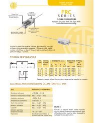
Product specification2Chip Resistor Surface MountRVSERIES0805/1206/2512 (Pb Free)9SCOPEThis specification describes RV0805/1206/2512 high voltage chip resistorswith lead-free terminations made by thick film process.ORDERING INFORMATIONPart number is identified by the series, size, tolerance, packing type,temperature coefficient, taping reel and resistance value.APPLICATIONS• Converter• Printer equipment• Battery charger• Computer• Automotive industry• Power supplyYAGEO ORDERING CODECTC CODERV XXXX X X X XX XXXX L(1) (2) (3) (4) (5) (6) (7)(1) SIZE0805/1206/2512(2) TOLERANCEF = ±1%J = ±5%(3) PACKAGING TYPER = Paper/PE taping reelK = Embossed taping reelORDERING EXAMPLEThe ordering code of a RV1206 chip resistor, value1M X with ±5% tolerance, supplied in 7-inch tapereel is: RV1206JR-071ML.NOTEa. The “L” at the end of the code is only for ordering. On the reellabel, the standard CTC or 12NC will be mentioned anadditional stamp “LFP”= lead free production.b. Products with lead in terminations fulfil the same requirementsas mentioned in this datasheet.c. Products with lead in terminations will be phased out in thecoming months (before July 1st, 2006)(4) TEMPERATURE COEFFICIENT OF RESISTANCE– = Base on spec(5) TAPING REEL07 = 7 inch dia. Reel(6) RESISTANCE VALUE5R6, 56R, 560R, 56K, 27M(7) RESISTOR TERMINATIONS (a)L = Lead-free terminations (matte tin)Feb 14, 2006 V.0www.yageo.com
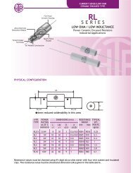
YNSC001YNSC004Chip Resistor Surface MountRVSERIES0805/1206/2512 (Pb Free)Product specification39MARKINGRV0805/1206/2512Fig. 103Value=10 KΩE-24 series: 3 digitsFirst two digits for significant figure and 3rd digit for number of zeros00Fig. 2 Value=10 KΩBoth E-24 and E-96 series: 4 digitsFirst three digits for significant figure and 4th digit for number of zerosFor marking codes, please see EIA-marking code rules in data sheet “Chip resistors marking”.CONSTRUCTIONThe resistors are constructed out of a high-grade ceramicbody. Internal metal electrodes are added at each end andconnected by a high voltage resistive paste. Thecomposition of the paste is adjusted to give theapproximate required resistance and laser cutting of thisresistive layer that achieves tolerance trims the value. Theresistive layer is covered with an overcoat and printedwith the resistance value. Finally, the two externalterminations (matte tin) are added. See fig. 3.OUTLINESFor dimension see Table 1HI 2overcoatresistive layerinner electrodeterminationceramic substrateovercoatDIMENSIONSI 1Table 1 For outlines see fig. 3TYPE L (mm) W (mm) H (mm) I1 (mm) I2 (mm)WRV0805 2.00 ±0.10 1.25 ±0.10 0.50 ±0.10 0.35 ±0.20 0.35 ±0.20RV1206 3.10 ±0.10 1.60 ±0.15 0.55 ±0.10 0.45 ±0.20 0.40 ±0.20RV2512 6.35 ±0.10 3.10 ±0.15 0.55 ±0.10 0.60 ±0.20 0.50 ±0.20LYNSC057Fig. 3Chip resistor outlinesFeb 14, 2006 V.0www.yageo.com
Chip Resistor Surface MountRVSERIES0805/1206/2512 (Pb Free)Product specification49ELECTRICAL CHARACTERISTICSTable 2TYPERESISTANCERANGERatedPowerOperatingTemperatureRangeCHARACTERISTICSMax.WorkingVoltageMax.OverloadVoltageDielectricWithstandingVoltageTemperatureCoefficientof ResistanceRV0805RV12065% (E-24) 100K Ω to 10M Ω1% (E-24/E-96) 100K Ω to 10M Ω5% (E-24) 100K Ω to 27M Ω1% (E-24/E-96) 100K Ω to 10M ΩRV2512 5% (E-24) 4.7M Ω to 16M Ω 1 W1/8 W 400 V 800 V 800 V–55 °C to1/4 W +155 °C 500 V 1,000 V 1,000 V500 V 1,000 V 1,000 V±200 ppm/°CFOOTPRINT AND SOLDERING PROFILESFor recommended footprint and soldering profiles,please see the special data sheet “Chip resistorsmounting”.ENVIRONMENTAL <strong>DATA</strong>For material declaration information (IMDS-data) ofthe products, please see the separated info“Environmental data” conformed to EU RoHS.PACKING STYLE AND PACKAGING QUANTITYTable 3 Packing style and packaging quantityPACKING STYLE REEL DIMENSION RV0805 RV1206 RV2512Paper/PE taping reel (R) 7" (178 mm) 5,000 5,000 ---Embossed taping reel (K) 7" (178 mm) --- --- 4,000NOTE1. For Paper/PE/Embossed tape and reel specification/dimensions, please see the special data sheet “Packing” document.Feb 14, 2006 V.0www.yageo.com
Chip Resistor Surface MountRVSERIES0805/1206/2512 (Pb Free)Product specification59FUNCTIONAL DESCRIPTIONPRODUCT CHARACTERIZATIONStandard values of nominal resistance are taken from the E24 series or E96 series for resistors with a toleranceof 5% or 1%. The values of the E24/E96 series are in accordance with “IEC publication 60063”.OPERATING TEMPERATURE RANGERange: –55°C to +155°CLIMITING VALUESTable 4TYPE LIMITING VOLTAGE (1)(V)LIMITING POWER (2)(W)VR0805 400 1/8VR1206 500 1/4VR2512 500 1POWER RATINGThe power that the resistor can dissipate dependson the operating temperature; see Fig. 4.P max(%P rated )MRA632NOTES1. The maximum voltage that may be continuously applied to theresistor element, see “IEC publication 60115-8” and “IECpublication 60115-2”.2 Each type rated power at 70°C.100500−55 0 5070 100 155T amb (°C)Fig. 4Maximum dissipation (P max ) in percentage of ratedpower as a function of the operating ambienttemperature (T amb )RATED VOLTAGEThe DC or AC (rms) continuous working voltagecorresponding to the rated power is determined bythe following formula:V = √(P X R)WhereV = Continuous rated DC orAC (rms) working voltage (V)P = Rated power (W)R = Resistance value (X)Feb 14, 2006 V.0www.yageo.com
Chip Resistor Surface MountRVSERIES0805/1206/2512 (Pb Free)Product specification69TESTS AND REQUIREMENTSTable 5 Test condition, procedure and requirementsTEST TEST METHOD PROCEDURE REQUIREMENTSTemperatureCoefficient ofResistance(T.C.R.)MIL-STD-202F-method 304;JIS C 5202-4.8At +25/–55 °C and +25/+125 °CFormula:R 2 –RT.C.R= ------------------------- 1×10 6 (ppm/°C)R 1 (t 2 –t 1 )Wheret 1 =+25 °C or specified room temperaturet 2 =–55 °C or +125 °C test temperatureR 1 =resistance at reference temperature in ohmsR 2 =resistance at test temperature in ohmsRefer to table 2Thermal Shock MIL-STD-202F-method 107G;IEC 60115-1 4.19At –65 (+0/–10) °C for 2 minutes and at +155(+10/–0) °C for 2 minutes; 25 cycles±(0.5%+0.05 Ω) for 1% tol.±(1.0%+0.05 Ω) for 5% tol.LowTemperatureOperationMIL-R-55342D-Para 4.7.4At –65 (+0/–5) °C for 1 hour; RCWV appliedfor 45 (+5/–0) minutes±(0.5%+0.05 Ω) for 1% tol .±(1.0%+0.05 Ω) for 5% tol.No visible damageShort TimeOverloadMIL-R-55342D-Para 4.7.5;IEC 60115-1 4.132.5 × RCWV applied for 5 seconds(Votalge ≤ 2 x V max ) at room temperature±(1.0%+0.05 Ω) for 1% tol.±(2.0%+0.05 Ω) for 5% tol.No visible damageInsulationResistanceMIL-STD-202F-method 302;IEC 60115-1 4.6.1.1One DC voltage applied for 1 minuteDetails see below table 6≥10 GΩDielectricWithstandVoltageMIL-STD-202F-method 301;IEC 60115-1 4.6.1.1One DC voltage applied for 1 minuteDetails see below table 6No breakdown or flashoverResistance toSolderingHeatMIL-STD-202F-method 210C;IEC 60115-1 4.18Unmounted chips; 260 ±5 °C for 10 ±1seconds±(0.5%+0.05 Ω) for 1% tol.±(1.0%+0.05 Ω) for 5% tol.No visible damageLife MIL-STD-202F-method 108A;IEC 60115-1 4.25.1At 70±2 °C for 1,000 hours; RCWV applied for1.5 hours on and 0.5 hour off±(1%+0.05 Ω) for 1% tol.±(3%+0.05 Ω) for 5% tol.Feb 14, 2006 V.0www.yageo.com
Chip Resistor Surface MountRVSERIES0805/1206/2512 (Pb Free)Product specification79Table 5 Test condition, procedure and requirements (continued)TEST TEST METHOD PROCEDURE REQUIREMENTSSolderability MIL-STD-202F-method 208A;IEC 60115-1 4.17Solder bath at 245±3 °CDipping time: 2±0.5 secondsWell tinned (≥95% covered)No visible damageBendingStrengthJIS C 5202.6.14;IEC 60115-1 4.15Resistors mounted on a 90 mm glass epoxyresin PCB (FR4)±(1.0%+0.05 Ω) for 1% tol.±(1.0%+0.05 Ω) for 5% tol.Bending: 5 mmNo visible damageResistance toSolventMIL-STD-202F-method 215;IEC 60115-1 4.29lsopropylalcohol (C 3 H 7 OH) or dichloromethane(CH 2 Cl 2 ) followed by brushingNo smearedNoise JIS C 5202 5.9;IEC 60115-1 4.12Maximum voltage (V rms ) applied. Resistors range ValueR < 100 Ω10 dB100 Ω ≤ R < 1 KΩ 20 dB1 KΩ ≤ R < 10 KΩ 30 dB10 KΩ ≤ R < 100 KΩ 40 dB100 KΩ ≤ R < 1 MΩ 46 dB1 MΩ ≤ R ≤ 22 MΩ 48 dBHumidity(steady state)JIS C 5202 7.5;IEC 60115-8 4.24.81,000 hours; 40±2 °C; 93(+2/–3)% RHRCWV applied for 1.5 hours on and 0.5 hour off±(0.5%+0.05 Ω) for 1% tol.±(2.0%+0.05 Ω) for 5% tol.LeachingEIA/IS 4.13B;Solder bath at 260±5 °CNo visible damageIEC 60115-8 4.18Dipping time: 30±1 secondsIntermittentOverloadJIS C 5202 5.8At room temperature; 2.5 × RCWV applied for1 second on and 25 seconds off; total 10,000cycles±(1.0%+0.05 Ω) for 1% tol.±(2.0%+0.05 Ω) for 5% tol.Resistance toVibrationOn requestOn requestMoistureResistanceHeatMIL-STD-202F-method 106F;IEC 60115-1 4.24.242 cycles; total 1,000 hoursShown as Fig. 5±(0.5%+0.05Ω) for 1% tol.±(2.0%+0.05Ω) for 5% tol.No visible damageTable 6 Criteria of rated continued working voltage and overload voltageTYPE RV0805 RV1206 RV2512Voltage (DC/unit: V) 800 1,000 1,000Feb 14, 2006 V.0www.yageo.com
Chip Resistor Surface MountRVSERIES0805/1206/2512 (Pb Free)Product specification89temperature[°C]7550250initial drying24 hoursinitial measurementsas specified in 2.2temperaturetolerance±2 °C (±3.6 °F)unless otherwisespecified90 − 98% RH80 − 98%RHrate of change of temperature is unspecified,however, specimens shall not be subjected toradiant heating from chamber conditioning processescirculation of conditioning air shall be at aminimum cubic rate per minute equivalent to10 times the volume of the chambervoltage applied as specified in 2.480 − 98%90 − 98% RH RH90 − 98% RH+10 °C (+18 °F)−2 °C (−3.6 °F)end of final cycle;measurementsas specified in 2.7optional sub-cycle if specified(2.3); sub-cycle performed duringany 5 of the first 9 cycles; humidityuncontrolled during sub-cycleprior to firstcycle onlySTEP1STEP2STEP3 STEP4 STEP5 STEP6one cycle 24 hours; repeat as specified in 2.5STEP7HBK07305 10 1520time [h]25Fig. 5 Moisture resistance test requirementsFeb 14, 2006 V.0www.yageo.com
Chip Resistor Surface MountRVSERIES0805/1206/2512 (Pb Free)Product specification99REVISION HISTORYREVISION DATE CHANGE NOTIFICATION DESCRIPTIONVersion 0 Feb 14, 2006 - - New datasheet for high voltage chip resistors sizes of 0805/1206/2512, 5%,1% tolerance with lead-free terminationsFeb 14, 2006 V.0www.yageo.com