СкаÑаÑÑ PDF (PDF manual download)
СкаÑаÑÑ PDF (PDF manual download)
СкаÑаÑÑ PDF (PDF manual download)

Create successful ePaper yourself
Turn your PDF publications into a flip-book with our unique Google optimized e-Paper software.
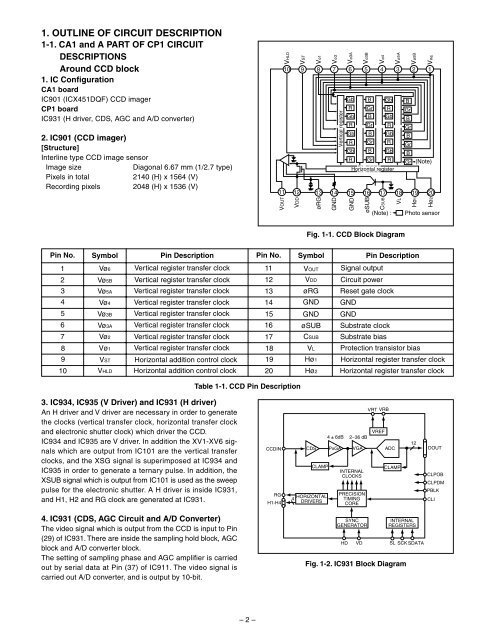
1. OUTLINE OF CIRCUIT DESCRIPTION1-1. CA1 and A PART OF CP1 CIRCUITDESCRIPTIONSAround CCD block1. IC ConfigurationCA1 boardIC901 (ICX451DQF) CCD imagerCP1 boardIC931 (H driver, CDS, AGC and A/D converter)2. IC901 (CCD imager)[Structure]Interline type CCD image sensorImage sizeDiagonal 6.67 mm (1/2.7 type)Pixels in total2140 (H) x 1564 (V)Recording pixels 2048 (H) x 1536 (V)VST911 12 13VOUTVHLD10VDD8 7 6 5 4 3 2 114GNDVertical registerGb B Gb BR Gr R GrGb B GbBR Gr R GrGb B Gb BRGbRGrBGrRGbRGrBGr (Note)Horizontal register15GND16 17CSUB(Note) :18 19 20VLPhoto sensorFig. 1-1. CCD Block DiagramPin No.SymbolPin DescriptionPin No.SymbolPin Description12345678910Vø6Vø5BVø5AVø4Vø3BVø3AVø2Vø1VSTVHLDVertical register transfer clockVertical register transfer clockVertical register transfer clockVertical register transfer clockVertical register transfer clockVertical register transfer clockVertical register transfer clockVertical register transfer clockHorizontal addition control clockHorizontal addition control clock11121314151617181920VOUTVDDøRGGNDGNDøSUBCSUBVLHø1Hø2Signal outputCircuit powerReset gate clockGNDGNDSubstrate clockSubstrate biasProtection transistor biasHorizontal register transfer clockHorizontal register transfer clockTable 1-1. CCD Pin Description3. IC934, IC935 (V Driver) and IC931 (H driver)An H driver and V driver are necessary in order to generatethe clocks (vertical transfer clock, horizontal transfer clockand electronic shutter clock) which driver the CCD.IC934 and IC935 are V driver. In addition the XV1-XV6 signalswhich are output from IC101 are the vertical transferclocks, and the XSG signal is superimposed at IC934 andIC935 in order to generate a ternary pulse. In addition, theXSUB signal which is output from IC101 is used as the sweeppulse for the electronic shutter. A H driver is inside IC931,and H1, H2 and RG clock are generated at IC931.CCDINRGH1-H4CDSCLAMP4HORIZONTALDRIVERS2~36 dBPRECISIONTIMINGCOREVRT VRBVREFPxGA VGA ADCINTERNALCLOCKSCLAMP12DOUTCLPOBCLPDMPBLKCLI4. IC931 (CDS, AGC Circuit and A/D Converter)The video signal which is output from the CCD is input to Pin(29) of IC931. There are inside the sampling hold block, AGCblock and A/D converter block.The setting of sampling phase and AGC amplifier is carriedout by serial data at Pin (37) of IC911. The video signal iscarried out A/D converter, and is output by 10-bit.SYNCGENERATORHDVDINTERNALREGISTERSSL SCK SDATAFig. 1-2. IC931 Block Diagram– 2 –