СкаÑаÑÑ PDF (PDF manual download)
СкаÑаÑÑ PDF (PDF manual download)
СкаÑаÑÑ PDF (PDF manual download)

You also want an ePaper? Increase the reach of your titles
YUMPU automatically turns print PDFs into web optimized ePapers that Google loves.
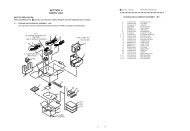
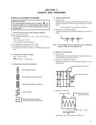
1-4. ST1 STROBE CIRCUIT DESCRIPTION1. Charging CircuitWhen UNREG power is supplied to the charge circuit and theCHG signal from microprocessor becomes High (3.3 V), thecharging circuit starts operating and the main electorolyticcapacitor is charged with high-voltage direct current.However, when the CHG signal is Low (0 V), the chargingcircuit does not operate.1-1. Power switchWhen the CHG signal switches to Hi, Q5407 turns ON andthe charging circuit starts operating.1-2. Power supply filterC5401 constitutes the power supply filter. They smooth outripples in the current which accompany the switching of theoscillation transformer.1-3. Oscillation circuitThis circuit generates an AC voltage (pulse) in order to increasethe UNREG power supply voltage when drops in currentoccur. This circuit generates a drive pulse with a frequencyof approximately 50-100 kHz. Because self-excited light omissionis used, the oscillation frequency changes according tothe drive conditions.2. Light Emission CircuitWhen RDY and TRIG signals are input from the ASIC expansionport, the stroboscope emits light.2-1. Emission control circuitWhen the RDY signal is input to the emission control circuit,Q5409 switches on and preparation is made to let currentflow to the light emitting element. Moreover, when a STOPsignal is input, the stroboscope stops emitting light.2-2. Trigger circuitWhen a TRIG signal is input to the trigger circuit, D5405switches on, a high-voltage pulse of several kilovolts is generatedinside the trigger circuit, and this pulse is then appliedto the light emitting part.2-3. Light emitting elementWhen the high-voltage pulse form the trigger circuit is appliedto the light emitting part, currnet flows to the light emittingelement and light is emitted.Beware of electric shocks.1-4. Oscillation transformerThe low-voltage alternating current which is generated by theoscillation control circuit is converted to a high-voltage alternatingcurrent by the oscillation transformer.1-5. Rectifier circuitThe high-voltage alternating current which is generated atthe secondary side of T5401 is rectified to produce a highvoltagedirect current and is accumulated at electrolytic capacitorC5512.1-6. Voltage monitoring circuitThis circuit is used to maintain the voltage accumulated atC5512 at a constance level.After the charging voltage is divided and converted to a lowervoltage by R5417, R5419 and R5420, it is output to the microprocessoras the monitoring voltage VMONIT. When thisVMONIT voltage reaches a specified level at the microprocessor,the CHG signal is switched to Low and charging isinterrupted.– 5 –