Samsung SCH-210 service manual.pdf - Free
Samsung SCH-210 service manual.pdf - Free
Samsung SCH-210 service manual.pdf - Free

Create successful ePaper yourself
Turn your PDF publications into a flip-book with our unique Google optimized e-Paper software.
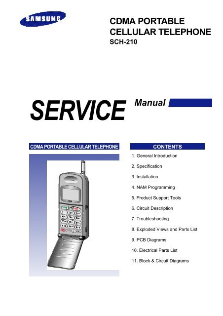
CDMA PORTA B L EC E L L U L A RT E L E P H O N E<strong>SCH</strong>-<strong>210</strong>S E RVICE ManualCDMA PORTABLE CELLULAR TELEPHONECONTENTS1. General Introduction2. Specification3. Installation4. NAM Programming5. Product Support Tools6. Circuit Description7. Troubleshooting8. Exploded Views and Parts List9. PCB Diagrams10. Electrical Parts List11. Block & Circuit Diagrams
<strong>Samsung</strong> Electronics Co.,Ltd.GH68-60756A
1. General IntroductionThe <strong>SCH</strong>-<strong>210</strong> cellular phone functions as both analog cellular phone working in AMPS (Advanced MobilePhone Service) mode and digital cellular phone working in CDMA (Code Division Multiple Access) mode.CDMA type digital mode applies DSSS (Direct Sequential Spread spectrum) mode which first came to beused in the military.The DSSS reduces channel cross talk and allow to use one frequency channel by multiple users in the samespecific area, resulting in increase of channel capacity to about ten times compared to that of analog modecurrently used.Soft/Softer Handoff, Hard Handoff, and Dynamic RF Power Control technologies are combined into thisphone to reduce the call drop while usage.CDMA digital cellular network consists of MSO (Mobile Switching Office), BSC (Base Station Controller),BTS (Base Station Transmission System), and MS (Mobile Station). MS meets the specifications of the below:IS-95A : Mobile Station-Base Station Compatibility Standard for Dual-Mode Wideband Spread SpectrumCellular SystemIS-96A : Speech Service Option 1 Standard for Dual-Mode Wideband Spread Spectrum Cellular SystemsIS-98A : Standards for Dual-Mode Wideband Spread Spectrum Cellular Mobile StationIS-126 : Mobile Station Loopback Service Options Standard<strong>SCH</strong>-<strong>210</strong> is composed of main handset, rapid charger, cradle, two batteries (1300 mAh, 850 mAh), handsfreekit, and travel charger. Hands-<strong>Free</strong> Kit is designed to be operated in half-duplex mode taking turnarounddelay between the phone and the system into account.<strong>Samsung</strong> Electronics - Contents may change without notice. 1-1
2. Specification2-1 GeneralFrequency Range Digital Mode Analog ModeTransmitter : 824.64 ~ 848.37 MHz 824.04 ~ 848.97 MHzReceiver : 869.64 ~ 893.37 MHz 869.04 ~ 893.97 MHzChannel Spacing : 1.23 MHz 30 kHzNumber of Channels : 20 FA 832 CHsDuplex Spacing: 45 MHzFrequency Stability : 2.5 ppm ( 30 ~ £ 60 -22 ~ 140 )Operating Temperature : 20 ~ £ 50 ( 4 ~ 122 )Operating VoltageHHP : 7.2V DC ( 10 )Hands-free : 13.7V DC ( 10 )Size and Weightincluding standard battery : 130 51 27.5 mm, 205 g (5.12 2 0.94 inch, 7.2 oz)including extended-life battery : 130 51 37 mm, 207 g (5.12 2 1.46 inch, 7.4 oz)Operating TimeDigital mode Standby Time : about 50 ~ 55 hours (with standard battery): about 85 ~ 90 hours (with extended-life battery)Talk Time : about 150 min (with standard battery): about 250 min (with extended-life battery)Analog Standby Time : about 10 ~ 12 hours (with standard battery): about 16 ~ 18 hours (with extended-life battery)Talk Time : about 100 min (with standard battery): about 170 min (with extended-life battery)2-2 Analog ModeTRANSMITTERRF output power : 0.6 W ( 2/ 4 dB)Carrier ON/OFF Conditions"ON" Condition : within 3 dB of specification output (in 2mS)"OFF" Condition : below 60 dBm (in 2mS)CompressorCompression Rate : 2:1Attack Time: 3 mSRecovery Time: 13.5 mSReference Input : Input level for producing a nominal 2.9 kHz peak frequencydeviation of transmitted carrier<strong>Samsung</strong> Electronics - Contents may change without notice. 2-1
SpecificationPreamphasis: 6 dB/OCT within 0.3 ~ 3 kHzMaximum Frequency DeviationF3 of G3 : 12 kHz ( 10 )Supervisory Audio Tone : 2 kHz ( 10 )Signaling Tone : 8 kHz ( 10 )Wideband Data : 8 kHz ( 10 )Post Deviation Limiter Filter3.0 kHz ~ 5.9 kHz : above 40LOG (F/3000) dB5.9 kHz ~ 6.1 kHz : above 35 dB6.1 kHz ~ 15 kHz : above 40LOG (F/3000) dBOver 15 kHz: above 28 dBSpectrum Noise SuppressionFor All Modulationf 20 kHz ~ f 45 kHz : above 26 dBFor Modulation by Voice and SATf 45 kHz : above 63 10LOG (Py) dBFor Modulation by WBD (without SAT) and ST (with SAT)f 45 kHz ~ f 60 kHz : above 45 dBf 60 kHz ~ f 90 kHz : above 65 dBf 90 kHz ~ 2f : above 63 10LOG (Py) dB(where f = carrier frequencyPy= mean output power in watts)Harmonic and Conducted Spurious Emissions : above 43 10LOG (Py) dBRECEIVERDE-Emphasis : 6 dB/OCT within 0.3 ~ 3 kHzExpanderExpansion Rate : 1:2Attack Time: within 3 mSRecovery Time: within 13.5 mSReference Input : Output level to a 1000 Hz tone from a carrier within 2 . 9kHz peak frequency deviationSensitivity : 12 dB SINAD/ 116 dBmIntermodulation Spurious Response AttenuationRSSI Range: above 65 dB: above 60 dBProtection Against Spurious Response Interference : above 60 dBIn Band Conducted Spurious EmissionsTransmit Band : below 60 dBmReceive Band : below 80 dBmOut of Band Conducted Spurious Emissions : below 47 dBm2-2 <strong>Samsung</strong> Electronics - Contents may change without notice.
SpecificationRadiated Spurious EmissionsFrequency Range25 ~ 70 MHz70 ~ 130 MHz130 ~ 174 MHz174 ~ 260 MHz260 ~ 470 MHz470 ~ 1 GHzMaximum Allowable EIRP45 dBm41 dBm41 ~ 32 dBm32 dBm32 ~ 26 dBm21 dBm2-3 Digital ModeWaveform Quality : above 0.944Time Reference : within 1uSRX Sensitivity : 104 dBm, FER = within 0.5%Dynamic Range : 104 dBm ~ 25 dBm, FER = within 0.5%TX Output Power: Maximum 320 mW (25dBm)TX Frequency Deviation : within 300 HzOccupied Band Width: 1.32 MHzTX Conducted Spurious Emissions : 900 kHz below 42 dBc / 30 kHz: 1.98 MHz below 54 dBc / 30 kHzMinimum TX Power Control : below 50 dBmOpen Loop Power Control : 25 dBm 57.0 dBm ~ 38.5 dBm65 dBm 17.5 dBm ~ £ 1.5 dBm104 dBm £ 18.0 dBm ~ £ 30.0 dBmStandby Output Power : below 61 dBmClosed Loop TX Power Control Range : Test 1 beyond 24 dBTest 2 0 mS ~ 2.5 mSTest 3 beyond 24 dBTest 4 beyond 24 dBTest 5 beyond 24 dB<strong>Samsung</strong> Electronics - Contents may change without notice. 2-3
SpecificationMSC Transmitter FrequencyFA NO. CH. NO. CENTER FREQUENCY FA NO. CH. NO. CENTER FREQUENCY1 1011 824.640MHz 11 404 837.120MHz2 29 825.870MHz 12 445 838.350MHz3 70 827.100MHz 13 486 839.580MHz4 111 828.330MHz 14 527 840.810MHz5 152 829.560MHz 15 568 842.040MHz6 193 830.790MHz 16 609 843.270MHz7 234 832.020MHz 17 650 844.270MHz8 275 833.250MHz 18 697 845.910MHz9 316 834.480MHz 19 738 847.140MHz10 363 835.890MHz 20 779 848.370MHzMSC Receiver FrequencyFA NO. CH. NO. CENTER FREQUENCY FA NO. CH. NO. CENTER FREQUENCY1 1011 869.640MHz 11 404 882.120MHz2 29 870.870MHz 12 445 883.350MHz3 70 872.100MHz 13 486 884.580MHz4 111 873.330MHz 14 527 885.810MHz5 152 874.560MHz 15 568 887.040MHz6 193 875.790MHz 16 609 888.270MHz7 234 877.020MHz 17 650 889.270MHz8 275 878.250MHz 18 697 890.910MHz9 316 879.480MHz 19 738 892.140MHz10 363 880.890MHz 20 779 893.370MHz2-4 <strong>Samsung</strong> Electronics - Contents may change without notice.
Specification2-4 CDMA Debug Display Information (menu 8)IN IDLE MODESxxxxx : SID (System ldentification) toggleNxxxxx : NID (Network Identification) toggleSIDxxxxx Slx xT xx Rxxx xxPxxx CHxxxxIN CONVERSATION MODESlx : Slot cycle index (lowest between the systemand the phone will be used)Handset Status : 0 - Acquisition1 - Synchronization2 - Paging (Idle)3 - Traffic Initialization4 - Traffic Mode5 - ExitT-xx : Tx adjust, Value ranges from +63 ~-63dBDxxx or Rxxx : sector power in dBm-xx : ec/IoTVx RVx xx xT xx Rxxx xxPxxx CHxxxxPxxx : PN offset or Pilot #CHxxxx : channel numberTV : Tx vocoder rate (8 is full rate, 1 is 1/8th rate)RV : Rx vocoder rate (8 is full rate, 1 is 1/8th rate)xx : Walsh code used in traffic channel2-5 FM Debug Display Information (menu 8)SIDxxxxx : FM Home System IDPWRx : Power Level 0~7SATx : Supervisory Audio Tone code (0~3)SIDxxxxxPWRxSATxxRSSIxxxCHxxxxx (Using Frequency Band) : A Band or B BandRSSIxxx : RSSI valueCHxxx : Using Channel<strong>Samsung</strong> Electronics - Contents may change without notice. 2-5
Specification2-6 <strong>Samsung</strong> Electronics - Contents may change without notice.
3. Installation3-1 Installing a Battery Pack1. To attach the battery pack after charging, alignit with the phone about 1cm (1/2") away fromits place so that the two arrows on the phoneare seen, the battery charge contacts pointingdownward.3. To remove the battery pack, release it bypressing the button on the rear of the phone.4. Slide the battery pack downward about 1cm(1/2") and lift it away from the phone.2. Slide the battery pack upwards until it clicksfirmly into position. The phone is now readyto be turned on.Press this button to releasethe battery pack3-2 For Desk Top Use1. Choose a proper location to install the chargerfor desk top use.2. Plug the power cord of the charger into anappropriate wall socket. When the power isconnected correctly, the lamps turn on briefly.3. To charge the battery pack, insert the batterypack into the rear slot of the charger. The lampmarked BAT on the front panel of the chargerlights up red.4. If you do not wish to use the phone whilecharging the battery, insert the phone with thebattery pack attached into the front slot of thecharger. The lamp marked PHONE on thefront panel of the charger lights up red.Figure 3-1 Charging the Phone and Battery<strong>Samsung</strong> Electronics - Contents may change without notice. 3-1
InstallationItem Model Name Service Part#Desk Top Rapid Charger DTC58 GH44-40034AStandard Battery Pack BTL850SB GH43-10104AExtended Battery Pack BTL1350EB GH43-10103ASPECIFICATIONS USING “DTC 58”Product Charging time Stand by time (hours) Talking time (min)(hours) Digital Analog Digital AnalogStandard Battery Pack (Li-ion: 800mAh) 2 ~ 3 50 ~ 55 10 ~ 12 150 100Extendard Battery Pack (Li-ion: 1350mAh) 2.5 ~ 3.5 85 ~ 90 16 ~ 18 250 1703-3 For Mobile Mount3-3-1 Antenna1. Choose a proper location to install theantenna.The center of the roof top provides the bestperformance.The edge of the rear trunk also provides agood performance. However, the antennashould be higher than the roof of the car.In case of on-glass antenna, you shouldalign the antenna base with the round plateto connect the cables correctly.2. Mount the antenna vertically, connect theantenna cable.3. Tighten the antenna nut fully.3-2 <strong>Samsung</strong> Electronics - Contents may change without notice.
Installation3-3-2 Cradle1. Choose a location where it is easy to reach anddoes not interfere with the driver's safeoperation of the car.2. Separate the two halves of the clamshell byremoving the two large slotted screws. See thefigure 3-2.4. Place the cradle onto the remaining half of theclamshell and assemble them by using thescrews.5. Reassemble the two halves of the clamshelltogether. Adjust the mounting angle andtighten the two slotted screws.3. Drill holes and mount the lower half of theclamshell by using the screws.Figure 3-2 Cradle Installation<strong>Samsung</strong> Electronics - Contents may change without notice. 3-3
Installation3-3-3 Hands-<strong>Free</strong> Box1. Drill holes in a proper location for the handsfreebox, attach the mounting bracket by usingthe screws. See the figure 3-3.2. Install the hands-free box into the bracket.3-3-4 Hands-<strong>Free</strong> Microphone1. It is recommended to install the microphonewhere it is 30-45 cm (12-18") away from thedriver. Choose the location where is leastsusceptible to interference caused by externalnoise sources, ie, adjacent windows, radiospeakers, etc. Normal place is the sun visor.2. Once the microphone has been correctlypositioned, connect the microphone wire tothe MIC jack on the hands-free box.Figure 3-3 Hands-<strong>Free</strong> Box Installation3-4 <strong>Samsung</strong> Electronics - Contents may change without notice.
Installation3-3-5 Cables1. Connect the cradle and the hands-free boxwith the data cable. See the figure 3-4.2. Connect the antenna cable to the RF jack of thecradle.3. Connect the power cable as follows:Connect the red wire to the battery (+)terminal, black wire to the battery (-) terminal.Then connect the orange wire to the switchedside of the ignition switch, and then connectthe brown wire to the stereo mute wire fromyour vehicle stereo.Notes:It is recommended to connect the power cabledirectly to the battery to avoid power noise.Make sure the connection, in the vehicle,between the battery (-) terminal and vehiclechassis is made correctly.Make sure the fuse having a proper capacity isused on the power cable.Make sure the cables do not pass over any sharpmetal edge that may damage it.4. Connect the other end of the power cable tothe PWR jack of the hands-free box.Figure 3-4 Cable Connections<strong>Samsung</strong> Electronics - Contents may change without notice. 3-5
Installation3-6 <strong>Samsung</strong> Electronics - Contents may change without notice.
4. NAM Programming4-1 General SetupLCD Display Key in Function47 869#08#9 -selects NAM programmingNAM Program1:General2:Setup NAM11 -choose 'GENERAL.'ESNB0000000VolumeElectronic Serial Number of the phone.CAI version3VolumeThe version of the Common Air Interface supported by the mobile.VOC 13K/8KSO_VOICE_13KOKorVocoder data rate.SCM01101010Volume Station Class Mark displays the power class (bit 0~1),transmission (bit2), slotted (bit5), dual mode (bit6).Lock Code00004-digit codeOKFour-digit number supplied by the user which enableselectronic locking of the phone.Slot ModeYesOKorEnables slot mode.Slot Index2Slot mode index.0 - 7 Specifies the duration and frequency of times that the mobileOKchecks the paging channel. The higher the value, the less often themobile looks at the paging channel, and the more power is saved.Pref NAM(1~4)...Digital prefOKorPreferred system selection for NAM(1~4).Up to four NAMs are allowed for the phone. This lists one of thefour NAMs and allows you to program both the FM and CDMAsettings.<strong>Samsung</strong> Electronics - Contents may change without notice. 4-1
NAM Programming4-2 Setting Up NAM1LCD Display Key in FunctionNAM Program1:General2:Setup NAM1Setup NAM11:Phone #2:FM3:CDMA2 -choose 'Setup NAM1.'1 -choose 'Phone #'.Phone #1234567890Mobile ID #1234567890phone numberOKmobile ID numberOKPhone number.Mobile ID number.Setup NAM11:Phone #2:FM3:CDMA2 -choose 'FM.'FM Home SID20ID numberOKFM Home System ID.The Identification of the cellular system in which the mobilestation subscribes for <strong>service</strong>.Cellular Service provider.FM 1st Chn3341st Paging Channel.channel number Suggested setting is 333 for the A carrier, 334 for the B carrier:OK ranges from 313 to 333 for A and 334 to 354 for B.Primary analog paging channel: setting depends on whetherthe <strong>service</strong> is provided by the A carrier or the B carrier.FM Acq SID (1~6)20ID numberOKFM Acquisition System ID.Enables you to set the phone to acquire up to six SIDs in theanalog mode. If you enter ‘0’ for any SID, the programassumes that you have no more numbers to store.Default setting is 0: ranges from 0 to 32,767: up to six SIDs.FM LockSID (1~6)0ID numberOKFM Lock System ID.Enables you to specify up to six SIDs that the phone is prohibitedfrom acquiring in analog mode. If you enter ‘0’ for any SID, theprogram assumes that you have no more numbers to store. Theuser may be denied <strong>service</strong> when operating within the <strong>service</strong>areas of these systems.Default setting is 0: ranges from 0 to 32,767: up to six SIDs.4-2 <strong>Samsung</strong> Electronics - Contents may change without notice.
NAM ProgrammingLCD Display Key in FunctionAuto RegYesOKorEnables autonomous registration.FM pref...B prefOKorPreferred system selection.FM ACCOLC0OKorFM Access Overload Class.This two-digit number specifies the level of priority assignedto the mobile for accessing the system.Ranges from 0 to 15.Setup NAM11:Phone #2:FM3:CDMA3 -choose 'CDMA.'IMSI MCC000numberOKInternational Mobile Station Identity Mobile Country Code.IMSI MNC00numberOKInternational Mobile Station Identity Mobile Network Code.CDMA pref...B prefOKorPreferred system selection.CDMA ACCOLC0class numberOKCDMA Access Overload Class.This two-digit number specifies the level of priority assignedto the mobile for accessing the system.Ranges from 0 to 15.Pchn Sys A283channel numberOKPrimary CDMA channel for the A carrier.Ranges from 0 to 1,023. 0 indicates no channel.Pchn Sys B384channel numberOKPrimary CDMA channel for the B carrier.Ranges from 0 to 1,023. 0 indicates no channel.Schn Sys A691channel number Secondary CDMA channel for the A carrier.OK Suggested setting is 0: ranges from 0 to 1,023.Schn Sys B777channel number Secondary CDMA channel for the B carrier.OK Suggested setting is 0: ranges from 0 to 1,023.<strong>Samsung</strong> Electronics - Contents may change without notice. 4-3
NAM ProgrammingLCD Display Key in FunctionCD Acq SID(1-6)20ID numberOKCDMA Acquisition System ID.Enables you to set the phone to acquire up to six SIDs in theCDMA mode. If you enter ‘0’ for any SID, the programassumes that you have no more numbers to store.Default setting is 0: ranges from 0 to 32,767: up to six SIDs.CD(1-6)lockSID0ID numberOKCDMA Lock System ID.Enable you to specify up to six SIDs that the phone will beprohibited from acquiring in CDMA mode. If all six SIDs areset to zero, no lock restrictions will be in effect and the phonecan acquire all SIDs.Default setting is 0: ranges from 0 to 32,767 up to six SIDs.CDMA HomeSIDYesOKorCDMA Home System ID.Enables the phone to allow mobile terminated calls while inthe home system. Controls the types of registration allowed forthe phone.CDMAfSIDYesOKorCDMA foreign SID, current status is displayed.changes the status.stores it.CDMAfNIDYesOKorCDMA foreign NID, current status is displayed.changes the system.stores it.SID #120numberOKfirst SID written in the list, current status is displayed.to change, enter new one.stores it.NID #165535numberOKfirst NID written in the list, current status is displayed.to change, enter new one.stores it.4-4 <strong>Samsung</strong> Electronics - Contents may change without notice.
NAM Programming4-3 Quick NAM ProgrammingLCD Display Key in FunctionMenu, 4, 0Select Quick NAM ProgrammingEnter Lock626 Enter Lock Code.NAM Program1:Setup NAM12:Setup NAM21 Choose “NAM1”Phone #1234567890Phone NumberOKPhone Number.Mobile ID #1234567890Mobile ID NumberOKMobile ID Number.SID20NumberOKSystem ID Number.<strong>Samsung</strong> Electronics - Contents may change without notice. 4-5
NAM Programming4-6 <strong>Samsung</strong> Electronics - Contents may change without notice.
5. Product Support Tools5-1 GeneralThese tools enable you to edit or transfer all the EEPROM data of <strong>SCH</strong>-<strong>210</strong> Cellular Phone. For examples,there are three tools; PST (including 'Phone Book Transfer', 'Download', and 'Edit common UI parameters'),Data Transfer.Equipment RequiredPST program, Data transfer program.IBM compatible PC ( above 386, 33MHz, 8MBRAM, DOS 5.0, 500K of memory free to executeprogram, and 1MB of disk space free forsoftware upgrade.)<strong>SCH</strong>-<strong>210</strong> Test Jig7.2V Power SupplyConnectionSoftware Installation1. Insert the PST floppy disk into drive (A:).2. Create an appropriate directory to the drive(C:) for PST software.3. Copy all files of the drive (A:) to the directoryyou made.4. Execute PSTxx.EXE to run the PST program.Note: There are three executable files in the newdirectory you made:PSTxx.EXE : PST program where xx is the PSTversion number.DTRANxx.EXE : Data transfer program.Connect the test jig to COM1 serial port on the PCand connect the interface cable of the test jig to thephone.Caution: When you use the PST program with anotebook PC, you might encounter someproblems. Check your serial port setup in yournotebook PC (see your notebook PC <strong>manual</strong>).Don't worry about the serial port setup when youuse a desktop PC.<strong>Samsung</strong> Electronics - Contents may change without notice. 5-1
Product Support Tools5-2 Product Support Tool (PST)The Product Support Tool(PST) offers you theability to interface with the <strong>SCH</strong>-<strong>210</strong> cellularphone using a personal computer. You canprogram the phone, swap phone data, anddownload software upgrades.Notes:This software is made to be executed on the MS-DOS, not on the DOS mode within Windows95.If this software is executed in Windows bymistake, it may work abnormally and damagethe phone especially while downloading.Please check the mode you are using.You can transfer EEPROM data one unit at atime.It is illegal to copy to several units.EDITING FIELDSOnce you are in a particular screen, you may wantto change a value of any field. A highlightedcursor can be moved to each editable field byusing the arrow keys. A field can only be edited ifthe cursor is on that field (that is, if the field ishighlighted.)1. Begin the editing process by pressing key.2. To accept the new value, press key. Toabort edit mode and return to the old value,press key.3. The value of some field that is fixed types willbe changed by just pressing key.See table 5-1 for the list of editing keys.5-2-1 Getting StartedMAIN MENU SCREEN1. At the DOS prompt, type "PSTxx" where xx isthe release version.2. The Main Menu screen is displayed.Notes:The Main Menu screen shows the basic tasksthat are available.Move the cursor through the menu choices andpress key to select a task.EXITING THE PROGRAM1. Press key until you find the Main Menuscreen.2. Select the "QUIT" option on the Main Menu orpress key, and the PST program isover.5-2-2 Operation ProcedureSERVICE PROGRAMMINGThe Service Programming screens enable you toset and change the <strong>service</strong> parameters of thephones, read and write to internal phone book,and transfer phone book data to other phone.There are six options listed on the ServiceProgramming Main Menu.The parameter modification is done on the "EditParameters NAM" and "Edit Parameters UI"screens. The variables found on those screens canbe preset from a phone or a previously saved file.Select "Read Data from File" or "Read Data fromPhone" to preset the values.READ DATA FROM FILEUse this command to enter the name of a filewhose extension is "mmc". The values read fromthe named file will initialize the parameter valuesseen on the "Edit Parameters NAM" and "EditParameters UI" screens.5-2 <strong>Samsung</strong> Electronics - Contents may change without notice.
Product Support ToolsREAD DATA FROM PHONEUse this command to replace the currentprogrammable parameter values with the valuesthat are currently programmed into the phone.The values are read from the phone that must beproperly connected to the PST with power on.EDIT PARAMETERS NAMUse this command to edit Number AssignmentModule(NAM) items.Function KeysF1 Displays help message about a selectedfieldF6 Takes you to the General settings screenF7~10 Takes you to the NAM(1~4) parametersscreenEsc Takes you back to the Menu screen aftersaving.There are two types of screens :1. General settings : some writable, some readonly2. Parameters associated with NumberAssignment Module 1~4 (NAM1~4)EDIT PARAMETERS UIUse this command to edit User Preference (UI)items.There are two types of UI items :1. Common UI items: Edits User Preference items.Function KeysF1 Displays help message about a selectedfieldF6 Takes you to the next (or previous) UIParameters screenEsc Takes you back to the Menu screen aftersaving.ScreensFirst Screen: Setting 'Auto Setup', 'Alert Select','Volume', 'System', and 'Restrict'Second Screen: Setting 'Time', 'Setup', 'OutgoingCall Log', and 'Incoming CallLog'2. Phone Book: Edits Phone Book's DataFunction KeysF4 Searches by the NameF5 Searches by the NumberF6 Displays the next Name/NumberF9 Clears all memoryEsc Takes you back to the Menu screen aftersaving.Valid vs. Invalid DataUpon startup, all items are initialized "invalid". Allfields display the question marks instead of data.After reading from a phone or a file, if the questionmarks still show in a field, then that item has neverbeen written to the phone or saved to the file.SAVE DATA TO FILEUse this command to save the current parametersin a file. Once you enter a filename, press key to write all current parameters to the file.WRITE ALL TO PHONEUse this command to write the changed parametervalues to the phone.Writing the changed values to the phone may takeup to a minute.Notes:Some items have dependencies on other items,and they will be written to the phone together.If you intend to use this "Write All to Phone"feature, it is recommended that you do a "ReadData from Phone" first, and then make thechanges, so that nothing gets inadvertentlyoverwritten.<strong>Samsung</strong> Electronics - Contents may change without notice. 5-3
Product Support ToolsSOFTWARE DOWNLOADERUse this screen to download new software to thephone. The various windows are displayed toinform the user of the phone data and the progressof download.The software downloader task of the PST isresponsible for downloading a BIN file into theflash memory on the phone. It verifies that thegiven BIN file is compatible with the target phone,and performs all the protocol necessary tosuccessfully download the file.To begin a software downloader, use the followingprocedure.1. Press key to choose a BIN file of the newsoftware to be loaded into the phone. An Editbox will pop up asking for BIN file name. Enterfull file name or press key to see thelists of BIN files in the current directory. Usingthe arrow key, choose the appropriate BIN file,then press key.SETUPYou can setup <strong>SCH</strong>-<strong>210</strong> only. Use this screen tochoose the phone type you want to setup.Function keysSPACE : Scrolls through menu.ENTER : Accepts the phone type chosen.ESC and ALT-x : Cancels operation and returns toMain Menu.QUITYou can exit the PST program.2. Press key to change the mode of thephone from hands-free mode to DM offlinemode. This function is to view the software andhardware version of the phone. By setting thephone to DM offline mode, the upper leftwindow should display the phone's data. If thephone fails to change mode, an error soundand message will occur. In that case, pleasecheck the power, link, and COM portconfiguration.3. Press key to begin download.Various messages and progress bar will informthe user of the progress of the download.Caution: DO NOT REMOVE POWER WHILETHE PHONE IS BEING DOWNLOADED !USE A FULLY CHARGED BATTERY TOOPERATE HANDSET.4. Press key to return to Main Menu.5-4 <strong>Samsung</strong> Electronics - Contents may change without notice.
Product Support Tools5-3 Data Transfer programWhen the main board of a customer's cellularphone is required to be replaced with a new one,or the customer is needed to use a phone lent fromthe <strong>service</strong> center while his phone is <strong>service</strong>d, thisfeature is used to transfer(copy) all the EEPROMdata of the customer's phone into the new board orthe lent phone to keep the information thecustomer had stored into his phone personally.5-3-1 Getting Started1. Run the DTRANxx.EXE file. If you run the filefor the first time, the message 'INITIAL FILE ISCREATED' appears. Do not delete the createdfile because the file creates DTRANxx.CFG tostore environment setup data. The messagedoes not appear once you have run theprogram.2. Press any key to go to next procedure.Function KeysFl Reads EEPROM data from thecustomer's cellular phone.3. Press key to read EEPROM data from thecustomer's cellular phone. On screen, 'Changethe mode of the phone from HANDS-FREEmode to DM mode' message appears. On theLCD display of the phone, 'AUTO TEST' and'WRITE EEPROM' messages appear. If thephone is already in DM(Diagnostic Monitor)mode, the message does not appear.4. After the mode is changed to DM, EEPROMdata on the cellular phone is read by PC. Youcan monitor the reading procedure on thescreen.5. When the data reading is completed, 'Replacethe source phone with the target phone andpress when ready' message appears onthe screen.6. Press any key to clear the message. The cellularphone displays 'DELETED' and '300-300-3000'instead of greeting and phone numberrespectively. All the features of the phoneincluding ESN are reset to default status, andthe phone can not be operated.F5Writes the data of the customer's phoneinto the EEPROM on the new board.7. Remove the phone from the test jig and connectthe new phone to the test jig.ALT+X Exits programming and returns to DOSmode.5-3-2 Operation Procedure1. On standby mode, 'Please check thecommunication link between your PC and thephone prior to beginning ...' messages appearon the screen. You are ready to transfer data.2. Switch the phone power on after you have runthe program.Caution: If you try to perform reading againwithout writing after reading is already done once,the error message 'READING FROM THE PHONEWAS ALREADY BEEN CARRIED OUT,WRITING SHOULD BE CARRIED OUT' appearson the screen.8. Press key to perform writing EEPROMdata. You can monitor the writing procedureon the screen.9. When the data writing is completed, the phonewill reset. The program returns to standbymode and is ready to read data from anotherphone. 'WELL DONE, DATA TRANSFER ISCOMPLETED' appears on the screen.10. Check if the transferred EEPROM data is thesame.<strong>Samsung</strong> Electronics - Contents may change without notice. 5-5
Product Support ToolsTable 5-1. Editing keys.KeyArrow KeysEnterEscDeleteBack SpaceHomeDescriptionMove the field cursor to the next editable field in the direction of the arrow. If in editmode, the left and right arrows move the cursor left and right within that field.Enters edit mode. Some fields have a limited number of valid values, and pressing key repeatedly cycles through the options. After editing, and press the key again. Then exits edit mode, accepting a new value.Aborts edit mode.Deletes the selected charater in Edit mode.Backs towards the beginning of the line and deletes.Moves the edit cursor to the beginning of the string.5-6 <strong>Samsung</strong> Electronics - Contents may change without notice.
6. Circuit Description6-1 Logic Section6-1-1 Power SupplyWith the battery installed on the phone and bypressing the PWR key, the VBATT and ON_SWsignals will be connected. This will turn on Q102(2SC4081BR) and will drive DC-DC converter(U123) to output 5.0V. This in turn will besupplied to pin 6 of regulators (U121 and U122),thus releasing them from the shut-down state tooutput regulated 3.3V.The VBATT applied to ON_SW will turn on Q103(DTC144EE) resulting in the signalON_SW_SENSE to change state from HIGH toLOW. This will allow MSM to send out PS_HOLD(logical HIGH) to turn on Q102 even after thePWR key is released.The voltage (+3.3V) from U121 is used in thedigital parts of MSM and BBA. The voltage(+3.3AV) from U122 is used in the analog part ofBBA. The voltage from U124 (output of 5V) is usedfor the audio circuitry.CPUINTEL 80186 CMOS type 16-bit microprocessor isused for the main processing. The CPU controls allthe circuitry. For the CPU clock, 27MHz resonatoris used.FLASH ROMOne 8 MBIT FROM is used to store the terminal'sprogram. Using the down-loading program, theprogram can be changed even after the terminal isfully assembled.SRAMOne 2 MBIT SRAM is used to store the internalflag information, call processing data, and timerdata.6-1-2 Logic PartThe Logic part consists of internal CPU of MSM,RAM, ROM and EEPROM. The MSM receivesTCXO and CHIPX8 clock signals from the BBAand controls the phone during the CDMA and theFM mode. The major components are as follows:CPU : INTEL 80186 coreFROM : U126 (MBM29LV800T) - 8MBITSRAMFLASH ROM: U127 (KM68V2000I) - 2MBITSTATIC RAMEEPROM : U113 (AT24C128) - 128KBIT SERIALEEPROMEEPROMOne 128 KBIT EEPROM is used to store ESN,NAM, power level, volume level, and telephonenumber.KEYPADFor key recognition, key matrix is setup usingSCAN0-6 of STORE signals and KEY0-3 of inputports of MSM. Eight LEDs and backlight circuitryare included in the keypad for easy operation inthe dark.LCD MODULELCD module contains a controller which willdisplay the information onto the LCD by 8-bit datafrom the MSM. It also consists a DC-DC converterto supply -3.5V for fine view angle and LCDreflector to improve the display efficiency.<strong>Samsung</strong> Electronics - Contents may change without notice. 6-1
Circuit Description6-1-3 Baseband PartMOBILE SYSTEM MODEM (MSM)The MSM equipped with the INTEL 80186 CPUcore is an important component of the CDMAcellular phone. The MSM comes in a 176 pinsTQFP package. The interface block diagram isshown on page 6-3.ADC InterfaceADC_CLK (pin 3), ADC_ENABLE (pin 1) andADC_DATA (pin 2) are required to control theinternal ADC in the BBA.MICROPROCESSOR INTERFACEThe interface circuitry consists of reset circuit,address bus (A0-A19), data bus (AD0-AD15), andmemory controls (ALE, DT_R, HWR/, LWR/,RAM_CS/, ROM_CS).INPUT CLOCKCPU clock: 27 MHzTXCO/4 (pin 34): 4.92 MHz. This clock signalfrom the BBA is the reference clock for the MSMexcept in CDMA mode.CHIPX8 : 9.8304 MHz. The reference clock usedduring the CDMA mode.BBA INTERFACECDMA, FM Data InterfaceTXIQDATA0-7 (pins 24-32) : TX data bus usedduring both CDMA and FM mode.C_RX_IDATA0-3 (pins 16-20) andC_RX_QDATA0-3 (pins 12-15) : RX data busused during CDMA mode.FM_RX_IDATA (pin 7) and FM_RX_QDATA(pin 8) : RX data bus used during FM mode.Data Port InterfaceIncludes the UART. Also, supports DiagnosticMonitor (DM) and HP equipment interface.CODEC InterfaceThe MSM outputs 2.048 MHz PCM_CLK (pin 19)and 8 KHz CODEC_SYNC (pins 16,20) to theCODEC (U117). The voice PCM data from theMSM (U101) PCM_DIN (pin135) is compressedinto 8KHz by QCELP algorithm in the CDMAmode. In FM mode, the data is processed byD_FM.RF InterfaceTX : TX_AGC_ADJ (pin 35) port is used to controlthe TX power level and PA_ON (pin 44) signal isused to control the power amplifier.RX : AGC_REF (pin 36) port is used to control theRX gain and TRK_LO_ADJ (pin 45) is used tocompensate the TCXO clock.General Purpose I/O Register PinsInput/output ports to control external devices.ClockTX_CLK (pin 22), TX_CLK/(pin 23) : Analog toDigital Converter (ADC) reference clock used inTX mode.CHIPX8 : ADC reference clock used in CDMARX mode.FMCLK : Reference clock in FM RX mode.Power Down ControlWhen the IDLE/ signal turns LOW, only the TXsections will be disabled. If both the IDLE/ andSLEEP/ changes to LOW, all the pins except forthe TXCO is disabled.6-2 <strong>Samsung</strong> Electronics - Contents may change without notice.
Circuit DescriptionFigure 6-1 Baseband Block Diagram<strong>Samsung</strong> Electronics - Contents may change without notice. 6-3
Circuit Description6-1-4 Audio PartTX AUDIO PATHThe voice signal output from microphone isfiltered and amplified by the internal OP-AMPand is converted to PCM data by the CODEC(U117). This signal is then applied to the MSM(U101)'s internal vocoder.RX AUDIO PATHDe-Emphasis CircuitThis circuit is 1st LPF featuring -6dB/oct to reducesignal loss and noise in Rx path.ExpanderRX AUDIO PATHThe PCM data out from the MSM is converted toaudio signal by ADC of CODEC (U117), is thenamplified by the speaker amplifier (U111) to besent to the speaker unit.FM TX PATHThe expander features 1:2 level to reduce signalloss and noise in Rx path. The zero crossing levelof the expander is 2.9 kHz/dev, attack time is 3mS, and release time is 13.5 mS.Volume AdjustVolume can be adjusted up to 4 steps for the userto obtain a proper loudness of received signal.Pre-Emphasis CircuitThe circuit features +6dB/oct to reduce signal lossand noise in Tx path.CompressorThe compressor features 2:1 level to reduce signalloss and noise in Tx path. The zero crossing levelof the compressor is 2.9 kHz/dev, attack time is3 mS, and release time is 13.5 mS.LimiterThe limiter performs to cut 0.53 Vp-p or higheraudio signal level so that the FM frequencydeviation is not over 12kHz/dev. The functionis used to avoid confusion over phone line. LPF isused to reduce a specific high frequency of limitedsignal.6-1-5 TX WBD, ST, And SATThese signals are generated from MSM. Themodulation level of TX WBD and ST is8kHz/dev, and SAT is 2kHz/dev.6-1-6 Buzzer Driving CircuitryBuzzer generates alert tone. When the buzzerreceives the timer signal from the MSM, itgenerates alert tone. The buzzer level is adjustedby the alert signal's period generated from theMSM timer.6-1-7 Key Tone GeneratorRinger signal (pin 49) out from MSM (U101) ispassed through 2 serial LPF consisting of R141,C145, R145, and C142, amplified at the speakeramp (U111), and comes out to speaker. In handsfreemode, the key tone is applied to RX audio linethrough the LPF and C153, R142.6-4 <strong>Samsung</strong> Electronics - Contents may change without notice.
Circuit Description6-2 Receiver SectionLOW NOISE AMPLIFIER (LNA)The low noise amplifier featuring 1.5dB and 16 dBgain amplifies a weak signal received from thebase station to obtain the optimum signal level.IF SAW BAND PASS FILTER FOR CDMAIF SAW BPF (F303) is used for CDMA systemhaving 1.23 MHz wide band and 630 kHz bandwidth. The filter also eliminates the image productgenerated at the mixer.DOWN CONVERTER (MIXER)First local signal is applied to this down converter.The down converter transfers the signal amplifiedat the LNA into 85.38 MHz IF signal. 85 MHz IFsignal is made by subtracting 881 12.5 MHz RFsignal from 966 12.5MHz first local signal.BUFFERBuffer (Q342) amplifies signal to be applied to thelocal input of the down converter (U301) when aphase is locked between VCO (U341) and PLL IC(U342).RX IF AUTOMATIC GAIN CONTROLLER(AGC) AMP85.38 MHz IF signal is applied to IF AGC amp, theIF AGC output level is applied to BBA (BasebandAnalog ASIC). The IF AGC amp (U302) keep thesignal at a constant level by controlling the gain.Dynamic range is 90 dB, up gain +45dB, and downgain -45dB.RF BAND PASS FILTER (BPF)The RF BPF (F302) accepts only a specificfrequency (881 12.5MHz) from the signalreceived from the mobile station. The band widthis 25 MHz.VOLTAGE CONTROLLED OSCILLATORThe VCO (U341) generates the signal having 966MHz center frequency and 12.5 MHz deviationwith the voltage control. PLL IC (U342) controlsthis signal.PHASE LOCKED LOOP (PLL)Input reference frequency is generated atVC_TCXO (U343) and the divided signal isgenerated at VCO (U341). PLL compares the twosignals and generates the desired signal with apre-programmed counter which controls voltage.IF SAW BAND PASS FILTER FOR AMPSIF SAW BPF (F304) is used for AMPS systemhaving 30 kHz channel spacing and 15 kHzband width. The filter also eliminates the imageproduct generated at the mixer.VOLTAGE CONTROLLED TEMPERATURECOMPENSATED CRYSTAL OSCILLATORIt provides 19.68 MHz reference frequency to themobile main set. A correct frequency tuning ismade by the voltage control.THERMISTORThe thermistor (U371) detects temperature. It isused to compensate active componentcharacteristics due to the temperature difference.<strong>Samsung</strong> Electronics - Contents may change without notice. 6-5
Circuit DescriptionDUPLEXERDuplexer (F301) controls to transmit through theantenna only the signals within acceptable Txfrequency range (836 12.5 MHz) and to receivethrough the antenna only the signals withinacceptable Rx frequency range (881 12.5 MHz).It also matches LNA (U301) input in receiving partand PA output in transmitter part with theantenna.POWER SUPPLY REGULATORThe power supply regulator (U381, U382)generates a regulated power (3.6VR).ANTENNAAntenna (ANT1) allows signals to send to receivefrom the base station.6-3 Transmitter SectionBASEBAND ANALOG ASIC (BBA)BBA (U401) consists of ADC, DAC, LPF(FM/CDMA), divider, VCO, logic control circuit,PLL, and mixer.BBA performs a specific function between RF partand logic part, with MSM. The IF signal out fromRx IF AGC amp is secondly converted through thedown-converter. The signal passes through theCDMA or FM filter, converts to digital signalthrough ADC, then is sent to MSM. The digitalsignal out from MSM converts to analog signalthrough DAC. The analog signal converts to the IFsignal through each filter and the up-converter.POWER AMP MODULEPower Amp module (U467) amplifies signal (28 dBGain) to be sent out to the base station through theantenna .IF AUTOMATIC GAIN CONTROLLER AMPThe signal out to the base station should be aconstant level. The TX IF AGC amp (U460)controls power to keep the signal at a constantlevel. Dynamic range is 85 dB, up gain +40dB, anddown gain -45dB.RF BAND PASS FILTER (BPF)The RF BPF (F451) accepts only a specificfrequency (836 12.5MHz) to send it out to thebase station. The band width is 25 MHz.POWER SUPPLY SWITCHINGPower supply switching (Q483) turns onTX_POWER when the phone is in traffic mode andsupplies power to the circuits.ISOLATORUP CONVERTER (MIXER)The up-converter (U461) receives the first localsignal to generate 836 12.5 MHz from the signalcontrolled by TX IF AGC amp (U460). 836 12.5MHz signal comes out from the mixer output bysubtracting 130 MHz IF signal from 966 12.5MHz first local signal. The driver amp and this upconverterare packaged into one in U461.Isolator (U468) is used to reduce a reflected signalto protect the power amp module from beingdamaged.POWER SUPPLY REGULATORThe power supply regulator (U482, U483) supply aregulated power to each part of transmitter. U483supplies 4.7V to TX mixer (U461) and OP amp(U463). U482 supplies 3.6 V to TX IF AGC amp(U460).6-6 <strong>Samsung</strong> Electronics - Contents may change without notice.
Circuit Description6-4 Rapid Desk-Top ChargerRapid Charger, DTC58 is composed of power supply part and control part.6-4-1 Power Supply Part (Flyback typeSMPS circuit)AC INPUTAC input protection circuit and rectifier circuitAC power through the AC plug is rectifiered toDC power of high voltage through the BD1 andC2. MOV1 is used by protection circuit from ACpower surge. F1 is fuse to prevent over current. C1and LF1 is EMI noise protection filter of switchingpower.Switching controller and transformerIC1 supplies constant voltage and constant currentto secondary circuit through the transformer. D1,D2 absorbs the reverse voltage when transformerwinding turns off.SECONDARY POWEROutput constant voltage circuit : HIC, IC7, VR1The HIC detects output voltage and compares itwith reference voltage in HIC. The error is FED toprimary circuit by IC7A. The feeback error isconverted to current by IC7B and D3. The currentcontrolls IC1.Secondary rectifier circuit : D4, D5, C8, C11The secondary AC output of transformor isrectified to DC voltage.Secondary DC/DC converter circuit : Q2, D8, L3,C19It changes the DC output voltage to 8.4V throughstep-down chopper method.Reverse current protection circuit : D6, D7When power is off, it protects the reverse flow ofcurrent from battery pack.6-4-2 Control PartMICOM CONTROLLER : HICHIC is include u-COM to controlled wholecharging system and include following internalcircuit :-General Input/Output port-A/D converter-Reset delay circuit (Power on delay)-TimerIt is carried following functions :-Battery Recognition-Charging termination condition detection-Output short detection and output protection-Temperature detectionBATTERY RECOGNITION CIRCUIT : HICBattery identity detection determined to voltagedetection battery internal between C/F and GND.Secondary filter circuit : L1, L2, C9, C12It minimizes the high frequency ripple noise,which is caused by primary oscilation.<strong>Samsung</strong> Electronics - Contents may change without notice. 6-7
Circuit DescriptionCURRENT DETECTION CIRCUIT : R5, R6,R11, R12, HICBattery charging current is changed voltagethrough R5, R6, R11, R12. This voltage inputedu-COM to 16 times amplifiered through HIC.BATTERY TEMPERATURE DETECTIONCIRCUIT : HIC, TH1Battery temperature detection determinedtemperature by ues of thermistor registor variationof THI by HIC.VOLTAGE DETECTION CIRCUIT : HICu-COM A/D through HIC pin 12, 13 detectedvoltage.CURRENT LIMIT CIRCUIT : HICWhen soft-change, current detection circuitlimited current flow to battery, reference voltagemore than detected current, detected current andHIC internal reference voltage.6-5 Hands-<strong>Free</strong> Kit6-5-1 Charging CircuitA constant voltage is used for the hands-free kit.This circuit converts DC 12V input current to 8.4VDC to charge the battery. When the battery is fullycharged, the charge current drops and the circuitoperates as a constant voltage.6-5-3 Speaker circuitThis circuit eliminates HHP noise, and controlsthe sound quality and speaker volume usinganalog C-mos IC which checks the speaker signalup to 8 steps. 5W audio amplifier amplifies thespeaker signal.6-5-2 u-ProcessorMicro processor controls charging power andcharging current to protect the phone. It alsoallows to communicate with a HHP, and toconvert from hands-free mode to private mode,and vice verse. It adjusts speaker volume at 8 stepsand attenuates echo and noise occurred duringconversation.6-5-4 Microphone CircuitThis circuit separates ground to eliminate thenoise occurring from the HHP antenna andmicrophone. u-processor controls this circuit toattenuate echo which may occur in Land side.6-8 <strong>Samsung</strong> Electronics - Contents may change without notice.
Circuit Description6-6 Test Procedure6-6-1 Configuration of TestItems needed to purchase from SAMSUNG.Items Parts # RemarkRF Test CableGH97-00687ATest JIG GH80-10502A Including(RF Interface Pack Ass’y)1. Power Cable (Black, Red)2. 9-pin RS232 Data CableDM CableGH39-30515A<strong>Samsung</strong> Electronics - Contents may change without notice. 6-9
Circuit Description6-6-2 List of Equipment- DC Power Supply- Test Jig- Test Cable- CDMA Mobile Station Test Set HP8924C, HP83236A, CMD-80 etc- Spectrum Analyzer (include CDMA Test Mode) HP8596ETEST JIGTEST CABLETest Cable Connections1 Plug Connect to <strong>SCH</strong>-<strong>210</strong>2 BNC Connector (RF)3 Dsub 25Pin Connector (DATA)4 RF Cable5 Data CableDsub 25 Pin Connector Pin Description(Test Cable 1, Back Side)Data DescriptionVcc 4, 5, 6Dsub CONN. Pin No.GND 13, 23, 24, 25PW ON/OFF 7TX Audio 10TX Data 22RX Audio 12RX DATA 21RSSI 86-10 <strong>Samsung</strong> Electronics - Contents may change without notice.
Circuit Description6-7 Test Command TableCommand No. Command SW Name Description(OP, AB, RB)01(1F, 0, 0) T_SUSPEND_I Terminate the normal mode, enter to the test mode.02(3F, 0, 0) T_RESTART_I Terminate the test mode, enter to the normal mode.03(FD, 0, 0) T_SAVE_VAL_I Save value in EEPROM. (Only for Auto test)04(1D, 0, 1) T_GET_MODE_I Get mode. (CDMA or FM)Return value '0' is FM mode, '1' is CDMA mode.05(1C, 1, 0) T_SET_MODE I Set mode to CDMA or FM. (Only for Auto test)'0' is FM mode, '1' is CDMA mode.06(1E, 0, 0) T_WRITE_NV_I Write an EEPROM item. (one of the NV items)07(81, 0, 0) T_CARRIERON_I Turn the carrier on.08(82, 0, 0) T_CARRIEROFF_I Turn the carrier off.09(83, 4, 0) T_LOADSYN_I 2) Set the synthesizer to the channel specified by ch_ data.10(84, 1, 0) T_PWRLEVEL_I 2) Set the RF power attenuation to the value specified.11(85, 0, 0) T_RXMUTE_I Mute the receive-audio signal.12(86, 0, 0) T_RXUNMUTE_I Unmute the receive-audio signal.13(87, 0, 0) T_TXMUTE_I Mute the transmit-audio signal.14(88, 0, 0) T_TXUNMUTE_I Unmute the transmit-audio signal.16(8F, 0, 0) T_STON_I Transmit a continuous Signaling Tone (ST).17(90, 0, 0) T_STOFF_I Stop transmit a continuous Signaling Tone.22(91,96,96) T_SNDNAM_I 1) Display and send NAM information.23(95, 3, 4) T_SNDVERSION_I 1) Display and return S/W version.24(9F, 7, 8) T_SNDESN_I 1) Display and return ESN.25(92, 0, 0) T_BACKLIGHT_ON_I Turn on the backlight.26(93, 0, 0) T_BACKLIGHT_OFF_I Turn off the backlight.27(96, 0, 0) T_LAMP_ON_I Turn on the LAMP.28(97, 0, 0) T_LAMP_OFF_I Turn off the LAMP.29(9A, 5, 0) T_REBUILD_I Rebuild EEPROM.30(9D,16, 0) T_PLINE_I Display and return production date.32(A0, 1, 0) T_SATON_I 2) Enable the transmission of SAT.33(A1, 0, 0) T_SATOFF_I Disable the transmission of SAT.34(A2, 0, 0) T_CDATA_I Transmit continuous 5-word Reverse CTL CH message.35(A3, 0, 0) T_VOLUME_UP_I Increase value of the last command. (Only for autotest)36(A4, 0, 0) T_VOLUME_DOWN_I Decrease value of the last command. (Only for autotest)38(A6, 3, 0) T_VOC_ENC_OFFSET_I Vocoder ENC offset.39(A7, 3, 0) T_VOC_DEC_OFFSET_I Vocoder DEC offset.<strong>Samsung</strong> Electronics - Contents may change without notice. 6-11
Circuit DescriptionCommand No. Signal. Name Description(OP, AB, RB)40(A8, 4, 0)T _ V O C _ C D M A _ U N I T Y _ G A I N _ I Vocoder ENC offset.41(A9, 3, 0) T _ V O C _ F M _ H F R X _ U P G A I N _ I Vocoder DEC offset.42(AA, 1, 0) T_DTMFON_I 2) Activate DTMF generator with keycode.43(AB, 0, 0) T_DTMFOFF_I Deactivate DTMF generator.44(B0, 0, 0) T_COMPANDORON_I Enable the compressor and expandor.45(B1, 0, 0) T_COMPANDOROF_I Disable the compressor and expandor.46(B2, 0, 0) T_FM_VCLINE_I Enter Analog voice channel state.47(B3, 3, 0) T_FM_AUD_GAIN_I FM audio gain.48(B4, 0, 0) T_VIBRATOR_ON_I Activate a vibrator.49(B5, 0, 0) T_VIBRATOR_OFF_I Inactivate a vibrator.50(B6, 0, 4) T_BATT_TYPE_I Battery type.51(B7, 1, 1) T_BBA_I BBASIC supplier52(B9, 2, 2) T_HW_VERSION_I HW version53(BA, 3, 0) T_CARRIER_I Target Carrier option.54(BB, 0, 0) T_VOC13K_I Target Service option.55(BC, 0, 0) T_EXT_AUDIO_I External Audio Path On/Off.57(BC, 0, 0) T_MIC_ON_I Mic path on.58(BD, 0, 0) T_MIC_OFF_I Mic path off.59(BE, 0, 0) T_ALLPATH_I Set RX Path, TX path Unmute to Earpiece.60(BF, 3, 0) T_FM_TX_GAIN_I 2)3) FM TX Audio Gain Control.61(C0, 3, 0) T_FM_RX_GAIN_I 2)3) FM RX Audio Gain Control.62(C1, 3, 0) T_DTMF_VOL_TX_I 2)3) FM TX DTMF Gain Control.63(C2, 3, 0) T_TX_LIMITER_I 2)3) FM TX Limiter Gain Control.64(C3, 3, 0) T_FM_SAT_LEVEL_I 2)3) FM TX SAT level Control.65(C4, 3, 0) T_FM_FREQ_SGAIN_I 2)3) FM TX Master Gain Control.66(C5, 3, 0) T_FM_ST_GAIN_I 2)3) FM TX ST Gain Control.67(C6, 3, 6) T_READ_BATT_I 1) Reads low batt. Value in Standby, or Talk mode.68(C8, 0, 3) T_VBATT1_I 3) Set the low battery position in the standby.69(C9, 0, 3) T_VBATT2_I 3) Set the low battery position in the talking.70(CA, 3, 0) T_WRITE_BATT_I 3)3) Write low battery Level Value to NVM.71(D1, 3, 0) T_CDMA_TXADJ_I 2) Change pdm TX AGC in CDMA.72(D2, 3, 0) T_FM_TXADJ_I 2) Change pdm TX AGC in FM.73(D3, 1, 0) T_SET_PA_R_I 2) Set PA R1, R0 in CDMA.74(D4, 3, 0) T_TXADJ_0DBM_I Sets tx_agc_adj for fm mode.6-12 <strong>Samsung</strong> Electronics - Contents may change without notice.
Circuit DescriptionCommand No. Signal. Name Description(OP, AB, RB)75(D5, 0, 3) T_READ_RSSI_I 3) Read a RSSI.76(D6, 3, 0) T_WRITE_RSSI_I 3) Writes RSSI value.77(D7, 0, 3) T_READ_TEMP_I Read Temp.78(D8, 0, 3) T_READ_HDET_I Read High Detect.79(D9, 1, 0) T_BUZZER_ON_I 2) Buzzer On at DTMF 0 key.80(DA, 0, 0) T_BUZZER_OFF_I Buzzer Off.81(E3, 0, 0) T_VOC_PCMLPON_I Play a PCM LOOP BACK.82(E4, 0, 0) T_VOC_PCMLPOFF_I Play off a PCM LOOP BACK.84(E6, 3, 0) T_WR_CD_TXLIMIT_I 2)3)85(E7, 0, 0) T_SPEAKER_ON_I Turn on the speaker path.86(E8, 0, 0) T_SPEAKER_OFF_I Turn off the speaker path.87(E9, 0, 0) T_FM_LOOP_TEST_I Play a PCM FM loopback.88(EA, 0, 0) T_TRK_ADJ_I 3) FM TRK_LO_ADJ control.89(EB, 3, 0) T_CDTRK_ADJ_I CDMA TRK _LO_ADJ control.90(F0, 3, 0) T_FM_HIGH_CH_PWR_I Compensated value for high chan PWR.91(F0, 3, 0) T_FM_LOW_CH_PWR_I Compensated value for low chan PWR.92(F2, 3, 0) T_FM_TX_PWR_2_I 2)3) Setting the volume for Power Level 2.93(F3, 3, 0) T_FM_TX_PWR_3_I 2)3) Setting the volume for Power Level 3.94(F4, 3, 0) T_FM_TX_PWR_4_I 2)3) Setting the volume for Power Level 4.95(F5, 3, 0) T_FM_TX_PWR_5_I 2)3) Setting the volume for Power Level 5.96(F6, 3, 0) T_FM_TX_PWR_6_I 2)3) Setting the volume for Power Level 6.97(F7, 3, 0) T_FM_TX_PWR_7_I 2)3) Setting the volume for Power Level 7.99(F9, 3, 0) T_FM_MOST_CH_PWR_I Compensated value for Power Level 2.100(FF, 3, 0) T_MAX_I Compensated value for Most chan PWR.1)The AB (Input Argument Byte Number) values of these commands are used only in the <strong>manual</strong> test. Inautomatic test mode, the AB is regarded as 0.2)You can assign the value for these commands. If the AB value is assigned without argument, the test isachieved with the value stored in EEPROM.3)After you get a desired test value by performing these commands, if you want to save the value intoEEPROM, use T-SAVE-VAL-I command to store the test value into the corresponding position.OP: Operation Command NumberAB: Input Argument Byte NumberRB: Return Byte NumberSAT 32, 33 are not operating in MSM2 CHIP test46 command is required in Rx, and Tx path test at FM mode<strong>Samsung</strong> Electronics - Contents may change without notice. 6-13
Circuit Description6-8 Rapid Travel ChargerRapid Charger, TC59-US is composed of power supply part and control part.6-8-1 Power Supply Part (Flyback typeSMPS circuit)AC INPUTAC input protection circuit and rectifier circuitAC power through the AC plug is rectifiered toDC power of high voltage through the D1, D2, D3,D4, C1 and C2. MOV1 is used by protection circuitfrom AC power surge. F1 is fuse to prevent overcurrent. L1 and L2 is EMI noise protection filter ofswitching power.Secondary filter circuit : L20, C22It minimizes the high frequency ripple noise,which is caused by primary oscilation.Reverse current protection circuit : D20When power is off, it protects the reverse flow ofcurrent from battery pack.6-8-2 Control PartSwitching controller and transformerU1 supplies constant voltage and constant currentto secondary circuit through the transformer. D5,D6 absorbs the reverse voltage when transformerwinding turns off.SECONDARY POWEROutput constant voltage circuit : U4, D24, R17The HIC detects output voltage and compares itwith reference voltage in HIC. The error is FED toprimary circuit by U2B. The feeback error isconverted to current by U2A and D7. The currentcontrolls U1.Secondary rectifier circuit : D21, C21MICOM CONTROLLER : U4U4 is include u-COM to controlled whole chargingsystem and include following internal circuit :-General Input/Output port-A/D converter-Reset delay circuit (Power on delay)-TimerIt is carried following functions :-Battery Recognition-Charging termination condition detection-Output short detection and output protection-Temperature detectionBATTERY RECOGNITION CIRCUIT : U4Battery identity detection determined to voltagedetection battery internal between ID and GND.The secondary AC output of transformor isrectified to DC voltage.6-14 <strong>Samsung</strong> Electronics - Contents may change without notice.
Circuit DescriptionCURRENT DETECTION CIRCUIT : R14, R15,R16, U4Battery charging current is changed voltagethrough R14, R15, R16. This voltage inputedu-COM to 16 times amplifiered through U4.BATTERY TEMPERATURE DETECTIONCIRCUIT : U4Battery temperature detection determinedtemperature by ues of thermistor resistor variationof battery by U4.VOLTAGE DETECTION CIRCUIT : U4u-COM A/D through U4 pin 15 detected voltage.CURRENT LIMIT CIRCUIT : U4When soft-change, current detection circuitlimited current flow to battery, reference voltagemore than detected current, detected current andU4 internal reference voltage.6-9 CLA (Cigarette Lighter Adaptor)6-9-1 Functional SpecificationSUMMARYThis standard describes on the specifications ofCLA (Cigarette Lighter Adaptor) for the <strong>SCH</strong>-<strong>210</strong>of SAMSUNG.SCOPECLC includes the following two function.Adapter functionIt supplies power needed to operate CellularPhone with battery pack.ELECTRONIC SPECIFICATIONInput voltage : 11~30V DC(normal voltage 13.7V DC)Output current-HHP power and battery power setting : 8.2V DC0.05V/0mA-Output current : 0A to 660mA-Current limit of this unit should be kept 660mA40mA-Output voltage range : 8.2V -0.4/+0.2-LED green : 180mA 30mARipple and noise : 100mVppCharger functionCharger for battery pack.Proper fuse capacity : 250V, 2ACharge timeSmall CapacityMedium CapacityLarge Capacityabout 2hrs.about 3hrs.about 4 1/2hrs.<strong>Samsung</strong> Electronics - Contents may change without notice. 6-15
Circuit DescriptionENVIRONMENTAL SPECIFICATIONTemperature-Operating temperature : 0 o C ~ 50 o C-Storage temperature : -20 o C ~ 105 o CHumidity-Operating humidity : 5% ~ 90%-Storage humidity : 5% ~ 95%CLC FUNCTIONProtection circuitProtection circuit keeps against electronic stresslike over current, and inputting polarity powerpromptly in case of occurring unexpectedsituation in CLC unit source power.Function of confirming mobile phoneinstallationFunction of confirming proper charge processwith turning on lamp in CLC which is connectedwith Cellular Phone.Green : Full chargeRed : Being chargeFunction of confirming battery installationFunction of confirming battery installation incellular phone, then control the CLC activation.Function of auto power onFunction of turning on Cellular Phoneautomatically with inserting CLC interface jackinto the phone.POWER CIRCUIT OF CHARGE FOR HHPPOWER & BATTERYThis Switching Regulator produces needed powerfor charging HHP power & battery, supplied U1,D1, D2, C1, C2, L1, R25 from Cigar Lighter jack ofautomobile.CONFIRMING CIRCUIT OF EXISTINGBATTERY OR NOTU3A reads separated voltage between resistancebattery C/F and R20, controls no. 5 pin of U1through reference voltage and comparator thendecides to produce Vcc or not.CHARGE CURRENT CONTROL CIRCUITU2A, U4, Q1 and side circuit detects R4’s flowingcurrent, controls no. 5 pin of U1 then chargecurrent and charge voltage.LED ACTIVATING CIRCUITLED activating circuit compares to voltagedifference between R4 source and D4 PROP,controls Q3, Q4 through U2B comparator for Q6and side circuit, then activates LED.AUTO POWER ON CIRCUITQ9, Q10 and side circuit makes power on thecircuit allowed Vcc power to no. 9 HHP pin(poweron) by turned on Q9, following up the producingVcc.CONNECTION OF CLC, CURL, AND CABLE6-9-2 Circuit description of <strong>SCH</strong>-<strong>210</strong>CLCPOWER SUPPLYThis circuit supplies HHP & battery with powerreceived from Cigar Lighter jack of automobile.Pin no (CLC) Description Pin no (HHP)#1 HP-PWR 9#2 V-BAT 12/13/16#3 V/F N.C#4 C/F 3#5 GND 2/4/66-16 <strong>Samsung</strong> Electronics - Contents may change without notice.
7. Troubleshooting7-1 Logic Section7-1-1 No Power<strong>Samsung</strong> Electronics - Contents may change without notice. 7-1
Troubleshooting7-1-2 Abnormal Initial Operation (Normal +3.3V voltage source)7-2 <strong>Samsung</strong> Electronics - Contents may change without notice.
Troubleshooting7-1-3 Abnormal Backlight Operation<strong>Samsung</strong> Electronics - Contents may change without notice. 7-3
Troubleshooting7-1-4 Abnormal Key Data Input7-4 <strong>Samsung</strong> Electronics - Contents may change without notice.
Troubleshooting7-1-5 Abnormal Keytone<strong>Samsung</strong> Electronics - Contents may change without notice. 7-5
Troubleshooting7-1-6 Abnormal Alert Tone7-6 <strong>Samsung</strong> Electronics - Contents may change without notice.
Troubleshooting7-2 Receiver Section7-2-1 FM Mode<strong>Samsung</strong> Electronics - Contents may change without notice. 7-7
Troubleshooting7-2-2 CDMA Mode7-8 <strong>Samsung</strong> Electronics - Contents may change without notice.
Troubleshooting7-3 Transmitter Section7-3-1 Troubleshooting Flow<strong>Samsung</strong> Electronics - Contents may change without notice. 7-9
Troubleshooting7-10 <strong>Samsung</strong> Electronics - Contents may change without notice.
8. Exploded View and its Parts List8-1 Cellular Phone Exploded View8-2 Cellular Phone Parts List8-3 Rapid Charger Exploded View8-4 Rapid Charger Parts List8-5 Hands-<strong>Free</strong> Kit Exploded View8-6 Hands-<strong>Free</strong> Kit Parts List8-7 Cradle Exploded View8-8 Cradle Parts List8-9 Main Packing Layout8-10 Main Packing Parts List8-11 Hands-<strong>Free</strong> Kit Packing Layout8-12 Hands-<strong>Free</strong> Kit Packing Parts List<strong>Samsung</strong> Electronics - Contents may change without notice. 8-1
Exploded View and its Parts List8-2 Cellular Phone Parts ListNO DESCRIPTION SEC. CODE Q'TY REMARK1 TAPE WINDOW BOHO 961 160150AA 12 PMO-WINDOW LCD GH72-40968A 13 TAPE WINDOW FOAM GH74-10544A 14 LOGO BADGE GA68-20508A 15 PMO-FLIP COVER GH72-40986A 16 MAGNETIC FLIP 937 312008AA 17 LABEL -FLIP GA68-30545A 18 PMO-REFLECTOR LED GH72-40971A 19 PMO-FRONT COVER GH72-41409A 110 STRIP FINGER (M) GH71-10549A 211 STRIP FINGER (S) GH71-10550A 312 BUZZER COVER GH72-10503A 113 VIBRATOR 3101-001003 114 SPEAKER -TAPE GH74-10546A 115 KNOB -VOLUME GH73-40534A 116 SPONGE -LCD GH74-10547A 117 COVER CONNECTOR GH73-40537A 118 HINGE -HOUSING GH72-40969A 219 SHAFT -HINGE GH72-40725A 220 CAM -HINGE GH72-40724A 221 SPRING -HINGE GH70-10524A 222 HOUSING -CAP GH72-40727A 223 HOLDER -MIC GH73-40536A 124 KEY -PAD GH73-40627A 125 MAIN KEY PAD ASS'Y GH59-10009A 126 HOLDER -BUZZER GH73-40568A 127 SHIELD COVER-R/F GH72-40970A 128 SPONGE MIC GH74-10526A 129 MAIN PBA GH92-00660A 130 STRIP -FINGER GH71-10551A 131 STRIP -FINGER (L) GH71-10548A 732 TAPE-FOAM GH74-10002A 133 MEMORY PBA GH92-01003A 134 HOLDER PLATE GH71-10009A 235 SPONGE MEMORY GH74-10554A 136 CONTACT PLATE GH71-10576A 137 ANT, WHIP-HELICAL, 824-894M GH42-10500A 138 CONTACT BRACKET-ANT GH71-10572A 139 LABEL QUALCOMM GH68-30799A 140 PMO-REAR COVER GH72-41349A 141 SPRING LOCKER -MAIN GH70-10516A 142 LOCKER -MAIN GH72-40715A 143 MAS, BH, STAR, M2, L8, CBLK 6001-000101 444 LABEL ID -MAIN GH68-31033A 145 CLOTH POLYESTER 0107-001004 146 STANDARD BATT PACK GH43-10104A 147 LONG BATT PACK GH43-10103A 1<strong>Samsung</strong> Electronics - Contents may change without notice. 8-3
Exploded View and its Parts List8-4 Rapid Charger Parts ListNO DESCRIPTION SEC. CODE Q'TY REMARK1 CASE, TOP 12 HOUSING, BATTERY 13 HOOK, PLATE (LARGE) 14 HOOK (B) 25 WASHER 46 VH, M2.6, L6(2W), BLK 47 HOOK (A) 28 VH, M3, L8, BLK 39 ASS'Y, AC POWER CORD 110 ASS'Y, R/C BOARD 111 CASE, BOTTOM 112 BUMPON 413 VH, M2.6, L12(2W), BLK 414 LABEL, ID, R/C 1<strong>Samsung</strong> Electronics - Contents may change without notice. 8-5
Exploded View and its Parts List8-6 Hands-<strong>Free</strong> Kit Parts ListNO DESCRIPTION SEC. CODE Q'TY REMARK1 LABEL, LOGO, H/F GA68-30642A 12 HOUSING, UPPER, H/F GH97-00693A 13 FELT, SPEAKER, H/F GH74-10521A 14 AUDIO SPEAKER, C/D 3001-000186 15 TAPTITE, B, BH, +, M3, L6 6003-000115 46 PBA GH41-1056AA(100) 17 HEATSINK, H/F GH71-10559A 18 TAPTITE, B, BH, +, M2.6, L5 6003-000106 39 HOUSING, LOWER, H/F GH97-00694A 110 TAPTITE, B, BH, +, M3, L12 6003-000161 411 LABEL, ID, HFK GH68-30841A 1<strong>Samsung</strong> Electronics - Contents may change without notice. 8-7
Exploded View and its Parts List8-7 Cradle Exploded View8-8 <strong>Samsung</strong> Electronics - Contents may change without notice.
Exploded View and its Parts List8-8 Cradle Parts ListNO DESCRIPTION SEC. CODE Q'TY REMARK1 HOLDER, CRADLE GH72-40622A 12 TAPTITE, B, BH, +, M2, L6, C BLK 6002-000342 13 TAPTITE, B, BH, +, M2.6, L6, C BLK 6003-000107 64 FRAME GH72-40741A 15 HOUSING, UPPER GH72-40739A 16 SOCKET, PLATE GH70-10526A 17 LOCKER GH72-40742A 28 SPRING, TORTION GH70-10527A 29 EJECTOR GH72-40743A 110 SPRING, EJECTOR GH70-10520A 211 PBA, CRADLE GH41-10573A 112 HOUSING, LOWER GH72-40740A 113 MAS, B, BH, +, M3, L8 6001-000133 114 DATA CABLE GH81-10504A 115 CURL CORD GH39-60506A 116 LABEL, ID GH68-30832A 1<strong>Samsung</strong> Electronics - Contents may change without notice. 8-9
Exploded View and its Parts List8-10 Main Packing Parts ListNO DESCRIPTION SEC. CODE Q'TY REMARK1 USERS MANUAL 12 RAPID CHARGER GH44-40034A 13 STANDARD BATT PACK GH43-10104A 14 LONG BATT PACK GH43-10103A 15 HANDSET GH90-01223A 16 CUSHION CASE GH69-20638A 17 GIFT BOX-MAIN GH69-11090A 1<strong>Samsung</strong> Electronics - Contents may change without notice. 8-11
Exploded View and its Parts List8-11 Hands-<strong>Free</strong> Kit Packing Layout8-12 <strong>Samsung</strong> Electronics - Contents may change without notice.
Exploded View and its Parts List8-12 Hands-<strong>Free</strong> Kit Packing Parts ListNO DESCRIPTION SEC. CODE Q'TY REMARK1 BOX, GIFT GH69-10842A 12 CUSHION, BASE GH69-20550A 13 ASS'Y, CABLE TIE 14 USER’S MANUAL, H/F GH68-60560A 15 ASS'Y, HANDS-FREE KIT GH90-00577A 16 CLAMSHELL, MOUNT 17 POWER CABLE GH39-10501A 18 ASS'Y, HANDS-FREE MICROPHONE 19 BRACKET, MOUNTING GH72-40628A 110 ASS'Y, SCREW 111 ASS'Y, CRADLE GH90-00578A 1<strong>Samsung</strong> Electronics - Contents may change without notice. 8-13
Exploded View and its Parts List8-14 <strong>Samsung</strong> Electronics - Contents may change without notice.
10. Electrical Parts List10-1 Cellular Phone10-1-1 Main Board AssemblyNO DESCRIPTION SEC. CODE REMARK- Capacitors -C34 Ceramic, 1000P 2203-000438C100 Ceramic, 0.01U 2203-000254C101 Ceramic, 0.1U 2203-000189C102 Ceramic, 8200P 2203-001<strong>210</strong>C104 Tantalum, Chip, 220UF/10V 2404-001097C106 Ceramic, 0.1U 2203-000189C107 Tantalum, Chip, 10uF/6.3V 2404-000139C108 Ceramic, 0.1U 2203-000189C109 Tantalum, Chip, 10uF/6,3V 2404-000139C110 Ceramic, 0.1u 2203-000189C112 Ceramic, 0.1U 2203-000189C113 Ceramic, 1000P 2203-000438C114 Ceramic, 0.1U 2203-000189C115 Tantalum, Electrolytic, 4.7U/10V 2404-000232C116 Ceramic, 100P 2203-000234C117 Ceramic, 0.1u 2203-000189C118 Ceramic, 1000P 2203-000438C119 Tantalum, Chip, 33uF/16V 2404-000222C120 Ceramic, 3900P 2203-000714C121 Ceramic, 130P 2203-000995C122 Ceramic, 8200P 2203-001<strong>210</strong>C123 Ceramic, 0.068u 2203-005483C124 Ceramic, 220P 2203-000585C125 Ceramic, 1000P 2203-000438C126 Ceramic, 0.01U 2203-000254C128, C129 Ceramic, 0.1U 2203-000189C130 Ceramic, 1uF 2203-005144C131 Ceramic, 1000P 2203-000438C134 Tantalum, Chip, 2.2U/16V 2404-000167C136 Ceramic, 0.1U 2203-000189C137, C138 Ceramic, 5P 2203-001437C140 Ceramic, 0.047u 2203-001432C141 Ceramic, 0.01U 2203-000254C142 Ceramic, 0.022uF 2203-001405C143 Ceramic, 1uF 2203-005144<strong>Samsung</strong> Electronics - Contents may change without notice. 10-1
Electrical Parts ListNO DESCRIPTION SEC. CODE REMARKC144 Ceramic, 470P 2203-000941C145 Ceramic, 100P 2203-000234C146 Ceramic, 0.1U 2203-000189C149 Ceramic, 220P 2203-000585C150, C151 Ceramic, 1uF 2203-005144C152 Ceramic, 0.01U 2203-000254C153, C154 Ceramic, 5600P 2203-001033C155 REF, Chip, 0 2007-000171C157 Ceramic, 0.01U 2203-000254C158 Ceramic, 390P 2203-000836C160~C162 Ceramic, 0.068uF 2203-005483C163-C165 Tantalum, Chip, 4.7U/10V 2404-000232C166, C167 Ceramic, 0.068uF 2203-005483C168 Ceramic, 0.1U 2203-000189C169 Ceramic, 0.01U 2203-000254C170 Ceramic, 0.1U 2203-000189C171 Ceramic, 0.01U 2203-000254C172 Ceramic, 0.1U 2203-000189C175 Ceramic, 0.01U 2203-000254C176 Ceramic, 0.1U 2203-000189C177 Ceramic, 0.01U 2203-000254C178 Ceramic, 0.1U 2203-000189C182, C184 Ceramic, 0.1U 2203-000189C185 Ceramic, 0.01U 2203-000254C186 Ceramic, 0.1uF 2203-000189C301, C302 Ceramic, 1000P 2203-000438C303 Ceramic, 15pF 2203-000386C304 Ceramic, 3P 2203-000870C305, C306 Ceramic, 0.01U 2203-000254C307 Ceramic, 2P 2203-000696C308 Ceramic, 0.01uF 2203-000254C310 Ceramic, 1000P 2203-000438C311 Ceramic, 1000P 2203-000438C312 Tantalum, Chip, 10uF/6.3V 2404-000139C313 Ceramic, 1000P 2203-000438C314 Ceramic, 22P 2203-000627C315 Ceramic, 8P 2203-001259C316 Ceramic, 10pF 2203-000278C317 Ceramic, 1000P 2203-000438C318 Ceramic, 3P 2203-00087010-2 <strong>Samsung</strong> Electronics - Contents may change without notice.
Electrical Parts ListNO DESCRIPTION SEC. CODE REMARKC319, C320 Ceramic, 4P 2203-001017C321 REF, Chip, 0 2007-000171C322 Ceramic, 1000P 2203-000438C323-C327 Ceramic, 0.01U 2203-000254C328 Ceramic, 220P 2203-000585C329 Ceramic, 470P 2203-000941C330 Tantalum, Chip, 10uF/6.3V 2404-000139C331 Ceramic, 100P 2203-000234C332, C333 Ceramic, 1P 2203-000466C334 Ceramic, 100P 2203-000234C335 Ceramic, 470P 2203-000941C336, C338 Ceramic, 1000P 2203-000438C337 Ceramic, 68P 2203-0001153C339 Ceramic, 0.01uF 2203-000254C340 Ceramic, 0.1U 2203-000189C341 Ceramic, 2.2P 2203-005158C343 Ceramic, 0.01U 2203-000254C345 Ceramic, 100P 2203-000234C346 Ceramic, 0.01U 2203-000254C347, C348 Ceramic, 100P 2203-000234C349 Ceramic, 0.068uF 2203-005483C350 Tantalum, Chip, 0.47uF/16V 2404-000312C351 Ceramic, 0.033uF 2203-001416C353 Tantalum, Chip, 10uF/6.3V 2404-000139C354-C356 Ceramic, 0.01U 2203-000254C357 Ceramic, 0.1U 2203-000189C358 Tantalum, Chip, 10uF/6.3V 2404-000139C359-C362 Ceramic, 100P 2203-000234C363 Ceramic, 0.047uF 2203-001432C364 Tantalum, Chip, 10uF/6.3V 2404-000139C365 Ceramic, 3P 2203-000870C366, C368 Ceramic, 1000P 2203-000438C369 Ceramic, 0.01uF 2203-000254C370 Ceramic, 3P 2203-000870C371 Ceramic, 0.01U 2203-000254C372 Ceramic, 0.01U, 1608 2203-000257C373-C375 Ceramic, 1000P 2203-000438C376 Ceramic, 2200P 2203-000489C379, C380 Ceramic, 1000P 2203-000438C381 Ceramic, 0.01U 2203-000254<strong>Samsung</strong> Electronics - Contents may change without notice. 10-3
Electrical Parts ListNO DESCRIPTION SEC. CODE REMARKC382 Tantalum, Chip, 33uF/16V 2404-000222C383 Ceramic, 0.01U 2203-000254C384 Tantalum, Chip, 10uF/6.3V 2404-000139C385, C386 Ceramic, 0.01U 2203-000254C387 Ceramic, 220P 2203-000585C388 Ceramic, 0.01U 2203-000254C389 Tantalum, Chip, 10uF/6.3V 2404-000139C391 Ceramic, 1P 2203-000466C401 Ceramic, 0.01U 2203-000254C402 REF, Chip, 0 2007-000171C403 Ceramic, 470P 2203-000941C404, C405 Ceramic, 82P 2203-001239C406 Ceramic, 7P 2203-001201C407 Ceramic, 0.047uF 2203-001432C408 Ceramic, 1000P 2203-000438C409 Ceramic, 10P 2203-000278C410 Tantalum, Chip, 2.2U/16V 2404-000167C411 Ceramic, 100P 2203-000234C412, C413 Ceramic, 47P 2203-000995C414 Ceramic, 1000P 2203-000438C415 Ceramic, 0.033uF 2203-001416C416 Tantalm, Chip, 1.5U/16V 2404-000274C417 Ceramic, 100P 2203-000234C418 Ceramic, 0.01U 2203-000254C419 Ceramic, 1000P 2203-000438C420 Ceramic, 1P 2203-000466C421 Ceramic, 8200P 2203-001<strong>210</strong>C422 Ceramic, 1000P 2203-000438C423 Ceramic, 0.01U 2203-000254C424 Ceramic, 1000P 2203-000438C425 Ceramic, 0.01U 2203-000254C426 Ceramic, 1000P 2203-000438C427 Ceramic, 0.01U 2203-000254C428 Ceramic, 1000P 2203-000438C429 Ceramic, 0.01U 2203-000254C430 Ceramic, 1000P 2203-000438C431 Ceramic, 0.01U 2203-000254C432 Ceramic, 1000P 2203-000438C433 Ceramic, 0.01U 2203-000254C434 Ceramic, 1000P 2203-00043810-4 <strong>Samsung</strong> Electronics - Contents may change without notice.
Electrical Parts ListNO DESCRIPTION SEC. CODE REMARKC435 Ceramic, 0.01U 2203-000254C436 Ceramic, 1000P 2203-000438C437 Ceramic, 0.01U 2203-000254C438 Ceramic, 8200P 2203-001<strong>210</strong>C439 Tantalum, Chip, 10uF/6.3V 2404-000139C440 Tantalum, Chip, 100uF/10V 2404-000278C441 Tantalum, Chip, 10uF/6.3V 2404-000139C442 Ceramic, 1000P 2203-000438C443 Ceramic, 0.01U 2203-000254C448, C449 Ceramic, Chip, 1000P 2203-000438C450-C453 Ceramic, 1000P 2203-000438C454 Ceramic, 1000P 2203-000438C455 Ceramic, 0.01U 2203-000254C456 Ceramic, 2200P 2203-000489C457 Ceramic, 0.01U 2203-000254C458~C462 Ceramic, 1000P 2203-000438C463 Inductor, SMD, 27NH 2703-001306C464 Inductor, SMD, 3.3nH 2703-001178C465 Ceramic, 1000P 2203-000438C466, C467 Ceramic, 0.01uF 2203-000254C468 Ceramic, 1000P 2203-000438C469 Ceramic, 1000P 2203-000438C470 Ceramic, 0.01U 2203-000254C471 Ceramic, 1000P 2203-000438C472, C473 Ceramic, 0.01U 2203-000254C474 Tantalum, Chip, 10uF/16V 2404-000284C475 Ceramic, 0.01U 2203-000254C476 Ceramic, 0.047uF 2203-001432C478 Ceramic, 0.01U 2203-000254C479 Ceramic, 1000P 2203-000438C481 Ceramic, 0.01U 2203-000254C482 Tantalum, Chip, 2.2U/16V 2404-000167C483, C484 Ceramic, 0.01U 2203-000254C485 Tantalum, Chip, 10uF/6.3V 2404-000139C489 Ceramic, 0.1U 2203-000189C490 Ceramic, 0.01U 2203-000254C491 Ceramic, 100P 2203-000234C492 Ceramic, 0.01U 2203-000254C493 Ceramic, 100P 2203-000234C495 Ceramic, 0.01U 2203-000254C496 Ceramic, 1000P 2203-000438<strong>Samsung</strong> Electronics - Contents may change without notice. 10-5
Electrical Parts ListNO DESCRIPTION SEC. CODE REMARK- Diodes -D101 Diode, Schottky, RB160L-40TE25 0404-000115D102 Diode, Array, KDS226 0407-000122D103 Diode, Array, DAN202UT106 0407-000115D104 Diode, Array, KDS226 0407-000122D105, D106 Diode, Array, DAN202UT106 0407-000115D107, D108 Diode, Array, DA204U 0407-000127D109 LED, CL-150HR 0601-000355D301 Diode, Pin, RN731V 0409-000108D302 Diode, Array, DAN235E 0407-001018D401-D404 Diode, Varactor, 1SV229 0405-000107D450, D451 Diode, Shottky 0404-000161D481 Diode, Array, DA204U 0407-000127- Filters -F301 Filter, Duplex, DFY2R836CR881BHA 2909-001004F302 Filter, Saw, FAR-F5CH-881M50-L2AV 2904-001011F303 Filter, Saw, FB, E528 2904-000297F304 Filter, Saw, SAFC85380MA40X-TC 2904-001074F450 Filter, BPF, SAFC130.4MSA31T-TC GH29-30502AF451, F452 Filter, Saw, FAR-F5CH-836M50-L2AW 2904-001012- Connectors -J101 Connector, Socket, AXN424C330P 3710-001117J102 Connector, Socket, 97-8005-002-0 3710-001105J103 Connector, Header, AXK650345P 3711-002048J301 CBF, Coaxial, Cable, 103MM GH39-30504AJ302 Connector, Socket, 16P, 2R 3710-001140- Coils -L34 Inductor, SMD, 3.3NH 2703-001178L101 Inductor, Chip, 33UH 2703-001429L102 Inductor, Chip, 1UH 2703-000300L301 Inductor, SMD, 15NH 2703-001190L302 Inductor, SMD, 27NH 2703-001306L303 Inductor, SMD, 10nH 2703-001179L304 Inductor, SMD, 3.3NH 2703-001178L305 Inductor, SMD, 1uH 2703-00030010-6 <strong>Samsung</strong> Electronics - Contents may change without notice.
Electrical Parts ListNO DESCRIPTION SEC. CODE REMARKL307 Inductor, SMD, 27N 2703-001181L308 Inductor, SMD, 56N 2703-001175L309 Inductor, SMD, 390N 2703-000297L310 Inductor, SMD, 330N 2703-000190L311 Inductor, SMD, 390N 2703-000261L313 Inductor, SMD, 470N 2703-000213L314 Inductor, SMD, 1U 2703-000300L316 Inductor, SMD, 56N 2703-001175L317-L319 Inductor, SMD, 100nH 2703-001172L333 Inductor, SMD, 3.3nH 2703-001178L341 Inductor, SMD, 6.8NH 2703-001296L342 Inductor, SMD, 1.8U 2703-000310L343 Inductor, SMD, 1U 2703-000300L352 Inductor, SMD, 4.7nH 2703-001263L391 Inductor, SMD, 8.2N 2703-000241L401 Inductor, SMD, 27N 2703-000304L402 Inductor, SMD, 100N 2703-001045L403 Inductor, SMD, 750N 2703-000237L404 Inductor, SMD, 100N 2703-000109L451, L452 Inductor, SMD, 2.7uH 2703-000301L453 Inductor, SMD, 270nH 2703-000175L455 Inductor, SMD, 1U 2703-000300L456 Inductor, SMD, 220N 2703-000295L457 Inductor, SMD, 15nH 2703-001041L463 Inductor, SMD, 100N 2703-001172L473, L475 CORE_FERRITE 3301-001003- Transistors -Q102 NPN, 2SC4081BRT106 0501-000218Q103 Digital, RN1104 0504-000168Q108 NPN, 2SC4081BRT106 0501-000218Q109 Small Signal, MMBT2222A 0501-000457Q111 Digital, RN<strong>210</strong>4 0504-000172Q113 Small Signal, MMBT2222A 0501-000457Q114 NPN, 2SC4081BRT106 0501-000218Q115 Small Signal, MMBT2222A 0501-000457Q116 Small Signal, 2SA1576 0501-000162Q117 Digital, RN1104 0504-000168Q119 Digital, RN1102 0504-000167Q120 Digital, RN<strong>210</strong>4 0504-000172<strong>Samsung</strong> Electronics - Contents may change without notice. 10-7
Electrical Parts ListNO DESCRIPTION SEC. CODE REMARKQ301 NPN, 2SC4081BRT106 0501-000218Q302 NPN, 2SC5185 0501-002064Q303 NPN, 2SC4959 0501-002063Q304 PNP, Digital, DTA114EU 0504-000105Q342 Small Signal, NPN, 2SC4226 0501-000689Q450 Small Signal, 2SA1213 0501-000158Q451 NPN, 2SC4081BRT106 0501-000218Q452 Small Signal, 2SA1576 0501-000162Q453 NPN, 2SC4081BRT106 0501-000218Q454 Digital, RN1102 0504-000167Q455 SC4081, NPN 0501-000218Q481, Q482 Digital, RN1102 0504-000167Q483 FET-P, SI9933 0505-000329Q485 Digital, DTA114EE, PNP 0504-001016- Resistors -R43 REF, Chip, 10K 2007-000148R101 Chip, 100K, 1% 2007-007107R102 Chip, 47K, 1% 2007-007139R103 REF, Chip, 100K 2007-000162R104 REF, Chip, 1.8K 2007-001320R105 REF, Chip, 100K 2007-000162R106 REF, Chip, 22K 2007-000153R107 Chip, 0.1 2007-007063R108 REF, Chip, 100K 2007-000162R109 REF, Chip, 47K 2007-000157R110, R111 REF, Chip, 100K 2007-000162R112 REF, Chip, 1K 2007-000140R113 REF, Chip, 270K 2007-000636R114, R115 REF, Chip, 150K 2007-000164R116 REF, Chip, 0 2007-000171R117 REF, Chip, 4.7K 2007-000143R118 REF, Chip, 100K 2007-000162R119 REF, Chip, 22K 2007-000153R120 REF, Chip, 10K 2007-000148R121 Chip, 27K, 1% 2007-007138R122 REF, Chip, 22K 2007-000153R123 REF, Chip, 100K 2007-000162R127 Chip, 470 2007-000932R128 REF, Chip, 47K 2007-00015710-8 <strong>Samsung</strong> Electronics - Contents may change without notice.
Electrical Parts ListNO DESCRIPTION SEC. CODE REMARKR129 REF, Chip, 4.7K 2007-000143R130 REF, Chip, 2K 2007-000137R131 REF, Chip, 22K 2007-000153R132 REF, Chip, 47K 2007-000157R133, R134 REF, Chip, 20K 2007-000152R135 REF, Chip, 10K 2007-000148R136 REF, Chip, 75K 2007-007021R137 REF, Chip, 1M 2007-000170R139 REF, Chip, 47K 2007-000157R140 REF, Chip, 4.7K 2007-000143R141 Chip, 1.2K 2007-001319R142 REF, Chip, 15K 2007-000151R143, R144 REF, Chip, 10K 2007-000148R145 REF, Chip, 4.7K 2007-000143R147 REF, Chip, 1K 2007-000140R148 REF, Chip, 56K 2007-000159R149 REF, Chip, 62K 2007-003023R151 REF, Chip, 0 2007-000171R152 REF, Chip, 15K 2007-000151R153 REF, Chip, 1K 2007-000140R154 REF, Chip, 100 2007-000138R155 Chip, 470 2007-000932R156-R159 REF, Chip, 20K 2007-000152R160, R161 Chip, 3.9K 2007-007001R162 Chip, 150 2007-001306R165 REF, Chip, 0 2007-000171R166 REF, CHIP, 180K 2007-001339R170 CHIP, 150 2007-001306R171 REF, Chip, 100K 2007-000162R173 REF, Chip, 4.7K 2007-000143R174 REF, Chip, 10K 2007-000148R175 Chip, 91K 2007-001244R176 REF, Chip, 4.7K 2007-000143R177 Chip, 39K 2007-000831R178 REF, Chip, 10K 2007-000148R179 Chip, 3.9K 2007-007001R180 REF, Chip, 10K 2007-000148R181 REF, Chip, 22K 2007-000153R182 REF, Chip, 10K 2007-000148<strong>Samsung</strong> Electronics - Contents may change without notice. 10-9
Electrical Parts ListNO DESCRIPTION SEC. CODE REMARKR183 REF, Chip, 0 2007-000171R184, R185 REF, Chip, 10K 2007-000148R186, R187 Chip, 180 2007-001307R188 REF, Chip, 1K 2007-000140R189 REF, Chip, 22K 2007-000153R190 Chip, 3.3K 2007-001325R191 Chip, 36 2007-001294R192 REF, Chip, 47K 2007-000157R193, R194 Chip, 36 2007-001294R198 REF, Chip, 0 2007-000171R199 REF, Chip, 56K 2007-000159R208 REF, Chip, 180K 2007-001339R209 REF, Chip, 10K 2007-000148R<strong>210</strong> REF, Chip, 150K 2007-000164R211 REF, Chip, 100K 2007-000162R212, R213 REF, Chip, 10K 2007-000148R214 REF, Chip, 150 2007-001306R242, R243 REF, Chip, 10K 2007-000148R301 REF, Chip, 430 2007-003019R302 REF, Chip, 3.9K 2007-007001R303 REF, Chip, 2.2K 2007-000141R304 REF, Chip, 39 2007-001295R305 REF, Chip, 270 2007-001311R306 REF, Chip, 10 2007-000172R307 Chip, 18K 2007-001333R309, R310 REF, Chip, 220 2007-000139R313 REF, Chip, 15 2007-002965R314 REF, Chip, 2.2K 2007-000141R315 REF, Chip, 100K 2007-000162R341 Chip, 0 2007-000171R342 REF, Chip, 75K 2007-007021R344 Chip, 47 2007-000174R345 REF, Chip, 430 2007-003019R346 REF, Chip, 1K 2007-000140R347 REF, Chip, 33 2007-001292R348, R349 REF, Chip, 10 2007-000172R350 Chip, 180 2007-001307R351 Chip, 13 2007-003003R354 REF, Chip, 100 2007-00013810-10 <strong>Samsung</strong> Electronics - Contents may change without notice.
Electrical Parts ListNO DESCRIPTION SEC. CODE REMARKR356 REF, Chip, 100 2007-000138R361 REF, Chip, 10K 2007-000148R372 REF, Chip, 2.7K 2007-000142R381 REF, Chip, 100K 2007-000162R382 REF, Chip, 47K 2007-000157R401 REF, Chip, 10 2007-000172R402 Chip, 1.2K, 1% 2007-007137R403 Chip, 10K, 1% 2007-007142R404 Chip, 300, 1% 2007-007133R405 REF, Chip, 0 2007-000171R406-R409 REF, Chip, 10K 2007-000148R410 Chip, 1.8K 2007-001320R411 Chip, 39K, 1% 2007-007134R413-R415 REF, Chip, 10K 2007-000148R416 REF, Chip, 1K 2007-000140R417 REF, Chip, 2K 2007-000137R418, R419 REF, Chip, 10 2007-000172R420-R423 REF, Chip, 0 2007-000171R424 REF, Chip, 1K 2007-000140R446, R447 REF, Chip, 39 2007-001295R450~R452 REF, Chip, 4.7K 2007-000143R454 REF, Chip, 1K 2007-000140R455 REF, Chip, 27K 2007-000155R456 Chip, 200K 2007-000165R457 Chip, 10K 2007-000148R458 REF, Chip, 15K 2007-000151R459 REF, Chip, 150K 2007-000164R460 REF, Chip, 100K 2007-000162R461 REF, Chip, 1K 2007-000140R463 REF, Chip, 3K 2007-001323R464 REF, Chip, 2.7K 2007-000142R465 REF, Chip, 10K 2007-000148R466 REF, Chip, 1K 2007-000140R467 REF, Chip, 560 2007-002797R468 REF, Chip, 27 2007-003112R473 REF, Chip, 6.8K 2007-000146R474 REF, Chip, 22K 2007-000153R475 REF, Chip, 2K 2007-000137<strong>Samsung</strong> Electronics - Contents may change without notice. 10-11
Electrical Parts ListNO DESCRIPTION SEC. CODE REMARKR476 REF, Chip, 2.7K 2007-000142R477 REF, Chip, 820 2007-001316R478 REF, Chip, 47K 2007-000157R481, R482 REF, Chip, 47K 2007-000157R483, R484 REF, Chip, 47K 2007-000157R485 REF, Chip, 10K 2007-000148R486 REF, Chip, 1K 2007-000140R488 Chip, 13K, 1% 2007-007131R489 Chip, 4.7K, 1% 2007-007136R490 Chip, 1.2K 2007-001319- IC's -U101 IC, LIN, Q5270I-1S2 1205-001196U105 IC, CMOS Logic, TC7S04F 0801-002192U108 IC-Analog, Switch, TC4S66 1001-000133U109 IC, OP-Amp 1201-001006U111 IC, Audio Amp, KA8602BD 1201-000103U113 IC, EEPROM, AT24C128 1103-001062U114 IC, TTL, TC4W53FU 0803-003010U117 IC, ASP, TLV320AC36IPTR 1204-001106U121 IC, Voltage 1203-001335U122 IC, Voltage, TK11233AMTL 1203-000384U123 IC, DC/DC Converter, LTC1265 1203-001039U124 IC, Voltage, TK11250MTL 1203-000387U301 GN2011 0505-001062U302 IC, AGC, Amp 1201-001318U303 IC, RF, Power, Splitter 4709-001080U341 Oscillator, VCO 2806-001175U342 IC, Synthesizer, LMX1511TMX 1209-000142U343 Oscillator, TXCO, VCTCXO-111C 2809-000130U371 Thermistor, NTC, NTH5G36B103J01 1404-001040U381, U382 IC, Voltage, MIC5205-3.6BM5 1203-001107U401 IC, LIN, Q5312I-1S2 1205-001203U402 IC, PLL, Synthesizer 1209-001078U460 IC, AGC, Amp 1201-00107610-12 <strong>Samsung</strong> Electronics - Contents may change without notice.
Electrical Parts ListNO DESCRIPTION SEC. CODE REMARKU461 IC, Mixer 1205-001230U462 IC, OP Amp, LMC7101AIM 1201-001006U463 IC, Analog Switch, TC4S66 1001-000133U464 IC, RF, Amp 1201-001161U467 IC, Hybrid, Power Amp, R1<strong>210</strong>02 GH13-10560AU468 Frequency Isolator, S17TL0836M-T 4709-000129U481 IC, Analog S/W, BU4051BCFV 1001-001019U482 IC, Voltage, MIC5205-3.6BM5 1203-001107- Miscellaneous -ANT Antenna, 3218.5 GH42-10500AM101 Display, LCD GH07-20531AMOTOR1 Motor, DC, FM-25A GH31-10003AX101 Resonator, Ceramic, 27MHz 2802-00104810-1-2 Memory Board AssemblyNO DESCRIPTION SEC. CODE REMARK- Capacitors -C198, C199 Ceramic, 0.1U 2203-000189- Connector -J9 Connector, Socket, AXN550145P 3710-000306- Resistor -R208 REF, Chip, 6.8K 2007-000160- IC's -U126 IC, FROM, MBM29LV800T 1107-001033U127 IC, SRAM, KM68V2000BLTI-10L 1106-001130<strong>Samsung</strong> Electronics - Contents may change without notice. 10-13
Electrical Parts List10-2 Rapid ChargerNO DESCRIPTION SPECIFICATION QTY- Capacitors -C1 MP CAP 250VAC 0.1uF M "X" 1C2 CAP EL 400V22UF 85'C 13X20 1C3 MY. CAP 100V 0.0015UF J 1C4 CHIP CAPACITOR 0.22uF Z, 1206 1C5 CAP EL 16V 47uF, 5X7 85'C 2C6 CHIP CAPACITOR 0.1uF Z, 0805 9IC HYBRID AH1511A 1C7 CHIP CAPACITOR 0.00047uF J, 1206 2C8 CAP EL 16V 330UF, 8X11.5 105'C 3C9 CAP EL 16V470UF, 10X12.5 105'C 1C10 CHIP CAPACITOR 0.00047uF J, 1206 2C11 CAP EL 10V 1000uF 105'C 10X16 1C12 CAP EL 16V 330UF, 8X11.5 105'C 3C13 CE.CAP 250VAC 222-Y1 1C14-18 CHIP CAPACITOR 0.1uF Z, 0805 9IC HYBRID AH1511A 1C19 CAP EL 16V 330UF, 8X11.5 105'C 3C21-23 CHIP CAPACITOR 0.1uF Z, 0805 9IC HYBRID AH1511A 1C24 CAP EL 16V 47uF, 5X7 85'C 2C24 CHIP CAPACITOR 0.22uF Z, 0805 1- Diodes -D1 T.V.S DIODE 600W 200V +/-5% SOD-57 1D2 DIODE UF 1KV 1A 1D3 DIODE SW 75V 225MA, DO-35 1D4, 5 DIODE <strong>SCH</strong>OTKY 5A 60V DO-201AD 2D6, 7, 8 DIODE <strong>SCH</strong>OT 40V 1A, DO-41 3- Connectors -JP1 JUMP WIRE 0.6PHI 10mm 4JP2 JUMP WIRE 0.6PHI 7.5mm <strong>210</strong>-14 <strong>Samsung</strong> Electronics - Contents may change without notice.
Electrical Parts ListNO DESCRIPTION SPECIFICATION QTYJP4 JUMP WIRE 0.6PHI 10mm 4JP5 JUMP WIRE 0.6PHI 7.5mm 2JP6 JUMP WIRE 0.6PHI 10mm 4JP10, 11 JUMP WIRE 0.6PHI 12.5mm 3JP12 JUMP WIRE 0.6PHI 10mm 4JP24 JUMP WIRE 0.6PHI 12.5mm 3- Coils -L1 CHOKE ASS'Y 13PHI, 82Ts 0.4M/M 1L2, 3 CHOKE ASS'Y DR6.5, 0.5-17.5TS 1- Resistors -R1 CHIP RESI 6.2 OHM J, MCR18 1R2 CHIP RESI 3.3K OHM J, MCR18 1R5, 6 CHIP RESI 1 OHM F, MCR18 4R8 CHIP RESI 68 OHM J, MCR18 1R11, 12 CHIP RESI 1 OHM F, MCR18 4R13 CHIP RESI 1.5 KOHM F, MCR10 1R14 CHIP RESI 2.2 KOHM F, MCR10 1R15, 16 SURGE RESISTOR PPSR 0.5W 4.7M OHM 2R17 CHIP RESI 470 OHM J, MCR18 1R18 CHIP RESI 10K OHM J, MCR10 1- Miscellaneous -1CARTON=1/40 CARTON BOX 3PO349A0, (SAMSUNG) 0.0251CARTON=2/40 MAIN BOARD 3PO-230A, (CM-RC800) 0.0501CARTON=12/40 CARD BOARD (A) 3PO-231A, (CA-RC800) 0.3001CARTON=6/40 CARD BOARD (B) 3PO-232A, (CB-RC800) 0.1501CARTON=1/40 PAD 3PO-233A, (CP-RC800) 0.020VINYL SACK 4PO-393, 170X350X. 05 1BD1 DIODE BRDG 600V 1A, DB TYPE 1<strong>Samsung</strong> Electronics - Contents may change without notice. 10-15
Electrical Parts ListNO DESCRIPTION SPECIFICATION QTYBOTTOM & TOP SCREW VH, T2.6X12(2W), BLK 4BAT. CONTACT 4P, SMALL (DTC10) 1BAT. CONTACT 4P, LARGE (DTC10) 1HEAT SINK 4PO-396A 1SCREW BH, M3X5, B/Z 1CASE BOTTOM BUMPON 10X1.6T 4CASE TOP LABEL 4LO-<strong>210</strong>A, GATE 1LABEL 4PL315A0, (DTC58) 1CON1 CONN. HEADER 2PIN 1F1 MICRO FUSE 250VAC 1A/TR5-T, TUV 1HOOK & HOUSING SCREW VH, T2. 6X6(2W), BLK 4HOUSING & TOP SCREW VH, T3X8, BLK 3IC1 IC PWM P/S 220VAC, 3PIN 1IC3 IC V. REF 36V 100MA 1% 1IC7 IC OPTO 32V, 50mA, 4PIN 155V, 60mA, 4PIN, GBLED1, 2 LED ASS'Y 4PO-371A 2LED RECT, 5X2, (RED/GRN) 1LF1 LINE FILTER UU9.8 125Ts 1MOV1 VARISTOR 300V 3KA 'VDE' 1M. O. V 300V, PHI 12 1PTF1 DTC58 TRANS MAIN TRANS ASS'Y 1Q1, 2, 3 TRANSISTOR SOT-89 3SK1, 2 CONN. HEADER 4PIN (5267-04A) 2SK1 (INPUT) AC POWER CORD 3PH113A0, (DTC58) 1BATTERY HOUSING 2PO-096, (RC800) 1CASE BOTTOM 1PO-044, (RC800) 1CASE TOP 1PO-043A, (RC800) 1HOOK ASY (LEFT) 4PO-380, (RC800) 1HOOK ASY (RIGHT) 4PO-381, (RC800) 1TH1 THERMISTOR 10K OHM / 25'C 1U10 MICOM IC PIC16C72, 28PIN SOP 1P. C. B DTC58 PCB(CEM-1 1.2T) 1VR1 SEMI-FIXED RES 1K 0HM 20% TOP 110-16 <strong>Samsung</strong> Electronics - Contents may change without notice.
Electrical Parts List10-3 Hands-free KitNO DESCRIPTION SPECIFICATION QTY- Capacitors -C1 100nF -Z (104) 14C2 3.3nF -Z (332) 2C3 470pF -Z (471) 2C4, C5 100nF -Z (104) 14C6 3.3nF -Z (332) 2C7 100nF -Z (104) 14C8 1nF -Z (102) 7C9 220nF -Z (224) 5C10 2.2nF -Z (222) 1C11 470pF -Z (471) 2C12 220nF -Z (224) 5C13 1nF -Z (102) 7C14, C15 100nF -Z (104) 14C16, C17 47nF -Z (473) 3C18 1nF -Z (102) 7C19, C20 100nF -Z (104) 14C21 4.7nF -Z (472) 1C22 220nF -Z (224) 5C23, C24 100nF -Z (104) 14C25 300nF -Z (304) 2C26 22nF -Z (223) 1C27 300nF -Z (304) 2C28, C29 220nF -Z (224) 5C30 47nF -Z (473) 3C31-C33 1nF -Z (102) 7C34 10nF -Z (103) 1C35-C38 100nF -Z(104) 14<strong>Samsung</strong> Electronics - Contents may change without notice. 10-17
Electrical Parts ListNO DESCRIPTION SPECIFICATION QTYC39 1nF -Z (102) 7C40, C41 CL-F-21 (0805) 47pF -Z (470) 2- Connectors -CON1 HIROSE20 HIROSE20 1CON2 MJ-25-1 MJ-25-01 1CON4 HIROSE13 HIROSE13 1- Diodes -D1 AXIAL P6KE39A 1D2 DIODE <strong>SCH</strong>OTTKEY (SMD) LL5819 2D3, D4 DIODE RECTIFIER (SMD) LL4004 2D5 DIODE <strong>SCH</strong>OTTKEY (SMD) LL5819 2D6 ZENER DIODE (SMD) 5.1V 3D7, D8 SIODE SWITCH (SMD) LL4148 2D9-D14 ZENER DIODE (SMD) 6.2V 6D15, C16 ZENER DIODE (SMD) 5.1V 3- Transistors -Q1 TO-126S B1151Y 3Q2 SOT-23 KSR1101 1Q3 SOT-23 KST3906 1Q4 TO-126S B1151Y 3Q5 SOT-23 KSR1109(KRC110S) 1Q6 SOT-23 KSR1102 1Q7 TO-126S B1151Y 3Q8 SOT-23 KSR1103 1Q11, Q12 SOT-23 KSR1104 4Q13 TO-220S IRFU9024 1Q14, Q15 SOT-23 KSR1104 4- Resistors -R1 200, 1/4W 310-18 <strong>Samsung</strong> Electronics - Contents may change without notice.
Electrical Parts ListNO DESCRIPTION SPECIFICATION QTYR2 RC-1<strong>210</strong> 100, 1/4W 2R3, R4 400, 1/4W 4R5-R9 RC-0805 1 -J 11R10 300 -J 1R11 6.2K -J 1R12 3.9K -J 9R13 10K -J 11R14 2.2K -J 1R14+ 1K -J 7R14++ 15K -J 4R15 200, 1/4W 3R15+ 5.1K -J 4R15+++ 100K -J 6R16 5.1K -J 4R17-R19 RC-0805 1 -J 11R20 200, 1/4W 3R21 RC-1<strong>210</strong> 100, 1/4W 2R22, R23 400, 1/4W 4R24 51K/1% -F 1R25 10K/1% -F 1R26 220 -J 1R27, R28 2K -J 2R29 5.6K -J 2R30 10K -J 11R31 7.5K -J 1R32 100K -J 6R33 3.9K -J 9R34 6.8K -J 1R35 56K -J 2<strong>Samsung</strong> Electronics - Contents may change without notice. 10-19
Electrical Parts ListNO DESCRIPTION SPECIFICATION QTYR36 3.9K -J 9R37 8.2K -J 4R38 15K -J 4R39 27K -J 1R40 62K -J 1R41 120K -J 2R42 240K -J 1R43 510K -J 1R44 8.2K -J 4R45 3.9K -J 9R46, R47 150K -J 4R48 56K -J 2R49-R51 20K/1% -F 4R52 3.9K -J 9R53 20K/1% -F 4R54 51K -J 3R55 10K -J 11R56 68K -J 2R57 120K -J 2R58 39K -J 1R59 82K -J 1R60 5.6K -J 2R61 3K -J 4R62 8.2K -J 4R63 3K -J 4R64 3.9K -J 9R65 1K -J 7R66 15K -J 4R67 3.9K -J 9R68 51K -J 310-20 <strong>Samsung</strong> Electronics - Contents may change without notice.
Electrical Parts ListNO DESCRIPTION SPECIFICATION QTYR69 8.2K -J 4R70 100K -J 6R71 22K -J 1R72 3K -J 4R73 24K -J 1R74 3.9K -J 9R75 15K -J 4R76 5K -J 1R77 20K -J 4R78 30K -J 2R79 100K -J 6R80 1K -J 7R81 RC-0805 1 -J 11R82, R83 150K -J 4R84 5.1K -J 4R85 100K -J 6R86 3.9K -J 9R87 3K -J 4R88 51K -J 3R89 4.3K -J 1R90 POTENTIONMETER 4.7K 1R91, R92 100K/1% -F 2R93-R95 10K -J 11R96 1K -J 7R98, R99 10K -J 11R100 100K -J 6R101 68K -J 2R102-R104 20K -J 4R106 10K -J 11<strong>Samsung</strong> Electronics - Contents may change without notice. 10-21
Electrical Parts ListNO DESCRIPTION SPECIFICATION QTYR107 30K -J 2R108 5.1K -J 4R109, R110 10K -J 11R113-R115 1K -J 7- IC's -U1 SOP-8 LM2904 1U2 SOP-8 LM2903 1U3 SOP-8 NJM2360M 1U4, U5 TO-92W KIA78L05 2U6 SOP-14 LM2902 2U7 SO-16 MC14051 2U8 SOP-14 LM2902 2U9 DIL-16 TDA1905 1U10 SO-16 MC14051 2U11 DIL-28 PIC16C73 1- Miscellaneou -E1, E2 470u/35V (10X16) 2E3 470u/16V (8X11.5) 4E4 4.7u/50V (5X11) 1E5 ELEC 1u/50V (5X11) 2E6 10u/16V (5X11) 3E7 470u/16V (8X11.5) 4E8 ELEC 1u/50V (5X11) 2E9 100u/10V (5X11) 1E10, E11 10u/16V (5X11) 3E12 4u7/8V (5X11) 1E13 470u/16V (8X11.5) 4E14 47u/16V (5X11) 1E15 470u/16V (8X11.5) 4E16 22u/16V (5X11) 110-22 <strong>Samsung</strong> Electronics - Contents may change without notice.
Electrical Parts ListNO DESCRIPTION SPECIFICATION QTYL3, L4 INDUCTOR 400uH (L TYPE) 2PCB 127X86X1.6T FR4 1SPEAKER 4 ohm/3W 1X1 X-TAL 3.6864MHZ 1WAFER 2PIN (2.54mm) STRAIGHT 1DATA CABLE ASS'Y 1CURL CORD ASS'Y 12PIN HARNESS ASS'Y 1MIC ASS'Y 1POWER CABLE ASS'Y FUSE(250V 1.5A) 110-4 <strong>SCH</strong>-<strong>210</strong> HolderNO DESCRIPTION SPECIFICATION QTY- Capacitors -C1 CL-F-21(0805) 220pF-Z (221) 1C2-C5 10nF-Z (103) 4- Transistors -Q1-Q3 SOT-23 KSR1104 3- Resistors -R1 1K-J 3R2 RC-3216 12K-J 1R4 1K-J 3R5 RC-0805 1.5K-J 1R6 1K-J 3R7 220-J 1- Miscellaneou -HJ3 LEDCON SAM5270 1J1 PHOTO INTERRUPT SG-215 1PCB 52X53.1X1.6T FR4 1TH1 THERMISTER 10K-J 1U$3 WAFER R/ANGLE 15p-2mm 1U$15 WAFER R/ANGLE 12p-2mm 1<strong>Samsung</strong> Electronics - Contents may change without notice. 10-23
Electrical Parts List10-24 <strong>Samsung</strong> Electronics - Contents may change without notice.
11-2 Rapid Desk-Top Charger Block Diagram (DTC58)
11-3 Hands-free Kit Block Diagram
11-4 Rapid Travel Charger Block Diagram
11-5 CLA (Cigarette Lighter Adaptor ) Block Diagram
11-6 Logic Circuit Diagram
11-7 Receiver Circuit Diagram
11-8 Transmitter Circuit Diagram
11-9 Desk-Top Rapid Charger Circuit Diagram
11-10 Hands-<strong>Free</strong> Circuit Diagram
11-10-1 Power Circuit Diagram
11-10-2 Holder Circuit Diagram
11-10-3 COMM & CONT Circuit Diagram
11-10-4 Audio Amp Circuit Diagram
11-11 Cradle Circuit Diagram
11-12 Car Adaptor Circuit Diagram
11-13 Rapid Trvel Charger Circuit Diagram
11-14 CLA (Cigarette Lighter Adaptor) Circuit Diagram