Micron
Micron
Micron

Create successful ePaper yourself
Turn your PDF publications into a flip-book with our unique Google optimized e-Paper software.
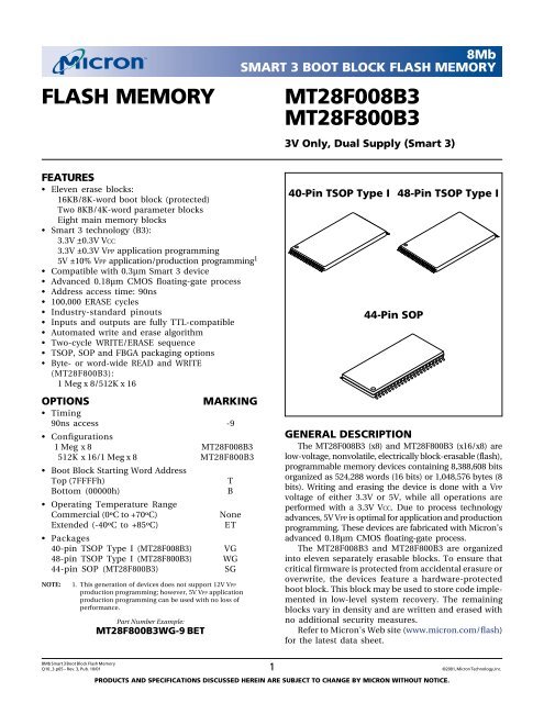
FLASH MEMORY8MbSMART 3 BOOT BLOCK FLASH MEMORYMT28F008B3MT28F800B33V Only, Dual Supply (Smart 3)FEATURES• Eleven erase blocks:16KB/8K-word boot block (protected)Two 8KB/4K-word parameter blocksEight main memory blocks• Smart 3 technology (B3):3.3V ±0.3V VCC3.3V ±0.3V VPP application programming5V ±10% VPP application/production programming 1• Compatible with 0.3µm Smart 3 device• Advanced 0.18µm CMOS floating-gate process• Address access time: 90ns• 100,000 ERASE cycles• Industry-standard pinouts• Inputs and outputs are fully TTL-compatible• Automated write and erase algorithm• Two-cycle WRITE/ERASE sequence• TSOP, SOP and FBGA packaging options• Byte- or word-wide READ and WRITE(MT28F800B3):1 Meg x 8/512K x 16OPTIONSMARKING• Timing90ns access -9• Configurations1 Meg x 8 MT28F008B3512K x 16/1 Meg x 8MT28F800B3• Boot Block Starting Word AddressTop (7FFFFh)TBottom (00000h)B• Operating Temperature RangeCommercial (0ºC to +70ºC)NoneExtended (-40ºC to +85ºC)ET• Packages40-pin TSOP Type I (MT28F008B3) VG48-pin TSOP Type I (MT28F800B3) WG44-pin SOP (MT28F800B3)SGNOTE:1. This generation of devices does not support 12V VPPproduction programming; however, 5V VPP applicationproduction programming can be used with no loss ofperformance.Part Number Example:MT28F800B3WG-9 BET40-Pin TSOP Type I 48-Pin TSOP Type I44-Pin SOPGENERAL DESCRIPTIONThe MT28F008B3 (x8) and MT28F800B3 (x16/x8) arelow-voltage, nonvolatile, electrically block-erasable (flash),programmable memory devices containing 8,388,608 bitsorganized as 524,288 words (16 bits) or 1,048,576 bytes (8bits). Writing and erasing the device is done with a VPPvoltage of either 3.3V or 5V, while all operations areperformed with a 3.3V VCC. Due to process technologyadvances, 5V VPP is optimal for application and productionprogramming. These devices are fabricated with <strong>Micron</strong>’sadvanced 0.18µm CMOS floating-gate process.The MT28F008B3 and MT28F800B3 are organizedinto eleven separately erasable blocks. To ensure thatcritical firmware is protected from accidental erasure oroverwrite, the devices feature a hardware-protectedboot block. This block may be used to store code implementedin low-level system recovery. The remainingblocks vary in density and are written and erased withno additional security measures.Refer to <strong>Micron</strong>’s Web site (www.micron.com/flash)for the latest data sheet.8Mb Smart 3 Boot Block Flash MemoryQ10_3.p65 – Rev. 3, Pub. 10/011PRODUCTS AND SPECIFICATIONS DISCUSSED HEREIN ARE SUBJECT TO CHANGE BY MICRON WITHOUT NOTICE.©2001, <strong>Micron</strong> Technology, Inc.
8MbSMART 3 BOOT BLOCK FLASH MEMORY48-Pin TSOP Type IPIN ASSIGNMENT (Top View)44-Pin SOPA15A14A13A12A11A10A9A8NCNCWE#RP#VPPWP#NCA18A17A7A6A5A4A3A2A1123456789101112131415161718192021222324484746454443424140393837363534333231302928272625A16BYTE#VSSDQ15/(A - 1)DQ7DQ14DQ6DQ13DQ5DQ12DQ4VCCDQ11DQ3DQ10DQ2DQ9DQ1DQ8DQ0OE#VSSCE#A0ORDER NUMBER AND PART MARKINGMT28F800B3WG-9 BMT28F800B3WG-9 TMT28F800B3WG-9 BETMT28F800B3WG-9 TETVPPA18A17A7A6A5A4A3A2A1A0CE#VSSOE#DQ0DQ8DQ1DQ9DQ2DQ10DQ3DQ111234567891011121314151617181920212244434241403938373635343332313029282726252423RP#WE#A8A9A10A11A12A13A14A15A16BYTE#VSSDQ15/(A - 1)DQ7DQ14DQ6DQ13DQ5DQ12DQ4VCCORDER NUMBER AND PART MARKINGMT28F800B3SG-9 BMT28F800B3SG-9 TMT28F800B3SG-9 BETMT28F800B3SG-9 TET40-Pin TSOP Type IA16A15A14A13A12A11A9A8WE#RP#VPPWP#A18A7A6A5A4A3A2A112345678910111213141516171819204039383736353433323130292827262524232221A17VSSNCA19A10DQ7DQ6DQ5DQ4VCCVCCNCDQ3DQ2DQ1DQ0OE#VSSCE#A0ORDER NUMBER AND PART MARKINGMT28F008B3VG-9 BMT28F008B3VG-9 TMT28F008B3VG-9 BETMT28F008B3VG-9 TET8Mb Smart 3 Boot Block Flash MemoryQ10_3.p65 – Rev. 3, Pub. 10/012<strong>Micron</strong> Technology, Inc., reserves the right to change products or specifications without notice.©2001, <strong>Micron</strong> Technology, Inc.
8Mb Smart 3 Boot Block Flash Memory <strong>Micron</strong> Technology, Inc., reserves the right to change products or specifications without notice.Q10_3.p65 – Rev. 3, Pub. 10/01 3©2001, <strong>Micron</strong> Technology, Inc.BYTE# 2A0–A18/(A19)NOTE:WP# 1CE#OE#WE#RP#VCCVPPI/OControlLogicA9CommandExecutionLogicAddr.Buffer/LatchPower(Current)Control1. Does not apply to MT28F800B3SG.2. Does not apply to MT28F008B3.19 (20)FUNCTIONAL BLOCK DIAGRAMAddr.CounterStateMachineVPPSwitch/PumpStatusRegister9(10)10IdentificationRegisterX - Decoder/Block Erase ControlY -Decoder16KB Boot Block8KB Parameter Block8KB Parameter Block96KB Main Block128KB Main Block128KB Main Block128KB Main Block128KB Main Block128KB Main Block128KB Main Block128KB Main BlockY - Select GatesSense AmplifiersWrite/Erase-BitCompare and VerifyDQ15788Input DataLatch/Mux16MUX87A-1InputBufferInputBufferInputBufferOutputBufferOutputBufferOutputBuffer78DQ15/(A - 1) 2DQ8–DQ14 2DQ0–DQ78MbSMART 3 BOOT BLOCK FLASH MEMORY
8MbSMART 3 BOOT BLOCK FLASH MEMORYPIN DESCRIPTIONS44-PIN SOP 40-PIN TSOP 48-PIN TSOPNUMBERS NUMBERS NUMBERS SYMBOL TYPE DESCRIPTION43 9 11 WE# Input Write Enable: Determines if a given cycle is a WRITE cycle. IfWE# is LOW, the cycle is either a WRITE to the commandexecution logic (CEL) or to the memory array.– 12 14 WP# Input Write Protect: Unlocks the boot block when HIGH if VPP =VPPH1 (3.3V) or VPPH2 (5V) and RP# = VIH during a WRITE orERASE. Does not affect WRITE or ERASE operation on otherblocks.12 22 26 CE# Input Chip Enable: Activates the device when LOW. When CE# isHIGH, the device is disabled and goes into standby powermode.44 10 12 RP# Input Reset/Power-Down: When LOW, RP# clears the status register,sets the internal state machine (ISM) to the array read modeand places the device in deep power-down mode. All inputs,including CE#, are “Don’t Care,” and all outputs are High-Z.RP# unlocks the boot block and overrides the condition ofWP# when at VHH (12V), and must be held at VIH during allother modes of operation.14 24 28 OE# Input Output Enable: Enables data output buffers when LOW.When OE# is HIGH, the output buffers are disabled.33 – 47 BYTE# Input Byte Enable: If BYTE# = HIGH, the upper byte is active throughDQ8–DQ15. If BYTE# = LOW, DQ8–DQ14 are High-Z, and alldata is accessed through DQ0–DQ7. DQ15/(A - 1) becomes theleast significant address input.11, 10, 9, 8, 21, 20, 19, 18, 25, 24, 23, A0–A18/ Input Address Inputs: Select a unique 16-bit word or 8-bit byte. The7, 6, 5, 4, 42, 17, 16, 15, 14, 22, 21, 20, (A19) DQ15/(A - 1) input becomes the lowest order address when41, 40, 39, 8, 7, 36, 6, 5, 19, 18, 8, 7, BYTE# = LOW (MT28F800B3) to allow for a selection of an 8-38, 37, 36, 4, 3, 2, 1, 40, 6, 5, 4, 3, 2, bit byte from the 1,048,576 available.35, 34, 3, 2 13, 37 1, 48, 17, 1631 – 45 DQ15/ Input/ Data I/O: MSB of data when BYTE# = HIGH. Address Input: LSB(A - 1) Output of address input when BYTE# = LOW during READ or WRITEoperation.15, 17, 19, 25, 26, 27, 29, 31, 33, DQ0– Input/ Data I/Os: Data output pins during any READ operation or21, 24, 26, 28, 32, 33, 35, 38, 40, DQ7 Output data input pins during a WRITE. These pins are used to input28, 30 34, 35 42, 44 commands to the CEL.16, 18, 20, – 30, 32, 34, DQ8– Input/ Data I/Os: Data output pins during any READ operation or22, 25, 27, 36, 39, 41, DQ14 Output data input pins during a WRITE when BYTE# = HIGH. These29 43 pins are High-Z when BYTE# is LOW.1 11 13 VPP Supply Write/Erase Supply Voltage: From a WRITE or ERASE CONFIRMuntil completion of the WRITE or ERASE, VPP must be at VPPH1(3.3V) or VPPH2 (5V). VPP = “Don’t Care” during all otheroperations.23 30, 31 37 VCC Supply Power Supply: +3.3V ±0.3V.13, 32 23, 39 27, 46 VSS Supply Ground.– 29, 38 9, 10, 15 NC – No Connect: These pins may be driven or left unconnected.8Mb Smart 3 Boot Block Flash MemoryQ10_3.p65 – Rev. 3, Pub. 10/014<strong>Micron</strong> Technology, Inc., reserves the right to change products or specifications without notice.©2001, <strong>Micron</strong> Technology, Inc.
8MbSMART 3 BOOT BLOCK FLASH MEMORYTRUTH TABLE (MT28F800B3) 1FUNCTION RP# CE# OE# WE# WP# BYTE# A0 A9 VPP DQ0–DQ7 DQ8–DQ14 DQ15/A - 1Standby H H X X X X X X X High-Z High-Z High-ZRESET L X X X X X X X X High-Z High-Z High-ZREADREAD (word mode) H L L H X H X X X Data-Out Data-Out Data-OutREAD (byte mode) H L L H X L X X X Data-Out High-Z A-1Output Disable H L H H X X X X X High-Z High-Z High-ZWRITE/ERASE (EXCEPT BOOT BLOCK) 2ERASE SETUP H L H L X X X X X 20h X XERASE CONFIRM 3 H L H L X X X X VPPH D0h X XWRITE SETUP H L H L X X X X X 10h/40h X XWRITE (word mode) 4 H L H L X H X X VPPH Data-In Data-In Data-InWRITE (byte mode) 4 H L H L X L X X VPPH Data-In X A-1READ ARRAY 5 H L H L X X X X X FFh X XWRITE/ERASE (BOOT BLOCK) 2, 7ERASE SETUP H L H L X X X X X 20h X XERASE CONFIRM 3 VHH L H L X X X X VPPH D0h X XERASE CONFIRM 3, 6 H L H L H X X X VPPH D0h X XWRITE SETUP H L H L X X X X X 10h/40h X XWRITE (word mode) 4 VHH L H L X H X X VPPH Data-In Data-In Data-InWRITE (word mode) 4, 6 H L H L H H X X VPPH Data-In Data-In Data-InWRITE (byte mode) 4 VHH L H L X L X X VPPH Data-In X A-1WRITE (byte mode) 4, 6 H L H L H L X X VPPH Data-In X A-1READ ARRAY 5 H L H L X X X X X FFh X XDEVICE IDENTIFICATION 8, 9Manufacturer Compatibility H L L H X H L VID X 89h 00h –(word mode) 10Manufacturer Compatibility H L L H X L L VID X 89h High-Z X(byte mode)Device (word mode, top boot) 10 H L L H X H H VID X 9Ch 88h –Device (byte mode, top boot) H L L H X L H VID X 9Ch High-Z XDevice (word mode, bottom boot) 10 H L L H X H H VID X 9Dh 88h –Device (byte mode, bottom boot) H L L H X L H VID X 9Dh High-Z XNOTE:1. L = VIL (LOW), H = VIH (HIGH), X = VIL or VIH (“Don’t Care”).2. VPPH = VPPH1 = 3.3V or VPPH2 = 5V.3. Operation must be preceded by ERASE SETUP command.4. Operation must be preceded by WRITE SETUP command.5. The READ ARRAY command must be issued before reading the array after writing or erasing.6. When WP# = VIH, RP# may be at VIH or VHH.7. VHH = 12V.8. VID = 12V; may also be read by issuing the IDENTIFY DEVICE command.9. A1–A8, A10–A18 = VIL.10. Value reflects DQ8–DQ15.8Mb Smart 3 Boot Block Flash MemoryQ10_3.p65 – Rev. 3, Pub. 10/015<strong>Micron</strong> Technology, Inc., reserves the right to change products or specifications without notice.©2001, <strong>Micron</strong> Technology, Inc.
8MbSMART 3 BOOT BLOCK FLASH MEMORYwhile the ISM is active. However, there are restrictionson what commands are allowed in this condition. Seethe Command Execution section for more detail.DEEP POWER-DOWN MODETo allow for maximum power conservation, theMT28F800B3 and MT28F008B3 feature a very low current,deep power-down mode. To enter this mode, theRP# pin is taken to VSS ±0.2V. In this mode, the currentdraw is a maximum of 8µA at 3.3V VCC. Entering deeppower-down also clears the status register and sets theISM to the read array mode.MEMORY ARCHITECTUREThe MT28F800B3 and MT28F008B3 memory arrayarchitecture is designed to allow sections to be erasedwithout disturbing the rest of the array. The array isdivided into eleven addressable blocks that vary in sizeand are independently erasable. When blocks rather thanthe entire array are erased, total device endurance isenhanced, as is system flexibility. Only the ERASE functionis block-oriented. All READ and WRITE operationsare done on a random-access basis.The boot block is protected from unintentional ERASEor WRITE with a hardware protection circuit which requiresthat a super-voltage be applied to RP# or that theWP# pin be driven HIGH before erasure is commenced.The boot block is intended for the core firmware requiredfor basic system functionality. The remaining ten blocksdo not require that either of these two conditions be metbefore WRITE or ERASE operations.BOOT BLOCKThe hardware-protected boot block provides extrasecurity for the most sensitive portions of the firmware.This 16KB block may only be erased or written when theRP# pin is at the specified boot block unlock voltage (VHH)of 12V or when the WP# pin is HIGH. During a WRITE orERASE of the boot block, the RP# pin must be held at VHHor the WP# pin held HIGH until the WRITE or ERASE iscompleted. (The WP# pin does not apply to the SOPpackage.) The VPP pin must be at VPPH (3.3V or 5V) whenthe boot block is written to or erased.Figure 1Memory Address MapsWORD ADDRESSBYTE ADDRESSWORD ADDRESSBYTE ADDRESS7FFFFh70000h6FFFFh60000h5FFFFh50000h4FFFFh40000h3FFFFh30000h2FFFFh20000h1FFFFh10000h0FFFFh04000h03FFFh03000h02FFFh02000h01FFFh00000hFFFFFhE0000hDFFFFhC0000hBFFFFhA0000h9FFFFh80000h7FFFFh60000h5FFFFh40000h3FFFFh20000h1FFFFh08000h07FFFh06000h05FFFh04000h03FFFh00000h128KB Main Block128KB Main Block128KB Main Block128KB Main Block128KB Main Block128KB Main Block128KB Main Block96KB Main Block8KB Parameter Block8KB Parameter Block16KB Boot Block7FFFFh7E000h7DFFFh7D000h7CFFFh7C000h7BFFFh70000h6FFFFh60000h5FFFFh50000h4FFFFh40000h3FFFFh30000h2FFFFh20000h1FFFFh10000h0FFFFh00000hFFFFFhFC000hFBFFFhFA000hF9FFFhF8000hF7FFFhE0000hDFFFFhC0000hBFFFFhA0000h9FFFFh80000h7FFFFh60000h5FFFFh40000h3FFFFh20000h1FFFFh00000h16KB Boot Block8KB Parameter Block8KB Parameter Block96KB Main Block128KB Main Block128KB Main Block128KB Main Block128KB Main Block128KB Main Block128KB Main Block128KB Main BlockBottom BootMT28F008B3/800B3xx-xxBTop BootMT28F008B3/800B3xx-xxT8Mb Smart 3 Boot Block Flash MemoryQ10_3.p65 – Rev. 3, Pub. 10/018<strong>Micron</strong> Technology, Inc., reserves the right to change products or specifications without notice.©2001, <strong>Micron</strong> Technology, Inc.
8MbSMART 3 BOOT BLOCK FLASH MEMORYThe MT28F800B3 and MT28F008B3 are available intwo configurations and top or bottom boot block. The topboot block version supports processors of the x86 variety.The bottom boot block version is intended for 680X0 andRISC applications. Figure 1 illustrates the memory addressmaps associated with these two versions.PARAMETER BLOCKSThe two 8KB parameter blocks store less sensitive andmore frequently changing system parameters and alsomay store configuration or diagnostic coding. Theseblocks are enabled for erasure when the VPP pin is at VPPH.No super-voltage unlock or WP# control is required.MAIN MEMORY BLOCKSThe eight remaining blocks are general-purposememory blocks and do not require a super-voltage onRP# or WP# control to be erased or written. These blocksare intended for code storage, ROM-resident applicationsor operating systems that require in-system updatecapability.OUTPUT (READ) OPERATIONSThe MT28F800B3 and MT28F008B3 feature three differenttypes of READs. Depending on the current mode ofthe device, a READ operation produces data from thememory array, status register or device identificationregister. In each of these three cases, the WE#, CE# andOE# inputs are controlled in a similar manner. Movingbetween modes to perform a specific READ is describedin the Command Execution section.MEMORY ARRAYTo read the memory array, WE# must be HIGH, andOE# and CE# must be LOW. Valid data is output on theDQ pins when these conditions have been met, and avalid address is given. Valid data remains on the DQ pinsuntil the address changes, or until OE# or CE# goes HIGH,whichever occurs first. The DQ pins continue to outputnew data after each address transition as long as OE# andCE# remain LOW.The MT28F800B3 features selectable bus widths.When the memory array is accessed as a 512K x 16, BYTE#is HIGH, and data is output on DQ0–DQ15. To access thememory array as a 1 Meg x 8, BYTE# must be LOW, DQ8–DQ14 must be High-Z, and all data must be output onDQ0–DQ7. The DQ15/(A - 1) pin becomes the lowestorder address input so that 1,048,576 locations can beread.After power-up or RESET, the device is automaticallyin the array read mode. All commands and their operationsare covered in the Command Set and CommandExecution sections.STATUS REGISTERPerforming a READ of the status register requiresthe same input sequencing as a READ of the arrayexcept that the address inputs are “Don’t Care.” Thestatus register contents are always output on DQ0–DQ7, regardless of the condition of BYTE# on theMT28F800B3. DQ8–DQ15 are LOW when BYTE# isHIGH, and DQ8–DQ14 are High-Z when BYTE# is LOW.Data from the status register is latched on the fallingedge of OE# or CE#, whichever occurs last. If the contentsof the status register change during a READ of thestatus register, either OE# or CE# may be toggled whilethe other is held LOW to update the output.Following a WRITE or ERASE, the device automaticallyenters the status register read mode. In addition, aREAD during a WRITE or ERASE produces the statusregister contents on DQ0–DQ7. When the device is in theerase suspend mode, a READ operation produces thestatus register contents until another command is issued.In certain other modes, READ STATUS REGISTERmay be given to return to the status register read mode.All commands and their operations are described in theCommand Set and Command Execution sections.IDENTIFICATION REGISTERA READ of the two 8-bit device identification registersrequires the same input sequencing as a READ of thearray. WE# must be HIGH, and OE# and CE# must beLOW. However, ID register data is output only on DQ0–DQ7, regardless of the condition of BYTE# on theMT28F800B3. A0 is used to decode between the two bytesof the device ID register; all other address inputs are“Don’t Care.” When A0 is LOW, the manufacturer compatibilityID is output, and when A0 is HIGH, the deviceID is output. DQ8–DQ15 are High-Z when BYTE# is LOW.When BYTE# is HIGH, DQ8–DQ15 are 00h when themanufacturer compatibility ID is read and 88h when thedevice ID is read.To get to the identification register read mode, READIDENTIFICATION may be issued while the device is incertain other modes. In addition, the identification registerread mode can be reached by applying a super-voltage(VID) to the A9 pin. Using this method, the ID registercan be read while the device is in any mode. When A9 isreturned to VIL or VIH, the device returns to the previousmode.INPUT OPERATIONSThe DQ pins are used either to input data to the arrayor to input a command to the CEL. A command inputissues an 8-bit command to the CEL to control the modeof operation of the device. A WRITE is used to inputdata to the memory array. The following section de-8Mb Smart 3 Boot Block Flash MemoryQ10_3.p65 – Rev. 3, Pub. 10/019<strong>Micron</strong> Technology, Inc., reserves the right to change products or specifications without notice.©2001, <strong>Micron</strong> Technology, Inc.
8MbSMART 3 BOOT BLOCK FLASH MEMORYscribes both types of inputs. More information describinghow to use the two types of inputs to write or erasethe device is provided in the Command Execution section.COMMANDSTo perform a command input, OE# must be HIGH,and CE# and WE# must be LOW. Addresses are “Don’tCare” but must be held stable, except during an ERASECONFIRM (described in a later section). The 8-bit commandis input on DQ0–DQ7, while DQ8–DQ15 are “Don’tCare” on the MT28F800B3. The command is latched onthe rising edge of CE# (CE#-controlled) or WE# (WE#-controlled), whichever occurs first. The condition ofBYTE# on the MT28F800B3 has no effect on a commandinput.MEMORY ARRAYA WRITE to the memory array sets the desired bits tologic 0s but cannot change a given bit to a logic 1 from alogic 0. Setting any bits to a logic 1 requires that the entireblock be erased. To perform a WRITE, OE# must be HIGH,CE# and WE# must be LOW, and VPP must be set to VPPH1or VPPH2. Writing to the boot block also requires that theRP# pin be at VHH or WP# be HIGH. A0–A18 (A19) providethe address to be written, while the data to bewritten to the array is input on the DQ pins. The dataand addresses are latched on the rising edge of CE#(CE#-controlled) or WE# (WE#-controlled), whicheveroccurs first. A WRITE must be preceded by a WRITESETUP command. Details on how to input data to thearray are described in the Write Sequence section.Selectable bus sizing applies to WRITEs as it does toREADs on the MT28F800B3. When BYTE# is LOW (bytemode), data is input on DQ0–DQ7, DQ8–DQ14 are High-Z, and DQ15 becomes the lowest order address input.When BYTE# is HIGH (word mode), data is input on DQ0–DQ15.COMMAND SETTo simplify writing of the memory blocks, theMT28F800B3 and MT28F008B3 incorporate an ISM thatcontrols all internal algorithms for writing and erasingthe floating gate memory cells. An 8-bit command set isused to control the device. Details on how to sequencecommands are provided in the Command Executionsection. Table 1 lists the valid commands.Table 1Command SetCOMMAND HEX CODE DESCRIPTIONRESERVED 00h This command and all unlisted commands are invalid and should notbe called. These commands are reserved to allow for future featureenhancements.READ ARRAY FFh Must be issued after any other command cycle before the array can beread. It is not necessary to issue this command after power-up or RESET.IDENTIFY DEVICE 90h Allows the device and manufacturer compatibility ID to be read. A0 isused to decode between the manufacturer compatibility ID (A0 = LOW)and device ID (A0 = HIGH).READ STATUS REGISTER 70h Allows the status register to be read. Please refer to Table 2 for moreinformation on the status register bits.CLEAR STATUS REGISTER 50h Clears status register bits 3-5, which cannot be cleared by the ISM.ERASE SETUP 20h The first command given in the two-cycle ERASE sequence. The ERASE isnot completed unless followed by ERASE CONFIRM.ERASE CONFIRM/RESUME D0h The second command given in the two-cycle ERASE sequence. Must followan ERASE SETUP command to be valid. Also used during an ERASESUSPEND to resume the ERASE.WRITE SETUP 40h or The first command given in the two-cycle WRITE sequence. The write10h data and address are given in the following cycle to complete the WRITE.ERASE SUSPEND B0h Requests a halt of the ERASE and puts the device into the erase suspendmode. When the device is in this mode, only READ STATUS REGISTER,READ ARRAY and ERASE RESUME commands may be executed.8Mb Smart 3 Boot Block Flash MemoryQ10_3.p65 – Rev. 3, Pub. 10/0110<strong>Micron</strong> Technology, Inc., reserves the right to change products or specifications without notice.©2001, <strong>Micron</strong> Technology, Inc.
8MbSMART 3 BOOT BLOCK FLASH MEMORYISM STATUS REGISTERThe 8-bit ISM status register (see Table 2) is polledto check for WRITE or ERASE completion or any relatederrors. During or following a WRITE, ERASE or ERASESUSPEND, a READ operation outputs the status registercontents on DQ0–DQ7 without prior command. Whilethe status register contents are read, the outputs are notbe updated if there is a change in the ISM status unlessOE# or CE# is toggled. If the device is not in the write,erase, erase suspend or status register read mode, READSTATUS REGISTER (70h) can be issued to view the statusregister contents.All of the defined bits are set by the ISM, but onlythe ISM and erase suspend status bits are reset by theISM. The erase, write and VPP status bits must be clearedusing CLEAR STATUS REGISTER. If the VPP status bit(SR3) is set, the CEL does not allow further WRITE orERASE operations until the status register is cleared.This enables the user to choose when to poll and clearthe status register. For example, the host system mayperform multiple BYTE WRITE operations before checkingthe status register instead of checking after eachindividual WRITE. Asserting the RP# signal or poweringdown the device also clears the status register.Table 2Status Register Bit DefinitionsISMS ESS ES WS VPPS R7 6 5 4 3 2–0STATUSBIT # STATUS REGISTER BIT DESCRIPTIONSR7 ISM STATUS (ISMS) The ISMS bit displays the active status of the state machine during1 = Ready WRITE or BLOCK ERASE operations. The controlling logic polls this0 = Busy bit to determine when the erase and write status bits are valid.SR6 ERASE SUSPEND STATUS (ESS) Issuing an ERASE SUSPEND places the ISM in the suspend mode1 = ERASE suspended and sets this and the ISMS bit to “1.” The ESS bit remains “1”0 = ERASE in progress/completed until an ERASE RESUME is issued.SR5 ERASE STATUS (ES) ES is set to “1” after the maximum number of ERASE cycles is1 = BLOCK ERASE error executed by the ISM without a successful verify. ES is only cleared0 = Successful BLOCK ERASE by a CLEAR STATUS REGISTER command or after a RESET.SR4 WRITE STATUS (WS) WS is set to “1” after the maximum number of WRITE cycles is1 = WORD/BYTE WRITE error executed by the ISM without a successful verify. WS is only cleared0 = Successful WORD/BYTE WRITE by a CLEAR STATUS REGISTER command or after a RESET.SR3 VPP STATUS (VPPS) VPPS detects the presence of a VPP voltage. It does not monitor VPP1 = No VPP voltage detected continuously, nor does it indicate a valid VPP voltage. The VPP pin0 = VPP present is sampled for 3.3V or 5V after WRITE or ERASE CONFIRM is given.VPPS must be cleared by CLEAR STATUS REGISTER or by a RESET.SR0-2 RESERVED Reserved for future use.8Mb Smart 3 Boot Block Flash MemoryQ10_3.p65 – Rev. 3, Pub. 10/0111<strong>Micron</strong> Technology, Inc., reserves the right to change products or specifications without notice.©2001, <strong>Micron</strong> Technology, Inc.
8MbSMART 3 BOOT BLOCK FLASH MEMORYCOMMAND EXECUTIONCommands are issued to bring the device into differentoperational modes. Each mode allows specific operationsto be performed. Several modes require a sequenceof commands to be written before they are reached. Thefollowing section describes the properties of each mode,and Table 3 lists all command sequences required toperform the desired operation.READ ARRAYThe array read mode is the initial state of the deviceupon power-up and after a RESET. If the device is in anyother mode, READ ARRAY (FFh) must be given to returnto the array read mode. Unlike the WRITE SETUP command(40h), READ ARRAY does not need to be givenbefore each individual READ access.IDENTIFY DEVICEIDENTIFY DEVICE (90h) may be written to the CEL toenter the identify device mode. While the device is in thismode, any READ produces the device identification whenA0 is HIGH and the manufacturer compatibility identificationwhen A0 is LOW. The device remains in this modeuntil another command is given.WRITE SEQUENCETwo consecutive cycles are needed to input data tothe array. WRITE SETUP (40h or 10h) is given in the firstcycle. The next cycle is the WRITE, during which the writeaddress and data are issued and VPP is brought to VPPH.Writing to the boot block also requires that the RP# pin bebrought to VHH or the WP# pin be brought HIGH at thesame time VPP is brought to VPPH. The ISM now begins towrite the word or byte. VPP must be held at VPPH until theWRITE is completed (SR7 = 1).While the ISM executes the WRITE, the ISM status bit(SR7) is at 0, and the device does not respond to anycommands. Any READ operation produces the statusregister contents on DQ0–DQ7. When the ISM status bit(SR7) is set to a logic 1, the WRITE has been completed,and the device goes into the status register read modeuntil another command is given.After the ISM has initiated the WRITE, it cannot beaborted except by a RESET or by powering down the part.Doing either during a WRITE corrupts the data beingwritten. If only the WRITE SETUP command has beengiven, the WRITE may be nullified by performing a nullWRITE. To execute a null WRITE, FFh must be writtenTable 3Command SequencesBUS FIRST SECONDCYCLES CYCLE CYCLECOMMANDS REQ’D OPERATION ADDRESS DATA OPERATION ADDRESS DATA NOTESREAD ARRAY 1 WRITE X FFh 1IDENTIFY DEVICE 3 WRITE X 90h READ IA ID 2, 3READ STATUS REGISTER 2 WRITE X 70h READ X SRD 4CLEAR STATUS REGISTER 1 WRITE X 50hERASE SETUP/CONFIRM 2 WRITE X 20h WRITE BA D0h 5, 6ERASE SUSPEND/RESUME 2 WRITE X B0h WRITE X D0hWRITE SETUP/WRITE 2 WRITE X 40h WRITE WA WD 6, 7ALTERNATE WORD/BYTE 2 WRITE X 10h WRITE WA WD 6, 7WRITENOTE:1. Must follow WRITE or ERASE CONFIRM commands to the CEL in order to enable Flash array READ cycles.2. IA = Identify Address: 00h for manufacturer compatibility ID; 01h for device ID.3. ID = Identify Data.4. SRD = Status Register Data.5. BA = Block Address (A12–A19).6. Addresses are “Don’t Care” in first cycle but must be held stable.7. WA = Address to be written; WD = Data to be written to WA.8Mb Smart 3 Boot Block Flash MemoryQ10_3.p65 – Rev. 3, Pub. 10/0112<strong>Micron</strong> Technology, Inc., reserves the right to change products or specifications without notice.©2001, <strong>Micron</strong> Technology, Inc.
8MbSMART 3 BOOT BLOCK FLASH MEMORYwhen BYTE# is LOW, or FFFFh must be written whenBYTE# is HIGH. When the ISM status bit (SR7) has beenset, the device is in the status register read mode untilanother command is issued.ERASE SEQUENCEExecuting an ERASE sequence sets all bits within ablock to logic 1. The command sequence necessary toexecute an ERASE is similar to that of a WRITE. To provideadded security against accidental block erasure,two consecutive command cycles are required to initiatean ERASE of a block. In the first cycle, addresses are“Don’t Care,” and ERASE SETUP (20h) is given. In thesecond cycle, VPP must be brought to VPPH, an addresswithin the block to be erased must be issued, and ERASECONFIRM (D0h) must be given. If a command other thanERASE CONFIRM is given, the write and erase status bits(SR4 and SR5) are set, and the device is in the statusregister read mode.After the ERASE CONFIRM (D0h) is issued, the ISMstarts the ERASE of the addressed block. Any READoperation outputs the status register contents on DQ0–DQ7. VPP must be held at VPPH until the ERASE is completed(SR7 = 1). When the ERASE is completed, thedevice is in the status register read mode until anothercommand is issued. Erasing the boot block also requiresthat either the RP# pin be set to VHH or the WP# pin beheld HIGH at the same time VPP is set to VPPH.ERASE SUSPENSIONThe only command that may be issued while anERASE is in progress is ERASE SUSPEND. This commandenables other commands to be executed whilepausing the ERASE in progress. When the device hasreached the erase suspend mode, the erase suspendstatus bit (SR6) and ISM status bit (SR7) are set. Thedevice may now be given a READ ARRAY, ERASE RE-SUME or READ STATUS REGISTER command. AfterREAD ARRAY has been issued, any location not withinthe block being erased may be read. If ERASE RESUMEis issued before SR6 has been set, the device immediatelyproceeds with the ERASE in progress.ERROR HANDLINGAfter the ISM status bit (SR7) has been set, the VPP(SR3), write (SR4) and erase (SR5) status bits may bechecked. If one or a combination of these three bits hasbeen set, an error has occurred. The ISM cannot resetthese three bits. To clear these bits, CLEAR STATUS REG-ISTER (50h) must be given. If the VPP status bit (SR3) is set,further WRITE or ERASE operations cannot resume untilthe status register is cleared. Table 4 lists the combinationof errors.Table 4Status Register Error Code Description 1STATUS BITSSR5 SR4 SR3 ERROR DESCRIPTION0 0 0 No errors0 0 1 VPP voltage error0 1 0 WRITE error0 1 1 WRITE error, VPP voltage not valid at time of WRITE1 0 0 ERASE error1 0 1 ERASE error, VPP voltage not valid at time of ERASE CONFIRM1 1 0 Command sequencing error or WRITE/ERASE error1 1 1 Command sequencing error, VPP voltage error, with WRITE and ERASE errorsNOTE:1. SR3-SR5 must be cleared using CLEAR STATUS REGISTER.8Mb Smart 3 Boot Block Flash MemoryQ10_3.p65 – Rev. 3, Pub. 10/0113<strong>Micron</strong> Technology, Inc., reserves the right to change products or specifications without notice.©2001, <strong>Micron</strong> Technology, Inc.
8MbSMART 3 BOOT BLOCK FLASH MEMORYSELF-TIMED WRITE SEQUENCE(WORD OR BYTE WRITE) 1COMPLETE WRITE STATUS-CHECKSEQUENCEStartStart (WRITE completed)WRITE 40h or 10hSR3 = 0?NOVPP4, 5ErrorYESVPP = 3.3V or 5VSR4 = 0?NOBYTE/WORD WRITE Error 5YESWRITE Word or ByteAddress/DataWRITE SuccessfulSTATUS REGISTERREADSR7 = 1?NOYESComplete Status2Check (optional)WRITE Complete 3NOTE:1. Sequence may be repeated for additional BYTE or WORD WRITEs.2. Complete status check is not required. However, if SR3 = 1, further WRITEs are inhibited until the status register iscleared.3. Device will be in status register read mode. To return to the array read mode, the FFh command must be issued.4. If SR3 is set during a WRITE or BLOCK ERASE attempt, CLEAR STATUS REGISTER must be issued before further WRITEor ERASE operations are allowed by the CEL.5. Status register bits 3-5 must be cleared using CLEAR STATUS REGISTER.8Mb Smart 3 Boot Block Flash MemoryQ10_3.p65 – Rev. 3, Pub. 10/0115<strong>Micron</strong> Technology, Inc., reserves the right to change products or specifications without notice.©2001, <strong>Micron</strong> Technology, Inc.
8MbSMART 3 BOOT BLOCK FLASH MEMORYSELF-TIMED BLOCK ERASE SEQUENCE 1StartCOMPLETE BLOCK ERASESTATUS-CHECK SEQUENCEStart (ERASE completed)WRITE 20hSR3 = 0?NOVPPError5, 6YESVPP = 3.3V or 5VSR4, 5 = 1?YESCommand Sequence Error6WRITE D0h,Block AddressNOSR5 = 0?NOBLOCK ERASE Error6STATUS REGISTERREADERASEBusyYESERASE SuccessfulSR7 = 1?NONOSuspend ERASE?YESComplete Status2Check (optional)YESSuspend 4SequenceERASE Complete 3ERASE ResumedNOTE:1. Sequence may be repeated to erase additional blocks.2. Complete status check is not required. However, if SR3 = 1, further ERASEs are inhibited until the status register iscleared.3. To return to the array read mode, the FFh command must be issued.4. Refer to the ERASE SUSPEND flowchart for more information.5. If SR3 is set during a WRITE or BLOCK ERASE attempt, CLEAR STATUS REGISTER must be issued before further WRITEor ERASE operations are allowed by the CEL.6. Status register bits 3-5 must be cleared using CLEAR STATUS REGISTER.8Mb Smart 3 Boot Block Flash MemoryQ10_3.p65 – Rev. 3, Pub. 10/0116<strong>Micron</strong> Technology, Inc., reserves the right to change products or specifications without notice.©2001, <strong>Micron</strong> Technology, Inc.
8MbSMART 3 BOOT BLOCK FLASH MEMORYERASE SUSPEND/RESUME SEQUENCEStart (ERASE in progress)WRITE B0h(ERASE SUSPEND)VPP = 3.3V or 5VSTATUS REGISTERREADSR7 = 1?NOYESSR6 = 1?NOYESWRITE FFh(READ ARRAY)ERASE CompletedDoneReading?NOYESWRITE D0h(ERASE RESUME)Resume ERASE8Mb Smart 3 Boot Block Flash MemoryQ10_3.p65 – Rev. 3, Pub. 10/0117<strong>Micron</strong> Technology, Inc., reserves the right to change products or specifications without notice.©2001, <strong>Micron</strong> Technology, Inc.
?Foto: SGP. BraunAHA!FrauBeckmannerklärt die Dinge.„RETRO“Folge SECHSSeit mir meine Enkel unter dem Weihnachtsbaumerklären wollten, was alles „retro“ ist, sehe ich viele Dingemit anderen Augen: die Muster auf meinen Küchenschürzen,meine Möbel, mein Geschirr, den alten Kühlschrankvon Onkel Franz im Keller, sogar meinen guten altenApfelkuchen, mein Telefon sowieso – das mit dem Spiralkabel.Ich werde den Verdacht nicht mehr los: Hier, inmeiner guten alten Wohnung, kann er besichtigt werden:der Nabel der RETRO-Welt.Es ist nämlich alles „megatrendy“, was mich umgibt.„Voll fresh, die Oma“ – so hieß es denn auch.Sie merken es sicher schon: Jetzt wird es etwas kompliziert.Es geht nämlich diesmal wirklich um Mode. Das warfrüher immer das Neueste, „der letzte Schrei“. Damitscheint es jetzt aber vorbei zu sein. Ob Autos, Kleidungoder Haarschnitte: Auf unseren Straßen begegnen sichalle Trends mindestens der letzten fünfzig Jahre, allesamtneu aufgegossen und gut durcheinander gerührt. Wenndas mal nicht fad schmeckt. Übrigens: Ich glaube, ichweiß jetzt, was die Dinge „retroreif“ macht: Sie müssenerst mindestens ein Mal so richtig aus der Mode gewesensein, „out“ und „uncool“, wie meine Enkel sagen, „peinlich“,wie ich sage. Dann sind sie oft schneller wieder daals man denkt.Ehrlich gesagt: Ich finde RETRO ziemlich langweilig.Richtig gut sind nämlich – das kann ich mit über Achtzigvielleicht einmal sagen – die Dinge, die immer gut ankamen.Und die gibt es tatsächlich, in aller Bescheidenheit.Streichen Sie bitte ein Beispiel aus der Liste: meinenApfelkuchen!Gertrud Beckmann, 83, Krankenschwester,seit 1943 im Roten Kreuz, unter anderemüber ihre Kinder und Enkel in ständigemKontakt mit der „Szene“, ist für „Gut Leben“als „Trend-Scout“ unentbehrlich.Was ist „amtlich“ und „hip“? Sie hilft unserenLeserinnen und Lesern weiter. Wenn Sie also einaktuelles Modewort, das neueste ComputerspielIhres Enkels oder das „Navi-System“ in derMittelkonsole der Limousine Ihres Neffen verstehenwollen – schreiben Sie an die Redaktion.(Anschrift siehe unten!)Frau Beckmann erklärt es – auf ihre Weise.IMPRESSUMHerausgeber: Ralph HoffertDeutsches Rotes Kreuz HertenGartenstraße 56D-45699 Hertenwww.magazin-gut-leben.deherausgeber@magazin-gut-leben.deRedaktion: Vatter + VatterAgentur f. Werbung & KommunikationIm Blankenfeld 6, D-46238 Bottropwww.vatter-vatter.deredaktion@magazin-gut-leben.deVerantwortlich: Klaus VatterArt-Director: Hans-Hermann BraunGrafik: Arnd Vatter, Kamala GrossartFoto: Photocase.com, Arnd Vatter,Hans-Hermann BraunAnzeigen: Benjamin Loick+49 (0)2366 - 1815 - 130anzeigen@magazin-gut-leben.deHerstellung: Arnd VatterProduktionsmanagement:Vatter + VatterAgentur f. Werbung & KommunikationNachdruck, Aufnahme in Online-Dienste undInternet sowie Vervielfältigung auf Datenträgernsämtlicher Beiträge nur nach vorherigerschriftlicher Genehmigung des Herausgebers.18www.magazin-gut-leben.de
8MbSMART 3 BOOT BLOCK FLASH MEMORYCAPACITANCE(T A = 25ºC; f = 1 MHz)PARAMETER/CONDITION SYMBOL MAX UNITS NOTESInput Capacitance CI 9 pFOutput Capacitance CO 12 pFREAD AND STANDBY CURRENT DRAIN 1Commercial Temperature (0ºC ≤ T A ≤ +70ºC) and Extended Temperature (-40ºC ≤ T A ≤ +85ºC)PARAMETER/CONDITION SYMBOL MAX UNITS NOTESREAD CURRENT: WORD-WIDE(CE# ≤ 0.2V; OE# VCC - 0.2V; f = 5 MHz; ICC1 15 mA 2, 3Other inputs ≤ 0.2V or VCC - 0.2V; RP# VCC - 0.2V)READ CURRENT: BYTE-WIDE(CE# ≤ 0.2V; OE# VCC - 0.2V; f = 5 MHz; ICC2 15 mA 2, 3Other inputs ≤ 0.2V or VCC - 0.2V; RP# = VCC - 0.2V)STANDBY CURRENT: TTL INPUT LEVELSVCC power supply standby current ICC3 2 mA(CE# = RP# = VIH; Other inputs = VIL or VIH)STANDBY CURRENT: CMOS INPUT LEVELSVCC power supply standby current ICC4 100 µA(CE# = RP# = VCC - 0.2V)DEEP POWER-DOWN CURRENT: VCC SUPPLY ICC6 8 µA(RP# = VSS ±0.2V)STANDBY OR READ CURRENT: VPP SUPPLY IPP1 ±15 µA(VPP ≤ 5.5V)DEEP POWER-DOWN CURRENT: VPP SUPPLY IPP2 5 µA(RP# = VSS ±0.2V)NOTE:1. VCC = MAX VCC during ICC tests.2. ICC is dependent on cycle rates.3. ICC is dependent on output loading. Specified values are obtained with the outputs open.8Mb Smart 3 Boot Block Flash MemoryQ10_3.p65 – Rev. 3, Pub. 10/0119<strong>Micron</strong> Technology, Inc., reserves the right to change products or specifications without notice.©2001, <strong>Micron</strong> Technology, Inc.
8MbSMART 3 BOOT BLOCK FLASH MEMORYREAD TIMING PARAMETERSELECTRICAL CHARACTERISTICS AND RECOMMENDED AC OPERATING CONDITIONS 1Commercial Temperature (0ºC ≤ T A ≤ +70ºC) and Extended Temperature (-40ºC ≤ T A ≤ +85ºC); VCC = +3.3V ±0.3VAC CHARACTERISTICS-9/-9 ETPARAMETER SYMBOL MIN MAX UNITS NOTESREAD cycle time t RC 90 nsAccess time from CE# t ACE 90 ns 2Access time from OE# t AOE 40 ns 2Access time from address t AA 90 nsRP# HIGH to output valid delay t RWH 1,000 nsOE# or CE# HIGH to output in High-Z t OD 25 nsOutput hold time from OE#, CE# or address change t OH 0 nsRP# LOW pulse width t RP 150 nsNOTE:1. Measurements tested under AC Test Conditions.2. OE# may be delayed by t ACE minus t AOE after CE# falls before t ACE is affected.AC TEST CONDITIONSInput pulse levels ...................................................... 0V to 3VInput rise and fall times ................................................
8MbSMART 3 BOOT BLOCK FLASH MEMORYWORD-WIDE READ CYCLE 1 VALID DATAA0–A18/(A19)V IHV ILVALID ADDRESSt RCt AACE#V IHV ILt ACEt AOEt ODOE#V IHV ILWE#V IHV ILt OHDQ0–DQ15V IHV ILt RWHRP#V IHVILDON’T CAREUNDEFINEDTIMING PARAMETERSCommercial Temperature (0ºC ≤ T A ≤ +70ºC)Extended Temperature (-40ºC ≤ T A ≤ +85ºC)-9/-9 ETSYMBOL MIN MAX UNITSt RC 90 nst ACE 90 nst AOE 40 nst AA 90 ns-9/-9 ETSYMBOL MIN MAX UNITSt RWH 1,000 nst OD 25 nst OH 0 nsNOTE:1. BYTE# = HIGH (MT28F800B3 only).8Mb Smart 3 Boot Block Flash MemoryQ10_3.p65 – Rev. 3, Pub. 10/0121<strong>Micron</strong> Technology, Inc., reserves the right to change products or specifications without notice.©2001, <strong>Micron</strong> Technology, Inc.
8MbSMART 3 BOOT BLOCK FLASH MEMORYBYTE-WIDE READ CYCLE 1 VALID DATAA0–A18/(A19)V IHV ILVALID ADDRESSt RCt AACE#V IHV ILt ACEt AOEt ODOE#V IHV ILWE#V IHV ILt OHDQ0–DQ7V IHV ILDQ8–DQ14V IHV ILHIGH-Zt RWHRP#V IHV ILDON’T CAREUNDEFINEDTIMING PARAMETERSCommercial Temperature (0ºC ≤ T A ≤ +70ºC)Extended Temperature (-40ºC ≤ T A ≤ +85ºC)-9/-9 ETSYMBOL MIN MAX UNITSt RC 90 nst ACE 90 nst AOE 40 nst AA 90 ns-9/-9 ETSYMBOL MIN MAX UNITSt RWH 1,000 nst OD 25 nst OH 0 nsNOTE:1. BYTE# = LOW (MT28F800B3 only).8Mb Smart 3 Boot Block Flash MemoryQ10_3.p65 – Rev. 3, Pub. 10/0122<strong>Micron</strong> Technology, Inc., reserves the right to change products or specifications without notice.©2001, <strong>Micron</strong> Technology, Inc.
8MbSMART 3 BOOT BLOCK FLASH MEMORYRECOMMENDED DC WRITE/ERASE CONDITIONS 1Commercial Temperature (0ºC ≤ T A ≤ +70ºC) and Extended Temperature (-40ºC ≤ T A ≤ +85ºC); VCC = +3.3V ±0.3VPARAMETER/CONDITION SYMBOL MIN MAX UNITS NOTESVPP WRITE/ERASE lockout voltage VPPLK – 1.5 V 2VPP voltage during WRITE/ERASE operation VPPH1 3.0 3.6 V 3VPP voltage during WRITE/ERASE operation VPPH2 4.5 5.5 VBoot block unlock voltage VHH 10 12.6 VVCC WRITE/ERASE lockout voltage VLKO 2 – VWRITE/ERASE CURRENT DRAIN 4Commercial Temperature (0ºC ≤ T A ≤ +70ºC) and Extended Temperature (-40ºC - T A - +85ºC); VCC = +3.3V ±0.3V3.3V VPP 5V VPPPARAMETER/CONDITION SYMBOL MAX MAX UNITS NOTESWORD WRITE CURRENT: VCC SUPPLY ICC7 20 20 mA 5WORD WRITE CURRENT: VPP SUPPLY IPP3 20 20 mA 5BYTE WRITE CURRENT: VCC SUPPLY ICC8 20 20 mA 6BYTE WRITE CURRENT: VPP SUPPLY IPP4 20 20 mA 6ERASE CURRENT: VCC SUPPLY ICC9 25 25 mAERASE CURRENT: VPP SUPPLY IPP5 25 30 mAERASE SUSPEND CURRENT: VCC SUPPLY ICC10 8 10 mA 7(ERASE suspended)ERASE SUSPEND CURRENT: VPP SUPPLY IPP6 200 200 µA(ERASE suspended)NOTE:1. WRITE operations are tested at VPP voltages equal to or less than the previous ERASE.2. Absolute WRITE/ERASE protection when VPP ≤ VPPLK.3. When 3.3V VCC and VPP are used, VCC cannot exceed VPP by more than 500mV during WRITE and ERASE operations.4. All currents are in RMS unless otherwise noted.5. Applies to MT28F800B3 only.6. Applies to MT28F008B3 and MT28F800B3 with BYTE# = LOW.7. Parameter is specified when device is not accessed. Actual current draw will be ICC10 plus read current if a READ isexecuted while the device is in erase suspend mode.8Mb Smart 3 Boot Block Flash MemoryQ10_3.p65 – Rev. 3, Pub. 10/0123<strong>Micron</strong> Technology, Inc., reserves the right to change products or specifications without notice.©2001, <strong>Micron</strong> Technology, Inc.
8MbSMART 3 BOOT BLOCK FLASH MEMORYSPEED-DEPENDENT WRITE/ERASE AC TIMING CHARACTERISTICS ANDRECOMMENDED AC OPERATING CONDITIONS:WE# (CE#)-CONTROLLED WRITESCommercial Temperature (0ºC ≤ T A ≤ +70ºC) and Extended Temperature (-40ºC ≤ T A ≤ +85ºC); VCC = +3.3V ±0.3VAC CHARACTERISTICS-9/-9 ETPARAMETER SYMBOL MIN MAX UNITS NOTESWRITE cycle time t WC 90 nsWE# (CE#) HIGH pulse width t WPH ( t CPH) 20 nsWE# (CE#) pulse width t WP ( t CP) 50 nsAddress setup time to WE# (CE#) HIGH t AS 50 nsAddress hold time from WE# (CE#) HIGH t AH 0 nsData setup time to WE# (CE#) HIGH t DS 50 nsData hold time from WE# (CE#) HIGH t DH 0 nsCE# (WE#) setup time to WE# (CE#) LOW t CS ( t WS) 0 nsCE# (WE#) hold time from WE# (CE#) HIGH t CH ( t WH) 0 nsVPP setup time to WE# (CE#) HIGH t VPS1 200 ns 1VPP setup time to WE# (CE#) HIGH t VPS2 100 ns 2RP# HIGH to WE# (CE#) LOW delay t RS 1,000 nsRP# at VHH or WP# HIGH setup time to WE# (CE#) HIGH t RHS 100 ns 3WRITE duration (WORD or BYTE WRITE) t WED1 2 µs 5Boot BLOCK ERASE duration t WED2 100 ms 5Parameter BLOCK ERASE duration t WED3 100 ms 5Main BLOCK ERASE duration t WED4 500 ms 5WE# (CE#) HIGH to busy status (SR7 = 0) t WB 200 ns 4VPP hold time from status data valid t VPH 0 ns 5RP# at VHH or WP# HIGH hold time from status data valid t RHH 0 ns 3Boot block relock delay time t REL 100 ns 6WORD/BYTE WRITE AND ERASE DURATION CHARACTERISTICS3.3V VPP 5V VPPPARAMETER TYP MAX TYP MAX UNITS NOTESBoot/parameter BLOCK ERASE time 0.5 7 0.4 7 s 7Main BLOCK ERASE time 2.8 14 1.5 14 s 7Main BLOCK WRITE time (byte mode) 1.5 – 1 – s 7, 8, 9Main BLOCK WRITE time (word mode) 1.5 – 1 – s 7, 8, 9NOTE:1. Measured with VPP = VPPH1 = 3.3V.2. Measured with VPP = VPPH2 = 5V.3. RP# should be held at VHH or WP# held HIGH until boot block WRITE or ERASE is complete.4. Polling status register before t WB is met may falsely indicate WRITE or ERASE completion.5. WRITE/ERASE times are measured to valid status register data (SR7 = 1).6. t REL is required to relock boot block after WRITE or ERASE to boot block.7. Typical values measured at T A = +25ºC.8. Assumes no system overhead.9. Typical WRITE times use checkerboard data pattern.8Mb Smart 3 Boot Block Flash MemoryQ10_3.p65 – Rev. 3, Pub. 10/0124<strong>Micron</strong> Technology, Inc., reserves the right to change products or specifications without notice.©2001, <strong>Micron</strong> Technology, Inc.
8MbSMART 3 BOOT BLOCK FLASH MEMORYWRITE/ERASE CYCLEWE#-CONTROLLED WRITE/ERASEA0–A18/(A19)V IHV ILNote 1t ASAINt AHCE#V IHV ILt CSt CHOE#V IHV ILt WPt WCt WPHt WED1/2/3/4WE#V IHV ILt DHt DHt WBDQ0–DQ7/DQ0–DQ15 2V IHV ILt DSCMDint DSt AS t AHStatusCMD/Data-in(SR7=0)Status(SR7=1)CMDinV HHt RSt RHS[Unlock boot block]t RHHRP# 3WP# 3V IHV ILV IHV IL[Unlock boot block]t VPS1t VPS2 t VPH[5V VPP]V PPH2V [3.3V VPP]PPH1VPPV ILWRITE SETUP orERASE SETUP inputWRITE or ERASE (block)address asserted, andWRITE data or ERASECONFIRM issuedWRITE or ERASEexecuted, status registerchecked for completionCommand for nextoperation issuedTIMING PARAMETERSCommercial Temperature (0ºC ≤ T A ≤ +70ºC)Extended Temperature (-40ºC ≤ T A ≤ +85ºC)-9/-9 ETSYMBOL MIN MAX UNITSt WC 90 nst WPH 20 nst WP 50 nst AS 50 nst AH 0 nst DS 50 nst DH 0 nst CS 0 nst CH 0 nst VPS1 200 ns-9/-9 ETDON’T CARESYMBOL MIN MAX UNITSt VPS2 100 nst RS 1,000 nst RHS 100 nst WED1 2 µst WED2 100 mst WED3 100 mst WED4 500 mst WB 200 nst VPH 0 nst RHH 0 nsNOTE:1. Address inputs are “Don’t Care” but must be held stable.2. If BYTE# is LOW, data and command are 8-bit. If BYTE# is HIGH, data is 16-bit and command is 8-bit.3. Either RP# at VHH or WP# HIGH unlocks the boot block.8Mb Smart 3 Boot Block Flash MemoryQ10_3.p65 – Rev. 3, Pub. 10/0125<strong>Micron</strong> Technology, Inc., reserves the right to change products or specifications without notice.©2001, <strong>Micron</strong> Technology, Inc.
8MbSMART 3 BOOT BLOCK FLASH MEMORYWRITE/ERASE CYCLECE#-CONTROLLED WRITE/ERASEA0–A18/(A19)V IHV ILNote 1t ASAINt AHWE#V IHV ILt WSt WHOE#V IHV ILt CPt WCt CPHt WED1/2/3/4V IHCE#DQ0–DQ7/DQ0–DQ15 2V ILV IHV ILV HHt RSt DSCMDint DHt DSt AS t AHStatust RHSCMD/Data-int DHt WB[Unlock boot block](SR7=0)Status(SR7=1)t RHHCMDinRP# 3WP# 3V IHV ILV IHV IL[Unlock boot block]t VPS1t VPS2[5V VPP]t VPHV PPH2V PPH1VPPV IL[3.3V VPP]WRITE SETUP orERASE SETUP inputWRITE or ERASE (block)address asserted, andWRITE data or ERASECONFIRM issuedWRITE or ERASEexecuted, status registerchecked for completionCommand for nextoperation issuedTIMING PARAMETERSCommercial Temperature (0ºC ≤ T A ≤ +70ºC)Extended Temperature (-40ºC ≤ T A ≤ +85ºC)-9/-9 ETSYMBOL MIN MAX UNITSt WC 90 nst CPH 20 nst CP 50 nst AS 50 nst AH 0 nst DS 50 nst DH 0 nst WS 0 nst WH 0 nst VPS1 200 nsDON’T CARE-9/-9 ETSYMBOL MIN MAX UNITSt VPS2 100 nst RS 1,000 nst RHS 100 nst WED1 2 µst WED2 100 mst WED3 100 mst WED4 500 mst WB 200 nst VPH 0 nst RHH 0 nsNOTE:1. Address inputs are “Don’t Care” but must be held stable.2. If BYTE# is LOW, data and command are 8-bit. If BYTE# is HIGH, data is 16-bit and command is 8-bit.3. Either RP# at VHH or WP# HIGH unlocks the boot block.8Mb Smart 3 Boot Block Flash MemoryQ10_3.p65 – Rev. 3, Pub. 10/0126<strong>Micron</strong> Technology, Inc., reserves the right to change products or specifications without notice.©2001, <strong>Micron</strong> Technology, Inc.
8MbSMART 3 BOOT BLOCK FLASH MEMORY40-PIN PLASTIC TSOP I(10mm x 20mm).795 (20.20).780 (19.80).0197 (0.50)TYP.727 (18.47).721 (18.31).010 (0.25)140PIN #1 INDEX.010 (0.25).006 (0.15).397 (10.08).391 (9.93)20 21.010 (0.25).007 (0.18).005 (0.13)SEE DETAIL A.047 (1.20)MAX.004 (0.10).008 (0.20).002 (0.05)GAGEPLANE.024 (0.60).016 (0.40)DETAIL A.0315 (0.80)NOTE: 1. All dimensions in inches (millimeters) MAX or typical where noted.MIN2. Package width and length do not include mold protrusion; allowable mold protrusion is .01” per side.8Mb Smart 3 Boot Block Flash MemoryQ10_3.p65 – Rev. 3, Pub. 10/0127<strong>Micron</strong> Technology, Inc., reserves the right to change products or specifications without notice.©2001, <strong>Micron</strong> Technology, Inc.
8MbSMART 3 BOOT BLOCK FLASH MEMORY48-PIN PLASTIC TSOP I(12mm x 20mm).795 (20.20).780 (19.80).0197 (0.50)TYP1.727 (18.47).721 (18.31)48.010 (0.25)PIN #1 INDEX.475 (12.07).469 (11.91).010 (0.25).006 (0.15)2425.010 (0.25).007 (0.18).005 (0.12)SEE DETAIL A.047 (1.20) MAX.004 (0.10).008 (0.20)GAGEPLANE.002 (0.05).024 (0.60).016 (0.40)DETAIL A.0315 (0.80)NOTE: 1. All dimensions in inches (millimeters) MAX or typical where noted.MIN2. Package width and length do not include mold protrusion; allowable mold protrusion is .01” per side.8Mb Smart 3 Boot Block Flash MemoryQ10_3.p65 – Rev. 3, Pub. 10/0128<strong>Micron</strong> Technology, Inc., reserves the right to change products or specifications without notice.©2001, <strong>Micron</strong> Technology, Inc.
8MbSMART 3 BOOT BLOCK FLASH MEMORY44-PIN PLASTIC SOP 1(600 mil)1.113 (28.27).050 (1.27)TYP1.107 (28.12).020 (0.50).015 (0.38).007 (0.18).005 (0.13).643 (16.34).620 (15.74).499 (12.68).493 (12.52)PIN #1 INDEX.030 (0.76)SEE DETAIL A.004 (0.10).106 (2.70) MAX.016 (0.40).010 (0.25)GAGE PLANE.010 (0.25).0315 (0.80).066 (1.72)DETAIL A(ROTATED 90 CW)NOTE:1. Not recommended for new designs.2. All dimensions in inches (millimeters) MAX or typical where noted.MIN3. Package width and length do not include mold protrusion; allowable mold protrusion is .01” per side.8000 S. Federal Way, P.O. Box 6, Boise, ID 83707-0006, Tel: 208-368-3900E-mail: prodmktg@micron.com, Internet: http://www.micron.com, Customer Comment Line: 800-932-4992The <strong>Micron</strong> logo and the M logo are trademarks of <strong>Micron</strong> Technology, Inc.8Mb Smart 3 Boot Block Flash MemoryQ10_3.p65 – Rev. 3, Pub. 10/0129<strong>Micron</strong> Technology, Inc., reserves the right to change products or specifications without notice.©2001, <strong>Micron</strong> Technology, Inc.
8MbSMART 3 BOOT BLOCK FLASH MEMORYREVISION HISTORYRev. 3, Pub. 10/01 ................................................................................................................................................... 10/01• Updated input capacitance spec• Changed access time to 90nsRev. 2 ......................................................................................................................................................................................... 3/01• Changed to 0.18µm process• 12V VPP no longer supported• 10V ≤ VHH ≤ 12V•VOH ≤ VCC - 0.2V• t RWH changed to 1µs from 800ns• t AH changed to 10ns from 0ns• AC test output load CL changed to 50pF• Typical main BLOCK ERASE time changed to 1.5s from 1s• Typical main BLOCK WRITE time (byte mode) changed to 1s from 0.5s• Typical main BLOCK WRITE time (word mode) changed to 1s from 0.5s• MT28F800B3 only available in WG and SG packages• MT28F008B3 only available in VG package• Added 80ns access time for commercial and extended temperature ranges8Mb Smart 3 Boot Block Flash MemoryQ10_3.p65 – Rev. 3, Pub. 10/0130<strong>Micron</strong> Technology, Inc., reserves the right to change products or specifications without notice.©2001, <strong>Micron</strong> Technology, Inc.