TLE 4935 G TLE 4935-2 G - Datasheet Catalog
TLE 4935 G TLE 4935-2 G - Datasheet Catalog
TLE 4935 G TLE 4935-2 G - Datasheet Catalog

Create successful ePaper yourself
Turn your PDF publications into a flip-book with our unique Google optimized e-Paper software.
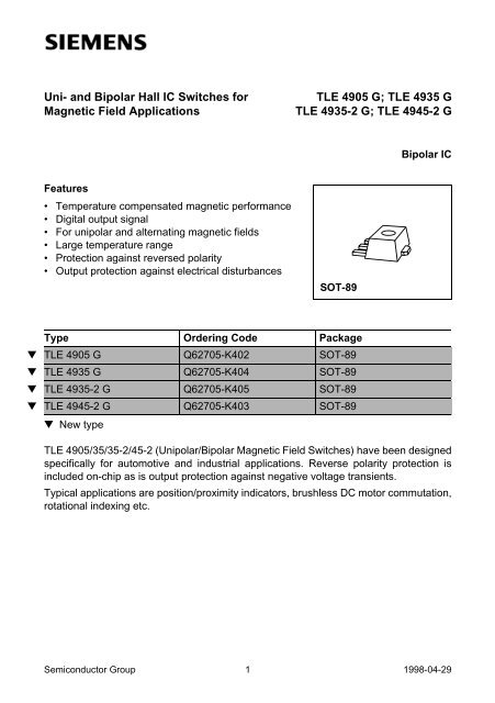
Uni- and Bipolar Hall IC Switches forMagnetic Field Applications<strong>TLE</strong> 4905 G; <strong>TLE</strong> <strong>4935</strong> G<strong>TLE</strong> <strong>4935</strong>-2 G; <strong>TLE</strong> 4945-2 GBipolar ICFeatures• Temperature compensated magnetic performance• Digital output signal• For unipolar and alternating magnetic fields• Large temperature range• Protection against reversed polarity• Output protection against electrical disturbancesSOT-89Type Ordering Code Package▼ <strong>TLE</strong> 4905 G Q62705-K402 SOT-89▼ <strong>TLE</strong> <strong>4935</strong> G Q62705-K404 SOT-89▼ <strong>TLE</strong> <strong>4935</strong>-2 G Q62705-K405 SOT-89▼ <strong>TLE</strong> 4945-2 G Q62705-K403 SOT-89▼ New type<strong>TLE</strong> 4905/35/35-2/45-2 (Unipolar/Bipolar Magnetic Field Switches) have been designedspecifically for automotive and industrial applications. Reverse polarity protection isincluded on-chip as is output protection against negative voltage transients.Typical applications are position/proximity indicators, brushless DC motor commutation,rotational indexing etc.Semiconductor Group 1 1998-04-29
<strong>TLE</strong> 4905 G; <strong>TLE</strong> <strong>4935</strong> G<strong>TLE</strong> <strong>4935</strong>-2 G; <strong>TLE</strong> 4945-2 GPin Configuration(top view)2.25 ±0.2Center ofsensitive area1±0.21 2 3AEP02150Figure 1Pin Definitions and FuntionsPin No. Symbol Function1 V SSupply voltage2 GND Ground3 Q OutputSemiconductor Group 2 1998-04-29
<strong>TLE</strong> 4905 G; <strong>TLE</strong> <strong>4935</strong> G<strong>TLE</strong> <strong>4935</strong>-2 G; <strong>TLE</strong> 4945-2 GCircuit DescriptionThe circuit includes Hall generator, amplifier and Schmitt-Trigger on one chip. Theinternal reference provides the supply voltage for the components. A magnetic fieldperpendicular to the chip surface induces a voltage at the hall probe. This voltage isamplified and switches a Schmitt-trigger with open-collector output. A protection diodeagainst reverse power supply is integrated.The output is protected against electrical disturbances.ThresholdGeneratorV S1Hall-Generator3QV SV RefOutputAmplifierSchmitt-Trigger2GNDStageAEB01243Figure 2Block DiagramSemiconductor Group 3 1998-04-29
<strong>TLE</strong> 4905 G; <strong>TLE</strong> <strong>4935</strong> G<strong>TLE</strong> <strong>4935</strong>-2 G; <strong>TLE</strong> 4945-2 GFunctional Description Unipolar Type <strong>TLE</strong> 4905 (figure 3 and 4)When a positive magnetic field is applied in the indicated direction (figure 3) and theturn-on magnetic induction B OPis exceeded, the output of the Hall-effect IC will conduct(Operate Point). When the magnetic field is reduced to a value smaller than the releasepoint, the output of the IC turns off (Release Point; figure 4).ΙSNBranded SideV Q++V S-AES01231Figure 3Sensor/Magnetic-Field ConfigurationBB OPB RPInduction0tV QV QHOutput VoltageV QLtAED01420Figure 4Switching Characteristics Unipolar TypeSemiconductor Group 4 1998-04-29
<strong>TLE</strong> 4905 G; <strong>TLE</strong> <strong>4935</strong> G<strong>TLE</strong> <strong>4935</strong>-2 G; <strong>TLE</strong> 4945-2 GFunctional Description Bipolar Type <strong>TLE</strong> <strong>4935</strong>/35-2/45-2 (figure 5 and 6)When a positive magnetic field is applied in the indicated direction (figure 5) and theturn-on magnetic induction B OPis exceeded, the output of the Hall-effect IC will conduct(Operate Point). The output state does not change unless a reverse magnetic fieldexceeding the turn-off magnetic induction |B RP| is exceeded. In this case the output willturn off (Release Point; figure 6).ΙSNBranded SideV Q++V S-AES01231Figure 5Sensor/Magnetic-Field ConfigurationBB OP0tInductionB RPV QV QHOutput VoltageV QLtAED01421Figure 6Switching Characteristics Bipolar TypeSemiconductor Group 5 1998-04-29
<strong>TLE</strong> 4905 G; <strong>TLE</strong> <strong>4935</strong> G<strong>TLE</strong> <strong>4935</strong>-2 G; <strong>TLE</strong> 4945-2 GAbsolute Maximum RatingsT j= – 40 to 125 °CParameter Symbol Limit Values Unit Remarksmin. max.Supply voltage V S – 40 32 V –Supply voltage V S – 40 V t < 400 ms; ν = 0.1Output voltage V Q – 32 V –Output current I Q – 100 mA –Output reverse current – I Q – 100 mA –Junction temperature T j – 40 125 °C –Storage temperature T stg – 50 150 °C –Thermal resistance R th JA 100 K/W –Note: Stresses above those listed here may cause permanent damage to the device.Exposure to absolute maximum rating conditions for extended periods may affectdevice reliability.Operating RangeParameter Symbol Limit Values Unit Remarksmin. max.Supply voltage V S4.0 18 V –Junction temperature T j– 40 125 °C –Note: In the operating range the functions given in the circuit description are fulfilled.Semiconductor Group 6 1998-04-29
<strong>TLE</strong> 4905 G; <strong>TLE</strong> <strong>4935</strong> G<strong>TLE</strong> <strong>4935</strong>-2 G; <strong>TLE</strong> 4945-2 GAC/DC Characteristics4.0 V ≤ V S≤ 18 V; – 40 °C ≤ T j≤ 125 °CParameter Symbol Limit Values Unit Test Condition Testmin. typ. max.CircuitSupply currentI SHigh–I SLow–2.53.578Note: The listed characteristics are ensured over the operating range of the integratedcircuit. Typical characteristics specify mean values expected over the productionspread. If not otherwise specified, typical characteristics apply at T j= 25 °C andthe given supply voltage.Note: Moderate changes may occur during the development process or customerdiscussion.mAmAB < B RPB > B OPI Q= 40 mAOutput saturation V QSat– 0.25 0.5 V I Q= 40 mA 1voltageOutput leakage I QL– – 10 µA V Q= 18 V 1currentRise/fall time t r/ t f– – 1 µs R L= 1.2 kΩC L≤ 33 pF111Semiconductor Group 7 1998-04-29
<strong>TLE</strong> 4905 G; <strong>TLE</strong> <strong>4935</strong> G<strong>TLE</strong> <strong>4935</strong>-2 G; <strong>TLE</strong> 4945-2 GMagnetic Characteristics4.0 V ≤ V S≤ 18 VParameter Symbol Limit Values Unit<strong>TLE</strong> 4905unipolar<strong>TLE</strong> <strong>4935</strong>bipolar latch<strong>TLE</strong> <strong>4935</strong>-2bipolar latch<strong>TLE</strong> 4945-2bipolarswitchmin. max. min. max. min. max. min. max.Junction Temperature T j= – 40 °CTurn-ONinductionTurn-OFFinductionHysteresis(B OP-B RP)7.5B OP∆B HY2B RP5.519176.510– 202020– 104015– 273027– 1554– 3– 61635mTmTmTJunction Temperature T j= 25 °CTurn-ONinductionTurn-OFFinductionHysteresis(B OP-B RP)7B OP∆B HY2B RP51816610– 202020– 104014– 262826– 1452– 3– 61635mTmTmTJunction Temperature T j= 85 °CTurn-ONinductionTurn-OFFinductionHysteresis(B OP-B RP)B OP6.5B RP4.5∆B HY217.5155.510– 202020– 104013– 262626– 1352– 3– 61635mTmTmTJunction Temperature T j= 125 °CTurn-ONinductionTurn-OFFinductionHysteresis(B OP-B RP)6B OP∆B HY2B RP41714510– 202020– 104012– 252425– 1250– 3– 61635mTmTmTNote: The listed characteristics are ensured over the operating range of the integrated circuit.Typical characteristics specify mean values expected over the production spread. If nototherwise specified, typical characteristics apply at T j= 25 °C and the given supply voltage.Semiconductor Group 8 1998-04-29
<strong>TLE</strong> 4905 G; <strong>TLE</strong> <strong>4935</strong> G<strong>TLE</strong> <strong>4935</strong>-2 G; <strong>TLE</strong> 4945-2 GΙ SΙQQV S+-4.7 nFR L312V SGND<strong>TLE</strong>4905/35/35-2/45-2C LAES01244Unipolar Type <strong>TLE</strong> 4905 Bipolar Type <strong>TLE</strong> <strong>4935</strong>VQVQV QHV QHV QL0B RPB OPBV QL0B RPB OPBB HYB HYAED01422VQV QH0.9 V QHV QH0.1t rt ftAED01246Figure 7 Test Circuit 1Semiconductor Group 9 1998-04-29
<strong>TLE</strong> 4905 G; <strong>TLE</strong> <strong>4935</strong> G<strong>TLE</strong> <strong>4935</strong>-2 G; <strong>TLE</strong> 4945-2 GMainframeLineSensorV S1V S4.7 nFSignal1.2 kΩ4.7 nF23GNDQ<strong>TLE</strong>4905/35/35-2/45-2AES01247Figure 8Application CircuitSemiconductor Group 10 1998-04-29
<strong>TLE</strong> 4905 G; <strong>TLE</strong> <strong>4935</strong> G<strong>TLE</strong> <strong>4935</strong>-2 G; <strong>TLE</strong> 4945-2 GIf not otherwise specified, all curves reflect typical values at T j= 25 °C and V S= 12 V.Quiescent Current DifferenceSaturation Voltage versusversus TemperatureOutput Current1.0AED014591.2AED01461mA0.75∆Ι= Ι - ΙSSLowΙ Q = 40 mASHighV1.04.0 V _
<strong>TLE</strong> 4905 G; <strong>TLE</strong> <strong>4935</strong> G<strong>TLE</strong> <strong>4935</strong>-2 G; <strong>TLE</strong> 4945-2 G<strong>TLE</strong> <strong>4935</strong> Operate-and Release-Pointversus Junction Temperature<strong>TLE</strong> <strong>4935</strong>-2 Operate-and Release-Pointversus Junction TemperatureB30mT204.0 V _
<strong>TLE</strong> 4905 G; <strong>TLE</strong> <strong>4935</strong> G<strong>TLE</strong> <strong>4935</strong>-2 G; <strong>TLE</strong> 4945-2 GPackage OutlineSOT-89 (SMD)(Plastic Small Outline Transistor Package)4.545˚+0.21.50.25 acc. to0.2 max1)DIN 67841.612.6 max4.25 max10˚ max2.75+0.1-0.151.50.65 max0.25 min1.0 ±0.231)Ejector pin marking possibleGPS05558Package Informationdd: Distance chip to upper side of ICSOT-89: 1.05 mmAEA02487Sorts of PackingPackage outlines for tubes, trays etc. are contained in ourData Book “Package Information”.SMD = Surface Mounted DeviceDimensions in mmSemiconductor Group 13 1998-04-29
This datasheet has been downloaded from:www.<strong>Datasheet</strong><strong>Catalog</strong>.com<strong>Datasheet</strong>s for electronic components.