AN804 P-Channel MOSFETs, the Best Choice for High ... - Vishay
AN804 P-Channel MOSFETs, the Best Choice for High ... - Vishay
AN804 P-Channel MOSFETs, the Best Choice for High ... - Vishay

You also want an ePaper? Increase the reach of your titles
YUMPU automatically turns print PDFs into web optimized ePapers that Google loves.
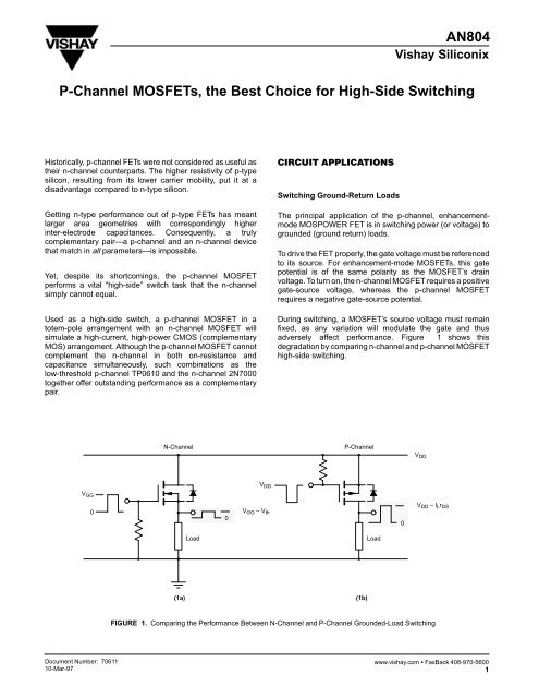
<strong>AN804</strong><strong>Vishay</strong> SiliconixP-<strong>Channel</strong> <strong>MOSFETs</strong>, <strong>the</strong> <strong>Best</strong> <strong>Choice</strong> <strong>for</strong> <strong>High</strong>-Side SwitchingHistorically, p-channel FETs were not considered as useful as<strong>the</strong>ir n-channel counterparts. The higher resistivity of p-typesilicon, resulting from its lower carrier mobility, put it at adisadvantage compared to n-type silicon.Getting n-type per<strong>for</strong>mance out of p-type FETs has meantlarger area geometries with correspondingly higherinter-electrode capacitances. Consequently, a trulycomplementary pair—a p-channel and an n-channel devicethat match in all parameters—is impossible.Yet, despite its shortcomings, <strong>the</strong> p-channel MOSFETper<strong>for</strong>ms a vital “high-side” switch task that <strong>the</strong> n-channelsimply cannot equal.Used as a high-side switch, a p-channel MOSFET in atotem-pole arrangement with an n-channel MOSFET willsimulate a high-current, high-power CMOS (complementaryMOS) arrangement. Although <strong>the</strong> p-channel MOSFET cannotcomplement <strong>the</strong> n-channel in both on-resistance andcapacitance simultaneously, such combinations as <strong>the</strong>low-threshold p-channel TP0610 and <strong>the</strong> n-channel 2N7000toge<strong>the</strong>r offer outstanding per<strong>for</strong>mance as a complementarypair. Switching Ground-Return LoadsThe principal application of <strong>the</strong> p-channel, enhancementmodeMOSPOWER FET is in switching power (or voltage) togrounded (ground return) loads.To drive <strong>the</strong> FET properly, <strong>the</strong> gate voltage must be referencedto its source. For enhancement-mode <strong>MOSFETs</strong>, this gatepotential is of <strong>the</strong> same polarity as <strong>the</strong> MOSFET’s drainvoltage. To turn on, <strong>the</strong> n-channel MOSFET requires a positivegate-source voltage, whereas <strong>the</strong> p-channel MOSFETrequires a negative gate-source potential.During switching, a MOSFET’s source voltage must remainfixed, as any variation will modulate <strong>the</strong> gate and thusadversely affect per<strong>for</strong>mance. Figure 1 shows thisdegradation by comparing n-channel and p-channel MOSFEThigh-side switching.N-<strong>Channel</strong>P-<strong>Channel</strong>V DDV DDV GG00V GG – V th0V DD – I L r DSLoadLoad(1a)(1b)FIGURE 1. Comparing <strong>the</strong> Per<strong>for</strong>mance Between N-<strong>Channel</strong> and P-<strong>Channel</strong> Grounded-Load SwitchingDocument Number: 7061110-Mar-97www.vishay.com FaxBack 408-970-56001
<strong>AN804</strong><strong>Vishay</strong> SiliconixIf an n-channel, enhancement-mode MOSFET were switchinga positive-polarity voltage to a grounded load, <strong>the</strong> output wouldbe limited to V GG – V th .The equations describing per<strong>for</strong>mance of <strong>the</strong> n-channelground-switching MOSFET with a ground-reference gate driveare based on <strong>the</strong> relationship between V DD and V GG :If V DD ≥ V GG , <strong>the</strong>n V O = V GG – V th ;If V DD < V GG – V th . <strong>the</strong>n V O = V DD – I L r DS(on) .Sustaining a more acceptable gain with an output in directrelation to V DD would require an isolated gate drive referencedto <strong>the</strong> source (Figure 4). The dc bias option rectifies <strong>the</strong> pulseof ac from <strong>the</strong> trans<strong>for</strong>mer and stores a “+” voltage on <strong>the</strong>gate-to-source capacitance of <strong>the</strong> MOSFET. The RCdetermines <strong>the</strong> turn off time.Bootstrapping <strong>the</strong> n-channel MOSFET (Figure 2) issatisfactory <strong>for</strong> short turn-on times of a few milliseconds. In thisarrangement, both <strong>MOSFETs</strong> must have breakdown voltagespecifications that match or exceed <strong>the</strong> supply voltage.Using a p-channel MOSFET may place some severerestraints on <strong>the</strong> gate drive, since <strong>the</strong> gate must be close toV DD (Figure 1b). To return gate control to a more acceptablelogic <strong>for</strong>mat, add an n-channel MOSFET (Figure 3).Using an n-channel MOSFET in this way simplifies <strong>the</strong> gatedrive <strong>for</strong> a high-voltage, high-side, p-channel MOSFET.Placing a Zener diode between <strong>the</strong> gate and supply ensuresthat V (BR)GSS will not be exceeded. Again, both <strong>MOSFETs</strong>must withstand <strong>the</strong> full rail voltage.ARCLoadBdc BiasOptionsFIGURE 4. Floating Gate DriveV DDV DD15 VP-<strong>Channel</strong>V DD – I L r DSN-<strong>Channel</strong>N-<strong>Channel</strong>TTLN-<strong>Channel</strong>TTLLoadFIGURE 2. Bootstrapping <strong>for</strong> N-<strong>Channel</strong>Grounded-Load SwitchingFIGURE 3. Using An N-<strong>Channel</strong> Level-ShifterSimplifies Driving From Logicwww.vishay.com FaxBack 408-970-56002Document Number: 7061110-Mar-97
<strong>AN804</strong><strong>Vishay</strong> SiliconixHalf-Bridge (Totem Pole)A high-side p-channel MOSFET and a low-side n-channelMOSFET tied with common drains (Figure 5) make a superbhigh-current “CMOS equivalent” switch. One fault common tosuch circuits has been <strong>the</strong> excessive crossover current duringswitching that may occur if <strong>the</strong> gate drive allows both<strong>MOSFETs</strong> to be on simultaneously.+V DD+15 VA resistively-coupled lower-power complementary pairoffers extremely low crossover current when <strong>the</strong> output stageuses high-power <strong>MOSFETs</strong>. The Zener, Z1, and resistors, R1and R3, act as a level shifter, properly driving <strong>the</strong> low-power<strong>MOSFETs</strong>. The Zener may be selected according to <strong>the</strong>equationV ZENER = 2 V DD – V th where +V DD = –V DD+15 V–15 VP-<strong>Channel</strong>N-<strong>Channel</strong>V OUTWhatever crossover current that might occur in <strong>the</strong> low-powerdrivers is dramatically reduced by <strong>the</strong> series resistor, R4.Additionally, driving <strong>the</strong> high-power complementary pair usingthis resistor divider scheme all but eliminates crossovercurrent in this critical output driver. This increases both <strong>the</strong>driver’s efficiency and its reliability.–V DD–15 V I DDFIGURE 5. Low-Voltage ComplementaryMOSPOWER ArrayProperly driving <strong>the</strong> MOSFET gates can minimize unwantedcrossover current at high supply voltages (both +V DD and –V DD )(Figure 6).PartNumber V (BR)DSS (V) r DS Max () I D (A)Si9939DY 30/–30 0.05/0.1 3.5/–3.5Si9942DY 20/–20 0.125/0.2 3/–2.5Si9928DY 20/–20 0.05/0.11 5/–3.4+V DDR1P-<strong>Channel</strong>R2Z1R4TTLN-<strong>Channel</strong>N-<strong>Channel</strong>R3–V DDFIGURE 6. <strong>High</strong>-Voltage Complementary Pair Driven by Logic-Compatible MOSFETDocument Number: 7061110-Mar-97www.vishay.com FaxBack 408-970-56003
<strong>AN804</strong><strong>Vishay</strong> Siliconix P-<strong>Channel</strong> DevicesN-<strong>Channel</strong> DevicesPart Number V (BR)DSS Min (V) r DS Max () Package Part Number V (BR)DSS Min (V) r DS Max () PackageVP0300L –30 2.5 TO-226AA VN0300L 30 1.2 TO-226AATP0610L –60 10 TO-226AA 2N7000 60 5 TO-226AAVP2020L –200 20 TO-226AA VN2010L 200 10 TO-226AATP0101T* –12 0.65 TO-236 TN0200T* 20 0.4 TO-236TP0610T* –60 10 TO-236 2N7002* 60 7.5 TO-236*Surface Mount Packagewww.vishay.com FaxBack 408-970-56004Document Number: 7061110-Mar-97