Tight-binding description of patterned graphene
Tight-binding description of patterned graphene
Tight-binding description of patterned graphene

You also want an ePaper? Increase the reach of your titles
YUMPU automatically turns print PDFs into web optimized ePapers that Google loves.
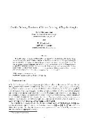
Semicond. Sci. Technol. 23 (2008) 075026B Gharekhanlou et alFigure 5. Typical patterning model <strong>of</strong> <strong>graphene</strong> with reduced symmetry (first- and second-nearest neighbors removed from the lattice).Hence, the atomic orbitals n (r), which are eigenfunctions<strong>of</strong> the single-atom Hamiltonian H at are assumed to be verysmall at distances exceeding the lattice constant. This is whatis normally meant by the tight-<strong>binding</strong> method. We furtherassume that any corrections to the atomic potential U(r),which are required to obtain the full Hamiltonian H <strong>of</strong> thesystem, are appreciable only when the atomic orbitals aresmall. The solution to the time-independent single-electronSchrödinger equation φ(r) is then assumed to be a linearcombination <strong>of</strong> atomic orbitalsφ(r) = ∑ b n n (r).n(4)This leads to a matrix equation for the coefficients b m andBloch energies ε(κ) <strong>of</strong> the formε(κ) = E m − β m + ∑ R≠0γ m (R) exp(iκ · R)b m + ∑ R≠0α m (R) exp(iκ · R) . (5)Here, E m is the energy <strong>of</strong> the mth atomic level, and∫β m =− m ∗ (r)U(r)φ(r) d3 r, (6a)α m (R) =∫m ∗ (r)φ(r − R) d3 r, (6b)∫γ m (R) =− m ∗ (r)U(r)φ(r − R) d3 r, (6c)are the corresponding transfer and overlap integrals.Before including the vacancy defects in <strong>graphene</strong>structure, we first calculate the band structure <strong>of</strong> <strong>graphene</strong>up to five nearest neighbors using the described tight-<strong>binding</strong>approach. Then we omit the terms related to the absentatoms from the summation <strong>of</strong> atomic potential terms in theHamiltonian. Here, as is normally done in the standard tight<strong>binding</strong>approximation, α m and β m are neglected in (5), andjust have applied the effect <strong>of</strong> the last overlap integral. Also,we note that in <strong>graphene</strong>, each <strong>of</strong> the two nearest atoms haveatomic orbital n (r) with opposite signs for the overall atomicorbitals as ±p z . The overlapping orbital obtained by theinterference <strong>of</strong> p z orbitals corresponds to the energy bandstructure ε(κ), and in particular π and π ∗ electronic bands asshowninfigure1.In figure 2, the arrangement <strong>of</strong> carbon atoms in <strong>graphene</strong>sheet is illustrated together its unit basis vectors, and the threenearest neighbors surrounding a central atom. As can be seenhere, there are three nearest, six second-nearest, three thirdnearestneighbors, etc. In figure 3 Dirac point is clearly seen(marked by the black circle) in the side view from the bandstructure <strong>of</strong> <strong>graphene</strong>. The calculations are done here by takingonly the first-nearest neighbors. As is evident from this figure,π and π ∗ electronic bands are almost completely conical acrossthe Dirac point. We also have calculated the band structure<strong>of</strong> <strong>graphene</strong> again this time with taking five nearest neighborsinto account. Since the computational cell size is artificiallyincreased, the band structure squeezes in the reciprocal space.Nevertheless, the symmetry and degeneracy at Dirac pointsare still preserved.In figure 4 the band structure <strong>of</strong> a <strong>patterned</strong> <strong>graphene</strong> isshown, with some atoms periodically taken out <strong>of</strong> the lattice.As can be easily seen, there is no further degeneracy at thepreviously Dirac points remains. In other words, an energygap is opened in justification <strong>of</strong> the diagram in figure 1. Asthe number <strong>of</strong> defects in a cell is increased, by taking thenext set <strong>of</strong> nearest neighbors, the corresponding energy gapvaries significantly as in table 1. Here, the energy gap reachesa maximum, when two <strong>of</strong> the second-nearest neighbors aredeleted. For instance, for the structure illustrated in figure 5,the symmetry point group is reduced from the original C 6 vpoint group to its C 3 v sub-group. The new super cellis marked with the dashed hexagon, which now includes1+3× 1+6× 1 2 +6× 1 = 9 atoms in each cell.3In contrast, Zhou et al [18] have recently obtained anenergy gap <strong>of</strong> 0.26 eV, a value close to that <strong>of</strong> our structure,by removing the translational symmetry. They have achievedthis symmetry breaking through lattice-mismatched expitaxialgrowth <strong>of</strong> <strong>graphene</strong> on SiC, which results in a strained<strong>graphene</strong> lattice. Finally, the dependence <strong>of</strong> the Fermioneffective mass on the number <strong>of</strong> defects is also tabulated intable 1 along the principal orthogonal directions. There is a4