
You also want an ePaper? Increase the reach of your titles
YUMPU automatically turns print PDFs into web optimized ePapers that Google loves.
’<br />
*<br />
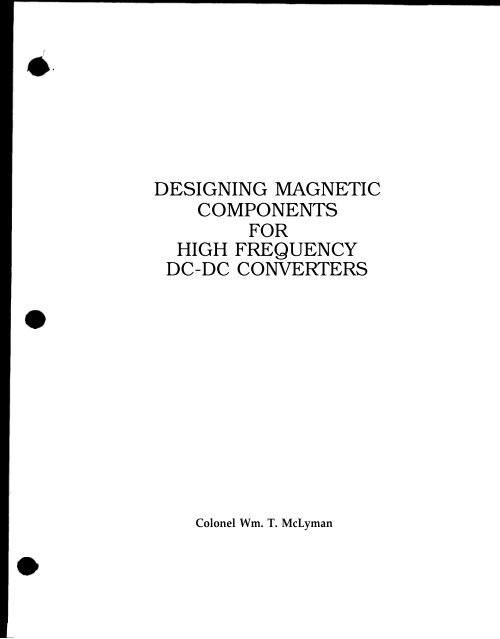
DESIGNING MAGNETIC<br />
COMPONENTS<br />
FOR<br />
HIGH FREQUENCY<br />
DC-DC CONVERTERS<br />
Colonel Wm. T. McLyman
a<br />
@<br />
DESIGNING MAGNETIC<br />
COMPONENTS<br />
FOR<br />
HIGH FREQUENCY<br />
DC-DC CONVERTERS<br />
ii
Other Books and Software by the Author<br />
BQQks<br />
Mo~netic Core Selection for Trnnsfortners mui lnchctors<br />
Marcel Dekker, 270 Madison Ave., New York, NY 10016<br />
Transformer and huluctor Design Hflndbook (second edition)<br />
Marcel Dekker, 270 Madison Ave., New York, NY 10016<br />
S..dmme<br />
Computer Aided Design for inductors nnd Trmsfornws<br />
Kg Magnetics Inc. 2135 Huntington Drive Suite 201D, San Marirm, Ca. 91108<br />
Flybmk Converter Magnetics Design<br />
Kg Magnetics Inc. 2135 Huntington Drive Suite 201 D, San Marine,Ca.91108<br />
MnSnr’tic Core Conversion<br />
Kg Magnetics Inc. 2135 Huntington Drive Suite 201D, San Marirm,Ca.91108<br />
Specialty 1 Design Mognetics<br />
Kg Magnetics inc. 2135 Huntington Drive Suite 2011J, San Marine,Ca.91108<br />
Spccinlty 11 Design Mr?gtwtics<br />
Kg Magnetics Inc. 2135 Huntington Drive Suite 201 D, San Marine,Ca.91108<br />
Cowpufer Aided ?W@ormer and lwfuctor Analysis<br />
Kg Magnetics Inc. 2135 Huntington Drive Suite 2011>, San Marine,Ca.91108<br />
I’here are also 17 leading manufacturers core data disks available.<br />
When you buy the above software it will never becomes obsolete. The software is updated at<br />
least once a year. The only Charge is for postage and handling.<br />
Kg Magnetics Inc.<br />
2135 Huntington Drive<br />
Suite 201D, San Marine, Ca. 91108<br />
Phone (818) 568-8443<br />
FAX (818) 568-8534<br />
Metglas~M is a registered trademark of Allied-Signal, Inc.<br />
Kool Mpl M<br />
is a registered trademark of Magnetics, L>ivisicm of Spang & Co.<br />
. . .<br />
111
Library of Congress Cataloging in Publication Data<br />
Mcl ,yman Colonel William T.<br />
Designing Magnetic Components for High Frequency DC-DC Converters<br />
Bibliography : p.<br />
lr-wludes index.<br />
1. Electronic transformers.<br />
Copyright @ 1993 by Kg Magnetics, Inc. All Rights Reserved<br />
The design equations and format used in the examples presented in this book were taken from<br />
the author’s design software programs. The titles of the software prograrm are mentioned earlier<br />
in this book, The design equations and design procedures are to be used by the individual<br />
engineer for design and evaluation of magnetic components. The design equations and/or<br />
design procedures illustrated in this book cannot be developed into software that can be<br />
disseminated in any form that would be in direct or indirect competition with the author’s<br />
software. Neither this book nor any part may be reproduced or transmitted in any form or by<br />
any means, electronic or mechanical, including photocopying, microfilming, and recording, or by<br />
any information storage and retrieval system, without permission in writing from the publisher.<br />
Kg Magnetics, Inc.<br />
2135 Huntington Drive<br />
Suite 201D<br />
San Marine, Ca. 91108<br />
Phone (818) 568-8443<br />
FAX (818) 568-8534<br />
Current printing (last digit)<br />
10987654321<br />
I’RINTED IN THE UNITED STATES (’)F AMERICA<br />
iv
Disclaimer<br />
All statements, information, and data given herein are believed<br />
to be accurate and reliable, but are presented without guarantee,<br />
warranty, or responsibility of any kind, expressed or implied.<br />
Statements or suggestions concerning possible use of this book,<br />
including but not limited to the design of magnetic components,<br />
are made without representation or warranty that any such use<br />
is free of patent infringement, and are not recommendations to<br />
infringe any patents. The user should not assume that all safety<br />
measures are indicated, or that other measures may not be<br />
required.
m<br />
lf a “history of the evolution of United States education in the fields of power electronics is written<br />
at some point in time in the future, it will most certainly discuss the lack of educational courses<br />
in practical magnetics design that has continued since the end of World War 11.<br />
Even today, where magnetics design is often considered by many institutions of higher learning<br />
as an “outdated and outmoded” subject, this educational problem continues to flourish. Yet,<br />
every modern electronic product today requires some form of power-processing or power-<br />
conditioning circuit for proper operation, and those circuits enviably contain magnetic<br />
components.<br />
Over the past fourteen years, Colonel McLyman’s best-selling two books on magnetic design<br />
principles have provided working engineers with easy-to-use analytical tools to develop<br />
practical and reliable magnetic components of all varieties. These books have, for many of us,<br />
filled the educational void that our college engineering experiences left unfilled, and are now<br />
considered essential reading for new engineers entering the fields of power electronics design,<br />
[&fA t+~ ~
Preface<br />
This book has been written primarily to assist the circuit design engineer with the design of<br />
power magnetics for different topologies used in dc to dc converters.<br />
There are now available new integrated circuit pulse-width-modulating chips (1’WM) that<br />
simplify the dc to dc converter design. These new PWM chips and the ease of their use have<br />
opened up many power circuit topologies from which the design engineer choose. Each circuit<br />
topology has its good and bad features. These features range from parts count, parts stress<br />
stability, and complexity, There is a tendency for the design engineers to stay with an<br />
established design with which they are more familiar even though the design may not be<br />
optimum for the application. This is done because of good results from past designs and a good<br />
handle cm the design procedure for the power magnetic components.<br />
The conversion process in power electronics requires the use of magnetic components which are<br />
often the heaviest and bulkiest items in the power conversion circuit. They also have a significant<br />
effect on the system’s overall performance and efficiency. Accordingly, the design of such<br />
components has an important influence on overall system weight, power conversion efficiency,<br />
and cost. Because of the interdependence and interaction of parameters, judicious tradeoffs are<br />
necessary to achieve design optimization.<br />
Traditionally, the design of magnetic components for power conversion circuits has been very<br />
time-consuming even for a single component, and extremely burdensome when multiple<br />
components are involved. The result, in many instances, is a component in which the design is<br />
not optimized.<br />
The main goal of this book is to enlighten the engineer by a step-by-step design procedure for<br />
different types of power circuit topologies, The design engineer will be able to see various circuit<br />
topologies to compare performance, He/she will be able to see how the magnetics are designed<br />
to a given specification, from picking the core to selecting the correct wire size to meet the<br />
regulation and temperature rise. From these design examples the engineer can now assess the<br />
complexity of the design and make tradeoffs as to which is better suited for the application.
e The material is organized so the student engineer or technician, starting at the beginning of the<br />
book and continuing through to the end, will gain a comprehensive knowledge in transformer<br />
and inductor design for different topologies used in dc to dc converters.<br />
No responsibility is assumed by the author or the publisher for any infringement of patent or<br />
other rights of third parties which may result from the use of circuits, systems, or processes<br />
described or referred to in this book.<br />
1 wish to thank the manufacturers represented in this book for their assistance in supplying<br />
technical data.<br />
Colonel Wm. T. McLyrnan<br />
. . .<br />
VIII
Acknowledgments<br />
In gathering the material for this book, the author has been fortunate in having the assistance and<br />
cooperation of several companies, and many people, The author wishes to express his gratitude<br />
to all of.them. I’he list is too long to mention them all, However, there are some individuals and<br />
companies whose contributions have been significant, Colleagues at Magnetics include Robert<br />
Noah and Charles Eaves who supplied cores, test data, catalogs and Harry Savisky who helped<br />
so much with the editing of the final draft. My colleagues at Micrc)metals, Jim Cox and Walt<br />
I.ewis, supplied cores, test data and catalogs. 1 would like to thank Joseph Elias of Allied Signal<br />
inc., Metglas Products, for supplying cores, test data and catalogs. 1 would also like to thank Ron<br />
Vinsant of Linear Technology, for supplying I.C’s and catalogs.<br />
I’here are some individuals 1 would also like to thank, Gordon Bloom and Jerry Fridenberg who<br />
provided their areas of expertise and valuable suggestions, and a long time friend of over 35<br />
years, Charles (CT) Kleiner for his editing and his drive for clarity. I am also indebted to Kit Sum<br />
for his assistance in the detailed derivations of many of the formulas and his efforts in checking<br />
the methodologies used; also Robert Yahiro for his persistence in detail and consistency<br />
regarding the design examples. There are people here at JPL 1 want to thank: Robert Detwiler,<br />
my group supervisor, for his encouragement; Dr. Vatch6 Vorperian for his help in generating and<br />
clarifying some equations; and Michael Hasbach for building and testing all of the magnetic<br />
components used in the design examples.<br />
ix
Symbols<br />
c1<br />
Ac<br />
‘P<br />
At<br />
Aw<br />
‘w(B)<br />
Aw(l)<br />
AWp<br />
A Ws<br />
Awtp<br />
Awts<br />
D<br />
1) max<br />
D min<br />
Dw<br />
E’<br />
Eng<br />
1]<br />
f<br />
‘r<br />
H<br />
1<br />
IC<br />
Regulation, Y.<br />
effective cross section of the core, cm2<br />
area product, cm 4<br />
surface area of the transformer, cm 2<br />
wire area, cn12<br />
bare wire area, cn~2<br />
insulated wire area, cm 2<br />
primary wire area, cm 2<br />
secondary wire area, cm 2<br />
total primary wire area, cm 2<br />
total secondary wire area, cn~2<br />
American Wire Gage<br />
alternating current flux density, tesla<br />
change in flux, tesla<br />
direct current flux density, tesla<br />
flux density, tesla<br />
residual flux density, tesla<br />
saturation flux density, tesla<br />
duty ratio<br />
maximum duty ratio<br />
minimum duty ratio<br />
dwell duty ratio<br />
voltage<br />
energy, watt-second<br />
efficiency<br />
frequency, Hz<br />
winding length, cm<br />
skin depth, cm<br />
magnetizing force, oersteds<br />
current, amps<br />
charge current, amps
Symbols (cont.)<br />
Al<br />
]d<br />
1.In<br />
IL<br />
I m<br />
1 0<br />
lo(max)<br />
‘o(min)<br />
‘P<br />
]Pk<br />
1 rms<br />
IS<br />
J<br />
Ke<br />
Kf<br />
‘~<br />
KL1<br />
L<br />
L(rnin)<br />
L,(nlax)<br />
A<br />
A<br />
‘II<br />
1 m<br />
MLT<br />
MPL<br />
pl<br />
Pm<br />
pr<br />
delta current, amps<br />
diode current, amps<br />
input current, amps<br />
inductor current, amps<br />
magnetizing current, amps<br />
load current, amps<br />
maximum load current, amps<br />
minimum load current, amps<br />
primary current, amps<br />
peak current, amps<br />
mot mean square current, amps<br />
secondary current, amps<br />
current density, amps per cm 2<br />
electrical coefficient<br />
wave form coefficient<br />
core geometry coefficient<br />
window utilization factor<br />
inductance, henry<br />
minimum inductance, henry<br />
maximum inductance, henry<br />
volt-seconds<br />
watt density, cm 2<br />
gap, cm<br />
magnetic path, cm<br />
mean length turn, cm<br />
magnetic path length, cm<br />
initial permeability<br />
incremental permeability<br />
core material permeability<br />
relative permeability<br />
xi
Symbols (cont.)<br />
I-1<br />
o~<br />
P<br />
r’ Cu<br />
Pfe<br />
P“ m<br />
I’~b<br />
I’.<br />
‘P<br />
1’s<br />
r’~<br />
r’~<br />
I’t”<br />
rtp<br />
rts<br />
R<br />
I< cu<br />
R ma x<br />
R min<br />
1
Symbols (cont.)<br />
S1<br />
S’2<br />
SCJ<br />
S4<br />
T<br />
‘on<br />
toff<br />
tpw<br />
I’r<br />
ts<br />
tw<br />
ttw<br />
VA<br />
v~<br />
vd<br />
v“ m<br />
vm~~<br />
Vmi *<br />
V.<br />
‘P<br />
vQ<br />
Vs<br />
w<br />
Wa<br />
w-s<br />
Wtcll<br />
Wtfe<br />
conductor area/wire area<br />
wound area /usable window<br />
usable window area /window area<br />
usable window area/usable window area + insulation area<br />
total period, seconds<br />
transistor on time, seconds<br />
transistor off time, seconds<br />
pulse width, seconds<br />
temperature rise, degrees C<br />
time to saturate the mag-amp<br />
dwell time, seconds<br />
total dwell time, seconds<br />
volt-amps<br />
control voltage, volts<br />
diode voltage drop, volts<br />
input voltage, volts<br />
maximum applied voltage<br />
minimum applied voltage<br />
output voltage, volts<br />
primary voltage, volts<br />
voltage across device when on, volts<br />
secondary voltage, volts<br />
watts<br />
window area, cm 2<br />
watt-seconds<br />
copper weight, grams<br />
iron weight, grams<br />
. . .<br />
XIII
Contents<br />
Forward . . . . . . . . . . . . . . . . . . . . . . . . . . . . . . . . . . . . . . . . . . . . . . . . . . . . . . . . . . vi<br />
l’reface . . . . . . . . . . . . . . . . . . . . . . . . . . . . . . . . . . . . . . . . . . . . . . . . . . . . . . . . . . . vii<br />
Acknowledgment . . . . . . . . . . . . . . . . . . . . . . . . . . . . . . . . . . . . . . . . . . . . . . . . . . ix<br />
Symbols . . . . . . . . . . . . . . . . . . . . . . . . . . . . . . . . . . . . . . . . . . . . . . . . . . . . . . . . . . x<br />
Chapter I<br />
introduction . . . . . . . . . . . . . . . . . . . . . . . . . . . . . . . . . . . . . . . . . . . . . . . . . . . . . . 2<br />
Magnetic Coreand itsPowerHandling Capability . . . . . . . . . . . . . . . . . . . . . . . . . . . 2<br />
Core Geonletry . . . . . . . . . . . . . . . . . . . . . . . . . . . . . . . . . . . . . . . . . . . . . . . . . . . . . 3<br />
Transformers . . . . . . . . . . . . . . . . . . . . . . . . . . . . . . . . . . . . . . . . . . . . . . . . . 3<br />
Inductors . . . . . . . . . . . . . . . . . . . . . . . . . . . . . . . . . . . . . . . . . . . . . . . . . . . . . 4<br />
Transforn~erCcmsiderations. . . . . . . . . . . . . . . . . . . . . . . . . . . . . . . . . . . . . . . . . ...5<br />
Apparent I’ower . . . . . . . . . . . . . . . . . . . . . . . . . . . . . . . . . . . . . . . . . . . . . ...5<br />
Transformer withI’WM . . . . . . . . . . . . . . . . . . . . . . . . . . . . . . . . . . . . . . . . ...6<br />
Inductor Considerations . . . . . . . . . . . . . . . . . . . . . . . . . . . . . . . . . . . . . . . . . . . . . . 8<br />
Inductor Related Factors . . . . . . . . . . . . . . . . . . . . . . . . . . . . . . . . . . . . . . . . . 9<br />
PowderCore Considerations . . . . . . . . . . . . . . . . . . . . . . . . . . . . . . . . . . . . . . 11<br />
Window Utilization Factor.. . . . . . . . . . . . . . . . . . . . . . . . . . . . . . . . . . . . . . . . . . . 14<br />
Regulation andCopperLoss. . . . . . . . . . . . . . . . . . . . . . . . . . . . . . . . . . . . . . . . . . . 16<br />
TransformerEfficiencyand Regulation . . . . . . . . . . . . . . . . . . . . . . . . . . . . . . . . . . . . 18<br />
I’ulse Width Modulators(PWM) Integrated Circuit . . . . . . . . . . . . . . . . . . . . . . . . . . 19<br />
Voltage ModeControl . . . . . . . . . . . . . . . . . . . . . . . . . . . . . . . . . . . . . . . . . ...19<br />
Current Mode Control....;.. . . . . . . . . . . . . . . . . . . . . . . . . . . . . . . . . . . . . 20<br />
References . . . . . . . . . . . . . . . . . . . . . . . . . . . . . . . . . . . . . . . . . . . . . . . . . . . . . . ...22<br />
Chapter2 Magnetics In Switching Circuits<br />
]’ower Transformers in Switching Circuits<br />
introduction . . . . . . . . . . . . . . . . . . . . . . . . . . . . . . . . . . . . . . . . . . . . . . . . . . . 24<br />
I’ush-I’ull Switching Converter . . . . . . . . . . . . . . . . . . . . . . . . . . . . . . . . . . . . . 24<br />
IlalfBridgeSwitching Converter. . . . . . . . . . . . . . . . . . . . . . . . . . . . . . . . . . . . 26<br />
Full or HBridgeSwitchingConverter . . . . . . . . . . . . . . . . . . . . . . . . . . . . . . . . 28<br />
Single Ended Forward Switching Converter . . . . . . . . . . . . . . . . . . . . . . . . . . . 31<br />
Two Transistor Forward Switching Converter . . . . . . . . . . . . . . . . . . . . . . . . . . 33<br />
xiv
Contents (cont.)<br />
Current Fed Weinberg Switching Converter. . . . . . . . . . . . . . . . . . . . . . . . . . . . 34<br />
Mag-Amps for Switching Converters. . . . . . . . . . . . . . . . . . . . . . . . . . . . . . . . . 35<br />
Single Forward Mag-An~p Switching Converter. . . . . . . . . . . . . . . . . . . . . . . . . 37<br />
I’ush-Pull Mag-Amp Switching Converter. . . . . . . . . . . . . . . . . . . . . . . . .<br />
Energy Storage Inductors in Switching Circuits<br />
Introduction . . . . . . . . . . . . . . . . . . . . . . . . . . . . . . . . . . . . . . . . . . . . . . . . . .<br />
Energy Transfer . . . . . . . . . . . . . . . . . . . . . . . . . . . . . . . . . . . . . . . . . . . . . . .<br />
The Continuous and Discontinuous Boundary . . . . . . . . . . . . . . . . . . . . . . . . .<br />
Buck F1yback Regulator . . . . . . . . . . . . . . . . . . . . . . . . . . . . . . . . . . . . . . . . . .<br />
tkmstFlyb ackRegu labor . . . . . . . . ; . . . . . . . . . . . . . . . . . . . . . . . . . . . . . . . . .<br />
I]uck-Boost Inverting F1yback Regulator . . . . . . . . . . . . . . . . . . . . . . . . . . . . . .<br />
Iscdated Buck-Boost Flyback Regulator. . . . . . . . . . . . . . . . . . . . . . . . . . . . . . .<br />
Coupled C)utput Filter Inductor . . . . . . . . . . . . . . . . . . . . . . . . . . . . . . . . . . . .<br />
Input Filter Inductor . . . . . . . . . . . . . . . . . . . . . . . . . . . . . . . . . . . . . . . . . . . .<br />
C)utput Filter Inductor . . . . . . . . . . . . . . . . . . . . . . . . . . . . . . . . . . . . . . . . . . .<br />
References . . . . . . . . . . . . . . . . . . . . . . . . . . . . . . . . . . . . . . . . . . . . . . . . . . . .<br />
Cl~apter3 Power Magnetics Design Examples<br />
Introduction . . . . . . . . . . . . . . . . . . . . . . . . . . . . . . . . . . . . . . . . . . . . . . . . . . .<br />
Engineering Design Notes.... . . . . . . . . . . . . . . . . . . . . . . . . . . . . . . . . . . . . .<br />
Push-l’ull Ccmverter Design using anRMFerriteCore . . . . . . . . . . . . . . . . . . . .<br />
HalfBridgeConverter Designusing aPQFerriteCore . . . . . . . . . . . . . . . . . . . .<br />
Full Bridge Ccmverter Designusing aI’QFerriteCore . . . . . . . . . . . . . . . . . . . .<br />
Single Ended Forward Converter Design usingan ETDFerriteCore . . . . . . . . . .<br />
Two Transistor Forward Converter Design using an ETDFerriteCore . . . . . . . . .<br />
Weinberg Converter TransformerDesign usinganEFD-30 FerriteCore. . . . . . . .<br />
WeinbergConverter Input Inductor Design usinganMPI’powder Core . . . . . . .<br />
Single Ended Forward Short Circuit Mag-An~p Design using Perm 80 . . . . . . . . .<br />
Single Ended Forward Reg. Only Mag-An~p Design using Metglas 2714A . . . . . .<br />
Push-Pull Converter with Reg. only Mag-An~p Design using Metglas 2714A . . . .<br />
Input Inductor Design using an Iron I’owder Core . . . . . . . . . . . . . . . . . . . . . . .<br />
xv<br />
38<br />
40<br />
40<br />
41<br />
42<br />
43<br />
44<br />
46<br />
47<br />
49<br />
50<br />
52<br />
54<br />
55<br />
63<br />
75<br />
87<br />
99<br />
111<br />
121<br />
131<br />
141<br />
149<br />
157<br />
165
Contents (cont.)<br />
Buck Converter Design using a Met@as 2605TCA Gapped Core. . . . . . . . . . . . . 171<br />
Boost Converter Design Dis-Current using an EPC Ferrite Core . . . . . . . . . . . . 179<br />
Inverted B/B Conv. Design Dis-Current using an MIT’ Powder Core. . . . . . . . . 189<br />
Buck-Boost Isolated Design Dis-Current using an MM’ Powder Core . . . . . . . . . 199<br />
Boost Converter Design Con-Current using a PQ Ferrite Core. . . . . . . . . . . . . . . 213<br />
Inverted B/B Conv. Design Cont. Current using a Kool Mp Powder Core. . . . . . 221<br />
Buck-Boost Isolated Design Cont. Current using an MIT Powder Core. . . . . . . . 231<br />
Coupled Inductor Design using an MIT’ I’owder Core . . . . . . . . . . . . . . . . . . . . 245<br />
Single Ended Forward Output Filter Design using a High Flux Powder Core. . . . 255<br />
Push-Pull Output Filter Design using a Hign Flux Powder Core. . . . . . . . . . . . . . 2&3<br />
Low Power Drive Transformer using a Ferrite Toroidal Core. . . . . . . . . . . . . . . . 271<br />
References . . . . . . . . . . . . . . . . . . . . . . . . . . . . . . . . . . . . . . . . . . . . . . . . . . . . . . . . . 282<br />
Chapter 4 Soft Ferrites Cores<br />
introduction to Soft Ferrite Cores.. . . . . . . . . . . . . . . . . . . . . . . . . . . . . . . . . . . . . . .<br />
Ferrite Material Cross Reference.. . . . . . . . . . . . . . . . . . . . . . . . . . . . . . . . . . . . . . .<br />
Ferrite Core Manufacturers . . . . . . . . . . . . . . . . . . . . . . . . . . . . . . . . . . . . . . . . . . .<br />
information about Core Data Tables . . . . . . . . . . . . . . . . . . . . . . . . . . . . . . . . . . . . .<br />
1. Ferrite Core Data Tables<br />
RM Core Data . . . . . . . . . . . . . . . . . . . . . . . . . . . . . . . . . . . . . . . . .<br />
I’QCore Data . . . . . . . . . . . . . . . . . . . . . . . . . . . . . . . . . . . . . . . . . .<br />
RSCoreDat a . . . . . . . . . . . . . . . . . . . . . . . . . . . . . . . . . . . . . . . . .<br />
DSCore Data . . . . . . . . . . . . . . . . . . . . . . . . . . . . . . . . . . . . . . . . . .<br />
EPCore Data . . . . . . . . . . . . . . . . . . . . . . . . . . . . . . . . . . . . . . . . . .<br />
EC Core Data . . . . . . . . . . . . . . . . . . . . . . . . . . . . . . . . . . . . . . . . . .<br />
ETDCore Data . . . . . . . . . . . . . . . . . . . . . . . . . . . . . . . . . . . . . . . . .<br />
El’ CCoreDat a . . . . . . . . . . . . . . . . . . . . . . . . . . . . . . . . . . . . . . . .<br />
I’CCore Data . . . . . . . . . . . . . . . . . . . . . . . . . . . . . . . . . . . . . . . . . .<br />
EFDCore Data . . . . . . . . . . . . . . . . . . . . . . . . . . . . . . . . . . . . . . . . .<br />
EE&EILam Size Core Data..... . . . . . . . . . . . . . . . . . . . . . . . . . .<br />
EE&EICore Data . . . . . . . . . . . . . . . . . . . . . . . . . . . . . . . . . . . . . .<br />
Toroidal Core Data . . . . . . . . . . . . . . . . . . . . . . . . . . . . . . . . . . . . . .<br />
EE&EIPlanar Core I)ata . . . . . . . . . . . . . . . . . . . . . . . . . . . . . . . . .<br />
xvi<br />
284<br />
285<br />
286<br />
288<br />
289<br />
290<br />
291<br />
292<br />
293<br />
294<br />
295<br />
296<br />
297<br />
298<br />
299<br />
3(KI<br />
302<br />
304
Contents (cont.)<br />
2. Ferrite Core Loss Curves<br />
Ferrite Material Type P2500p . . . . . . . . . . . . . . . . . . . . . . . . . . . . . .<br />
Ferrite Material Type F3000p . . . . . . . . . . . . . . . . . . . . . . . . . . . . . .<br />
Ferrite Material Type R2300p . . . . . . . . . . . . . . . . . . . . . . . . . . . . . .<br />
Ferrite Material Type K1500~ . . . . . . . . . . . . . . . . . . . . . . . . . . . . . .<br />
Ferrite Material Type WIOOOOp . . . . . . . . . . . . . . . . . . . . . . . . . . . . .<br />
3. Ferrite Material Characteristics . . . . . . . . . . . . . . . . . . . . . . . . . . . . . . . . .<br />
FMaterial B-H Loop . . . . . . . . . . . . . . . . . . . . . . . . . . . . . . . . . . . . .<br />
KMaterial B-}l Loop . . . . . . . . . . . . . . . . . . . . . . . . . . . . . . . . . . . . .<br />
I’&RMaterial B-H Loop . . . . . . . . . . . . . . . . . . . . . . . . . . . . . . . . .<br />
WMaterial B-H Loop . . . . . . . . . . . . . . . . . . . . . . . . . . . . . . . . . . . .<br />
References . . . . . . . . . . . . . . . . . . . . . . . . . . . . . . . . . . . . . . . . . . . . . . . . . . . . . . . . .<br />
Chapter5 Iron Powder Cores<br />
Introduction to IronI’owderCores. . . . . . . . . . . . . . . . . . . . . . . . . . . . . . . . . . . . . . . 316<br />
iron Powder Core Manufacturers . . . . . . . . . . . . . . . . . . . . . . . . . . . . . . . . . . . . . . . . 317<br />
information about CoreDataTables . . . . . . . . . . . . . . . . . . . . . . . . . . . . . . . . . . . . . . 318<br />
l. Ircm I’owcter CoreDataTables. . . . . . . . . . . . . . . . . . . . . . . . . . . . . . . . . . 319<br />
2. Iron PowderC oreLossCurves<br />
Micrornetals 75p MaterialType-26. . . . . . . . . . . . . . . . . . . . . . . . . . . 325<br />
Micrometals35p MaterialType-08 . . . . . . . . . . . . . . . . . . . . . . . . . . . 326<br />
Micrometals 55p MaterialType-18 . . . . . . . . . . . . . . . . . . . . . . . . . . . 327<br />
Micrometals75p MaterialType-52 . . . . . . . . . . . . . . . . . . . . . . . . . . . 328<br />
3. iron Powder versusDCBias . . . . . . . . . . . . . . . . . . . . . . . . . . . . . . . . . ...329<br />
4. Iron Powder Material Characteriscis Table . . . . . . . . . . . . . . . . . . . . . . . . . 330<br />
5. Iron Powder Cores B- HLoops.<br />
Micrometals35~ MaterialType-08 . . . . . . . . . . . . . . . . . . . . . . . . . . . 331<br />
Micrometals55p MaterialType-18. . . . . . . . . . . . . . . . . . . . . . . . . . . 331<br />
Micrometals 75y MaterialType-26. . . . . . . . . . . . . . . . . . . . . . . . . . . 332<br />
Micrometals 75p MaterialType-52 . . . . . . . . . . . . . . . . . . . . . . . . . . . 332<br />
References . . . . . . . . . . . . . . . . . . . . . . . . . . . . . . . . . . . . . . . . . . . . . . . . . . . . . . ...333<br />
xvii<br />
305<br />
336<br />
307<br />
308<br />
309<br />
310<br />
311<br />
311<br />
312<br />
312<br />
313
Chapter 6 Nickel-Iron Powder Cores<br />
introduction to Nickel-Iron Powder Cores. . . . . . . . . . . . . . . . . . . . . . . . . . . . . . . . . 336<br />
Nickel-Iron Powder Core Manufacturers. . . . . . . . . . . . . . . . . . . . . . . . . . . . . . . . . . 337<br />
lnformaticm about Core Data Tables. . . . . . . . . . . . . . . . . . . . . . . . . . . . . . . . . . . . .. ’338<br />
l. MPI’Powder Core Data Tables. . . . . . . . . . . . . . . . . . . . . . . . . . . . . . . . . 339<br />
2, MPP Powder Core Loss Curves<br />
Magnetics M1’P125p . . . . . . . . . . . . . . . . . . . . . . . . . . . . . . . . . . . . . 343<br />
Magnetics MPP60p . . . . . . . . . . . . . . . . . . . . . . . . . . . . . . . . . . . . . . 344<br />
Magnetics MPP26p . . . . . . . . . . . . . . . . . . . . . . . . . . . . . . . . . . . . . . 345<br />
3. MPPPermeability versus Dc Bias. . . . . . . . . . . . . . . . . . . . . . . . . . . . . . . 346<br />
4. High Flux Powder Core Data Tables. . . . . . . . . . . . . . . . . . . . . . . . . . . . . 347<br />
5. High Flux Powder Core Loss Curves<br />
Magnetics High Flux 125p . . . . . . . . . . . . . . . . . . . . . . . . . . . . . . . . . 351<br />
Magnetics High F1ux60p . . . . . . . . . . . . . . . . . . . . . . . . . . . . . . . . . . 352<br />
Magnetics High Flux26p . . . . . . . . . . . . . . . . . . . . . . . . . . . . . . . . . . 353<br />
6. High Flux I’ermeability versus DC Bias . . . . . . . . . . . . . . . . . . . . . . . . . . . 354<br />
7. Kool MpPowder Core Data Tables . . . . . . . . . . . . . . . . . . . . . . . . . . . . . . 355<br />
8. Kool MpPowder Core Loss C~lrves<br />
Magnetics Kcml Mp125p/60p . . . . . . . . . . . . . . . . . . . . . . . . . . . . ...359<br />
9. Kool MpPern}eability versus Dc Bias . . . . . . . . ..e . . ..e . . . . ..o . . . . . . 360<br />
10. Nickel-Iron and KOO1 Mp Powder Core Material Characteristics. . . . . . . . . 361<br />
Molypermalloy B-H Loop . . . . . . . . . . . . . . . . . . . . . . . . . . . . . . . . . 362<br />
High Flux B-H Loop . . . . . . . . . . . . . . . . . . . . . . . . . . . . . . . . . . . . . 362<br />
Kool MpB-H Loop . . . . . . . . . . . . . . . . . . . . . . . . . . . . . . . . . . . . . . 3&?<br />
References . . . . . . . . . . . . . . . . . . . . . . . . . . . . . . . . . . . . . . . . . . .....e.q..e...,~~<br />
Chapter7 Nickel-Iron Tape Cores<br />
introduction to Nickel-Iron Tape Cores. . . . . . . . . . . . . . . . . . . . . . . . . . . . . . . . . . . . 366<br />
Nickel-Iron Tape Core Manufactllrers. . . . . . . . . . . . . . . . . . . . . . . . . . . . . . . . . . . . . 367<br />
information about Core Data Tables. . . . . . . . . . . . . . . . . . . . . . . . . . . . . . . . . . . . . . 368<br />
1. Nickel-Iron Core Data Tables<br />
Nickel-lron 0.5mil . . . . . . . . . . . . . . . . . . . . . . . . . . . . . . . . . . . . . . . 369<br />
Nickel-lron l,orni l . . . . . . . . . . . . . . . . . . . . . . . . . . . . . . . . . . . . . . 370<br />
Nickel-lron 2,0mil . . . . . . . . . . . . . . . . . . . . . . . . . . . . . . . . . . . . . . . 371<br />
. . .<br />
XVIII
a<br />
2, Special Mag-Amp Toroidal Tape Cores<br />
Permalloy 0.5mil . . . . . . . . . . . . . . . . . . . . . . . . . . . . . . . . . . . . . ...372<br />
Permalloy l.Omil . . . . . . . . . . . . . . . . . . . . . . . . . . . . . . . . . . . . . ...372<br />
Amorphous l.On~il . . . . . . . . . . . . . . . . . . . . . . . . . . . . . . . . . . . . . . 372<br />
3. Nickel-Iron Core Loss Curves<br />
Permalloy0.5 nail . . . . . . . . . . . . . . . . . . . . . . . . . . . . . . . . . . . . . . ..373<br />
Permalloyl,On lid . . . . . . . . . . . . . . . . . . . . . . . . . . . . . . . . . . . . . ...374<br />
Permalloy2,0mil . . . . . . . . . . . . . . . . . . . . . . . . . . . . . . . . . . . . . . ..375<br />
Orthonol l.Omil . . . . . . . . . . . . . . . . . . . . . . . . . . . . . . . . . . . . . . . ..376<br />
0rthono12.0 roil.........,... . . . . . . . . . . . . . . . . . . . . . . . . . . ..377<br />
Supermalloy l.ornil . . . . . . . . . . . . . . . . . . . . . . . . . . . . . . . . . . . . . 378<br />
Supermalloy 2.0nlil . . . . . . . . . . . . . . . . . . . . . . . . . . . . . . . . . . . . . . 379<br />
4. Nickel-lronand Amorophous tape Core Materials Charactersistics. . . . . . . . 380<br />
Square 1’ermalloy80DC Hysteresis Loop . . . . . . . . . . . . . . . . . . . . . . 381<br />
l.Omil Permalloy 80100kliz Hysteresis Loop . . . . . . . . . . . . . . . . . . . 381<br />
0.5 nil Permalloy 80100kHz Hysteresis Loop . . . . . . . . . . . . . . . . . . . 382<br />
l.Omil Metglas 2714A 100kHzHysteresis Loop . . . . . . . . . . . . . . . . . . 382<br />
References . . . . . . . . . . . . . . . . . . . . . . . . . . . . . . . . . . . . . . . . . . . . . . . . . . . . . . ...383<br />
Chapter8 Amorphous Tape Cores<br />
introduction toAn~orphousTape Cores . . . . . . . . . . . . . . . . . . . : . . . . . . . . . . . . . . .<br />
An~orphous TapeCore Manufacturers . . . . . . . . . . . . . . . . . . . . . . . . . . . . . . . . . . . . .<br />
information about CoreDataTables . . . . . . . . . . . . . . . . . . . . . . . . . . . . . . . . . . . . . .<br />
1. AmorphousCoreData Table<br />
Tape Toroidal Corel.Omil . . . . . . . . . . . . . . . . . . . . . . . . . . . . . . . . .<br />
Gapped TapeToroial Coresl.Ontil . . . . . . . . . . . . . . . . . . . . . . . . . . .<br />
2, AmorphousCoreLossCurves<br />
AmorphousType2714A . . . . . . . . . . . . . . . . . . . . . . . . . . . . . . . . . .<br />
AmorphousType 2605SC . . . . . . . . . . . . . . . . . . . . . . . . . . . . . . . . . .<br />
AmorphousType2605TCA . . . . . . . . . . . . . . . . . . . . . . . . . . . . . . . .<br />
6. Arnorophous TapeCoreMaterials Characteristics. . . . . . . . . . . . . . . . . . . . .<br />
Metglas Type2605TCA DCHysteresisLoop . . . . . . . . . . . . . . . . . . .<br />
MetglasType2605SC DCHysteresisl.oop . . . . . . . . . . . . . . . . . . . .<br />
xix<br />
387<br />
388<br />
389<br />
390<br />
391<br />
392<br />
393<br />
394<br />
395<br />
395
Contents (cont.)<br />
Metglas Type 2714A DC Hysteresis Loop. . . . . . . . . . . . . . . . . . . . . 396<br />
Metglas Type 2705MF DC Hysteresis Loop . . . . . . . . . . . . . . . . . . . 396<br />
References . . . . . . . . . . . . . . . . . . . . . . . . . . . . . . . . . . . . . . . . . . . . . . . . . . . . . . ...397<br />
Chapter 9 Engineering Aids<br />
lnformationa boutthewiret able... . . . . . . . . . . . . . . . . . . . . . . . . . . . . . . . . . . . . . .<br />
Wire table . . . . . . . . . . . . . . . . . . . . . . . . . . . . . . . . . . . . . . . . . . . . . . . . . . . . . . . . .<br />
Magnet Wireanct Materials Manufacturers . . . . . . . . . . . . . . . . . . . . . . . . . . . . . . . . .<br />
Commonconverter waveforms, withrmsvalues . . . . . . . . . . . . . . . . . . . . . . . . . . . .<br />
Magnet Ckm~ponentM anufacturers . . . . . . . . . . . . . . . . . . . . . . . . . . . . . . . . . . . . . .<br />
Transformer l’arasitic s..... . . . . . . . . . . . . . . . . . . . . . . . . . . . . . . . . . . . . . . . . . . .<br />
1. Magnetic design example testcircuits.<br />
Introduction . . . . . . . . . . . . . . . . . . . . . . . . . . . . . . . . . . . . . . . . . . .<br />
Halfbridge ccmverterdesign example 302 testcircuit . . . . . . . . . . . . .<br />
Full Hbridgeconverter design example 303 test circuit. . . . . . . . . . . .<br />
Push-pull design converter example 301 testcircuit. . . . . . . . . . . . . .<br />
Single ended forward converter design example 304 test circuit . . . . .<br />
Buck converter design example 312 test circuit . . . . . . . . . . . . . . . . . .<br />
Inverted buck-boost converter design example 314 & 317 test circuit . .<br />
Boost converter design example 313 & 316 test circuit . . . . . . . . . . . . .<br />
Isolated buck-boost design example 315 & 318 test circuit . . . . . . . . . .<br />
Forward converter mag-amp design example 308 test circuit . . . . . . . .<br />
2. I’arts List for the test circuits.<br />
PWM LT1526B oscillator and output drive. . . . . . . . . . . . . . . . . . . . .<br />
Half bridge converter design example 302 . . . . . . . . . . . . . . . . . . . . .<br />
Full H bridge converter design example 303 . . . . . . . . . . . . . . . . . . . .<br />
Push-pull design converter example 301 . . . . . . . . . . . . . . . . . . . . . . .<br />
Single ended forward converter design example 304 . . . . . . . . . . . . . .<br />
Buckconverter design example 312... . . . . . . . . . . . . . . . . . . . . . . .<br />
Inverted buck-boost converter design example 314 & 317 . . . . . . . . . .<br />
Boost converter design exarnple313 &316. . . . . . . . . . . . . . . . . . . . .<br />
xx<br />
400<br />
401<br />
402<br />
404<br />
405<br />
407<br />
414<br />
415<br />
416<br />
417<br />
418<br />
419<br />
420<br />
421<br />
422<br />
423<br />
424<br />
425<br />
426<br />
427<br />
428<br />
429<br />
430<br />
431
Contents (cont.)<br />
Isolated buck-boost design example 315 & 318 . . . . . . . . . . . . . . . . . . 432<br />
Forward converter mag-amp design example .308 . . . . . . . . . . . . . . . . 432<br />
References . . . . . . . . . . . . . . . . . . . . . . . . . . . . . . . . . . . . . . . . . . . . . . . . . . . . . . . . 433<br />
13ibliography . . . . . . . . . . . . . . . . . . . . . . . . . . . . . . . . . . . . . . . . . . . . . . . . . . . . . .<br />
Index . . . . . . . . . . . . . . . . . . . . . . . . . . . . . . . . . . . . . . . . . . . . . . . . . . . . . . . . . . . 435<br />
xxi<br />
434
List of Illustrations<br />
Fig. 1.1<br />
Fig. 1.2<br />
Fig. 1.3<br />
Fig. 1.4<br />
Fig. 1.5<br />
Fig. 1.6<br />
Fig, 1.7<br />
Fig. 1.8<br />
Fig. 1.9<br />
Fig. 1.10<br />
Fig. 1.11<br />
Fig. 1.12<br />
Fig. 1.13<br />
Fig. 2.1<br />
Fig. 2,2<br />
Fig. 2.3<br />
Fig, 2.4<br />
Fig. 2,5<br />
Fig. 2,6<br />
Fig. 2.7<br />
Fig. 2.8<br />
Fig. 2.9<br />
Fig. 2!10<br />
Fig. 2.11<br />
Fig. 2.12<br />
Fig. 2.13<br />
Fig. 2.14<br />
Fig. 2.15<br />
Fig. 2.16<br />
Fig. 2.17<br />
Typical EEferrite core . . . . . . . . . . . . . . . . . . . . . . . . . . . . . . . . . . . . . . .<br />
Full-wave bridge circuit . . . . . . . . . . . . . . . . . . . . . . . . . . . . . . . . . . . . . .<br />
Full-wave, center tappedcircuit. . . . . . . . . . . . . . . . . . . . . . . . . . . . . . . .<br />
I’ush-pull, full-wave, center tapped circuit. . . . . . . . . . . . . . . . . . . . . . .<br />
Fringing flux around the gapofaninductor designed witha Ccore.. . . . .<br />
Fluxdensity versusIdc+AI . . . . . . . . . . . . . . . . . . . . . . . . . . . . . . . . . . .<br />
Ratioofcopperarea versus wirearea(not toscale) . . . . . . . . . . . . . . . . . .<br />
Windingconfiguration(fillFactor). . . . . . . . . . . . . . . . . . . . . . . . . . . . . .<br />
Available’windingarea inaPQ-43220. . . . . . . . . . . . . . . . . . . . . . . . . . .<br />
Simple transformerdiagram. . . . . . . . . . . . . . . . . . . . . . . . . . . . . . . . . .<br />
lmplementingavoltage modepulsewidth rnodulator(PWM) . . . . . . . . . .<br />
implementing a current mode pulse width modulator (PWM). . . . . . . . . .<br />
Transistor switching time and dwell time. . . . . . . . . . . . . . . . . . . . . . . . . .<br />
I’ush-pull converter . . . . . . . . . . . . . . . . . . . . . . . . . . . . . . . . . . . . . . . .<br />
Push-pull ideal voltage and current waveforms. . . . . . . . . . . . . . . . . . . .<br />
Half briclgesw itchingccmverter . . . . . . . . . . . . . . . . . . . . . . . . . . . . . . .<br />
Half bridge ideal voltage and current waveforms. . . . . . . . . . . . . . . . . . .<br />
Full or Hbridge switching converter, . . . . . . . . . . . . . . . . . . . . . . . . . . .<br />
Full or H bridge ideal voltage and current waveforms. . . . . . . . . . . . . . . .<br />
idealized push-pull B-Hloop . . . . . . . . . . . . . . . . . . . . . . . . . . . . . . . . . .<br />
I’ush-pull withasquare B-Hlo op.... . . . . . . . . . . . . . . . . . . . . . . . . . . .<br />
Single ended forward switching converter. . . . . . . . . . . . . . . . . . . . . . . .<br />
Single ended forward ideal voltage and current waveforms. . . . . . . . . . . .<br />
Idealized forward converter transformer B-H loop. . . . . . . . . . . . . . . . . .<br />
Two transistor forward switching converter. . . . . . . . . . . . . . . . . . . . . . .<br />
Two transistor forward ideal voltage and current waveforms. . . . . . . . . . .<br />
Current fed Weinberg switching converter. . . . . . . . . . . . . . . . . . . . . . . .<br />
Weinberg ideal voltage and current waveforms. . . . . . . . . . . . . . . . . . . . .<br />
Minimum load continuous current A; discontinuous current B.. . . . . . . . . . 35<br />
Mag-Amp B-H loop in the unsaturated and saturated condition. . . . . . . . .<br />
xxii<br />
2<br />
7<br />
7<br />
8<br />
11<br />
13<br />
14<br />
15<br />
15<br />
17<br />
19<br />
20<br />
21<br />
25<br />
25<br />
27<br />
27<br />
29<br />
29<br />
30<br />
30<br />
31<br />
31<br />
32<br />
33<br />
33<br />
34<br />
34<br />
36
List of Illustrations (cont.)<br />
Fig. 2.18<br />
Fig. 2.19<br />
Fig. 2.20<br />
Fig. 2.21<br />
~:ig. 2.22<br />
Fig. 2.23<br />
Fig, 2.24<br />
Fig. 2.2.5<br />
Fig. 2.26<br />
Fig. 2.27<br />
Fig. 2.28<br />
Fig. 2.29<br />
Fig. 2.30<br />
Fig. 2.31<br />
Fig. 2.32<br />
Fig. 2.33<br />
Fig. 2.34<br />
Fig. 2.35<br />
Fig. 2.36<br />
Fig. 2.37<br />
Fig. 3.OA<br />
Fig. 3.OB<br />
Fig, 3.OC<br />
Fig. 3.OD<br />
Fig. 3.OE<br />
Fig. 3,1<br />
Fig. 3.2<br />
Fig, 3.3<br />
Fig. 3.4<br />
Single forward Mag-Amp switching Converter. . . . . . . . . . . . . . . . . . . . . 37<br />
Single ended forward Mag-Amp ideal voltage and current waveforms. . . . 37<br />
Push-pull Mag-Amp switching converter. . . . . . . . . . . . . . . . . . . . . . . . . 38<br />
Push-pull Mag-Amp ideal voltage and current waveforms. . . . . . . . . . . . . 38<br />
Continuous and discontinuous voltage and current waveforms. . . . . . . . . 40<br />
Continuous (A) and discontinuous (B), B.H loops showing AB and Al. . . . . 41<br />
Buck flyback switching converter with an input LC filter. . . . . . . . . . . . . . 42<br />
Buck ideal voltage and current waveforms. . . . . . . . . . . . . . . . . . . . . . . . 42<br />
Boost flyback switching converter with an input l,C filter. . . . . . . . . . . . . . 43<br />
Boost ideal voltage and current waveforms. . . . . . . . . . . . . . . . . . . . . . . . 43<br />
Buck-boost inverting switching converter with an input LC filter. . . . . . . . 45<br />
Inverting buck-boost ideal voltage and current waveforms. . . . . . . . . . . . . 45<br />
Buck-boost flyback switching converter with an input LC filter. . . . . . . . . . 46<br />
Isolated buck-boost ideal voltage and current waveforms. . . . . . . . . . . . . . 46<br />
Three output coupled inductor . . . . . . . . . . . . . . . . . . . . . . . . . . . . . . . . . 48<br />
Typical coupled inductor ideal voltage and current waveforms. . . . . . . . . . 48<br />
Simple input LCfilter . . . . . . . . . . . . . . . . . . . . . . . . . . . . . . . . . . . . . . . 49<br />
Input filter ideal voltage and current waveforms. . . . . . . . . . . . . . . . . . . . 49<br />
Typical buckoutput inductor circuit. . . . . . . . . . . . . . . . . . . . . . . . . . . . . 51<br />
Typical buck output inductor ideal voltage and current waveforms. . . . . . 52<br />
Typical ac current showing peak current I Pk and dwell time t w . . . . . . . . . 59<br />
Typical dc current showing peak current Ipk and dwell time t w. . . . . . . . . 59<br />
Typical secondary showing peak voltage Vspk and dwell time t w. . . . . . . 60<br />
Typical ac current showing peak current IPk and the average current. . . . . 60<br />
Typical push-pull dctodc converter. . . . . . . . . . . . . . . . . . . . . . . . . . . . . 62<br />
Three outputpush-pul ]converte r.. . . . . . . . . . . . . . . . . . . . . . . . . . . . ..&?<br />
Three output half bridge converter . . . . . . . . . . . . . . . . . . . . . . . . . . . . . . 75<br />
Three output full bridge converter. . . . . . . . . . . . . . . . . . . . . . . . . . . . . . 87<br />
Two output single ended forward converter . . . . . . . . . . . . . . . . . . . . . . . 99<br />
.,,<br />
XXIII
List of Illustrations (cont.)<br />
Fig. 3.5<br />
Fig. 3.6<br />
Fig. 3.7<br />
Fig. 3.8<br />
Fig. 3.9<br />
Fig. 3.10<br />
Fig. 3.J 1<br />
Fig. 3.12<br />
Fig. 3.13<br />
Fig. 3.14<br />
Fig. 3.15<br />
Fig, 3.16<br />
Fig. 3.17<br />
Fig. 3.18<br />
Fig. 3.19<br />
Fig. 3.20<br />
Fig. 3.21<br />
Fig. 3.22<br />
Fig. 4.1<br />
Fig, 4.2<br />
Fig. 4.3<br />
Fig. 4.4<br />
Fig. 4..5<br />
Fig. 4.6<br />
Fig. 4.7<br />
Fig. 4.8<br />
Fig. 4.9<br />
Fig. 5.1<br />
Fig. 5.2<br />
Fig. 5.3<br />
Fig. 5.4<br />
Two transistor forward converter with two outputs. . . . . . . . . . . . . . . . . .<br />
Push-pull Weinberg converter . . . . . . . . . . . . . . . . . . . . . . . . . . . . . . . . .<br />
Weinberg current fec iconverter . . . . . . . . . . . . . . . . . . . . . . . . . . . . . . .<br />
Single ended forward converter with mag-amp . . . . . . . . . . . . . . . . . . . .<br />
Single ended forward converter with mag-arnp regulation only . . . . . . . .<br />
Push-pull converter with mag-amp. . . . . . . . . . . . . . . . . . . . . . . . . . . .<br />
Typica] input filter inductor circuit. . . . . . . . . . . . . . . . . . . . . . . . . . . . .<br />
Buckregulator converter . . . . . . . . . . . . . . . . . . . . . . . . . . . . . . . . . . . .<br />
Disc~ntinuous current boost converter . . . . . . . . . . . . . . . . . . . . . . . . . .<br />
Discontinuous current buck-boost converter . . . . . . . . . . . . . . . . . . . . . .<br />
Buck-boost isolated discontinuous current converter , . . . . . . . . . . . . . . .<br />
Continuous current boost converter . . . . . . . . . . . . . . . . . . . . . . . . . . . .<br />
Continuous current inverted buck-boost converter . . . . . . . . . . . . . . . . . .<br />
Buck-boost isolated continuous current converter . . . . . . . . . . . . . . . . . .<br />
Single ended forward converter using a coupled inductor . . . . . . . . . . . .<br />
Single ended forward converter . . . . . . . . . . . . . . . . . . . . . . . . . . . . . . .<br />
Push-pull converter witha single output . . . . . . . . . . . . . . . . . . . . . . . . .<br />
Lowpower drive transformer.. . . . . . . . . . . . . . . . . . . . . . . . . . . . . . .<br />
Magnetics ferrite material type P @80 ‘C core loss curves . . . . . . . . . . . .<br />
Magnetics ferrite material type F @ 25 “C core loss curves . . . . . . . . . . . .<br />
Magnetics ferrite material type R @ 100 ‘C core loss curves . . . . . . . . . . . .<br />
Magnetics ferrite material type K @ 80 “C core loss curves . . . . . . . . . . . .<br />
Magnetics ferrite material type W @ 25 “C core loss curves . . . . . . . . . . . .<br />
Fmaterial B-Hloop@ 25°Cand1000C. . . . . . . . . . . . . . . . . . . . . . . . . . .<br />
Krnaterial B-Hloop @25 °Cand1000C . . . . . . . . . . . . . . . . . . . . . . . . . . .<br />
Pand Rmaterial B-Hloop@25°C and 100°C . . . . . . . . . . . . . . . . . . . . . .<br />
Wmaterial B-Hloop @25 °Cand1000C. . . . . . . . . . . . . . . . . . . . . . . . . . .<br />
Micrometals iron powder material type -26 core loss curves . . . . . . . . . . . 325<br />
Micrometals iron powder material type -8 core loss curves . . . . . . . . . . . . 326<br />
Micrornetals iron powder material type -18 core loss curves . . . . . . . . . . . 327<br />
Micrometals iron powder material type -52 core loss curves . . . . . . . . . . . 328<br />
xxiv<br />
111<br />
121<br />
131<br />
141<br />
149<br />
157<br />
165<br />
171<br />
179<br />
189<br />
199<br />
211<br />
221<br />
231<br />
245<br />
255<br />
Z&?<br />
271<br />
305<br />
306<br />
307<br />
308<br />
309<br />
311<br />
311<br />
312<br />
312
List of Illustrations (cont.)<br />
Fig. .5.5<br />
Fig. 5.6<br />
Fig. 5.7<br />
Fig. 5.8<br />
Fig. 5.9<br />
Fig. 6.1<br />
Fig. 6.2<br />
Fig. 6.3<br />
Fig. 6,4<br />
Fig. 6.5<br />
Fig. 6.6<br />
Fig. 6.7<br />
Fig. 6.8<br />
Fig. 6.9<br />
Fig. 6.1(I<br />
Fig. 6.11<br />
Fig. 6.12<br />
Fig. 6.13<br />
Fig. 7.1<br />
Fig. 7.2<br />
Fig. 7.3<br />
Fig. 7.4<br />
Fig. 7.5<br />
Fig. 7.6<br />
Fig. 7.7<br />
Fig. 7.8<br />
Fig. 7.9<br />
Fig. 7.10<br />
Fig. 7.11<br />
Permeability versus dc bias..... . . . . . . . . . . . . . . . . . . . . . . . . . . . . . .<br />
lrcmpowder core type -08 B-}l loop. . . . . . . . . . . . . . . . . . . . . . . . . . . . .<br />
lrcmpowder coretype -18 B-H loop. . . . . . . . . . . . . . . . . . . . . . . . . . . . .<br />
Ironpowder core type -26 B-H loop. . . . . . . . . . . . . . . . . . . . . . . . . . . . .<br />
Ircmpowder coretype -52 B-n loop. . . . . . . . . . . . . . . . . . . . . . . . . . . . .<br />
Magnetics MPP powder core 125 perm ]OSS curves . . . . . . . . . . . . . . . . . .<br />
Magnetics MPP powder core 60 perm loss curves . . . . . . . . . . . . . . . . . . .<br />
Magnetics MPP powder core 26 perm loss cu~es . . . . . . . . . . . . . . . . . . .<br />
Permeability versus dcbias . . . . . . . . . . . . . . . . . . . . . . . . . . . . . . . . . . .<br />
Magnetics high flux powder core 125 perm 10SS curves . . . . . . . . . . . . . . .<br />
Magnetics high flux powder core 60 pwm loss curves . . . . . . . . . . . . . . . .<br />
Magnetics high flux powder core 26 perm loss curves . . . . . . . . . . . . . . . .<br />
Permeability versus dcbias . . . . . . . . . . . . . . . . . . . . . . . . . . . . . . . . . . .<br />
Magnetics Kool Mp powder core 60/125 perm loss curves . . . . . . . . . . . . .<br />
Permeability versus dc bias.... . . . . . . . . . . . . . . . . . . . . . . . . . . . . . . .<br />
Molypermal]oy material 125 permeability B-H loop. . . . . . . . . . . . . . . . . .<br />
High Flux material 125 permeability B-H loop. . . . . . . . . . . . . . . . . . . . . .<br />
Kool Mpmaterial 125permeability B-H loop. . . . . . . . . . . . . . . . . . . . . . .<br />
Magnetics Ni-Fe 0.5 mil Perm 80 core loss curves . . . . . . . . . . . . . . . . . . .<br />
Magnetics Ni-Fe 1 mil Perm 80 core loss curves . . . . . . . . . . . . . . . . . . . .<br />
Magnetics Ni-Fe 2 mil Perm 80 core loss curves . . . . . . . . . . . . . . . . . . . .<br />
Magnetics 50 Y. Ni-Fe 1 mil orthcmo] core loss curves . . . . . . . . . . . . . . .<br />
Magnetics 50 Y. Ni-Fe 2 mil Orthonol core 10SS curves . . . . . . . . . . . . . . .<br />
Magnetics 80 %Ni-Fe 1 mil Superma]loy core loss curves . . . . . . . . . . . . .<br />
Magnetics 80 % Ni-Fe 2 mil Superalloy core loss curves . . . . . . . . . . . . .<br />
Square Permalloy80 DChysteresis loop.... . . . . . . . . . . . . . . . . . . . . . .<br />
l.Omil Permalloy 80100kHzhysteresis loop . . . . . . . . . . . . . . . . . . . . . . .<br />
0.5 mil Permalloy 80 100kHz hysteresis loop. . . . . . . . . . . . . . . . . . . . . . .<br />
Metglas 2714 A1OOkHzhysteresis loop. . . . . . . . . . . . . . . . . . . . . . . . . . .<br />
xxv<br />
329<br />
331<br />
331<br />
332<br />
332<br />
343<br />
344<br />
345<br />
346<br />
351<br />
352<br />
353<br />
354<br />
359<br />
360<br />
362<br />
362<br />
3
List of Illustrations (cont.)<br />
Fig, 8.1<br />
Fig. 8.2<br />
Fig. 8.3<br />
Fig. 8.4<br />
Fig. 8.5<br />
Fig. 8.6<br />
Fig. 8.7<br />
Fig. 9,1<br />
Fig. 9,2<br />
Fig. 9.3<br />
Fig. 9.4<br />
Fig. 9.5<br />
Fig. 9.6<br />
Fig. 9.7<br />
Fig. 9.8<br />
Fig. 9.9<br />
I:ig. 9.10<br />
Fig. 9.11<br />
Fig, 9.12<br />
Fig. 9.13<br />
Fig. 9.14<br />
Fig. 9.15<br />
Fig. 9,16<br />
Fig. 9.17<br />
Fig. 9.18<br />
Fig. 9.19<br />
Fig. 9.20<br />
Allied Signal Inc. Metglas material type 2714A core loss curves . . . . . . . .<br />
Allied Signal Inc. Metglas material type 2605SC core loss curves . . . . . . .<br />
Allied Signal Inc. Metglas material type 2605CTA core loss curves . . . . . .<br />
Metglas type2605T’CA DChysteresis loop. . . . . . . . . . . . . . . . . . . . . . . .<br />
Metglas type2605SC DChysteresiskmp. . . . . . . . . . . . . . . . . . . . . . . . .<br />
Metglas type2714A DChysteresis loop. . . . . . . . . . . . . . . . . . . . . . . . . .<br />
Metglas type2705MF DChysteresis loop . . . . . . . . . . . . . . . . . . . . . . . . .<br />
Common converter waveforms, with rms values . . . . . . . . . . . . . . . . . . .<br />
Equivalent transformerc ircuit . . . . . . . . . . . . . . . . . . . . . . . . . . . . . . . .<br />
Transistor voltage and current switching waveforms . . . . . . . . . . . . . . . .<br />
I.owleakage low profile transformer . . . . . . . . . . . . . . . . . . . . . . . . . . .<br />
Interleaving primary and secondary windings . . . . . . . . . . . . . . . . . . . .<br />
Capacitance turnto turn . . . . . . . . . . . . . . . . . . . . . . . . . . . . . . . . . . . . .<br />
Comparing folclback winding A to a U winding in B . . . . . . . . . . . . . . . .<br />
Toroidal winding barriers . . . . . . . . . . . . . . . . . . . . . . . . . . . . . . . . . . .<br />
Transformer with a primary and secondary shield . . . . . . . . . . . . . . . . .<br />
Using the progressive winding technique . . . . . . . . . . . . . . . . . . . . . . . .<br />
Transformer winding with stray capacitance . . . . . . . . . . . . . . . . . . . . .<br />
Half bridge converter design example 302 test circuit . . . . . . . . . . . . .<br />
Full H bridge converter design example 303 test circuit. . . . . . . . . . . .<br />
Push-pull design converter example 301 test circuit. . . . . . . . . . . . . .<br />
Single ended forward converter design example 304 test circuit . . . . .<br />
Buck converter design example 312 test circuit . . . . . . . . . . . . . . . . . .<br />
Inverted buck-boost converter design example 314 & 317 test circuit . .<br />
Boost converter design example 313 & 316 test circuit . . . . . . . . . . . . .<br />
Isolated buck-boost design example 315 & 318 test circuit . . . . . . . . . .<br />
Forward converter rnag-amp design example 308 test circuit . . . . . . . .<br />
xxvi<br />
391<br />
392<br />
393<br />
395<br />
395<br />
396<br />
396<br />
404<br />
407<br />
408<br />
408<br />
409<br />
410<br />
411<br />
411<br />
411<br />
412<br />
412<br />
415<br />
416<br />
417<br />
418<br />
419<br />
420<br />
421<br />
422<br />
423
● List of Tables<br />
Table 4.1<br />
Table 4.2<br />
Table 4.3<br />
Table 4.4<br />
Table 4.5<br />
Tab]e 4.6<br />
Table 4.7<br />
Table 4.8<br />
I’able 4.9<br />
Table 4.10<br />
l’ablc 4.11<br />
l’able 4.12<br />
Table 4.13<br />
Table 4,14<br />
Table 4.15<br />
2’able 4.16<br />
Table 5.1<br />
Table 5.2<br />
Table 6.1<br />
Table 6.2<br />
‘Table 6.3<br />
~’able 6,4<br />
I“’able 7.1<br />
I’able 7.2<br />
Table 7.3<br />
Table 7.4<br />
Table 7,5<br />
Ferrite materials cmssreference. . . . . . . . . . . . . . . . . . . . . . . . . . . . . . .<br />
RMCore Data . . . . . . . . . . . . . . . . . . . . . . . . . . . . . . . . . . . . . . . . . . . . .<br />
PQCore Data . . . . . . . . . . . . . . . . . . . . . . . . . . . . . . . . . . . . . . . . . . . . .<br />
RSCore Data . . . . . . . . . . . . . . . . . . . . . . . . . . . . . . . . . . . . . . . . . . . . .<br />
DSCore Data . . . . . . . . . . . . . . . . . . . . . . . . . . . . . . . . . . . . . . . . . . . . .<br />
EPCore Data . . . . . . . . . . . . . . . . . . . . . . . . . . . . . . . . . . . . . . . . . . . . .<br />
EC Core Data . . . . . . . . . . . . . . . . . . . . . . . . . . . . . . . . . . . . . . . . . . . . .<br />
ETDCore Data . . . . . . . . . . . . . . . . . . . . . . . . . . . . . . . . . . . . . . . . . . . .<br />
EPCCore”Data . . . . . . . . . . . . . . . . . . . . . . . . . . . . . . . . . . . . . . . . . . . .<br />
PC Core Data . . . . . . . . . . . . . . . . . . . . . . . . . . . . . . . . . . . . . . . . . . . . .<br />
EFDCore Ilata . . . . . . . . . . . . . . . . . . . . . . . . . . . . . . . . . . . . . . . . . . . .<br />
E13&E1Lam SizeCoreData. . . . . . . . . . . . . . . . . . . . . . . . . . . . . . . . . .<br />
EE&EI Core Data . . . . . . . . . . . . . . . . . . . . . . . . . . . . . . . . . . . . . . . . .<br />
Toroidal Core Data . . . . . . . . . . . . . . . . . . . . . . . . . . . . . . . . . . . . . . . . .<br />
EE&EIP1anar Core Data.... . . . . . . . . . . . . . . . . . . . . . . . . . . . . . . . .<br />
Ferrite Material characteristics . . . . . . . . . . . . . . . . . . . . . . . . . . . . . . . .<br />
Iron Powder ToroidalCoreData . . . . . . . . . . . . . . . . . . . . . . . . . . . . . . . 315<br />
Iron Powder Material characteristics . . . . . . . . . . . . . . . . . . . . . . . . . . . . 304<br />
MPPToroidal I’owderCoreData . . . . . . . . . . . . . . . . . . . . . . . . . . . . . . . 331<br />
High Flux Toroidal PowderCore Data . . . . . . . . . . . . . . . . . . . . . . . . . . . 339<br />
Kool M~Toroidal Powder Core Data . . . . . . . . . . . . . . . . . . . . . . . . . . . . 347<br />
Nickel-Iron and Kool MpPowcter Core Materials Characteristics . . . . . . . . 304<br />
Tape Toroidal Corest3,5mil . . . . . . . . . . . . . . . . . . . . . . . . . . . . . . . . . . 359<br />
Tape Toroidal Coresl.On~il . . . . . . . . . . . . . . . . . . . . . . . . . . . . . . . . . . 360<br />
Tape Toroidal Cores2.0mil . . . . . . . . . . . . . . . . . . . . . . . . . . . . . . . . . . 361<br />
Special Mag-Amp ToroidalCoreData . . . . . . . . . . . . . . . . . . . . . . . . . . . 362<br />
Nickel-Iron and An~orophcmsCore Materials Characteristics . . . . . . . . .<br />
xxvii<br />
285<br />
289<br />
290<br />
291<br />
292<br />
293<br />
294<br />
295<br />
296<br />
297<br />
298<br />
299<br />
300<br />
302<br />
304<br />
304<br />
304
List of Tables (cont.)<br />
Table 8.1 An~orphousTape Toroiclal Cores l.Omil . . . . . . . . . . . . . . . . . . . . . . . . . . 375<br />
Table 8.2 Gapped AmorphousTape Toroicial Cores 1.0 mil . . . . . . . . . . . . . . . . . . . . 376<br />
~’able 8.3 Amorphous Tape Core Materials Characteristics . . . . . . . . . . . . . . . . . . . 304<br />
Table 9.1 Wire Table . . . . . . . . . . . . . . . . . . . . . . . . . . . . . . . . . . . . . . . . . . . . . . . 383<br />
Table 9.2 Manufacturers Part Nun~ber . . . . . . . . . . . . . . . . . . . . . . . . . . . . . . . . . . 387<br />
. . .<br />
XXVIII
Chapter 1<br />
Introduction<br />
Introduction . . . . . . . . . . . . . . . . . . . . . . . . . . . . . . . . . . . . . . . . . . . . . . . . . . . . . .<br />
Magnetic Coreand itsPowerHandling Capability . . . . . . . . . . . . . . . . . . . . . . . . . .<br />
CoreGmmetry . . . . . . . . . . . . . . . . . . . . . . . . . . . . . . . . . . . . . . . . . . . . . . . . . . . . .<br />
Transformers . . . . . . . . . . . . . . . . . . . . . . . . . . . . . . . . . . . . . . . . . . . . . . . . .<br />
Inductors . . . . . . . . . . . . . . . . . . . . . . . . . . . . . . . . . . . . . . . . . . . . . . . . . . . . .<br />
Transfm-mer Considerations. . . . . . . . . . . . . . . . . . . . . . . . . . . . . . . . . . . . . . . . . . .<br />
Apparent Power . . . . . . . . . . . . . . . . . . . . . . . . . . . . . . . . . . . . . . . . . . . . . . .<br />
Transforn~er susedwithI’kVM. . . . . . . . . . . . . . . . . . . . . . . . . . . . . . . . . . . . .<br />
inductor Considerations . . . . . . . . . . . . . . . . . . . . . . . . . . . . . . . . . . . . . . . . . . . . . .<br />
inductor Related Factors . . . . . . . . . . . . . . . . . . . . . . . . . . . . . . . . . . . . . . . . .<br />
Powder Core Consideraticms. . . . . . . . . . . . . . . . . . . . . . . . . . . . . . . . . . . . . .<br />
Window Utilization Factor . . . . . . . . . . . . . . . . . .<br />
Regulationand Copper Loss . . . . . . . . . . . . . . . . .<br />
I’ransformer Efficiency and Regulation . . . . . . . . . .<br />
I’ulse Width Modulators (PWM) Integrated Circuit<br />
. . . . . . . . . . . . . . . . . . . . . . . .<br />
. . . . . . . . . . . . . . . . . . . . . . . .<br />
. . . . . . . . . . . . . . . . . . . . . . . .<br />
. . . . . . . . . . . . . . . . . . . . . . .<br />
Voltage Mode Control . . . . . . . . . . . . . . . . . . . . . . . . . . . . . . . . . . . . . . . . . . .<br />
Current ModeControl . . . . . . . . . . . . . . . . . . . . . . . . . . . . . . . . . . . . . . . . . . .<br />
References . . . . . . . . . . . . . . . . . . . . . . . . . . . . . . . . . . . . . . . . . . . . . . . . . . . . . . . .<br />
1<br />
2<br />
2<br />
3<br />
3<br />
4<br />
5<br />
5<br />
6<br />
8<br />
9<br />
11<br />
14<br />
16<br />
18<br />
19<br />
19<br />
20<br />
22
● Introduction<br />
The conversion process in power electronics requires the use of transformers and inductors,<br />
components which frequently are the heaviest and bulkiest item in the conversion circuits.<br />
I’hey also have a significant effect upon the overall performance and efficiency of the system.<br />
Accordingly, the design of such magnetic components has an important influence on overall<br />
system weight, power conversion efficiency and cost. Because of the interdependence and<br />
interaction of parameters, judicious tradec)ffs are necessary to achieve design optimization.<br />
Magnetic Core and its Power Handling Capability<br />
For years manufacturers have assigned numeric codes to their cores; these codes represent the<br />
power-handling ability. This method assigns to each core a number which is the product of its<br />
window area Wa and core cross section area, Ac and is called Area Product, A p.<br />
A,, = WOAC [cm’] (1.1)<br />
These numbers are used by core suppliers to summarize dimensional and electrical properties in<br />
their catalogs. They are available for laminations, C.-cores, ferrite cores, powder cores and<br />
toroidal tape-wound cores. A typical E;E ferrite is shown in Figure 1.1.<br />
-<br />
~..~. ...,<br />
# *<br />
,<br />
Magnetic l’ath Lmgth (Ml%)<br />
, \<br />
. . . . . . . ~.<br />
/<br />
. Window Area (Wa)<br />
Figure 1.1 Typical EE ferrite core.<br />
Mean Length Turn (MLT)<br />
7’here is another equation that relates to the power handling capability of the core and that is<br />
the core geometry Kg. The core geometry, Kg is also related to regulation or copper loss I’ cu.<br />
E;very core has its own inherent Kg. The core geometry Kg, is relatively new and magnetic cm-e<br />
manufacturers are beginning to list this coefficient.<br />
~ _ W@,,<br />
8 MIT<br />
2<br />
[ c m ’ ] (1.2)
●<br />
This equation is similar to area product equation except by two additional terms window<br />
utilization, Ku, and the mean length turn, MI-T. Window utilization, Ku, deals With a factor on<br />
how much copper is being placed in the window. Mean length turn, MLT, is the average turn of<br />
copper wire. They both have to do with regulation. Core geometry, Kg is treated extensively<br />
thrcmghou t this book. Additional information is also presented for the convenience of the<br />
designer. Much of the material is in tabular form to assist the designer in making the tradeoffs<br />
best suited for his or her particular application in a minimum amount of time,<br />
I’his relationship can now be used as a new tool to simplify and standardize the process of<br />
transformer and inductor design, The core geometry, K&will make it possible to design<br />
magnetic components of lighter weight and smaller volume or to optimize efficiency without<br />
going through a cut and try design procedure. While developed specifically for aerospace<br />
applications, the information has wider utility and can be used for the design of high<br />
frequency, small size, magnetics for appliances and computers as well.<br />
Core Geometry Kg<br />
Transformers<br />
Although most transformers are designed for a given temperature rise, they can also be designed<br />
for a given regulation. The regulation and power-handling ability of a core are related to two<br />
constants:<br />
Kg =* [cm’] (1 .3)<br />
e<br />
p,<br />
a = 2K8K,<br />
[%] (1.4)<br />
The constant, Kg is determined by the core geometry which is related by the following<br />
equation:<br />
WOA:K,4<br />
Kg = —–<br />
ML7’<br />
[cm’] (1,5)<br />
The constant, K e, is determined by the magnetic and electric operating conditions which is<br />
3
elated by the following equation:<br />
where<br />
K, = 0.145 K;~2B;,10-4<br />
K, = waveform coefficient<br />
(1 .6)<br />
K, =4. O, square wave (1.7)<br />
K, = 4.44, sine wave<br />
From the above, it can be seen that factors such as flux density, frequency of operation, and<br />
waveform coefficient all have an influence on the transformer size.<br />
Inductors<br />
]nductors, like transformers, are designed for a given temperature rise. They can also be<br />
designed for a given regulation.<br />
related to two constants:<br />
3 ‘he constant, K& is determined<br />
equation:<br />
The regulation and energy handling ability of a core are<br />
K _ (Ihv’g!y) ~cm,l<br />
$ –<br />
‘KeCY<br />
~.<br />
(~ww) p,o]<br />
KxKt-–<br />
by the core geometry which is related by the following<br />
(1.8)<br />
(1.9)<br />
(1.10)<br />
The constant, K e, is determined by the magnetic and electric operating conditions and is related<br />
by the following equation:<br />
where<br />
K, = O. 1451jB:,,X10-4<br />
1’0 = output ~mwer [watts]<br />
4<br />
(1.11)<br />
(1.12)
B “lax = Bdc + * [tesla] (1.13)<br />
From the above, it can be seen that flux density is the predominant factor governing size.<br />
Transformer Considerations<br />
7’Iw designer is faced with a set of constraints which must be observed in the design of any<br />
transformer. One of these is the output power, I’ o, (operating voltage multiplied by maximum<br />
current demand). The secondary winding must be capable of delivering power to the load<br />
within specified regulation limits, Another relates to minimum efficiency of operation which<br />
is dependent upon the maximum power loss which can be allowed in the transformer. Still<br />
another defines the maximum permissible temperature rise for the transformer when used in a<br />
specified temperature environment.<br />
C)ther constraints relate to the volume occupied by the transformer, particularly in aerospace<br />
applications, since weight minimization is an important goal in the design of space flight<br />
electronics. Cost effectiveness is always an important consideration.<br />
Apparent Power<br />
C) Utput power, Po, is of greatest interest to the user. To the transformer designer, it is the<br />
apparent power, Pt, (associated with the geometry of the transformer) that is of greater<br />
importance. Assume, for the sake of simplicity, the core of an isolation transformer has but two<br />
windings, namely a primary and a secondary winding in the window area, W a. Also assume<br />
that the window area, W a, is divided in proportion to the power handling capability of the<br />
windings using equal current density. The primary winding handles, Pjn, and the secondary<br />
handles, P o, to the load. Since the power transformer has to be designed to accommodate both<br />
the primary, Pin, and P o, then.<br />
5<br />
(1.14)<br />
(1.15)
Pt=~+Po [watts]<br />
v<br />
Transformers used with PWM<br />
p“[)<br />
pt = ~+1 [watts]<br />
~<br />
(1.16)<br />
(1,17)<br />
The heart of the power supply is really the high frequency converter. It is here that the input<br />
voltage is transformed up or down to the correct output level. The output is then rectified and<br />
filtered. ~he task of regulating the output voltage is left to the control circuit which closes the<br />
loop from the output to the inverter. In general most pulse wid th modulators (PWM) operate at<br />
a fixed frequency internally and utilize pulse width modulation techniques to implement the<br />
desired regulation. Basically, the on-time of the square wave drive to the inverter is<br />
controlled by the output voltage. As the load is removed or input voltage increases, a slight<br />
rise in the output voltage will signal the control circuit to deliver narrower pulses to the<br />
inverter, and conversely, as the load is increased or input voltage decreases, wider pulses will<br />
be fed to the inverter.<br />
The transformer provides electrical isolation between line and load. The output of the<br />
transformer is rectified and provides a variable pulse width square wave to a simple averaging<br />
L.C filter. The first order approximation of the output voltage is shown in the following<br />
equation. Regulation is accomplished by simply varying the D (duty-ratio).<br />
[1<br />
Vo,,, =’ vi,, ~ D [volts]<br />
N),<br />
(1.18)<br />
1+ (1,19)<br />
The designer must be concerned with the apparent power handling capability, I’ t, of the<br />
transformer core and windings. I’t may vary depending upon the type of circuit and the duty<br />
ratio in which the transformer is used. If the current in the rectifier transformer becomes<br />
interrupted, its effective rms value changes. Transformer size, thus, is not only determined by<br />
the load demand but, also, by application because of the different copper losses incurred due to<br />
current waveform. The rms current lrIIL~ is the peak current times the square root duty ratio.<br />
6
I et’s review the three basic transformer configurations and compare the power handling<br />
capabilities required for each winding for the (a) full-wave bridge circuit of Figure 1.2,<br />
(b) full-wave center-tapped secondary circuit of Figure 1.3, and (c) push-pull center-tapped<br />
full-wave circuit in Figure 1.4,<br />
t on I<br />
‘H<br />
I<br />
●<br />
.<br />
1s<br />
CR1-CR4<br />
Figure 1.2 Full-wave bridge circuit .<br />
t on<br />
Is<br />
- n<br />
Is<br />
d<br />
+---J’+<br />
The total apparent power, I’ t, for the circuit shown in Figure 1.2 is shown in the following<br />
equation:<br />
t on<br />
P, = P.<br />
~+1 [watts]<br />
[ ~ 1<br />
ID ‘<br />
.7<br />
z<br />
4+<br />
●<br />
Np<br />
1<br />
rAb●<br />
N CR1<br />
s<br />
;S (.R2<br />
‘s2<br />
1 ‘<br />
Figure 1.3 Full-wave, center tapped circuit.<br />
R]<br />
t ton<br />
on<br />
lEIIZIL<br />
T/2<br />
-3+<br />
(1 .20)<br />
(1.21)
The total power, Pt, for the circuit shown in Figure 1.3 increased due to the interrupted current<br />
flowing in the secondary winding. This is shown in the following equation:<br />
t on<br />
] pl<br />
E<br />
T/2<br />
t on<br />
l P*<br />
u<br />
p++<br />
p.(1<br />
]>, = ~ -t- {2 [watts]<br />
11,,<br />
—<br />
0<br />
Q1<br />
r<br />
‘P<br />
— I +<br />
b {<br />
o Q2<br />
1p?<br />
●<br />
‘P<br />
. .<br />
rCR1<br />
N~<br />
Figure 1.4 Push-pull, full-wave, center-tapped circuit.<br />
l’he total power, I’t, for the circuit shown in Figure 1.4, increases over the circuit shown in<br />
Figure 1.2. This is due to using center tapped circuits where the current flowing in both the<br />
primary and secondary windings is interrupted, This circuit is typical of a dc to dc converter<br />
I’he apparent power is shown in the following equation:<br />
Inductor Considerations<br />
The designer is faced with a set of constraints which must be observed in the design of any<br />
●<br />
t on<br />
1s1<br />
T/2<br />
(1 .22)<br />
inductor, One of these is copper loss; the winding must be capable of delivering current to the<br />
load within specified regulation limits. Another relates to minimum efficiency of operation<br />
which is dependent upon the maximum power loss that can be allowed in the inductor. Still<br />
another defines the maximum permissible temperature rise for the inductor when used in a<br />
(1.23)<br />
specified temperature environment. The gapped inductor has three loss components: (a) copper<br />
loss I’ cu, (b) core loss Pfe and (c) gap loss Pg. Maximum efficiency is reached in an inductor and<br />
8
in a transformer when the copper loss I’ cU ancl the iron loss Pfe are equaL but OIIIY when the core<br />
gap is zero. Gap loss does not occur in the air gap itself. This loss is caused by magnetic flux<br />
fringing around the gap and recentering the core in a direction of high loss. As the air gap<br />
increases, the fringing flux increases more and more, and some of the fringing flux strikes the<br />
core perpendicular to the tape or lamination and sets up eddy currents which cause additional<br />
loss. Fringing flux can also generate additional losses by inducing eddy currents in the copper<br />
windings especially if foil is being used. When there is a gap in a magnetic core, transformer or<br />
inductor, care must be taken with any metallic material in close proximity of the gap.<br />
Ilesigning with a moly - permalloy powder core, the gap loss is minimized because the powder<br />
is insulated with a ceramic material which provides a uniformly distributed air gap. With<br />
ferrites, the gap loss is minimized because ferrite materials have such high resistivity.<br />
Other constraints relate to the volume and weight occupied by the inductor. Weight<br />
minimization is an important goal in the design of space flight electronics. Also cost<br />
effectiveness is always a vital consideration.<br />
Inductor Related Factors<br />
~’he design of a linear reactor depends upon four related factors:<br />
1. Desired inductance<br />
2. Direct current<br />
3. Alternating current Al<br />
4. Power 10ss and temperature rise<br />
With these requirements established, the designer must determine the maximum values for Bdc<br />
and for II ac which will not produce magnetic saturation, then make tradeoffs which will yield<br />
the highest inductance for a given volume. The chosen core material dictates the maximum flux<br />
density which can be tolerated for a given design.<br />
B -<br />
Max —<br />
()<br />
dr<br />
2<br />
~4nN~ ~ +A~<br />
18<br />
1 0 -4<br />
[tesla] (1 ,24)<br />
The inductance of an iron-core inductor carrying ctc and having an air gap maybe expressed as:<br />
~ 0.4Z N2AC ~o_/3<br />
= [henrys] (1 .25)<br />
/g + !!!<br />
/!,<br />
9
—<br />
Inductance is dependent on the effective length of the magnetic path which is the sum of the<br />
air gap length lg and the ratio of the core mean length to relative permeability lm/pr. When<br />
the core air gap Ig is large compared with the ratio of the core mean length to relative<br />
permeability, lm/Pr, variations in Pr do not substantially effect the total effective magnetic<br />
path length or the inductance, The inductance equation then reduces to:<br />
Final determination of the air gap size requires consideration of the effect of fringing flux<br />
which is a function of gap dimension, the shape of the pole faces, and the shape, size and<br />
(1 .26)<br />
location of the winding. Its net effect is to shorten the air gap. Fringing flux decreases the total<br />
reluctance of the magnetic path and therefore increases the inductance by a factor F to a value<br />
greater than that calculated from equation (1 .25). Fringing flux is a larger percentage of the<br />
total for larger gaps. The fringing flux factor is:<br />
]nductance L computed in the above equation does not include the effect of fringing flux. The<br />
value of inductance L’ corrected for fringing flux is:<br />
(1.27)<br />
~,_ 0.47r N 2<br />
A C1’ 10.<br />
8 [henrys] (1 .28)<br />
18+ !%<br />
/1,<br />
Distribution of fringing flux is also affected by core geometry, the proximity of coil turns to the<br />
core, and whether there are turns on both legs,<br />
The fringing flux is around the gap and re-enters the core in a direction of high loss as shown in<br />
Figure 1.5. Accurate prediction of gap loss Pg created by fringing flux is very difficult at best to<br />
calculate, This area around the gap is very sensitive to metal objects such as clamps, brackets<br />
and banding materials. The sensitivity is dependent on the magnetomotive force, gap<br />
dimensions and the operating frequency. If a metal bracket or banding material is used to secure<br />
the core and it passes over the gap, two things could happen: (1) If the material is<br />
ferromagnetic and placed over the gap or is in proximity so it conducts the magnetic flux, this is<br />
called “shorting the gap”. Shorting the gap is the same as reducing the gap dimension and<br />
producing a higher inductance than designed. (2) If the material is metallic (such as copper,<br />
1(I
phosphor-bronze) but not ferromagnetic, it will not short the gap or change the inductance. In<br />
both cases, if the fringing flux is strong enough, it will induce eddy currents that will cause<br />
localized heating, This is the same as the principle called induction heating.<br />
.r<br />
c-x<br />
I l l<br />
I l l<br />
t> I 1>.,<br />
/,----- .1<br />
‘q-#J<br />
I I<br />
3 +++<br />
++’+- J- /2<br />
T<br />
3● * O<br />
● O *<br />
● 0 0<br />
● * e<br />
Winding F’riI;ging Flux<br />
+<br />
Figure 1.5 Fringing flux around the gap of an inductor<br />
designed with a C cow.<br />
Effective permeability may be calculated from the following expression:<br />
(1 .29)<br />
After establishing the required inductance and the dc bias current which will be encountered,<br />
dimensions can be determined. This requires consideration of the energy handling capability<br />
which is controlled by the size of the inductor, The energy handling capability of a core is:<br />
Powder Core Considerations<br />
Energy =+- [watt - see] (1 ,30<br />
The design of an inductor also frequently involves considerations of the effect of its magnetic<br />
field on other devices near where it is placed. This is especially true in the design of high-<br />
current inductors for converters and switching regulators used in spacecraft, which may also<br />
employ sensitive magnetic field detectors.<br />
11
For this type of design problem, it is frequently imperative that a toroiclal core be used. The<br />
magnetic flux in a molypermalloy toroid can be contained inside the core more readily than in a<br />
lamination or C type core. A toroidal winding covers the core along the whole magnetic path<br />
Icngth. This condition is true as long as the winding covers the entire core.<br />
‘l’he author has developed a simplified method of designing optimum dc carrying inductors<br />
with molypermalloy powder cores. This method allows the correct core permeability to be<br />
determined without relying on trial and error,<br />
With these requirements established, the designer must determine the maximum values for Bd c<br />
and for Bac which will not produce magnetic saturation, then make tradeoffs which will yield<br />
the highest inductance for a given volume. The core permeability chosen dictates the maximum<br />
dc flux density which can be tolerated for a given design.<br />
If an inductance is to be constant with increasing direct current, there must be a negligible drop<br />
in inductance over the operating current range. The maximum H, then, is an indication of a<br />
core’s capability in terms of ampere-turns and mean magnetic path length lnl,<br />
where<br />
~_,47c Nl<br />
1nl<br />
[oersteds]<br />
(1.31)<br />
Nl =.8 H/,,, [amp - turn] (1’.32)<br />
Inductance decreases with increasing flux density and magnetizing force for various materials of<br />
different values of permeability pA, The selection of the correct permeability for a given<br />
design is made after solving for the energy handling capability:<br />
lt should be remembered that maximum flux density depends upon B~c + AB in the manner<br />
shown in Figure 1.6.<br />
(1 .33)<br />
B,,ax = B,c -t~ [tesla] (1 .34)<br />
12
‘dc<br />
A<br />
B (tesla)<br />
t<br />
Figure 1.6 Flux density versus Id c + Al.<br />
H (oersted)<br />
Molypermalloy powder cores operating with a dc bias of 0.3 tesla have only about 80% of their<br />
original inductance. inductance will rapidly falloff at higher flux densities. The flux density<br />
for the initial design for molypermal]oy powder cores should be limited to 0.3 tesla maximum<br />
fOr Ildc p]US AB/2.<br />
13
Window Utilization Factor Ku<br />
The window utilization factor is the ratio of the copper area to total window area of the<br />
transformer or inductor, Window utilization is influenced by 4 different factors: (1) wire<br />
insulation, (2) wire lay (fill factor), (3) bobbin area (or, when using a toroid, the clearance hole<br />
for passage of the shuttle), and (4) insulation required for multilayer windings or between<br />
wind ings. In the design of high-current or 1OW-CU rrent t ransforrners, the ratio of conductor area<br />
over total wire area can have a range from 0.941 for a number 10 AWG to 0.673 for a number 40<br />
AWG, depending on the wire size. The wire lay or fill factor can vary from 0.7 to 0.55,<br />
depending on the winding technique, The winding technique can be defined on paper but will<br />
vary from one winder to another. The amount and the type of insulation are dependent on the<br />
voltage.<br />
The fraction Ku of the available core window space which will be occupied by the winding<br />
(copper) is calculated from area S1, S2, S~, and S4:<br />
Ku = S1S2S3Sd<br />
When designing low-current transformers, it is advisable to reevaluate S1 because of the<br />
increased amount of insulation see Figure 1,7.<br />
A<br />
S1 = w(bare)<br />
Az,,(i,,
Consequently, the fill factor is always less than the theoretical maximum. As a typical<br />
working value for copper wire with a heavy synthetic film insulation, a ratio of 0.60 may he<br />
safely used see Figure 1.8.<br />
S2 = fill factor = 0.6 ‘(1 .37)<br />
1 A = ~ (4 -<br />
Z)+ (i)l~) Lost area<br />
/A=r2(@]<br />
Figure 1.8 Winding configuration (fill factor).<br />
S 3 defines how much of the available window space may actually be used for the winding. The<br />
winding area available to the designer depends on the bobbin configuration. A single bobbin<br />
design offers an effective area W a between 0.835 to 0.929 while a two bobbin configuration<br />
offers an effective area W a between 0.687 to 0.872. A gocld value to use for both configurations is<br />
0.75.<br />
w o(bobbit,) = 0.994= 0665<br />
‘3= $<br />
w a (core) 1.495 “<br />
Core<br />
pt-+<br />
\ \<br />
I Core window area<br />
4<br />
/ Bobbin window area<br />
Figure 1.9 Available winding area in a I’Q-43220.<br />
-1<br />
(1 .38)<br />
Its is important to remember that when designing magnetic components using cut ferrites such as<br />
RM, PQ, ETD, etc., it is wise to reevaluate the window utilization factor Ktl. The bobbins are<br />
15
designed to take this shrinkage into account so one bobbin fits all. This will impact the<br />
available window space and S~ will have to be re-evaluated downwards to about 0.6; see<br />
Figure 1.9.<br />
S4 defines how much of the usable window space is actually being USWI for insulation, If the<br />
transformer has multiple secondaries having significant amounts of insulation, S4 should be<br />
reduced by 2.5% for each additional secondary winding because of the added space occupied by<br />
insulation, in addition to a poorer space factor,<br />
A typical value for the copper fraction in the window area is about 0.40. For example, for AWG<br />
20 wire, S 1 x S2 x ~ x S4 =: 0.855x 0.60x 0.75x 1.0= 0.385, which is very close to 0.4.<br />
Regulation and Copper Loss<br />
~’ransformer size is usually determined either by temperature rise limit or by allowable voltage<br />
regulation, assuming that size and weight are to be minimized. Regulation is denoted by a and<br />
is expressed in percent. A circuit diagram of a simple transformer with one secondary is shown<br />
Figure 1.10. This simple diagram will show how regulation and copper loss are interrelated.<br />
This assumes that distributed capacitance in the secondary can be neglected because the<br />
frequency and the secondary voltage are not excessively high. Also, the winding geometry is<br />
designed to limit the leakage inductance to a level low enough to be neglected under most<br />
operating conditions.<br />
Transformer regulation can now reexpressed as<br />
VJAUJ) - V@)<br />
a= 100 p’lo]<br />
V,(}’L)<br />
in which Vs (NL) is the no load voltage and Vs (FL) is the full load voltage,<br />
For the sake of simplicity, assume that the transformer in Figure 1.10 is an isolation<br />
transformer with a 1:1 turns ratio, and the core impedance R e is infinite. Then,<br />
1,, = 1, and 1$ = 1
1●<br />
‘P I<br />
1<br />
N/Np = 1<br />
Figure 1.10 Simple transformer equivalent circuit.<br />
With equal window area Wa allocated for the prinlary and secondary windings and using the<br />
same current density J,<br />
Regulation is then<br />
Multiplying the equation by the current 1,<br />
I’rirnary copper 10ss is<br />
Secondary copper loss is<br />
Total copper loss is<br />
AVP = 11,1$, = AV, = 1,1
Then the regulation equation can be rewritten to:<br />
p<br />
a= & 100 p/o]<br />
s<br />
(1 .47)<br />
Regulation can be expressed as the power loss in the copper, A transformer with an output power<br />
of 100 watts and regulation of 2?’. will have 2 watt loss total in the copper,<br />
Pcti =~ [watts]<br />
~, _ (loo)(2) ~wattsl<br />
C14 -<br />
100<br />
P,,, = 2 [watts]<br />
Transformer Efficiency and Regulation<br />
Transformer efficiency, regulation, and temperature rise are all interrelated, Not all of the<br />
input power to the transformer is delivered to the load. The difference between the input<br />
power and output power is converted into heat. This power 10SS can be broken down into two<br />
components: core loss and copper loss. The core loss is a fixed loss, and the copper loss is a<br />
(1.48)<br />
(1 .49)<br />
(1 .50)<br />
variable loss related to the current demand of the load. Copper loss increases by the square of<br />
the current and is termed quadratic loss. Maximum efficiency is achieved when the fixed loss is<br />
equal to the quadratic loss at rated load. Transformer regulation is copper loss I’ cu divided by<br />
the output power I’ o.<br />
~’ransformers normally dissipate heat from the surface of the component, Transformers today<br />
are designed for higher and higher frequencies. This reduces the size and mass of the magnetic<br />
components and the filter components which are quite large themselves. Transformers designed<br />
for low frequency are much larger and consequentially have more surface area to dissipate the<br />
heat resulting in a lower watt density. This results in a lower temperature rise. Transformers<br />
designed to have a regulation or copper loss of 10% at 60 Hz for a given temperature rise will<br />
require a regulation of at least 1% at 50 kHz for the same temperature rise, This is because<br />
transformers designed to handle the same power at a higher frequency will be smaller with<br />
less surface area. Transformers large or small that have the same temperature rise will have<br />
the same watt density.<br />
18
Pulse Width Modulators (PWM) Integrated Circuits<br />
Significant technology changes have been made possible since the introduction of the power<br />
MOSFIW and Pulse Width Modillator (PWM) control integrated circuits. Higher switching<br />
frequencies have been made possible by the power MOSFET transistor. This is due to the<br />
inherent switching speed of the power MC)SFET which is in the order of 10 to 100 nanoseconds.<br />
Implementing the switching power supply has become significantly easier with the<br />
introduction of the I’WM integrated circuit. The pulse width modulators have brought about<br />
ease of control, simplified drive and circuit stability, There are basically two types of pulse<br />
width modulators used in switching power supplies: (a) voltage mode control and (b) current<br />
mode control,<br />
Voltage Mode Control<br />
I’he conventional voltage mode control approach is shown in Figure 1.11,<br />
o<br />
v. m<br />
o<br />
●<br />
T1<br />
+<br />
FT<br />
cl ‘P<br />
Q] ;n,<br />
uLn-<br />
11 T<br />
CR1<br />
● CR2<br />
Ns<br />
-!‘c<br />
Figure 1,11 Implementing a voltage mode pulse width modulator (PWM).<br />
19<br />
v m<br />
L1
●<br />
In the voltage mode, the small differential voltage between the voltage divider Ve and<br />
reference voltage V r is being amplified by the high dc gain of the error amplifier Al, resulting<br />
in an error voltage V a. This voltage is then compared to a clocked sawtooth with a constant<br />
peak to peak magnitude V m The output of the comparator A2 stage is now a fixed frequency,<br />
variable duty cycle square wave that controls the switching transistor Q1 according to”the<br />
variations in the magnitude of the error voltage V e. This regulator type, where a single control<br />
loop system is incorporated and only the output voltage is being monitored and regulated, is<br />
called a voltage-mode-controlled regulator.<br />
Current Mode Control<br />
The current mode control approach is shown in Figure 1.12,<br />
c,<br />
V a<br />
Vs<br />
VI)<br />
v. In<br />
I I I L
The operation of the current mode controller is as follows. A clock signal running at a fixed<br />
frequency sets the output of the latched circuitry to go high, turning on switching transistor Q1.<br />
Once the voltage across the current sense resistor R3 reaches a threshold set by the error signal<br />
V a, the output of the comparator A2 switches low. This resets the output of the latch to zero<br />
and keeps it low until the next clock pulse.<br />
Ideal Tran..ktor Switching<br />
Typical ‘I ramistor Switching<br />
-1 I - Transistor rise tinw t r and fall tin~e t f<br />
Typical Transistor Switching With Dwell Time<br />
“ II + Transistor [ t r + t f + Dwell time ]<br />
+ 11- Dwel] time (t w)<br />
1“1<br />
ill<br />
aQ] ‘<br />
Cul<br />
As Viewed Here<br />
.<br />
+<br />
x’<br />
●<br />
Q2<br />
.<br />
CK2<br />
RI<br />
Figure 1.13 Transistor switching time and dwell time.<br />
21
Power converters can now achieve pulse-by-pulse current-limiting by using this method. This<br />
method of current mode control is especially important whenever push-pull center tapped<br />
topologies are used, where switching transistors might be subjected to any imbalance, that<br />
would cause a net dc current in the transformer. This dc current could cause the transformer to<br />
saturate and could result in over stress and premature failure of the switching transistors.<br />
C)ne of the niceties of these new pulse width modulators (1’WM) chips is their numerous special<br />
control features: (1) 5 volt reference capable of 10 to 20 ma for external circuitry, (2) shut down<br />
and reset for turning the power converters on and off, (3) an under-voltage lockout or shut-down<br />
until the input voltage is at a predetermined level to insure proper operation, (4) a<br />
programmable soft-start to hold the inrush current to a minimum, (5) a programmable dwell<br />
time t w for the switching transistors. [Which insures that there will be no overlap switching<br />
of the power transistors thus minimizing stress and EM]]. Dwell time is similar to the<br />
switching time (see Figure 1.13) as its subtracts from the average input voltage. As designs go<br />
higher in frequency the switching time, rise time t r, fall time tf and the dwell time tw have a<br />
significant impact on the output voltage. Care should be taken on how much the dwell time<br />
changes with temperature from device to device. If we assume the rise time t r and fall time tf<br />
to be equal (t r = tf), then the total dwell time tt w is:<br />
flu, = f, + t, + fu, [jJsec]<br />
The total equivalent dwell time, tt w, is given as follows:<br />
t, + t,<br />
(12<br />
t,u) = — -t fu, [}/see]<br />
22<br />
(1.51)<br />
(1 .52)
Chapter z<br />
Magnetics in Switching Circuits<br />
Power Transformers in Switching Circuits<br />
1.<br />
2.<br />
. ‘3.<br />
4.<br />
5.<br />
6.<br />
7.<br />
8.<br />
9.<br />
introduction . . . . . . . . . . . . . . . . . . . . . . . . . . . . . . . . . . . . . . . . . . . . . . . .<br />
I’ush Pull SwitchingConverter . . . . . . . . . . . . . . . . . . . . . . . . . . . . . . . . . .<br />
HalfBridgeS witchingConverter. . . . . . . . . . . . . . . . . . . . . . . . . . . . . . . . .<br />
Full or HBridge SwitchingConverter . . . . . . . . . . . . . . . . . . . . . . . . . . . . .<br />
Single Ended Forward SwitchingConverter. . . . . . . . . . . . . . . . . . . . . . . . .<br />
Two Transistor Forward Switching Converter . . . . . . . . . . . . . . . . . . . . . . .<br />
Current FedWeinbergj SwitchingConverter . . . . . . . . . . . . . . . . . . . . . . . . .<br />
Mag-An~ps for Switching Converters . . . . . . . . . . . . . . . . . . . . ...’. . . . . . .<br />
Single Forward Mag-An?pSwitching Converter . . . . . . . . . . . . . . . . . . . . . .<br />
10. I’ush-l’ull Mag-An~p Switching Converter . . . . . . . . . . . . . . . . . . . . . . . . . . 38<br />
Energy Storage Inductors in Switching Circuits<br />
11.<br />
12.<br />
13.<br />
12.<br />
13.<br />
14.<br />
15.<br />
16.<br />
17.<br />
18.<br />
Introduction . . . . . . . . . . . . . . . . . . . . . . . . . . . . . . . . . . . . . . . . . . . . . . .<br />
Energy Transfer . . . . . . . . . . . . . . . . . . . . . . . . . . . . . . . . . . . . . . . . . . . .<br />
The Continuous and Discontinuous Boundary . . . . . . . . . . . . . . . . . . . . . .<br />
Buck FIyback Regulator . . . . . . . . . . . . . . . . . . . . . . . . . . . . . . . . . . . . . . .<br />
Boost Flyback Regulator . . . . . . . . . . . . . . . . . . . . . . . . . . . . . . . . . . . . . . .<br />
Buck-Boost lnvertirrg Flyback Regulator . . . . . . . . . . . . . . . . . . . . . . . . . . .<br />
Isolated Buck-Boost Flyback Regulator. . . . . . . . . . . . . . . . . . . . . . . . . . . .<br />
Coupled Output Filter Inductor . . . . . . . . . . . . . . . . . . . . . . . . . . . . . . . . .<br />
input Filter Inductor . . . . . . . . . . . . . . . . . . . . . . . . . . . . . . . . . . . . . . . . .<br />
Output Filter Inductor . . . . . . . . . . . . . . . . . . . . . . . . . . . . . . . . . . . . . . . .<br />
References . . . . . . . . . . . . . . . . . . . . . . . . . . . . . . . . . . . . . . . . . . . . . . . . . . . . . . . . 52<br />
23<br />
24<br />
24<br />
26<br />
28<br />
31<br />
33<br />
34<br />
35<br />
37<br />
40<br />
40<br />
41<br />
42<br />
43<br />
44<br />
46<br />
47<br />
49<br />
50
e Magnetics in Switching Circuits<br />
Introduction<br />
o<br />
The usage of switched mode power supplies (SMI%) has experienced a significant growth. The<br />
proper design of the magnetic components used in these power supplies takes on added<br />
importance because of the design tradeoffs the engineer must make.<br />
The engineer has a variety of converter circuits available to convert the dc input voltage to the<br />
required dc output voltage. l’he type circuit he chooses will be the result of a trade-off study<br />
associated with the application for the converter and the characteristics of the various converter<br />
circuits. These characteristics influence the design sa to how easy or difficult it will be for a<br />
particular application.<br />
Push-Pull Converter<br />
~’he push-pull switching converter is considered a transformer-isolated variation of the buck<br />
converter, and probably the most widely used type of power conversion circuit (Figure 2.1). In<br />
this design, the primary of the transformer can be connected in several ways: push-pull, half<br />
bridge or full bridge depending upon how one drives the transformer. The push-pull converter<br />
is, in fact, an arrangement of two fcmwarcl converters on a single core. Push-pull converters<br />
reduce output voltage ripple by doubling the ripple current frequency to the output filter. A<br />
further advantage of push-pull operation is that magnetization is applied to the transformer core<br />
in both directions. The push-pull converter transformer, when subjected to small amounts of dc<br />
imbalance, can lead to core saturation. q’he voltage and current wave forms are shown in Figure<br />
2.2.<br />
The Transformer apparent power is:<br />
Secondary Pts with a center tap is<br />
Secondary Pts without a center tap is:<br />
Total secondary Pts is:<br />
Pf, = (V O + V,)IO{2 [watts]<br />
Pt, = (V O + Vd)10 [watts]<br />
1~,, =# 1 l~,,ol+fl 2 P,,02+#Tz P,, . . . . . . . . . .<br />
24<br />
(2.1)<br />
(2.2)<br />
(2.3)
Primary Ptp is:<br />
Total Transformer VA or Apparent Power Pt is:<br />
1’, = p,, + P,, [watts]<br />
The following is the d.c. transfer function for the push-pull converter,<br />
@l +––<br />
o<br />
$1 ~’<br />
P<br />
f+ —<br />
o<br />
Q2<br />
1p2<br />
*––<br />
v“ N, .<br />
—-——=————<br />
2to,,, _ ~<br />
-<br />
Vi,, N, T<br />
N;<br />
t 1. In<br />
0 Vin<br />
Figure 2,1<br />
T]<br />
J- CR1<br />
t-1-<br />
$,1<br />
--’”<br />
“ceIEE---a<br />
(l<br />
—.. ~ o L____________ —___ t<br />
1<br />
,Q11-72:1--;noKjcR21q<br />
s<br />
,<br />
0<br />
t011 ton ton t<br />
L<br />
cm<br />
‘off ‘of<br />
‘off ‘of<br />
‘-- - T ---–* .–-– T _... > 1<br />
1 0<br />
1s1<br />
L 1,1<br />
cl<br />
1s2<br />
RI<br />
W._!IE<br />
Push-pull converter.<br />
1 L<br />
+<br />
1 0 +<br />
a+<br />
Figure 2,2 I’ush-pull ideal voltage and current waveforms.<br />
25<br />
V.<br />
a-<br />
(2.4)<br />
(2.5)<br />
(2.6)
Half Bridge Converter<br />
The half bridge is also a push-pull version of the buck converter (Figure 2.3), It has two<br />
transistors Q] and Q2 that operate alternately. The input voltage is divided between two<br />
capacitors Cl and C2. The common connection point of these two capacitors has an average<br />
voltage of Vin/2. The big advantage of the half bridge over push-pull centertap configuration is<br />
that transistors Q1 and Q2 see only the peak voltage of Vi n rather than 2Vin, as in the case of the<br />
standard push-pull configuration. However, because the transformer has only Vi n/2 applied to<br />
the primary for the same power, the average input current is doubled. The half bridge has the<br />
same problem as the push-pull converter transformer when subjected to small amounts of dc<br />
imbalance which can lead to core saturation. The big problem in this type of circuit is shoot-<br />
through. Shoot-through occurs when both transistors turn on at the same time, creating a short<br />
across the main bus; this would be a disaster and destroy both transistors. This situation can<br />
happen at turn on, line or load transient, or instability within the closed loop system. The<br />
voltage and current waveforms are shown in Figure 2.4.<br />
The Transformer apparent power is:<br />
Secondary Pts with a center tap is<br />
Secondary Pts without a center tap is:<br />
Total secondary Pts is<br />
Primary Ptp is:<br />
Total Transformer Apparent Power I’ t is:<br />
P,, = (V. +- Vd)]O@ [watts]<br />
P,, = (V O +- V,)IO [watts]<br />
Pi, =#1 P,,01+##2 Pt,02+#n P,,..., . . . . . .<br />
]),), = 3S ~ [watts]<br />
P, = P,,, + P,, [watts]<br />
26<br />
(2.7)<br />
(2.8)<br />
(2.9)<br />
(2.10)<br />
(2.11)
The following is the d.c. transfer function for the half bridge converter.<br />
o<br />
v. 11?<br />
vce<br />
1. In<br />
-to — C 2 T1 CR1<br />
Q1 +y<br />
)<br />
~<br />
1P ●<br />
Np<br />
+ Vin/2<br />
Q2 ~ m<br />
C3<br />
o32 CR2<br />
C2 = C3<br />
Q1<br />
Figure 2,3 Half bridge switching converter.<br />
O__c<br />
Q2 QI<br />
— vj~<br />
Q2L<br />
Q1<br />
t +,<br />
on ton toff ‘off<br />
~T —+-<br />
-J Vin<br />
T<br />
—, t<br />
o<br />
lL1<br />
RI<br />
1 0<br />
-t<br />
J2(”fi ,<br />
tcm ton ‘off 11 ‘of<br />
~T —---d<br />
Figure 2.4 Half bridge ideal voltage and current waveforms.<br />
27<br />
(2.12)
Full or H Bridge Converter<br />
The full bridge is also a push-pull version of the buck converter; it has four transistors that<br />
operate alternately (either Q1 and Q4 or Q2 and Q3) as shown in Figure 2.5. The full bridge has<br />
the same big advantage as the half bridge over the push-pull centertap configuration in that the<br />
switching transistors see only Vi n rather than 2Vin. The full bridge has the same problem as the<br />
push-pull converter, in that small amounts of dc imbalance can lead to transformer core<br />
saturation. Again, the big problem in this type of circuit is shoot-through. Shoot-through<br />
occurs when both transistors turn on at the same time, creating a short across the main bus; this<br />
would be a disaster and destroy both transistors. This situation can happen at turn-on, line or<br />
load transient, or instability within the closed loop system. Normally the full bridge is used at<br />
higher power levels than the half bridge. The voltage and current wavefornu~ are shown in<br />
Figure 2,6. The idealized B-H loop for the push-pu II converter is shown in Figure 2,7. The more<br />
realistic B-H loop of a push -pull converter design is shown in Figure 2.8. This design. with is a<br />
magnetic material having a square B-H loop, will always operate at either end of the B-H curve.<br />
This can be aggravated by either an unbalance drive or an unbalance load.<br />
The Transformer Apparent Power Pt is:<br />
Secondary Pts with a center tap is:<br />
%condary Pts without a center tap is:<br />
I’otal secondary Pts is:<br />
Primary Ptp is:<br />
Total ~’ransformer Apparent Power J’t is:<br />
P,, = (V O + Vd)10d3i [watts]<br />
P,, = (V O + V,)JO [watts]<br />
P,, =#1 Pt$01+##2 Pt,02+##?l P,, . . . . . . . . . .<br />
P,,, =+ [watts]<br />
pt = p,, + ]>t, [watts]<br />
28<br />
(2.13)<br />
(2.14)<br />
(2.15)<br />
(2.16)<br />
(2.17)
@<br />
The following is the d,c, transfer function for the full bridge converter.<br />
I<br />
—<br />
v. b ●<br />
m<br />
‘P<br />
1<br />
CR2<br />
Figure 2.5 Full or H bridge switching converter.<br />
,Ifl#j!t:<br />
vce<br />
tcm h<br />
‘off ‘off<br />
k——— T —----1<br />
t<br />
I<br />
S2<br />
cl<br />
4<br />
Y\<br />
‘1<br />
V.<br />
o-<br />
,’li---+:’:<br />
J s<br />
,p)~t<br />
l.”<br />
ton<br />
!<br />
ton ‘off ‘off<br />
T<br />
Figure 2.6 Full or 11 bridge ideal voltage and current waveforms.<br />
29<br />
(2.18)
AB<br />
——<br />
1<br />
I<br />
I<br />
B (tesla)<br />
v<br />
—— I\ac = AB/2<br />
—<br />
l—- H (oersted)<br />
Figure 2.7 Idealized push-pull B-H loop.<br />
AB<br />
+ I I 1<br />
A - —<br />
B (tesla)<br />
v<br />
——<br />
}-+---- H (oersted)<br />
B ac = AB/2<br />
Figure 2,8 Push-pull with a square B-H loop.<br />
xl
Single Ended Forward Converter<br />
The forward converter shown in Figure 2.9 is a transformer-isolated version of the buck<br />
converter. The forward converter is almost as simple in structure as the single transistor flyback<br />
converter. The voltage and current waveforms are shown in Figure 2.10. The ripple and output<br />
power capability are comparable to those of the push-pull converter, In the push-pull converter,<br />
resetting of the core occurs every alternate half cycle and is done automatically from the drive, In<br />
the single forward converter, resetting the core is not performed by the drive. Resetting the core<br />
is accomplished by a demagnetization or demag winding and diode.<br />
+<br />
1, In<br />
Ip<br />
i<br />
CR9<br />
Nnl=Np<br />
●<br />
●<br />
v cl<br />
In T= +<br />
N s ‘=m<br />
‘P<br />
CI{2 C2<br />
4<br />
;n,<br />
Q1<br />
i<br />
1$<br />
L<br />
Id<br />
I<br />
a<br />
\<br />
Im<br />
CI
‘I’his demag winding is wound bifilar with the primary in order to get the tightest coupling,<br />
When the switching transistor Q] is turned on, the magnetizing current Im will buildup until Q1<br />
is turned off. When Q1 is turned off, the magnetic field created by the magnetizing current, Jnl,<br />
will collapse and the polarity of the winding will reverse, causing the diode CR3 to conduct and<br />
to clamp the demag winding to Vi n. This demag winding is of opposite polarity to the primary<br />
winding and when CR3 conducts, will apply a reverse volt-seconds equal to (and cancel) the<br />
volt-seconds applied during the cm time. With the dernag winding clamped to the input voltage<br />
via CR?, this puts a reverse voltage of 2Vi n on Q1 during the off time. The single forward<br />
converter normally does not have the push-pull converter’s problem of dc unbalance in the<br />
transformer core. As long as the demag winding is tightly coupled to primary. The idealized<br />
forward converter B-H loop is shown in Figure 2.11.<br />
E3r<br />
AF3<br />
A<br />
v<br />
D (tesla)<br />
I 1 1 II (oersted)<br />
J!-/]<br />
I]ac = AB/2<br />
Figure 2.11 Idealized forward converter transformer B-H loop.<br />
~’h: following is the d.c. transfer function for the single ended forward converter,<br />
Two Transistor Forward Converter<br />
(2.19)<br />
The two transistor forward converter is shown in Figure 2.12. The operation of the two-transistor<br />
forward converter is the same as the single transistor. There are two significant advantages over<br />
the single transistor, and that is in the off state. When the transistors Q1 and Q2 are switched on,<br />
the magnetizing current 111, will build up until Q1 and Q2 are turne? off. When Q1 and Q2 are<br />
32
e turned off, the magnetic field created by the magnetizing current Im will collapse, and the<br />
polarity of the winding will reverse; this causes diodes CR1 and CR2 to conduct, clamping the<br />
primary winding to Vi n. The switching transistors Q1 and Q2 are subjected to only the input<br />
voltage V in rather than 2V in as in the single transistor configuration. The voltage and current<br />
waveforms are shown in Figure 2.13.<br />
The other advantage is that no leakage inductance energy is dissipated in snubber networks.<br />
lnsteacf, energy stored in the leakage inductance during the on time is fed back during the off<br />
time into input storage capacitor Cl via CR1 and CR2.<br />
‘F<br />
v. 1<br />
m<br />
+<br />
Cl ‘m<br />
t<br />
CR2 ;<br />
-L<br />
T1 CR~ ‘1 ‘J1 I. ~<br />
‘P I<br />
Q2 ii!●<br />
Figure 2.12 7’WO transistor forward switching converter.<br />
tl-nn’” 11)<br />
o<br />
t<br />
lEl__IL<br />
(1<br />
/vin(N/NP)<br />
— — ‘ — —<br />
iV.<br />
lL1<br />
,tlq!pEs:<br />
1 ton toff h<br />
–T*<br />
Figure 2.13 Two transistor forward ideal voltage and current waveforms.<br />
33<br />
t
@<br />
The following is the d.c, transfer function for the two-transistor forward converter.<br />
The Weinberg Converter<br />
o v~]it,<br />
~NS ,.$J<br />
Vi,, 10 Np T<br />
(2.20)<br />
The Weinberg converter is a push-pull converter with an inductor in series with the input power<br />
source as shown in Figure 2.14, ~’his series inductor gives this push-pull converter a new name<br />
called current fed inverter. q“’he ideal voltage an~ current waveforms are shown in Figure 2.15.<br />
‘ce<br />
1. 11-I<br />
~<br />
i &<br />
cl<br />
v. In 7<br />
Yiii==l ‘1”<br />
14- ‘“I<br />
“Q ~-‘:: ~<br />
Q]<br />
11<br />
$1 4: - I<br />
S1<br />
i<br />
‘P ;s C2<br />
;<br />
●<br />
CR3<br />
‘P “s<br />
1<br />
‘p2+- “ + s2<br />
Q2<br />
ma-<br />
2=”p/”s<br />
I ~--b-<br />
-o- -o-<br />
t cm I Ln<br />
Figure 2,14 Current-fed Weinberg switching converter,<br />
— t J_EIEIE<br />
‘off ‘of n=(”s/N})=(N2/N 1) ‘off ‘of<br />
4— 1’ ‘ ~ ‘1 L!’ T~ ‘1<br />
Figure 2.15 Weinberg ideal voltage and current waveforms.<br />
34<br />
‘cm<br />
t on<br />
V.<br />
t
a The fundamental design requirement for this series inductor is that the reflected load current<br />
should never go to zero, so Io(min) = lpk/2 as shown in Figure 2.16. This series inductor has a<br />
m<br />
special secondary winding. The secondary winding is used when the switching transistors Q1<br />
and Q2 could be off at the same time. If the transistors are never off at the same time and there is<br />
some overlapping, then the secondary winding is not required. When the switching transistors<br />
are used in a pulse width modulator (PWM) mode, both transistors could be off at the same time.<br />
If both transistors could be off at the same time, then the series inductor requires a secondary<br />
wind ing to provide a path for transferring this stored energy. This isolated secondary winding<br />
gives the design engineer the capability to either take the stored energy and return it back into the<br />
source or to dump it into the secondary load. Whichever way the engineer chooses will result in<br />
another trade off. If the engineer elects to take the stored energy and return it to the source, then<br />
the input current ripple is minimized. If the engineer elects to take the stored energy and dump it<br />
to the load, then the output voltage ripple is minimized. The secondary winding must be tightly<br />
coupled to the primary to reduce voltage spikes. The major advantage of the current-fed<br />
converter is the single input inductor and having no output inductor. This makes it a good choice<br />
for a power converter with multiple outputs.<br />
1-.<br />
Figure 2.16 Minimum load continuous current A; discontinuous current B,<br />
The following is the d.c. transfer function for the Weinberg converter.<br />
Mag-Amps For Switching Converters<br />
(2.21)<br />
in recent years, mag-arnps have found their way back to power conversion after being dormant<br />
for a long time, Mag-amps are being used more and more as the output voltage control elements<br />
in high frequency dc to dc converters. I’he control circuitry for these new mag-amps is very<br />
simple and cost effective. Integrated circuit manufacturers are offering specially-designed IC<br />
35
●<br />
mag-amp controller chips (such as the UC-1838 by Unit rode) with voltage and current control.<br />
Engineers have also adapted other IC’S for mag-amp control (such as the TL431, an adjustable<br />
precision shunt regulator by Texas Instruments and other manufactures).<br />
I’his new mag-amp or controllable volt-second device being used today in power converters is a<br />
very simple two-terminal magnetic component. The mag-amp is a copper coil wound cm a core<br />
which has a relatively square B-H loop characteristic. There are basically two parameters the<br />
mag-amp must be design to meet: (1) it must have the proper turns to support at least a portion<br />
of the applied voltage for control, or all of the applied voltage for a wide range or short circuit<br />
control; and (2) it must have the proper number of turns to keep the magnetizing current, lm, at<br />
reasonable level; Magnetizing current, lnl, must be supplied by the load or bleeder at very light<br />
loads or the circuit will become unstable. The magnetizing current I m for the mag-amps sets the<br />
control current Ic.<br />
The mag-amp has two operating modes-unsaturated and saturated. The first is when the core is<br />
unsaturated and supports the full volt-seconds with only the magnetizing current lm flowing<br />
shown in Figure 2.17 A. The second, when the core is fully saturated and the impedance of the<br />
mag-amp drops to near zero, full current flows to the load with a negligible voltage drop to the<br />
saturated inductance shown in Figure 2.17 B. Thus a mag-amp comes the closest yet to a true<br />
switch.<br />
AB<br />
—<br />
t<br />
B (tesla) I<br />
I I<br />
H (oersted)<br />
Bac = AB/2<br />
*B -i-<br />
T<br />
-i--t--t<br />
A B<br />
B (tesla)<br />
.<br />
-t<br />
I 1<br />
1+ (oersted)<br />
B ac = AB/2<br />
Figure 2.17 Mag-Amp B-H loop in the unsaturated and saturated condition<br />
36
Single Ended Forward Mag-Amp Converter<br />
The single ended forward converter is a good candidate for the mag-amp post regulators since<br />
both circuits require the minimum of parts shown in Figure 2.18. The mag-amp is well-suited for<br />
converters that have multiple outputs, where high performance such as efficiency, reliability and<br />
size are required of more than one of the outputs. Mag-amps can also work well in low or high<br />
power converters having a single output with high efficiency. The engineer should remember<br />
the mag-amp must be designed to operate with a transformer voltage that is over twice the dc<br />
output voltage. Voltage and current waveforms are shown in Figure 2.19.<br />
v“ m<br />
+<br />
o<br />
o<br />
1. 111<br />
cl<br />
+<br />
‘P ●<br />
MA1 Cw v] Ll ‘O 4<br />
—<br />
Figure 2.18 Single forward Mag-An~p switching converter.<br />
J#J!Lijl’’qli,<br />
‘ce<br />
I!ull_t<br />
‘on ‘off ‘W<br />
I-Y<br />
—T+<br />
+<br />
V.<br />
EypE<br />
ton $ff t WI<br />
Figure 2.19 Single ended forward Mag-An~p ideal voltage and current waveforms.<br />
(ts = time to saturate MA1)<br />
37
The following is the d.c. transfer function for the single ended forward mag-amp converter<br />
Push-Pull Mag-Amp Converter<br />
(2,22)<br />
The push-pull mag-amp will function on all of the basic push-pull configurations with the same<br />
performance as in the single ended forward converter shown in Figure 2,20. In the mag-amp<br />
push-pull configuration, the r-nag-amps will see only half of the average ctc output current.<br />
‘-L<br />
(<br />
4-.-]<br />
Tl<br />
J<br />
pl ●<br />
‘P<br />
kNs<br />
●<br />
MA1 , CRI<br />
#- Ns<br />
●<br />
;A2<br />
Figure 2,20 Push-pull Mag-Amp switching converter.<br />
‘P<br />
“ce<br />
VI<br />
+<br />
! —<br />
own<br />
‘<br />
+---- Oon+s)<br />
Iii_..H<br />
vin(Ns/NP)<br />
0<br />
‘L]<br />
‘cm ‘Off<br />
+-T~<br />
— V.<br />
-t<br />
IN<br />
1 2 1 2 – T~<br />
1 = toff 2 = ton<br />
Figure 2.21 Push-pull Mag-Amp ideal voltage and current waveforms.<br />
(ts = time to saturate MAI or MA2)<br />
38
The following is the d.c. transfer function for the push~pull mag-amp converter,<br />
V. 1,,, _ N, 2(fo,, -<br />
f,)<br />
-—s— =—_<br />
Vi,, 10 NV “ —<br />
Small amounts of dc imbalance in push-pull converter transformers can lead to core saturation<br />
hence, care must be taken in regard to the mag-amp cores. These mag-amp cores should be<br />
T<br />
(2.23)<br />
matched as closely as possible in order to get good volt-second capability for proper control. Any<br />
imbalance in the mag-amps should be minimized as this is reflected to the primary as a dc offset.<br />
The magnetics industry normally offers two types of core matching methods, Sine Current E-I<br />
I,oop and the Constant Current Flux Reset. The Constant Current Flux Reset test method has<br />
been chosen as a standard by the IEEE for magnetic amplifier circuits. Voltage and current<br />
waveforms are shown” in Figure 2.21.<br />
39
Energy Storage Magnetics in Switching Circuits<br />
Introduction<br />
I’here are three basic switching converter configurations from which the majority of present-day<br />
design are derived:<br />
1. Step down, or buck, converter.<br />
2. Step up, or boost, converter.<br />
3. Inverting, or buck boost, converter.<br />
The principle behind flyback converters is based on the storage of energy in the inductor during<br />
the charging on period ton, and the discharge of the energy to the load during the off period toff.<br />
Energy Transfer<br />
Two distinct modes of operation are possible for the switching converters shown in Figure 2.22:<br />
- all energy stored in their energy storage inductance is transferred to output<br />
capacitor and load circuit before another switching period accurs. This topology results in a<br />
smaller size but requires a quality capacitor.<br />
c~- energy stored in their energy storage inductance is not completely transferred<br />
to the output capacitor and load circuit before another switching period accurs.<br />
Continuous Discontinuous<br />
Vce lJCC<br />
Umt L_u._-mt<br />
9 ld<br />
Figure 2.22 Cent inuous and discontinuous voltage and current waveforms.<br />
40
●<br />
In the discontinuous mode, a smaller inductance is required; this results in higher peak current in<br />
the transistor Q1. As a consequence, winding losses are increased because of the rms values of a<br />
trapezoidal and a sawtooth wave form. This also results in higher ripple current in the input<br />
caj>acitor and a higher peak current to the switching device. The advantage of this circuit, other<br />
than having a smaller inductor, is that when the switching device is turned on, the initial current<br />
is zero. This means the output diode CR] has completely recovered, and the switching device<br />
does not momentarily turn on into a short, ~’his reduces the EMI interference.<br />
In the continuous mode, a larger inductor is required; this results in a lower peak current at the<br />
end of the cycle than in a discontinuous system of equivalent output power. The continuous<br />
mode demands i high current flowing through the switch during turn-on and can lead to higher<br />
switch dissipation. The relationship between the II-H loops for continuous and discontinuous<br />
operation is shown in Figure 2?.23.<br />
I I 1 /<br />
B (tesla) B (tesla)<br />
4 4<br />
/<br />
AB - -<br />
t A<br />
Al<br />
BaC == AB/2<br />
11<br />
—<br />
t B<br />
Figure 2.23 Continuous (A) and Discontinuous (B), B-H loops showing AB and Al.<br />
The Continuous and Discontinuous Boundary<br />
When the load current increases, the control circuit causes transistor Q] to increase ton (on time),<br />
The peak current in the inductor will then increase, resulting in a steady reduction in the dwell<br />
time t w. When the load current increases to a critical level, tw becomes zero, and the<br />
discontinuous boundary is reached. If the load current is further increased, the inductor current<br />
will no longer discharge to zero every cycle, and continuous current operation results.<br />
41
The Buck Flyback Regulator<br />
The first switching converter is the buck, shown in Figure 2.24. The output voltage of this<br />
converter is always less than its input voltage. h-r the buck circuit, the transistor switch Q1 is<br />
placed in series with the dc input voltage. me transistor switch Q1 interrupts the dc input<br />
voltage, providing a variable-width pulse (duty ratio) to a simple averaging LC. filter. When the<br />
transistor switch Q] is closed, the dc input voltage is applied across the output filter inductor L2,<br />
and current flows through the inductor to the load, When the switch Q1 is open, the energy<br />
stored in the field of the inductor L2 maintains the current through the load. The voltage and<br />
current waveforms are shown in Figure 2,25 for both modes of energy storage.<br />
EMI Filter<br />
1. 1,1<br />
In<br />
Q1<br />
* Ic<br />
L2<br />
‘CR ~ I<br />
-<br />
+ o<br />
CR1 c1<br />
v. +<br />
111 a K /?<br />
J t<br />
o--b<br />
o -t<br />
C2<br />
+<br />
,J c -% V.<br />
CR2 Id RI<br />
o 0<br />
Figure 2.24 Duck flyback switching converter with an input LC filter.<br />
v. 111 ‘<br />
v 0<br />
VCR2<br />
—<br />
o -<br />
‘L2<br />
Discontinuous Current Continuous Current<br />
VCR2<br />
-+- -+ ,vi’lllllt<br />
IL2<br />
-t<br />
—<br />
1tcm T‘off<br />
-T<br />
Figure 2,25 Buck ideal voltage and current waveforms.<br />
42
In the buck circuit, the peak switching current is proportional to the load current l.. The output<br />
voltage is equal to the input voltage times the duty ratio.<br />
The Boost Flyback Regulator<br />
v, m<br />
VO = Vi,l(Duty Ratio) [volts]<br />
EM1 Filter<br />
L1<br />
-<br />
n c1 +<br />
—3’<br />
1<br />
J<br />
142<br />
-<br />
VI.<br />
~-4<br />
ld - 1 0 —+<br />
u<br />
o<br />
CR2 C2<br />
+<br />
T\<br />
RI<br />
Figure 2.26 Boost flyback switching converter with an input LC filter.<br />
Boost Voltage and Current Waveforms<br />
v~ Discontinuous Current Continuous Current<br />
‘i’Ql-wi;!LFLk<br />
Y.<br />
I},k<br />
IL<br />
Ipk IL<br />
— — _<br />
10 0<br />
+<br />
t<br />
o<br />
4 ton toff -–<br />
- - tw<br />
4- T d. + T+<br />
Figure 2.27 Boost ideal voltage and current waveforms.<br />
43<br />
t<br />
o<br />
V.<br />
(2.24)
The second switching regulator is the boost, shown in Figure 2.26. In this circuit, the output<br />
voltage is always greater than the input voltage. The boost circuit first stores energy in inductor<br />
1..2 and then delivers this stored energy along with the energy from the dc source to the load.<br />
When the transistor switch Q] is closed, current flows through inductor L,2 and the transistor<br />
switch Q1, charging inductor L2 but delivering no current to the load. When the switch is open,<br />
the voltage across the load equals the dc input voltage plus the charge stored in inductor L2.<br />
Inductor L2 discharges, delivering current to the load, The voltage and current waveforms are<br />
shown in Figure 2.27 for both modes of energy storage..<br />
?-he peak switching current in the boost circuit is not related to the load current. The power<br />
output of the boost regulator can be determined by the following equation:<br />
The output voltage is<br />
l,(lJ,~)2\ [~attsl<br />
]10 = _<br />
2<br />
V. = vi,,<br />
The Buck Boost Inverting Regulator<br />
1<br />
1- (Duty Ratio)<br />
[volts]<br />
I’he third switching regulator is the inverting type, a variation of the boost circuit shown in<br />
Figure 2.28. The inverting regulator delivers only the energy stored by the inductor L2 to the<br />
(2,25)<br />
(2.26)<br />
load. This circuit can step the input voltage up or down. When the transistor switch Q1 is closed,<br />
the inductor is charged, but no current is delivered to the load because diode (.X2 is back-biased.<br />
When the transistor switch Q] is open, the blocking diode is forward-biased and the energy<br />
stored in inductor L2 is transferred to the load, The voltage and current waveforms are shown in<br />
Figure 2.29,<br />
The inverting circuit delivers a fixed amount of power to the load regardless of the load<br />
impedance, If the load is known, the output voltage maybe calculated using the following<br />
equation:<br />
—<br />
/ V* = J’oli,; = {“--” L&L [volts]<br />
2<br />
44<br />
(2.26)
● The inductor current is proportional to the transistor switch Q1 ton or duty ratio. The regulation<br />
is achieved in all three types by varying the duty ratio.<br />
EM] Filter<br />
Ll<br />
—<br />
Tc l<br />
+<br />
Q1<br />
-JcI~4——<br />
n<br />
[<br />
CR2<br />
Y,<br />
2<br />
-1 .<br />
Figure 2.28 Buck-boost inverting switching converter with an input LC filter.<br />
lpk<br />
(1<br />
-0<br />
‘L>2<br />
Disccmtinucms Current<br />
1, .2<br />
—-- “=!KX —.<br />
.— - —-<br />
ton ‘Off<br />
$-f-- tw<br />
M-T+<br />
1 0<br />
-t<br />
‘pl(<br />
o<br />
“1)2<br />
‘L2<br />
Continuous Current<br />
h ‘off<br />
t- --T+<br />
0-<br />
V.<br />
,—— — t<br />
Figure 2,29 Inverted buck-boost ideal voltage and current waveforms.<br />
45<br />
● -<br />
1 0<br />
“t
Isolated Buck-Boost Flyback Regulator<br />
The isolated buck-boost flyback regulator looks very much like a single-ended forward converter<br />
shown in Figure 2.3-, The similarity is the forward converter uses a multi-winding transformer,<br />
while the isolated buck- boost uses a multi-winding inductor.<br />
EMI Filter<br />
‘in ~ CR<br />
Figure 2.30 Buck-boost flyback switching converter with an input LC filter.<br />
Vin<br />
o<br />
P<br />
Discontinuous Current ., Continuous Current<br />
J‘-r<br />
u<br />
lT1 A1=I ~<br />
_P<br />
$k “ - — – ” — — -<br />
0<br />
— . _ _ 1 0<br />
tcm “4i-$- ‘off<br />
- - – tw<br />
~- T ---<br />
‘T1<br />
- + t<br />
o<br />
t----l--”--<br />
ton<br />
%ff<br />
Figure 2.31 Isolated buck-boost ideal voltage and current waveforms.<br />
~’he difference is that a transformer transfers power and inductors store energy. If one were to<br />
replace the winding cm the inverted buck-boost converter with two identical windings using one<br />
46
for the primary and the other for the secondary, then an isolated buck-boost converter would<br />
result. This circuit can provide line isolation and also have the capability of multiple outputs<br />
which require only a diode and a capacitor; the filter inductor is built in. The isolated buck-boost<br />
circuit is quite popular in low power applications because of simplicity and low cost. This circuit<br />
does not blend itself to the VDE specification because of the required voltage insulation between<br />
primary and secondary. This voltage insulation requirement will result in large leakage<br />
inductance on the primary. Care must be taken because this leakage inductance could generate<br />
high voltage spikes on the primary. The voltage and current waveform are shown in Figure 2.31<br />
for both modes of energy storage..<br />
Coupled Output Filter Inductor<br />
in power converters with more than one output, it is normal to close the loop around the high<br />
power output and slave the other outputs. Separate filter inductors are normally used in each<br />
output, The performance of these independent filters, in regard to load and dynamic cross<br />
regulation, is very poor at best. The coupled output filter inductors are used on power converters<br />
with multiple outputs in place of using separate filter inductors shown in Figure 2,321, When the<br />
coupled inductor is designed correctly, it will improve the load regulation, dynamic cross<br />
regulation and the overall performance of the multiple output converter. The voltage and current<br />
waveforms are shown in Figure 2.33.<br />
Critical Design Areas (Use caution when designing)<br />
1. The turns ratio of the coupled inductor windings must be identical to the transformer turns<br />
ratio for each output. If the turns ratio is not controlled, then large ripple currents will circulate<br />
among the various outputs. The requirement of having the turns ratio of the coupled inductor<br />
and the power transformer be equal could lead to output voltage tradeoffs.<br />
——<br />
NL2 N2<br />
=<br />
lvL, N ,<br />
2. The coupling (leakage inductance) between the winding of the inductor should be used to<br />
balance the ac ripple current in each winding.<br />
47<br />
(2,27)<br />
3. Winding. fabrication and test specification should be documented in sufficient detail as to the<br />
layout, winding configuration and insulation in order to get good repeatability in transformer<br />
and inductor fabrication.
v, :<br />
m<br />
o<br />
o<br />
w<br />
CR1<br />
;<br />
●<br />
III●<br />
N1<br />
●<br />
N2<br />
CR3<br />
CR4 V2 ,<br />
CR5<br />
u<br />
CR6 VQ ❑ L?<br />
Figure 2.32 Three output coupled inductor.<br />
ll--l::)-vd<br />
—__ ____ __ i<br />
———<br />
IL<br />
. — — —<br />
CR2 CR3 T<br />
~“‘1$k-pk<br />
F<br />
---+ ton<br />
‘off<br />
t–’+<br />
—<br />
●<br />
“t<br />
4-<br />
-0+<br />
-o-<br />
-Q+<br />
-o-<br />
Figure 2,33 Typical coupled inductor ideal voltage and current waveforms,<br />
48<br />
Vol<br />
V02<br />
V03
Input Filter Inductor<br />
The input filter inductor shown in Figure 2.34 is designed to reduce the ripple current at the<br />
source. There are many magnetic materials that can be used in designing the input filter<br />
inductor. The specification could dictate the material to be Llsed, including size. If size is the<br />
main goal, then the magnetic material with the highest flux density would be the choice.<br />
Designing inductors to carry a dc current will require a magnetic material with an airgap.<br />
Vin<br />
Figure 2.34 Simple input LC filter.<br />
I In<br />
——— ..— — J<br />
— . — — .<br />
‘pk-pk<br />
k—--- t<br />
Q L______ t<br />
VI<br />
‘w=%”<br />
I<br />
~. t<br />
1<br />
out<br />
,n---..l.l,,kt<br />
--+ Wton toff +-<br />
—T-<br />
Figure 2,35 Input filter ideal voltage and current waveforms.<br />
49
e<br />
There are two ways to obtain an airgap in a magnetic material: (1) inserting a gapping material<br />
such as fish paper or mylar in series with the magnetic path length, (2) using a powder core that<br />
has a distributed air gap throughout the core structure, or (3) ordering a ferrite core with a<br />
specified gap ground in the center leg. The input filter inductor should be designed with a high<br />
self-resonant frequency. This is acheived by picking a core with minimum window or winding<br />
area. A minimum winding area would require minimum turns, resulting in minimum<br />
capacitance and a high self-resonant frequency. Nmnally, the ac flux is so low in input filter<br />
inductors that core loss is not a major concern, The voltage and current waveforms are shown in<br />
Figure 2.35.<br />
Output Filter Inductor<br />
The output filter inductor L1 shown in Figure 2.36 it is about the most common and most<br />
frequently designed of all magnetic components used de-de converters. The voltage and current<br />
waveforms are shown in Figure 2.37. This type of output inductor is common to the push-pull<br />
and forward converter. It is most commonly referred to as the buck configuration or buck<br />
converter. The output filter inductor typically is used to maintain a continuous current at<br />
minimum load. ~’he filter inductor accomplishes this by storing energy during the ~n portion of<br />
the period, which it then discharges during the corresponding ~ff portion of the same period. In<br />
addition, this inductor aids in smoothing the output ripple voltage.<br />
When Q] is turned on, voltage is transferred to the load via the transformer secondary windings.<br />
CMtput diode CR1 is forward biased and current flows to the output load while the current<br />
builds up linearly in L] during the ~n portion of the period. When Q1 is turned off the induced<br />
voltage at the transformer falls to zero. In the output inductor L1 the field that was building up<br />
when Q1 was on collapses, reverses polarity and now becomes the current source. This energy<br />
that has been stored in L1 now discharges via CR1. This is the same diode that was supplying<br />
current when the transformer was energized, With CR1 conducting current via 1.1 and<br />
transformer T1 in the off state, the amp-turns caused by CR1 in T1 must be satisfied and CR2 will<br />
conduct, This condition will continue until the current in 1.1 decreases to its original value as a<br />
result of energy depletion, and the cycle of operation repeats.<br />
5(I
There are several design constraints to justify the output inductance of a continuous current<br />
output inductor.<br />
1. Critical inductance for small size,<br />
2. Delta current AJ for core loss and temperature rise.<br />
?. . The LC step load filter response.<br />
4. The closed loop stability.<br />
The minimum or critical inductance L is calculated using 210(min). This is done to insure that the<br />
current never goes to zero. When calculating the size or ener~ then use 10(pk) which is<br />
10(max)+lo(rnin).<br />
where<br />
D“,,” = ‘“<br />
V.+ v,<br />
Ll;(,,k)<br />
ENG = — 2<br />
Q1 J ~.<br />
T I<br />
k! ----- q_2<br />
H-’<br />
.—<br />
Q2~I<br />
t in<br />
6 Vin 6<br />
●<br />
[w -s]<br />
J- CR1<br />
1<br />
S1<br />
b<br />
,<br />
I L1<br />
1 0 +<br />
0 +<br />
Ns t cl<br />
u<br />
CR2<br />
1s2<br />
+<br />
F\<br />
Figure 2.36 Typical buck output inductor circuit.<br />
51<br />
RI<br />
o<br />
V.<br />
(2.28)<br />
(2.29)<br />
(2.30)
Output Indu~or Voltage and Current wavefoxms<br />
,vlll_llUo’&z!z-_<br />
L ‘L<br />
,~c’’fl$ ,<br />
tcm<br />
t on<br />
toff kff<br />
Figure 2.37 Typical buck output inductor ideal voltage and current waveforms.<br />
References<br />
52<br />
t
Chapter 3<br />
Power Magnetics Design Examples<br />
Introduction . . . . . . . . . . . . . . . . . . . . . . . . . . . . . . . . . . . . . . . . . . . . . . . . . . . . . . . 54<br />
EngineeringD esignNotes . . . . . . . . . . . . . . . . . . . . . . . . . . . . . . . . . . . . . . . . . . . . . 55<br />
I’owerMagnetics Design Examples<br />
301<br />
302<br />
303<br />
304<br />
305<br />
306<br />
307<br />
308<br />
309<br />
310<br />
311<br />
312<br />
313<br />
314<br />
315<br />
316<br />
317<br />
318<br />
319<br />
32(I<br />
321<br />
322<br />
I’ush-Pull Converter Designusing anRMFerriteCore . . . . . . . . . . . . . . . . . . . . &~<br />
HalfBridge Converter Design using aPQFerriteCore . . . . . . . . . . . . . . . . . . . . 75<br />
Full Bridge Converter Design using aPQFerrite Core . . . . . . . . . . . . . . . . . . . . 87<br />
Single Ended Forward Converter Design using an 13TD Ferrite Core . . . . . . . . . . 99<br />
Two 3’ransistor Forward Converter Design using an ETD Ferrite Core . . . . . . . . . 111<br />
Weinberg Converter Transformer Design using an IWD-30 Ferrite Core. . . . . . . . 121<br />
Weinberg Converter Input Inductor Design using an MIT’ Powder core. . . . . . . . 131<br />
Single Ended Forward Short Circuit Mag-Amp Design using Perm 80 . . . . . . . . . 141<br />
Single Ended Forward Reg. Only Mag-An~p Design using Metglas 2714A. . . . . . 149<br />
I’ush-T’ull Converter Reg. CXdy Mag-Amp Design using Metglas 2714A . . . . . . . 157<br />
Input Inductor Design using an Iron Powder Core . . . . . . . . . . . . . . . . . . . . . . . 165<br />
Buck Converter Design using a Metglas Gapped Core. . . . . . . . . . . . . . . . . . . . . 171<br />
Boost Converter Design Dis-Current using an EPC Ferrite Core . . . . . . . . . . . . . 179<br />
Inverted B/Ii Conv. Design Dis-Current using an MPP Powder Core. . . . . . . . . . 189<br />
Buck-Boost Isolated Design Dis-Current using an MPP Powder Core . . . . . . . . . 199<br />
Boost Converter Design Con-Current using a PQ Ferrite Core. . . . . . . . . . . . . . . 211<br />
Inverted B/B Conv. Design Con-Current using a Kool Mp Powder Core. . . . . . . 221<br />
Buck-Boost Isolated Design Con-Current using an MIT Powder Core. . . . . . . . . 231<br />
Coupled Inductor Design using an MIT Powder Core . . . . . . . . . . . . . . . . . . . . 245<br />
Single Ended Forward output Filter Design using a High Flux Powder Core. . . . 255<br />
Push-Pull Output Filter Design using a }Iigh Flux Powder Core. . . . . . . . . . . . . 263<br />
Low I’ower Drive Transformer Design using a Ferrite Toroidal Core. . . . . . . . . . 271<br />
References . . . . . . . . . . . . . . . . . . . . . . . . . . . . . . . . . . . . . . . . . . . . . . . . . . . . . . . . 282<br />
53
Introduction<br />
Design Examples<br />
The examples in this chapter are for the ease and understanding the design procedure for high<br />
frequency magnetic components for both transformers and inductors, The author did not try to<br />
optimize the magnetic material to the circuit or the circuit to the input or output voltages. The<br />
author is trying to show the engineer what is involved and what is required in a step-by-step<br />
design procedure. The examples will pick the correct wire size and the appropriate core to meet<br />
the design specification. The design examples will also calculate winding resistance, total copper<br />
loss, core loss and the combined temperature rise of the magnetic component in degrees “C. The<br />
designs shown here were taken from Chapter 2 on switching magnetics. This chapter cm<br />
switching magnetics discusses the majority of the power switching topologies in their simplest<br />
form.<br />
The examples in this chapter go a step further than in the previous chapter by designing using<br />
multiple outputs and different rectifier circuit configurations. This is done to illustrate the<br />
calculation of apparent power Pt for different transformer configurations.<br />
The derivation for the area product A p, core geometry Kg, and window utilimticm Ku is set forth<br />
in detail in the author’s book, reference [1].<br />
54
Engineering Design Notes<br />
Note No. 1<br />
Transformers and inductors with discontinuous or large ac currents operating at high frequency<br />
should use multiple strands of wire, The design examples will size the wire to minimize the skin<br />
effect. and will use the following criteria.<br />
The skin depth y will be the radius of the wire,<br />
l’he wire area:<br />
= 6.61<br />
Y — [cm]<br />
$<br />
6.61<br />
1’= {a [cm]<br />
y= 0.0296 [cm]<br />
wirt?* = 7r(y)2 [cm2]<br />
wi?’eA == (3.14)(0.0296) 2<br />
[cm2]<br />
wireA = 0.00275 [cm2]<br />
Choose a wire size with the closest area from the Wire Table 9.1.<br />
Note No. 2<br />
A WG =# 23<br />
A ~,(B) = 0.00259 [cn~2 ]<br />
/lcl / Cnl = 666<br />
Au, = 0.00314 [cm 2<br />
J with insulation<br />
If the required turns end with a fraction on the high side (and or) the wire area is on the high side<br />
then reduce the number of strands appropriately, or take the rounded high number and divide that<br />
number into the required wire area, then consult the wire table for the appropriate size,<br />
Note No. 3<br />
If the design wire area requirement is much smaller than the wire area selected by the minimum<br />
skin effect (),()()259 cn~2, then use the appropriate wire from the wire table.<br />
OR<br />
If the design wire area requirement is a little larger than the wire area selected by the minimum<br />
55
Engineering Design Notes<br />
skin effect 0.00259 cm 2<br />
, divide that number by two, then consult the wire table for the appropriate<br />
size. If the ac flux in an inductor is small, just select a wire from the wire table.<br />
Note No. 4<br />
Using the core geometry Kg designed value will provide the required regulation or copper loss<br />
called out in the requirements. To use a core geometry Kg different from the designed core<br />
geometry value will result in a higher or lower copper loss. This copper loss will either increase<br />
or decrease depending on the ratio of the designed core geometry Kg to the actual core geometry<br />
Kg. If the core selected has a larger core geometry Kg then the copper loss will be less; if the core<br />
selected has a smaller core geometry Ku then the copper loss will be more,<br />
Note No. 5<br />
Three things control the operating flux density II m: (1) magnetic material, (2) temperature rise,<br />
and (3) circuit constraints.<br />
Note No.6<br />
The ac flux in a normal EMI or input filter inductor is usually very low. For this reason, the ac<br />
core loss is not a major thermal consideration when designing this type of inductor.<br />
Note No. 7<br />
Winding a magnetic component with a large wire may become very cumbersome. It maybe wise to<br />
wind with equivalent smaller wires. For example, instead winding with a number #14, go up three<br />
wire sizes and use two number #17, or 6 wire sizes, and use 4 #20, They will give the same electrical<br />
characteristic.<br />
Note No. 8<br />
At this point, it is a good time to check the permeability versus the magnetizing force in oersteds<br />
to make sure the core is not being driven over the knee into saturation. If the reduction in<br />
permeability is greater than 20°/0, it would be wise to change the core material.<br />
Note No, 9<br />
This equation will yield the required core permeability. If the calculated permeability is not close<br />
to the core you are planning to use, then return to the table to select a core closer to the<br />
56
a<br />
calculated permeability <<br />
Note No. 10<br />
Engineering Design Notes<br />
It is wise to minimize the gap in order to reduce the fringing flux, The gap and the flux are inversely<br />
related. Reducing the gap will increase the flux.<br />
Note No, 11<br />
0.4 @)(l,A )X1 O-4<br />
1*==<br />
—— ~ [cm]<br />
%<br />
[<br />
)( r )<br />
The use of multiple strands in continuous current inductors is dependent on the amount of ac<br />
current Al and the ease of winding.<br />
Please see engineering design note No, 1 and 7.<br />
Note No. 12<br />
3’Iw use of multiple strands in discontinuous current inductors is just like a transformer; the<br />
current Al always starts at zero.<br />
l’lease see engineering design note No. 1 and 7.<br />
Note No. 13<br />
In the boost converter configuration, the boost converter is in series with the source and only<br />
supplies a portion of the power to the load. It is difficult to meet the regulation requirement.<br />
Note No. 14<br />
The core geometry Kg presented in this book has been calculated with a window utilization<br />
factor Ku of 0.4. When designing with small wire, or using a small core whose bobbin winding<br />
area is small compared to the window area, the window utilization factor could be reducwl to<br />
().32. TO compensate for this ICES in regulation, modify the core geometry.<br />
~ _ WOA:KU K 0.4<br />
s -<br />
multiply by ~ = — =1. 25<br />
XLT u(m)) 0,32<br />
57
Note No. 15<br />
Engineering Design Notes<br />
I’he reason for using such a low window utilization is to be able to wind the gate winding with a<br />
single pass. This will minimize the capacitance of the gate winding and improve circuit<br />
performance.<br />
Note No. 16<br />
l’his equation will give a more accurate value for therms gate current lg(rms).<br />
Note No. 17<br />
1 1<br />
L)L,rT,ax,=fTixq)+ ,am,s,<br />
Changing the turns up or down on the reference winding provides a way to minimize the<br />
fractional turn error on the other windings.<br />
Note No. 18<br />
Powder cores are only available in limited value of permeability. Always select a core that is<br />
close to the designed permeability,<br />
Note No. 19<br />
When designing with bobbin ferrites or other small bobbin cores, the core geometry Kg is to be<br />
multiplied by 1.25. Then calculate the current density J using a window utilization factor of 0.32.<br />
This will produce the correct copper loss.<br />
58
Note No. 20<br />
Engineering Design Notes<br />
The waveform in Figure 3.OA is a typical square wave ac current showing lpk and dwell time”<br />
The maximum rms current lrnls fm a single-winding primary m a single-winding secondary is:<br />
o<br />
‘onl L-1<br />
‘pk<br />
r<br />
&7<br />
tw+ –<br />
T/2<br />
~+<br />
‘onl?<br />
“u—?<br />
Figure 3.OA Typical ac current wavefmnl showing peak current lpk and dwell tin~e tw”<br />
Note No. 21<br />
l-he waveform in Figure 3.OB is a typicai square wave dc current showing Ipk and dwell time.<br />
The maximum rms current I rms for a center-tapped primary or center-tapped secondary is:<br />
——<br />
tw ---- –<br />
T/2<br />
I’onl /“p k<br />
DJ<br />
KL<br />
— qL.<br />
Figure 3.OB Typical dc current wavefornl showing peak current lpk and dwell tin~e tw”<br />
59<br />
1<br />
t
Note No. 22<br />
Engineering Design Notes<br />
The waveform in Figure MC is a typical secondary showing peak voltage Vspk and dwell time<br />
tw. The maximum average rectified secondary voltage V ave is:<br />
[1<br />
f D max = ““y’) , v.,,, == v,,,k2Dn,ax , 05 Dr,,ax < +<br />
(1<br />
‘onl l-l<br />
&<br />
h -<br />
L<br />
~,2 k‘ox<br />
~J.1<br />
——<br />
‘spk<br />
Figure 3.OC Typical ac secondary waveform showing peak voltage Vspk and dwell time tw.<br />
Note No. 23<br />
The waveform in Figure 3.(N) is a typical square wave ac current showing IPk and average<br />
rectified current lave. The maximum<br />
t<br />
rms current is:<br />
[1<br />
li,,(a,,,)<br />
D max = “’y’) , 1,,,,, = -—-, 0< D“,ax < ;<br />
p) 2 ma x<br />
‘on] l-l —<br />
]Pk<br />
—<br />
1ave o<br />
& + LT,*<br />
‘g<br />
L<br />
“~1] -<br />
—1<br />
Figure &oD Typical a c current waveform showing peak current ]pk and the average rectified<br />
current.<br />
60<br />
-
Note No. 24<br />
Engineering Design Notes<br />
When designing low current low power drive transformers it is some times impractical to use the<br />
wire size called out by the design equations. At times, it is best to use a wire based on strength<br />
and handling capability rather than current density requirements.<br />
Note No. 25<br />
When designing input filters, the worst case ripple peaks when the duty ratio D = 0.5,<br />
Note No. 26<br />
I’his design philosophy was taken from reference2.<br />
Note No. 27<br />
The input inductor to the Weinberg converter has two windings associated with it, When the<br />
core geometry is calculated, multiply the core geometry Kg by 2 to increase window area<br />
accordingly. Then use a window utilization Ku of 0.2 when calculating the current density J.<br />
Note No. 28<br />
Using a powder core with a lower permeability than the optimu m permeability will result in a<br />
much larger window utilization Ku and, more than likely, a smaller wire will have to be used to<br />
achieve a workable window utilization situation. I’his will produce a design with more copper<br />
Ioss. As a result the design will be smaller but it will also have pcmrer regulation.<br />
61
Note No. 29<br />
Engineering Design Notes<br />
This is a typical CIC to cic converter operating just prior to 1’WM mntrol. The circuit components<br />
are ideal-there are no losses. Under these conditions, the primary peak current Ipk is equal to the<br />
input current Iin. The peak secondary current Ispk is equal to the output current l..<br />
]i<br />
Q] r<br />
Q2 ~<br />
n L]<br />
1’1 ,<br />
lpl<br />
i S1<br />
-— I<br />
J● EN CR1<br />
‘P<br />
s<br />
L2 ‘o<br />
●<br />
T<br />
—~<br />
●<br />
1P2 Np Ns CR2<br />
●<br />
4—<br />
—<br />
t<br />
‘ S2<br />
+<br />
+<br />
C2<br />
V.<br />
TRI<br />
—--J--b-<br />
Note No. 30<br />
:in<br />
L-1<br />
T/2 T/2<br />
~’ + -–T+<br />
Figure 3.oE Typical push-pull dc to dc converter (507. conduction, each side).<br />
Designing inductors with a gap using ferrites cores are design the same way as inductors<br />
designed using laminations or C cores. The one disadvantage is the none uniformity of the iron<br />
area through out the magnetic path length of most cut ferrite configurations. This none<br />
uniformity of the iron area creates an error when calculating the inductance that could be as<br />
much as 2(I Y.. This error is introduced when calculating the fringing flux and then the required<br />
gap.<br />
62
a<br />
1.<br />
2.<br />
3. .<br />
4.<br />
5. .<br />
6.<br />
7.<br />
8.<br />
9.<br />
10.<br />
11.<br />
12.<br />
13.<br />
14.<br />
Push-Pull<br />
v. m<br />
+<br />
o<br />
301<br />
Converter Design using a Ferrite RM Core<br />
&<br />
~ cl‘‘<br />
Q2<br />
Q1<br />
1<br />
●<br />
‘P<br />
A 2<br />
‘P<br />
3<br />
T1 4 CR]<br />
u<br />
r I<br />
;~o, : Vol<br />
t . ,<br />
5<br />
7 CR3-6<br />
N<br />
●<br />
S03<br />
+<br />
] 02<br />
j<br />
-1<br />
IOq<br />
10 CR7-1(1 C4 R3 +<br />
—<br />
Figure 3.1 Three output push-pull converter,<br />
Push-Pull Converter Transformer Design Specification<br />
input voltage min . . . . . . . . . . . . . . . . . . . . . . . . . . . . . . . . . . . . . . . . . . . . . . . . . . . . . . . . . . . . . . . . . . . . . . . . . . . . vrnin = 22 VOltS<br />
C)utput voltage (center tapped) . . . . . . . . . . . . . . . . . . . . . . . . . . . . . . . . . . . . . . . . . . . . . . . . . . . . . . . Vol = 5 volts<br />
C)utput current . . . . . . . . . . . . . . . . . . . . . . . . . . . . . . . . . . . . . . . . . . . . . . . . . . . . . . . . . . . . . . . . . . . . . . . . . . . . . . . . . l.l = 4 amps<br />
C)utput voltage bias (bridge) . . . . . . . . . . . . . . . . . . . . . . . . . . . . . . . . . . . . . . . . . . . . . . . . . . . . . . . . . . . V02 = 12 volts<br />
Output current , . . . . . ...0... . . . . . . . . . . . . . . . . . . . . . . . . . . . . . . . . . . . . . . . . . . . . . . . . . . . .,, . . . . . ...0.. . . . 1.2 = 0.25 amps<br />
Output voltage bias (bridge) . . . . . . . . . . . . . . . . . . . . . . . . . . . . . . . . . . . . . . . . . . . . . . . . . . . . . . . . . . . V03 = 12volts<br />
Output current . . . . . . . . . . . . . . . . . ..!...... . . . . . . . . . . . . . . . . . . . . . . . . . . . . . . . . . . . . . . . . . . . . . . . . . . . . . . . lm~ = 0.25 amps<br />
Frequency . . . . . . . . . . . . . . . . . . . . . . . . . . . . . . . . . . . . . . . . . . . . . . . . . . . . . . . . . . . . . . . . . . . . . . . . . . . . . . . . . . . . . . . f =50 k}{z<br />
Regulation . . . . . . . . . . . . . . . . . . . . . . . . . . . . . . . . . . . . . . . . . . . . . . . . . . . . . . . . . . . . . . . . . . . . . . . . . . . . . . . . . . . . . . u = 0.570<br />
Efficiency . . . . . . . . . . . . . . . . . . . . . . . . . . . . . . . . . . . . . . . . . . . . . . . . . . . . . . . . . . . . . . . . . . . . . . . . . . . . . ..!!.,.., .<br />
Total dwell time . . . . . . . . . . . . . . . . . . . . . . . . . . . . . . . . . . . . . . . . . . . . . . . . . . . . . . . . . . . . . . . . . . . . . . . . . . . . .<br />
q=97”/0<br />
tt~ = 1 psec<br />
Operating flux density . . . . . . . . . . . . . . . . . . . . . . . . . . . . . . . . . . . . . . . . . . . . . . . . . . . . . . . . . . . . . . . . . . . . Bm = 0.11 tesla<br />
Transistor on resistance . . . . . . . . . . . . . . . . . . . . . . . . . . . . . . . . . . . . . . . . . . . . . . . . . . . . . . . . . . . . . . . . . . . ~ = 0,125 ohms<br />
Diode voltage drop . . . . . . . . . . . . . . . . . . . . . . . . . . . . . . . . . . . . . . . . . . . . . . . . . . . . . . . . . . . . . . . . . . . . . . . . . Vd = 1.0 volt
● Step No. 1 Calculate the total period, T.<br />
1 = ~ [seconds]<br />
f<br />
7== J- [seconds]<br />
50000<br />
7 =20 [psec]<br />
$@> No. 2 Calculate the maximum on time, ~n.<br />
t =— ~ [J fsec]<br />
f oli(max) = t - flu, [jlsec]<br />
f ofi(max) =10 – 1 [~lsec]<br />
t = 9 [//see]<br />
on(nmx)<br />
Step No. 3 Calculate the maximum on duty ratio, Dnlax.<br />
=: _oH( f max)<br />
n—<br />
nlax<br />
i<br />
D,,,ax =;:<br />
vn,ax = 0.45<br />
Step No. 4 Calculate the maximum apparent secondary power, Pts.<br />
PO = JO(VO + Vd)~ [watts] tapped winding<br />
]10 = 10(VO + Vd ) [watts] single winding<br />
P,,ol = (4)(5+ 1)(1.41)= 33,8 [watts]<br />
IJI,02 = (0.25)(12+2)= 3.5 [watts]<br />
P,,., = (0.25)(12 +2)= 3.5 [watts]<br />
1),, = JJtwl + ]),,02 +. ~tw3 [watts]<br />
P,, = (33.8)+ (3.5)+ (3.5)= 40.8 [watts]<br />
64
Step No. 5 Calculate the apparent power, Pt.<br />
[1<br />
Pt =P,, @+, [watts]<br />
n<br />
l), = 40.$ 1,41<br />
—+ 1 [watts]<br />
( 0.97 )<br />
P, = 100 [watts]<br />
Step No. 6 Calculate the electrical conditions, Ke.<br />
K, = 0.145 (K,)2~)2(Bh, )2x10-’<br />
K, = (0.145 )(4.0)2(50000)2(0.11)2X10⁻⁴<br />
K, = 7018<br />
Step No, 7 calculate the core geometry, Kg.<br />
Kg =& [cm’]<br />
‘(loo)<br />
‘g= 2(7018)(0.5) ‘ cm<br />
’ ]<br />
Kg = 0.0142 [cm s<br />
]<br />
See Engineering Design Note No. 4 and 19.<br />
Kg = (0.0142)(1.25)= 0.0177 [cms]<br />
Step No. 8 Select from Table 4.2 an RM core comparable in core geometry Kg.<br />
Core n~lnlber -------------------------------------------------------------<br />
Manufacturer -----------------------------------------------------------<br />
Magnetic material -----------------------------------------------------<br />
Magnetic path length --------------------------------------------------<br />
Window height --------------------------------------------------------<br />
Core weight ------------------------------------------------------------<br />
Copper weight ---------------------------------------------------------<br />
Mean length turn -------------------------------------------------------<br />
Iron area ----------------------------------------------------------------<br />
Window area ---------- ------------------------------------------------<br />
Area product ------------------------------------------------------------<br />
Core geometry -----------------------------------------------------------<br />
Surface area -------------------------------------------------------------<br />
Millihenrys per 1000 turns ---------------------------------------------<br />
65<br />
RM-42316<br />
Magnetics Inc.<br />
P, iii = 2500<br />
MPL = 3.80 cm<br />
G = 1.074 cm<br />
Wt(e = 13.0 grams<br />
Wt cu = 6,73 grams<br />
MLT = 4.17 cm<br />
~ = 0.640 cm 2<br />
Wa = 0.454 cm 2<br />
A p = 0.290 cm 4<br />
Kg= 0.0178 cm 5<br />
At= 20.2 cn~2<br />
mh = 2200
Step No, 9 Calculate the total secondary load power, Pto,<br />
PO = 10(VO + Vd) [watts]<br />
PO1 = (4)(5+1) [watts]<br />
PO, = (0.25)(12+2) [watts]<br />
PO~ = (0.25)(12+2) [watts]<br />
J’,. = PO, + Po, + PO, [watts]<br />
P,O = (24) + (3,5)+ (3.5) [watts]<br />
PtO = 31 [watts]<br />
Step No. 10 Calculate the current density J using a window utilization, Ku = 0,32.<br />
~ _ P,xlo’<br />
~ =<br />
$KUUAIJ<br />
[amps / cm2J<br />
(1 OO)X1O’<br />
&O)(O.32)(0,11)(50000)(0.290) ‘an’~’s ‘ cn’2]<br />
j = 490 [amps/ cm2]<br />
Step No. 11 Calculate the average primary current, Ii n.<br />
1’” =<br />
a m p s ]<br />
(22;:.97) ‘<br />
Ii,, = 1.45 [amps]<br />
Step No. 12 Calculate the peak primary current, Ipk.<br />
1*=L<br />
2D,,,ax<br />
[amps]<br />
1 J* = ~ [amps]<br />
llA = 1,61 [amps]<br />
Step No. IS Calculate the average primary voltage, VP.<br />
‘p= (Vin )(2Dmax ) -<br />
(]I,J+J [vOltS]<br />
V}, = (22)(0.9) - (1. 45)(0.125) [volts]<br />
V,, = 19.62 [volts]<br />
66
e Step No. 14 Calculate the primary turns, Np. 4 -<br />
Vpxl 0<br />
Ivp = [turns]<br />
$ VA<br />
(19.62)x10 4<br />
‘J’ = (4.0)(0.11)(50000)(0.640)<br />
Nl, = 13.9 use NP =14 [turns]<br />
SW Engineering Design Note No. 2.<br />
[turns]<br />
Step No. 15 Calculate the primary wire area A wp. Using a center tap winding the current is<br />
multiplied the square root of the duty ratio, ~Dmax.<br />
A _<br />
—<br />
1.53(0.671)<br />
——<br />
~cm21<br />
lql<br />
490<br />
AUT, = 0.00210 [cm2]<br />
Step No. 16 Calculate the skin depth y. The skin depth will be the radius of the wire.<br />
See Engineering Design Note No. 1.<br />
Step No. 17 Calculate the wire area.<br />
y=– 6~ [cm]<br />
{f<br />
6.62<br />
Y= ~== [cm]<br />
y = 0.0296 [cm]<br />
wiYeA = z(y)2 [cm2]<br />
wireA = (3.14)(0.0296) 2<br />
[cm2]<br />
wire~ =0.00275 [cm 2<br />
]<br />
Step No. 18 select a wire size with the required area from the wire Table 9.1. If the area is not<br />
within I(H4o of the required area, then go to the next smallest size.<br />
A WG =# 23<br />
A~,(~) = 0.00259 [cm 2<br />
]<br />
)IS2 / crrl = 666<br />
Au, = 0.00314 [cm2] with insulation<br />
See Engineering Design Note No. 3.<br />
67
o Step No. 19 Select a wire size with the required area from the wire Table 9.1. If the area is not<br />
within 10% of the required area, then go to the next smallest size.<br />
●<br />
0<br />
See Engineering Design Note No. 3.<br />
A WG =# 24<br />
A ~,(~1 = 0.00205 [cm 2<br />
]<br />
@ / Cttl = 842<br />
Step No. 20 Calculate the primary winding resistance, Rp.<br />
R,, = MZ.T(Np)(@)XIO-’ [ohms]<br />
R,, =4.17(14)(842)x10+ [ohms]<br />
R,, =0. 0492 [ohms]<br />
Step No. 21 Calculate the primary copper 10ss, I’~.<br />
“p ‘--”---fl~ [watts]<br />
= (],JA J2Dnhax<br />
Pp = (1.53) 2<br />
(.0492) [watts]<br />
]>P = O-115 [watts]<br />
Step No. 22 Calculate the secondary turns, Nsol, each side of center tap.<br />
See Engineering Design Note No. 2,<br />
~p(vOl ‘Vd) ~+<br />
N,ol = v ~ [turns]<br />
( )<br />
1><br />
14(5+ 1) 1 +!!JZ [turns]<br />
N,ol =<br />
19.62 ( 100 )<br />
N ,01 =4. 30 [turns]<br />
use N,ol = 4 [turns]<br />
Step No. 23 Calculate the secondary wire area AWAH. Because of the center tap winding the<br />
current is multiplied by the square root of the duty ratio, Dmax.<br />
A Iosol<br />
= ‘s01 [Dmax<br />
1<br />
[cm’]<br />
4.0(0.671) ~cm21<br />
A Z#ol =—<br />
490<br />
A ~,,ol = 0.00548 [cm’]<br />
68
a Step No. 24 Calculate the required number of strands. ”snsol. and the @/cm.<br />
(0,00548) ~ 211 use 2<br />
s k=<br />
“ sO<br />
’ =<br />
#23 (0.00259) “<br />
●<br />
See Engineering Design Note No. 2.<br />
Step No. 25 Calculate the secondary winding resistance, RSOI.<br />
() @ XI<br />
R 0-6 [ohms]<br />
sol == MLT(AjoI) ~<br />
R,o, =4.17( 4)(333)X10-6<br />
R,ol = 0.00555 [ohms]<br />
Step No. 26 Calculate the secondary copper loss, Pso].<br />
P’Ol = l~OIR [watts]<br />
P’o, = (4.0) 2<br />
(.00555)<br />
PSO1<br />
= 0.0889 [watts]<br />
Step No. 27 Calculate the secondary turns, Ns02 .<br />
Nso’ =<br />
See Engineering Design Note No. 2.<br />
[ohms]<br />
()<br />
[watts]<br />
IV,(VO, +Zvd] ~+ a<br />
~ [turns]<br />
Vp<br />
14(12+ 2) 1 +!!. [turns]<br />
N s 02 =<br />
19.62 ( 100 )<br />
N ’02 = 10.04 [turns]<br />
use NS02 =10 [turns]<br />
Step No. 28 Calculate the secondary wire area, Aws02.<br />
See Engineering Design Note No. 3.<br />
A?<br />
WS02 = [cm’]<br />
= 0.25<br />
A U,02 ~ [cm’]<br />
A ~,’o~ =<br />
0.000510 [Crn2]<br />
69
a Step No. 29 Select a wire size with the required area from the wire Table 9.1. If the area is not<br />
within IO?’O of the required area, then go to the next smallest size,<br />
●<br />
A WG =# 30<br />
A ~,(R) = 0.0005067 [CI112 ]<br />
/!(2 / cm = 3402<br />
Step No. 30 Calculate the secondary winding resistance, Rs02.<br />
() cm<br />
1{,02 = ML7’(N,0Z ) —<br />
An ~l(p [ohm]<br />
1{,02 =4, 17(10 )(3402)x10-G [ohms]<br />
1
Step No. 34 Select a wire size with the required area from the wire Table 9.1. If the area is not<br />
within 10% of the required area, then go to the next smallest size.<br />
A WG =# 30<br />
A ~,(B) = 0.0005067 [cm*]<br />
jlll / cm = 3402<br />
Step No. 35 Calculate the secondary winding resistance, Rs~~,<br />
() cm<br />
Pf~ ~lo-~ [Ohms]<br />
1< S03 = MH’(N,O,) —<br />
R,O~ =4,17( 10)(3420)x10-f [ohms]<br />
R,Oq =0.142 [ohms]<br />
Step No. 36 Calculate the secondary copper 10SS, Ps~~.<br />
]),03 = l~oJ [watts]<br />
1),03 = (0.25) 2<br />
(.142) [watts]<br />
l’,; = 0.00887 [watts]<br />
Step No. 37 Calculate the window utilization, Ku.<br />
[turns] = 2( NPS,,,,) = 2(14) = 28 [primary]<br />
[turns] = 2( N,01S,,,01) = 2(8) = 16 [secondary]<br />
[turns] = (~,ozs,,,,z ) = (10) [secondary]<br />
[turns] = (N,O,S,l,O,) = (10) [secondary]<br />
Nfzl =28 turns, #24<br />
N ~2~ =16 turns, #23<br />
N~w =20 turns, #30<br />
K (28)(0.00205)+<br />
=—<br />
(16)(0,00259)+ (20)(0.000470)<br />
u<br />
(0.454)<br />
Ku = 0.238<br />
71
Step No. 38 Calculate the total copper loss, I’ cu.<br />
Pm = Pp + P,Ol + P,Oz + P,O~ [watts]<br />
P,u = (0.115)+ (0.0889)+ (0.0087)+ (0.0087) [watts]<br />
PC” = 0.221 [watts]<br />
Step No. 39 Calculate the regulation a for this design,<br />
Step No. 40 Calculate the flux density, Bm.<br />
]><br />
– Jxloo p/o]<br />
a – ])0<br />
(0.221) ~]()() p,o]<br />
a= (31)<br />
a = 0.714 ~/0]<br />
VPX104<br />
B“, = [tesla]<br />
KjfAc%<br />
!“ =<br />
(19.62)x10 4<br />
(4.0)(50000)(0.640)(14) ‘tesla]<br />
B“, = 0.109 [tesla]<br />
Step No. 41 Calculate the watts per kilogram WK using I’ material Figure 4.1.<br />
WK = 3.18x10 -4<br />
@’”5’)(BaC)(2’74’) [watts/kilogram]<br />
WK = 3.18x10 -4<br />
(50000 } 1<br />
” 5<br />
’ )<br />
(0.109) (2<br />
” 747)<br />
[watts/ kilogram]<br />
WK = 8.99 [watts/ kilogram]<br />
Step No. 42 Calculate the core 10SS, pfe .<br />
[)<br />
milliwatts<br />
gram<br />
~’je = WY,X10-3 [watts]<br />
Pfe = (8.99)(13 )x10-3 [watts]<br />
Pfe = 0.117 [watts]<br />
72
Step No. 43 Calculate the total loss, core Pfe ancf copper Pcu, in watts P~.<br />
Step No. 44 Calculate the watt cfensity, L<br />
Pz = P,, + PC,, [watts]<br />
Px = (0.117)+ (0.221) [watts]<br />
PX = 0.338 [watts]<br />
A = $ [watts/ cmz]<br />
1<br />
~ _ 0.338<br />
- ~ [watts/ cm’]<br />
1 = 0.0167 [watts/cm’]<br />
Step No, 45 Calculate the temperature rise in clegrees C.<br />
Design Summary<br />
Core Part Number<br />
Magnetic Material<br />
Frequency<br />
Flux Density<br />
Core Loss<br />
Permeability<br />
T, = 450( A)(0”g2b) [degrees C]<br />
1, = 450(0. 0173~0”s2b) [degrees C]<br />
2’, ==15.3 [degrees C]<br />
RM-42316<br />
1’ Ferrite<br />
50kHz<br />
0.109 T<br />
0.117W<br />
2500<br />
Millihenrys per lK Turns 2200<br />
Winctow Utilization Ku 0.238<br />
-— ——-------- ——-— ——— —- ——-. -.. ---- ——— —— ---- -. ——— —-- —-- — — ------------ _________<br />
Winding Number 1 2 3 4<br />
-— --- .-. ---- ——— ——— —-------- _____________________________________________<br />
AWG 24 23 30 3(I<br />
Strands 1 2 1 1<br />
Total I’urns 28 8 1(I 10<br />
~’aps Center Center None None<br />
Resistance 0.0492 0.00555 0.142 0.142<br />
Copper I ,0ss 0.115 w 0.0889 w o.~887 w 0.00887 w<br />
73
En~ineerinfz Notes<br />
74
1.<br />
2.<br />
3. .<br />
4.<br />
5. .<br />
6.<br />
7.<br />
8.<br />
9.<br />
10.<br />
11.<br />
12.<br />
13.<br />
14.<br />
302<br />
Half Bridge Converter Design using a Ferrite PQ Core<br />
v. m<br />
o<br />
Q2 ‘~ C2<br />
i<br />
1<br />
.<br />
T1 ‘3<br />
5<br />
6<br />
u<br />
● CM<br />
%2<br />
1. t<br />
3 5 .:<br />
—<br />
L2<br />
V02<br />
7<br />
t<br />
b CR4 F\<br />
‘P ~<br />
C4 R2<br />
9 CR5-8<br />
Figure 3.2 Three output half bridge converter.<br />
-t<br />
101<br />
i<br />
+-<br />
102<br />
Half Bridge Converter Transformer Design Specification<br />
Input voltage rnin . . . . . . . . . . . . . . . . . . . . . . . . . . . . . . . . . . . . . . . . . . . . . . . . . . . . . . . . . . . . . . . . . . . . . . . . . . . .<br />
C)utput voltage (center tapped) . . . . . . . . . . . . . . . . . . . . . . . . . . . . . . . . . . . . . . . . . . . . . . . . . . . . . . .<br />
Output current . . . . . . . . . . . . . . . . . . . . . . . . . . . . . . . . . . . . . . . . . . . . . . . . . . . . . . . . . . . . . . . . . . . . . . . . . . . . . . . . .<br />
Output voltage (center tapped) . . . . . . . . . . . . . . . . . . . . . . . . . . . . . . . . . . . . . . . . . . . . . . . . . . . . . . .<br />
Output current bias . . . . . . . . . . . . . . . . . . . . . . . . . . . . . . . . . . . . . . . . . . . . . . . . . . . . . . . . . . . . . . . . . . . . . . . . . .<br />
Output voltage bias (bridge) . . . . . . . . . . . . . . . . . . . . . . . . . . . . . . . . ., .,..,,,....!.. . . . . . . . . . . .<br />
Output current bias . . . . . . . . . . . . . . . . . . . . . . . . . . . . . . . . . . . . . . . . . . . . . . . . . . . . . . . . . . . . . . . . . . . . . . . . . .<br />
Frequency . . . . . . . . . . . . . . . . . . . . . . . . . . . . . . . . . . . . . . . . . . . . . . . . . . . . . . . . . . . . . . . . . . . . . . . . . . . . . .! . !,,....<br />
Regulation . . . . . . . . . . . . . . . . . . . . . . . . . . . . . . . . . . . . . . . . . . . . . . . . . . . . . . . . . . . . . . . . . . . . . . . . . . . . . . . . . . . . . .<br />
Efficiency . . . . . . . . . . . . . . . . . . . . . . . . . . . . . . . . . . . . . . . . . . . . . . . . . . . . . . . . . . . . . . . . . . . . . . . . . . . . . . . . . . . . . . .<br />
‘1’otal dwell time . . . . . . . . . . . . . . . . . . . . . . . . . . . . . . . . . . . . . . . . . . . . . . . . . . . . . . . . . . . . . . . . . . . . . . . . . . . . .<br />
Operating flux density . . . . . . . . . . . . . . . . . . . . . . . . . . . . . . . . . . . . . . . . . . . . . . . . . . . . . . . . . . . . . . . . . . . .<br />
I’ransistor on resistance . ..c . . . . . . . . . . . . . . . . . . . . . . . . . . . . . . . . . . . . . . . . . . . . . . . . . . . ..i . . . . . . . .<br />
Diode voltage drop . . . . . . . . . . . . . . . . . . . . . . . . . . , .,,,.,...,., , .,, ,., ,, . . . . . . . . . . . . . . . . . . . . . . . . .<br />
75<br />
t .-<br />
4<br />
103<br />
1<br />
—<br />
Vmin =<br />
150 VOltS<br />
Vo] = 5 volts<br />
l.l = 2.0 amps<br />
V02 = 28 volts<br />
lo? = 1.0 amps<br />
vo~ = 12 volts<br />
Im~ = ().5 amps<br />
f=50kHz<br />
a = 0.570<br />
‘q ,,95 %<br />
~~o = 1 psec<br />
13m = 0.15 tesla<br />
IQ= 0.8 ohnw<br />
VI-J = 1.0 volt
o Step No. 1 Calculate the total period, T.<br />
●<br />
*<br />
T=?<br />
f<br />
[seconds]<br />
T=~— [seconds]<br />
50000<br />
T =20 [}lsec]<br />
Step No. 2 Calculate the maximum on time, ~n.<br />
f = ~- [psec]<br />
t m([nax) = f - f,,,, [@?c]<br />
f mi(ni ax) =10 -1 [/lsec]<br />
f otj(max) = 9 [psec]<br />
Step No, 3 Calculate the maximum on duty ratio, Dnlax.<br />
D max = L’?<br />
D,,,ax = ~<br />
D ,,)ax = 0,45<br />
Step No. 4 Calculate the maximum apparent secondary power, I’ts.<br />
~). = (<br />
1 0 V O -t Vd)ti [watts] tapped winding<br />
1’ = 10(VO + Vd) [watts] single winding<br />
o<br />
l),,., = (2)(5+ 1)(1.41)=- 16.9 [watts]<br />
]1,,02 = (1)(28+ 1)(1.41)= 40.9 [watts]<br />
P,,., = (0.5)(12 +2)= 7.0 [watts]<br />
1)~, = l>~Wl + ])~,flz + I’tWS [watts]<br />
1’,, = (16.9)+ (40.9)+ (7,0)= 64,8 [watts]<br />
76
Step No. 5 Calculate the apparent power, Pt.<br />
]), = ]>t, ~+1 [watts]<br />
[ q<br />
p, = 64.$ 1<br />
—+ 1 [watts]<br />
J 0.95 )<br />
1’, = 133 [watts]<br />
Step No. 6 Calculate the electrical conditions, Ke.<br />
K,= 0.145(K,)2~)2(B,,, )2x10⁴<br />
K,= (O. 145)(4.0) 2<br />
(50000) 2<br />
(0. 15) 2<br />
X10-4<br />
K, = 13050<br />
Step No. 7 Calculate the core geometry, Kg,<br />
Kg =* [cm’]<br />
Kg =<br />
“ (133)<br />
2(13050)(0.5)<br />
K: = 0.0102 [ems]<br />
See Engineering Design Note No. 4 and 19;<br />
[cm’]<br />
Kg = (0.0102)(1.25)= 0.0128 [cms]<br />
Step No, 8 Select from Table 4.3a I’Q core comparable in core geometry<br />
Core number ----------------- -<br />
-------------------------------------------<br />
Manufacturer ------------------------------------------------------------<br />
Magnetic material -----------------------------------------------------<br />
Magnetic path length --------------------------------------------------<br />
Window height --------------------------------------------------------<br />
Core weight ------------------------------------------------------------<br />
Copper weight ---------------------------------------------------------<br />
Mean length turn -------------------------------------------------------<br />
Iron area -----------------------------------------------------------------<br />
Window area -----------------------------------------------------------<br />
Area product ------------------------------------------------------------<br />
Core geonletry -----------------------------------------------------------<br />
Surface area -------------------------------------------------------------<br />
Millihenrys per 1000 tllrns ---------------------------------------------<br />
77<br />
‘t7<br />
I’Q-42016<br />
Magnetics Inc.<br />
P, Pi = 2500<br />
MPL = 3.74 cm<br />
G=1.00cm<br />
Wtfe = 13.0 grams<br />
Wt cu = 6.62 grams<br />
M1.T = 4..34 cm<br />
~ = 0.!!8 cm 2<br />
Wa = 0.428 cn~2<br />
A p = 0.248 cm 4<br />
Kg= 0.0133 cm 5<br />
At= 17.4 cm 2<br />
mh = 2930
●<br />
●<br />
a<br />
Step No. 9 Calculate the total secondary load power, I’to.<br />
1’0 = 10(VO + Vd) [watts]<br />
1’01 = (2)(5+1) [watts]<br />
l’Oz = (1)(28+-1) [watts]<br />
1’03 = (0.5)(12+2) [watts]<br />
])10 = ])01 + ]>02 + ])03 [watts]<br />
1’,0 = (12)+ (29)+ (7.0) [watts]<br />
1’,0 =48 [watts]<br />
Step No. 1(I Calculate the average primary current, Ii n. Because this a half bridge the input<br />
current is multiplied by 2.<br />
Ii” =~ [am~>s]<br />
P<br />
‘i” =<br />
a m p s ]<br />
(150;;.95) ‘<br />
J,,, = 0.337 [am?>s]<br />
1P = 21,,1 = 0.674 [amps]<br />
Step No. 11 Calculate the average primary voltage, Vp. Because this a half bridge the input<br />
voltage is divided by 2.<br />
See engineering Design Note No. 23.<br />
vl=(;~)(2~~.ax)-(JP~~Q) [vO1tsJ<br />
Vp = (75)(0.9) - (0.674)(0.8) [volts]<br />
Vp = 66.9 [volts]<br />
Step No. 12 Calculate the primary turns, Np.<br />
Np =<br />
See }{ngineering Design Note No. 2.<br />
VPX104<br />
Kp”J% turns]<br />
(66.9)x10 4<br />
“ = (4.0)(0.15)(50000)(0.580) ‘ turf<br />
’ s]<br />
NP = 38.4 [turns]<br />
use All) = 38 [turns]<br />
78
@<br />
Step No. 13 Calculate the current density J using a window utilization, Ku = 0.32.<br />
IJ,X104<br />
l=— Kf&%JAp<br />
J =<br />
[amps / cm’]<br />
(133)X10 4<br />
~)(0.32)(0.15)(50000)(0.248) ‘amPs ‘<br />
J = 559 [amps/ cm’]<br />
Step No. 14 Calculate the primary rms current, IP(rnls).<br />
See Engineering Design Note No. 23.<br />
1<br />
P( rt)is)<br />
1 p( rm) =<br />
p<br />
—— [amps]<br />
‘&max<br />
0<br />
“ 674 [amps]<br />
(0.949)<br />
1 p{ rt)is) = 0.710 [amps]<br />
Step No. 15 Calculate the primary wire area, A wp.<br />
e AUT, _ ‘l’(r’?/S)<br />
J<br />
●<br />
A = ~9~<br />
up<br />
[cm’]<br />
[cm’]<br />
Au,,, = 0.00127 [cm’]<br />
c m<br />
’ ]<br />
Step No. 16 Calculate the skin depth y. The skin depth will be the radius of the wire.<br />
see Engineering Design Note No. 1.<br />
Step No. 17 Calculate the wire area.<br />
6.62<br />
y= {
o Step No, 18 Select a wire size with the required area from the wire Table 9.1. If the area is not<br />
within 1(Y4o of the required area, then go to the next smallest size.<br />
A WC =# 23<br />
See Engineering Note Design No. 3.<br />
A “,(B) = 0.00259 [cm 2<br />
]<br />
Jill / Crn = 666<br />
A~,(,) =0. 00314 [cm 2<br />
] with insulation<br />
Step No. 19 Select a wire size with the required area from the wire Table 9.1,<br />
A ~,1, = 0.00127 [cm*]<br />
AWG#26<br />
AU,(B) = 0!00128 [cm’]<br />
pQ/cm = 1345<br />
Step No. 2(I Calculate the primary winding resistance, R p.<br />
R,, =- MI,T(N,,)(#)XlO-6 [~hn~sl<br />
I
e Step No, 23 Calculate the secondary wire area AWSOI. Because of the center tap winding the<br />
current is multiplied the square root of the duty ratio, ~Dmax.<br />
= 2.0(0.671) ~cm,l<br />
Au~sol<br />
—<br />
559<br />
A U,SOI = 0.00240 [cm’]<br />
Step No. 24 Calculate the required number of strands, SnsoI, and the @/cm.<br />
See Engineering Design Note No. 2.<br />
s<br />
mol =<br />
A ’<br />
U,Sol<br />
wireA # 23<br />
(0.00240)<br />
“’$0’ = (0.00259)= 0<br />
“ 93<br />
“se 1<br />
pQ/cm = 666<br />
Step No. 25 Calculate the secondary winding resistance, Rs~l.<br />
pa<br />
R,o, = ML?’(N,OI ) — Xl O-’ [ohms]<br />
( cm )<br />
X,o, = 4.34( 4)(666)x10-’ [ohms]<br />
R$ol = 0,0116 [ohms]<br />
Step No. 26 Calculate the secondary copper loss, J’s{]].<br />
l),., = J~olR [watts]<br />
1’,., = (2,0) 2<br />
(.0116) [watts]<br />
I’sol = 0.0464 [watts]<br />
Step No. 27 Calculate the secondary turns, NS02, each side of center tap.<br />
N so’ =<br />
See Engineering Design Note No. 2.<br />
I’J), (V02 +- v,) ~ + ~<br />
Vr,<br />
()<br />
~ [turns]<br />
38(28+1) ~+ 0.5<br />
NS02<br />
( )<br />
= fi [turns]<br />
66.9<br />
NS02 = 16.55 [turns]<br />
use NS02 =17 [turns]<br />
81
●<br />
Step No. 28 Calculate the secondary wire area, Aws02. Using a center tap winding the current is<br />
multiplied the square root of the duty ratio ~Dmax.<br />
‘s02 @max [cm2 ]<br />
A us 02 =————————<br />
J<br />
1.0(0.671) ~cm,l<br />
A W02 =<br />
559<br />
A U,,02 = 0.00120 [cm2]<br />
see Engineering Design Note No. 3.<br />
Step No. 29 Select a wire size with the required area from the wire Table 9.1. If the area is not<br />
within 100/. of the required area, then go to the next smallest size and record the resistance in<br />
pf2/cnl.<br />
A ~,~z = 0.00120<br />
AWG #26<br />
A ~,(B) == 0.00128<br />
pa /ctn = 1345<br />
[cm2]<br />
[cm’]<br />
Step No. 30 Calculate the secondary winding resistance, Rs,02.<br />
1
Step No, 33 Calculate the secondary wire area, AwSO~.<br />
Sce Engineering Design Note No. 3.<br />
A =?<br />
UM03<br />
[cm 2<br />
]<br />
A ~,,, = Q& [cm’]<br />
A“,,o~ = 0.000890 [cm’]<br />
Step No, 34 select a wire size with the required area from the wire Table 9.1<br />
A .,OS = 0.000888 [cm2 ]<br />
AWG#28<br />
A ~,(B) = 0.000805 [cm’]<br />
@ /Cm= 2143<br />
Step No. 35 Calculate the secondary winding resistance, Rs~~,<br />
() cm<br />
R,03 = ML7’(N,03 )<br />
A~<br />
—<br />
~j 0-6 [ohms]<br />
1{,03 = 4.34( 8)(2143)x10-6 [ohms]<br />
R,O~ = 0.0744 [ohms]<br />
Step No. 36 Calculate the secondary copper loss, 1’s03.<br />
]),03 = J&R,O, [watts]<br />
~’@~ =<br />
(0.5) 2<br />
(.0744) [watts]<br />
11,; = 0.0186 [watts]<br />
Step No. 37 Calculate the window utilization, K1l.<br />
Au,, = NS,,3(AU, ) [cm’]<br />
A ~,tp = (38)(1)(0.00128) = 0.0486 [cm2]<br />
A Wts 1 = 2(4)(1)(0.00259)= 0.0207 [cm2]<br />
A 201s2 = 2(17)(1)(0.00128)= 0.0435 [cm’]<br />
A ~,[,, = (8)(1)(0.000805) = 0.00644 [cm’]<br />
Au,, = (0.0486)+ (0.0207)+ (0.0435)+ (0.00644) [cm2]<br />
Kl,=~=~ = 0.278<br />
w* 0.428<br />
83
Step No. 38 Calculate the total copper loss, I’ cu.<br />
PCU = P, + P,,l + P,,, + P,,, [watts]<br />
P,t, = (0.112)+ (0.0462)+(0.0992) + (0.0186) [watts]<br />
I’,ti = 0.276 [watts]<br />
Step No. 39 Calculate the regulation a for this design.<br />
Step No. 40 Calculate the flux density, IIm.<br />
a = 1 --Q-<br />
’<br />
xl 00 p/o]<br />
p “<br />
~ (0.276)<br />
——<br />
Xloo ~yOl<br />
=<br />
(48)<br />
a = 0.575 [%]<br />
VPX104<br />
Bnl = [tesla]<br />
Kff4N,,<br />
(66.9)x10 4<br />
““= (4.0)(50000)(0.58)(38) ‘tesla]<br />
B,,, = 0.152 [tesla]<br />
Step No. 41 Calculate the watts per kilogram, WK, using I’ material Figure 4.1<br />
WK = 3.18x10”4(f)(’”’1) (Ba,)(2”74’) [watts/ kilogram]<br />
WK = 3.18x10⁻⁴ (50000 ~’’’l)(152~2~2 747) [watts/ kilogram]<br />
WK = 22.4 [watts/ kilogram] or [milliwatts/ gram]<br />
Step No, 42 Calculate the core loss, pfe .<br />
“fe=(m::~:t’slwfex’o-’ w a t t s ]<br />
‘<br />
P,, =(22.4 )(13)x10-3 [watts]<br />
Pfe = 0.291 [watts]<br />
Step No. 4S Calculate the total loss, core Pfe and copper T’cu, in watts Px.<br />
Pz = F’f, + PC,, [watts]<br />
Px == (0.291)+- (0.276) [watts]<br />
J’X = 0.567 [watts]<br />
84
Step No. 44 Calculate the watt density, ~.<br />
A+ [watts / cm’]<br />
t<br />
~ ~ 0.567<br />
~ [watts/ cm’]<br />
A = 0.0326 [watts/ cn~2]<br />
Step No. 45 Calculate the temperature rise in degrees C.<br />
Ilesim Summarv<br />
Core I’art Number PQ-42016<br />
Magnetic Material P Ferrite<br />
Frequency 50kHz<br />
Flux Density 0.152 T<br />
Core 1,0ss 0.291 W<br />
I’crmeability 2500<br />
Millihenrys per 1 K Turns 2930<br />
7’, = 450( A)(’’’)’) [degrees C]<br />
7’, = 450(0 .0326 ) (0<br />
”’ 2<br />
’ )<br />
[degrees C]<br />
7’, =26.6 [degrem C]<br />
Window Utilization Ku 0.278<br />
. ----- ---- ———-.————-.——————- ———- .-- —- -- —-.—- -————————————- —-. ——— ——— —— —-.<br />
Winding Number 1 2 3 4<br />
. ----- .— -—----- —-——--——- —————- .---— ——. --. —-- -—--———-——- ——-———-.-..——- --. —-.<br />
AWG 26 23 26 28<br />
Strands 1 1 1 1<br />
~btal I’urns 38 8 34 8<br />
Taps None Center Center None<br />
Resistance (2 0.222 0.0116 0.0992 0.0744<br />
Copper 1 .0ss 0.112 w 0.0464 w 0.0992 W 0.0186 w<br />
85
Enszineerinp Notes
1.<br />
2.<br />
?. .<br />
4,<br />
5. .<br />
6.<br />
7.<br />
8.<br />
9.<br />
10.<br />
11.<br />
12.<br />
13,<br />
14.<br />
303<br />
Full Bridge Converter Design using a Ferrite PQ Core<br />
1, m<br />
23<br />
Q1 Q2<br />
1<br />
b<br />
‘P<br />
2<br />
Q3 Q4<br />
T1 3<br />
u<br />
r<br />
b<br />
CR1<br />
%)1<br />
<<br />
k4<br />
5<br />
6<br />
CR2<br />
8<br />
9 CR5-8<br />
%3<br />
●<br />
I(I<br />
L1<br />
—<br />
“01<br />
+<br />
+ !)1<br />
Cl RI 4<br />
Il.<br />
—<br />
Figure 3.3 Three output full bridge converter.<br />
Full Bridge Converter Transformer Design Specification<br />
Input voltage min . . . . . . . . . . . . . . . . . . . . . . . . . . . . . . . . . . . . . . . . . . . . . . . . . . . . . . . . . . . . . . . . . . . . . . . . . . . .<br />
Output voltage (center tapped) . . . . . . . . . . . . . . . . . . ..i . . . . . . . . . . . . . . . . . . . . . . . . . . . . . . . . . . “.l = 5 volts<br />
C)utput current . . . . . . . . . . . . . . . . . . . . . . . . . . . . . . . . . . . . . . . . . . . . . . ..!...... . . . . . . . . . . . . . . . . . . . . . . . . . . l.l = 2.(I amps<br />
Output voltage (center tapped) . . . . . . . . . . . . . . . . . . . . . . . . . . . . . . . . . . . . . . . . . . . . . . . ..e . . . . . “.2 = 28 volts<br />
Output current bias . . . . . . . . . . . . . . . . . . . . . . . . . . . . . . . . . . . . . . . . . . . . . . . . . . . . . . . . . . . . . . . . . . . . . . . . . . 1.2 = 1.0 amp<br />
Output voltage bias (bridge) . . . . . . . . . . . . . . . . . . . . . . . . . . . . . . . . . . . . . . . . . . . . . . . . . . . . . . . . . . vo~ . = 12 volts<br />
Output current bias . . . . . . . . . . . . . . . . . . . . . . . . . . . . . . . . . . . . . . . . . . . . . . . . . . . . . . . . . . . . . . . . . . . . . . . . . . 1~ = 0.5 amps<br />
Frequency . . . . . . . . . . . . . . . . . . . . . . . . . . . . . . . . . . . . . . . . . . . . . . . . . . . . . . . . . . . . . . . . . . . . . . . . . . . . . . . . . . . . . . . f =50 kHz,<br />
Regulation . . . . . . . . . . . . . . . . . . . . . . . . . . . . . . . . . . . . . . . . . . . . . . . . . . . . . . . . . . . . . . . . . . . . . . . . . . . . . . . . . . . . . . m =, 0.5 ?/0<br />
Efficiency . . . . . . . . . . . . . . . . . . . . . . . . . . . . . . . . . . . . . . . . . . . . , .,.,,,,,.. . ...,,,,,,. . . . . . . . . . . . . . . . . . . . . . T=95?’o<br />
~’otal dwell time . . . . . . . . . . . . . . . . . . . . . . . . . . . . . . . . . . . . . . . . . . . . . . . . . . . . . . . . . . . . . . . ..i . . . . . . . . . . . ‘CT(,) = 1 psec<br />
Operating flux density .i . . . . . . . . . . . ..i . . . . . . . . . . . . . . . . . . . . . . . . . . . . . . . . . . . . . . . . . . . . . . . . . . . . Bnl = 0.15 tesla<br />
Transistor on resistance . . . . . . . . . . . . . . . . . . . . . . . . . . . . ..i . . . . . . . . . . . . . . . . . . . . . . . . . . . . . . . . . . . . ~ = 0,8 ohms<br />
Diode voltage drop . . . . . . . . . . . . . . . . . . . . . . . . . . . . . . . . . . . . . . . . . . . . . . . . . . . . . . . . . . . . . . . . . . . . . . . . . v~ = 1.0 volt<br />
87<br />
-i<br />
102<br />
i<br />
Vn]in =<br />
150 VOltS
o Step No. 1 Calculate the total period, T.<br />
7’== ~ [seconds]<br />
f<br />
1’= ----~ [seconds]<br />
50000<br />
T =20 [psec]<br />
Step No. 2 Calculate the maximum on time, ~n.<br />
f=+=10 @see]<br />
f w(max) = f - itu, [)M.2C]<br />
t o)l(rnax) = 10--1 [psec]<br />
f = 9 [psec]<br />
w(max)<br />
Step No. 3 Calculate the maximum cm duty ratio, Dmax.<br />
● Ilr,,ax = Ly<br />
9.0<br />
11 max =—<br />
20<br />
D ,,,ax = 0.45<br />
Step No. 4 Calculate the maximum apparent secondary power, Pts.<br />
PO = 10(VO + Vd ){2 [watts] tapped winding<br />
PO = JO(VO + Vd ) [watts] single winding<br />
P,,,, = (2)(5+ 1)(1.41)= 16.9 [watts]<br />
~J,,02 = (1)(28-t 1)(1,41)= 40.9 [watts]<br />
1>,,03 = (0.5)(12+2)= 7.0 [watts]<br />
Pi, = P,Wl -+ P,,OZ +- P,WS [watts]<br />
P,, = (16.9)+ (40.9)+- (7.0)= 64.8 [watts]<br />
88
Step No. 5 Calculate the apparent power, Pt.<br />
P,= 1’,$ ~+- 1 [watts]<br />
( )<br />
1’, =64,8 &+l [watts]<br />
(. )<br />
1’( = 133 [watts]<br />
Step No. 6 Calculate the electrical ccmctitions, Ke.<br />
K, == 0.145 (K,)2~)2(B.,)2x10q<br />
K, = (O. 145)(4.0) 2<br />
(50000) 2<br />
(0.15) 2<br />
X10-4<br />
K, = 13050<br />
Step No. 7 Calculate the core geometry, Kg.<br />
Kg =~ [cm’]<br />
“ =<br />
‘ (133)<br />
c m<br />
Z@@~5j ‘ ’ ]<br />
Kg = 0.0102 [cm5]<br />
SW Engineering Design Note No. 4 and 19.<br />
Kg = (0.0102)(1.25)= 0.0128 [cm’]<br />
Step No. 8 Select from Table 4.3a I’Q core comparable in core geometry, Kg.<br />
Core ntlmber -------------------------------------------------------------<br />
Mantifactll rer------------------------------------------------------------<br />
Magnetic n~aterial -----------------------------------------------------<br />
Magnetic path length --------------------------------------------------<br />
Window height --------------------------------------------------------<br />
Core weight ------------------------------------------------------------<br />
Copper weight ---------------------------------------------------------<br />
Mean length turn -------------------------------------------------------<br />
Iron area -----------------------------------------------------------------<br />
Window area ---------- --------------------------------------------------<br />
Area product ------------------------------------------------------------<br />
Core geonletry -----------------------------------------------------------<br />
Surface area -------------------------------------------------------------<br />
Millihenrys per 1000 tllrns ---------------------------------------------<br />
89<br />
PQ-42016<br />
Magnetics Inc.<br />
I’, vi = 2500<br />
MI’L = 3.74 cm<br />
G=1.00cm<br />
Wtfe = 13.(I grams<br />
Wt cu = 6.62 grams<br />
MLT = 4.34 cm<br />
~ = 0S8 cm 2<br />
W a = ().428 cm 2<br />
A p = 0.248 cm 4<br />
Kg= O.OIM cm 5<br />
At= 17.4 cm 2<br />
mh = 2930
@<br />
Step No. 9 Calculate the total secondary load power, Pto.<br />
1)0 = 10(VO + Vd) [watts]<br />
1)01 = (2)(5+1) [watts]<br />
I’Oz = (1)(28+1) [watts]<br />
J)O~ = (0.5)(12+-2) [watts]<br />
]),0 = 1’01 + 1)0, + 1)0, [watts]<br />
1’,0 = (12)+ (29)+ (7.0) [watts]<br />
1’,0 =48 [watts]<br />
Step No. 1(I Calculate the average primary current, Ii n.<br />
‘i” =<br />
a m p s ]<br />
~i5i#oT93 ‘<br />
lit, = 0.337 [amps]<br />
Step No. 11 Calculate the average primary voltage, V p.<br />
SCe Engineering Design Note No, 22.<br />
v,, = (vi,l)(2D,m J - 2(1,,*RQ) [volts]<br />
Vp = ((150)(0.9)) - 2(0.337)(0.8) [volts]<br />
v, = 134.5 [volts]<br />
Step No. 12 Calculate the primary turns, Np.<br />
N), = :;:gc<br />
See Engineering Design Note No. 2.<br />
“’l’”s]<br />
(134.5)X10 4<br />
—. .———<br />
‘“= (4.o)(o.15)(500~oziiiij ‘t’’r”s]<br />
IVJ, =77 [turns]<br />
90
—<br />
Step No. 13 Calculate the current density J using a window utilization Ku = 0.%’..<br />
.<br />
P,X104<br />
J = _ — . [amps / cm’]<br />
K$w7L@/J<br />
(133)X10 4<br />
‘=(4,0)(0.32 )(0.15)(50000)(0.248) ‘ amps<br />
’ cm<br />
’ ]<br />
]=559 [amps /cm2]<br />
Step No, 14 Calculate the primary rms current, lp(rrns).<br />
1<br />
p( rms) =<br />
1 p( rn,s) =<br />
l,H<br />
27— [amps]<br />
max<br />
T<br />
0<br />
“ 337<br />
[amps]<br />
(0.949)<br />
1 = 0.355 [amps]<br />
p(r,m)<br />
See Engineering Design Note No, 23.<br />
Step No. ]5 Calculate the primary wire area, AWP,<br />
Au,), = 0.000635 [Cn1 2<br />
1<br />
Step No. 16 Calculate the skin depth y. The skin depth will be the radius of the wire.<br />
See Engineering Design Note No. 1 ~<br />
Step No. 17 Calculate the wire area.<br />
6.62 . .<br />
—.<br />
6.62<br />
.—<br />
~= {50x1~ [cm]<br />
y =0.0296 [cm]<br />
wireA = z(y)’ [cm 2<br />
1<br />
wireA = (3.14)(0.0296) 2<br />
[cm2]<br />
wireA = 0.00275 [cm’]<br />
I 91
a<br />
Step No. 18 Select a wire size with the required area from the wire Table 9.1. If the area is not<br />
within 10% of the required area, then go to the next smallest size.<br />
A WC =# 23<br />
A ~,(B) = 0.00259 [cm*]<br />
@ /cm= 666<br />
A~,(,) = 0.00314 [cm2] with insulaticm<br />
See Engineering Design Note No. 3.<br />
Step No. 19 Select a wire size with the required area from the wire Table 9.1. lf the area is not<br />
within 10% of the required area, then go to the next smallest size and record the resistance in<br />
pf2/cnl.<br />
Au,l, =0,000635 [cm 2<br />
,.<br />
]<br />
See Engineering Design Note No. 3.<br />
AWC #29<br />
A “,(B) = 0.000647 [cm*]<br />
pQ / cm = 2664<br />
Step No. 20 Calculate the primary winding resistance, Rp,<br />
R,, = MLT(N,,)(~)xlw’ [~hmsl<br />
RI) = 4.34(77 )(2664)x10-6 [ohms]<br />
RI) = 0.890 [ohms]<br />
Step No, 21 Calculate the primary copper loss, I’l).<br />
P)) = 1~1$, [watts]<br />
PI, = (0.355) 2<br />
(0.890) [watts]<br />
~>p ~ 0,112 [watts]<br />
step No. 22 calculate the seconctary turns, Ns~l, each side of center tap.<br />
Aj(vol+ L) ~+ ~<br />
N,ol = — — - () ~ [turns]<br />
Vr,<br />
77(5 +1) 1 ~. .!?2 [turns]<br />
N =<br />
sol<br />
134.5 ( 100 )<br />
N ,01 =3. 45 [turns]<br />
use N, Ol = 4 [turns]<br />
See Engineering Design Note No. 2.<br />
92
Step No. 23 Calculate the secondary wire area AWSOI. Because of the center tap winding the<br />
current is multiplied the square root of the duty ratio, ~Dmax.<br />
JSol {h)., [cm2 ]<br />
A =<br />
U, Sol ‘—<br />
J<br />
_ 2.0(0.671) ~cn121<br />
A U, Sol<br />
559<br />
A “,,0] = 0.00240 [cm2]<br />
Step No. 24 calculate the required number of strands, Snsol, and the W)/cm.<br />
See Engineering Design Note No. 2.<br />
s<br />
s<br />
A U, Sol<br />
}1s01 = wirc~ # 23<br />
‘“o’ =<br />
(0.0024~ ~ 093 ,l~e ~<br />
(0.00259) “<br />
L<br />
/hi / Cwl = 666<br />
Step No. 25 Calculate the secondary winding resistance, Rs~l.<br />
() cm<br />
1
Step No. 28 Calculate the secondary wire area Aws02. Using a center tap winding the current is<br />
multiplied the square root of duty ratio, dDmax.<br />
See Engineering Design Note No. 3.<br />
‘s02 J_Dmax [ c m2 1<br />
A U1.$ 02 = ——<br />
J<br />
1.0(0.671) ~cm2 ~<br />
A= u, 02<br />
559<br />
A ~,,oz = 0.00120 [cm 2<br />
]<br />
Step No. 29 select a wire size with the required area from the wire Table 9.1. lf the area is not<br />
within 10% of the required area, then go to the next smallest size and record the resistance in<br />
@/cnl.<br />
A ~,,z = 0.00120 [crn2]<br />
AWG #26<br />
A ~,(~) = 0.00128 [cm2]<br />
/lQ/cm=1345<br />
Step No. 3(I Calculate the secondary winding resistance, Rs02.<br />
I
●<br />
See Engineering Design Note No. 2.<br />
Step No. 33 Calculate the secondary wire area, Aws03,<br />
See Engineering Design Note No. 3.<br />
A<br />
WS03<br />
1<br />
= ~ [cm’]<br />
A ~ [cm’]<br />
3 =<br />
“0 559<br />
A ~,,03 =-O. 000894 [cm’]<br />
Step No. 34 Select a wire size with the required area from the wire Table 9.1. If the area is not<br />
within 10% of the required area, then go to the next smallest size and record the resistance in<br />
pQ/cnl.<br />
A ~,o~ = 0.000894 [cm’]<br />
AWG#28<br />
A “,(B) = 0.000805 [cm’]<br />
@ / Ct71 = 2143<br />
Step No. 35 Calculate the secondary winding resistance, Rs03.<br />
() Cnl<br />
R,o, = ML7’(AI,0J<br />
@<br />
—<br />
xl o-~ [Ohms]<br />
I
●<br />
Step No. 38 Calculate the regulation, a, for this design.<br />
]><br />
a=+ xl 00 p/o]<br />
1-~<br />
~ _ (0.276) Xloo ~YOl<br />
— ——<br />
(48)<br />
a = 0.575 p/o]<br />
Step No. 39 Calculate the window utiliy.ation, Ku.<br />
Au,, = Ns,,,(A., ) [crn2]<br />
A ~,tl, = (77)(1)(0.000647) = 0.0498 [cm’]<br />
A U,lsl =2(4)(1)(0.00259)=0.0207 [cm2]<br />
A UJIS2 =2(17)(1)(0.00128)=0.0435 [cm’]<br />
A U,I,, =(8)(I)(0.000805) =0.00644 [cm2]<br />
AU,I= (0.0498)+(0,0207)+(0.0435)+(0.00644) [cm’]<br />
K,, =&~-0280<br />
w. 0.428 “<br />
Step No.40 Calculate the flux density, Bnl.<br />
See Engineering Design Note No. 5.<br />
V,,X104<br />
B,,, = - [tesla]<br />
Kjf@F,<br />
—. (134.5)X104<br />
1~’’’=(0)(50000)( 0,58)@j@j ‘tesla]<br />
B,,, =O.151 [tesla]<br />
Step No.41 Calculate thewatts perkilogram, WK.<br />
WK = 3.18x10⁻⁴ (f~’”’])(BaC)(2 ”747) [watts / kilogram]<br />
WK=3.18X10⁻⁴(50000 }’”51)(0.151)(2 ”747) [watts /kilogran~]<br />
INK =22 [watts / kilogram] or [milliwatts/gram]<br />
96
●<br />
Step No. 42 Calculate the core loss, Pfe.<br />
“fe=[y:::’ts)w”ex’o-’ ‘watts]<br />
Pfe = (22)( 13)x10-3 [watts]<br />
P,, =0, 286 [watts]<br />
Step No, 43 Calculate the total loss, core Pfe and copper, I’ cu in watts I’~.<br />
Step No. 44 Calculate the watt density, k,<br />
PX = Pj, + PCU [watts]<br />
PX = (0,286)+ (0.276) [watts]<br />
PX = 0.562 [watts]<br />
A = * [watts/ cn12]<br />
~ = 0.’562<br />
Y-4- [watts / cm’]<br />
A = 0.0323 [watts/ CrI~2]<br />
Step No. 45 Calculate the temperature rise in degrees C.<br />
T, = 450(A~0’82G) [degrees C]<br />
T, = 450(0.0323 ~0’R2s) [degrees C]<br />
T, = 26.4 [degrees C]<br />
97
Core Part Number<br />
Magnetic Material<br />
Fieqwncy<br />
Flux IXmsity<br />
Core 1.0ss<br />
Permeability<br />
Millihenrys per lK Turns<br />
Window Utilization Ku<br />
PQ-42016<br />
P Ferrite<br />
50kFlz,<br />
0.151’<br />
0.286 w<br />
2500<br />
2930<br />
0.280<br />
Winding Number 1 2 3 4<br />
-. —--- ---.—- -— ——— ——-. _____ __________________________________________________<br />
AWG 29 23 26 28<br />
Strands 1 1 1 1<br />
Total Turns 77 8 34 8<br />
Taps None Center Center None<br />
Resistance Q 0.890 0.0116 0.0992 0.0744<br />
Copper 1.0ss 0.112 w 0.0464 w 0.0992 W 0.0186 w<br />
98
1.<br />
2.<br />
?. .<br />
4.<br />
5. .<br />
6.<br />
7.<br />
8.<br />
9.<br />
10.<br />
11,<br />
12.<br />
13.<br />
14,<br />
15,<br />
16.<br />
304<br />
Forward Converter Design using a Ferrite ETD Core<br />
i<br />
F<br />
i<br />
c1<br />
a<br />
CR2<br />
:3:-.<br />
CR1<br />
Q] — Nm<br />
CR4 “L<br />
5mi2<br />
Figure 3.4 Two output single ended forward converter.<br />
Single Ended Forward Converter Transformer Design Specification<br />
input voltage max . . . . . . . . . . . . . . . . . . . . . . . . . . . . . . . . . . . . . . . . . . . . . . . . . . . . . . . . . . . . . . . . . . . . . . . . . . . v ~,ax = 35 volts<br />
input voltage nom . . . . . . . . . . . . . . . . . . . . . . . . . . . . . . . . . . . . . . . . . . . . . . . . . . . . . . . . . . . . . . . . . . . . . . . . . . . v n~m = 28 volts<br />
Input voltage min . . . . . . . . . . . . . . . . . . . . . . . . . . . . . . . . . . . . . . . . . . . . . . . . . . . . . . . . . . . . . . . . . . . . . . . . . Vn,in= . . . 22 volts<br />
Output voltage . . . . . . . . . . . . . . . . . . . . . . . . . . . . . . . . . . . . . . . . . . . . . . . . . . . . . . . . . . . . . . . . . . . . . . . . . . . . . . . V. = 5 volts<br />
C)utput current . . . . . . . . . . . . . . . . . . . . . . . . . . . . . . . . . . . . . . . . . . . . . . . . . . . . . . . . . . . . . . . . . . . . . . . . . . . . . . . . . 10== 2 amps<br />
Output voltage bias . . . . . . . . . . . . . . . . . . . . . . . . . . . . . . . . . . . . . . . . . . . . . . . . . . . . . . . . . . . . . . . . . . . . . . . . V. 12volt =<br />
C)utput current bias . . . . . . . . . . . . . . . . . . . . . . . . . . . . . . . . . . . . . . . . . . . . . . . . . . . . . . . . . . . . . . . . . . . . . . lo=2amps . . . .<br />
Demag winding turns ratio . . . . . . . . . . . . . . . . . . . . . . . . . . . . . . . . . . . . . . . . . . . . . . . . . . . . . . . . . . . . . 1:1 .<br />
Dernag power . . . . . . . . . . . . . . . . . . . . . . . . . . . . . . . . . . . . . . . . . . . . . . . . . . . . . . . . . . . . . . . . . . . . . . . . . . . . . . . . . . 1 W.<br />
Frequency . . . . . . . . . . . . . . . . . . . . . . . . . . . . . . . . . . . . . . . . . . . . . . . . . . . . . . . . . . . . . . . . . . . . . . . . . . . . . . . . . . . . . . . f=50kHz<br />
Converter efficiency . . . . . . . . . ..o . . . . . . . . . . . . . . . . . . . . . . . . . . . . . . . . . . . . . . . . . . . . . . . . . . . . . . . . . . q . . = 80%<br />
Maximum duty ratio . . . . . . . . . . . . . . . . . . . . . . . . . . . . . . . . . . . . . . . . . . . . . . . . . . . . . . . . . . . . . . . . . . . . . . . Dnlax ~ 0.45<br />
Regulation . . . . . . . . . . . . . . . . . . . . . . . . . . . . . . . . . . . . . . . . . . . . . . . . . . . . . . . . . . . . . . . . . . . . . . . . . . . . . . . . . . . . . . a = 0.5 ‘%0<br />
Operating flux density . . . . . . . . . . . . . . . . . . . . . . . . . . . . . . . . . . . . . . . . . . . . . . . . . . . . . . . . . . . . . . . . . . . . ABm = 0.1 tesla<br />
I)iode voltage . . . . . . . . . . . . . . . . . . . . . . . . . . . . . . . . . . . . . . . . . . . . . . . . . . . . . . . . . . . . . . . . . . . . . . . . . . . . . . ,,. vd = 1.0 volt<br />
Transistor on resistance . . . . . . . . . . . . . . . . . . . . . . . . . . . . . . . . . . . . . . . . . . . . . . . . . . . . . . . . . . . . . . . . . . . IQ= 0.078 ohms<br />
99
o Step No. 1 Calculate the total period, T.<br />
T’<br />
=7 ‘Seco’’ds]<br />
1<br />
T=— [seconds]<br />
50000<br />
T =20 [@c]<br />
Step No. 2 Calculate the maximum transktor cm time, tOn.<br />
fo,, = TDr,,aX @C. ]<br />
fo,, = (20X1 0- 6<br />
)(0. 45) [//sec. ]<br />
fo,l =9. o [//sec. ]<br />
Step No. 3 Calculate the maximum secondary output power, Pt~.<br />
POI = 101(VO1 + Vd) [watts]<br />
Pt,Ol = (2)(5+ 1) [watts]<br />
]),i+, ~ % [watts]<br />
p, _ ~~~ [watt,]<br />
1 “<br />
-<br />
(0.80) L<br />
Pi,, = 47.5 [watts]<br />
Step No. 5 Calculate the electrical conditions, Ke,<br />
K, = 0.145 ~)2(ABm, )2x10⁻⁴<br />
K, = (0.145 )(50000) 2(0.1 )2x10q<br />
K, = 362<br />
100
a Step No. 6 Calculate the core geometry, K& adding lW%O to the input power Pin for the demag<br />
winding.<br />
~ _ 1.1 Pi,pn,ax<br />
~- Ka [cm’]<br />
(w)~O.45) ~cm5]<br />
“ = @)(o.ij<br />
Kg = 0,129 [cm5]<br />
See Engineering Design Note No. 4 and 19.<br />
Kg = (0.129)(1.25)= 0.161 [cms]<br />
Step No. 7 Select from Table 4.8a ETD core comparable in core geometry, Kg.<br />
Core nun~ber -------------------------------------------------------------<br />
Manufactu rer------------------------------------------------------------<br />
Magnetic material ------------------------------------------------------<br />
Magnetic path length --------------------------------------------------<br />
Window Height --------------------------------------------------------<br />
Core weight ------------------------------------------------------------<br />
Copper weight -------- .-------------------- ----------------------------<br />
Mean length turn -------------------------------------------------------<br />
Iron area -----------------------------------------------------------------<br />
Window Area ----------------------------------------------------------<br />
Area I>rod~lct ------------------------------------------------------------<br />
Core geonletry -----------------------------------------------------------<br />
Surface area -------------------------------------------------------------<br />
Millihenrys per 1000 turns ---------------------------------------------<br />
Step No. 8 Calculate the primary rms current, IP(rnls).<br />
Pit,<br />
1p(rm)<br />
= —-——————— [amps]<br />
Vn,in =<br />
1<br />
p(rw) =<br />
—....<br />
(47.5)<br />
—<br />
(22)(0.671) ‘ amps]<br />
1,,(,,,,,) = 3.22 [amps]<br />
Step No. 9 Calculate the primary voltage, VI).<br />
‘p= ‘.,,* - (]p]
a<br />
m<br />
Step No. 1(I Calculate the number of primary turns, Np.<br />
v D“,axxl 0 4<br />
‘p= >ACAB<br />
[turns]<br />
~ _ (21.75)(0.45)x10 4<br />
~tur,l$l<br />
“ -<br />
(50000)(1.23)(0.1) ‘<br />
IVP = 15.9 [turns]<br />
use Nl, = 16 [turns]<br />
See Engineering Design Note No. 2.<br />
Step No. 11 Calculate the current density J using a window utilization K~l = 0.32.<br />
2<br />
“f JE,ax<br />
]= ’ 104 [amps/ cm’]<br />
A~JAl)K.<br />
) =<br />
2(52) (0.671)x104<br />
—.<br />
(0.1)(50000)(3.08)(0,32)<br />
J = 142 [am}wi /cm’]<br />
Step No. 12 Calculate the required primary bare wire area<br />
Au,,, = ~ [cm’]<br />
1<br />
amps / cn12 ]<br />
A Wp’<br />
Step No. 13 Calculate the skin depth, y. The skin depth will be the radius of the wire.<br />
See Engineering Design Note No. 1.<br />
Stejt No, 14 Calculate the wire area.<br />
y. =2 [cm]<br />
J<br />
y= 0.0296 [cm]<br />
zuireA = z(y)’ [cm’]<br />
wirc~ = (3.14)(0.0296) 2<br />
[cm’]<br />
wircA = 0.00275 [cm’]<br />
102
Step No. 15 Select a wire size with the required area from the wire Table 9.1. If the area is not<br />
within 10% of the required area, then go to the next smallest size,<br />
A WC =# 23<br />
A ~,(~) = 0.00259 [cm2]<br />
)(Q / cm = 666<br />
Au, = 0.00314 [cm2 ] with insulation<br />
Step No, 16 calculate the required number of primary strands, S1lP, and the new pQ/cm.<br />
See Engineering Design Note No. 2.<br />
A Ufp<br />
s,,,, = ——<br />
wire~# 23<br />
S = (0.0227)<br />
‘t” (0.00259)<br />
S,,l, =8.76 LISe 9<br />
Step No. 17 Calculate the primary winding resistance R p.<br />
()<br />
R,, = MLT(N) @ xlo-’ [ohms]<br />
cm<br />
RP =(8.37 )(16)(74)x10-S [ohms]<br />
R,, =0. 00991 [ohms]<br />
Step No. 18 Calculate the primary copper lossm PP.<br />
pr, ~ l~Rl, [watts]<br />
Pl, = (3,22) 2<br />
(.00991) [watts]<br />
1’1, = 0.103 [watts]<br />
103
Step No, 19 Calculate the transformer secondary voltage, Vs.<br />
~ =Vo+vd<br />
s<br />
Ilr,,ax<br />
[volts]<br />
v _ (5.0 -t-1) ~voltsl<br />
‘“ -<br />
(0.45)<br />
v ,’~ = 13.3 [volts]<br />
v (12.0+-1)<br />
—.—<br />
~voltql<br />
’ 02 =<br />
(0.45) ‘<br />
Vsoz = 28.8 [volts]<br />
Step No. 2(I Calculate the number of secondary turns, Ns.<br />
See Engineering L>esign Note No. 2.<br />
~,ol . U:$Q! 1 + i; [turns]<br />
( )<br />
(16~13.3) ~+ 0.5<br />
N=<br />
’ 01<br />
~ [turns]<br />
(21.75) ( )<br />
N,Ol = 9.83 [turns]<br />
use ~,01 = 10 [turns]<br />
Step No. 21 Calculate the secondary rms current, 1s.<br />
1<br />
sol<br />
=<br />
~ool Jkax<br />
[amps]<br />
1,01 = 2(0.671) [amps]<br />
1,01 =<br />
1.34 [amps]<br />
Step No. 22 Calculate the secondary wire area, Awsol.<br />
A 7JS01 = lsO1 ~ [cm’]<br />
A ~)ol = ~j- [cm’]<br />
A ,,,01 = 0.00944 [cm’]<br />
104
● Step No. 23 Calculate the number of secondary strands, Snsol, and the @/cm.<br />
S,,,ol = ‘“”~1<br />
zuireA # 23<br />
(0.00944)<br />
s<br />
“ sO1<br />
= @Fo23q<br />
Sn,ol =3. 64 USC? 4<br />
(nfnu)jJQ / cm =‘~’ CH1 = ‘~~ = 166<br />
‘ }1s01<br />
Step No. 24 Calculate the winding resistance, Rs~l.<br />
()<br />
@ ~lo-6<br />
cm<br />
[ohms]<br />
1aj [amp]<br />
1 so? = 2(0.671) [amps]<br />
I,oz =1.34 [amps]<br />
105
a<br />
Step No. 28 Calculate the secondary wire area, Awsop.<br />
A =?<br />
U, So?<br />
[cm 2<br />
]<br />
A ~,,, = ~~- [cm2]<br />
A ~,02 = 0.00944 [cm 2<br />
]<br />
Step No. 29 Calculate the number of secondary strands, Snsf)2, and the pf2/cm.<br />
A<br />
s = — “’ s02<br />
mo?<br />
wireA # 23<br />
(0.00944)<br />
‘HsO’ =<br />
(0.00259j<br />
s ,,S02 =3.64 use 4<br />
(new)@ /cm = ‘f%= ~ = 166<br />
11s 02<br />
SCc Engineering Design Note No. 3.<br />
Step No. 30 Calculate the winding resistance, Rs02.<br />
@~ ~lo-~ [ohms]<br />
1
o<br />
Step No. 33 Calculate the delta current, Al in the demag winding.<br />
Vr,to,,<br />
Al=——————<br />
1<br />
‘dttwg<br />
[amps]<br />
Al= (21.75)(9x10-’) ~amPsl<br />
(538x10-’)<br />
Al= 0.364 [amps]<br />
Step No. 34 Calculate the demag rms current, Idemag see Figure 9.1.<br />
Step No. 35 Calculate the dernag wire size, Aw.<br />
See Engineering Design Note No. 3.<br />
Au, = ? [cm’]<br />
A _ 0.141<br />
u, - ~ [cm’]<br />
AU, = 0.00099 [cm’]<br />
use #23<br />
Step No. 36 Calculate the winding resistance, Rsdemag.<br />
R timing =8.37 (16)(666)x10-6 [ohms]<br />
1< Slkwng = 0.0892 [ohms]<br />
Step No. 37 Calculate the secondary copper loss, I’sden~ag.<br />
]),d,,,mg = ]~d,,,ug]< [watts]<br />
]),df,,,uR = (0.141 )’(.0892) [watts]<br />
])
@<br />
O<br />
Step No. 38 Calculate the window utilization, Ku.<br />
[turns] = (N,,S,,I,) = (144) [@maryl<br />
[turns] = (N,OIS,I,OI) = (40) [secondary]<br />
[turns] = (~,,,$,,,, ) = (84) [secondary]<br />
[turns] = (AJ,,,,W,) = (16) [demag]<br />
N, = 284 turns # 23<br />
K,, = ~“~<br />
Wa<br />
K (284)(0.00259)<br />
u<br />
=<br />
(2.51)<br />
K,, = 0.293<br />
Step No. 39 Calculate the total copper loss, T’cu.<br />
]),,, ~ ]J,, +. ~J,ol + ]J,02 + ~J,d,,,ujg [watts]<br />
PCL1 = (0.103)+(0.025)+- (0.0524) + (0.00177) [watts]<br />
P,,, = 0.182 [watts]<br />
Step No. 4(I Calculate the regulation a for this design.<br />
~><br />
a - --Q<br />
])0<br />
Xloo p/o]<br />
- (0$1$2) — . x~()() p,o]<br />
(38)<br />
a -<br />
a = 0.479 pO]<br />
Step No, 41 Calculate the watts per kilogram, WK, using P material Figure 4.1.<br />
WK = 3.18x10⁻⁴ @’”’1)(~~2”747) [watts/ kilogram]<br />
WK = (3.18x1 0 -4<br />
)(50000)(1 “ )<br />
(0.050) (2<br />
” 747)<br />
[watts / kilogram]<br />
WK = 1.056 [watts/ kilogram] or [milliwatts/ gram]<br />
108
a<br />
Step No. 42 Calculate the core loss, Pfe.<br />
‘fe=[m:::t’shex’””’ ‘w’’”]<br />
1),, =(1.056 )(60)x10-3 [watts]<br />
]>,, = 0.0634 [watts]<br />
Step No. 43 Calculate the total 10SS, core l’fe ancl copper, rc~l in Watts Pz.<br />
Step No. 44 Calculate the watt density, k.<br />
J)x = ]),, + ])cu [watts]<br />
PX = (0.0634)+ (0.182) [watts]<br />
l’> == 0.245 [watts]<br />
A = ~ [watts/ cm 2<br />
]<br />
~ _ 0.’245<br />
- ~ [watts/ cm’]<br />
A = 0.0035 [watts/ cm’]<br />
Step No. 45 Calculate the temperature rise in degrees C.<br />
l’, = 450(A~0”82G) [degrees C]<br />
T, = 450(0 .0035 ) (0<br />
” s26)<br />
[degrees C]<br />
7’, = 4.21 [degrees C]
DesiRn Summary<br />
Core Part Number ETD-43939<br />
Magnetic Material P Ferrite<br />
Frequency 50kHz<br />
Flux Density A().1 T<br />
Core Loss 0.06.34 w<br />
I’errneability 2500<br />
Millihenrys per lK Turns 2100<br />
Window Utilization Ku 0.293<br />
——-—- .. ——— — — ---- —---—-... ------ -. —-—-—-- -— --- . -— ---- —- —--- ——-———-.—— --------- -.<br />
Winding Number 1 2 3 4<br />
-. ———--—- ———-—-— —-. —. --—--- .-. -. —-- ——. ——-— —— ------ ——--— —------ —- ——-. .. ——-. —- --<br />
AWG 23 23 23 23<br />
Strands 9 4 4 1<br />
~’otal ‘1’urns 16 10 21 16<br />
Taps None None None None<br />
Resistance Q 040991 0.0139 0.0292 0.0892<br />
Copper’ Loss 0.103 w 0.025 W 0.0524 W 0.00255 W<br />
110
1.<br />
2.<br />
3. .<br />
4.<br />
5.<br />
6.<br />
7.<br />
8.<br />
9.<br />
10.<br />
11.<br />
12.<br />
13.<br />
14.<br />
15.<br />
305<br />
z Transistor Forward Converter Design using a Ferrite ETD Core<br />
v. 11)<br />
+<br />
1. m<br />
o 1<br />
a K<br />
Q1<br />
r<br />
CR]<br />
1<br />
I P<br />
1<br />
o<br />
a Ii*<br />
CR2<br />
T1<br />
4<br />
.<br />
CR5<br />
ti~2<br />
6<br />
Figure 3.5 I’wo transistor forward converter with two outputs.<br />
Two Transistor Forward Converter Transformer Design Specification<br />
Input dc voltage max . . . . . . . . . . . . . . . . . . . . . . . . . . . . . . . . . . . . . . . . . . . . . . . . . . . . . . . . . . . . . . . . . . . . . . . Vnlax = 370volts<br />
input dc voltage nom . . . . . . . . . . . . . . . . . . . . . . . . . . . . . . . . . . . . . . . . . . . . . . . . . . . . . . . . . . . . . . . . . . . . . . Vnom= . 244volts<br />
Input dc voltage n~in . . . . . . . . . . . . . . . . . . . . . . . . . . . . . . . . . . . . . . . . . . . . . . . . . . . . . . . . . . . . . . . . . . . . . . . Vnlin~ . l18volts<br />
output voltage . . . . . . . . . . . . . ,,, .,, ,., . . . . . . . . . . . . . . . . . . . . . . . . . . . . . . . . . . . . . . . . . . . . . . . . . . . . . . . . . V.= 5 volts<br />
Output current . . . . . . . . . . . . . . . . . . . . . . . . . . . . . . . . . . . . . . . . . . . . . . . . . . . . . . . . . . . . . . . . . . . . . . . . . . . . . . . . 10= 2 amps<br />
Output voltage bias. . . . . . ...!!.... . . . . . . . . . . . . . . . . . . . . . . . . . . . . . . . . . . . . . . . . . . . . . . . . . . . . . . . . . . . V. = 12 volts<br />
Output current bia$. . . . . . . . . . . . . . . . . . . . . . . . . . ...! . . . . . . . . . . . . . . . . . . . . . . . . . . . . . . . . . . . . . . . . . . . . . 10=- 2 amps<br />
Frequency . . . . . . . . . . . . . . . . . . . . . . . . . . . . . . . . . . . . . . . . . . . . . . . . . . . . . . . . . . . . . . . . . . . . . . . . . . . . . . . . . . . . . . . f = 50 kHz<br />
Converter efficiency . . . . . . . . . . . . . . . . . . . . . . . . . . . . . . . . . . . . . . . . . . . . . . . . . . . . . . . . . . . . . . . . . . . . . . . . q = 8(I Yo<br />
Maximum duty ratio . . . . . . . . . . . . . . . . . . . . . . . . . . . . . . . . . . . . . . . . . . . . . . . . . . . . . . . . . . . . . . . . . . . . . . . Dn,ax = 0,45<br />
Regulation . . . . . . . . . . . . . . . . . . . . . . . . . . . . . . . . . . . . . . . . . . . . . . . . . . . . . . . . . . . . . . . . . . . . . . . . . . . . . . . . . . . . . . a= 1.0%<br />
C)perating flux density . . . . . . . . . . . . . ,,, . . . . . . . . . . . . . . . . . . . . . . . . . . . . . . . . . . . . . . . . . . . . . . . . . . . . ABm = 0.1 tesla<br />
Diode voltage drop . . . . . . . . . . . . . . . . . . . . . . . . . . . . . . . . . . . . . . . . . . . . . . . . . . . . . . . . . . . . . . . . . . . . . . . . . vd = l.~ VOlt<br />
Transistor on resistance . . . . . . . . . . . . . . . . . . . . . . . . . . . . . . . . . . . . . . . . . . . . . . . . . . . . . . . . . . . . . . . . . . . IQ= 0.40 ohms<br />
WinciOw utilization . . . . . . . . . . . . . . . . . . . . . . . . . . . . . . . . . . . . . . . . . . . . . . . . . . . . . . . . . . . . . . . . . . . . . . . . KLI = 0.32
Step No. 1 Calculate the total period, T.<br />
T=~<br />
f<br />
[seccmds]<br />
l’=~ [seconds]<br />
50000<br />
7’= 20 [)lsec]<br />
Step No. 2 Calculate the maximum transistor on time, ton.<br />
fo,, = 7’D,,,aX ~lsec.]<br />
fO), =(20x10-6)(0.45) [Jlsec.]<br />
f“,, = 9.0 [)/se c.]<br />
Step No. 3 Calculate the maximum secondary output power, I’ts.<br />
IJOI = 10l(VOl +- Vd) [watts]<br />
]),$0, -.. - (2)(5 +-1) [watts]<br />
]>,,02 = (2)(12+ 1) [watts]<br />
1),, = (12)-I (26) [watts]<br />
1),, =38 [watts]<br />
Step No. 4 Calculate the total input power, l’ilj.<br />
])i,, – pts<br />
~, [watts]<br />
(38)<br />
l’i” = m ‘watts]<br />
Pi,, = 47.5 [watts]<br />
Step No. 5 Calculate the electrical conditions, K&.<br />
& = 00145~)2(ABt,, )2x10⁻⁴<br />
K, = (0.145)(50000) 2<br />
(0. l)2xlo~<br />
K, = 362<br />
112
Step No. 6 Calculate the core geometry, Kg .<br />
~ _ ]>t~r,,ax<br />
~= Ka<br />
[cm’]<br />
K _ (47:5)(0.45) [cm5]<br />
8- (362)(1,0)<br />
Kg = 0.059 [cms]<br />
see Engineering lWign Note No. 4 ancl 19.<br />
Kg == (O. 059)(1.25)= 0.0738 [cm s<br />
]<br />
Step No. 7 Select from Table 4.8a IiTL> core comparable in core geometry Kg.<br />
Core nun~ber ------------------------------------------------------------- ETD-43434<br />
Manufacttl rer------------------------------------------------------------ Magnetics Inc.<br />
Magnetic n~aterial ------------------------------------------------------ I’, Pi ~ 2500<br />
Magnetic path length -------------------------------------------------- MPL = 7.91 cm<br />
Window Height -------------------------------------------------------- G = 2AM cm<br />
Core weight ----------- ------------------------------------------------- Wtfe = 40.0 grams<br />
Copper weight --------------------------------------------------------- Wtcu = 46.6 grams<br />
Mean length turn ------------------------------------------------------- MLT = 7.16 cm<br />
Iron area ----------------------------------------------------------------- & = 0.915 cn~2<br />
Window Area ---------------------------------------------------------- W a = 1.83 cm<br />
Area I'roduct ------------------------------------------------------------<br />
Core geometry -----------------------------------------------------------<br />
Surface area -------------------------------------------------------------<br />
Millihenrys per 1000 tLlrl~s ---------------------------------------------<br />
2<br />
Ap = 1.67 cm4<br />
Kg= ().0855 cm5<br />
At= 53.2 cn~2<br />
mh= 1900<br />
Step No. 8 Calculate the IOW line input current, Ii n.<br />
1,,, =& [amps]<br />
rnln<br />
~, _ (47.5) ~amp~l<br />
— —.<br />
‘“ (118)<br />
li,l =0,403 [amps]<br />
Step No. 9 Calculate the primary rms current, IPrnls.<br />
lit,<br />
1prtus<br />
= ‘ - [amps]<br />
I),,,ax<br />
J<br />
1,,,,,,, = ~~ [amps]<br />
1~,,,,j, = 0.600 [amps]<br />
113
Step No. 10 Calculate the primary voltage, VP,<br />
v), = vi,, - 2(li,&) [volts]<br />
Vp = 118- 2((0.403)(0.40)) [volts]<br />
v,, = 117.7 [volts]<br />
Step No. 11 Calculate the number of primary turns, N p.<br />
See Engineering design Note No. 2.<br />
,<br />
t u r<br />
‘“= “;:i:” ‘ n s ]<br />
4<br />
(117,7 )(O.45)X1O4<br />
‘“= (50000)(0.915)(0.1) ‘ tur<br />
ns ]<br />
NP = 115.8 use N,, = 116 [turns]<br />
Step No. 12 Calculate the current density J using a window utilization KL1 =’0.32.<br />
21}1 JIJ,,,.Xx104 [anlp~ / cm2]<br />
1=” — .<br />
A~~,,/Al)~,,<br />
J =<br />
2(47,5) (0.671)x104<br />
~0.1)(50000)(1.67)(0.32) ‘an’Ps ‘<br />
] = 239<br />
Step No. 13 ~alculate the required<br />
[am~x / cm’]<br />
primary bare wire area, AWP.<br />
Au,l, = ‘2%- [cm 2<br />
]<br />
.<br />
Au,}, = 0.00251 [cm2]<br />
c m<br />
’ ]<br />
Step No. 14 Calculate the skin depth, y. ‘I’he skin depth will be the radius of the wire.<br />
See Engineering design Note No.].<br />
y.~ [cm]<br />
J<br />
6.62<br />
7= ~oxj~ [cm]<br />
y= 0.0296 [cm]<br />
114
e Step No. 15 Calculate the wire area.<br />
a<br />
wireA = 7r(y)2 [cm2]<br />
wireA = (3.14)(0.0296) 2<br />
[cm2]<br />
wireA = 0.00275 [cm 2<br />
]<br />
Step No. 16 Select a wire size with the required area from the wire Table 9.1. If the area is not<br />
within 10% of the required area, then go to the next smallest size.<br />
A WG =# 23<br />
A ~,(~) = 0.00259 [cm’]<br />
pet / Crn = 666<br />
Au, = 0.00314 [cm 2<br />
] with insulation<br />
Step No. 17 Calculate the required number of primary strands, SnP, and the new @)/cm.<br />
See Engineering design Note No. 2.<br />
A UJ)l<br />
S,,l, = -- —<br />
ulire~% 23<br />
S = (0.00251)<br />
““ @G@<br />
S,,l, = 0.97 use 1.0<br />
(ne21)))/Q / cm = ~~q@ = +6 = 666<br />
11)1<br />
Step No. 18 Calculate the primary winding resistance, I
*<br />
Step No. 20 Calculate the transformer secondary voltage, Vs.<br />
~ ._/J Vd<br />
s — [volts]<br />
Dmax v - @L!2 - 1 3 . 3 [volts]<br />
‘ 0<br />
’ (0.45)<br />
v = (12’0+ 1) = 28.8 [Wh]<br />
’ 02<br />
(0.45)<br />
Step No. 21 Calculate the number of seccmdarys turns, NSOI.<br />
See Engineering design Note No. 2.<br />
NPv,ol<br />
()<br />
N= sol 1+ ~ [turns]<br />
VI,<br />
N= (116)(13,3) ~+ 0.5<br />
’ ( 1<br />
01 ~ [turns]<br />
(117.7)<br />
N sol = 13.2 use NSOI = 13 [turns]<br />
Step No. 22 Calculate the Seccsndary rms current, 1S01.<br />
JSol = ~.ol {~~,,,.. [amps]<br />
1,01 = (2.0) {0,45 [amps]<br />
I,ol =1.34 [amps]<br />
Step No. 23 Calculate the secondary wire area, Aw$~l.<br />
A =?<br />
Smol<br />
[cm’]<br />
A,,,ol =% [cm2]<br />
L<br />
Au,ol = 0.00561 [cn~2]<br />
116
a Step No. 24 Calculate the number of secondary strands, SnSOI, and the @/cm.<br />
S,,,ol = A U,$ol<br />
wireA # 23<br />
See Ih~~ineering design Note No, 2.<br />
(0.00561)<br />
“’SO’= (0.00259)<br />
S,,,o, =2.16 use 2<br />
Step No. 25 Calculate the winding resistance, Rs~l.<br />
() cm<br />
pf~ xl@ [ohms]<br />
1
a<br />
a<br />
Step No. 29 Calculate the secondary wire area, Aws02.<br />
A WS02 = ‘s02 ‘“ ~ [cm’]<br />
-<br />
A ~,o, = ~ [cm2]<br />
L<br />
A .,Oz = 0.00561 [cm2]<br />
Step No. 30 Calculate the number of secondary strands, S[ls~2, and the ~Q/cm,<br />
S,,,02 =<br />
See Engineering design Note No. 2.<br />
A UN 02<br />
wire*## 23<br />
s = - (0.00561)<br />
“ s02<br />
(0.00259)<br />
S,1,02 = 2,16 US(! 2<br />
(new)~lQ / cm = ~~ ~ ctrl = ~ = 333<br />
?/$ 02<br />
Step No. 31 Calculate the winding resistance, Rs02.<br />
() cm<br />
1<<br />
@ ~lo-~ [ohms]<br />
S02 = ML7(N,02 ) —<br />
RS02 = 7.16(29)(333)x1 O-b [ohms]<br />
1
o<br />
Step No. 33 Calculate the window utilization, Ktl.<br />
[turns] = (AIJ,,),) = (116) [primary]<br />
[turns] = (iV,OIS,,,ol) = (26) [secondary]<br />
[turns] = (~s02&02 )= (58) [secondary]<br />
Al, = 200 turns # 23<br />
Ku =~’~<br />
K _ (2;;)(0.00259)<br />
u-<br />
(1,83)<br />
Ku = 0.283<br />
Step No. 34 Calculate the total copper loss, Pctl.<br />
]),,, = ]),, + ]),01 +. ]),02 [watts]<br />
PC,, = (0,199)+(0.0557)+(0.124) [watts]<br />
PC,, = 0.379 [watts]<br />
Step No. 35 Calculate the regulation, a, for this design.<br />
-<br />
a - =Xloo “<br />
]>0<br />
~/o]<br />
a = 0.997 ~/o]<br />
Step No. 36 Calculate the watts per kilogram, WK.<br />
WK = s. 18x10-4 ~~1”’1) ~ [watts / kilogram]<br />
()(2747)<br />
WK = (3,18 x10 -4<br />
)(50000) (<br />
’”’1)(0.050)(2”747) [watts/ kilogram]<br />
WK = 1.056 [watts/ kilogram] or {milliwatts/ gram]<br />
Step No. 37 Calculate the core loss, Pfe.<br />
(1 gram<br />
milliwatts<br />
]Ij, . —— WY,XIO-S [watts]<br />
I’f, = (I.056)(60)x10 -S<br />
[watts]<br />
Pfi = 0.0634 [watts]<br />
119
Step No, 38 Calculate the total 10SS, core Pfe and copper, Pcu in watts p~.<br />
Step No. 39 Calculate the watt density. A.<br />
I’x = P,, + P,,, [watts]<br />
1’2 = (0.0634)+- (0,379) [watts]<br />
IJx = 0,442 [watts]<br />
A = ~ [watts/ cm 2<br />
]<br />
1<br />
~ 0.442<br />
= ~fi [watts / cm 2<br />
]<br />
>.<br />
A = 0.0083 [watts/ cm 2<br />
]<br />
Step No. 4(I Calculate the temperature rise in degrees C.<br />
Design Summary<br />
Core l’art Number E-J’D-43434<br />
Magnetic Material P Ferrite<br />
Frequency 50kHz<br />
l;lux Density 0.1 -I’<br />
(he LOSS 0.0634 w<br />
]’ermeability 2500<br />
Millihentys per 1 K ~’urns 19oo<br />
T, = 450(A ) (0<br />
’ 82<br />
’ )<br />
[degrees C]<br />
T, = 450(0 .0083 ~0’s2G) [degrees C]<br />
., 1, = 8.6 [degrees C]<br />
Window Utilization Ku 0.283<br />
—------ ——— — ______________ ____ ______ _______ _____ ____ _________<br />
Winding Number 1 2 3<br />
--. —--. -- ——-—-—-— —-—-—..- ------- -— --- ______ __________________<br />
AWG 23 23 23<br />
Strands 1 2 2<br />
l’otal ~’urns 116 13 29<br />
~’aps None None None<br />
Resistance K2 0.553 0.031 0.0691<br />
Copper Loss 0.199 w 0.0557 w 0.124 W<br />
120
1.<br />
2.<br />
?L.<br />
4.<br />
5. .<br />
6.<br />
7.<br />
8.<br />
9.<br />
10.<br />
11.<br />
12.<br />
1. in ---+<br />
1cl Q]<br />
v. +<br />
In<br />
306<br />
Weinberg Converter Design<br />
using a Ferrite Core<br />
L.1<br />
~igure 3.6 Weinberg current-fed converter.<br />
T+<br />
T C2 RI<br />
I<br />
Weinberg Converter Transformer Design Specification<br />
input voltage . . . . . . . . . . . . . . . . . . . . . . . . . . . . . . . . . . . . . . . . . . . . . . . . . . . . . . . . . . . . . . . . . . . . . . . . . . . . . . .,, . Vnlin ~ 24 v~lts<br />
input voltage . . . . . . . . . . . . . . . . . . . . . . . . . . . . . . . . . . . . . . . . . . . . . . . . . . . . . . . . . . . . . . . . . . . . . . . . . . . . . . . . . . V*~r*l<br />
Input voltage<br />
=<br />
28 VOltS<br />
. . . . . . . . . . . . . . . . . . . . . . . . . . . . . . . . . . . . . . . . . . . . . . . . . . . . . . . . . . . . . . . . . . . . . . . . . . . . . . . . . . v~ax = 35 volts<br />
Output voltage (center tapped) . . . . . . . . . . . . . . . . . . . . . . . . . . . . . . . . . . . . . . . . . . . . . . . . . . . . . . . Vo= 28volts<br />
Output current<br />
""o"" """"" "".. ""$"" """-" +"""" ".""" .''"" """... "". "." . . . . . . ..""" .".."" lo(max)= l.~an~ps<br />
Output current . . . . . . . . . . . . . . . . . . . . . . . . . . . . . . . . . . . . . . . . . . . . . . . . . . . . . . . . . . . . . . . . . . . . . . . . . . . . . . . . .<br />
lo(nlin) = 0.15 amps<br />
Frequency . . . . . . . . . . . . . . . . . . . . . . . . . . . . . . . . . . . . . . . . . . . . . . . . . . . . . . . . . . . . . . . . . . . . . . . . . . . . . . . . . . . . . . . f = W kHz<br />
Regulation . . . . . . . . . . . . . . . . . . . . . . . . . . . . . . . . . . . . . . . . . . . . . . . . . . . . . . . . . . . . . . . . . . . . . . . . . . . . . . . . . . . . . . a = 0.5 Y.<br />
Efficiency . . . . . . . . . . . . . . . . . . . . . . . . . . . . . . . . . . . . . . . . . . . . . . . . . . . . . . . . . . . . . . . . . . . . . . . . . . . . . . . . . . . . . . . ‘q=97Yo<br />
Operating flux density . . . . . . . . . . . . . . . . . . . . . . . . . . . . . . . . . . . ..c . . . . . . . . . . . . . . . . . . . . . . . . . . . . . . Ilnl = 0.1 tesla<br />
Transistor on resistance . . . . . . . . . . . . . . . . . . . . . . . . . . . . . . . . . . . . . . . . . . . . . . . . . . . . . . . . . . . . . . . . . . . RQ:= O.loohnls<br />
t)iocie Vo]tage drop . . . . . . . . . . . . . . . . . . . . . . . . . . . . . . . . . . . . . . . . . . . . . . . . . . . . . . . . . . . . . . . . . . . . . . . . . Vd :: l.ovcdt<br />
This design example operates in conjuncticm with design example 307.<br />
121<br />
V.<br />
1 0
a<br />
Step No, 1 Calculate the total period, 1’.<br />
d- f<br />
Step Nc). 2 Calculate the maximum on time, ~n.<br />
[seconds]<br />
7’= J–– [seconds]<br />
50000<br />
T =20 [)lsec]<br />
t=; [/lsec]<br />
t o}l(rrlax) = 10 [j/see]<br />
Step No. 3 Calculate the maximum duty ratio, D(nlax).<br />
D,,lax = 0.5<br />
Step No. 4 Calculate the maximum secondary power, I’ts.<br />
1)0 = 10(VO +- Vd) [watts]<br />
1)0 = (1.5)(28+1) [watts]<br />
IJO = 43.5 [watts]<br />
Step No. 5 Calculate the apparent power, Pt.<br />
“=435(%+”141) ‘ watts]<br />
1’, = 124.6 [watts]<br />
122
o Step No, 6 Calculate the electrical conditions, Ke,<br />
K,= 0.145(Kf)2(j)2(B., )2x10⁻⁴<br />
Kc = (0.145 )(4.0)2(50000)2(0.1)2X10⁻⁴<br />
Ke = 5800<br />
Step No. 7 Calculate the core geometry, Kg<br />
See Design Engineering Note No. 19.<br />
Kg=—<br />
2;:a ‘Cn”:<br />
(124,6)<br />
“ = i(5800)(o.5j<br />
Kg = 0.0215 [Cm5]<br />
[cm’]<br />
Kg = (0.0215)(1.25)= 0.0268 [cm s<br />
]<br />
Step No. 8 Select from Table 4. an HW core comparable in core geometry Kg.<br />
Core nun~ber -------------------------------------------------------------<br />
MantlfactLlrer -----------------------------------------------------------<br />
Magnetic material -----------------------------------------------------<br />
Magnetic path length --------------------------------------------------<br />
Window height --------------------------------------------------------<br />
Core weight ------------------------------------------------------------<br />
Copper weight ---------------------------------------------------------<br />
Mean length turn ------------------------------------------------------iron<br />
area ----------------------------------------------------------------<br />
Window area ----------------------------------------------------------<br />
Area }>roduct ------------------------------------------------------------<br />
Core geometry -----------------------------------------------------------<br />
Surface area -------------------------------------------------------------<br />
Miliihenrys per 1000” turns ---------------------------------------------<br />
Step No. 9 Calculate the secondary load power, 1’..<br />
PO = 10(VO -t Vd) [watts]<br />
PO = (1.5) (28-t 1) [watts]<br />
]10 ~ 43.5 [watts]<br />
12?3<br />
EFD-30<br />
Philips Comp.<br />
3C85, }t i = 1800<br />
MI’L = 6.81 cm<br />
C= 2,24 cm<br />
Wtf e = 24.0 grams<br />
Wtcu = 16.96 grams<br />
MLT = 5.46 Cm<br />
& = 0.690 cm 2<br />
W a = 0.874 cn~2<br />
A p = 0.603 cn~4<br />
Kg= 0.0.305 cm 5<br />
At= 28.9 C1112<br />
rnh = 1900
Step No. lo Calculate the current density J using a window utilization, Ktl = 0.32.<br />
1 –<br />
~ =<br />
lJtxlo4<br />
- ————— [amps / cm’]<br />
Kf KuB,,jA~,<br />
(124.6)x10 4<br />
~0)(0.32)(0.1)(50000)(0.603) ‘amps ‘<br />
J = 323 [amps/ cm’]<br />
Step No. 11 Calculate the input current, Iin(nlax) at 0.75 of Vin(min).<br />
1,,, = ““<br />
o. 75vr) ??<br />
See Engineering Design Note No, 26 and 29,<br />
[amps]<br />
‘“= @75~&0.97j ‘an’ps]<br />
Ii,, = 2.49 [amps]<br />
Step No. 12 Calculate the transistor voltage drop, VQ at Iin(max).<br />
VQ = 1,,,(r,,ax)RQ [volts]<br />
VQ = (2. 49)(0.1) [volts]<br />
VQ = 0.249 [volts]<br />
Step No. 13 Calculate the t ransforrner center tap voltage,<br />
v,, = vr,,in(o.75) - VQ<br />
v,, = 24(0.75) -0.249<br />
v,, = 17.7 [volts]<br />
Step No. 14 Calculate the transformer turns ratio, N}~/Ns<br />
v&<br />
N P _<br />
n.—.<br />
N, (VOhd)<br />
NJ, 17.7<br />
n.— N, = (28+1.0)<br />
N))<br />
n= —---=0.61<br />
N,<br />
124<br />
[volts]<br />
[volts]<br />
c m<br />
’ ]
o Step No, 15 Calculate the primary turns, Np.<br />
See Engineering Design Note No. 2.<br />
V,JX104<br />
N;, = —— [tLIIVIS]<br />
$%MC<br />
(17.7)X10 4<br />
‘p= ~4.0)(0.1)(50000)(0.690) ‘ t<br />
’’ r<br />
”s ]<br />
IVP = 12.8 use Nl, =:1 3 [turns]<br />
Step No. 16 Calculate the primary rms current Irnls.<br />
See Engineering Design Note No. 21.<br />
Step No. 17 Calculate the primary wire area, A w p.<br />
Au,,) = %A [cm’]<br />
Au,{, = ~- [cm’]<br />
.<br />
Au,p = 0.00545 [cm2]<br />
Step No. 18 Calculate the skin depth, y. The skin depth will be the radius of the wire.<br />
see Engineering I>esign Note No. 1.<br />
Step No. 19 Calculate the wire area.<br />
y.~ [cm]<br />
J7<br />
y = 0.0296 [cm]<br />
win?A = z(y)’ [cm 2<br />
]<br />
wirt?~ = (3.14)(0.0296)2 [cm’]<br />
wireA = 0.00275 [cn~2 ]<br />
125
a Step No, 2(I Select a wire size with the required area from the wire Table 9.1. If the area is not<br />
within 10% of the required area, then go to the next smallest size,<br />
a<br />
A WG =# 23<br />
A ~,(B) = 0.00259 [crn2 ]<br />
pfl / cm = 666<br />
Au, = 0.00314 [cm*] with insulation<br />
Step No, 21 calculate the required number of primary strands, S1,P, and the new pQ/cm.<br />
s =-<br />
A ’<br />
UJ)l<br />
M}]<br />
wireA # 23<br />
s _ (0.00545)<br />
“;) -<br />
(0.00259)<br />
s ,,1, = 2,1 use 2<br />
(new)~lQ / cm = ‘~” ‘n’ = ~ = 333<br />
?1[1<br />
See Engineering l)csign Note No. 2,<br />
Step No. 22 Calculate the primary winding resistance, I
●<br />
●<br />
Step No. 25 Calculate the secondary rms current, lrms.<br />
See Engineering Design Note No. 21.<br />
1 s(rm ) = ~1)~ {~n,ax [amps]<br />
1 ,(r,,,q) = 1.565 [amps]<br />
1 ,(r,,,,) = 1.06 [amps]<br />
Step No. 26 Calculate the secondary wire area, Aws,<br />
Au,, = ‘s(’’’”)<br />
1<br />
[cm’]<br />
Au,, = ~fi [cm2]<br />
L<br />
Au,, = 0.00328 [cm2]<br />
Step No. 27 Calculate the required number of strands, SnSOI, and the pQ/cn~.<br />
See Engineering Design Note No. 2,<br />
Step No. 28 Calculate the secondary winding resistance, Rs.<br />
R,= Ml,7’(N,)(’)x10-’ [ohms]<br />
R, = 5.46( 22)(666)x10-b [ohms]<br />
R, = 0.08 [ohms]<br />
Step No. 29 Calculate the secondary copper loss, 1’s.<br />
P, = l~(r,,,,)l< [watts]<br />
P, = (1.5) 2<br />
(.08) [watts]<br />
P, = 0.180 [watts]<br />
127
Step No. 30 Calculate the window utilization, Ku.<br />
[turns] = 2(NJ,S,,,,) = 2(26) = 52 [primary]<br />
[turns] = 2(IV,S,,,) = 2(22) = 44 [secondary]<br />
N ~z~ =96 turns, #23<br />
~ =N42~Au,<br />
u<br />
w,<br />
~ =(96)(0.00259)<br />
u<br />
(0.874)<br />
K,, =0, 284<br />
Step Ncr. 31 Calculate the total copper loss, I’ cu.<br />
]),,, = P}, + P, [watts]<br />
PC,, = (O. 0524)+ (O. 180) [watts]<br />
PC,, = 0.232 [watts]<br />
Step No. S2 Calculate the regulation a for this design.<br />
-<br />
a –<br />
Step No, W Calculate the flux ctensity, Rlll.<br />
VPX104<br />
l+, = $fAcNl,<br />
~~<br />
1)0<br />
xl 00 p/o]<br />
~ – _ 0.232<br />
—- xl 00 y/o]<br />
4 3 . 5<br />
a== 0.534 p/o]<br />
[tesla]<br />
. . (17. 7)X104<br />
““= ~4.0)(;OOOO)(0.690)(13) ‘tesla]<br />
B,,, = 0.098 [tesla]<br />
Step No. 34 Calculate the watts per kilogram, WK, using P material Figure 4.1.<br />
WK = 3.18x10 -<br />
’ (f)(l”’1)(BaC)( 2”747) [watts/ kilogram]<br />
INK = 3.1$x10 -4(50000 ~l”s1)(0.098)(2 ”747) [watts / kilogram]<br />
WK = 6,69 [watts/ kilogram]<br />
128
Step No. 35 Calculate the core loss, Pfe<br />
“fi=(’n::~:’’slw~ex’o-’ ‘w’’”]<br />
J),, = (6.69)(24)x1 O-s [watts]<br />
P,, = 0,161 [watts]<br />
Step No, 36 Calculate the total loss, core I’fe and copper, I’ cu in watts I’~.<br />
1)2 = Pfe -+ 1),,, [watts]<br />
I’X = (0.161)+- (0.232) [watts]<br />
1’, = 0,393 [watts]<br />
Step No. 37 Calculate the watt density, L,<br />
a+ [watts /cm’]<br />
1<br />
2 = }~~- [watts / cm’]<br />
A = 0.0136 [watts/ cm’]<br />
Step No. 38 Calculate the temperature rise in degrees C.<br />
7’, = 450(A}0”82c) [degrees C]<br />
7’, = 450(0 .0136 ~0”R2b) [degrees C]<br />
T, = 12.9 [degrees C]<br />
129
~esim Summary<br />
Core Part Number<br />
Magnetic Material<br />
Frequency<br />
Flux Density<br />
Core Loss<br />
I’crmcability<br />
EFD-3(1<br />
I’hilips 3C85<br />
50kHz<br />
0.0987’<br />
0.161 w<br />
18(KI<br />
Mill ihenriys per 1 K ~’urns 190(I<br />
Window Utilization Ku 0.284<br />
-.-——- —---—- ———--—-——. ------ ----- —-—-- -. —.. ------<br />
Winding Number 1 2<br />
AWG 23 23<br />
Strands 2 1<br />
3’otal Turns 26 44<br />
~’aps Center Center<br />
Resistance Q 0.0236 0.080<br />
Copper LOSS 0,0524 W 0.180 w<br />
130
1.<br />
2.<br />
3. .<br />
4.<br />
5,<br />
6.<br />
7.<br />
8.<br />
9.<br />
10.<br />
11.<br />
12.<br />
13.<br />
14.<br />
15.<br />
v. m i<br />
- o -<br />
Ii* 4<br />
307<br />
Weinberg Input Inductor Design<br />
using a MPP Powder Core<br />
Q2<br />
-#<br />
1<br />
1<br />
141<br />
-i *1.01 ● ,<br />
2<br />
71<br />
‘;<br />
‘P -12<br />
L____<br />
‘I’]<br />
4<br />
“N~<br />
5<br />
N~<br />
3 6<br />
[<br />
u<br />
CR2<br />
(x3<br />
Figure 3.7 Weinberg current-fed converter.<br />
Weinberg Converter Input Inductor Design Specification<br />
input voltage . . . . . . . . . . . . . . . . . . . . . . . . . . . . . . . . . . . . . . . . . . . . . . . . . . . . . . . . . . . . . . . . . . . . . . . . . . . . . . . . . . v nlin ‘ 22 VOltS<br />
input voltage . . . . . . . . . . . . . . . . . . . . . . . . . . . . . . . . . . . . . . . . . . . . . . . . . . . . . . . . . . . . . . . . . . . . . . . . . . . . . . . . . . Vnon) = 28 volts<br />
Input voltage . . . . . . . . . . . . . . . . . . . . . . . . . . . . . . . . . . . . . . . . . . . . . . . . . . . . . . . . . . . . . . . . . . . . . . . . . . . . . . . . . . v ~,ax =. 35 volts<br />
C)utput voltage . . . . . . . . . . . . . . . . . . . . . . . . . . . . . . . . . . . . . . . . . . . . . . . . . . . . . . . . . . . . . . . . . . . . . . . . . . . . . . . o= V 28volts<br />
C)utput current . . . . . . . . . . . . . . . . . . . . . . . . . . . . . . . . . . . . . . . . . . . . . . . . . . . . . . . . . . . . . . . . . . . . . . . . . . . . . . . . . lo(max) = 1”5 anWs<br />
Output current . . . . . . . . . . . . . . . . . . . . . . . . . . . . . . . . . . . . . . . . . . . . . . . . . . . . . . . . . . . . . . . . . . . . . . . . . . . . . . . . . lo(min) =<br />
.15 am<br />
P s<br />
Primary turns . . . . . . . . . . . . . . . . . . . . . . . . . . . . . . . . . . . . . . . . . . . . . . . . . . . . . . . . . . . . . . . . . . . . . . . . . . . . . . . . . . NI.2 = 13<br />
Secondary turns . . . . . . . . . . . . . . . . . . . . . . . . . . . . . . . . . . . . . . . . . . . . . . . . . . . . . . . . . . . . . . . . . . . . . . . . . . . . . . . N3.4 =22<br />
Working window utilization . . . . . . . . . . . . . . . . . . . . . . . . . . . . . . . . . . . . . . . . . . . . . . . . . . . . . . . . . . . Ku= 0.2<br />
Final window utilization . . . . . . . . . . . . . . . . . . . . . . . . . . . . . . . . . . . . . . . . . . . . . . . . . . . . . . . . . . . . . . . . Ktl = 0.4<br />
Frequency . . . . . . . . . . . . . . . . . . . . . . . . . . . . . . . . . . ...!. . . . . . . . . . . . . . . . . . . . . . . . . . . . . . . . . . . . . . . . . . . . . . . . . f = IOOk}lz<br />
Converter efficiency<br />
Regulation . . . . . . . . . . . . . . . . . . ...... ... . . . . . . . . . . . . . . . . . . . . . . . . . ...... . . . . . . . . . . . . . . . . . . . . . . ;:::,O<br />
Operating flux density . . . . . . . . . . . . . . . . . . . . . . . . . . . . . . . . . . . . . . . . . . . . . . . . . . . . . . . . . . . . . . . . . . . . Bm = 0.25 tesla<br />
Maximum input current . . . . . . . . . . . . . . . . . . . . . . . . . . . . . . . . . . . . . . . . . . . . . . . . . . . . . . . . . . . . . . . . . . . . l(nlax) = 2.68 amps<br />
~’his design example operates in conjunction with design example 306.<br />
This design procedure will work equally well with all of the various powder cores. Care must<br />
be taken regarding maximum flux density with different materials.<br />
131<br />
V.
Step No. 1 Calculate the total period, ~’.<br />
T = ~ [seconds]<br />
J<br />
1<br />
7’= [seconds]<br />
100000<br />
T = 10 [//see]<br />
Step No. 2 ~’his fed inductor will have the same turns ratio as the transformer in design<br />
example 306.<br />
NN<br />
1-2 _ _.~<br />
N N,<br />
3-4<br />
N 1-2 _ Is<br />
—--.%:=0.59<br />
N 3-4<br />
Step No. 3 Calculate the minimum duty ratio, DrlliT1<br />
‘Jin=[%:?”?l<br />
( ——<br />
35 ‘m )<br />
~),,,in = (28+- 1.0) Is<br />
Dn,in = 0.490<br />
Step No. 4 Calculate the minimum transistor on time, ~n(nlin).<br />
f o}](rnin) = TD1,,in [//see]<br />
i m(min) = (10)(0.49) [//see]<br />
f on(n! in) = 4.9 [@c]<br />
Step No. 5 Calculate the minimum inductance, 1,1.2.<br />
[1 N3_4<br />
7’(V0 + V~)(l _ ~~l,,in) N12 2<br />
L =— ————<br />
1-2<br />
21 o(mln)<br />
~ = 10(28+1.0)(0.51) 13 2<br />
—..<br />
1-2<br />
2(0.15)<br />
L,_z = 172 [//h]<br />
132<br />
–<br />
-– ~ [henrys]<br />
( )<br />
[henrys]
e Step No. 6 Calculate the prir-mry inductance L p of the transf~rrner~ T1,<br />
a<br />
1.1, = LIWON 2X1 O-b [millihenrys]<br />
1 ‘1 000 = millihenrys per 1000 turns<br />
1.1, = (1900)(13)2 xl O-G [millihenrys]<br />
1 ,,, = 0.321 [mi~lihenrys]<br />
Step No. 7 Calculate the peak current, IPk, in winding 1-2 of 1.1.<br />
'=('o(ax)*l+-+{vi''(r''ax)~::+vJ[*l+t[*l}`0)(n`n' ‘an’ps]<br />
‘f=[(’’)3)+i{xI::i~”0)(:)+32:o-’(~)14”9x1’-’ a m p s ]<br />
‘<br />
I,i. =2,72 [amps]<br />
Step No. 8 Calculate the energy-handling capability in watt-seconds, w-s.<br />
FNC = [~2x10-’)(2.72)2<br />
/7 –--–— [w -s]<br />
2<br />
ENG = 0.000636 [w -s]<br />
Step No. 9 Calculate the electrical conditions, K e.<br />
(.)<br />
K, = (0.145) ~; (0.25 )2X10⁻⁴<br />
K, =0. 0000438<br />
Step No. 10 Calculate the core geometry, Kg. Kg will be increased by a factor of 2 to account for the<br />
two windings on the inductor L/l.<br />
K = 2(HW3
Step No. 11 Select from Table 6.1 a MPP powder core comparable in core geometry Kg<br />
Core number ------------------------------------------------------------ MI’-55O59<br />
Manllfactllrer ----------------------------------------------------------- Magnetics Inc.<br />
Magnetic path length ------------------------------------------------- MI’L = 5.67 cm<br />
Core weight ----------------------------------------------------------- Wtfe = 16 grams<br />
Copper weight -------------------------------------------------------- Wtcu = 15.4 grams<br />
Mean length tllrn ------------------------------------------------------- MLT= 3.05 cm<br />
Iron area --------------------------------------------------------------- ~ = 0.328 cm 2<br />
Window Area --------------------------------------------------------- W a = 1.423 cm 2<br />
Area I'rod~lct ----------------------------------------------------------- A p = ().4674 cm 4<br />
Core geonletry --------------------------------------------------------- Kg= 0.02015 cm 5<br />
Surface area ------------------------------------------------------------ At= 27.5 crn 2<br />
Core Permeability ----------------------------------------------------- mu=fll<br />
Millihenrys per 1000 turns --------------------------------------------- mh = 43<br />
Step No. 12 Calculate the number of primary turns, NIJI,<br />
Z;(,,a,)<br />
N,.2 = 1000 —<br />
! L(loco) ‘--”<br />
~. ;.G.T<br />
[turns]<br />
N1-2 = 1000 ~ [turns]<br />
d .<br />
N 1.2 =63 [turns]<br />
Step No. 13 Calculate the current density, J, using a windhw utilization Ku = 0.2.<br />
See Engineering Design Note No. 27.<br />
~ . 2(;;:104<br />
[amps / cm’]<br />
nl Pu<br />
2(0. OO0636)X104<br />
J = (0.25)(0.467)(0.20) ‘amps ‘ cm<br />
’ ]<br />
] = 545 [amps/ cm’]<br />
Step No. 14 Calculate the required incremental permeability, Apt<br />
See Engineering Design Note No. 8 and 18,<br />
(Bni)(MPL)x104<br />
‘~f = 0.4 Z(W,)(J)(Q<br />
(.25)(5.67)x10 4<br />
‘~i = (1.256)(1.423)(545)(0.2)<br />
A/i = 72.7 USC! 60<br />
134
o<br />
o<br />
Step No. 15 Calculate the peak flux density. Bnl.<br />
0.4 Z(~l, )(l,,k)(AIf)X10-4<br />
B,,, =<br />
M1>l,<br />
~1 = 1.256 (63)( 2.72)( 60)x10q<br />
WI<br />
(5.67)<br />
Bv, = 0.228 [tesla]<br />
[tesla]<br />
[tesla]<br />
Step No. 16 Calculate the primary wire area, A pw(B), us% input current, Ip(max). This current<br />
comes from design example .306.<br />
A<br />
pul(~)<br />
See Engineering Design Note No. 26 and 29.<br />
1<br />
p(max)<br />
= — [ c m ’ ]<br />
J<br />
A @ [cm2]<br />
pqri) = 5 45<br />
A ,,U,(R) = 0.00492 [cm’]<br />
Step No. 17 Select a wire size with the required area from the wire Table 9.1. If the area is not<br />
within IO% of the required area then go to the next smallest size.<br />
See Engineering Design Note No, 11.<br />
A WG =# 20<br />
A ~,(~) = 0.00519 [cm2]<br />
Step No. 18 Calculate the primary winding resistance, I{p,<br />
K,, = MLT(N1,)($)xlo-’ [ohms]<br />
I
a Step No, 20 Calculate the secondary turns, NL2<br />
e<br />
N 3-4 = ‘~Ns [turns]<br />
N<br />
= ——<br />
3-4<br />
13<br />
N~_4 = 107 [turns]<br />
P<br />
(63)(22) [turns]<br />
Step No. 21 Calculate the maximum secondary rms current, ISrmso<br />
1 s(rnLQ) = J,,k {(1 – ~)n,in ) [amps]<br />
1,(,,,,,) =1. 5~- 0. 49) [amps]<br />
1,(,,,,,) =1.07 [amps]<br />
Step No. 22 Calculate the inductor secondary wire area, ASWIHJ.<br />
1<br />
A SW(R) = +@ [cm’]<br />
A,u, = ~ [cm’]<br />
A,u, = 0.00196 [cm’]<br />
Step No. 23 Select a wire size with the required area from the wire Table 9.1. If the area is not<br />
within 10% of the required area, then go to the next smallest size.<br />
A WG =# 24<br />
A SU, 02 = 0.002047 [cm2]<br />
@/Cm = 842<br />
Step No. 24 Calculate the inductor secondary winding resistance, Rs.<br />
()<br />
jm<br />
R, = MI, T(NSOI ) ;- XIO-G [ohms]<br />
R, =3.05(107 )(842)x10-G [ohms]<br />
1
Step No. 26 Calculate the inductor max. primary rms current, IPrms, at minimum duty ratio, Dmin.<br />
1 = ‘#JD~i~ [amps]<br />
~,( rms)<br />
1 = 2.68ti.49 [amps]<br />
?,( rms)<br />
1 p( rms) = 1.88 [amps]<br />
Step No. 27 Calculate the inductor primary copper loss, T’ p, at minimum duty ratio, D1nin.<br />
pp=p,,(r,,,,& [watts]<br />
1’,, = (1.88) 2<br />
(.0638)<br />
1’,, = 0.225 [watts]<br />
Step No. 28 Calculate the window utilization, KLI.<br />
Au,, = NAU, [cm2]<br />
Au)(,) = N,, A1,7, [cm 2<br />
]<br />
[watts]<br />
A~,,,, = (6~)(o.00519) = 0.327 [cm*]<br />
A .,,, = N,Au,, [cm2]<br />
Au,,, = (107)(0.00205)= 0.219 [cm 2<br />
]<br />
Au,,r,Au,t,<br />
Ku =<br />
w.<br />
K,, = ( 0.327) + (0.219)<br />
(1.423)<br />
Ku = 0.384<br />
Step No. 29 Calculate the total copper loss, T’cu.<br />
Po, = P,, + P, [watts]<br />
Pfl, = (0,225)+- (0.315) [watts]<br />
Pa, = 0.540 [watts]<br />
Step No. 30 Calculate the regulation, a, for this design.<br />
a<br />
= ~-<br />
])0<br />
Xloo p/o]<br />
~= (0.540) ~loo ~L1<br />
— .—<br />
(48.3)<br />
a=l.12 [%]<br />
137
a Step No. 31 Calculate the peak magnetizing force in oersteds, H.<br />
o<br />
II= (0.4z)(63)(2.68)<br />
. .<br />
5.67<br />
}] = 37,4 [oersteds]<br />
Step No. 32 Calculate the primary delta current, Al, at<br />
Al= ‘V’’’(X)(l) DA-DA<br />
1><br />
*I_<br />
_—<br />
(1 OX1O-’)(35)(1 - 0.49)<br />
172x10-G<br />
Al = 1.04 [amps]<br />
Step No. 33 Calculate the, Bat, flux density tesla.<br />
[oersteds]<br />
Vin(rna~).<br />
[amps]<br />
l)., = ~.256)(6~)(1. 04)(60 )x10-4<br />
5.67<br />
B~c = 0,0871 [tesla]<br />
Step No. 34 Calculate the watts per kilogram, WK.<br />
[amps]<br />
[tesla]<br />
() (2.14)<br />
WK = O. 00391 ~~1”26) ~ [watts / kilogram]<br />
WK = 0.00391 (50000 )(128)( 0.0435~2]4) [watts/ kilOgram]<br />
WK = 4.94 [watts/kilogram] or [milliwatts /gram]<br />
Step No. 35 Calculate the core hxs, Pfe ~<br />
[1<br />
milliwatts<br />
gram<br />
p,, = — Wy,xl 0 -3<br />
[watts]<br />
P,, = (4,94 )(16)x10-a [watts]<br />
I’fe = 0.079 [watts]<br />
138
Step No. 36 Calculate the total loss core ,Pfe, and copper T’cu.<br />
Step No, 37 Calculate the watt density, k.<br />
P,= P,, + P,u [watts]<br />
Pz = (0,079)+ (0.540) [watts]<br />
I’X = 0.619 [watts]<br />
A== ~ [watts/ cmz]<br />
1<br />
~ = 0.619<br />
~ [watts/ cm’]<br />
2 = 0.0225 [watts/ cm2]<br />
Step No. 38 Calculate the temperature rise in degrees C.<br />
Core Part Number<br />
Magnetic Material<br />
Frequency<br />
F] LIX Density<br />
Core Loss<br />
l’errneability<br />
?’, = 450(1 ~0’’2’) [degrees C]<br />
T,= 450(0,0225)(0’B2b) [degrees C]<br />
T, = 19.6 [degrees C]<br />
MP-55059<br />
MM’ powder core<br />
100kHz<br />
0.228 T’<br />
0.079 w<br />
Millihenrys per lK Turns 43<br />
Window Utilization Ku ().384<br />
-— ..-. ---.--.--—-.—-——-—--—-<br />
——— —---- .-. ———--— —-—--<br />
Winding Number 1 2<br />
———.. -— —- —_-- _— — _________ ________________ ______<br />
AWG 20 24<br />
Strands 1 1<br />
Total Turns &3 107<br />
l@istance fl 0.0638 0.274<br />
Copper LOSS 0.225 w 0,315 w<br />
60<br />
139
~lneerin~ Notes<br />
140
1.<br />
2.<br />
3. .<br />
4.<br />
5.<br />
6.<br />
7.<br />
8.<br />
9.<br />
10.<br />
11.<br />
12.<br />
v. m<br />
308<br />
Single Ended Short Circuit Mag-Amp Design<br />
using a Square Permalloy 80 Core<br />
T1<br />
1. In ~ .,<br />
+ .<br />
1 ‘s<br />
i<br />
i<br />
i<br />
Cl NP’s<br />
2<br />
~ QI<br />
CR1<br />
Vc C2 1
Step No. 1 Calculate the total period, T.<br />
T = ~ [seconds]<br />
f<br />
T=~ [seconds]<br />
50000<br />
T =20 [~lsec]<br />
Step No. 2 Calculate the maximum transistor on time, ton.<br />
for, = TD,,,,X @C. ]<br />
fO,l =(20x10-G )(0.45) [psec.]<br />
f ~,1 = 9.0 [//sCc.]<br />
Step No. 3 Calculate the required core volt-seconds, A.<br />
A’= V,(,,,~X)fO,,(I,,~X) [v~sec]<br />
A’= (18)(9) [VPsec]<br />
A’= 162 [Vpsec]<br />
Step No. 4 Calculate the mag-arnp control and clamp voltage, Vc.<br />
v, = $ [volts]<br />
Vc=y [ v o l t s ]<br />
v,= 20 [volts]<br />
Step No. 5 Calculate the gate volt-second capability with overwind, C) w.<br />
A = A’ OU, [V)isec]<br />
A = (162)(1.2) [Vj~sec]<br />
A = 192 [Vjlsec]<br />
Step No. 6 Calculate the rms gate current, lgrrlls. This is assuming the ripple current AI is<br />
small.<br />
%w Engineering Design Note No. 16.<br />
1 grtl~s = 10 {~~,nax<br />
[amps]<br />
1 ,,,,L, = (5.0){0.45 [amps]<br />
1 ~,,,L, = 3.35 [amps]<br />
142
Step No. 7 Calculate gate wire area, AW(B).<br />
1<br />
A W(B) ~ [cm’]<br />
=<br />
‘—<br />
3,35<br />
A Ul(ll) = ~ [cm’]<br />
A ~,(~) = 0.0112 [cm’]<br />
Step No. 8 Calculate the required core area product, Ap.<br />
AA ~(B)xlo4<br />
Ap =<br />
2B,,,KU<br />
[cm’]<br />
(192x10 4<br />
)(0.0112)x104<br />
Al, = —<br />
2(0. 4)(0. 2)<br />
Al, = 0,134 [cm’]<br />
[cm4]<br />
Step No. 9 Select from Table 7.4 a mag-amp core comparable in area product AJ,.<br />
Core number- ------------ ------------------------------------------------<br />
Mantlfacturer ------------------------------------------------------------<br />
Magnetic nlateria]------------------------------------------------------<br />
Magnetic path ]engttl --------------------------------------------------<br />
Core weight ------------------------------------------------------------<br />
Copper weight ---------------------------------------------------------<br />
Mean length tllrn -------------------------------------------------------<br />
]ron area- ----------------------------------------------------------------<br />
Window Area ----------------------------------------------------------<br />
Area Product--- ---------------------------------------------------------<br />
Core geometry-----------------------------------------------------------<br />
Surface area -------------------------------------------------------------<br />
Step No. 10 Calculate the number of gate turns, Ng.<br />
~ = AX 10 4<br />
* 2ACB”I<br />
[turns]<br />
~ ~ ~(92x10-c)x104<br />
‘ -<br />
(2)(0.0756)(0.4) ‘ tur<br />
ns ]<br />
Ng = 31.7=32 [turns]<br />
143<br />
5OB1O-1D<br />
Magnetics Inc.<br />
Sq. Permalloy 80<br />
MPL = 6.18 cm<br />
Wtfe = 3.57 grams<br />
Wt cu = 16.88 grams<br />
MLT = 2.78 cm<br />
~ = 0,0756 cn~2<br />
Wa = 1,705 cn12<br />
A p = 0.129 cm4<br />
Kg= ().~14(1 Crn5<br />
At= 28.4 cm 2
Step No. 11 Calculate the skin depth, y. The skin depth will be the radius of the wire.<br />
See Engineering Design Note No. 1.<br />
Step No. 12 Calculate the wire area.<br />
Y= 6“62 [cm]<br />
T<br />
6.62<br />
7=-- [cn~l<br />
y= 0.0296 [cm]<br />
wircA = 7L(y)2 [cm2]<br />
wfreA = (3.14)(0.0296) 2<br />
[cm’]<br />
wirfA = 0.00275 [cm 2<br />
]<br />
Step No. 13 Select a wire size with the required area from the wire I’able 9.1. If the area is not<br />
within 10°/0 of the required area, then go tc) the next smallest size.<br />
A WG =# 23<br />
A ~)(~) = 0.00259 [cn?2]<br />
)lQ / cm = 666<br />
A .,(,) = 0.00314 [cm2] with insulation<br />
Step No. 14 Calculate the required number of gate strands, S& and the new pQ/cm.<br />
A Ug<br />
s*=—<br />
wirf?*<br />
s _~o.ol12)<br />
‘ -<br />
(0.00259)<br />
S~ = 4.32 USE! 4<br />
Step No. 15 Calculate the gate winding resistance, Rg.<br />
Rg = MLT(N8)($)x10 -<br />
’<br />
R~ = (2.78 )(32)(167)x10-G<br />
I-$ = 0.0149 [ohms]<br />
144<br />
[d-u-m]<br />
[ohms]
Step No. 16 Calculate the gate copper 10SS, Pg.<br />
l’~ = ljlj [watts]<br />
l)X = (3,3.5) 2<br />
(.0149) [watts]<br />
I’g = 0.167 [watts]<br />
Step No. 17 Calculate the window utilization, Ku.<br />
-.. . . . . . . . . . -<br />
~ee lmglneerlng LX?slgn Note No. J 3.<br />
Ku =<br />
NgA,,,&<br />
K (32~.00259)(4)<br />
= u<br />
(1.705)<br />
KU =0.194<br />
Step No. 18 Calculate the watts per kilogram, WK,<br />
INK = 774x10-7 @’”’)(B~l)(’”8)<br />
WK = (774x10 -7<br />
)(50000) (1<br />
‘)(O.<br />
[watts / kilogram]<br />
4~1”8) [watts/ kilogram]<br />
WK = 166 [watts/ kilogram] or [milliwatts / gram]<br />
Step No. 19 Calculate the core loss, Pfe .<br />
‘fe=[m::::ttslwfex’o-’ w a t t s ]<br />
‘<br />
Pfe =(166 )(3.57)x10-S [watts]<br />
l~f, = 0.593 [watts]<br />
Step No. 20 Calculate the total loss, core I’fe and copper PCL1, in watts P~.<br />
PX = P,, + P,,, [watts]<br />
PL = (0,593)+ (0.167) [watts]<br />
IJz = 0.760 [watts]<br />
145
Step No. 21 Calculate the watt density, X.<br />
A = ~ [watts/ cm 2<br />
]<br />
1<br />
~ = 0.760<br />
2<br />
~ [watts/ cm ]<br />
A = 0.0268 [watts/ cm?]<br />
Step No. 22 Calculate the temperature rise in degrees C.<br />
7’, = 450( A~0’’2’) [degrees C]<br />
7’, = 450(0.0268 ~0’82G) [degrees C]<br />
T, = 22,6 [degrees C]<br />
Step No, 23 Calculate the magnetizing force in oersteds, H c.<br />
()<br />
VVK —... —<br />
H, = 2’2<br />
o.0166B,,Lf<br />
(<br />
166<br />
““)<br />
[oersteds]<br />
2.2<br />
}“IC = –<br />
–-—-- [oersteds]<br />
0.0166(0.4)(50000)<br />
}1, = 0.227 [oersteds]<br />
Step No. 24 Calculate the control or magnetizing current, Ic.<br />
1= IICMPL<br />
“’ 1. 256N*<br />
[amps]<br />
(0.227)(!q [amps]<br />
1,,, = 1.256(32)<br />
1,,, = 0.0349 [amps]<br />
146
Design Summary<br />
Cme I’art Number 501H0-ID<br />
Magnetic Material<br />
Frequency 50kHz<br />
Flux Density 0.4 T<br />
(h-e Loss 0.593 w<br />
Sq, Permalloy 80<br />
Window Utilization Ku 0.194<br />
. . .. —- ——--——- —————. -——..——--—————<br />
WindinS Number 1<br />
--. -—- —------- ——— ——-. -.——- --——- ——<br />
AWG 23<br />
Strands 4<br />
Total Turns<br />
32<br />
Resistance Q 0.0149<br />
Copper Loss 0.167W<br />
147
l%~ineerin~ Notes<br />
148
o<br />
1.<br />
2,<br />
. ‘3.<br />
4.<br />
5.<br />
6.<br />
7.<br />
8.<br />
9.<br />
10.<br />
11.<br />
12.<br />
—<br />
309<br />
Single Ended Regulation only Mag-Amp Design<br />
using a Metglas Core<br />
T1<br />
1.In ~ . .<br />
I<br />
MA] 10 ~<br />
0+<br />
a K CR3<br />
o<br />
Vc<br />
CR4<br />
a K<br />
+<br />
C2 RI<br />
lJigure 3.9 Single ended forward converler with mag-amp.<br />
Single Ended Forward Converter<br />
Mag-Amp Design Output Specification<br />
Secondary voltage max . . . . . . . . . . . . . . . . . . . . . . . . . . . . . . . . . . . . . . . . . . . . . . . . . . . . . . . . . . . . . . . . . . .<br />
C)utput vOltage . . . . . . . . . . . . . . . . . . . . . . . . . . . . . . . . . . . . . . . . . . . . . . . . . . . . . . . . . . . . . . . . . . . . . . . . . . . . . . ,<br />
Output current . . . . . . . . . . . . . . . . . . . . . . . . . . . . . . . . . . . . . . . . . . . . . . . . . . . . . . . . . . . . . . . . . . . . . . . . . . . . . . . . .<br />
*<br />
‘;l.<br />
,<br />
10= 5 amps<br />
Overwind . . . . . . . . . . . . . . . . . . . . . . . . . . . . . . . . . . . . . . . . . . . . . . . . . . . . . . . . . . . . . . . . . . . . . . . . . . . . . . . . . . . . . . C)W=20%<br />
. .<br />
Frequency . . . . . . . . . . . . . . . . . . . . . . . . . . . . . . . . . . . . . . . . . . . . . . . . . . . . . . . . . . . . . . . . . . . . . . . . . . . . . . . . . . . . . . . f = .50 kHz<br />
Maximum duty ratio . . . . . . . . . . . . . . . . . . . . . . . . . . ...,,.,..,,, . . . . . . . . . . . . . . . . . . . . . . . . . . . . . . . . Dn,ax = 0.45<br />
C)perating flux density . . . . . . . . . . . . . . . . . . . . . . . . . . . . . . . . . . . . . . . . . . . . . . . . . . . . . . . . . . . . . . . . . . . . Ilm = 0.5 tesla<br />
Window utilization . . . . . . . . . . . . . . . . . . . . . . . . . . . . . . . . . . . . . . . . . . . . . . . . . . . . . . . . . . . . . . . . . . . . . . . . Ku= 0,2<br />
Current density . . . . . . . . . . . . . . . . . . . . . . . . . . . . . . . . . . . . . . . . . . . ..!...... . . . . . . . . . . . . . . . . . . . . . . . . . . . J = .300 an~ps/cn~2<br />
Control . . . . . . . . . . . . . . . . . . . . . . . . . . . . . . . . . . . . . . . . . . . . ..i . . . . . . . . ..i... ii . . . . . . . . . . . . . . . . . . . . . . . . . . . . Regulation only<br />
Magnetic n~aterial . . . . . . . . . . . . . . . . . . . . . . . . . . . . . . . . . . . . . . . . . . . . . . . . . . . . . . . . . . . . . . . . . . . . . . . . . . . Metglas 2714A<br />
Diode voltage drop . . . . . . . . . . . . . . . . . . . . . . . . . . . . . . . . . . . . . . . . . . . . . . . . . . . . . . . . . . . . . . . . . . . . . . . . . Vd = l.~ VOlt<br />
149<br />
V.<br />
‘s(max) = 18<br />
V. = 5 volts<br />
volts
Step No. 1 Calculate the total period, T.<br />
T=~ [seconds]<br />
f<br />
1<br />
7’=———— [seconds]<br />
50000<br />
T =20 [/jsec]<br />
Step No. 2 Calculate the maximum transistor on time, toll.<br />
f ~,, = TD ,ax ~~sec.]<br />
fO,, = (20x10-b )(0.45)<br />
fo,, = 9.0 [//sec.]<br />
step No. 3 Calculate the required pulse width, tpw.<br />
/,)., = (V. + vd)-+nlax<br />
fl,u, =(5+ 1): [/f Sec.]<br />
fl,u, =6.66 [//sec. ]<br />
Step No. 4 Calculate the required core volt-seconds, A.<br />
[//sec.]<br />
[psec.]<br />
A’= V,(n,ax)(fm, - $.,) [Wsecl<br />
A’= 18(9 - 6.66) [Vpsec]<br />
A’= 42.1 [V~sec]<br />
Step No. 5 Calculate the mag-amp control and clamp voltage, V c.<br />
f=~ 20<br />
=— = 10 [Jfsec]<br />
2 2<br />
V,=$ [volts]<br />
Vc =%: [volts]<br />
V, == 4.21 [volts]<br />
150
●<br />
●<br />
Step No. 6 Calculate the volt-second with an overwind, O w.<br />
A = A’Oti, [Vpsec]<br />
A = (42.1)(1.2) [Vpsec]<br />
A = 50.5 [Vpsec]<br />
Step No. 7 Calculate the rms gate current, lgrllls.<br />
Jgr,,L< = JO {~r,,ax [amps]<br />
I,,,,,, = (5.0)~.45 [amps]<br />
lgr,,’q =3, 35 [amps]<br />
See Engineering Design Note No. 16.<br />
Step No. 8 Calculate the gate wire area, AW(BJ.<br />
1<br />
A U!(R) ‘~’ [cm’]<br />
=<br />
‘-–”—<br />
A W(R) = 3; [cm’]<br />
A ~j(~) = 0.0112 [cm’]<br />
Step No. 9 Calculate the required core area product, A p.<br />
Al, =<br />
AA ~(B)xlo4<br />
2B,,, K,,<br />
[cm’]<br />
~ _ (50.5 x10 -<br />
’)(0.0112)x10 4<br />
— — .<br />
lJ- ——— [cm’]<br />
2(0.5)(0,2)<br />
A,, = 0,0283 [cm’]<br />
Step No, 10 Select from Table 7.4a mag-amp core comparable in area product AP.<br />
Core number---------------------------------------------------- ---------<br />
Manufacturer ------------------------------------------------------------<br />
Magnetic material ------------------------------------------------------<br />
Magnetic path length --------------------------------------------------<br />
Core weight ------------------------------------------------------------<br />
Copper weight ---------------------------------------------------------<br />
Mean length turn -------------------------------------------------------<br />
Iron area -----------------------------------------------------------------<br />
Window Area ----------------------------------------------------------<br />
Area Product ------------------------------------------------------------<br />
Core geometry -----------------------------------------------------------<br />
Surface area -------------------------------------------------------------<br />
151<br />
50B11-IE<br />
Magnetics Inc.<br />
Metglas<br />
MPL = 4.49 cm<br />
Wtf e = 0.86 grams<br />
Wtc u = 7.41 grams<br />
MLT = 2.23 cm<br />
~ = 0.0252 cm 2<br />
Wa = 0.937 cm 2<br />
A p = 0.0354 cn~4<br />
Kg= 0.000241 cms<br />
At= 16.0 cm 2
Step No. 11 Calculate the number of gate turns, Ng.<br />
~ = AX 10 4<br />
8<br />
t u r n s ]<br />
2ACBfl, ‘<br />
~ (5O.5X1O-’)X1O4 ~t,,rnql<br />
X =<br />
(2)(0.0252)(0.5) L<br />
N~ = 20.0 [turns]<br />
Step No. 12 Calculate the skin depth, y, l’he skin depth will be the radius of the wire.<br />
See Engineering Design Note No. 1,<br />
Step No. 13 Calculate the wire area.<br />
~ 6.62<br />
Y — [cm]<br />
$<br />
y = 0.0296 [cm]<br />
wireA = n(y)z [cm21<br />
wireA = (3.14)(0.0296) 2<br />
[cm’]<br />
wireA = 0.00275 [cm 2<br />
]<br />
Step No. 14 Select a wire size with the required area from the wire Table 9.1. If the area is not<br />
within 10!4. of the required area, then go to the next smallest size.<br />
A WG =# 23<br />
A ~,(~) = 0.00259 [cm2]<br />
#llQ / Cnl = 666<br />
A ~,t,~ = 0.00314 [cm2] with insulation<br />
Step No. 1S Calculate the required number of gate strands, S ~ and the new @l/cm.<br />
A U,g<br />
sg=—<br />
wireA<br />
s (0.0112)<br />
‘ =<br />
(0.00259)<br />
= 4.32 USC 4<br />
152
●<br />
Step No. 16 Calculate the gate winding resistance, Rg.<br />
Rg = MZl(N8)($)x10-’ [ohms]<br />
Rg = (2,23 )(20)(167)x10-’ [ohms]<br />
1$ =0, 00745 [ohms]<br />
Step No. 17 Calculate the gate copper loss, T’ g.<br />
P~ = ljR~ [watts]<br />
P, = (3.35) 2<br />
(.00745)<br />
p * = 0.0836 [watts]<br />
Step No. 18 Calculate the window utilization, Ku.<br />
SW Engineering Design Note No. 15.<br />
[watts]<br />
K _ _———<br />
(20)(0” 00259)(4)<br />
u<br />
(0.937)<br />
K,, = 0.221<br />
Step No. 19 Calculate the watts per kilogram, WK.<br />
VW= 10lxl 0 -7<br />
@l’55)(B,,, ) (1<br />
” 67)<br />
[watts / kilogram]<br />
WK = (101x10 -7<br />
)(50000 )(1”=) (0.5 )(1’G7) [watts/ kilogram]<br />
WK = 61 [watts/ kilogram] or [milliwatts/ gram]<br />
Step No. 20 Calculate the core hws. pfe .<br />
“fe=(n’v::ttsh~px’o-’ w a t t s ]<br />
‘<br />
P,, =(61)( 0.86)x10-3 [watts]<br />
Pf, = 0.0525 [watts]<br />
] 53
Step No, 21 Calculate the total loss, core Pf e and copper I’cu. in watts I’~.<br />
o I’X = P~, + PCU [watts]<br />
PX = (0.0525)+(0.0836) [watts]<br />
PX = 0,136 [watts]<br />
Step No. 22 Calculate the watt density, 1.<br />
A = * [watts/ cm2]<br />
I<br />
~ = 0.136<br />
~ [watts/ cm2]<br />
A = 0.008 [watts/ cm 2<br />
]<br />
Step No. 23 calculate the temperature rise in degrees C,.<br />
7’, = 450(2 ) (0<br />
” 82<br />
’ )<br />
[degrees C]<br />
T, = 450(0.008 ) (0<br />
” 82<br />
’ )<br />
[degrees C]<br />
T, = 8.34 [degrees C]<br />
o Step No. 24 Ca]CLllate the magnetizing force in oersteds, }]c.<br />
11, =<br />
H,=<br />
(<br />
WK<br />
-“-”)<br />
‘2. 2<br />
—— [oersteds]<br />
0.0191B,J<br />
()<br />
61 ———<br />
2.2<br />
0.0191(0.5)(50000)<br />
}1, = 0.0581 [oersteds]<br />
Step No. 25 Calculate the control or magnetizing current, IC,<br />
~ _ HCMPL<br />
“ –<br />
1.256Ng<br />
[amps]<br />
[ocrsteds]<br />
~ _ (ooo581)(?~ [amp$]<br />
ni<br />
1.256(20) L<br />
1,,, = 0.0104 [am~>s]<br />
154
Design Summarv<br />
Core Part Number 50B11-l E<br />
Magnetic Material Metgjas<br />
Frequency 50kIlz<br />
Flux Density 0.5 T<br />
Core Loss 0.0525 W<br />
Window Utilization Ku 0.221<br />
-___.. ——_---.. —____ .— —____ .-. ___ ______<br />
Winding Number 1<br />
-- —— --- ___. __ — ___________ __________ __<br />
AWG 23<br />
Strands 4<br />
‘1’otal ~ ‘brns 16<br />
Resistance Q 0.00745<br />
Copper Loss O.O%%W<br />
155
Enpineerinp Notes<br />
156
1.<br />
2.<br />
3. .<br />
4.<br />
5. .<br />
6.<br />
7.<br />
8.<br />
9.<br />
10.<br />
11.<br />
12.<br />
310<br />
Push Pull Converter Mag-Amp Regulation only Design<br />
using a Metglas Alloy 2714A Core<br />
c1<br />
+<br />
+--<br />
*—---+(<br />
v. i<br />
m<br />
t<br />
1. m<br />
v ,s<br />
—<br />
Figure 3.10 I’ush-pull converter with mag-amp.<br />
Push Pull Converter<br />
Mag-Arnp Output Design Specification<br />
L] ,<br />
Secondary voltage max . . . . . . . . . . . . . . . . . . . . . . . . . . . . . . . . . . . . . . . . . . . . . . . . . . . . . . . . . . . . . . . . . . . ‘s(max) = 14 volts<br />
Output voltage . . . . . . . . . . . . . . . . . . . . . . . . . . . . . . . . . . . . . . . . . . . . . . . . . . . . . . . . . . . . . . . . . . . . . . . . . . . . . . . V.= 5 volts<br />
Output current . . . . . . . . . . . . . . . . . . . . . . . . . . . . . . . . . . . . . . . . . . . . . . . . . . . . . . . . . . . . . . . . . . . . . . . . . . . . . . . . . 10 ❑ : 2 amps<br />
Overwind . . . . . . . . . . . . . . . . . . . . . . . . . . . . . . . . . . . . . . . . . . . . . . . . . . . . . . . . . . . . . . . . . . . . . . . . . . . . . . . . . . . . . . Ow . . = 20 %<br />
Frequency . . . . . . . . . . . . . . . . . . . . . . . . . . . . . . . . . . . . . . . . . . . . . . . . . . . . . . . . . . . . . . . . . . . . . . . . . . . . . . . . . . . . . . . f=50kHz<br />
Maximum duty ratio . . . . . . . . . . . . . . . . . . . . . . . . . . . . . . . . . . . . . . . . . . . . . . . . . . . . . . . . . . . . . . . . . . . . . Drnax= . . 0.45<br />
C)perating flux density . . . . . ...!.... . . . . . . . . . . . . . . . . . . . . . . . . . . . . . . . . . . . . . . . . . . . . . . . . . . . . . . . J3m = 0.5 tcsla<br />
Window utilization . . . . . . . . . . . . . . . . . . . . . . . . . . . . . . . . . . . . . . . . . . . . . . . . . . . . . . . . . . . . . . . . . . . . . . . . KU =0.2<br />
Current density . . . . . . . . . . . . . , . . . ..!...... . . . . . . . . . . . . . . . . . . . . . . . . . . . . . . . . . . . . . . . . . . . . . ...4... , J = 300 anlps/cn12<br />
Control . . . . . . . . . . . . . . . . . . . . . . . . . . . . . . . . . . . . . . . . . . . . . . . . . . . . . . . . . . . . . . . . . . . . . . . . . . . . . . . . . . . . . . . . . . . Regulaticm only<br />
Magnetic n~aterial . . . . . . . . . . . . . . . . . . . . . . . . . . . . . . . . . . . . . . . . . . . . . . . . . . . . . . . . . . . . . . . . . . . . . . . . Metglas . . . 2714A<br />
Diode voltage drop . . . . . . . . . . . . . . . . . . . . . . . . . . . . . . . . . . . . . . . . . . . . . . . . . . . . . . . . . . . . . . . . . . . . . . . . . Vd +kydt<br />
157<br />
1.0<br />
%
o<br />
Step No. 1 Calculate the total period, T and T/2.<br />
T’<br />
=7 ‘Seco’’ds]<br />
T = –-~ =20 ~fsec]<br />
50000<br />
f = ; = 10 [/lsec]<br />
Step No. 2 calculate the maximum transistor on time, ton.<br />
to,, = T’D,,,ax ~lsec. ]<br />
tO,, = (20x10 -C<br />
)(0. 45) [~lsec. ]<br />
fO,, =9. O [psec. ]<br />
step No. 3 Calculate the required pulse width, tpw.<br />
fpu, = (V. + L)+ [//sec.]<br />
max<br />
f,m, = (5+ 1)8 [j/sec.]<br />
f,,u, =4.28 @cc.]<br />
Step No. 4 Calculate the required core volt-seconds, A.<br />
A’= Vn,~X(lo,, - if,,,, ) [Vpsec]<br />
A’= 14(9 - 4.28) [Vpsec]<br />
A’= 60 [Vpsec]<br />
Step No. 5 Calculate the rnag-amp control and clamp voltage, Vc,<br />
v,=; [volts]<br />
v, =:- [volts]<br />
V, = 6 [volts]<br />
Step No. 6 Calculate the volt-second with an overwind, C) W.<br />
A = A’ C)U, [VIISCC]<br />
A = (60)(1.2) [V~!sec]<br />
A =72 [Vpsec]<br />
158
Step No. 7 Calculate the rms gate current, Igrnls.<br />
See Engineering Design Note No. 16.<br />
1 ~,,,, = IoJiir,lax [amps]<br />
1~,,,, = (2.0){0.45 [amps]<br />
1~,,,k = 1.34 [amps]<br />
Step No. 8 Calculate the gate wire area, AW(II).<br />
1<br />
A U,(H) = ~: [cm’]<br />
A W(R) = ~- [cm’]<br />
A ~,(~) = 0.00447 [cm’]<br />
Step No. 9 Calculate the required core area product, A p.<br />
Al, =<br />
AAW,(~)x104<br />
2B,,,KU<br />
[cm4]<br />
A _ (72x10-6 )(0. 00447)xI 0 4<br />
P–<br />
2(0, 5)(0, 2)<br />
A,, = 0.0161 [cm4]<br />
[cm’]<br />
Step No. 10 Select from Table 7.4 a mag-amp core comparable in area product Ap.<br />
Core nunlber -------------------------------------------------------------<br />
Manufactllrer ------------------------------------------------------------<br />
Magnetic material ------------------------------------------------------<br />
Magnetic path length --------------------------------------------------<br />
Core weight ------------------------------------------------------------<br />
Copper weight ---------------------------------------------------------<br />
Mean length turn -------------------------------------------------------<br />
Iron area -----------------------------------------------------------------<br />
Window Area ----------------------------------------------------------<br />
Area Prod Llct ------------------------------------------------------------<br />
Core geometry -----------------------------------------------------------<br />
Surface area -------------------------------------------------------------<br />
159<br />
50B11-IE<br />
Magnetics Inc.<br />
Metglas Alloy 2714A<br />
MPL = 3.49 cm<br />
Wtfe = 1.01 grams<br />
Wt cu = 3..%? grams<br />
MLT = 1.92 cm<br />
~ = 0.0378 cn~2<br />
Wa = 0.471 cm 2<br />
A p = 0.0178 cn~4<br />
Kg= 0.000137 cm5<br />
At= 10.4 crn 2
a Step No. 11 Calculate the number of gate turns, Ng.<br />
~ = A X104<br />
g<br />
2ACBn, ‘tur’ls]<br />
(72x10 -G<br />
)x10 4<br />
‘g= (2)(0.0378)(0.5)<br />
Ng =19 [turns]<br />
Step No.12 Calculate theskinciepth,y. Theskincfepth<br />
See Engineering Design Note No. 1.<br />
Step No. 13 Calculate the wire area.<br />
y.~ [cm]<br />
J<br />
6.62<br />
y . {;oxloj- [cm]<br />
y= 0.0296 [cm]<br />
ZUirc~ = 7r(y)2 [cn~21<br />
[tllrns]<br />
wireA = (3.14)(0,0296)’ [cm’]<br />
wireA = 0.00275 [cm2]<br />
will be the racliusof the wire.<br />
Step No. 14 Select a wire size with the required area from the wire Table 6.1. lf the area is not<br />
within 107. of the required area, then go to the next smallest size.<br />
AWG =# 23<br />
A~,(~) = 0.00259 [cm2]<br />
pa/ cm= 666<br />
A~,[,) = 0.00314 [cm 2<br />
] with insulation<br />
Step No. 15 Calculate the required number of gate strands, S& and the new pf2/cm.<br />
A U,g<br />
sg=—<br />
wireA<br />
s _ @. 00447<br />
)= 1,73 use 2<br />
g -<br />
(0.00259)<br />
(new))lil / crn =”~ = ~ = 333<br />
‘<br />
160
o Step No. 16 Calculate the gate winding resistance, Rg.<br />
0<br />
)
Step No, 21 Calculate the total loss, core I’fe and copper PCL1, in watts P~,<br />
Px = Pfe + PCU [watts]<br />
Px = (0,0616)+ (0,0217) [watts]<br />
Pz = 0.0833 [watts]<br />
Step No. 22 Calculate the watl density, k.<br />
a=? [watts /cm’]<br />
t<br />
~ _ 0:0833<br />
- -1= [watts / cm’]<br />
2 = 0.00801 [watts/ cm’]<br />
Step No. 23 calculate the temperature rise in degrees ~.<br />
7’, = 450( A)(””82’) [degrees C]<br />
T, = 450(0.00801 )(0’s2b) [degrees c]<br />
T, = 8.35 [degrees C]<br />
Step No. 25 Calculate the magnetizing force in oerstects, H c.<br />
I —.—- I<br />
]] = (2.2)<br />
c<br />
0.0191B,J<br />
[oersteds]<br />
I -–— I<br />
(2.2)<br />
‘]’ ‘, 0.0191(0.5)(50000)<br />
}1, = 0.0581 [oersteds]<br />
Step No. 26 Calculate the control m magnetizing current, I c.<br />
See Engineering Design Note No. 19.<br />
~ = !lCMPI!,<br />
‘“ 1.256N8<br />
[amps]<br />
~ _<br />
-<br />
(0.0581)(3.49)<br />
r?l<br />
.——<br />
1.256(19)<br />
1,,, = 0.0085 [amps]<br />
162<br />
[oersteds]<br />
[amps]
Core I’art Number 50B11-l E<br />
Magnetic Material Met@as 2714A<br />
Frequency 50kHz<br />
Flux Density 0.51’<br />
Core Loss 0.0616 w<br />
Window Utilization Ku 0.209<br />
-—----.-——-.-—. —--- ——----. ——---— —— ---<br />
Winding Number 1<br />
------ -— ——---—--. -. —— ------- .- ———----— —-<br />
AWC; 23<br />
Strands 2<br />
Total l’urns 19<br />
Resistance Q 0.0121<br />
Copper Loss 0.0217 w<br />
I&?
@ineerin~ Notes
311<br />
Input Inductor Design using an Iron Powder Core<br />
J-/<br />
+<br />
v a K<br />
m<br />
A<br />
CR1<br />
1 1<br />
0 0-<br />
Figure 3.11 Typical input filter inductor circuit<br />
c1<br />
Input Inductor Design Specification<br />
1. Input voltage minimum... . . . . . . . . . . . . . . . . . . . . . . . . . . . . . . . . . . . . . . . . . . . . . . . . . . . . . . . . . . . . . . . . . . . . . . Vmin = 20 VOltS<br />
2. Input voltage maximum . . . . . . . . . . . . . . . . . . . . . . . . . . . . . . . . . . . . . . . . . . . . . . . . . . . . . . . . . . . . . . . . . . . . . . . . Vynax =40 VOltS<br />
3. Frequency . . . . . . . . . . . . . . . . . . . . . . . . . . . . . . . . . . . . . . . . . . . . . . . . . . . . . . . . . . . . . . . . . . . . . . . . . . . . . . . . . . . . . . . . . . . . . f= 100kHz<br />
4. Capacitor ripple voltage pk-pk . . . . . . . . . . . . . . . . . . . . . . . . . . . . . . . . . . . . . . . . . . . . . . . . . . . . . . . . . . . . AV<br />
C = 1 volt<br />
5. lncluctor ripple current pk-pk . . . . . . . . . . . . . . . . . . . . . . . . . . . . . . . . . . . . . . . . . . . . . . . . . . . . . . . . . . . . . . . . AIL = 10 ma<br />
(i. Regulation . . . . . . . . . . . . . . . . . . . . . . . . . . . . . . . . . . . . . . . . . . . . . . . . . . . . . . . . . . . . . . . . . . . . . . . . . . . . . . . . . . . . . . . . . . . a = ().5 70<br />
7, Output pOwer ., .!,,,,,,,,. . . . . . . . . . . . . . . . . . . . . . . . . . . . . . . . . . . . . . . . . . . . . . . . . . . . . . . . . . . . . . . . . . . . . . . . . . . PO= 60 watts<br />
8. Input current at low lit~e . . . . . . . . . . . . . . . . . . . . . . . . . . . . . . . . . . . . . . . . . . . . . . . . . . . . . . . . . . . . . . . . . . . . . . . . Iin = 3.Oamps<br />
9. Operating flux density . . . . . . . . . . . . . . . . . . . . . . . . . . . . . . . . . . . . . . . . . . . . . . . . . . . . . . . . . . . . . . . . . . . . . . . . . B m = 0.75 tesla<br />
10. Window utilization . . . . . . . . . . . . . . . . . . . . . . . . . . . . . . . . . . . . . . . . . . . . . . . . . . . . . . . . . . . . . . . . . . . . . . . . . . . ., Ku= 0.4<br />
SCe Engineering Design Note No. 25.<br />
This design procedure will work equally well with all of the various powder cores. Care must<br />
be taken regarding maximum flux density with different materials.<br />
165<br />
V.
o Step No. 1 Calculate the period, T.<br />
T = ~xlO-G [11 sec.]<br />
f<br />
T== 1 XIO+ [~1 sec.]<br />
100000<br />
T=1O @ sec. ]<br />
Step No. 2 Calculate the required input inductance, L.<br />
~_AV<br />
. - ~(DD’T) [henry]<br />
1.<br />
1.. = +i(0.5)(0.5)(10 x10-6) [henry]<br />
~ = 250 [ph]<br />
Step No. 3 Calculate the energy-handling capability in watt-seconds, w-s.<br />
1(1 ) 2<br />
l%er~y = ----& [w -s]<br />
~ner&, _ (250x10 -G<br />
)(3.0) 2<br />
2<br />
Energy =.001 13 [w -s]<br />
Step No. 4 Calculate the electrical conditions, Ke.<br />
K,= 0.145 PO(B”, ) 2<br />
xlo-4<br />
K, = 0.145 (60)(0.75)2X10⁻⁴<br />
Kc =4.89 x10⁻⁴<br />
Step No. 5 Calculate the core geometry, Kg.<br />
Kg =<br />
Kg =<br />
(~w!d: [cm,]<br />
Kecz<br />
ems]<br />
[w ~1<br />
-L<br />
(0.00113) 2<br />
- — [cm’]<br />
(4.89X1 O- )(0.5)<br />
Kg = 0.00522<br />
166
Step No. 6 Select from Table 5.1 an iron powder core comparable in core geometry Kg.<br />
Core number ------------------------------------------------------------- T68-26A<br />
Manufacturer ------------------------------------------------------------ Micrornetals<br />
Magnetic path length -------------------------------------------------- MPL = 4.23 cm<br />
Core weight ------------------------------------------------------------ Wtfe = 7,41 grams<br />
Copper weight --------------------------------------------------------- Wtcu = 5.96 grams<br />
Mean length ttlrn ------------------------------------------------------- MLT = 2.42 cm<br />
Iron area ----------------------------------------------------------------- ~ = 0.250 cn12<br />
Window Area ---------------------------------------------------------- Wa = 0.693 cm<br />
Area Product ------------------------------------------------------------<br />
Core geometry -----------------------------------------------------------<br />
Surface area -------------------------------------------------------------<br />
Core Pern~eability ------------------------------------------------------<br />
Millihenrys per 1000 tllrns ---------------------------------------------<br />
2<br />
Ap = 0.174 cn~4<br />
Kg= 0.00719 cm 5<br />
At= 15.46 cm 2<br />
mu= 75<br />
mh = 58<br />
Step No. 7 Calculate the number of turns, N.<br />
N = 1000 ~:~~<br />
1’(1000)<br />
{’” -<br />
-— .——.<br />
N=looo dg<br />
N = 65.6 use 66<br />
—<br />
[turns]<br />
[turns]<br />
[turns]<br />
Step No. 8 Calculate the current density J using a window utilization K~ ,= 0.4,<br />
&’K [amps / cm’]<br />
{66j(3.0) [amps/cm’]<br />
) = (0.693)(0.4)<br />
J = 714 [amps/cm’]<br />
Step No. 9 Calculate the required permeability, Ap.<br />
(B,,J)(MJZ)XIO’<br />
‘)’ = @Zrj@wJ(J)(Kl,)<br />
‘~’ =<br />
(0.75 )(4.23)x104<br />
(1.256)(0,693)(714)(0.4)<br />
A~i = 128<br />
~’he iron powder core T68-26A has a permeability of 75. From the above equation a core with a<br />
permeability of about 125 would more than likely work, Using a core with a lower perm results in<br />
more turns degrades the regulation but operates at a lower ac flux.<br />
167
Step No. 10 Calculate the required bare wire area AW(BJ.<br />
A U!(B) = ~ [cm’]<br />
A ~ [cm’]<br />
“(B) =<br />
714<br />
A “,(~) = 0.00420 [cm’]<br />
Step No. 11 Select a wire size with the required area from the wire Table 9.1. If the wire area is<br />
not within 10% of the required area, then go to the next smallest size.<br />
AWG=#21<br />
A “,(R) = 0.004116 [cm’]<br />
~K2/cm= 419<br />
Step No. 12 Calculate the winding resistance, R.<br />
Step No. 13 Calculate the copper loss, I’ctl.<br />
()<br />
R = (ML7)(N) @ XIO-G [ohm]<br />
Cnl<br />
R = (2.42 )(66)(419)x10-G [ohm]<br />
1a = 0.602 [watts]<br />
Step No. 14 Calculate the magnetizing force in oersteds, H.<br />
~ _ (0.4 Z)NJ,,, ~oer$tedsl<br />
Mpl, ‘<br />
(1.256)(66)~ [Oersteds]<br />
H==<br />
4.23<br />
H = 58.8 [oersteds]<br />
168
Step N0,15 Calculate the ac flux density in tesla, Bat.<br />
See Engineering design Note No. 6.<br />
(0.4Z)(N)($)(P)X1 O-4 ~te,lal<br />
B., = L<br />
M~)l,<br />
~ (1.256)( 66)(0.005)(75)x10-4 ~te~lal<br />
= ac<br />
4.23<br />
B.,=- 0.000735 [tesla]<br />
Step No. 16 Calculate the regulation, U, for this design.<br />
Sce Engineering design Note No. 28.<br />
~ = 0.602<br />
— Xloo [%]<br />
60<br />
a = 1.00 [70]<br />
Step No, 17 Calculate the watts per kilogram, WK.<br />
WK = 0.0131~)(’”3’)( B.C}2 03) [watts/ kilogram]<br />
( ]<br />
WK = 0.0131 (50000) ” %)<br />
(0.000735)(2 03) [watts/kilogram]<br />
WK = 0,0139 [watts/ kilogram] or [milliwatts/ gram]<br />
Step No, 18 Calculate the core loss, PfP .<br />
“’f=(m::~:ttslw~ex10-3 w a t t s ]<br />
‘<br />
1),, =(0.0139 )(7.41)x10-S [watts]<br />
Pfe =0.0001 [watts]<br />
Step No. 19 Calculate the total loss, core Pfe and copper Pc(l, in Watts Px.<br />
PZ = Pf, + P,ti [watts]<br />
Px = (0.0001)+ (O. 419) [watts]<br />
Px = 0.419 [watts]<br />
169
Step No, 20 Calculate the watt density, ~.<br />
2 = ~ [watts/ cm 2<br />
]<br />
~ _ 0.)19<br />
- ~ [watts/ cm 2<br />
]<br />
A = 0.0291 [watts/ cm2]<br />
Step No. 21 Calculate the temperature rise in degrees C.<br />
7’, = 450(1 ~0”826) [degrees C]<br />
7,= 450(0.0291 ) (0<br />
” 826)<br />
[degrees C]<br />
T“’r = 24.2 [degrees C]<br />
Step No. 22 Calculate the window utilization, K1l.<br />
Design Summarv<br />
Core Part Number T68-26A<br />
Magnetic Material Iron Powder<br />
Frequency 100kHz<br />
Flux Density 0.75 T<br />
Core Loss 0.1 mW<br />
I’ermeability 75<br />
Millihenrys per IK Turns 58<br />
NAZ,,(R)<br />
K,, = -——<br />
~ _ (6;;0.004116)<br />
11 -<br />
‘(0.693)<br />
K,, = 0.392<br />
Window Utilization Ku ().392<br />
.—-—-— —.-- —- —- —— —-. — — -- —------- --——<br />
Winding Number 1<br />
-——-——- .-. ———-—-. -.--- —-. -- ——— —- .- ——--. ——<br />
AWG 21<br />
Strands 1<br />
Total Turns 66<br />
Resistance Q<br />
Copper Loss<br />
0.067<br />
0.602<br />
170
1.<br />
2.<br />
3. .<br />
4.<br />
5. .<br />
6.<br />
7.<br />
8.<br />
9.<br />
10.<br />
11.<br />
312<br />
Buck Inductor Design using a Cut Metglas<br />
Material Type 2605TCA Toroid Core<br />
1.<br />
L1<br />
Q1<br />
L2<br />
_ 10 -<br />
m~ —<br />
-t o +<br />
v. In V.<br />
— —<br />
Figure 3.12 Buck regulator converter.<br />
Buck Regulator Output Inductor Design specification<br />
Metglas Material Type 2605TCA<br />
Frequency . . . . . . . . . . . . . . . . . . . . . . . . . . . . . . . . . . . . . . . . . . . . . . . . . . . . . . . . . . . . . . . . . . . . . . . . . . . . . . . . . . . . . . .<br />
Output vOltage . . . . . . . . . . . . . . . . . . . . . . . . . . . . . . . . . . . . . . . . . . . . . . . . . . . . . . . . . . . . . . . . . . . . . . . . . . . . . . .<br />
f=50kHz<br />
V.= 10 volts<br />
Output current !!. . . . . . . . . . . . . . . . . . . . . . . . . . . . . . . . . . . . . . . . . . . . . . . . . . . . . . . . . . . . . . . . . . . . . . . . . . . . . . . lo(rnax) -4 amps<br />
-<br />
Output current . . . . . . . . . . . . . . . . . . . . . . . . . . . . . . . . . . . . . . . . . . . . . . . . . . . . . . . . . . . . . . . . . . . . . . . . . . . . . . . . . ‘o(min) =<br />
0.5 an)Ps<br />
Input voltage max. . . . . . . . . . . . . . . . . . . . . . . . . . . . . . . . . . . . . . . . . . . . . . . . . . . . . . . . . . . . . . . . . . . . . . . . . . . Vnlax = 36 volts<br />
Input voltage min. . . . . . . . . . . . . . . . . . . . . . . . . . . . . . . . . . . . . . . . . ...,,,,.,,,, . . . . . . . . . . . . . . . . . . . . . . . v min = 24 volts<br />
Duty ratio . . . . . . . . . . . . . . . . . . . . . . . . . . . . . . . . . . . . . . . . . . . . . . . . . . . . . . . . . . . . . . . . . . . . . . . . . . . . . . . . . . . . . . Dm~~ = 0.45<br />
Regulation . . . . . . . . . . . . . . . . . . . . . . . . . . . . . . . . . . . . . . . . . . . . . . . . . . . . . . . . . . . . . . . . . . . . . . . . . . . . . . . . . . . . a= . . 1.0 %<br />
Output power . . . . . . . . . . . . . . . . . . . . . . . . . . . . . . . . . . . . . . . . . . . . . . . . . . . . . . . . . . . . . . . . . . . . . . . . . . . . . . . . . . 1’0 = 40 watts<br />
C)perating flux density . . . . . . . . . . . . . . . . . . . . . . . . . . . . . . . . . . . . . . . . . . . . . . . . . . . . . . . . ..o . . . . . . . . . Bm = I.Otcsla<br />
Window utilization . . . . . . . . . . . . . . . . . . . . . . . . . . . . . . . . . . . . . . . . . . . . . . . . . . . . . . . . . . . . . . . . . ...!!. . Ku= 0.4<br />
171
Step No. 1 Calculate the total period, T.<br />
7 = ~ [seconds]<br />
1<br />
T=—– [seconds]<br />
50000<br />
T = 20 [psec]<br />
Step No. 2 Calculate the minimum duty ratio, Dmin.<br />
Dn,in = ~<br />
max<br />
D,,,in = L<br />
36<br />
Dn,in = 0.277<br />
Step No. 3 Calculate the required inductance, L.<br />
L= ( VO + vd)(l -<br />
‘n,in)~ [he~y]<br />
2J.(rnin)<br />
~_ (10+ 1)(1 - 0.277)(20x10~) ~hemyl<br />
L = 159 [~h]<br />
Step No. 4 Calculate the delta current, Al.<br />
2(0.5)<br />
*1= 7’vDMxDmin(l - D“,,” )<br />
– [amps]<br />
L<br />
Al= (20x10 +)(36)(0.277)(1 - 0.277)<br />
(159X104)<br />
Al= 0.907 [amps]<br />
Step No. 5 Calculate the peak current, Ipk.<br />
+<br />
()<br />
Al<br />
1 pk =1 o(rnax)<br />
~ [amps]<br />
lP, = (4)+ ~:~ [amps]<br />
( )<br />
1~~ = 4.453 [amps]<br />
172<br />
[amp]
Step No. 6 Calculate the energy-handling capability in Watt-seconds, w-s.<br />
m.+ [w-s]<br />
~NG (159X104)(4.453) 2<br />
=<br />
2<br />
ENG = 0.00158 [W -s]<br />
Step No. 7 Calculate the electrical conditions, Ke.<br />
Kc = O. 145 POB;X10-4<br />
[w -s]<br />
K, = (0.145)( 40)(1 .0) 2<br />
X10 A<br />
K, = 0.00058<br />
Step No. 8 Calculate the core geometry, Kg.<br />
(ENERGY)’ ~cmsl<br />
Kg =<br />
K,a<br />
(0.00158) 2<br />
‘g= (0.00058)(1.0) ‘ cm<br />
’ ]<br />
Kg = 0.00430 [cm s<br />
]<br />
Step No. 9 Select from Table 8.2a Metglas tape core comparable in core geometry Kg.<br />
Core number ------------------------------------------------------------<br />
Manufacturer -----------------------------------------------------------<br />
Magnetic path length -------------------------------------------------<br />
Core weight ------- -------- ---------------------------------- ----------<br />
Copper weight ---------- ---------- ----------------------------- . ------<br />
Mean length turn -------------------------------------------------------<br />
Iron area ---------------------------------------------------------------<br />
Window Area ------------------------------------------------- --------<br />
Area Product -----------------------------------------------------------<br />
Core geometry ---------------------------------------------------------<br />
Surface area ------------------------------------------------------------<br />
Millihenrys per 1000 turns ---------------------------------------------<br />
173<br />
AMP181OGTC<br />
Allied Signal<br />
MPL = 4.71 cm<br />
Wtf e = 8.00 grams<br />
Wtcu = 9.45 grams<br />
MLT = 359 cm<br />
~= 0.236 cm 2<br />
Wa = 0.741 cm 2<br />
A p = 0.175 cm 4<br />
Kg= 0,00460 cm 5<br />
At= 23.6 cm 2<br />
mh=lll
a<br />
Step No. 10 Calculate the number of turns, N<br />
Step No. 11 Calculate the rms Current, Irms.<br />
.—<br />
L(”m,)<br />
N = 1000 -— [turns]<br />
[ L(1OOO)<br />
N = 1000 J $% [turns]<br />
N = 37.8 use 38 [turns]<br />
In,,, = Wx) + A~2 [amp]<br />
Step No. 12 Calculate the current density J using a window utilization Ku = 0.4.<br />
1<br />
=<br />
~ [amps/ cm 2<br />
]<br />
W* K,,<br />
) = (38)(4.10)<br />
(0.741)(0.4)<br />
J = 526 [amps/ cm 2<br />
]<br />
Step No. 13 Calculate the required permeability, A}I.<br />
(B.)(MPL)x10 4<br />
‘L= o.4z(lva)(J)(lq<br />
[amps / cm 2<br />
]<br />
(1.0)( 4.71)X104<br />
—.<br />
‘p= (1.256)(0.741)(526)(0.4)<br />
Ap = 241<br />
Step No. 14 Calculate the peak flux density, B m.<br />
(o.4z)(N)(Jp,)(A@ NY’ ~teslal<br />
Bn, =<br />
MPL<br />
B (1.256 )(38)(4.453)(241)x10+ ~teslal<br />
m =<br />
4,71<br />
Bn, = 1.09 [tesla]<br />
174
Step No. ]5 Calculate the required bare wire area, AW(B).<br />
A?<br />
=<br />
W(B) [cm’]<br />
A II, (EI)<br />
=& [cm’]<br />
A u,(~) = 0.00780 [cm 2<br />
]<br />
Step No. 16 Select a wire size with the required area from the wire Table 9.1. If the area is not<br />
within 10% of the required area, then go to the next’ smallest size.<br />
See Engineering design Note No. 11.<br />
AwG=#18<br />
A u,(~) = 0.00823 [cm2]<br />
pf2 / cm = 209<br />
Step No. 17 Select a equivalent wire size with the required area from the wire Table 9.1.<br />
AWG =# 21<br />
A ~,(~) = (2)(0.00412) [cm’]<br />
A u,(~) = 0.00824 [cm’]<br />
()<br />
419<br />
pQ/cm= ~<br />
fiL1/cm = 209<br />
Step No. 18 Calculate the winding resistance, R.<br />
~ = () ML7’(N) $ Xlo+ [OhS]<br />
R =3.59(38)(209)x10< [ohms]<br />
R = 0.0285 [ohms]<br />
Step No. 19 Calculate the copper loss, Pcu.<br />
pm = ~~,,,,R [watts]<br />
Pa, = (4.10) 2<br />
(.0285) [watts]<br />
Pm = 0.479 [watts]<br />
175
Step No. 20 Calculate the magnetizing force in oersteds, H.<br />
(0.4 Z)N1X [OerStedS]<br />
H=<br />
MPL<br />
~ (1.256)(38)(4.453) ~Wr,ted,l<br />
=<br />
4.71<br />
H = 45.1 [oersteds]<br />
Step No. 21 Calculate the ac flux density in tesla, Bat.<br />
()<br />
(0.4z)(IV) ;! (A/f)x104<br />
B., = — [tesla]<br />
MPL<br />
* = (1.256)(38 )(0.453)(241)x10-4 ~te,lal<br />
Rc<br />
4.71<br />
B~c = 0,111 [tesla]<br />
Step No. 22 Calculate the regulation, a, for this design.<br />
Czp-= Xloo p/o]<br />
=<br />
P.<br />
~ (0.479) Xloo ~,ol<br />
=<br />
(40)<br />
a = 1.2 ~/o]<br />
Step No. 23 Calculate the watts per kilogram, WK, using Metglas 2605TCA Figure 8.3.<br />
WK = 3.608 x10⁻² @]’129)(BflC)(2’01) [watts/ kilogram]<br />
WK = 3,608 x10-~ (50000 ~1’’29)(0, 111)(2”01) [watts/ kilogram]<br />
WK = 87.8 [watts/ kilogram] or [milliwatts /gram]<br />
Step No. 24 Calculate the core loss, pf e .<br />
‘fz=(m::::tts)wfcx’0-3 w a t t s ]<br />
‘<br />
P~C =(87.8 )(8,09)x10-3 [watts]<br />
P,, = 0.710 [watts]<br />
176
Step No. 25 Calculate the total loss, core Pfe and copper PCU, in watts P~.<br />
Step No. 26 Calculate the watt density, k.<br />
Pz = P,c + Pa [watts]<br />
PX = (0.710)+ (0.479) [watts]<br />
Pz = 1.189 [watts]<br />
~I&<br />
= [watts / cm’]<br />
At<br />
~ = 1.189<br />
2<br />
~ [watts/ cm ]<br />
L.<br />
1. = 0.0504 [watts/ cm 2<br />
]<br />
Step No. 27 Calculate the temperature rise in degrees C.<br />
7, = 450( A~0’82’) [degrees C]<br />
T, = 450(0,0504 ) (0<br />
’ 82<br />
’ )<br />
[degrees C]<br />
7, = 38.1 [degrees C]<br />
a Step No. 28 Calculate the window utilization, Ku,<br />
Ku=<br />
NSnAu,(~)<br />
w*<br />
Ku= (38)(2)(0.00413)<br />
(0.741)<br />
Ku = 0.423<br />
177
Design Summarv<br />
Core Part Number<br />
Magnetic Material<br />
Frequency<br />
Flux Density<br />
Core LOSS<br />
AMP181OG<br />
Metglas 2605TCA<br />
50kHz<br />
1.09 ‘1’<br />
J’ermeability<br />
0.71 w<br />
241<br />
Millihenrys per lK Turns 111<br />
Window Utilization Ku 0.423<br />
---- —-—-—--- ------------- -- —-—----<br />
Winding Number 1<br />
-_--- —-_-- __ ——— _ - — ________________<br />
AWG 21<br />
Strands 2<br />
Total Turns 38<br />
Resistance ~ 0.0285<br />
Copper 1.0ss 0.479 w<br />
l?n~ineeriniz Notes<br />
178
e<br />
1.<br />
2.<br />
?. .<br />
4 .<br />
5.<br />
6.<br />
7.<br />
8.<br />
9.<br />
10.<br />
11.<br />
12,<br />
13.<br />
Vi*<br />
+<br />
313<br />
Boost Converter Discontinuous Current<br />
Design using an EPC Ferrite Core<br />
Figure 3,13 L)iscontinuous current boost converter.<br />
Discontinuous Current Boost Converter<br />
Inductor Design specification<br />
Input voltage . . . . . . . . . . . . . . . . . . . . . . . . . . . . . . . . . . . . . . . . . . . . . . . . . . . . ., .,,,,.,,,,. ,, .,,,,,..,., . . . . v*fJ~ = 40 volts<br />
Input voltage . . . . . . . . . . . . . . . . . . . . . . . . . . . . . . . . . . . . . . . . . . . . . . . . . . . . . . . . . . . . . . . . . . . . . . . . . . . . . . . . . . Vmin =<br />
30 VOltS<br />
Input voltage . . . . . . . . . . . . . , .,, ,,, . . . . . . . . . . . . . . . . . . . . . . . . . . . . . . . . . . . . . . . . . . . . . . . . . . . . . . . . . . . . . . Vnmx = 50 volts<br />
Output voltage . . . . . . . . . . . . . . . . . . . . . . . . . . . . . . . . . . . . . . . . . . . . . . . . . . . . . . . . . . . . . . . . . . . . . . . . . . . . . . . V.= 56 volts<br />
Output current . . . . . . . . . . . . . . . . . . . . . . . . . . . . . . . . . . . . . . . . . . . . . . . . . . . . . . . . . . . . . . . . . . . . . . . . . . . . . . . . . 10= 1 amp<br />
Dwell time duty ratio . . . . . . . . . . . . . . . . . . . . . . . . . . . . . . . . . . . . . . . . . . . . . . . . . . . . . . . . . . . . . . . . . . . . . Dw = 0.1<br />
Frequency . . . . . . . . . . . . . . . . . . . . . . . . . . . . . . . . . . . . . . . . . . . . . . . . . . . . . . . . . . . . . . . . . . . . . . . . . . . . . . . . . . . . . . . f=50kHz<br />
Efficiency . . . . . . . . . . . . . . . . . . . . . . . . . . . . . . . . . . . . . . . . . . . . . . . . . . . . . . . . . . . . . . . . . . . . . . . . . . . . . . . . . . . . . . . q = 9070<br />
Regulation . . . . . . . . . . . . . . . . . . . . . . . . . . . . . . . . . . . . . . . . . . . . . . . . . . . . . . . . . . . . . . . . . . . . . . . . . . . . . . . . . . . . . . al%<br />
Operating flux density . . . . . . . . . . . . . . . . . . . . . . . . . . . . . . . . . . . . . . . . . . . . . . . . . . . . . . . . . . . . . . . . . . . . AB m = 0.25 tesla<br />
Window utilization . . . . . . . . . . . . . . . . . . . . . . . . . . . . . . . . . . . . . . . . . . . . . . . . . . . . . . . . . . . . . . . . . ,. .,.,.- ,.<br />
Diode voltage drop . . . . . . . . . . . . . . . . . . . . . . . . . . . . . . . . . . . . . . . . . . . . . . . . . . . . . . . . . . . . . . . . . . . . . . . . . n :;:vol+<br />
Transistor on resistance . . . . . . . . . . . . . . . . . . . . . . . . . . . . . . . . . . . . . . . . . . . . . . . . . . . . . . . . . . . . . . . . . . . @= 0.1 ohms<br />
179<br />
+<br />
V.
I<br />
I<br />
I<br />
I<br />
I<br />
h Stm -.., ..= Nn. .6<br />
calculate the minimum load resistance, Rrnin . . . . . . (maximum bad condition).<br />
r<br />
-.. -. —-—--- —--<br />
R“,in =<br />
(V. + u) [ohs]<br />
10<br />
R,,,,” = < [ohms]<br />
. .<br />
1<br />
R,,,,” =57 [ohms]<br />
Step No. 7 Calculate the maximum required inductance, L.<br />
~ < R=)in7Dmax(l - Dmx - ‘u”2 [henrys]<br />
2<br />
~< (57)(20x10 A<br />
)(0.430 )(0.470)2 ~henry,l<br />
L < 54. I use 54 [~h]<br />
Step No. 8 Calculate the peak current, Ipk.<br />
2<br />
‘~= (V. + vd)(2’Dn.x - D“,) ‘ amp<br />
’ ]<br />
l@= (56+ 11;;0.470) ‘ amps]<br />
IN = 4.25 [amps]<br />
Step No, 9 Calculate the rms current, lrms.<br />
r .—<br />
= r.. 1<br />
‘p+ ~ [amPsl<br />
1 ,,,K =4.25 ~~ [amps]<br />
[<br />
1,~~ = 1.61 [amps]<br />
I Step No. 10 Calculate the total energy-handling capability in watt-seconds, w-s.<br />
I<br />
I<br />
r r2<br />
ENG=~ [w-s]<br />
ENG = 0.000488 [W -S]<br />
181
a<br />
a<br />
Step No. 11 Calculate the electrical conditions, Ke.<br />
Kc = 0.145 PO(AB~)2x10⁻⁴<br />
Kc = (0.145)(57)(0.25) 2<br />
xlo-’<br />
K, = 0.0000517<br />
Step No.12 Calculate thecore geometry, Kg.<br />
Kg =<br />
“ =<br />
(ENG)2 ~cm,l<br />
K,a<br />
(0.000488) 2<br />
(0.0000517)(1.0) ‘ cm<br />
Kg = 0.00461 [cm s<br />
]<br />
See Engineering Design Note No. 4 and 14.<br />
Kg = (0.00461)(1.25)= 0.00576 [cm5]<br />
Step No. 13 Select from Table 4.9 an EPC core comparable in core geometry Kg.<br />
Core number ------------------------------------------------------------<br />
Manufactu rer-----------------------------------------------------------<br />
Magnetic material -----------------------------------------------------<br />
Magnetic path length -------------------------------------------------<br />
Window height ----------------------------------- --------------------<br />
Core weight -------- -------------------------------- . --------- . ------- -<br />
Copper weight -------------------- ---------- --------------------------<br />
Mean length turn -------------------------------------------------------<br />
Iron area ---------------------------------------------------------------<br />
Window Area ---------- .-------------- ------------ --------------------<br />
Area Product -----------------------------------------------------------<br />
Core geometry ---------------------------------------------------------<br />
Surface area ------------------------------------------------------------<br />
Step No. 14 Calculate the current density, J .<br />
1=<br />
2( HVG)X104<br />
Bm,ApKu<br />
’ ]<br />
[amps / cm’]<br />
2(0.000488 )x104<br />
) =<br />
(0.25)(0.183)(0.32) ‘amps ‘ cm2]<br />
] = 666 [amps/ cm’]<br />
182<br />
EPC-25B<br />
TDK<br />
PC30, Pi = 2500<br />
MPL, = 4.62 cm<br />
G=l.74cm<br />
Wtfe = 11 grams<br />
Wtcu = 9.15 grams<br />
MLT = 435 cm<br />
~ = 0.324 cm 2<br />
W; = 0.565 cm 2<br />
A p = 0.183 cm 4<br />
Kg= 0.00522 cm 5<br />
At= 17.6 cmz
Step No. ]5 Calculate the required wire area AW(B),<br />
Step No. 16 Calculate the number of turns, N.<br />
Step No. 17 Calculate the required gap, lg.<br />
18 =<br />
See Engineering Design Note No. 10 and 30.<br />
A ~“-<br />
U1(B) = [cm’ ]<br />
A “,(~) = 0.00242 [cm’]<br />
~ . W*KU<br />
———— [turns]<br />
A u,(B)<br />
(0.565)(c).~2) [turm]<br />
N =<br />
(0.00242)<br />
N=74.7 use 75 [turns]<br />
0.4 Z(N)(A1)X104 ~cml<br />
AIJ~<br />
1.256(75)(4.25)x10 4<br />
18= [cm]<br />
0.25<br />
1~ = 0.160 use 0.157 [cm] or 62 [roils]<br />
Step No. 18 Calculate the new turns using a .157 cm gap.<br />
N=<br />
/( ,1<br />
L lg+~ (10 8<br />
)<br />
- [turns]<br />
(0.4:)AC<br />
N = 45.9 use 46 [turns]
Step No. 19 Calculate the fringing flux, F.<br />
F=l.85<br />
Step No. 20 Calculate the new turns, N.<br />
J<br />
[turns]<br />
N= (.4 X):F(10-’)<br />
(().157)(5 4<br />
)( 102<br />
) [tur~]<br />
N i<br />
=<br />
(1,256)(0.324)(1.85)<br />
N = 33.5 use 34 [turns]<br />
Step No. 21 Calculate the maximum flux density, AB m.<br />
A~ - ~ [tes]~]<br />
m —<br />
18<br />
*B _ (1.256)(34)(4.25)(1.85)(10q)<br />
m<br />
0.157<br />
AB~ = 0.214 [tesla]<br />
Step No. 22 Calculate the new wire size, AW(B).<br />
A u,(B) = * [cm’]<br />
(0,565)(0.32) ~cm21<br />
A =<br />
w(B)<br />
(34)<br />
A ~,(B) = 0.00532 [cm 2<br />
J<br />
[tesla]<br />
Step No. 23 Calculate the skin depth, y. The skin depth will be the radius of the wire,<br />
Y<br />
6<br />
= ’ 62<br />
Y =<br />
[cm]<br />
T<br />
6.62<br />
-~ [cm]<br />
y = 0.0296 [cm]<br />
184
See Engineering Design Note No. 1.<br />
Step No. 24 Calculate the wire area.<br />
wireA = 7c(y)2 [cm z<br />
]<br />
wireA = (3.14)(0.0296) 2<br />
[cm’]<br />
wire~ = 0.00275 [cm’]<br />
Step No. 25 Select a wire size with the required area from the wire Table 9.1. If the area is not<br />
within 10% of the required area, then go to the next smallest size.<br />
A WG =# 23<br />
A ~,(~) = 0.00259 [cm2]<br />
pfi? / cm = 666<br />
Au, = 0.00314 [cm 2<br />
] with insulation<br />
Step No. 26 “Calculate the required number of strands, S n, and the new pQ/cmt<br />
S (0.00532)<br />
“ =<br />
(0.00259)<br />
S. = 2.05 USe 2<br />
(new)flQ / cm = ?– = ~ = 333<br />
‘n<br />
See Engineering Design Note No. 3.<br />
Step No, 27 Calculate the winding resistance, R,<br />
~ = ()<br />
MLT(N) @ Xlo+ [ohms]<br />
cm<br />
R = 4.55( 34)(333)x10A [ohms]<br />
R = 0.0515 [OhmS]<br />
Step No. 28 Calculate the copper loss, Pcu.<br />
Pcu = l~nMR [watts]<br />
PC” = (1.61) 2<br />
(.0515) [watts]<br />
P,” = 0.133 [watts]<br />
185
Step No. 29 Calculate the regulation, a, for this design.<br />
See Engineering Design Note No. 13.<br />
P<br />
a= = xl 00 p/o]<br />
P.<br />
a<br />
(0.133)<br />
xl 00 p,,o]<br />
= (57)<br />
a = 0.261 ~/0]<br />
Step No. 30 Calculate the watts per kilogram, WK, using the P material loss equation,<br />
()<br />
WK=3.18(10-4)~)(15’) ~ ‘ 2<br />
’ 747)<br />
()<br />
WK = 3.18(10q)(50000)( ]”5’) —<br />
2<br />
0,214 (2W<br />
[watts / kilogram]<br />
[watts / kilogram]<br />
WK = 8.54 [watts/kilogram] or [milliwatts / gram]<br />
Step No. 31 Calculate the core loss, Pf e .<br />
‘fe=[m::::’’skfcx10-3 ‘watts]<br />
P,t = (8.54 )(11)x10-3 [watts]<br />
P,c = 0.0939 [watts]<br />
Step No, 32 Calculate the total loss, core Pfe and copper P cu, in watts P~.<br />
Step No. 33 Calculate the watt density, k.<br />
Pz = Pft + Pw [watts]<br />
P, = (0.0939)+(0.133) [watts]<br />
Pz = 0.227 [watts]<br />
*=P ~ [watts/ cm’]<br />
~ = 0.;27<br />
~ [watts/ cm’]<br />
A = 0.0129 [watts/ cm2]<br />
186
Step No. 34 Calculate the temperature rise in degrees C.<br />
T,= 450(A~0”wc) [degrees<br />
?’, = 450(0.0129 }0”wc) [deg<br />
T, = 12.4 [degrees C]<br />
Step No. 35 Calculate the window utilization, Ku for this de<br />
Desire Summarv<br />
Core Part Number EPC-25B<br />
Magnetic Material Pc?o<br />
Frequency 50kHz<br />
Flux Density A0,214 T<br />
core LOSS 0.0939 w<br />
Permeability 2500<br />
Millihenrys per lK Turns 1560<br />
Total Gap 62 Inik<br />
Window Utilization Ku 0.312<br />
.----------- — — ------------------<br />
Winding Number 1<br />
------ _ — _________________________<br />
AWG 23<br />
Strands 2<br />
Total Turns 34<br />
Resistance ~ 0!0515<br />
Copper Loss 0.133W<br />
NAu,(~)<br />
Ku = Wa<br />
K = 2(34)(.00259)<br />
u<br />
0.565<br />
KU =0.312<br />
187
188
●<br />
Step No. 1 Calculate the total period, T.<br />
T=~<br />
f<br />
[seconds]<br />
T=~ [seconds]<br />
50000<br />
T =20 [psec]<br />
Step N~. 2 Calculate the maximum output power, P o.<br />
P. = 10(VO -k Vd ) [watts]<br />
PO= 1.0(28 + 1.0) [watts]<br />
PO= 29 [watts]<br />
Step No. 3 Calculate the maximum input current, Imax.<br />
li”(max) =* [amps]<br />
nun<br />
lin(”,ax) = ——<br />
(12;;,8) ‘ a m p s ]<br />
I rn(nlax) =3. 02 [amps]<br />
Step No. 4 Calculate the transistor voltage drop, Vvd,<br />
VU* =1.,n(D,ax)RQ [volts]<br />
Vu, = (3.02)(0.1) [volts]<br />
VOd = 0.302 [volts]<br />
Step No, 5 Calculate the minimum duty ratio, Dmin.<br />
‘tin =<br />
(1 -Du,)(vn,in - Vd)<br />
(V. + Vd)+(vmin -Vti)<br />
~ (1-0.1 )11.7<br />
~n =<br />
(29+11.7)<br />
Dtin = 0.259<br />
190
Step No. 6 Calculate the maximum duty ratio, Dmax.<br />
Dmx =(I-Dtin -Du,)<br />
D“M, = (1- 0.259- 0.1)<br />
D“Ux = 0.641<br />
Step No. 7 Calculate the minimum load resistance, R mi n (maximum load condition).<br />
R,,,,n =<br />
(V. + LJ [~hsl<br />
JO<br />
R“,,” n (*8 1+1, [ohms]<br />
Step No, 8 Calculate the maximum required inductance, L.<br />
L<<br />
2<br />
L< (29)(20x104)(00259)2 [hemY,]<br />
2<br />
L
Step No. 11 Calculate the total energy-handling capability in watt-seconds, w-s.<br />
ENG=* [w-s]<br />
~NG _ (19X104)(7W2 ~w-,l<br />
2<br />
HVG = 0.000568 [W -s]<br />
Step No. 12 Calculate the electrical conditions, K e.<br />
K, = 0.145 PO(AB~)2x10A<br />
Kc = (0.145 )(29)(0.25)2X10+<br />
Kc = 0.0000263<br />
Step No. 13 Calculate the core geometry Kg.<br />
Kg =<br />
(E~G)2 [cm5]<br />
K,a<br />
(0.000568) 2<br />
“ = (0.0000263)(1.0) ‘ cm<br />
’ ]<br />
Kg = 0.0123 [cm5]<br />
Step No. 14 Select from Table 6,1 an MPP powder core comparable in core geometry ~.<br />
Core number----------------: ------------------------------------------ MP-55848<br />
Manufacturer ----------------------------------------------------------- Magnetics<br />
Magnetic path length ------------------------------------------------- MPL = 5.09 cm<br />
Core weight ----------------------------------------------------------- Wtfe = 10 grams<br />
Copper weight -------------------------------------------------------- Wt cu =: 10.9 grams<br />
Mean length turn ------------------------------------------------------- MLT= 2.64cm<br />
Iron area --------------------------------------------------------------- ~ = 0.2% cm 2<br />
Window Area --------------------------------------------------------- W a = 1.167 cm 2<br />
Area Product ----------------------------------------------------------- A p = 0.274 cm 4<br />
Core geometry ---------------------------------------------------------- ~= 0.00973 cm 5<br />
Surface area ------------------------------------------------------------ At= 21,68 cm 2<br />
I'ermeability ------------------------------------------------------------ Pr= 60<br />
Millihenrys per 1000 turns --------------------------------------------- AL = 32<br />
192
●<br />
o<br />
●<br />
Step No. 9 Calculate the number of turns, N.<br />
+?WW)<br />
N=looo — [turns]<br />
1“(IOOO)<br />
~<br />
.019<br />
N = 1000 ~ [turns]<br />
[<br />
N = 24.3 use 24 [turns]<br />
Step No. 10 Calculate the current density J using a window utilization, Ku = 0.4.<br />
J= 2(~~~104 [amps/cm’]<br />
urn P<br />
2(0.000568)x10 4<br />
J= (0.4)(0.25)(0.274) ‘amps ‘ cm<br />
’ ]<br />
] = 415 [amps/cm’]<br />
Step No. 11 Calculate the required permeability, AI.I.<br />
See Engineering Design Note No. 9.<br />
(Bn,)(MPL)x104<br />
‘p= o.4@V.)(J)(&)<br />
Step No. 12 Calculate the peak flux density, B m.<br />
(0.25 )(5.09)x104<br />
‘Y= (1,256)(1.167)(415)(0.4)<br />
AjJ = 52.3 use 60 perm<br />
o.47c(N)(lpk)(#r )Xlo-’ ~teslal<br />
Bm =<br />
MP1.<br />
1.256(24 )(7.73 )(60)x10A<br />
B m = [tesla]<br />
(5.09)<br />
B~ = 0.275 [tesla]<br />
Step No. 13 Calculate the required bare wire area, AW(B).<br />
A?<br />
UI(B) =<br />
[cm’ ]<br />
A u,(B) =~ [cm’]<br />
A U,(B) = 0.00860 [cm’]<br />
193
Step No. 14 Select a wire size with the required area from the wire ‘Table 9.1. If the area is not<br />
within 10% of the required area, then go to the next smallest size.<br />
See Engineering Design Note No. 7.<br />
AwG=#18<br />
A ~,(~) = 0.00823 [cm2]<br />
~Q/cm = 209<br />
Step No. 15 Calculate the skin depth, y. The skin depth will be the radius of the wire.<br />
See Engineering Design Note No. 1.<br />
Step No. 16 Calculate the wire area.<br />
= 6.62<br />
Y [cm]<br />
T<br />
6.62<br />
y<br />
c m ]<br />
= e ‘<br />
y= 0.0296 [cm]<br />
wireA = 7r(y)2 [cm2J<br />
wireA = (3.14)(0.0296) 2<br />
[cm2]<br />
wireA = 0.00275 [cm 2<br />
]<br />
Step No. 17 select a wire size with the required area from the wire Table 9.1. If the area is not<br />
within 10% of the required area, then go to the next smallest size.<br />
A WG =# 23<br />
A~(~) = 0.00259 [cm 2<br />
]<br />
@/cm = 666<br />
AW = 0.00314 [cm 2<br />
] with insulation<br />
Step No. 18 Calculate the required number of strands, ~, and the new @/cm.<br />
s (0.00860)<br />
“ =<br />
(0.00259)<br />
S n =3.3 use 4<br />
,<br />
194
See Engineering Design Note No. 3.<br />
Step No. 19 Calculate the winding resistance, R.<br />
()<br />
R = MLT(N) :: Xlo+ [ohms]<br />
R =2.64(24)(167)x10< [ohms]<br />
R = 0.0106 [ohms]<br />
Step No. 20 Calculate the copper loss, P cu.<br />
Pm = l~nNR [watts]<br />
Pm= (3.57) 2<br />
(.0106) [watts]<br />
~Jm = 0.135 [watts]<br />
Step No. 21 Calculate the magnetizing force in oersteds, H.<br />
(0.4z)~1p~ [Wrsteds]<br />
H=<br />
MPL<br />
(1.256)(24 )(7s73) [Wrsteds]<br />
H=<br />
See Engineering Design Note No. 8.<br />
5.09<br />
H = 45.8 [oersteds]<br />
Step No. 22 Calculate the regulation, a, for this design.<br />
(zP = -Xloo p/o]<br />
P.<br />
~ (0.135) X100 ~A1<br />
=<br />
(29)<br />
a = 0.466 [%]<br />
Step No. 23 Calculate the watts per kilogram, WK, using MPP power cores Figure 6.2.<br />
WK = 5. 15x10 -3<br />
@1”23) ~ [watts / kilogram]<br />
()(2 12)<br />
WK = 5. 15x10 -3<br />
(50000 )(1’2a)(0.138)( 2”’2) [watts/ kilogram]<br />
WK = 46.6 [watts/ kilogram] or [milliwatts / gram]<br />
195
Step No. 24 Calculate the core IOSS, Pfe.<br />
‘fe=(mf:~:’’slw~ex10-3<br />
Ptc = (46.6)(10)x10<br />
w<br />
‘<br />
a t t s ]<br />
-3<br />
[watts]<br />
P,, = 0.466 [watts]<br />
Step No. 25 Calculate the total loss, P~, core pfe and copper pcu.<br />
Step No. 26 Calculate the watt density, k.<br />
Pz = P,t + Pm [watts]<br />
Pz = (0.466)+(0.135) [watts]<br />
Pz = 0.601 [watts]<br />
~P ~ [watts/cm’]<br />
=<br />
At<br />
~ = 0.601<br />
~ [watts/ cm’]<br />
A = 0.0277 [watts/ cm’]<br />
Step No. 27 Calculate the temperature rise in degrees C<br />
T, = 450(2 )(0’Wc) [degrees C]<br />
T, = 450(0. 0277) (0<br />
” 826)<br />
[degrees C]<br />
T, = 23.3 [degrees C]<br />
Step No. 28 Calculate the window utilization, Ku.<br />
Ku=<br />
NSnAW(8)<br />
Wn<br />
K (24)(4)(0.00259)<br />
u =<br />
(1.167)<br />
Ku =0.213<br />
196
Design Summaw<br />
Core Part Number MP-55848<br />
Magnetic Material MPP<br />
Frequency 50kHz<br />
Flux Density A 0.275 T<br />
Core Loss 0.466 w<br />
Permeability 60<br />
Millihen~s per lK Turns 32<br />
Window Utilization Ku 0.213<br />
--------- —-- ,------ ._ —- —- ——— —-- —— -<br />
Winding Number 1<br />
---- . - — --------------------------<br />
AWG 23<br />
Strands 4<br />
Total Turns 24<br />
Resistance Q 0.0106<br />
Copper Loss 0.135 w<br />
197
En~ineerinz Note~<br />
198
1.<br />
2.<br />
3.<br />
4.<br />
5.<br />
6.<br />
7.<br />
8.<br />
9,<br />
10.<br />
11.<br />
12.<br />
13.<br />
14.<br />
15.<br />
16.<br />
315<br />
Buck-Boost Isolated Discontinuous Current Design<br />
using an MPP Powder Core<br />
“01<br />
CzEl 1.<br />
1.1<br />
m +<br />
+0<br />
I--<br />
7<br />
1<br />
●<br />
‘P<br />
v.<br />
CR! 2<br />
m<br />
%<br />
+<br />
4<br />
+ 101<br />
● N sol<br />
3 C2 RI +<br />
-.<br />
CR3 “.2<br />
II ‘]! -++1’- 1 ‘-<br />
Figure 3.15 Buck-Boost isolated discontinuous current converter.<br />
Buck-Boost Isolated Discontinuous Current Design Specification<br />
!<br />
Input voltage max . . . . . . . . . . . . . . . . . . . . . . . . . . . . . . . . . . . . . . . . . . . . . . . . . . . . . . . . . . . . . . . . . . . . . . . . . . . vrnax = 35 volts<br />
Input voltage nom . ., . . . . . . . . . . . . . . . . . . . . . . . . . . . . . . . . . . ..!...... . . . . . . . . . . . . . . . . . . . ...!..... “mm = 28 vohs<br />
Input voltage min . . . . . . . ...!.... . . . . . . . . . . ...!. . . . . . . . . . . . . . . . . . . . . . . . . . . . . . . . . . . . . . . . . . . . . . . Vmin<br />
Output voltage . . . . . . . . . . . . . . . . . . . . . . . . . . . . . . . . . . . . . . . . . . . . . . . . . . . . . . . . . . . . . . . . . . . . . . . . . . . . . . .<br />
Output current . . . . . . . . . . . . . . ...,..,,,!., . . . . . . . . . . . . . . . . . . . . . . . . . . ,, ..,,,,,,,.. . . . . . . . . . . . . . . . .<br />
Output voltage bias . . . . . . . . . . . . . . . . . . . . . . . . . . . . . . . . . . . . . . . . . . . . . . . . . . . . . . . . . . . . . . . . . . . . . . . . .<br />
Output current bias . . . . . . . . . . . . . . . . . . . . . . . . . . . . . . . . . . . . . . . . . . . . . . . . . . . . . . . . . . . . . . . . . . . . . . . . . .<br />
Window utilization . . . . . . . . . . . . . . . . . . . . . . . . . . . . . . . . . . . . . . . . . . . . . . . . . . . . . . . . . . . . . . . . . . . . . . . .<br />
Frequency . . . . . . . . . . . . . . . . . . . . . . . . . . . . . . . . . . . . . . . . . . . . . . . . . . . . . . . . . . . . . . . . . . . . . . . . . . . . . . . . . . . . . . .<br />
Converter efficiency . . . . . . . . . . . . . . . . . . . . . . . . . . . . . . . . . . . . . . . . . . . . . . . . . . . . .,....,0.,.. . ,, ...!.<br />
Maximum duty ratio . . . . . . . . . . . . . . . . . . . . . . . . . . . . . . . . . . . . . . . . . . . . . . . . . . . . . . . . . . . . . . . . . . . . . . .<br />
Dwell time duty ratio . . . . . . . . . . . . . . . . . . . . . . . . . . . . . . . . . ...0...!,,,, . !,, . . . . . . . . . . . . . . . . . . .<br />
Regulation . . . . . . . . . . . . . . . . . . . . . . . . . . . . . . . . . . . . . . . . . . . . . . . . . . . . . . . . . . . . . . . . . . . . . . . . . . . . . . . . . . . . . .<br />
Operating flux density . . . . . . . . . . . . . . . . . . . . . . . . . . . . . . . . . . . . . . . . . . . . . . . . . . . . .,, ,,, ,. ...,, . . .<br />
Diode voltage . . . . . . . . ...!... , . ! ! . . . . . . . . . . . . . . . . . . . . . . . . . . . . . . . . . . . . . . . . . . . . . . . . . . . . . . . . . . . . . .<br />
Transistor on resistance . . . . . . . . . . . . . . . . . . . . . . . . . . . . . . . . . . . . . . . . . . . . . . . . . . . . . . . . . . . . . . . . . . .<br />
=<br />
22 VOltS<br />
“0= 5 volts<br />
10= 5 amps<br />
“0= 12 volts<br />
10= 0.5 amps<br />
Ku= 0.4<br />
f=50kHz<br />
q=tw?lo<br />
Dmx = 0.45<br />
Dw = 0.1<br />
a = 0.5 Y.<br />
B m = 0.25 tesla<br />
“d = 1.0 volt<br />
RQ = O.loohms<br />
This desi~ procedure will work equally well with all of the various powder cores. Care must<br />
be taken ~egiwding maximum flux -den~ity with different materials. -<br />
199
o Step No. 1 Calculate the total period, T.<br />
o<br />
T’<br />
=<br />
s e c o n d s ]<br />
7 ‘<br />
T=~ [seconds]<br />
50000<br />
T =20 [psec]<br />
Step No. 2 Calculate the maximum transistor on time, ~n.<br />
t.n = TD~~X @sec. ]<br />
fO,, = (20x10 <<br />
)(0.45) [flsec.]<br />
f,H = 9.0 [psec. ]<br />
Step No. 3 Calculate the total secondary load power, Pto.<br />
PO= 10(VO + V,) [watts]<br />
PO, = (5)(5+1) [watts]<br />
PO, = (0.5)(12+1) [watts]<br />
P,, = P,l + POZ [watts]<br />
P,O = (30)+ (6.5) [watts]<br />
Pb = 36.5 [watts]<br />
Step No, 4 Calculate the maximum input current, Imax,<br />
lin(mx) =* [amps]<br />
tin<br />
36.5<br />
1<br />
in(max) =<br />
(22)(0.8) ‘ amps]<br />
Iin(mhx) = 2.07 [amps]<br />
Step No. 5 Calculate the transistor voltage drop, Vvd,<br />
Vvd =1.,,,(nJ
Step No. 6 Calculate the primary voltage, VP.<br />
Vp = Vmin - Vti [volts]<br />
V,= 22-0.207 [volts]<br />
V; = 21.79<br />
Step No. 7 Calculate the primary peak current,<br />
2TP,0<br />
1<br />
‘F “ W$o”(ma,)<br />
[volts]<br />
lppk,<br />
[amps peak]<br />
2(20x10 A<br />
)(36.5)<br />
1* == A<br />
(0.80)(21.79)(9x10 ) ‘amps ‘ eak]<br />
lti == 9.31 [amps peak]<br />
Step No. 8 Calculate the primary rms current, lprrns.<br />
F<br />
Ipm= J@ * [amPsl<br />
1 ~ [amps]<br />
‘H= {<br />
9<br />
“ 31<br />
3(20)<br />
1~,,w = 3.61 [amps]<br />
Step No..9 Calculate the required primary inductance, L,<br />
Vpto”(max)<br />
L= & [henry]<br />
L=<br />
(21.79)(9x10-’) ~hemy]<br />
(9.31)<br />
Step No. 10 Calculate the energy-handling capability in watt-seconds, w-s.<br />
EN.=* [w-s]<br />
~NG = (21x10+ )(9,31)2<br />
2<br />
ENG = 0.000910 [W -s]<br />
201<br />
[w -s]
Step No. 11 Calculate the electrical conditions, Ke.<br />
Kc = O. 145 PJJ:x10+<br />
K,= (0.145)(36.5)(0. 25) 2<br />
X10 A<br />
Kc = 0.0000331<br />
Step No. 12 Calculate the core geometry, Kg.<br />
See Engineering Design Note No. 4.<br />
K (ENERGY)2<br />
=<br />
~cm,l<br />
8 Kta<br />
“ =<br />
(0.000910) 2<br />
(0.0000331)(0.5) ‘ cm<br />
Kg = 0.0500 [cm5]<br />
Step No. 13 Select from Table 6.1 an MPP powder core comparable in core geometry Kg.<br />
Core number ------------------------------------------------------------<br />
Manufacturer -----------------------------------------------------------<br />
Magnetic path length -------------------------------------------------<br />
Core weight --------------- -------- . . . . . . . . . ..- ------------------------<br />
Copper weight -------------------- ------------------------- -----------<br />
Mean length turn -------------------------------------------------------<br />
Iron area ---------------------------------------------------------------<br />
Window Area -------- -------------- ------------------- -------- ..-.----<br />
Area Product -----------------------------------------------------------<br />
Core geometry ---------------------------------------------------------<br />
Surface area------------------ 7 -----------------------------------------<br />
Core Permeability -----------------------------------------------------<br />
Millihenrys per 1000 tllrns ---------------------------------------------<br />
Step No. 14 Calculate the number of primary turns, NP.<br />
.<br />
1<br />
N = 1000 -=<br />
~ L(looo)<br />
[turns]<br />
N = 1000 i ~“~ [turns]<br />
N = 11.6 use 12 [turns]<br />
202<br />
’ ]<br />
559.30-A2<br />
Magnetics Inc.<br />
MPL = 635 cm<br />
Wtfe = 36 grams<br />
Wt cu = 22.3 grams<br />
MLT = 3.94 cm<br />
AC= 0.661 cm 2<br />
Wa = 1.588 cm 2<br />
A p = 1.04958165 cm 4<br />
~= 0.07038075 cm5<br />
At= 38.38 cm2<br />
mu= 125<br />
rnh = 157
Step No. 15 Calculate the current density, J, using a window utilization Ku = 0.4.<br />
I<br />
=<br />
2( ENG)X104<br />
B~ApKu<br />
2(0.000910 )x104<br />
[amps / cm 2<br />
]<br />
J =<br />
(0.25)(1.049)(0.40) ‘amps ‘ cm2]<br />
J = 173 [amps/ cm2]<br />
Step No, 16 Calculate the required incremental permeability, ~,<br />
SW Engineering Design Note No. 18.<br />
(Bm)(li4PL)x104<br />
‘p= 0.4 Z(IY,)(J)(K.)<br />
(.25)(6.35)x10 4<br />
‘y= (1.256)(1,588)(173)(0.4)<br />
Afl=l15<br />
Step No. 17 Calculate the peak delta flux density, AB.<br />
0.4@P)(l@ )(AP)XIOq ~teslal<br />
AB =<br />
MPL<br />
*B= 1.256 (12)(9.31)(125)x10+<br />
(6.35)<br />
AB = 0.276 [tesla]<br />
[tesla]<br />
Step No. 18 Calculate the primary wire area, APW(B).<br />
I<br />
A pw(B) =~ [cm2]<br />
3.61<br />
A — [cm’]<br />
“(B) = 173<br />
A~,(B) = 0.0209 [cm2]<br />
Step No. 19 Select a wire size with the required area from the wire Table 9.1. If the area is not<br />
within 10?4o of the required area, then go to the next smallest size.<br />
AWG =#14<br />
A ~(~) = 0.0208 [cm2]<br />
pQ / cm = 82,8<br />
2(I3
Step No. 20 Calculate the skin depth, y. The skin depth will be the radius of the wire.<br />
See Engineering Design Note No. 1.<br />
Step No. 21 Calculate the wire area.<br />
= 6.62<br />
Y T [cm]<br />
6.62<br />
c m ]<br />
‘= a ‘<br />
y = 0.0296 [cm]<br />
wireA = 7r(y)2 [cm2]<br />
wireA = (3.14 )(0.0296~<br />
wireA = 0,00275 [cm 2<br />
]<br />
[cm2]<br />
Step No. 22 Select a wire size with the required area from the wire Table 9.1. If the area is not<br />
within 10% of the required area, then go to the next smallest size,<br />
A WG =# 23<br />
A~,(~) = 0.00259 [cm 2<br />
]<br />
pfl / cm = 666<br />
A ~(,) = 0.00314 [cm 2<br />
] with insulation<br />
Step No. 23 Calculate the required number of primary strands, %P and the new @/cm.<br />
A<br />
s—= UP<br />
n~ wireA<br />
S (0.0208)<br />
W =<br />
(0.00259)<br />
s ~, =8.03 use 8<br />
(new)jfQ / cm = ‘~~1 cm<br />
np<br />
(new)flfl / cm = ~<br />
(new)@ll i cm = 83,3<br />
204
e Step No. 24 Calculate the prirnav winding r~istancet Rp.<br />
R,= MLT(Np)(~)xloA<br />
R,= (3.94 )(12)(83.3)x10+<br />
R,= 0.00394 [ohms]<br />
Step No. 25 Calculate the primary copper loss, I’ p.<br />
PP = JjRP [watts]<br />
[ohms]<br />
[ohms]<br />
P,= (3.61) 2<br />
(.00394) [watts]<br />
PP = 0.0513 [watts]<br />
Step No. 26 Calculate the secondary turns, Ns<br />
~ = yp(vo + V,)(I - D“,ax - D., ) ~turml<br />
s<br />
(vPD~J<br />
12(5 + 1)(1 -0.45- 0.1) = s s use ~ ~turnsl<br />
Nsol<br />
=<br />
(21.79)(0.45) —<br />
“<br />
N<br />
S02 =<br />
12(12 + 1)(1 -0.45- 0.1)= y ~ use y ~turml<br />
(21.79)(0.45~ “<br />
Step No. 27 Calculate the secondary peak current, Ispk.<br />
“~= (1-D:::- D“,) ‘ amps]<br />
2(5.0)<br />
.—<br />
*s@o’”= (1 -0.45- 0.1)= 22<br />
” 2<br />
‘ amps]<br />
2(0.5)<br />
1<br />
‘@O’ =<br />
(1 -0.45- 0.1)<br />
Step No. 28 Calculate the secondary rms current, Isrms,<br />
= 2<br />
’ 22<br />
‘ amps]<br />
(1- DD,~x - Du,) ~ampsl<br />
I Srlrls =: IV,<br />
[ 3<br />
(22 2)/ (1-0.45 ‘g) =8.60 [amps]<br />
1 =.<br />
Smsol 3<br />
(I- 0,45- 0.1) = 0.860 [amps]<br />
1 =.<br />
srmso2 (222)~<br />
3<br />
205
●<br />
Step No. 29 Calculate the seconda~ wire area, ASwIBJ.<br />
A?<br />
suf(B) = [cm’]<br />
Apol =~ = 0.0497 [cm2]<br />
A<br />
0.860<br />
173<br />
puJo2 = — = 0.00497 [cm’]<br />
Step No. 30 select a wire size with the required area from the wire Table 9.1. If the area is not<br />
within 10% of the required area, then go to the next smallest size.<br />
AWG=#10<br />
A ,U,ol = 0.0526 [cm2]<br />
PQ / Cnl = 32.7<br />
AWG =# 20<br />
A ,U,02 = 0.00519 [cm2]<br />
@/Cnl = 322<br />
Step No. 31 Calculate the number of secondary strands, $-wo1, and the @/cm.<br />
A U, Sol<br />
s—<br />
nsol =<br />
wireA<br />
(0.0497)<br />
s<br />
‘o’ =<br />
(0.00259)<br />
s ~ol = 19.2 use 19<br />
(new)/ffi? / cm = ~: ‘ cm<br />
‘ ?#Ol<br />
(new)@ /cm =35<br />
Step No. 32 Calculate the winding resistance, RSCH.<br />
()<br />
R $01 = MLT(N,O1) ~<br />
JfQ ~lo-6 [ohms]<br />
R,~~ = 3.94(4)(35)X10 4<br />
[ohms]<br />
R,01 = 0.000552 [ohms]<br />
206
o Step No. 33 Calculate the secondary copper loss, PSOI.<br />
P s01 = ~;oIR~ol [watts]<br />
P,ol = (8.60) 2<br />
(.000552) [watts]<br />
P,01 = 0.0408 [watts]<br />
Step No. 34 Calculate the number of secondary strands, ~soz ,and the @/cm.<br />
= Au,,oz<br />
s—<br />
mm<br />
~ire*<br />
(0.00497)<br />
$ s02 =<br />
‘ “ (0.00259)<br />
s mm = 1.92 use 2<br />
(new)@ /cm =‘~’ cm<br />
KS02<br />
(new)@ /cm = ~ = 333<br />
● Step No. 35 Calculate the winding resistance, Rs~z.<br />
() cm<br />
R S02 = MLT(N,02 ) —<br />
PQ ~lo+ [ohms’]<br />
RS02 = 3.94(7)(333)X10 4<br />
[ohms]<br />
R,02 = 0.00918 [OhmS]<br />
Step No. 36 Calculate the secondary copper loss, Ps02.<br />
P =<br />
,02 &Ro2 [watts]<br />
P,02 = (0.860) 2<br />
(.00918) [watts]<br />
P,02 = 0.00679 [watts]<br />
207
Step No. 37 Calculate the window utilization, Ku.<br />
[turns] = (NpSnp )= (84) [pi-nary]<br />
[turns] = (~,ol&o1 )= (76) [secondary]<br />
[turns] = (~,02S~w) = (14) [secondary]<br />
N, = 174 turns # 23<br />
Ku=?<br />
K (17;)(0.00259)<br />
u =<br />
(1.588)<br />
Ku = 0.284<br />
Step No. 38 Calculate the total copper loss, P cu.<br />
Pm= P,+ P,o, i- P,o, [watts]<br />
Pm= (0.0513) +(0.0408) + (0.00679) [watts]<br />
Pm = 0.0989 [watts]<br />
‘ Step No. 39 Calculate the regulation a for this design.<br />
P<br />
~xloo p&]<br />
a=Po<br />
(0.0989) Xloo r/0]<br />
a<br />
= (33.5)<br />
a = 0.295 ~)’.]<br />
Step No. 40 Calculate the magnetizing force in oersteds, H.<br />
(0.4z)NP1p~<br />
H=<br />
MPL<br />
[Nrsteds]<br />
~<br />
=<br />
(0.4z)(12)(9.31)<br />
6.35<br />
H = 22.1 [oersteds]<br />
[oersteds]<br />
Step No. 41 Calculate the watts per kilogram ,WK.<br />
WK = 0.00391@’’28)(~ ~2’14) [watts/ kilogram]<br />
WK = 0.00391 (50000 )(1’2B)(0.138f2 ”14) [watts/kilogram]<br />
WK = 58.4 [watts/kilogram] or [milliwatts / gram]<br />
208
Step No. 42 Calculate the core 10SS, pf e.<br />
‘fc=(m::::’tsh~ex’”-’ w a t t s ]<br />
‘<br />
P,, =(58.4 )(36)x10-3 [watts]<br />
Pf, = 2.10 [watts]<br />
Step No. 43 Calculate the total loss, core Pfe and copper I’cu, in watts p~.<br />
Step No. 44 Calculate the watt density, k.<br />
Pz = P~c + Pm [watts]<br />
Pz = (2.10)+ (0.0989) [watts]<br />
Pz = 2.199 [watts]<br />
A = $ [watts/ cm 2<br />
]<br />
* 2.’199<br />
— [watts/ cm 2<br />
=<br />
]<br />
38.4<br />
A = 0.0573 [watts/ cm2]<br />
Step No. 45 Calculate the temperature rise in degrees C.<br />
7’, = 450(A~0”n’) [degrees C]<br />
T,= 450(0.0573 ~0’mG) [degrees C]<br />
T, = 42.38 [degrees C]<br />
209
Design Summary<br />
Core Part Number<br />
Magnetic Material MPP<br />
MP-55930<br />
Frequency 50kHz<br />
Flux Density A 0.276 T<br />
Core Loss 2.1 w<br />
Permeability 125<br />
Millihenrys per 1 K Turns 157<br />
Window Utilization Ku 0.284<br />
-—----—---—- .--- —-___ -------- — ---------------------------<br />
Winding Number 1 2 3<br />
---------------------------------------------------------<br />
AWG 23 23 23<br />
Strands 8 21 2<br />
Total Turns 12 4 7<br />
Resistance Q 0!00394 0.000552 0.00918<br />
Copper Loss 0.0513 w 0.0408 W<br />
210<br />
0.00679 w
1.<br />
2.<br />
7. .<br />
4.<br />
5.<br />
6.<br />
7.<br />
8.<br />
9.<br />
10.<br />
11.<br />
12.<br />
13.<br />
v. m<br />
+<br />
316<br />
Boost Converter Continuous Current<br />
Design using a PQ Ferrite Core<br />
Figure 3.16 Continuous current boost converter.<br />
Continuous Current Boost Converter<br />
Inductor Design specification<br />
Input voltage . . . . . . . . . . . . . . . . . . . . . . . . . . . . . . . . . . . . . . . . . . . . . . . . . . . . . . . . . . . . . . . . . . . . . . . . . . . ,,, ,,. , vnom =40 volts<br />
input voltage . . . . . . . . . . . . . . . . . . . . . . . . . . . . . . . . . . . . . . . . . . . . . . . . . . . . . . . . . . . . . . . . . . . . . . . . . . . . . . . . . . v min =<br />
30 VOltS<br />
Input voltage . . . . . . . . . . . . . . . . . . . . . . . . . . . . . . . . . . . . . . . . . . . . . . . . . . . . . . . . . . . . . . . . . . . . . . . . . . . . . . . . . . Vmx = 50 volts<br />
Output voltage . . . . . . . . . . . . . . . . . . . . . . . . . . . . . . . . . . . . . . . . . . . . . . . . . . . . . . . . . . . . . . . . . . . . . . . . . . . . . . . V.= 56 volts<br />
Output current . . . . . . . . . . . . . . . . . . . . . . . . . . . . . . . . . . . . . . . . . . . . . . . . . . . . . . . . . . . . . . . . . . . . . . . . . . . . . . ,., 10= 1 amp<br />
Output current minimum . . . . . . . ..o . . . . . . . . . . . . . . . . . . . . . . . . . . . . . . . . . . . . . . . . . . . . . . . . . . . . . . . . lo(~Un) =0.2 amps<br />
Frequency . . . . . . . . . . . . . . . . . . . . . . . . . . . . . . . . . . . . . . . . . . . . . . . . . . . . . . . . . . . . . . . . . . . . . . . . . . . . . . . . . . . . . . . f = .50 kHz<br />
Efficiency . . . . . . . . . . . . . . . . . . . . . . . . . . . . . . . . . . . . . . . . . . . . . . . . . . . . . . . . . . . . . . . . . . . . . . . . . . . . . . . . . . . . . . . q = 90%<br />
Regulation . . . . . . . . . . . . . . . , ..,...,,,,,,,, . . . . . . . . . . . . . . . , .,....,.,.,,,, . .,, ,,, ,, . . . . . . . . . . . . . . . . . cl=l YO<br />
Operating flux density . . . . . . . . . . . . . . . . . . . . . . . . . . . . . . . . . . . . . . . . . . . . . . . . . . . . . . . . . . . . . . . . . . . . B m = 0.25 tesla<br />
Window utilization . . . . . . . . . . . . . . . . . . . . . . . . . . . . . . . . . . . . . . . . . . . . . . . . . . . . . . . . . . . . . . . . . . . . . . . . Ku= 0.32<br />
Diode voltage drop . . . . . . . . . . . . . . . . . . . . . . . . . . . . . . . . . . . . . . . . . . . . . . . . . . . . . . . . . . . . . . . . . .,, ,, . . . vd = 1.0 volt<br />
Transistor on resistance . . . . . . . . . . . . . . . . . . . . . . . . . . . . . . . . . . . . . . . . . . . . . . . . . . . . . . . . . . . . . . . . . . . FQ = 0.1 ohms<br />
211
Step No. 1 Calculate the total period, T.<br />
T1<br />
=<br />
7 ‘<br />
s e c o n d s ]<br />
1<br />
T=— [seconds]<br />
50000<br />
T =20 [flsec]<br />
Step No. 2 Calculate the maximum output power, PO,<br />
P.= (V. + Vd)(lo)<br />
PO= (56 -t 1.0)(1.0)<br />
PO =57 [watts]<br />
Step No. 3 Calculate the maximum input current, lmax.<br />
[watts]<br />
[watts]<br />
1 in(max) =* [amps]<br />
m) n<br />
‘in(m.x) =<br />
li.(max)<br />
(30;&.9)<br />
a<br />
‘<br />
m p s ]<br />
= 2.11 [amps]<br />
Step No. 4 Calculate the transistor voltage drop, Vvd.<br />
Vvd = 1,n(max)RQ [volts]<br />
V“ d = (2.11)(0.1) [volts]<br />
Vvd = 0.211 [volts]<br />
Step No. 5 Calculate the maximum duty ratio, DIMX.<br />
‘max=[’-[(v~:~:)))<br />
DD,ax=(G((3;;:;:1)))<br />
D max = 0.477<br />
212
Step No. 6 Calculate the minimum duty ratio, Dmin.<br />
‘Uin=(’-((vfl+?l)<br />
‘min=[l-((5:=1’))<br />
Dmin = 0.127<br />
Step No, 7 Calculate the minimum load resistance, Rmax, (minimum load condition).<br />
R<br />
“M’ =<br />
V.<br />
— [ohms]<br />
10(tin)<br />
R ~ [ohms]<br />
‘x =<br />
0.2<br />
R “m, = 285 [ohms]<br />
Step No. 8 Calculate the required inductance, L.<br />
Step No. 9 Calculate the delta current, AL<br />
Step No, 10 Calculate the peak current, Ipk.<br />
~ = Rn,JDD)i~(l - D~n ) 2<br />
—<br />
- [henrys]<br />
2<br />
(285)(20x10+ )(0.127)(0.873)2 ~hemysl<br />
L=—<br />
2<br />
L = 274.8 use 275 @h]<br />
(v - V~)Du,,nT [amps]<br />
Al=- ‘m<br />
L<br />
(50 - 0.211 )(0.127)(20x10+) ~ampsl<br />
AI=-<br />
(0.000275)<br />
Al= 0.460 [amps]<br />
‘“= ()<br />
(1 -;”,ax) +<br />
a m p s ]<br />
+ ‘<br />
(1.0)<br />
1“ =<br />
(1-0.477) + * [amps]<br />
( )<br />
1‘, = 2.14 [amps]<br />
213
a Step No. 11 Calculate the rrm current, Irms.<br />
a<br />
r(j 1 -(b)w+%g (%3X) [amps]<br />
J[<br />
1 rms = (2.14) 2<br />
- (2.14)(0.460)+ ‘04;0)2<br />
IM =1, 32 [amps]<br />
See Engineering design Note No. 16<br />
(0.477) [amps]<br />
1<br />
Step No. 12 Calculate the total energy-handling capability in watt-seconds, w-s.<br />
m.+ [w-s]<br />
~NG = (275x10 A<br />
2<br />
ENG = 0.000630 [W -s]<br />
Step No. 13 Calculate the electrical conditions, Ke.<br />
Step No. 14 Calculate the core geometry, Kg.<br />
Kg=<br />
“ =<br />
Kt = 0.145 POB:X10A<br />
)(2.14) 2<br />
Kc= (0.145)(57)(0.25) 2<br />
X104<br />
K,= 0.0000517<br />
(E~G)2 [Cms]<br />
K,a<br />
(0.000630) 2<br />
(0.0000517)(1.0) ‘ cm<br />
Kg = 0.00768 [cm s<br />
]<br />
See Engineering design Note No. 4 and 14.<br />
Kg = (0.00768)(1.25)= 0.0096 [cm s<br />
]<br />
214<br />
’ ]<br />
[w s ]
Step No. 15 Select from Table 4.3a PQ core comparable in core geometry Kg.<br />
Core number ------------------------------------------------------------<br />
Manufacturer -----------------------------------------------------------<br />
Magnetic material -----------------------------------------------------<br />
Magnetic path length -------------------------------------------------<br />
Window height --------- --------- ---------- ---------- . . . . . . . . . . . . . . ..-<br />
Core weight ------------------------------------ --------------------- . .<br />
Copper weight --------------------------------------- -----------------<br />
Mean length turn -------------------------------------------------------<br />
Iron area ---------------------------------------------------------------<br />
Window Area -------------- --------- -------- ------------ . . . . . . . . . . . . . .<br />
Area Product -----------------------------------------------------------<br />
Core geometry ---------------------------------------------------------<br />
Surface area ------------------------------------------------------------<br />
Step No. 16 Calculate the current density, J .<br />
J<br />
=<br />
2( ENG)X104<br />
BmApKu<br />
2( O. OOO63)X1O4<br />
[amps / cm’]<br />
J= (0.25)(0.248)(0.32) ‘amps ‘ cm<br />
’ ]<br />
J = 635 [amps/ cm’]<br />
Step No. 17 Calculate the required wire area, AW(BJ.<br />
Step No. 18 Calculate the number of turns, N,<br />
A u)(l)<br />
=~ l’”’s [cm’]<br />
Au,(,)= ~- [cm’]<br />
.<br />
A~(,) = 0.00208 [cm’]<br />
~ = WOKU<br />
— [turns]<br />
A U,(R)<br />
~ (0.428)(0.32) ~turnsl<br />
=<br />
(0.00208)<br />
N = 65.8 use 66 [turns]<br />
215<br />
PQ-42016<br />
Magnetics Inc.<br />
P, pi = 2500<br />
MPL = 3.74 cm<br />
G= 1.001cm<br />
Wtfe = 13 grams<br />
Wtcu = 6.62 grams<br />
MLT = 4M cm<br />
& = 0.580 cm 2<br />
W a = 0.428 cm 2<br />
A p = 0.248 cm 4<br />
Kg= 0.0132 cm5<br />
At= 17.4 cm 2
Step No. 19 calculate the required gap, lg.<br />
,,=[o,~~$xlo-)[y) [cm]<br />
(<br />
~ (1.256)(66)(2.14)x10 A<br />
=<br />
— .<br />
8<br />
~ [cm]<br />
0.25 )( )<br />
/g = 0.0695 use 0.0610 [cm] or 24 [roils]<br />
See Engineering Design Note No 10 and 30.<br />
.-— —<br />
Step No. 20 Calculate the new turns using a .0610 cm gap.<br />
)<br />
L f,+ -My (lo*)<br />
/[ N=-’ [turns]<br />
(0.4z)AC<br />
/( (3.74)<br />
(275x10 4<br />
)(108) (0.0610)+ —<br />
(2500) 1<br />
N= -<br />
(1.256)(0.580)<br />
N = 48.57 use 49 [turns]<br />
Step No. 21 Calculate the fringing flux, F.<br />
‘=[l+k’n7)<br />
[ ~ = ~+ 0.0610 ~n 2(1,001)<br />
m 0.0610 )<br />
F = 1.279<br />
Step No. 22 Calculate the new turns, N.<br />
r<br />
N<br />
= (.4 Z):;(104)<br />
[turns]<br />
N. == [turns]<br />
r(1.256)(0.580)(1.279)<br />
N = 42.4 use 42 [turns]<br />
216<br />
[turns]
Step No, 23 Calculate the maximum flux density, Bm.<br />
B~ =<br />
(0.4z)NjPJ(10ql [tesla]<br />
~ + MPL<br />
8<br />
N,<br />
~ (1.256)(42)( 2.14)(1279)(104) ,[te~lal<br />
- .<br />
m-<br />
B~ = 0.231 [tesla]<br />
()<br />
0. 0508+ ;;<br />
Step No. 24 Calculate the new wire size, AW(B).<br />
A U,(B) = * [cm’]<br />
A UI(B) =<br />
(0,428)(0.32) ~cm21<br />
(42)<br />
A ~,(B) = 0.00326 [cm 2<br />
]<br />
Step No. 25 Calculate the skin depth, y. The skin depth will be the radius of the wire.<br />
See Engineering Design Note No. 1.<br />
Step No. 26 Calculate the wire area.<br />
Y= 6“62 [cm]<br />
T_<br />
6.62<br />
1’= ‘—e [cm]<br />
y= 0.0296 [cm]<br />
wireA = 7r(y)2 [cm2]<br />
wireA = (3.14)(0.0296) 2<br />
[cm’]<br />
wireA = 0.00275 [cm’]<br />
Step No. 27 select a wire size with the required area from the wire Table 9.1. If the area is not<br />
within 10% of the required area, then go to the next smallest size.<br />
A WG =# 23<br />
A ~,(B) = 0.00259 [cm 2<br />
]<br />
pQ / cm = 666<br />
AU, = 0.00314 [cm 2<br />
] with insulation<br />
217
—<br />
@<br />
Step No. 28 Calculate the required number of primary strands, % and the new @/cm.<br />
See Engineering Design Note No. 3.<br />
Aw(B)<br />
s. =—<br />
Wire*<br />
S (0.00326)<br />
“ =<br />
(0.00259)<br />
S. = 1.26<br />
Step No. 29 select a wire size with the required area from the wire Table 9.1. If the area is not<br />
within 107. of the required area, then go to the next smallest size.<br />
Step No. 30 Calculate the winding<br />
AWG =# 22<br />
A “,(~) = 0.00324 [cm z<br />
]<br />
@/cm = 531<br />
resistance, R.<br />
()<br />
R = MLT(N) @ Xlo+ [ohms]<br />
cm<br />
R = 4.34( 42)(531 )x10 A<br />
[OhmS]<br />
R = 0.0968 [ohms]<br />
Step No. 31 Calculate the copper loss, Pcu.<br />
Pm = l~,n,R [watts]<br />
Pw = (1.32) 2<br />
(.0968) [watts]<br />
P,u = 0.169 [watts]<br />
Step No. 32 Calculate the regulation, a, for this design.<br />
See Engineering Design Note No. 13.<br />
CcP- xl 00 p/o]<br />
=<br />
P.<br />
a=<br />
(0.169) x~(-)o p,o]<br />
57<br />
a = 0.296 r%]<br />
218
*<br />
Step No. 33 Calculate the ac flux density, Bat.<br />
(0.4z)NAIF(10 A<br />
) ~te~lal<br />
~ + MPL<br />
s<br />
( #r 1<br />
(1,256)(42)(0.460)(1.279)(10 4<br />
3.74<br />
0.061 + —<br />
( 2500 )<br />
BnC = 0.0497 [tesla]<br />
)<br />
[tesla]<br />
Step No. 34 Calculate the watts per kilogram, WK, using the P material loss equation.<br />
()<br />
(2 747)<br />
WK = 3.18x10q~)(’””) ~ [watts / kilogram]<br />
(2 747)<br />
WK = 3.18x10A(50000~ ’’5’) ~“fi [watts /kilogram]<br />
( )<br />
WK = 0.154 [watts/kilogram] or [milliwatts /gram]<br />
Step No. 35 Calculate the core loss, Pf e.<br />
‘fc=[mt:::t’sk~ex’o-’ ‘ watts]<br />
Pfi =(0.154 )(14)x10-3 [watts]<br />
Pj, = 0.00216 [watts]<br />
Step No. 36 Calculate the total loss, core I’fe and copper P cu, in watts P~.<br />
Step No. 37 Calculate the watt density, k.<br />
Pz = P,, + Pm [watts]<br />
Pz = (0.00216)+ (0.169) [watts]<br />
Pz = 0.171 [watts]<br />
~=P ~ [watts/ cm’]<br />
~ = o.i71<br />
~ [watts/ cm’]<br />
A = 0.00984 [watts/cm’]<br />
219
e Step No. 38 Calculate the temperature rise in degrees C.<br />
T, = 450(A)(0’82c) [degrees C]<br />
T,= 450(0.00984 }0”wc) [degrees C]<br />
T, =9.89 [degrees C]<br />
Step No.39 Calculate thewindow utiliz,ation, Ku forthisdesi~.<br />
Desire Summarv<br />
Core Part Number PQ-42016<br />
Magnetic Material P Ferrite<br />
Frequency 50kHz<br />
Flux Density 0.22 T<br />
Core Loss 0.00216 W<br />
Permeability 25(X)<br />
Millihenrys per lK Turns 4585<br />
Total Gap 24 mil<br />
Window Utilization Ku 0.318<br />
--. ------ — - — ---- — --------- L -----------<br />
Winding Number 1<br />
— -- . -- — - — ------- — - — -- — -----------<br />
AWG 22<br />
Strands 1<br />
Total Turns 42<br />
Resistance Q 0.0968<br />
Copper Loss 0.169 W<br />
NAW(~)<br />
Ku = –— w,<br />
K _(42)(.00324)<br />
u - ‘ 0.428<br />
KU =0.318<br />
220
Step No. 1 Calculate the total period, T.<br />
- ~ [seconds]<br />
‘ - f<br />
1<br />
T=— [seconds]<br />
50000<br />
T =20 [psec]<br />
Step No. 2 Calculate the maximum output power, P o.<br />
PO= JO(VO + Vd) [watts]<br />
PO = 1.0(28+ 1.0) [watts]<br />
PO =29 [watts]<br />
Step No, 3 Calculate the maximum input current, Imax.<br />
Iin(max) =* [amps]<br />
tin<br />
lin(n,ax) =<br />
a m p s ]<br />
(12;;.8) ‘<br />
J !~(tnax) =3. 02 [amps]<br />
Step No. 4 Calculate the transistor voltage drop, Vvd.<br />
vu, =1. ,.(”,..)% [voltsJ<br />
VV, = (3.02)(0.1) [volts]<br />
V“ d = 0.302 [volts]<br />
Step No. 5 Calculate the minimum duty ratio, Dmin.<br />
(VO + v,)<br />
D . =<br />
‘n (Vnmx<br />
(<br />
- v,,,) + (V. + Vd)<br />
1<br />
(28 + 1.0)<br />
Dtin =<br />
[ (18 - 0.302)+ (28+ 1.0) )<br />
Dtin = 0.621<br />
222
m<br />
Step No. 6 Calculate the maximum duty ratio, Dmx.<br />
(<br />
(V. + v,)<br />
D<br />
(<br />
(28+1.0)<br />
D<br />
‘ax =<br />
(12 -0.302)+ (28+ 1.0) 1<br />
D~,ax = 0.713<br />
“ax = (Vtin - V“d)+(vo -t v,) 1<br />
Step No. 7 Calculate the maximum load resistance, Rmax, (minimum load condition),<br />
R =<br />
max<br />
(V O + ‘d) [~hms]<br />
1 0<br />
R =<br />
(28 +1) [o~m~]<br />
max<br />
0.2<br />
R,“’, = 145 [ohms]<br />
Step No. 8 Calculate the minimum load resistance, Rmin, (maximum load condition).<br />
(VO + ‘,) [ohmS]<br />
R~in =<br />
Jo<br />
( 2 8 +<br />
R“,,. =<br />
1 ,<br />
[ohms]<br />
1.0<br />
R~i~ =29 [Ohm,]<br />
Step No. 9 Calculate the maximum required inductance, L,<br />
~ = Rmax~(l -<br />
Step No. 10 Calculate the delta current, AI.<br />
Dmin)2 [hemys]<br />
(145)(2;x10+)(1 -- 0.621)<br />
L<br />
2<br />
~hemysl<br />
=<br />
2<br />
L = 208 [Ah]<br />
AI=<br />
‘m’.7(vnlin -<br />
‘lJJ [amPs]<br />
Al (0.713)(:OX10A)(12 - 0.302) ~ampsl<br />
=:<br />
208x10 <<br />
Al=: 0.802 [amps]<br />
223
Step No. 11 Calculate the maximum inductor current, Ipk,<br />
“k= (l-:.,ax) +<br />
Step No, 12 Calculate the rms current, Irms.<br />
Iw =<br />
~ [amps]<br />
( )<br />
“k= (1 -:;13) + * [amps]<br />
( )<br />
1,~ = 3.88 [amps]<br />
1<br />
(]pk)’ ‘(lpk)(A1)+~ (Dmx) [amps]<br />
i<br />
——..———<br />
r =<br />
)<br />
rms (3.88)<br />
i<br />
2<br />
1 m~ = 2.94 [amps]<br />
See Engineering Design Note No. 16.<br />
-(3.88)(0.802)+ ‘“”~)’ (0.713) [amps]<br />
Step No. 13 Calculate the energy-handling capability in watt-seconds, w-s.<br />
L12<br />
ENG = -+ [w-s]<br />
~NG = (208x10 A<br />
)(3.88) 2<br />
[w s]<br />
2<br />
ENG = 0.00157 [W -S]<br />
Step No. 14 Calculate the electrical conditions, Ke.<br />
Step No. 15 Calculate the core geometry, Kg.<br />
K,= O. 145 POB:x10-<br />
KC= (0.145 )(29)(0.25)2X10+<br />
Kc = 0.0000263<br />
K (ENEI
Step NO. 16 Select from Table 6.3a KOO1 MP powder COre comparable in COre geomet9’ Kg”<br />
Core number . . . . . . . . . . . . . . . ---------- -------- -------- --------------- . . . . .<br />
Manufacturer ------------------------------------ --<br />
- --------------------<br />
Magnetic path length -------------------------------------------------<br />
Core weight -----------------------------------------------------------<br />
Copper weight --------------------------------- ---------------- -------<br />
Mean length turn -------------------------------------------------------<br />
Iron area ---------------------------------------------------------------<br />
Window Area --------- ---------- -------------------- ------------------<br />
Area Product -----------------------------------------------------------<br />
Core geometry ---------------------------------------------------------<br />
Surface area ------------------------------------------------------------<br />
Permeability -----------------------------------------------------------<br />
Millihenrys per 1000 tllrns ---------------------------------------------<br />
Step No. 17 Calculate the number of turns, N.<br />
+nm)<br />
N = 1000 —<br />
L@lco)<br />
[-<br />
[turns]<br />
.—<br />
N = 1000 ~2: [turns]<br />
{<br />
N =74 [turns]<br />
Step No. 18 Calculate the current density, J, using a window utilization Ku = 0.4.<br />
J<br />
J =<br />
= 2(~~~104 [amps / cm2J<br />
um P<br />
2(0.00157 )x104<br />
(0.4)(0.25)(1.932) ‘amps ‘ cm<br />
J = 163 [amps/ cm2]<br />
Step No. 19 Calculate the required permeability, Au.<br />
See Engineering Design Note No. 9.<br />
(B.)(MPL)x10 4<br />
‘p= 0.4 Z(W.)(J)(K.)<br />
(0.25)(8.95)x10 4<br />
‘H= (1.256)(4,102)(163)(0.4)<br />
Ap = 66.6 use 60 perm<br />
225<br />
’ ]<br />
KM-77586<br />
Magnetics<br />
MPL = 8.95 cm<br />
Wtfe = 25 grams<br />
Wtcu = 60.7 granw<br />
MLT = 4.165 cm<br />
& .“0.4709 cm 2<br />
W a = 4.102 cm 2<br />
A p = 1.932 cm 4<br />
Kg= 0.0874 cm 5<br />
At= 62.5 cm 2<br />
p.~<br />
mh=38
Step No. 12 Calculate the peak flux density, Bm,<br />
o. 4@V)(lpk)(flJ)(W ~te~lal<br />
I?m =<br />
MPL<br />
1.256 (74)(3.88)(60)x10+<br />
Bm = [tesla]<br />
(8.95)<br />
B~ = 0,242 [tesla]<br />
Step No. 13 Calculate the required bare wire area,, Aw(B).<br />
A?<br />
U,(R) = [cm’]<br />
A UI(B) ‘% [cm’]<br />
=<br />
152<br />
A u,(~) = 0.0193 [cm’]<br />
Step No. 14 Select a wire size with the required area from the wire Table 9.1, If the area is not<br />
within 10% of the required area, then go to the next smallest size.<br />
See Engineering Design Note No. 7 and 11.<br />
A WG =# 14<br />
A~,[~) = 0.0208 [cm 2<br />
]<br />
pf2/cm=82.8<br />
Step No. 15 Select a equivalent wire size with the required area from the wire Table 9,1.<br />
A WG =# 20<br />
A~(,) = (4)(0.00519) [cm’]<br />
A “,(B) = 0.02076 [cm’]<br />
332<br />
/la/cm= ~<br />
@/cm=83<br />
Step No. 16 Calculate the winding resistance, R.<br />
( )<br />
()<br />
R = MLT(N) @ Xlo< [OhS]<br />
cm<br />
R = 4.165(74)(&3)x10+ [ohms]<br />
R = 0.0256 [ohms]<br />
226
Step No. 17 Calculate the copper loss, Pcu.<br />
Pm = l~,,MR [watts]<br />
Pti = (2.94) 2<br />
(.0256)<br />
Pm = 0.221 [watts]<br />
[watts]<br />
Step No. 18 Calculate the magnetizing force in oersteds, H and check against Figure 6.10.<br />
See Engineering Design Note No. 8.<br />
(0.4~)NJpk [Wrsteds]<br />
H=<br />
MPL<br />
~<br />
=<br />
(1.256)(74)(3.88) ~wrstedsl<br />
8.95<br />
H = 40.3 [oersteds]<br />
Step No. 19 Calculate the ac flux density in tesla, Bat.<br />
(0.4Z)(N)(;)(P, )X1 O-4 ~teslal<br />
% =<br />
MPL<br />
~ (1.256)(74<br />
=<br />
)(0,401)(60)x10-4 ~teslal<br />
Oc<br />
8.95<br />
B,, = 0.0250 [tesla],<br />
Step No. 20 Calculate the regulation, a, for this design.<br />
(2P--QXloo p)]<br />
=<br />
P.<br />
~ (0.221 )X100 ~A1<br />
=<br />
(29)<br />
a = 0.76 PA]<br />
Step No. 21 Calculate the watts per kilogram, WK, using Kool Mp power cores Figure 6.9.<br />
WK = 7.36x10A~)(’”4&)( B~C}’ 0<br />
’ 2)<br />
[watts/ kilogram]<br />
WK = 7.36x10A(50000)(l”4a) (0.0250) (<br />
2’0G2) [watts/ kilogram]<br />
WK = 2.89 [watts/ kilogram] or [milliwatts / gram]<br />
227
a<br />
e<br />
Step No. 22 Calculate the core 10SS, ~fe.<br />
‘fe=(m::~:’tshcx’”-’<br />
w<br />
‘<br />
a t t s ]<br />
Pfe =(2.89 )(25)x10-3 [watts]<br />
P,, = 0.0732 [watts]<br />
Step No. 24 Calculate the total loss, P~, core Pf e and copper Pcu .<br />
Step No. 25 Calculate the watt density, A.<br />
Pz = J?,t + Pm [watts]<br />
Pz = (0.0732)+ (0.221) [watts]<br />
Pz = 0.294 [watts]<br />
A = ~ [watts /cm z<br />
]<br />
t<br />
~ 0.294<br />
= — [watts/cm’]<br />
62.5<br />
A = 0.00471 [watts/ cm 2<br />
]<br />
Step No. 26 Calculate the temperature rise in degrees C.<br />
T, = 450(A )(0’826) [degrees C]<br />
T,= 450(0.00471 }0’WG) [degrees C]<br />
T,= 5.38 [degrees C]<br />
Step No. 27 Calculate the window utilization, Ku.<br />
NSnAM(~)<br />
Ku= w.<br />
K (74)(4)(0.00519)<br />
u =<br />
(4.102)<br />
Ku= 0.374<br />
228
Des@ Summarv<br />
Core Part Number KM-77083<br />
Magnetic Material Kool MM<br />
Frquency 50kHz<br />
Flux Density 0.242 T<br />
Core Loss 0.0732 W<br />
Permeability 60<br />
Millihenrys per lK Turns 38<br />
Window Utilization Ku 0.374<br />
-----------------------------------<br />
Winding Number 1<br />
—-------- — --------------- — -—-------<br />
A WG 20<br />
Strands 4<br />
Total Turns 74<br />
Resistance Kl 0.0256<br />
Copper Loss 0.221 w<br />
229
230
1.<br />
2.<br />
3.<br />
4.<br />
5.<br />
6.<br />
7.<br />
8.<br />
9,<br />
10.<br />
11.<br />
12.<br />
13.<br />
14.<br />
15.<br />
16.<br />
17.<br />
18.<br />
318<br />
Buck-Boost Isolated Continuous Current Design<br />
using an MPP Powder Core<br />
T1 cm “01<br />
CEl 1<br />
+ 0<br />
L ~-<br />
1<br />
●<br />
‘P<br />
CR1 +<br />
Vi*<br />
2<br />
+<br />
4<br />
+ 101<br />
b<br />
Nsol<br />
3 C2 RI i<br />
-.<br />
CR3 “..2<br />
Fm”<br />
11 C1! +1’- ‘ ‘-<br />
Figure 3.18 Buck-Boost isolated continuous current converter.<br />
Buck-Boost Isolated Continuous Current Design Specification<br />
Input voltage max . . . . . . . . . . . . . . . . . . . . . . . . . . . . . . . . . . . . . . . . . . . . . . . . . . . . . . . . . . . . . . . . ,, . !.!!....<br />
Input voltage nom . . . . . . . . . . . . . . . . . . . . . . . . . . . . . . . . . . . . . . . . . . . . . . . . . . . . . . . . . . . . . . . . . . . . . . . . . .<br />
input voltage min . . . . . . . . . . . . . . . . ..o . . . . . . . . . . . . . . . . . . . . . . . . . . . . . . . . . . . . . . . . . . . . . . . . . . . . . . . . .<br />
Output voltage<br />
Output current<br />
Output current<br />
Output voltage<br />
Output current<br />
Output current<br />
. . . . . . . . . . . . . . . . . . . . . . . . ...!.. . . . . . . . . . . . . . . . . . . . . . . . . . . . . . . , !,, . . . . . . . . . . . . . . .<br />
. . . . . . . . . . . . . . . . . . . . . . . . . . . . . . . . . . . . . . . . . . . . . . . . . . . . . . . . . . . . . . . . . . . . . . . . . . . . . . . . .<br />
. . . . . . . . . . . . . . . . . . . . . . . . . . . . . . . . . . . . . . . . . . . . . . . . . . . . . . . . . . . . . . . . . . ...!..... . . . . . .<br />
bias . . . . . . . . . . . . . . . . . . . . . . . . . . . . . . . . . . . . . . . . . . . . . , ! . . . . . . . . . . . . . . . . . . . . . . . . . .<br />
bias . . . . . . . . . . . . . . . . . . . . . . . . . . . . . . . . . . . . . . . . . . . . . . . . . . . . . . . . . . . . . . . . . . . . . . . . . .<br />
bias . . . . . . . . . . . . . . . . . . . . . . . . . . . . . . . . . . . . . . . . . . . . . . . . . . . . . . . . . . . . . . . . . . . . . . . . . .<br />
Window utilization . . . . . . . . . . . . . . . . . . . . . . . . . . . . . . . . . . . . . . . . . . . . . . . . . . . . . . . . . . . . . ...! . . . . . . .<br />
Frequency . . . . . . . . . . . . . . . . . . . . . . . . . . . . . . . . . . . . . . . . . . . . . . . . . . . . . ...0... . . . . . . . . . . . . . . . . . . . . . . . . . . .<br />
Converter efficiency . . . . . . . . . . . . . . . . . . . . . . . . . . . . . . . . . . . . . . . . . . . . . . . . . . . . . . . . . . . . . . . . . . . . . . . .<br />
Maximum duty ratio . . . . . . . . . . . . . . . . . . . . . . . . . . . . . . . . . . . . . . . . . . . . . . . . . . . . . . . . . . . . . . . . . . . . . . .<br />
Regulation ,, .,, , .!.!..... . . . . . . . . . . . . . . . . . . . . . . . . . . . . . . . . . . . . . . . . . . . . . . . . . . . . . . . . . . . . . . . . . . . . . . .<br />
Operating flux density . . . . . . . . . . . . . . . . . . . . . . . . . . . . . . . . . . . . . . . . . . . . . . . . . . . . . . . . . . . . . . . . . . . .<br />
Diode voltage . . . . . . . . . . . . . . . . . . . . . . . . . . . . . . . . . . . . . . . . . . . . . . . . . . . . . . . . . . . . . . . . . . . . . . . . . . . . . . . . .<br />
Transistor on resistance . . . . . . . . . . . . . . . . . . . . . . . . . . . . . . . . . . . . . . . . . . . . . . . . . . . . . . . . . . . . . . . . . . .<br />
Temperature rise . . . . . . . . . . . . . . . . . . . . . . . . . . . . . . . . . . . . . . . . . . . . . . . . . . . . . . . . . . . . . . . . . . . . . . . . . . . . .<br />
vmax = 35 volts<br />
vnom =28 volts<br />
vmin =<br />
22 VOltS<br />
V.= 5 volts<br />
10= 1 amp<br />
lo(rnin) - -.15 amps<br />
V.= 12 volts<br />
10= 0.3 amps<br />
lo(min) = .05 amps<br />
Ktl = 0.4<br />
f=50kHz<br />
q=80Y0<br />
DtMx = 0.45<br />
a= 1.0 Y.<br />
B m = 0.25 tesla<br />
“d = 1.0 volt<br />
~= 0.40 ohms<br />
T r = < 50°C<br />
This design procedure will work equally well with all of the various powder cores. Care must<br />
be taken ~egarding maximum flux density with different materials.<br />
231
a<br />
Step No. 1 Calculate the total period, T.<br />
- ~ [seconds]<br />
‘-f<br />
T=~ [seconds]<br />
50000<br />
T =20 [psec]<br />
Step No. 2 Calculate the maximum transistor on time, ~n.<br />
t OH = TD~~X ~sec,]<br />
tOfi =(20x10+)(0.45) ~fsec,]<br />
t ,n = 9.0 [flsec.]<br />
Step No. 3 Calculate the minimum duty ratio, Dmin.<br />
I)min = *D.,,X<br />
max<br />
Dn,i~ = :(0.45)<br />
D~j~ = 0.283<br />
Step No. 4 Calculate the total secondary load power, Pto.<br />
PO = 10(VO + Vd) [watts]<br />
PO, = (1)(5+1) [watts]<br />
PO, = (0.3)(12+1) [watts]<br />
Pb = POI + POl [watts]<br />
Pti = (6)+ (3.9) [watts]<br />
Pb = 9.9 [watts]<br />
Step No. 5 Calculate the total secondary minimum load power, Pto(min).<br />
‘.(rni.)<br />
= IofminJ(vo -t- v,) [watts]<br />
PO,(n,in) = (0.15)(5 +1) [watts]<br />
P 02(nlin) = (0.05)(12+1) [watts]<br />
P,Ot~i~) = POI + POZ [watts]<br />
P,O~D)i~) = (0.9)+- (0.65) [watts]<br />
= 1.55 [watts]<br />
‘tO(n,in)<br />
232
Step No, 6 Calculate the maximum input current, Iin(mx).<br />
lin(max) = ~- [amps]<br />
min<br />
lifl(max) = ——<br />
(22;:,8)<br />
a<br />
‘<br />
m p s ]<br />
lifl(n,ax) = 0.563 [amps]<br />
Step No. 7 Calculate the minimum input power, Pin(min).<br />
Pin(mi”) = ~<br />
[watts]<br />
Piti,~i~, = ~ [watts]<br />
‘i?l(min) = 194 [watts]<br />
Step No. 8 Calculate the transistor voltage drop, Vvd.<br />
Step No. 9 Calculate the primary voltage, Vp.<br />
v., = lin(n,ax)~ [volts]<br />
V“ d = O. 563(0. 4) [volts]<br />
Vvd =0. 225 [volts]<br />
Vp = V“, in - Vti [volts]<br />
Vp = 22-0.225 [volts]<br />
Vp = 21.78 [volts]<br />
Step No. 10 Calculate the required primary inductance, L.<br />
L=<br />
(( Vin(max) -<br />
‘td)Dmin ) 2 T<br />
2pi.(rnin)<br />
[henry]<br />
L ((35 -0.225)0.283fT ~hemyl<br />
=<br />
2(1.94)<br />
L = 499 [ph]<br />
233
Step No. 11 Calculate the primary delta current, AIP.<br />
*1 Du,aXTV~in<br />
= [amps]<br />
(0.4;(20x10-’)(21.78) ~ampsl<br />
Al =<br />
499 X1 O-’<br />
Al= 0.393 [amps]<br />
Step No, 12 Calculate the primary peak current, Ipk.<br />
lx = !&.(K!4+ l!! * [amps]<br />
Dmax<br />
~ _ 0.563+ - — 0.393 —<br />
H [amps]<br />
0.45 2<br />
I@ = 1.45 [amps]<br />
Step No, 13 Calculate the primary rms current, Irms.<br />
—.— —-—<br />
r 1<br />
Im =<br />
(1.45) 2<br />
J i-ins = 0.844 [amps]<br />
- (1.45)(0.393)+ ‘ 0<br />
3<br />
” 393)2<br />
(0.45) [amps]<br />
Step No. 14 Calculate the energy-handling capability in watt-seconds, w-s.<br />
m=+ [w-s]<br />
~NG _ (499xq(l.45)2 [w s]<br />
2<br />
ENG = 0.000525 [W -s]<br />
Step No. 15 Calculate the electrical conditions, Ke,<br />
K, = 0.145 PJI;,x10A<br />
Kc = (O. 145)(9.9)(0. 25) 2<br />
Xlo+<br />
K, = 0.00000897<br />
234
●<br />
Step No. 16 Calculate the core geometry, Kg.<br />
Kg =<br />
“ =<br />
See Engineering Design Note No. 4,<br />
(ENERGY [cm’]<br />
Kta<br />
(0.000525) 2<br />
(0.00000897)(1.0) ‘ cm<br />
’ ]<br />
Kg = 0.0310 [cm s<br />
]<br />
Step No. 17 select from Table 6.1 an MPP powder core comparable in core geometry Kg.<br />
Core number ------------------------------------------------------------<br />
Manufacturer -----------------------------------------------------------<br />
Magnetic path length -------------------------------------------------<br />
Core weight -----------------------------------------------------------<br />
Copper weight ----------..-- ---------------------------------- --------<br />
Mean length turn -------------------------------------------------------<br />
Iron area ---------------------------------------------------------------<br />
Window Area -------------------------------------------------- ----.--<br />
Area Product -----------------------------------------------------------<br />
Core geometry ---------------------------------------------------------<br />
Surface area ------------------------------------------------------------<br />
Core Permeability -----------------------------------------------------<br />
Millihenry per ]000 turns ---------------------------------------------<br />
Step No. 18 Calculate the number of primary turns, N p.<br />
..—<br />
L<br />
N=1OOO Q [turns]<br />
[ %@W<br />
N=1OOO i ~ [turns]<br />
N =69 [turns]<br />
Step No. 19 Calculate the current density J using a window utilization, Ku = 0.4.<br />
1<br />
=<br />
2(ENG)X104<br />
B.APKU<br />
2(0.000525 )x104<br />
[amps /cm’]<br />
J= (0.25)(0.599)(0,40) ‘amps ‘ cm<br />
’ ]<br />
J = 175 [anlps/ cm’]<br />
235<br />
MP-55350<br />
Magnetics Inc.<br />
MPL = 5.88 cm<br />
Wtfe = 20 grams<br />
Wtcu = 17.8 grams<br />
MLT = 331 cm<br />
~ = 0,395 cm 2<br />
Wa = 1.515 cm 2<br />
Ap = 0.5991 cm4<br />
Kg= 0.028639 cms<br />
At= 30.26 cmz<br />
U= 125<br />
ml-l = 105
Step No, 20 Calculate the required incremental permeability,<br />
See Engineering Design Note No. 8 and 18.<br />
(B~)(MPL)x10’<br />
‘U= o.41@v.)(J)(Jq<br />
(.25)(5.88)x10 4<br />
‘p= (1.256)(1.515)(175)(0.4)<br />
Ap =110 use 125<br />
Step No. 21 Calculate the peak flux density Bm.<br />
0,4Z(Np)(IWk)(A# )XlOA ~teslal<br />
Bn, =<br />
MPL<br />
1,256 (69)(1.45)(125)x10+<br />
B“, = -<br />
(5.88)<br />
B~ = 0.267 [tesla]<br />
[tesla]<br />
Step No. 22 Calculate the primary wire area, APW(B).<br />
I<br />
A ~(B) =~ [cm’]<br />
A puJ(B) =~ [cm’]<br />
A~,(B) = 0.00482 [cm’]<br />
Step No, 23 Select a wire size with the required area from the wire Table 9.1. If the area is not<br />
within 10% of the required area, then go to the next smallest size.<br />
A WG =# 20<br />
A ~(~) = 0.00519 [cm’]<br />
pfl / cm = 332<br />
Step No. 24 Calculate the skin depth, y. The skin depth will be the radius of the wire.<br />
Y<br />
6<br />
= “ 62<br />
[cm]<br />
T<br />
6.62<br />
c m ]<br />
‘= G ‘<br />
y = 0,0296 [cm]<br />
See Engineering Design Note No. 1 and 3.<br />
236
a<br />
Step No. 25 Calculate the wire area.<br />
wireA = 7r(y)2 [cm2]<br />
wireA = (3.14)(0.0296) 2<br />
[cm’]<br />
wireA = 0.00275 [cm 2<br />
]<br />
Step No, 26 Select a wire size with the required area from the wire Table 9.1, If the area is not<br />
within 10% of the required area, then go to the next smallest size,<br />
A WG =# 23<br />
A~,(~) = 0.00259 [cm2]<br />
/lQ / cm = 666<br />
A ~(,) = 0.00314 [cm 2<br />
] with insulation<br />
Step No. 27 Calculate the required number of primary strands, ~p, and the new @/cm.<br />
~np = ( 0.00482)<br />
(0.00259)<br />
s‘ np<br />
= 1.87 use 2<br />
(new)/.lQ / cm = q’ cm<br />
v<br />
(new)pf!l / cm = y = 333<br />
step’ No. 28 Calculate the primary winding resistance, Rp.<br />
R p = MLT(Np)(~)xlo+ [ohms]<br />
Rp = (3.31 )(69)(333)x10+ [OhmS]<br />
~ = 0.0761 [OhInS]<br />
Step No. 29 Calculate the primary copper loss, Pp,<br />
P p = l~(,,~~Rp [Watts]<br />
Pp = (0.844) 2<br />
(.0761) [watts]<br />
Pp = 0.0542 [watts]<br />
237
10<br />
Step No. 30 Calculate the secondary turns, N~<br />
Step No. 31<br />
Step No. 32<br />
Step No. 33<br />
~ _ N,(VO + V,)(I - Dmax) ~turml<br />
s-<br />
(vPDmJ<br />
69(5 + 1)(0.55)=*3 ~turml<br />
N =<br />
‘ 0]<br />
(21.78)(0.45)<br />
69(12 + I)(o.55) -50 [tirm]<br />
N =<br />
(21.78)(0.45)<br />
’ 02<br />
Calculate the wcondary inductance, Ls.<br />
L,=. N: (LMT)x10 -9<br />
[henrys]<br />
L,,, =(23) 2(105)x10-9 = 55.5x10A [henrys]<br />
L,O, = (50) 2<br />
(105)x10-9 = 263x10+ [henrys]<br />
Calculate the secondary delta current, Al.<br />
*1 (V. + vd)(T)(Dn,in) ~amp,l<br />
S<br />
=-<br />
Ls<br />
*1 (5+1.0)(20X104)(0.283)= 0612 ~ampsl<br />
=<br />
sol<br />
55.5X10 4<br />
(12 + 1. O)(2OX1O4)(O.283) = 0280 ~ampsl<br />
A1,02 =<br />
263x10A<br />
Calculate the secondary peak current, Ipk.<br />
1<br />
1<br />
‘~01 =<br />
2 =<br />
“0<br />
6.0 + 0.612<br />
— = 2.12 [amps]<br />
6.0(1 - 0.45) 2<br />
3.9 + 0.280<br />
— = 0.685 [amps]<br />
13(1- 0.45) 2<br />
238
I<br />
o Step No. 34 Calculate the seconda~ rms current, Isrmse<br />
I*<br />
~w=j~~P,(A1)+~],l-D.,n, [amps]<br />
1 rm.sol<br />
1rmso? =<br />
= (2.12) 2<br />
J[<br />
- (2.12)(0.612)+ ‘0”:2)2<br />
(0.717) = 1.54 [amps]<br />
1<br />
J[ (0.685)2<br />
o.280)2 (o.717) =0.467 [amPSl<br />
- (0.685)(0.280) +(<br />
. 3 1<br />
Step No. 34 Calculate the secondary wire area, Asw[B).<br />
. .<br />
1<br />
~ [cm’]<br />
A “m’<br />
W)(B) =<br />
1! 54<br />
Apwol<br />
=~ = 0.00880 [cm2]<br />
A,-.<br />
.<br />
mllo2 =<br />
0.467<br />
— = 0.00267 [cm’]<br />
- - -<br />
173<br />
Step No. 35 Select a wire size with the required area from the wire Table 9.1. If the area<br />
within 107o of the required area, then go to the next smallest size.<br />
AWG =# 18<br />
A ,U,O1 = 0.00823 [cm’]<br />
Pfl / Cm = 209<br />
A WG =# 23<br />
A,W02 = 0.00259 [cm 2<br />
]<br />
pf-2/crTl = 666<br />
Step No. 36 Calculate the number of seconda~ strands, ~sol, and the @/cm.<br />
s—=<br />
s<br />
A<br />
%ol<br />
nsOl<br />
wireA<br />
“0’ =<br />
(0.00880)<br />
@iGi5q<br />
s~o, = 3.3%’ use 3<br />
(new)@ /cm = y = 222<br />
239<br />
is not
Step No. 37 Calculate the winding resistance, RSOI.<br />
()<br />
R sol = MLT(N,o1) ~<br />
Rsol =3.31(23)(222)x10+ [ohms]<br />
R,,1 = 0.0169 [OhS]<br />
Step No. 38 Calculate the secondary copper loss, P~OI.<br />
I@ ~lo+ [ohms]<br />
Ps01 = J;oIRsO1 [Watts]<br />
P,ol = (1,54) 2<br />
(.0169) [watts]<br />
P,ol = 0.0401 [watts]<br />
Step No. 39 Calculate the number of secondary strands, Sns02, and the Ml/cm.<br />
s =+-<br />
L ?M02<br />
wveA<br />
(0.00267)<br />
s<br />
‘m= (0.00259)<br />
S1= n.so2<br />
(new)#Q / cm = ‘~’ CW1<br />
uso2<br />
(new)@ /cm = ~ = 666<br />
Step No. 40 Calculate the winding resistance, R~02.<br />
()<br />
R = MLT(N,oz ) ~<br />
S02<br />
lfQ )(10-6 [ohms]<br />
RS02 =3.31(50)(666)x10+ [ohms]<br />
R,02 = 0.110 [ohms]<br />
Step No. 41 Calculate the secondary copper loss, I’~02.<br />
P =<br />
,02 J;02R,02 [watts]<br />
P,02 = (0.467) 2<br />
(.110) [watts]<br />
P,02 = 0.0240 [watts]<br />
240
a Step No. 42 Calculate the window utilization, Ku.<br />
[turns] = (~,sn,) = (1s$) [primary]<br />
[turns] = (lV,OISmOl) = (69) [secondary]<br />
[turns] = (N,02Sn,02 ) = (50) [secondary]<br />
IV, = 257 turns # 23<br />
N,AW<br />
Ku=— Wa<br />
K (257)(0.00259)<br />
u = (1.515) “<br />
Ku= 0.439<br />
Step No. 43 Calculate the total copper loss, P cu.<br />
Pm = Pp + P,ol + P,02<br />
[watts]<br />
PCU = (0.0542)+(0.0401)+ (0.0240) [watts]<br />
Pm = 0.118 [watts]<br />
Step No. 44 Calculate the regulation, w for this design.<br />
● P<br />
~ Xloo p/o]<br />
a=Po<br />
o<br />
a<br />
—. (0.m x~oo [%]<br />
= (9.9)<br />
a =1.19 ~/o]<br />
Step No. 45 Calculate the magnetizing force in oersteds, H.<br />
(0.4z)Npz# [Wrsteds]<br />
H=<br />
MPL<br />
(0.4z)(69)(145) [Wrstedsl<br />
H=<br />
5.88<br />
H = 21.37 [oersteds]<br />
Step No. 46 Calculate the, Bat, flux density tesla..<br />
Bw = o.4n(N)(Al)#frxlo4<br />
— [tesla]<br />
MPL<br />
B _ (1.256)(69)(0.393 )(125)x10 A<br />
W<br />
5.88<br />
BW = 0.0724 [tesla]<br />
241<br />
~teslal
Step No, 47 Calculate the watts per kilogram, WK.<br />
WK = 0.00391@’’28)(~~2”’4) [watts/ kilogram]<br />
( 2<br />
WK = 0.00391 (50000 ~1’28)(0. 0362) ”’ 4)<br />
[watts/ kilogram]<br />
WK = 3.33 [watts/ kilogram] or [milliwatts / gram]<br />
Step No. 48 Calculate the core loss, Pfe.<br />
‘fc=[%~k~cx10-3<br />
w<br />
‘<br />
a t t s ]<br />
Pf, =(3,33 )(20)x10-3 [watts]<br />
P,c = 0.067 [watts]<br />
Step No. 49 Calculate the total loss, P~, core Pf e and copper I’cu in watts.<br />
Step No. 50 Calculate the watt density, A.<br />
Pz = P,, + Pm [watts]<br />
Pz = (0.067)+(0.118) [watts]<br />
Pz = 0.185 [watts]<br />
~=P & [watts/ cm’]<br />
I<br />
~ 0.185<br />
= ~ [watts/ cm’]<br />
.L<br />
A = 0.0061 [watts/ cm 2<br />
]<br />
Step No. 51 Calculate the temperature rise in degrees C.<br />
T,= 450(A~0’a’) [degrees C]<br />
T,= 450(0.0061 ) (0<br />
’ 826)<br />
[degrees C]<br />
7’, = 6,66 [degrees C]<br />
242
Deskn Summary<br />
Core Part Number MP-55350<br />
Magnetic Material MF’P<br />
Frequency 50kHz<br />
Flux Density 0.267 T<br />
Core Loss 0.067 w<br />
Permeability 125<br />
Millihenrys per lK Turns 105<br />
Window Utilization Ku 0.256<br />
----------------------------------------------------------<br />
Winding Number 1 2 3<br />
------ — --------— --------- . - — ------- — --------------- —--------<br />
AWG 23 23 23<br />
Strands 2 3 1<br />
Total Turns 69 23 50<br />
Resistance f2 0.0761 0.0169 0.110<br />
Copper Loss 0.0542 w 0.0401 w 0.0240 W<br />
243
~lneerirw Notes<br />
244
1.<br />
2.<br />
3.<br />
4.<br />
.5.<br />
6.<br />
7.<br />
8.<br />
9.<br />
10.<br />
11,<br />
12,<br />
13+<br />
14,<br />
15,<br />
16.<br />
17,<br />
18.<br />
19.<br />
319<br />
Coupled Inductor Design using an MPP Powder Core<br />
Tl<br />
l!l<br />
CR]<br />
1 10<br />
i ‘P ●<br />
2 9’<br />
Q]<br />
Vsol<br />
t<br />
CR2 ~m<br />
3 CR?<br />
● Nol<br />
4 C31●<br />
v~<br />
CR4 ~ ,<br />
i.<br />
L1<br />
2<br />
L2<br />
4<br />
“001<br />
+<br />
1.O1<br />
5 CR5 ●<br />
4 I&<br />
‘ NS~<br />
6<br />
m<br />
C3 R2<br />
J<br />
E<br />
+<br />
C2 R1<br />
I<br />
VO02<br />
+<br />
Figure 3.19 Single ended forward converter using a coupled inductor.<br />
Coupled Inductor Design Specification<br />
,<br />
Input line maximum . . . . . . . . . . . . . . . . . . . . . . . . . . . . . . . . . . . . . . . . . . . . . . . . . . . . . . . . . . . . . . . . . . . . . . . . . Vin(max) = 35 VOltS<br />
Input line nlinimum . . . . . . . . . . . . . . . . . . . . . . . . . . . . . . . . . . . . . . . . . . . . . . . . . . . . . . . . . . . . . . . . . . . . . . . . . . Vi*(~in) ~ 22 VOltS<br />
Output voltage No. 1 . . . . . . . . . . . . . . . . . . . . . . . . . . . . . . . . . . . . . . . . . . . . . . . . . . . . . . . . . . . . . . . . . . . . . . . Vool = 5 volts<br />
Output current . . . . . . . . . . . . . . . . . . . . . . . . . . . . . . . . . . . . . . . . . . . . . . . . . . . . . . . . . . . . . . . . . . . . . . . . . . . . . . ,,. Io(mx) = 5 amps<br />
Output current . . . . . . . . . . . . . . . . . . . . . . . . . . . . . . . . . . . . . . . . . . . . . . . . . . . . . . . . . . . . . . . . . . . . . . . . . . . . . . . . . Io(fin) = 0.5 amps<br />
Output voltage No. 2 . . . . . . . . . . . . . . . . . . . . . . . . . . . . . . . . . . . . . . . . . . . . . . . . . . . . . . . . . . . . . . . . . . . . . . . V002 = 15 volts<br />
Output current . . . . . . . . . . . . . . . . . . . . . . . . . . . . . . . . . . . . . . . . . . . . . . . . . . . . . . . . . . . . . . . . . . . . . . . . . . . . . . ,,. Io(max)<br />
Output current . . . . . . . . . . . . . . . . . . . . . . . . . . . . . . . . . . . . . . . . . . . . . . . . . . . . . . . . . . . . . . . . . . . . . . . . . . . . ...,,<br />
Output voltage No. 3 . . . . . . . . . . . . . . . . . . . . . . . . . . . . . . . . . . . . . . . . . . . . . . . . . . . . . . . . . . . . . . . . . . . . . . .<br />
Output current .,, ..,.,.,,,, . . . . . . . . . . . . . . . . . . . . . . . . . . . . . . . . . . . . . . . . . . . . . . . . . . . . . . . . . . . . . . . . ,,. .<br />
Output current . . . . . . . . . . . . . . . . . . . . . . . . . . . . . . . . . . . . . . . . . . . . . . . . . . . . . . . . . . . . . . . . . . . . . . . . . . . . . . ,.,<br />
Duty ratio !,, . . . . . . . . . . . . . . . . . . . . . . . . . . . . . . . . . . . . . . . . . . . . . . . . . . . . . . . . . . . . . . . . . . . . . . ,,, . ,,, . . . . .<br />
Regulation . . . . . . . . . . . . . . . . . . . . . . . . . . . . . . . . . . . . . . . . . . . . . . . . . . . . . . . . . . . . . . . . . . . . . . . . . . . . . . . . . . . . . .<br />
Frequency . . . . . . . . . . . . . . . . . . . . . . . . . . . . . . . . . . . . . . . . . . . . . . . . . . . . . . . . . . . . . . . . . . . . . . . . . . . . . . . . . . . . . . .<br />
Operating flux density . . . . . . . . . . . . . . . . . . . . . . . . . . . . . . . . . . . . . . . . . . . . . . . . . . . . . . . . . . . . . . . . . . . .<br />
Window utilization . . . . . . . . . . . . . . . . . . . . . . . . . . . . . . . . . . . . . . . . . . . . . . . . . . . . . . . . . . . . . . . . . . . . . . . .<br />
Transformer turns per volt . . . . . . . . . . . . . . . . . . . . . . . . . . . . . . . . . . . . . . . . . . . . . . . . . . . . . . . . . . . . . . .<br />
Diode voltage drop . . . . . . . . . . . . . . . . . . . . . . . . . . . . . . . . . . . . . . . . . . . . . . . . . . . . . . . . . . . . . . . . . . . . . . . . .<br />
The 5 volt output is the closed loop output.<br />
=<br />
1 amh<br />
lo(min) =<br />
0.2 am<br />
P s<br />
Voo3 = 28 volts<br />
Io(mx) = 1 am~<br />
lo(min) =<br />
O.l am<br />
P s<br />
Dnmx = 0.45<br />
a=l~o<br />
f=50kHz<br />
Bm = 0.25 tesla<br />
Ku= 0.4<br />
N/V = 2.0<br />
Vd = 1.0 volt<br />
l’his design procedure will work equally well with all of the various powder cores. Care must<br />
be taken ~egmding maximum flux -den~ity with different materials. -<br />
245
Step No. 1 Calculate the total period, T.<br />
~ [seconds]<br />
“ f<br />
1<br />
T=— [seconds]<br />
50000<br />
T =20 [flsec]<br />
Step No. 2 Calculate the secondary voltage, Vs, required by the three outputs.<br />
L# [volts]<br />
v,= (1 max<br />
v ()<br />
5.0+1.0<br />
sol<br />
0.45<br />
= = 13.3 use 14 [volts]<br />
Voltage factor = ~=o.95<br />
V,o,=(15~~~0~&)= 37.4 use3i’ [volts]<br />
V,03=(28:::0)(&)= 67,8 use68 [volts]<br />
Step No. 3 Calculate the minimum duty ratio, Dmin.<br />
‘min=(vk)<br />
‘..=(%3(:)<br />
D.,. = 0.269<br />
Step No. 4 Calculate the transformer secondary turns, Ns<br />
() N, = ~ VO [turns]<br />
N,,l = (2)14 =28 [turns]<br />
IV,m = (2)37 =74 [turns]<br />
IV,O, = (2)68 = 136 [turns]<br />
246
Step No, 5 Calculate the delta current, Al, using minimum currents.<br />
“=2[’01+’02[59+’03[59) a m p s ]<br />
‘<br />
“=2(0’+02(:)+01(%)) ‘ amps]<br />
Al= 3.03 [amps]<br />
Step No. 6 Calculate the required inductance, L.<br />
~ (V. + V,)(I - D“,in)T ~hemyl<br />
=<br />
(5.0 + 1.0;1 - 0.269 )(20x104) ~henryl<br />
L=-<br />
(3.03)<br />
L = 28.95 use 29 [ph]<br />
Step No. 7 Calculate the equivalent maximum current, lmax.<br />
J ~,ax = 101 + 102(2)+<br />
’03[?) ‘ amps]<br />
I~ax =5.0+- 1.0 (W”(%) ‘ a m p s ]<br />
1 max = 12.5 [amps]<br />
Step No. 8 Calculate the equivalent peak current, Ipk.<br />
()<br />
I pk Io(max) + +<br />
= [amps]<br />
1,, = (12.5)+ ~ [amps]<br />
( )<br />
lP, = 14.02 [amps]<br />
Step No, 9 Calculate the energy-handling capability in watt-seconds, w-s.<br />
ENG.* [w-s]<br />
~NG (30x10 A<br />
. =<br />
2<br />
HVG = 0.00285 [W -S]<br />
)(14.02) 2<br />
247<br />
[W s ]
Step No. 10 Calculate the total output power, P o.<br />
P,= (Voollo,,)+ (Voo,b,)+ (Uoh) [watts]<br />
PO = (5.0)(5.0)+(15)(1.0)+ (28)(1.0) [watts]<br />
PO =68 [watts]<br />
Step No. 11 Calculate the electrical conditions, K e.<br />
Kc = 0.145 POB;X10A<br />
K, = (0.145)(68)(0.25) 2<br />
X104<br />
K, = 0.0000616<br />
Step No. 12 Calculate the core geometry, Kg.<br />
K (EALERGY)2 ~cm,l<br />
=<br />
8 Kta<br />
(0.00285) 2<br />
‘g= (0.0000616)(1) ‘ cm<br />
’ ]<br />
Kg = 0,132 [cm5]<br />
Step No. 13 Select from Table 6.1 an MPP powder core comparable in core geometry Kg<br />
Core number ------------------------------------------------------------<br />
Manufacturer -----------------------------------------------------------<br />
Magnetic path length -------------------------------------------------<br />
Core weight -. . . . . . . . . . . . . . . -------- -------- -------- -------- . . ------ . . .<br />
Copper weight ------------------------- ------------ -------------------<br />
Mean length turn -------------------------------------------------------<br />
Iron area ---------------------------------------------------------------<br />
Window Area ---------- ----------------------------------------- ------<br />
Area Product -----------------------------------------------------------<br />
Core geometry ---------------------------------------------------------<br />
Surface area ------------------------------------------------------------<br />
Core Permeability -----------------------------------------------------<br />
Millihenrys per 1000 turns ---------------------------------------------<br />
248<br />
MP-55076<br />
Magnetics Inc.<br />
MPL = 8.98 cm<br />
Wtf e = 52 grams<br />
Wtc u = 60.4 grams<br />
MLT =454 cm<br />
~ = 0.683 cm 2<br />
Wa = 3.74 cm 2<br />
A p = 2.56 cm 4<br />
Kg= 0.154 cm 5<br />
At= 66.? Cm2<br />
mu=60<br />
mh=56
Step No. 14 Calculate the number of turns, N, for the 5 volt output.<br />
l’(w)<br />
N = 1000 -— [turns]<br />
{: L(llm)<br />
N=1OOO [ ~ [turns]<br />
N = 22.7 use 23 [turns]<br />
Step No. 15 Calculate the current density, J, using a window utilization Ku = 0.4.<br />
Use the current from step 7,<br />
1<br />
=<br />
~ [amps/ cm2]<br />
WaKu<br />
(23)(125) [amps /cm’]<br />
J= (3.74)(.4)<br />
J = 192 [amps/ cm’]<br />
Step No. 16 Calculate the number of turns for the 15 volt and the 28 volt output.<br />
N 1.02 = ‘~~’”’ [turns]<br />
N _ (74)(;2)<br />
1.02 –<br />
(28)<br />
See Engineering Design Note No. 17.<br />
N,,, = ‘03N[0’ [turns]<br />
= 58.1 use 58 [turns]<br />
(18;(22)<br />
N L03 = = 106.8 use 107 [turns]<br />
(28)<br />
Using 22 turns instead of 23 turns on the inductor reduced the ratio error.<br />
Step No. 17 Calculate the required permeability, Ap.<br />
See Engineering Design Note No. 18.<br />
(B~)(MPL)x104<br />
‘u= o.4@%)(J)(q<br />
(,25)(8.98)x10 4<br />
‘U= (1.256)(3.74)(192)(0.4)<br />
Ap = 62.2<br />
249
a<br />
Step No. 23 Calculate the copper loss, Pcu for the 5 volt output.<br />
P ~01 = ~~lh [watts]<br />
P~Jo, = (5.0) 2<br />
(0.00659) [watts]<br />
P~,01 = 0.165 [watts]<br />
Step Nc). 24 Calculate the required Wire area, AW~2,Aw03 for the 15 volt and 28 volt output.<br />
A = —<br />
uI02&03 ‘~ [cm’]<br />
A u~02&03 =~ [cm’]<br />
A ~,02&0, = 0.00521 [cm’]<br />
Step No. 25 Select a wire size with the required area from the wire Table 9.1, If the area is not<br />
within 10% of the required area, then go to the next smallest size.<br />
A WG =# 20<br />
A ~,(p) = 0.00519 [cm’]<br />
@ / CV1 = 332<br />
Step N6. 26 Calculate the winding resistance, R02, for the 15 volt output,<br />
() cm<br />
#flQ ~-()+<br />
&2 = MLT(NOZ ) — [ohm]<br />
~2 = 4.54(58)(332)x10 4<br />
&2= 0.0874 [ohms]<br />
[ohms]<br />
Step No. 27 Calculate the copper loss, Pcu02, for the 15 volt output.<br />
P ,.02 = ~j2~02 [watts]<br />
~tio2 = (1.0) 2<br />
P (0.0874) [watts]<br />
P,U02 =0.0874 [watts]<br />
Step No. 28 Calculate the winding resistance, RO~, for the 28 volt output,<br />
() cm<br />
&3 = MLT(N03) —<br />
PQ ~l(p [ohms]<br />
Z~3 =4.54(107)(332)x10+ [ohms]<br />
1~~ = 0.161 [ohms]<br />
251
a Step No. 29 Calculate the copper loss, Pcuo3, for the 28 volt output.<br />
●<br />
a<br />
P CU03 = 1~3~3 [watts]<br />
,UO, = (1.0) 2<br />
P (0,161) [watts]<br />
1),,,03 = 0.161 [watts]<br />
Step NO. 30 Calculate the total inductor copper loss, Ptctl.<br />
P,~ = PC,,OI + PCU02 + P&03 [watts]<br />
P,,u = (0.165)+(0.0874)+(0.161) [watts]<br />
P,Cti = 0.413 [watts]<br />
Step No. 31 Calculate the regulation, a, for this design.<br />
]),.,<br />
~. — Xloo p/o]<br />
r><br />
a<br />
(0.4 WX100 p,o]<br />
= (68)<br />
a = 0.608 r%]<br />
Step No. 32 Calculate the magnetizing force in oersteds, H.<br />
See Engineering Design Note No. 8.<br />
(0.47c)lJo11,*0, [Wrsteds]<br />
H=<br />
MP1.<br />
~ (1,256)(22)(14.02) ~wrstedsl<br />
=<br />
8.98<br />
H = 43.1 [oersteds]<br />
Step No. 33 Calculate the ac flux density in tesla, Bat.<br />
()<br />
(o.47r)(No,) ~+ (/.qxlo4<br />
B,, =<br />
MPL<br />
(1.256)(22) 3Q (60)x10<br />
( )<br />
-4<br />
2<br />
B., =<br />
8.98<br />
BnC =0.0280 [tesla]<br />
2.52<br />
[tesla]<br />
[tesla]
Step No. 34 Calculate the watts per kilogram ,WK.<br />
WK = 5. 51x10 -3<br />
~yl 23)(BU ~2”12) [watts / kilogram]<br />
WK=5,51x10⁻³ (50000 ) (1<br />
’ 23)<br />
( 2<br />
(0. 0280) ’1 2)<br />
[watts / kilogram]<br />
WK = 1.69 [watts/ kilogram] or [milliwatts /gram]<br />
Step No. 35 Calculate the core loss, Pf e .<br />
‘fe=[mt:~:’’sk~cx10-3 w a t t s ]<br />
‘<br />
P,, =(1.69 )(52)x10-3 [watts]<br />
P,, = 0.0879 [watts]<br />
Step No. 36 Calculate the total loss, Px, core Pfe and copper I’cu in watts.<br />
Pz = P,e + P,u [watts]<br />
P,= (0.0879)+ (0.413) [watts]<br />
Pz = 0.501 [watts]<br />
Step No, 37 Calculate the watt density, k.<br />
a+ [watts / cm 2<br />
]<br />
I<br />
~ = 0.501<br />
~ [watts/ cm2J<br />
A = 0.00757 [watts/ cm2]<br />
Step No. 38 Calculate the temperature rise in degrees C.<br />
T,= 450( A~0”) [degrees C]<br />
(0 62<br />
T,= 450(0.0075) ’ )<br />
[degrees C]<br />
7, = 7,96 [degrees C]<br />
253
Step No. 39 Calculate the window utilization, Ku.<br />
Desire Summarv<br />
Core Part Number<br />
Magnetic Material<br />
Frequency<br />
Flux Density<br />
Core Loss<br />
Au,, = SfiNAu,(~) [cm 2<br />
]<br />
A ~,tO1 = (4)(22)(0.00653) = 0.575 [cm’] , 5 volts<br />
A ~,102 = (1)(58)(0.00519) = 0.301 [cm2] , 15 volts<br />
A“, (0, = (1)(107)(0.00519) = 0,555 [cm2] , 28 volts<br />
Au,t = AU,IO, + AU,,OZ + Au,lO~ [cm 2<br />
]<br />
Au,, = (0,575)+ (0.301)+ (0.555) [cm2]<br />
Au,, = 1.43 [cm2]<br />
‘Ku =$~ = 1043 =4= 0.382<br />
n<br />
MP-55076<br />
Molypermalloy Power<br />
50kHz<br />
0.259 T<br />
0.0879 W<br />
Permeability<br />
60<br />
Millihenrys per lK Turns 56<br />
Window Utilization Ku 0.380<br />
________________________________________________________<br />
Winding Number 1 2 3<br />
__________________________________________________________<br />
AWG 19 20 20<br />
Strands 4 1 1<br />
Total Turns 22 58 107<br />
Resistance Q 0.00659 0.0874 0.161<br />
Copper Loss 0.165 w 0.0874 W 0.161 W<br />
254
1.<br />
2.<br />
?. .<br />
4.<br />
5.<br />
6.<br />
7.<br />
8.<br />
9.<br />
10.<br />
11.<br />
12.<br />
+<br />
V in<br />
320<br />
Single Ended Forward Output Inductor Design<br />
using a High Flux Toroid Core<br />
li*~ T1<br />
/<br />
Figure 3.20 Single ended forward converter.<br />
Single Forward Output Inductor Design specification<br />
Frequency . . . . . . . . . . . . . . . . . . . . . . . . . . ,,, ,,, . . . . . . . . . . . . . . . . . . . . . . . . . . . . . . . . . . . . . . . . . . . . . . . . . . . . . . . f=50kHz<br />
Output voltage . . . . . . . . . . . . . . . . . . . . . . . . . . . . . . . . . . . . . . . . . . . . . . . . . . . . . . . . . . . . . . . . . . . . . . . . . . . . . . . V.= 10 volts<br />
Output current . . . . . . . . . . . . . . . . . . . . . . . . . . . . . . . . . . . . . . . . . . . . . . . . . . . . . . . . . . . . . . . . . . . . . . . . . . . . . . . . . lo(max) =<br />
3“5 am<br />
P s<br />
Output current . ., ., .,,,!.,. . . . ! !!.,..... . . . . . . . . . . . . . . . . . . . . . . . . . . . . . . . . . . . . . . . . . . . . . . . . . . . . . . .Io(fin) = 0.5 amps<br />
Delta current . . . . . . . . . . . . . . . . .. ) . . . . . . . . . . . . . . . . . . . . . . . . . . . . . . . . . . . . . . . . . . . . . . . . . . . . . . . . . . . . . .<br />
Input voltage max. . . . . . . . . . . . . . . . . . . . . . . . . . . . . . . . ...0.... . . . . . . . . . . . . . . . . . . . . . ...!! . . . . . . . . .<br />
Al = 0.5 amps<br />
‘sl(max)~~~~~~<br />
Input voltage min. . . . . . . . . . . . . . . . . . . . . . . . . . . . . . . . . . . . . . . . . . . . . . . . . . . . . . . . . . . . . . . . . . . . . . . . . . . . ‘sl(min) -<br />
0<br />
Regulation . . . . . . . . . . . . . . . . . . . . . . . . . . . . . . . . . . . . . . . . . . . . . . . . . . . . . . . . . . . . . . . . . . . . . . . . . . . . . . . . . . . . . a=: . 1.0940<br />
Output power . . . . . . . . . . . . . . . . . . . . . . . . . . . . . . . . . . . . . . . . . . . . . . . . . . . . . . . . . . . . . . . . . . . . . . . . . . . ...0.. po =<br />
35 watts<br />
Operating flux density . . . . . . . . . . . . . . . . . . . . . . . . . . . . . . . . . . . . . . . . . . . . . . . . . . . . . . . . . . . . . . . . . . . Bm=0.3tesIa<br />
.<br />
Window utilization . . . . . . . . . . . . . . . . . . . . . . . . . . . . . . . . . . . . . . . . . . . . . . . . . . . . ,,, ,,, ,, .,... . . . . . . . Ku= 0,4<br />
Diode voltage drop . . . . . . . . . . . . . . . . . . . . . . . . . . . . . . . . . . . . . . . . . . . . . . . . . . . . . . . . . . . . . . . . . . . . . . . . . Vd = 1.0 volt<br />
This design procedure will work equally well with all of the various powder cores, Care must<br />
be taken regarding maximum flux density with different materials.<br />
255<br />
.<br />
+<br />
V.
Step No. 1 Calculate the total period, T.<br />
T1<br />
=<br />
7 ‘<br />
s e c o n d s ]<br />
1<br />
T=-———— [seconds]<br />
50000<br />
?’= 20 [~fsec]<br />
Step No. 2 Calculate the minimum duty ratio, Dmin.<br />
V.<br />
D“,in = .— vma x<br />
D“,,. = 0.277<br />
Step No. 3 Calculate the required inductance, L.<br />
~ _ f20x10+)(10 + 1.0)(1 - 0.277)<br />
,-<br />
0.5<br />
L = 318 [ph]<br />
Step No. 4 Calculate the peak current, Ipk.<br />
()<br />
1 pk lo(max) + ;<br />
= [amps]<br />
1,, = (3.5)-t ~ [amps]<br />
( )<br />
I@ =<br />
3.75 [amps]<br />
[henry]<br />
Step No. 5 Calculate the energy-handling capability in watt-seconds, w-s.<br />
L1 2<br />
ENG=: [W-S]<br />
~NG = (318x10 -G<br />
)(3.75) 2<br />
[w s ] -<br />
2<br />
ENG = 0.00224 [W -s]<br />
256
a<br />
Step No. 6 Calculate the electrical conditions, Ke.<br />
Kc = 0.145 POB:X10A<br />
K,= (0.145) (35)( 0.3) 2<br />
X10 A<br />
Kc= 0.0000457<br />
Step No, 7 Calculate the core geometry, Kg.<br />
See Engineering Design Note No. 4.<br />
K (ENERcw)2 ~cm,l<br />
=<br />
8 Kea<br />
“ =<br />
(0.00224) 2<br />
(0.0000457)(1.0) ‘ cm<br />
KS = 0.110 [cm s<br />
]<br />
Step No. 8 select from Table 6.2a High Flux powder core comparable in core geometry Kg.<br />
Core number ------------------------------------------------------------<br />
Manufacturer -----------------------------------------------------------<br />
Magnetic path length ------------------------------------------------- “<br />
Core weight ----------------------------------------- --------.---- -----<br />
Copper weight --------------------------------------------------------<br />
Mean length turn -------------------------------------------------------<br />
Iron area ---------------------------------------------------------------<br />
Window Area ------------ ---------------------------- ------------- ----<br />
Area Product -----------------------------------------------------------<br />
Core geometry ---------------------------------------------------------<br />
Surface area ------------------------------------------------------------<br />
Permeability -----------------------------------------------------------<br />
Millihenrys per 1000 turns --------------------------------------------<br />
Step No. 9 Calculate the number of turns, N.<br />
r+,lm)<br />
N = 1000 — [turns]<br />
L(1OO3)<br />
N=1OOO # [turns]<br />
i<br />
N = 75.4 use 75 [turns]<br />
257<br />
’ ]<br />
HF-58076<br />
Magnetics<br />
MPL = 8.98 cm<br />
Wtf e = 52.0 grams<br />
Wt cu = 60.5 grams<br />
MLT = 454 cm<br />
~ = 0.683 cm 2<br />
W a = 3.746 cm 2<br />
A p = 2.56 cm 4<br />
Kg= 0.154 cm 5<br />
At= 66,2 cm 2<br />
p=60<br />
rnh=56
@<br />
●<br />
Step No. 10 Calculate the rms current, Irnis,<br />
~rn,s = ~m,ax)<br />
—.—<br />
+ A12 [amps]<br />
J,,,. =&5)2 +(o.5)2 [amps]<br />
1 nits = 3.54 [amps]<br />
Step No. 11 Calculate the current density, J, using a window utilization Ku = 0.4.<br />
J=$ [amps / cm’]<br />
au<br />
~ _ (75X354) [amps/cm’]<br />
-<br />
(3.75)(.4)<br />
J = 177 [amps/ cm 2<br />
]<br />
Step No. 12 Calculate the required permeability, Ap.<br />
See Engineering Design Note No. 9.<br />
(Bti,)(MPL)x104<br />
‘A= o.q~(~a)())(~.)<br />
(0.3)(8.98)x10 4<br />
‘A= (1.256)(3.75)(177)(0.4)<br />
Afl = 80.8 use 60 perm<br />
Step No. 13 Calculate the peak flux density, B m.<br />
o.4z(N)(lpk)(J@04<br />
B.=<br />
MPL.<br />
~teslal<br />
1. 256(75)(3.75)(60)x104<br />
Bw, =<br />
(8.98)<br />
Bm = 0.236 [tesla]<br />
[tesla]<br />
Step No. 14 Calculate the required bare wire area, AW(BJ.<br />
A ‘y<br />
w(B) = ‘— [cm2]<br />
A u,(B) = ~ [cm2]<br />
A “,(~) = 0.02 [cm2]<br />
258
a Step No. 15 Select a wire size with the required area from the wire Table 9.1. If the area is not<br />
within 10?4. of the required area, then go to the next smallest size.<br />
See Engineering Design Note No. 7.<br />
AwG=#14<br />
A ~,(~) = 0.0208 [cm 2<br />
]<br />
@/cm = 82.8<br />
Step hJo. 16 select a equivalent wire size with the required area from the wire Table 9.1<br />
A WG =# 20<br />
A “,(,) = (4)(0.00519) [cm’]<br />
A ~,(~) = 0.02076 [cm2]<br />
() 4<br />
332.3<br />
@/cm= —<br />
Pf2/ Cm = 83.07<br />
Step No. 17 Calculate the winding resistance, R.<br />
]
Step No. 20 Calculate the ac flux density in tesla, Bat.<br />
(0.4 Z)(N)(;)(N,)X104 ~te,lal<br />
Boc =<br />
MPL<br />
~ _ (1.256 )(75)( 0.25)(60 )x10q ~te~lal<br />
ac -<br />
8.98<br />
B., = 0.0157 [tesla]<br />
Step No, 21 Calculate the regulation, a, for this design,<br />
(2P--Q xl 00 p’o]<br />
=<br />
P.<br />
(0.355)<br />
—.- xl 00 p)]<br />
a= (35)<br />
a = 1.01 ~/0]<br />
Step No. 22 Calculate the watts per kilogram, WK, using High Flux power cores Figure 6.6.<br />
WK = 1.26x10⁻² ~~1”4’)(BnC~2”’g) [watts/ kilogram]<br />
WK = 1. 26x1.0 -2<br />
( 2<br />
(50000 )(1”4G)(0, 0157) ’ 59)<br />
[watts/ kilogram]<br />
WK = 1.94 [watts/ kilogram] or [milliwatts/ gram]<br />
Step No, 23 Calculate the core 10SS, pfe .<br />
‘fe=[m%:::’tsh’cx’o-’ w a t t s ]<br />
‘<br />
}}, =(1,94)(52)x10-3 [watts]<br />
P,, = 0.101 [watts]<br />
Step No. 24 Calculate the total loss, P~, core I’fe and copper Pcu in watts.<br />
Pz = P!,+ pm [watts]<br />
Pz = (O. 101)+ (0.355) [watts]<br />
Pz = 0.456 [watts]<br />
260
Step No, 25 Calculate the watt density, k.<br />
A = ~ [watts /cm2]<br />
~ = 0.;56<br />
~ [watts/ cm’]<br />
A = 0.00689 [watts/ cm 2<br />
]<br />
Step No. 26 Calculate the temperature rise in degrees C.<br />
T, = 450(A~0”~G) [degrees C]<br />
7, = 450(0.00689 ) (0<br />
’ 82<br />
’ )<br />
[degrees C]<br />
T, = 7.37 [degrees C]<br />
Step No. 27 Calculate the window utilization, Ku.<br />
See Engineering Design Note No. 28.<br />
Ku =<br />
‘snAU)(B)<br />
~<br />
=<br />
(75[;)(0.00519)<br />
u<br />
(3.75)<br />
Ku = 0.415<br />
261
a Desire Summary<br />
Core Part Number HF-58076<br />
Magnetic Material High Flux Powder Core<br />
Frequency 50kHz<br />
Flux Density 0.236 T<br />
Core Loss 0.101 w<br />
Permeability 60<br />
Millihenrys per lK Turns 56<br />
Window Utilization Ku 0.415<br />
_ ------------ — -----------------------<br />
Winding Number 1<br />
-------------------------------- ---<br />
AWG 20<br />
Strands 4<br />
Total Turns 75<br />
Resistance Q 0.0283<br />
Copper Loss 0.355 w<br />
262
1.<br />
2.<br />
3.<br />
40<br />
5.<br />
6.<br />
7.<br />
8.<br />
9.<br />
10.<br />
11.<br />
12.<br />
321<br />
Push-Pull Output Inductor Design using a<br />
High Flux Powder Core<br />
v. +<br />
m<br />
7-1 . .<br />
4<br />
● NS<br />
5<br />
N~<br />
6<br />
CR1<br />
E<br />
CR2<br />
Figure 3.21 Push-Pull converter with a single output.<br />
Push-Pull Output Inductor Design specification<br />
Frequency . . . . . . . . . . . . . . . . . . . . . . . . . . . . . . . . . . . . . . . . . . . . . . . . . . . . . . . . . . . !, . .,..,..,.,,.. . . . . . . . . . . . .<br />
Output voltage . . . . . . . . . . . . . . . . . . . . . . . . . . . . . . . . . . . . . . . . . . . . . . . . . . . . . . . . . . . . . . . . . . . . . . . . . . . . . . .<br />
Output current . . . . . . . . . . . . . . . . . . . . . . . . . . . . . . . . . . . . . . . . . . . . . . . . . . . . . . . . . . . . . . . . . # . .,, ,,, . . . . . ,..<br />
Output current . . . . . . . . . . . . . . . . . . . . . . . . . . . . . . . . . . . . . . . . . . . . . . . . . . . . . . . . . . . . . . . . . ,, . . . . . . . . . . . . . .<br />
Delta current ., .,...,,,,,,,. . . . . . . . . . . . . . . . . . . . . . . . . . . . . . . . .,, , . .,,,,,... . . . . . . . . . . . . . . . ... ,,,<br />
Input voltage max. . . . . . . . . ...!... . . . . . . . . . . . . . . . . . . . . . . . . . . . . . . . . . . . . . . . . . . . . . . . . . . . . . . . . . . .<br />
Input voltage min. . . . . . . . . . . . . . . . . . . . . . . . . . . . . . . . . . . . . . . . . . . . . . . . . . . . . . . . . . . . . . . . . . !,, . . . . . . .<br />
Regulation . . . . . . . . . . . . . . . . . . . . . . . . . . . . . . . . . . . . . . . . . . . . . . . . . . . . . . . . . . . . . . . . . . . . . . . . . . . . . . . . . . . . . . .<br />
Output power .,, . .,!,,..,, . . . . . . . . . . . . . . . . . . . . . . . . . . . . . . . . . . . . . . . . . . . . . . . . . . . . . . . . . . . . . . . . . . . . .<br />
Operating flux density . . . . . . . . . . . . . . . . . . . . . . . . . . . . . . . . . . . . . . . . . . . . . . . . . . . . . . . . . . . . . . . . . . . .<br />
Window utilization . . . . . . . . . . . . . . . . . . . . . . . . . . . . . . . . . . . . . . . . . . . . . . . . . . . . . . . . . . . . . . . . . . . . . . . .<br />
Diode voltage drop . . . . . . . . . . . . . . . . . . . . . . . . . . . . . . . . . . . . . . . . . . . . . . . . . . . . . . . . . . . . . . . . . . . . . . . . .<br />
f=loold-lz<br />
V.= 10 volts<br />
‘o(max) = 3.5 amps<br />
Io(fin) = 0.5 amps<br />
AI = 0.5 amps<br />
Vsl(max) = 18 VOltS<br />
V51 (fin) = 12 volts<br />
a=l.OYo<br />
P.= 35 watts<br />
B m = .3 tesla<br />
Ku= 0,4<br />
Vd = 1.0 volt<br />
This design procedure will work equally well with all of the various powder cores. Care must<br />
be taken ;eg&ding maximum flux den~ity with different materials. “
Step No, 1 Calculate the total period, T.<br />
T’<br />
=<br />
s e c o n d s ]<br />
7 ‘<br />
1<br />
T= [seconds]<br />
100000<br />
T =10 [psec]<br />
Step No, 2 Calculate the minimum duty ratio, Dmin<br />
D~in = 0.555<br />
Step No. 3 Calculate the required inductance, L.<br />
Step No. 4 Calculate the peak current, Ipk.<br />
~ = T(VO + V,)(I - Du)in) ~hemyl<br />
Al<br />
~_ (10)(10X10 4<br />
)(H)(1- 0.555) ~hemyl<br />
0.5<br />
L = 97.9 use 98 [ph]<br />
()<br />
1 pk Io(max) + f<br />
= [amps]<br />
lP, = (3.5)+ ~ [amps]<br />
( )<br />
1Pk = 3.75 [amps]<br />
Step No. 5 Calculate the energy-handling capability in watt-seconds, w-s.<br />
~NG (98x10+ )(3.75)2 [w s]<br />
=<br />
.<br />
2<br />
ENG = 0.000689 [W -s]<br />
264
Step No. 6 Calculate the electrical conditions, Ke.<br />
Kc = 0.145 POB:x10q<br />
Kc= (0.145) (35)( 0.3)2x10q<br />
K, = 0.0000457<br />
Step No, 7 Calculate the core geometry, Kg.<br />
K (ENERGY)’ ~cm,l<br />
=<br />
s Kea<br />
“ =<br />
(0.000689) 2<br />
(0.0000522)(1.0) ‘ cm<br />
Kg = 0.0104 [cm5]<br />
Step No. 8 Select from Table 6.2a High FhIX powder core comparable in core geometry Kg.<br />
Core number ------------------------------------------------------------<br />
Manufacturer -----------------------------------------------------------<br />
Magnetic path length -------------------------------------------------<br />
Core weight ------------------------------------------------- ----------<br />
Copper weight --------------------------------------------------------<br />
Mean length turn -------------------------------------------------------<br />
Iron area ---------------------------------------------------------------<br />
Window Area ---------------------------------------------------------<br />
Area Product -----------------------------------------------------------<br />
Core geometry ---------------------------------------------------------<br />
Surface area ------------------------------------------------------------<br />
Pern~eability -----------------------------------------------------------<br />
Millihenrys per 1000 turns ---------------------------------------------<br />
Step No. 9 Calculate the number of turns, N.<br />
+,,a,)<br />
N = 1000 — [turns]<br />
{ L(1OOO)<br />
——<br />
N=1OOO ~ [turns]<br />
[<br />
N =55 [turns]<br />
265<br />
’ ]<br />
HF-58848<br />
Magnetics<br />
MPL = 5.09 cm<br />
Wtfe = 10.0 grams<br />
Wt cu = 10.9 grams<br />
MLT = 2.@ cm<br />
~ = 0235 cm 2<br />
W a = 1.167 cm 2<br />
A p = 0.274 Cn14<br />
Kg= 0.00973 cm 5<br />
At= 21.6$ cm 2<br />
p.~<br />
mh=32
Step No. 10 Calculate the rms current, Irms.<br />
]2 1 rms ~(n,aX) + A12 [amps]<br />
J_<br />
Jr,,iS~@)2+(O.S)2 [amps]<br />
1 rms = 3.54 [amps]<br />
Step No. 11 Calculate the current density, J, using a window utilization Ku = 0.4.<br />
J=--&- [amps / cm 2<br />
]<br />
] =<br />
(5~)~3.54). [amps/cm’]<br />
(1.167)(.4)<br />
] =417 [amp s/cm2]<br />
Step No. 12 Calculate the required permeability, Ap.<br />
See Engineering Design Note No. 9.<br />
(B”, )( MPL)x104<br />
‘Y= 0.4z(W.)(])(KU)<br />
(0.3)(5.09)X10 4<br />
‘y= (1.256)(1.167)(417)(0.4)<br />
All = 62,4 use 60 perm<br />
Step No. 13 Calculate the peak flux density, B m.<br />
o.4@v)(Ipk )(/fr )Xlw’ ~teslal<br />
Bm =<br />
MPl~—<br />
1, 256(55 )(3.54)(60)x10_’<br />
Bm = [tesla]<br />
(5.09)<br />
B~ = 0.288 [tesla]<br />
Step No. 14 Calculate the required bare wire area, AW(BJ.<br />
A U,(B) ~- 1’”” [cm’]<br />
=<br />
Au)(~) = 0.00849 [cm 2<br />
]<br />
266
● Step No. 15 Select a wire size with the required area from the wire Table 9.1. If the area is not<br />
within 10% of the required area, then go to the next smallest size.<br />
See Engineering Design Note No. 7.<br />
AWG =# 18<br />
A ~,(~) = 0.00823 [cm*]<br />
Step No. 16 Select a equivalent wire size with the required area from the wire Table 9.1.<br />
AWG =#21<br />
A ~,(,) = (2.)(0.004116) [cm*]<br />
A ~,(B) = 0.00823 [cm*]<br />
()<br />
419<br />
pn/cm= -j---<br />
@2/ Cm= 209<br />
Step No. 17 Calculate the winding resistance, R.<br />
R = MLT(N) m Xlo< () cm<br />
[ohms]<br />
R =2.64(55)(209)x10< [ohms]<br />
R = 0.0303 [ohms]<br />
Step No. 18 Calculate the copper loss, I’ cu.<br />
Pm = I~KR [watts]<br />
Pw = (3.54) 2<br />
(.0303)<br />
Pa = 0.380 [watts]<br />
Step No. 19 Calculate the magnetizing force in oersteds,<br />
[watts]<br />
H.<br />
(0.4z)~~P~ [Wrsteds]<br />
H= MPL<br />
H=<br />
See Engineering Design Note No. 8.<br />
5<br />
(1.256)(55)(307 ) [Wrsteds]<br />
5.09<br />
H = 50.9 [oersteds]<br />
267
Step No, 20 Calculate the ac flux density in tesla, Bat.<br />
B,c =<br />
(0.4 Z)(N)(+)(P,)XW’ ~te,lal<br />
MPL<br />
~<br />
ilc =<br />
(1.256)(55)(0.25)(60)x10q<br />
5.09<br />
~te~lal<br />
B., = 0.0204 [tesla]<br />
Step No. 21 Calculate the regulation, a, for this design.<br />
Pcu<br />
a= — Xloo p/o]<br />
P.<br />
a (0.380) —— Xloo ~,ol<br />
=<br />
(35)<br />
a = 1.09 ~/0]<br />
Step No. 22 Calculate the watts per kilogram, WK, using High Flux power cores Figure 6.6.<br />
WK = 1.26x1 0-2~~1’ti)(B.C)( 2’s9) [watts / kilogram]<br />
WK = 1. 26x1 0 -2<br />
(100000 ) (<br />
1’ 46)<br />
( 2<br />
(0.0204) ’ 59)<br />
[watts/kilogram]<br />
WK = 10.5 [watts/ kilogram] or [milliwatts /gram]<br />
Step No. 23 Calculate the core loss, Pfe.<br />
‘fc=(m::::ttsh~x10-3<br />
P,, =(10.5)(10 )x10-3 [watts]<br />
w<br />
‘<br />
a t t s ]<br />
Pf, = 0.105 [watts]<br />
Step No. 24 Calculate the total loss, P~, core Pf e and copper Pcu .<br />
P, = P,, + PC” [watts]<br />
Pz = (0.105)+ (0.380) [watts]<br />
P, = 0.485 [watts]<br />
268
Step No. 25 Calculate the watt density, A.<br />
a+ [watts /cm’]<br />
~ = 0.;85<br />
~ [watts/ cm’]<br />
A = 0.0223 [watts/ cm’]<br />
Step No, 26 Calculate the temperature rise in degrees C,<br />
T, = 450(A~0’nG) [degrees C]<br />
T,= 450(0.0223 ~0”W’) [degrees C]<br />
T,= 19.4 [degrees C]<br />
Step No. 27 Calculate the window utilization, Ku.<br />
K<br />
=<br />
(55)(2)(0.004116)<br />
u<br />
(1.167)<br />
Ku= 0,388<br />
269
Desire Summary<br />
Core Part Number HF-58848<br />
Magnetic Material High Flux Powder Core<br />
Frequency 100kHz<br />
Flux Density 0.288 T<br />
Core Loss 0.105 w<br />
Permeability 60<br />
Millihenrys per lK Turns 32<br />
Window Utilization Ku 0.388<br />
—.. -—____ -— — -------------------------<br />
Winding Number 1<br />
---____ -.__ -—____________ ------ —-----<br />
AWG 21<br />
Strands 2<br />
Total Turns 55<br />
Resistance Q 0!0303<br />
Copper Loss 0.380 W<br />
270
Step No. 1 Calculate the total period, T.<br />
T = ~ [seccmds]<br />
f<br />
1<br />
T=-—— [seconds]<br />
50000<br />
T =20 [psec]<br />
Step No. 2 Calculate the maximum on time, ~n.<br />
t+= 10 @c]<br />
f ml(nlax) = f - f,,,, [jfsec]<br />
f (m(nl ax) =10 -1 [)lsec]<br />
i = 9 [//sc!c]<br />
oll([nax)<br />
Step No. 3 Calculate the maximum on duty ratio, DInax.<br />
~ i otl(nmx)<br />
D——————<br />
max<br />
T<br />
9.0<br />
D max =—<br />
20<br />
Dn,ax = 0.45<br />
Step No. 4 Calculate the maximum apparent secondary power, Pts.<br />
Step No. 5 Calculate the apparent power, Pt.<br />
PO = 10VO~ [watts] tapped winding<br />
P,wl = (0.1)(10)(1.41) = 1.41 [watts]<br />
]J,W2 = (0.1)(10)(1,41)= 1.41 [watts]<br />
~Jf, = ~~1,01 + J>twz [watts]<br />
P,$ = (1,41)+ (1.41)= 2.82 [watts]<br />
p, = ]>0[1<br />
:+1 [watts]<br />
~<br />
~>, = 2,82 1<br />
—+ 1 [watts]<br />
( 0.97 )<br />
P, = 5.73 [watts]<br />
272
Step No. 6 Calculate the electrical conditions, Ke.<br />
K, = 0.145(K, ) 2<br />
~)2 (B., ) 2<br />
xlo-4<br />
K, = (0.145)(4.0) 2<br />
(50000) 2<br />
(0.1) 2<br />
xlo-4<br />
Kc == 5800<br />
Step No. 7 Calculate the core geometry, Kg.<br />
SCe Engineering Design Note No. 4.<br />
Kg =* [cm’]<br />
“ -<br />
_ —— (:.73) [cm,]<br />
2(5800)(1)<br />
Kg = 0.000494 [cm s<br />
]<br />
Step No. 8 Select from Tdde 4.14 a toroicfal core comparable in core geometry Kg.<br />
Core nun~ber ------------------------------------------------------------- TC-41OO5<br />
Mantlfact~l rer------------------------------------------------------------ Magnetics Inc.<br />
Magnetic material ----------------------------------------------------- P, vi = 2500<br />
Magnetic path length -------------------------------------------------- MI’L= 2.07cm<br />
Core weight ------------------------------------------------------------ Wtfe = 1.20 granls<br />
Copper weight --------------------------------------------------------- Wtctl = ().96 grams<br />
Mean length turn ------------------------------------------------------- MLT= 1.53cm<br />
Iron area---------------------------------------------------------------e- ~ = 0.107 cn12<br />
Window area ----------------------------------------------------------- Wa = 0.177 cn12<br />
Area product ------------------------------------------------------------ A p = 0.0190 cn~4<br />
Core geometry ----------------------------------------------------------- Kg= 0.000531 cm 5<br />
Surface area ------------------------------------------------------------- At= 4.92 cm 2<br />
Millihenrys per 1000 turns ---------------------------------------------- mh= 1650<br />
Step No. 9 Calculate the total secondary load power. Pto.<br />
PO = 1 0V O [watts]<br />
POI = (0.10)(10) [watts]<br />
P,z = (0.10)(10) [watts]<br />
PIO = PO, +- PO, + P03 [watts]<br />
PtO == (1,0)+ (1.0) [watts]<br />
P,O = 2 [watts]<br />
273
m<br />
Step No. 10 Calculate the average primary current, Ii n.<br />
1,,1 = –]~ [amps]<br />
VP?J<br />
Step No. 11 Calculate the primary voltage, VP.<br />
1’” = (12);.9~ ‘am~”]<br />
1,,, = 0.172 [amps]<br />
VI) = (vi,, ) - 2(li,,RJ [volts]<br />
V), = (12) - 2(0.172)(5.0) [volts]<br />
VI) = 10,3 [volts]<br />
Step No, 12 Calculate the primary turns, Np,<br />
See Engineering Design Note No. 2.<br />
VJ,X104<br />
y, = [turns]<br />
‘J%fAc<br />
(10.3)X10 4<br />
“ =<br />
(4.0)(0.10)(50000)(0.107) ‘tL’rns]<br />
NJ, =48 [turns]<br />
Step No. 13 Calculate the current density, J, using a window utilization Ktl = 0.32.<br />
J -<br />
) =<br />
P,xlo’<br />
- ——-– [amps / cm’]<br />
K,KuBn~Ap<br />
(5.73)X104<br />
~)(0.32)(0,10)(50000)(0.019) ‘amps ‘<br />
J = 471 [amps/cm’]<br />
Step No, 14 Calculate the primary rms current, IP(rms).<br />
1<br />
p(rms) =<br />
in<br />
+ rnax<br />
[amps]<br />
1p(rms) =<br />
0<br />
“ 172 [amps]<br />
(0.949)<br />
1 p( rms) = 0.181 [amps]<br />
!%? I@@neering Design Note No. 23.<br />
274<br />
c m<br />
’ ]
●<br />
Step No. 15 Calculate the primary wire area, Awp,<br />
Au,, =+ [cm’]<br />
A ==<br />
u~p<br />
[cm’]<br />
A ~,1, = 0.000384 [cm’]<br />
Step No. 16 Calculate the skin depth, y. The skin depth will be the radius of the wire.<br />
See Engineering Design Note No. 1.<br />
Step No. 17 Calculate the wire area.<br />
y . !Q [cm]<br />
#<br />
642— [cm]<br />
y= J50X10 3<br />
y = 0.0296 [cm]<br />
zuireA = z(y)’ [cm z<br />
]<br />
wircA = (3.14)(0.0296) 2<br />
[cm’]<br />
wire~ = 0.00275 [cm 2<br />
]<br />
Step No. 18 Select a wire size with the required area from the wire Table 9.1. If the area is not<br />
within 1(FXO of the required area, then go to the next smallest size.<br />
A WG =# 23<br />
A ~,(~) = 0.00259 [cm’]<br />
@ /cm= 666<br />
A ~,(,) = 0,00314 [cm2] with insulation<br />
See Engineering Design Note No. 3.<br />
Step No. 19 Select a wire size with the required area from the wire Table 9.1, If the area is not<br />
within 10% of the required area, then go to the next smallest size and record the resistance in<br />
pf2/cm.<br />
Au,l) = 0.000384 [cm’]<br />
See Engineering Design Note No. 3.<br />
AWG#31<br />
A U,(B) = 0.000401 [cm’]<br />
@ I cm = 4295<br />
275
●<br />
m<br />
Step No. 20 Calculate the prinlary winding resistance, Rp.<br />
1
a<br />
a<br />
Step No. 25 Calculate the secondary winding resistance, RSOI.<br />
]
● Step No. 30 Calculate the secondary winding resistance, R~02.<br />
R S02<br />
= MLT(N~ol) ~ @ )(10-6 [ohms]<br />
( )<br />
1
Step No, 35 Calculate the flux density, IIm.<br />
See Engineering Design Note No. 5.<br />
VPX104<br />
B“, = J$f4NF><br />
[tesla]<br />
(10.3)X10 4<br />
‘“’ = (4.0)(50000)(0.107)(48) ‘tesla]<br />
B., = 0.100 [tesla]<br />
Step No. 36 Calculate the watts per kilogram ,WK,<br />
WK = 3.18x10 -4<br />
(f)(’’51)(Bc,)(’’747) [watts/ kilogram]<br />
WK = 3.18x10 -4<br />
( 2<br />
(50000 ~’’’’) (0. 100) ” 747)<br />
[watts / kilogram]<br />
WK = 7.09 [watts/ kilogram] or [milliwatts/ gram]<br />
step No. 37 Calculate the core loss, I’fe .<br />
“fe=[m::::’’slwfex’o-’ w a t t s ]<br />
‘<br />
P,, = (7.09 )(1.2)x10-3 [watts]<br />
P,e = 0.00851 [watts]<br />
Step No. 38 Calculate the total loss, P~, core Pfe and copper T’cu in watts.<br />
Step No. 39 Calculate the watt density, ~.<br />
px = P,, -t- P,u [watts]<br />
Px = (0.00851)+ (0.0173)<br />
l~z = 0,0258 [watts]<br />
A = > [watts/ cm2]<br />
[watts]<br />
~ = 0.;258<br />
a 92 [watts / cm’]<br />
A = 0.00524 [watts/ cn~2 ]<br />
279
Step No. 40 Calculate the tern~erature rise in degrees C.<br />
Ilesim Summarv<br />
Core Part Number<br />
Magnetic Material<br />
Frequency<br />
Flux Density<br />
G3re LOSS<br />
Permeability<br />
Millihenrys per lK Turns<br />
Window Utilization K~l<br />
-—-.—-.—----————- -.. —-. --<br />
Winding Number<br />
. . ..- -- —.- --. _— __<br />
AWG<br />
Strands<br />
q’otal 3 ‘hrns<br />
Taps<br />
Resistance fl<br />
Copper 1.0ss<br />
7, = 450( A)(””82G) [degrees C]<br />
T, = 450(0,00524 ) (0<br />
” 82<br />
’ )<br />
[degrees C]<br />
7’, = 5.88 [degrees C]<br />
TC-41OO5<br />
1’ Ferrite<br />
50kHz<br />
0.11’<br />
0.00851 w<br />
2500<br />
1650<br />
0.277<br />
1 2 3<br />
-— ..- . . . . . . .. ____ ____ ________ ________________<br />
31 35 35<br />
1 1 1<br />
48 94 94<br />
None Center Center<br />
0.316 0.780 0.780<br />
0.112 w 0.00351 w 0.00351 w<br />
280
N<br />
m<br />
●
1!<br />
2.<br />
?. .<br />
4.<br />
5. .<br />
6.<br />
7.<br />
8.<br />
9.<br />
References<br />
C. Mullett, “Design of High Frequency Saturable Reactors Output Regulators;’ High<br />
Frequency Power Conversion Conference Proceedings, 1886.<br />
Pressman, A., Switching I’ower Supply Design, McGraw-Hill Inc. New York ,1991.<br />
Sum, K., Switch Mode Power conversion-Basic Theory and Design, Marcel Dekker, 1988.<br />
Unitrocie Power Supply Design Seminar Handbook, Unitrode Corp., Watertown, Mass., 1988<br />
C. Jarnerson, “Calculation of Magnetic Amplifier Post Regulator Voltage Control Loop<br />
Parameters,” High Frequency Power Conversion Conference Proceedings, 1887.<br />
Unitrode Linear Integrated Circuits Data and applications Handbook, Merrimack, NH.<br />
199(I<br />
McLyman, C., Transformer and Inductor Design Handbook Rev. 1, Marcel Dekker, New<br />
York, 1978.<br />
Magnetics Inc. Bulletin, New Magnetic Amplifier Cores and Material, Butler, I’A.<br />
Allied Signal Technical Bulletin, Metglas Amorphous Alloy Cores, l’arsippany, NJ.<br />
10. Allied Signal Metglas Products Application (;uide, Design of High Frequency Mag-Amp<br />
Regulators Using Metglas Amorphous Alloy 2714 A,” Parsippany, NJ.<br />
11, Allied Signal Metglas I’roducts Application C;uide, Design of High Frequency Output<br />
Inductors Using Metglas Amorphous Choke Cores,” I’arsippany, NJ.<br />
282
1.<br />
2,<br />
3. .<br />
4.<br />
5L.<br />
6.<br />
7.<br />
8,<br />
Chapter 4<br />
Ferrite Core Data<br />
introduction tosoftferrites . . . . . . . . . . . . . . . . . . . . . . . . . . . .. ~”””. “.. .<br />
Ferrite Material Cross Reference.. . . . . . . . . . . . . . . . . . . . . . . . . . . .o....<br />
Ferrite Core Manufacturers . . . . . . . . . . . . . . . . . . . . . . . . . . . . . . . . . . . . . .<br />
lnformaticm about Core Data Tables. . . . . . . . . . . . . . . . . . . . . . . . . . . . . . .<br />
Ferrite Core Data Tables.<br />
RMCore Data . . . . . . . . . . . . . . . . . . . . . . . . . . . . . . . . . . . . . . . . .<br />
I’QCore Data . . . . . . . . . . . . . . . . . . . . . . . . . . . . . . . . . . . . . . . . . .<br />
l
●<br />
Introduction to Soft Ferrites<br />
In the early days of the electrical industry, the need for the indispensable magnetic material was<br />
served by iron and- its magnetic alloys. However, with the advent of higher frequencies, the<br />
standard techniques of reducing eddy current losses, using laminations or iron powder cores,<br />
was no longer efficient or cost effective.<br />
This realization stimulated a renewed interest in “magnetic insulators” as first reported by S,<br />
Hilpert in Germany in 1909. It was readily understood that if the high electrical resistivity of<br />
oxides could be combined with desired magnetic characteristic, a magnetic material would result<br />
that was particularly well suited for high frequency operation.<br />
Research to develop such a material was being performed in various laboratories all over the<br />
world, such as by V. Kate, T. Takei, and N. Kawai in the 1930’s in Japan and by J. Snoek of the<br />
Philips’ Research Laboratories in the period 1935-45 in the Netherlands. By 1945 Snoek had laid<br />
down the basic fundamentals of the physics and technology of practical ferrite materials. In 1948,<br />
the Neel Theory of ferromagnetism provided the theoretical understanding of this type of<br />
magnetic material.<br />
Ferrites are ceramic, homogeneous materials composed of oxides; iron oxide is their main<br />
constituent. Soft ferrites can be divided into two major categories, manganese-zinc ferrite and<br />
nickel-zinc ferrite. In each of these categories many different MnZn and NiZn material grades<br />
can be manufactured by changing the chemical composition or manufacturing technology. The<br />
two families of MnZn and NiZn ferrite materials complement each other and allow the use of soft<br />
ferrites from audio frequencies to several hundred megahertz.<br />
Manganese-Zinc Ferrites<br />
This type of soft ferrite is the most common, and is used in many more applications than the<br />
nickel-zinc ferrites. Within the Mn-Zn category, a large variety of materials is possible.<br />
Manganese-zinc ferrites are primarily used at frequencies less than 2 MHz,<br />
Nickel-Zinc Ferrites<br />
This class of soft ferrite is characterized by its high material resistivity, several orders of<br />
magnitude higher than MnZn ferrites. Because of its high resistivity, NiZn ferrite is the material<br />
of choice for operating from 1-2 MHz to several hundred megahertz.<br />
284
@ o<br />
Ferrite Material Cross Reference Guide<br />
●<br />
Permeability I 1500 I 2300 I 2500 I 3000 I 5000 I 10000 I<br />
Application Power Power I Power Power Filter Filter<br />
[<br />
I Manufacturer’s I lMaterial Designation<br />
.Ma.gnetics llK~2R~3p~F~ ,IW I<br />
I Thomson LCC I I L2 I B2 I B1 I A4 I AZ I<br />
I Philips Components I 3F4 I 3F3 I 3C85 I 3C81 I 3E2A I 3E5 I<br />
Fair-Rite I 78 I 77 I I 75 I 76 I<br />
I Siemens IN411T351T381<br />
TDK Corp. I PC50 I PC40 I PC30 I I H5B I H5C2 I<br />
Neosid F-44 F-5 F-10<br />
1 Ceramic Magnetics MN8CX<br />
I ih4N80 .MN-60 MN60 .MC25<br />
I<br />
1.<br />
2.<br />
3.<br />
Tokin I 2500B2 I 2500B I 31OOB I 6000H I 12001H I<br />
Ferrite International<br />
High frequency power material 250 kHz & up.<br />
Lowest loss at 8O”-1OO”C, 25 kHz to 250 kHz.<br />
Lowest loss at 60°-800C.<br />
I I TSF-05 I TSF-10 I TSF-15 I<br />
I
Ferrite Core Manufacturers<br />
Magneticslnc.<br />
-<br />
900 East Butler Road<br />
P. C). lhx 391<br />
Butler, Pennsylvania 16003<br />
Phone (412) 282-8282<br />
FAX (412) 282-6955<br />
Ferrite International<br />
15280 Wadsworth Road<br />
Wadsworth, Illinois 60083<br />
Phone (312) 249-4900<br />
FAX (312) 249-4988<br />
Ceramic Magnetics Inc.<br />
16 Law Drive<br />
Fairfield, New Jersey 07004<br />
I’hone (201) 227-4222<br />
FAX (201 ) 227-6735<br />
Fair-Rite Products Corp.<br />
1 Commercial Row<br />
WsJlkill, New York 12589<br />
I’hone (914) 895-2055<br />
FAX (914) 895-2629<br />
I’hilips Components<br />
Materials Group<br />
5083 Kings Highway<br />
Sauger[ies, New York 12477<br />
l’hone (914) 246-2811<br />
FAX (914) 246-0486<br />
TDK<br />
M H & W International Corp.<br />
14 Leighton Place<br />
Mahwah. New Jersey 07430<br />
Phone (201 ) 891-8800<br />
Fax (201 ) 423-3716<br />
286<br />
E@neering Notes<br />
Rep. No. __ ..___..—.<br />
Rep. No________<br />
Rep. No._._.. _._.. __... _._____ . . .._.._-- .<br />
Rep. No.-. ________ ______ _–<br />
Rep. No.__ . ..____.._.. ____<br />
Rep, No____________ ___
●<br />
Ferrite Core Manufacturers (cent)<br />
Thomson LCC<br />
I’.O. IIoxll27 .<br />
Vestal, New York 13851-1127<br />
I’hone (607) 729-2811<br />
FAX (607) 729-9390<br />
Siemens Components, Inc.<br />
Ferrite Products<br />
186 Wood Avenue South<br />
lselin, New Jersey 08830-9980<br />
I’hone (908) 906-4300<br />
FAX (909) &92-2&90<br />
MMG/Neosjd North America<br />
126 I’ennsylvania Ave.<br />
Paterson, New Jersey 07724<br />
I’hone (201) 345-8900<br />
FAX (201) 345-1172<br />
Tokin American Inc.<br />
155 Nicholson Lane<br />
San Jose, California 95134<br />
I’hone (408)432-8020<br />
FAX (408) 434-0375<br />
287<br />
Engineering Notes<br />
Rep. No________<br />
Rep. No____ .<br />
Rep. No_____ . . _____________<br />
Rep. No___
a<br />
Information about the Core Data Tables<br />
[1]<br />
[2]<br />
[3]<br />
[4]<br />
[5]<br />
[6]<br />
[7]<br />
[8]<br />
[9]<br />
[10]<br />
[11]<br />
[12]<br />
[13]<br />
Part Number<br />
The part number used is close approximation of the manufacturers part number.<br />
MPL<br />
The MPL is the mean magnetic path length in centimeters.<br />
G Dimension<br />
The G dimension is the overall core winding length for bobbin cores in centimeters.<br />
Wtfe “<br />
This is the total weight of the cm-e in grams.<br />
wt~~<br />
This is the total weight in grams of the copper using a window utilization Ku of 0.4.<br />
MIT<br />
The MLT is the mean length turn in centimeters.<br />
A c<br />
I’his is the minimum cross section of the core in square centimeters.<br />
w~<br />
The is the total window area of the core in square centimeters.<br />
Ap<br />
3 ‘he area product Ap is the core area AC times the window area Wa in centimeters 4th.<br />
Kg<br />
The core geometry Kg is in centimeters 5th.<br />
At<br />
This is the overall surface area At of the magnetic component in square centimeters.<br />
Perm<br />
I’erm is the permeability of the magnetic material such as (2N30P).<br />
Al,<br />
AL is the millihenrys per 1000 turns.<br />
288
RM Ferrite Cores<br />
Manufacturer Magnetics Inc.<br />
Part No. ,MPL G ‘tfe ‘tcu .MLT Ac Wa<br />
‘P ‘% At Penn ‘L<br />
Cm cm grams grams cm Cmz Cmz Cnlq Cms Cmz<br />
RN4-41110 2.06 0.700<br />
RM-4151O 2.14 0.630<br />
RM-41812 2.17 0.798<br />
KM-42316 3.W 1.074<br />
KM-42819 4.40 1.240<br />
KM-43723 5.69 1.680<br />
1.60 1.02 2.02 0.108 0.142 0.0153 0.CQ0327<br />
3.00 1.50 2.53 0.210 0.167 0.0351 0.CQ1160<br />
5.40 2.65 3.11 0.380 0.239 0.0910 0.CC4440<br />
13.00 6.73 4.17 0.640 0.454 0.2900 0.C17820<br />
23.00 11.81 5.20 0.980 0.639 0.6258 0.0471WJ<br />
42.00 22.21 6.10 1.400 1.025 1.4347 0.131820<br />
5.88 2500 750<br />
8.01 2500 1409<br />
11.40 2500 1953<br />
20.2C 2500 2200<br />
29.60 2500 33W2<br />
44.50 2500 3750<br />
bP<br />
b
●<br />
PQ Ferrite Cores<br />
Manufacturer Magnetics Inc.<br />
Part No. MPL G ‘tfe Wtcu .MLT A= Wa ‘P ‘s % Penn AL<br />
cm cm grams grams cm cmz d cm4 Cn15clr?<br />
PQ-4261O<br />
PQ-42614<br />
PQ-42016<br />
PQ-42020<br />
PQ-43214<br />
PQ-42620<br />
PQ-42625<br />
PQ-43220<br />
PQ-43230<br />
PQ-43535<br />
PQ-44040<br />
2.94<br />
3.33<br />
3.74<br />
4.54<br />
4.26<br />
4.63<br />
5,55<br />
5.55<br />
7.46<br />
8.79<br />
10.19<br />
0.239 15.00<br />
0.671 14.00<br />
1.001 13.00<br />
1.402 15.00<br />
0.671 21.00<br />
1.117 31.00<br />
1.580 36.00<br />
1.118 42.00<br />
2.098 55.00<br />
2.469 73.00<br />
2.921 95.00<br />
2.32<br />
6.50<br />
6.62<br />
9.27<br />
10.38<br />
10.s4<br />
15.32<br />
17.30<br />
32.47<br />
54.85<br />
90.91<br />
5.54<br />
5.54<br />
4.34<br />
4.34<br />
6.55<br />
5.54<br />
5.54<br />
6.55<br />
6.55<br />
7.40<br />
8.26<br />
1.050<br />
0.709<br />
o.5m<br />
0.580<br />
0.896<br />
1.090<br />
1.090<br />
1.370<br />
1.370<br />
1.560<br />
1.670<br />
0.1177 0.1235<br />
0.3304 0.2343<br />
0.4283 0,2484<br />
0.6001 0..3480<br />
0.4454 0.3991<br />
0.5507 (2.6003<br />
0.7785 0.8486<br />
0.7423 1.0170<br />
1.3935 1.9091<br />
2.0851<br />
3.2527<br />
3.0939 5.1667<br />
0.00937<br />
0.01200<br />
0.01327<br />
0.01859<br />
0.02183<br />
0.04728<br />
0.06683<br />
0.08505<br />
0.15966<br />
0.27440<br />
0.41760<br />
19.75<br />
21.35<br />
17.37<br />
20.21<br />
27.60<br />
29.01<br />
33.24<br />
37.16<br />
47.90<br />
61.96<br />
78.41<br />
25ck3<br />
2500<br />
2503<br />
25(YJ<br />
2502<br />
251X3<br />
25OO<br />
2503<br />
2.mo<br />
25CQ<br />
6310<br />
4585<br />
2930<br />
2410<br />
4450<br />
4540<br />
3750<br />
5410<br />
3s10<br />
3930<br />
34s0
RS Ferrite Cores<br />
Manufacturer Magnetics Inc.<br />
Part No. MPL G<br />
‘tie ‘tcu .MLT A= Wa<br />
‘P ‘g f+ Perm<br />
‘L<br />
cm cm gmms gmms cm Cmz m? cm4 Cms Cm2<br />
RS41408 2.02 0.558 2.85 1.72 3.082 0.230 0.1565 0.03599 0.00107 6.75 2500 1435<br />
R5-42311 2.65 0.726 11.65 5.03 4.848 0.580 0.2919 0.16927 0.00810 16.20 2500 3210<br />
RS-42318 3.86 1.387 17.40 9.61 4.848 0.603 0.5576 0.33454 0.01656 21.17 2500 2500<br />
RS-43019 4.56 1.303 30.95 17.34 6.522 1.230 0.7475 0.91942 0.06936 31.74 2500 4520<br />
z<br />
m<br />
g<br />
!%
DS Ferrite Cores<br />
lManufacturer Magnetics Inc.<br />
Part No. .MPL G ‘tfe Wtcu .MLT AC Wa A<br />
‘g At Perm ‘ L<br />
cm cm grams grams cm Cmz Cmz cr$ cms cmz<br />
DS-42311 2.68 0.726 10.00 5.02 4.85 0.378 0.2915 0.1102 0.(XJ3437 16.16 2500 2810<br />
DS12318 3.99 1.386 13.00 9.59 4.85 0.407 0.5565 0.2265 0.007607 21.13 2500 2370<br />
DS-42616 3.89 l~oz 15.00 10.69 5.61 0.627 0.5:%1 0.361 0. V15023 23.10 2500 3120<br />
D’W3019 4.62 1..300 22.00 17.32 6.52 0.960 0.7469 0.7170 0.042205 31.84 2500 3620<br />
IX-43622 5.28 1.458 37.00 27.42 7.69 1.250 1.0024 1.2529 0.081452 44.17 2500 4370<br />
DS+14229 7.17 2.042 78.00 57.53 8.85 1.780 1.8286 3.2549 0.261955 67.58 2500 5250
EP Ferrite Cores<br />
Manufacturer Magnetics Inc.<br />
Part No. MPL G<br />
‘tie ‘tcu<br />
lM LT A w=<br />
c % ‘8 ‘t ‘em ‘L<br />
cm cm grams grams cm cm 2 Cmz cm4 cm: cd<br />
EP-40707 1.57 0.498 1.40 0.61 1.82 0.1030 0.0942 0.009703 0.0002193 3.47 2500 SS0<br />
EP-41010 1.92 0.721 2.80 1.58 2.15 0.1130 0.2070 C.023396 0.0304927 5.69 2500 S50<br />
EP-41313 2.42 0.899 5.10 2.00 2.40 0.1950 C.2341 0.045650 0.0914s!30 7.67 250!I !25!I<br />
EP-4171 7 2.S5 1.11s 11.60 3.32 2.93 o.339@ 0.3222 0.109200 0.0051070 13.70 2500 1950<br />
EP-42120 3.9s 1.397 27.80 7.24 4.10 0.7s00 0.496S C.387500 0.0294S00 23.S4 2500 3450<br />
.*<br />
m
EC Ferrite Cores<br />
Manufacturer NIagnetics Inc.<br />
Part h’o. .MPL G<br />
‘tie ‘tcu<br />
MLT Ac Wa<br />
cm cm grams grams cm cm 2 m? cm<br />
‘P ‘s At Perm AL<br />
4<br />
cm5 m?<br />
EC-43517 7.59 2.382 36.00 35.30 6.29 0.709 1.578 1.1188 0.05046 50.27 2500 1800<br />
EC-44119 8.76 2.697 52.00 55.40 7.47 1.060 2.082 2.2070 0.12516 67.64 2500 2400<br />
EC-45224 10.30 3.099 111.00 97.80 9.05 1.410 ‘3 .M(j 4.2865 C.26719 ~96.48 25~@ 315(J<br />
EC-47035 14.10 4.465 253.00 258.40 11.57 2.110 6.278 13.2461 @.96586 201.84 2500 3600
Part NTO. .MPL G<br />
●<br />
ETD Ferrite Cores<br />
Manufacturer lMagnetics Inc.<br />
‘tie ‘tcu MLT AC Wa A<br />
‘g At Perm ‘L<br />
cm cm grams grams cm Cmz Cmz mpg Cms Cmz<br />
ETD43434 7.91 2.35 4e.oQ 46.60 7.16 0.915 1.829 1.6735 0.08553 53.16 2500 1900<br />
ETD-43939 9.27 2.85 60.00 74.70 8,37 1.230 2.508 3.0848 0.18131 69.49 25(XJ 2100<br />
ETDu :974~ 3.23 94.!?0 100.2!? 9.43 1.720 2.988 5.1389 0.37483 87.29 2500 2600<br />
ETD44949 11.40 3.54 124.00 135.20 10.38 2.090 3.664 7.6575 0.616$5 107.16 25(XI 3000<br />
ETD-47054 23.10 8.37 396.00 708.50 13.96 3.14(-) 14.271 44.810 4.03117 311.66 2500 2650<br />
I
EPC Ferrite Cores<br />
lManufacturer TDK<br />
Part No. N4PL G ‘tie Wtcu MLT Ac Wa<br />
‘% ‘g<br />
cm cm grams grams cm cmz cmz Crn4 cm 5<br />
At Perm AL<br />
EPc-lo 1.78 0.530 1.10 0.47 1.900 0.0813 0.06S9 0.0056012 0.0000959 2.89 2300 870<br />
EPC-13 3.06 0.900 2.10 2.04 2.600 0.1060 0.2205 0.Q233730 0.CQ03811 5.91 2300 870<br />
EPC-17 4.02 1.210 4.50 5.06 3.460 0.1990 0.4114 0.0&lS696 0.001ss34 10.14 2300 1150<br />
EPC-19 4.61 1.450 5.30 7.15 3.700 0.1990 0.543s 0.1082063 0.0Q23279 12.03 230(3 940<br />
EPC-27N 5.59 1.700 10.00 9.66 4.600 0.2970 0.5908 0.1754527 0.0045313 19.45 2300 1400<br />
EPC-25B 4.62 1.750 11.00 9.15 4.550 0.3240 0.5655 0.1 S32220 0.00521SS 17.61 2300 1560<br />
EPC-25 5.92 1.800 13.00 14.44 4.930 0.464(! 0.8235 0.3821040 0.0143851 20.50 2300 1560<br />
EI?C-27 7.31 2.400 18.00 18.79 5.120 0.5460 1.0320 0.5634720 Q.0240356 26.72 2300 1540<br />
EPC-30 8.16 2.600 23.00 21.95 5.520 0.6100 1.11843 0.6819803 0.0301455 31.40 2300 1570<br />
cmz
PC Ferrite Cores<br />
Manufacturer Magnetics Inc.<br />
Part No. .MPL G Wtfe Wtcu .MLT A c<br />
PCJKE06<br />
PC-40507<br />
PC-407(!4<br />
Pc-409@5<br />
PC-41107<br />
PC-41408<br />
PC-41 811<br />
PC-42213<br />
PC-42616<br />
PC-43019<br />
PC-43622<br />
PC-44229<br />
PCJM529<br />
W a Ap Kg<br />
an cm grams grams cm C# Cmz C1’li L& cd<br />
1.020<br />
0.775<br />
!I.99C<br />
1.250<br />
1.540<br />
1.970<br />
2.590<br />
3.I2o<br />
3.760<br />
4.500<br />
5.290<br />
6.850<br />
6.720<br />
0.269 0.240<br />
0.218 0.200<br />
9.279 0.500<br />
0.361 1.000<br />
0.442 1.800<br />
0.559 3.200<br />
0.721 7.300<br />
0.919 13.000<br />
1.102 20.000<br />
1.300 34.000<br />
1.458 57.000<br />
2.042 104.000<br />
0.080<br />
0.100<br />
0.210<br />
0.450<br />
0.780<br />
1.630<br />
3.510<br />
6.190<br />
10.090<br />
16.470<br />
26.390<br />
55.470<br />
1.085<br />
1.257<br />
I .532<br />
1.947<br />
2.310<br />
2.924<br />
3.705<br />
4.447<br />
5.292<br />
6.206<br />
7.382<br />
8.351<br />
~,(J410<br />
0.0440<br />
(j.rj70(j<br />
0.1000<br />
0.1630<br />
0.924@<br />
0.4290<br />
0.6390<br />
0.9310<br />
2.3600<br />
2.0200<br />
2.6600<br />
0.0198<br />
0.0219<br />
0.0383<br />
0.0650<br />
0.0949<br />
0.1568<br />
0.2666<br />
0.3912<br />
0.5362<br />
0.7465<br />
1.0054<br />
1.8284<br />
0.0008131<br />
0.000%43<br />
0.0Q26823<br />
0.0065045<br />
0.0154618<br />
0.0390527<br />
0.114.3684<br />
0.2499721<br />
0.4992012<br />
1.0152774<br />
2.0309561<br />
4.8636716<br />
0.00Q0123<br />
0.0030135<br />
0.002049Q<br />
0.0001335<br />
0.0034365<br />
0.0013304<br />
0.0052966<br />
0.0143675<br />
0.0351261<br />
(3,0890013”<br />
0.2222977<br />
0.6066382<br />
‘%<br />
0.898 .30@0<br />
1.096 3000<br />
1.769 2500<br />
2.822 2500<br />
4.200 2500<br />
6.783 2500<br />
11.052 2500<br />
16.438 2500<br />
23.105 2500<br />
31.832 2500<br />
44.193 2500<br />
67.571 2500<br />
Penn AL<br />
1.880 149.600 48.420 9.141 3.6000 1.4895 5.3623635 0.8447747 73.087 2500 10500<br />
650<br />
775<br />
675<br />
825<br />
1250<br />
16M<br />
2500<br />
3300<br />
4250<br />
5450<br />
7100<br />
75(X)
EFD Ferrite Cores<br />
Manufacturer PhiIips Components<br />
Part No. MPL G<br />
‘tfe<br />
w<br />
tcu<br />
iMLT A= Wa % ‘g ‘t ‘em ‘L<br />
cm cm grams grams cm Cmz m? cm4 c+ Cmz<br />
EFD-10 2.37 0.75 0.90 0.75 1.82 0.0650 0.1163 0.097556 0.000108 3.31 1290 500<br />
EFD-12 2.85 0.91 1.70 1.28 2.20 0.1070 0.1638 0.017527 0.030341 4.84 1370 700<br />
EFD-15 3.40 1.10 2.80 2.99 2.68 0.1480. 0,3135 0.046398 0.001025 7.26 IW)O 700<br />
EFD-20 4.70 1.54 7.00 6.76 3.~ 0.3100 0.5005 0.155155 0.035063 13.36 1800 1150<br />
EFD-25 5.69 1.86 16.03 11.54 4.78 0.5810 0.6789 (3.394441 0. C19177 21.60 1800 1800<br />
EFD-30 6.81 2.24 24.03 1(5.96 ~.& 0.6900 0.8736 0.602784 0.030470 28.92 1800 ~qyj
EE&EI Lam. Size Ferrite Cores<br />
Manufacturer Magnetics Inc.<br />
Part No. .MPL G<br />
‘tfe ‘tcu MLT Ac Wa K<br />
‘P s % Penn<br />
cm cm grams grams cm CIrlz al? Cmq cm5 cJ#<br />
EE-2829 2.77 0.793 1.30 2.22 2.623 0.1000 0.2385 0.02385 0.0003637 6.55 2500 480<br />
EE-187 4.01 1.107 4.40 6.76 3.754 0.2280 0.5063 0.11544 ~.0028047 14.39 2500 940<br />
EE-2425 4.85 i .249 9.50 13.80 4.891 0.3840 0.7935 0.30472 0.0095695 23.32 2500 1440<br />
EE-375 6.94 1.930 33.09 36.39 6.646 0.8210 1.5396 1,26402 0.0624579 45.39 2500 2180<br />
EE-21 7.75 2.083 57.03 47.37 8.097 1.4900 1.6453 2.45147 0.1804407 60.92 2500 3180<br />
EE-625 8.90 2.413 103.00 64.20 9.381 2.3600 1.9245 4.54185 0.4570386 81.88 2.500 4ZZ70<br />
EE-75 10.70 2.896 179.00 110.88 11.157 3.3900 2.7948 9.47448 1.1514971 118.13 2500 (%00<br />
‘L
EE&EI Ferrite Cores<br />
Manufacturer Magnetics Inc.<br />
Part No. MPL G<br />
‘tie ‘tcu<br />
MLT AC Wa ‘P ‘g + Perm AL<br />
cm cm grams grams cm Cmz d cm4 cms CInz<br />
EE-40904<br />
EE-41208<br />
EE-41707<br />
EE-41205<br />
EE-41709<br />
EE-4181O<br />
EE-42515<br />
EE-43007<br />
EE-45114<br />
EE-42520<br />
EE-4281O<br />
EE-43618<br />
EE-43520<br />
EE-44011<br />
EE-43524<br />
1.54<br />
3.21<br />
3.04<br />
2.77<br />
4.15<br />
4.01<br />
7.35<br />
6.56<br />
6.40<br />
4.80<br />
4.77<br />
4.24<br />
9.43<br />
7.67<br />
10.70<br />
EE-45015 7.72<br />
0.406<br />
I .092<br />
0.787<br />
0.792<br />
1.346<br />
1.118<br />
2.515<br />
1.941<br />
1.539<br />
1.250<br />
1.087<br />
o.&?<br />
3.124<br />
2.001<br />
3.749<br />
1.580<br />
0.50<br />
2.5e<br />
3.00<br />
2.60<br />
4.50<br />
8.50<br />
15.00<br />
20.00<br />
37.00<br />
19.00<br />
23.00<br />
28.00<br />
42.00<br />
49.00<br />
46.00<br />
70.00<br />
0.38<br />
2.65<br />
3.23<br />
2.96<br />
8.02<br />
9.33<br />
28.38<br />
23.38<br />
31.17<br />
17.71<br />
13.47<br />
15.48<br />
59.30<br />
45.65<br />
69.48<br />
62.67<br />
1.664<br />
2.622<br />
3.027<br />
3.310<br />
3.384<br />
4.801<br />
4.958<br />
5.242<br />
8.792<br />
6.341<br />
6.005<br />
8.878<br />
6.714<br />
7.405<br />
6.619<br />
9.465<br />
0.0360<br />
O.llw<br />
0.1260<br />
0.2002<br />
(j,1810<br />
0.4540<br />
0.397(!<br />
0.4910<br />
0.7810<br />
0.7680<br />
0.8600<br />
1.3500<br />
0.9050<br />
1.1403<br />
0.8310<br />
1.420Q<br />
~064<br />
0.284<br />
o.30@<br />
0.252<br />
0.666<br />
0.5465<br />
1.6095<br />
1.2544<br />
0.9970<br />
0.7856<br />
0.6310<br />
0.4903<br />
2.4838<br />
1.7336<br />
2.9520<br />
1.8620<br />
0.002304<br />
0.032701<br />
0.037800<br />
(1.050322<br />
0.120564<br />
0.248088<br />
0.638989<br />
0.615928<br />
0.778630<br />
0.603349<br />
0.542620<br />
0.661934<br />
2.247840<br />
1.976630<br />
2.453107<br />
2.644016<br />
0.00002C<br />
0.000574<br />
0.00C629<br />
0.001216<br />
0.002579<br />
0.009384<br />
0.020467<br />
0.023077<br />
0.027667<br />
0.029229<br />
0.031085<br />
0.040260<br />
0.121191<br />
0.121700<br />
0.123187<br />
0.158710<br />
2.92<br />
8.56<br />
10.61<br />
8.20<br />
15.97<br />
18.10<br />
34.77<br />
38.51<br />
45.62<br />
28.85<br />
30.59<br />
39.61<br />
61.49<br />
61.24<br />
68.26<br />
80.25<br />
2500<br />
2500<br />
z500<br />
2500<br />
2500<br />
2500<br />
2500<br />
2500<br />
2500<br />
2500<br />
250Q<br />
2500<br />
2500<br />
2500<br />
2500<br />
2500<br />
405<br />
685<br />
825<br />
1200<br />
800<br />
1875<br />
940<br />
1680<br />
2500<br />
2880<br />
3430<br />
5640<br />
1590<br />
3260<br />
1435<br />
3930
EE&EI Ferrite Cores<br />
Manufacturer Nlagnetics Inc.<br />
Part No. MPL G Wtf, WtCU .MLT A w= A K ‘% Perm AL<br />
EE-44020 9.s40<br />
EE-45021 9.290<br />
EE-44Z94 10.400<br />
EE-44022 9.s40<br />
EE-46016 11.000<br />
EE-45528 12.300<br />
EE-45530 12.300<br />
EE-47228 13.700<br />
EE-4S020 1s.500<br />
cm cm grams grams cm ;2 Cmz -P4 C15 cmz<br />
2.9S2 S7.00<br />
2.499 10S.00<br />
3.017 132.00<br />
2.9S2 114.00<br />
2.75S 135.00<br />
3.70s 212.00<br />
3.70S 255.00<br />
3.556 264.00<br />
5.639 357.00<br />
91.62 9.059 1.8.300 2.s441 5.204710<br />
S6.33 9.620 2.1300 2.5235 5.375009<br />
7S.S2 9.329 2.4400 2.3760 5.79742S<br />
100.65 9.96S 2.3700 2.$395 6.729521<br />
162.13 11.406 2.4@90 3.$972 9.593214<br />
160.S7 11.436 3,4600 3.9561 13.6&~179<br />
172.09 12.233 4.1300 3.9561 16.33S7S0<br />
2S9.02 13.532 3.6300 6.0064 21. S03376<br />
5s6.11 14.754 3.S200 11.1716 42.675476<br />
0.420571 S5.79 2500 3750<br />
0.476025 94.55 2500 5000<br />
0.60653S 97.45 2500 43s0<br />
0.639999 93,52 2500 4510<br />
C.S07391 12S.72 2500 468.3<br />
1.656632 1.3s.47 2500 5130<br />
2.206450 14?.24 2500 6130<br />
2.33956S 190.70 2500 4S60<br />
4.419761 276.22 2500 3s10
Toroidal Ferrite Cores<br />
Manufacturer Magnetics Inc.<br />
Part No. NIPL ‘tie Wtcu .NILT AC Wa<br />
‘P ‘g % Perm AL<br />
cm grams grams cm cmz cm2 cm4 5<br />
cm cmz<br />
TC40705 1.500<br />
TC41OO3 2.070<br />
TC4KI05 2.070<br />
TC41303 3.120<br />
TC40907 2.270<br />
TC41506 3.060<br />
TC41407 2.950<br />
TC41305 3.120<br />
TC41206 2.460<br />
TC41306 3.120<br />
TC41406 2.950<br />
TC41605 3.6s0<br />
TC42106 5.000<br />
TC42206 5.420<br />
TC41809 4.140<br />
TC42K)9 5.000<br />
TC42207 5.420<br />
TC42507 6.170<br />
TC42212 5.420<br />
TC42908 7.320<br />
0.900 0.390<br />
0.820 0.800<br />
1.200 0.960<br />
1.200 2.680<br />
1.600 1.660<br />
1.900 2.560<br />
1.900 2.530<br />
1.900 3.210<br />
3.300<br />
2.400<br />
1.510<br />
3.570<br />
2.700 2.890<br />
3.300 4.440<br />
5.400 11.890<br />
6.900 14.630<br />
9.900 8.280<br />
8.100 13.720<br />
8.500 15.940<br />
11.600 22.110<br />
13.500 19.950<br />
13.800 35.460<br />
1.374<br />
1.271<br />
1.527<br />
1.525<br />
1.900<br />
1.6s9<br />
1.781<br />
1.829<br />
2.032<br />
2.032<br />
2.032<br />
2.014<br />
2.640<br />
2.784<br />
3.120<br />
3.046<br />
3.036<br />
3.300<br />
3.799<br />
3.519<br />
0.0980 0.0794 0.00778 0.0002218<br />
0.0700 0.1771 0.01239 0.0002731<br />
0.1070 0.1771 0.01895 0.0005311<br />
0.0720 0.4936 0.03554 0.00W713<br />
0.1350 0.2453 0.03312 0.0009412<br />
0.1090 0.4264 0.04647 0.0011993<br />
0.1260 0.4002 0.05042 0.0014271<br />
0.1170 0.4936 0.05775 0.00147s0<br />
0.2210 0.2090 0.04619 0.0020095<br />
0.1460 0.4936 0.07207 0.0020713<br />
0.1690 0.4002 0.06763 0.0022499<br />
0.1530 0.6204 0.09492 0.002S83S<br />
0.2310 1.2661 0.29247 0.0102366<br />
0.2500 1.4777 0.36941 0.0132693<br />
0.4030 0.7462 0.30073 0.0155379<br />
0.3260 1.2661 0.41275 0.0176679<br />
0.3150 1.476s 0.46519 0.0193077<br />
0.3740 1.8S45 0.704s0 0.0319514<br />
0.5110 1.476s 0.75465 0.0405939<br />
0.35S0 2.S336 1.01443 0.0412757<br />
3.227 2500 20SS<br />
4.319 2500 1095<br />
4.919 2500 16.50<br />
S.053 2500 745<br />
6.196 25(I3 1S84<br />
S.511 2500 1111<br />
S.402 2500 1356<br />
9.044 25(XI 1190<br />
S.105 2500 2s20<br />
9.706 2500 14S5<br />
9.203 2500 1S05<br />
12.212 25~ 1375<br />
21.656 2500 1500<br />
25.041 25W 1510<br />
19.604 2500 3050<br />
23.774 2500 2100<br />
26.461 2503 1S75<br />
33.390 25W 195S<br />
30.7S7 25W 3020<br />
43.554 25(N 15S5<br />
I
I<br />
Toroidal Ferrite Cores<br />
Nlanufacturer lNlagnetics Inc.<br />
Part N’o. .NIPL ‘tie Wtcu .NILT AC W a<br />
TC-43806<br />
TC-42915<br />
TC4361O<br />
TC43615<br />
TC-43813<br />
TC44416<br />
TC44920<br />
TC44916<br />
TC44715<br />
TC43825<br />
TC44925<br />
TC46113<br />
TC44932<br />
TC47313<br />
TC48613<br />
cm grams grams cm cm 2<br />
8.300 26.400 41.170<br />
7.320 27.600 47.950<br />
8.970 29.400 66.090<br />
8.970 44.000 77.840<br />
8.300 51.700 51.460<br />
8.870 80.800 61.750<br />
12.300 74.600 182.530<br />
12.700 75.300 206.600<br />
11.000 84.000 125.210<br />
8.300 103.400 72.050<br />
12.300 91.000 196.870<br />
14.500 117.300 243.870<br />
12.700 150.600 287.760<br />
16.500 177.000 334.100<br />
21.500 203.000 765.770<br />
4.064<br />
4.759<br />
4.481<br />
5.277<br />
5.080<br />
6.096<br />
6.466<br />
6.466<br />
6.153<br />
7.112<br />
6.974<br />
6.909<br />
9.006<br />
7.925<br />
8.890<br />
0.5700<br />
0.7400<br />
0.6280<br />
0.9460<br />
1.1500<br />
1.8700<br />
1.1900<br />
1.1600<br />
1.4200<br />
2.3100<br />
1.4600<br />
1.5600<br />
2.3600<br />
2.1200<br />
1.8700<br />
‘ P ‘g *t Penn AL<br />
cm<br />
2 cm4 cm? CLnz<br />
2.8488<br />
2.8336<br />
4.1480<br />
4.1480<br />
2.8488<br />
2.848S<br />
7.9386<br />
8.9856<br />
5.7227<br />
2.8488<br />
7.9386<br />
9.9264<br />
8.9856<br />
11.8555<br />
24.2234<br />
1.62381<br />
2.09687<br />
2.60491<br />
3.92396<br />
3.27610<br />
5.32722<br />
9.44697<br />
10.42326<br />
8.12628<br />
6.58069<br />
11.59040<br />
15.48523<br />
21.20594<br />
25.13366<br />
45.29771<br />
0.0910994<br />
0.13M227<br />
0.1460431<br />
0.2813720<br />
0.2966549<br />
0.6536689<br />
0.6954658<br />
0.7479932<br />
0.7501718<br />
0.8549718<br />
0.9706004<br />
1.3986199<br />
2.2228291<br />
2.6894492<br />
3.8113260<br />
59.592<br />
52.883<br />
67.059<br />
74.450<br />
69.112<br />
90.162<br />
130.317<br />
135.502<br />
110.945<br />
88.152<br />
136.768<br />
172.021<br />
168.266<br />
230.138<br />
344.309<br />
2500 2200<br />
25W 3222<br />
2500 2726<br />
2500 3366<br />
2500 4185<br />
2500 5830<br />
25W 3032<br />
25(M 2950<br />
2500 4030<br />
2500 8762<br />
2500 3718<br />
2500 3422<br />
2500 5900<br />
2500 4024<br />
2500 2726
EE&EI Planar Ferrite Cores<br />
Manufacturer Magnetics Inc.<br />
Part No. MPL G Wtfe<br />
Wtcu<br />
.MLT AC Wa ‘P ‘!3 % Perm ‘L<br />
cm cm grams grams cm cm2 cm? cm4 Cms cd<br />
EE-42216 3.12 0.297 13.00 3.98 6.59 0.8060 0.1698 0.1369 0.006693 20.64 2500 3905<br />
EI-440C8 4.38 0.356 21.00 9.98 7.77 0.9950 0.3613 0.3595 0.01S416 35.51 2500 4013<br />
EI-43208 3.54 0.318 22.OQ 9.61 8.93 1.2900 0.3024 0.3901 0.(?22535 33.96 2500 6446<br />
EE-44008 5.19 0.711 26.00 19.96 7.77 1.0100 0.7226 0.7298 0.037951 41.34 2500 3430<br />
EE-43208 4.17 @.635 26.00 19.21 8.93 1.2990 0.6048 0.7SU2 0.045070 38.22 2500 5465<br />
EI-44308 4.86 0.356 54.00 13.36 8.49 2.2700 0.4426 1.0047 0.107489 40.42 2500 8261<br />
EE-44308 5.75 0.711 64.00 26.71 8.49 2.2700 0.8S52 2.0093 0.214978 47.42 2500 6982<br />
m m
●<br />
100<br />
0.1<br />
Core 10ss equation:<br />
Core Loss Curves<br />
for<br />
Magnetics Ferrite Material Type P @80 ‘C<br />
2500 Pcrm<br />
—- 500 klIz<br />
0.001 0.01 0.1 1,0<br />
Flux Density, tesla<br />
Figure 4.1 Magnetics ferrite material type P @ 80 “C core loss curves.<br />
milliwatts per gram = 3.1$x104(f)1 5](B~C)2’747<br />
f= Hertz<br />
llfl~ = Tt’sill<br />
.305
a<br />
100<br />
10<br />
1.0<br />
0.1<br />
Core 10ss equation:<br />
Core Loss Curves<br />
for<br />
Magnetics Ferrite Material Type F @ 25 “C<br />
3000 Perm<br />
I I I I I I I<br />
500 kIIz<br />
250 kllz<br />
100 kHz<br />
50 kHz<br />
25 k~iz<br />
10 kllz<br />
F A r, , A n 1 I I [,1, , 1 d<br />
0.001 0.01 0.1 1.0<br />
Flux Density, tesla<br />
Figure 4.2 Magnetics ferrite material type F @ 25 “C core loss curves.<br />
milliwatts per gram = l,64xlo-3~)]’q1 (B~C)2’49<br />
.306<br />
-i
0.1<br />
Core 10ss equation:<br />
Core Loss Curves<br />
for<br />
Magnetics Ferrite Material Type R @ 100 ‘C<br />
2300 Perrn<br />
0.001 0.01 0.1 1.0<br />
Flux Density, tesla<br />
Figure 4.3 Magnetics ferrite material type R @ 1()() “C core loss curves,<br />
milliwatts per gram == 8.08xlo-’~)2’0’5( BJ3”05’<br />
f= Hwtz<br />
Bflc = 7csln<br />
.307
*<br />
Core loss equation:<br />
Core Loss Curves<br />
for<br />
Magnetics Ferrite Material Type K @ 80 “C<br />
1500 Perm<br />
1000 kIIz<br />
75o kIIz,<br />
500 kHz<br />
300 kHz<br />
’100 kIIz<br />
0.001 0.01 0.1 1.0<br />
Flux Density, tesla<br />
Figure 4.4 Magnetics ferrite material type K @80 “C core loss curves,<br />
milliwatts per gram = 1.169 x10⁻⁴ ~)1’’5(BaC)a”149<br />
f= Hwtz<br />
llfl~ = l’t’shl<br />
.308
m<br />
VI<br />
2 w<br />
5<br />
v<br />
100<br />
10<br />
1.0<br />
0.1<br />
Core Loss Curves<br />
for<br />
Magnetics Ferrite Material Type W @ 25 ‘C<br />
10000 Perm<br />
0.001<br />
Figure 4.5<br />
Core 10ss equation:<br />
100 kIlz<br />
50 “kHz<br />
20 kHz<br />
0.01 0.1 1.0<br />
Flux Density, tesla<br />
Magnetics ferrite material type W @ 25 ‘C core loss curves.<br />
milliwatts per gram = 2.41x10 -3~)”~ (B@C)2’”<br />
f= Hertz<br />
Bflc = Tesln<br />
.309
Magnetics Inc. Ferrite Materials<br />
Materials K R P F w<br />
Inital Permeability pi 15~–25~o 2300!i2.5% 25~k570 3~+5~o lm30~o<br />
Curie Temperature “c >230 >230 >230 >250 >125<br />
Flux Densi~ @15 Oe B m 0.48T 0.50T 0.50T 0.49T 0.43T<br />
Residual Flux @ 25°C B r 0.0t3T 0.12T 0.12T O.1OT 0.077-<br />
Coercivity (1) HC 0.2 0.18 0.18 0.2 0.04<br />
Resistivi~ (2) P 20 6 5 2 0.15<br />
Density (3) 8 4.7 4.8 4.8 4.8 4.8<br />
9<br />
(1) Coercivity, oersted (2) Resistivity, Q - m (3) Density, g/cmO<br />
1
F Material<br />
-}lC<br />
0.5<br />
0.4<br />
0.3<br />
0.2<br />
Bnl, Tesla<br />
T<br />
25 DC<br />
}1, Oersteri<br />
F——+——+———b——+ —-t——i———t———t——i<br />
2.5 2.0 1,5 10 0.5<br />
0,2 25 ‘C Bnl . 0,490T @ 15 oerstcd<br />
100 ‘C Br,l = O..WO1 @ 15 oerskd<br />
1<br />
Figure 4.6 F material II-H loop@ 25 ‘C and IO(I “C.<br />
K Material<br />
.lIc<br />
t<br />
2.5 2.0 1.5 1.0 0.5<br />
0.3<br />
0.4<br />
0.5<br />
B[,i, 1 da<br />
0.45 T 25 OC<br />
0.4<br />
0.3<br />
0.2<br />
01<br />
J- 0.45<br />
311<br />
Et, cwsted<br />
0.2 25 oc Bn, c 0.4601’@ 15 Oersted<br />
100 ‘C B... = 03.SOT @ 15 rwsted<br />
111<br />
Figure 4.7 K material B-H loop@ 25 “C and 100 “C.
t<br />
P & R Material<br />
-}1-~<br />
:<br />
2.5 2.0 4 1.5 1.0 0.5<br />
0.45<br />
0.4<br />
0.3<br />
02<br />
0.1<br />
B.,., Tesla<br />
L,!<br />
●<br />
0.1<br />
25 “c<br />
H, cwrskl<br />
25 ‘C Bn) = 0,5001’ @15 ocrsted<br />
0.2 100 oc B[,, = 0.375T @ 15 cerstcri<br />
0.3<br />
0.4<br />
A 0.45<br />
Figure 4,8 1’ and R material B-H loop@ 25 “C and 100 “C.<br />
W Material<br />
-H c<br />
R,,,, 1 da<br />
0.4 T 25 “C<br />
0.3<br />
0,2<br />
100 “c<br />
t———t——t—<br />
1.0 0.8 0.6<br />
1<br />
0.4<br />
I<br />
0.2<br />
I<br />
0.2 0.4 0.6<br />
11, cwstecl<br />
0.8 1.0<br />
0.1<br />
0.2 25 DC F31,, = 0,4301 @ 15 oersted<br />
100 ‘C B[n = 0.2201 @ 15 cwrswl<br />
0,3<br />
1. 0.4<br />
I:igure 4.9 W material B-}] loop@ 25 “C and 100 ‘C,<br />
312
References<br />
1. MMPA Publication “Soft Ferrites a user’s Guide,” (Catalog SFG-89), Evanston, Illinois<br />
2. Magnetics, “Ferrite Cores,” (Catalog FC-601 ). Div. of Spang Co.<br />
3. I’hilips Components “Ferrite Material and Components,”, (Catalog PC052-1), Saugerties, NY<br />
4. TDK “TDK Ferrite Cores,”, (Catalog BAE-030B), Dist., MH&W Inter. Corp. Mahwah, NJ<br />
5. Colonel McLyman, “Magnetic Core Conversion”, Kg Magnetics Inc. San Marine, Ca.<br />
(Software)
o<br />
En~ineer Notes<br />
314
1.<br />
2.<br />
7. .<br />
4.<br />
5. .<br />
6.<br />
7.<br />
8.<br />
9.<br />
Chapter 5<br />
Iron Powder Core Data<br />
lntroducticm to Ircm I’owder . . . . . . . . . . . . . . . . . . . . . . . . . . . . . . . . . . . . .<br />
iron Powder Core Manufacturers. . . . . . . . . . . . . . . . . . . . . . . . . . . . . . . . .<br />
information about C.ore Data Tables. . . . . . . . . . . . . . . . . . . . . . . . . . . . . . . .<br />
Iron Powder Core Data Tables... . . . . . . . . . . . . . . . . . . . . . . . . . . . . . . . . .<br />
Iron Powder Core Loss Curves.<br />
Micrcm~etals 75p Material Type-26. . . . . . . . . . . . . . . . . . . . . . . . . . .<br />
Micrometals 35p Material Type -08... . . . . . . . . . . . . . . . . . . . . . . . .<br />
Micrcm~etals 55p Material Type -18... . . . . . . . . . . . . . . . . . . . . . . . .<br />
Micrometals 75p Material Type -52... . . . . . . . . . . . . . . . . . . . . . . . . .<br />
iron Powder versus DCBi as.... . . . . . . . . . . . . . . . . . . . . . . . . . . . . . . . . . .<br />
Iron Powder Material Characteriscis Table. . . . . . . . . . . . . . . . . . . . . . . . . . .<br />
Iron Powder Cores B-H Loops.<br />
Micrometals 35p Material Type -08... . . . . . . . . . . . . . . . . . . . . . . . .<br />
Micron~etals 55p Material Type -18... . . . . . . . . . . . . . . . . . . . . . . . .<br />
Micron~etals 75p Material Type-26. . . . . . . . . . . . . . . . . . . . . . . . . . .<br />
Micron~etals 75p Material Type -52... . . . . . . . . . . . . . . . . . . . . . . . .<br />
References . . . . . . . . . . . . . . . . . . . . . . . . . . . . . . . . . . . . . . . . . . . . . . . . . . .<br />
315<br />
316<br />
317<br />
318<br />
319<br />
325<br />
326<br />
327<br />
328<br />
329<br />
330<br />
331<br />
331<br />
332<br />
332<br />
333
e<br />
a<br />
Introduction to Iron Powder Cores<br />
The development of compressed iron powder cores as a magnetic material for inductance coils<br />
stemmed from efforts of Bell Telephone Laboratory engineers to find a substitute for fine iron-<br />
wire cores. The use of iron powder cores was suggest by }Ieaviside in 1887 and again by<br />
t)olezalek in 1900.”<br />
The first iron powder cores of commercially valuable properties were described by Buckner<br />
Speed in U.S. Patent No. 1274952 issued in 1918. A paper, “Magnetics Properties of Compressed<br />
Powdered Iron,” was published by Buckner Speed and G.W. 13man in the A. I. E.13. Transactions in<br />
1921, This paper describes a magnetic material which is well suited to the construction of cores in<br />
small inductance coils and transformers such as are used in a telephone system. These iron<br />
powder cores were made from 80 Mesh Electrolytic Iron Powder. The material was annealed<br />
then insulated by oxidizing the surface of the individual particles. In this way a very thin and<br />
tough insulation of grains of iron was obtained, which did not break down when the cores were<br />
compressed. A shellac solution was applied to the insulated powder as a further insulator and<br />
binder. This was the way that toroidal iron powder cores were manufactured by Western Electric<br />
Company until about 1929. The iron powder cores of today are manufactured much the same<br />
way, using highly pure iron powder and a more exotic insulator and binder. This prepared<br />
powder is compressed under extremely high pressures to produce a solid-looking core. This<br />
process creates a magnetic structure with a distributed air-gap. The inherent high saturation flux<br />
density of iron combined with the distributed air-gap produces a core material with initial<br />
permeability of less than 100 and with high energy storage capabilities,<br />
The dc current does not generate core loss but ac or ripple current does generate core loss. Iron<br />
powder material has higher core loss than some other more expensive core materials. Most dc<br />
biased inductors have a relatively small percentage of ripple current and, thus, core loss will be<br />
minimal. However, core loss will sometimes become a limiting factor in applications with a<br />
relatively high percentage of ripple current at very high frequency. Iron powder is not<br />
recommended for inductors with discontinuous current or transformers with large ac flux<br />
swings,<br />
1 tow cost iron powder cores are typically used in today’s low and high frequency power<br />
switching conversion applications for differential-mode input and output power inductors.<br />
Because iron powder cores have such IOW permeability a relative large number of turns is<br />
required for the proper inductance thus keeping the ac flux at a minimum. The penalty for using<br />
iron powder cores is usually found in the size and efficiency of the magnetic component.<br />
316
Iron Powder Core Manufacturers<br />
Micmmetals<br />
1190 North Hawk Circle<br />
Anaheim, California 92807<br />
l’hcme (800) 356-5977<br />
Phone (714) 630-7420<br />
FAX (714) 633-4562<br />
l’yroferric International, Inc.<br />
200 Madison Street<br />
1’.0. Box 159<br />
I’oledo, Illinois 62468-0159<br />
Phone (217)849-3300<br />
FAX (217) 849-2544<br />
Cortec<br />
15672 Chemical Lane<br />
Huntington Beach, California 92649<br />
l>hone (714) 897-2529<br />
FAX (714) 897-2170<br />
MMG/Neosid North America<br />
126 Pennsylvania Ave.<br />
I’aterson, New Jersey 07724<br />
Phone (201 ) 345-8900<br />
FAX (201) 345-1172<br />
317<br />
J?ngineerinp Notes<br />
Rep. No. ___ _______<br />
Rep. No. —<br />
Rep. No._<br />
Rep. No._.._____--–—
,0<br />
Information about the Core Data Tables<br />
[1]<br />
[2]<br />
[3]<br />
[4]<br />
[5]<br />
[6]<br />
[7]<br />
[8]<br />
[9]<br />
[10]<br />
[11]<br />
[12]<br />
[13]<br />
I’art Number<br />
The part number used is close approximation of the manufacturers part number.<br />
MPL<br />
The M1’L is the mean magnetic path length in centimeters.<br />
G Ilimension<br />
The G dimension is the overall core winding length for bobbin cores in centimeters.<br />
wtf~<br />
This is the total weight of the cme in grams.<br />
Wtcu<br />
This is the total weight in grams of the copper using a window utilization Ku of 0.4.<br />
MLT<br />
The MLT is the mean length turn in centimeters.<br />
AC<br />
This is the minimum cross section of the core in square centimeters.<br />
Wa<br />
The is the total window area of the core in square centimeters.<br />
AP<br />
The area product A p is the core area A c times the window area W a in centimeters 4th.<br />
Kg<br />
The core geometry Kg is in centimeters 5th.<br />
At<br />
This is the overall surface area At of the magnetic component in square centimeters.<br />
Perm<br />
Perrn is the permeability of the magnetic material such as (250011).<br />
AL<br />
Al, is the millihenrys per 1000 turns,<br />
318
“4<br />
.a<br />
Iron Powder Toroidal Cores<br />
Manufacturer lMicrometaIs<br />
Part N’o. .NIPL ‘tie Wicu NILT AC Wa ‘P % ‘t ‘em ‘L<br />
cm grams grams cm cm2 cm2<br />
cm4 5<br />
cm .mz<br />
T20-08<br />
T20-18<br />
T20-26<br />
T2@52<br />
T25-08<br />
T25-18<br />
IX-26<br />
T25-52<br />
T26-08<br />
T26-18<br />
T26-26<br />
T26-52<br />
T’~&(j~<br />
T30-18<br />
T30-26<br />
T3@52<br />
T37-08<br />
T37-18<br />
T37-26<br />
T37-52<br />
1.148<br />
1.148<br />
1.148<br />
1.148<br />
1.495<br />
1.495<br />
1.495<br />
1.495<br />
1.475<br />
1.475<br />
1.475<br />
1.475<br />
1.826<br />
1.826<br />
1.826<br />
1.826<br />
2.313<br />
2.313<br />
2.313<br />
2.313<br />
0.200<br />
0.200<br />
0.200<br />
0.200<br />
0.420<br />
0.420<br />
0.420<br />
0.420<br />
(?.9s0<br />
0.980<br />
0.980<br />
0.980<br />
0.800<br />
0.800<br />
0.800<br />
0.800<br />
1.100<br />
1.100<br />
1.100<br />
1.100<br />
0.100<br />
0.100<br />
O.lw<br />
0.100<br />
0.240<br />
0.240<br />
0.240<br />
0.240<br />
0.260<br />
0.260<br />
0.260<br />
0.260<br />
0.470<br />
0.470<br />
0.470<br />
0.470<br />
0.970<br />
0.970<br />
0.970<br />
0.970<br />
0.691<br />
0.691<br />
0.691<br />
0.691<br />
0.908<br />
0.908<br />
0.908<br />
0.908<br />
1.311<br />
1.311<br />
1.311<br />
1.311<br />
1.144<br />
1.144<br />
1.144<br />
1.144<br />
1.282<br />
1.282<br />
1.282<br />
1.282<br />
0.0245<br />
0.0245<br />
0.0245<br />
0.0245<br />
0.0406<br />
0.0406<br />
0.0406<br />
0.0406<br />
0.0951<br />
0.0951<br />
0.0951<br />
0.0951<br />
0.0625<br />
0.0625<br />
0.0625<br />
0.0625<br />
0.06!31<br />
(?.MQI<br />
0.0681<br />
0.0681<br />
0.0392<br />
0.0392<br />
0.0392<br />
0.0392<br />
0.0729<br />
0.0729<br />
0.0729<br />
0.0729<br />
0.055s<br />
0.0558<br />
0.0558<br />
0.0558<br />
0.1155<br />
0.1155<br />
0.1155<br />
0.1155<br />
0.2128<br />
o.z~zg<br />
0.2128<br />
0.2128<br />
0.00096<br />
0.00096<br />
0.00096<br />
0.00396<br />
0.00296<br />
0.00296<br />
0.00296<br />
0.00296<br />
0.00531<br />
0.00531<br />
0.00531<br />
0.00531<br />
0.00721<br />
0.00721<br />
0.00721<br />
0.00721<br />
0.01449<br />
nn~449<br />
0.01449<br />
0.01449<br />
0.0000136<br />
0.0000136<br />
0.0000136<br />
0.0000K%<br />
0.0000528<br />
0.0000528<br />
0.0000528<br />
0.0000528<br />
0.0001542<br />
0.0001542<br />
0.0001542<br />
0.0001542<br />
0.0001576<br />
0.0001576<br />
0.0001576<br />
01XXM576<br />
0.0003078<br />
MXX13078<br />
0.0003078<br />
0.0003078<br />
1.182 35 7.8<br />
1.182 55 13<br />
1.182 75 18.5<br />
1.182 75 17.5<br />
2.016 35 10<br />
2.016 55 17<br />
2.016 75 24.5<br />
2.016 75 23<br />
2.634 35 24<br />
2.634 55 41.5<br />
2.6?4 75 57<br />
2.634 75 56<br />
3.074 35 14<br />
3.074 55 22<br />
3.074 75 33.5<br />
3.074 75 30.5<br />
4.534 35 12<br />
4.534 55 19<br />
4.534 75 28.5<br />
4.534 75 26
Iron Powder Toroidal Cores<br />
Manufacturer Micrometals<br />
Part No. iMPL ‘tfe Wtcu .MLT AC W a<br />
cm grams grams cm cm2 cm2<br />
T38-08<br />
T38-18<br />
T38-26<br />
T38-52<br />
T44-08<br />
T44-18<br />
T44-26<br />
T44-52<br />
T50-08<br />
T50-18<br />
T5026<br />
T50-52<br />
T50-08B<br />
T50-18B<br />
T50-26B<br />
T50-52B<br />
T51-08C<br />
T51-18C<br />
T51-26C<br />
T51-52C<br />
2.193<br />
2.193<br />
2.193<br />
2.193<br />
2.667<br />
2.667<br />
2.667<br />
2.667<br />
3.202<br />
3.202<br />
3.202<br />
3.202<br />
3.202<br />
3.202<br />
3.202<br />
3.202<br />
2.791<br />
2.791<br />
2.791<br />
2.791<br />
1.830<br />
1.830<br />
1.830<br />
1.830<br />
1.960<br />
1.960<br />
1.960<br />
1.960<br />
2.630<br />
2.630<br />
2.630<br />
2.630<br />
3.450<br />
3.450<br />
3.450<br />
3.450<br />
4..590<br />
4.590<br />
4.590<br />
4.590<br />
0.850<br />
0.850<br />
0.850<br />
0.850<br />
1.450<br />
1.450<br />
1.450<br />
1.450<br />
2.9642<br />
2.9&l<br />
2.960<br />
2.960<br />
3.360<br />
3.360<br />
3.360<br />
3.360<br />
1.460<br />
1.460<br />
1.460<br />
1.460<br />
1.534<br />
1.534<br />
1.534<br />
1.534<br />
1.540<br />
1.540<br />
1.540<br />
1.540<br />
1.788<br />
1.788<br />
1.788<br />
1.788<br />
2.032<br />
2.032<br />
2.032<br />
2.032<br />
2.032<br />
2.032<br />
2.032<br />
2.032<br />
0.1189<br />
0.1189<br />
0.1189<br />
0.1189<br />
0.1050<br />
0.1050<br />
0.1050<br />
0.1050<br />
0.1171<br />
0.1171<br />
0.1171<br />
0.1171<br />
0.1541<br />
0.1.541<br />
0.1541<br />
0.1541<br />
0.2347<br />
0.2347<br />
0.2347<br />
0.2347<br />
0.1551<br />
0.1551<br />
0.1551<br />
0.1551<br />
0.2656<br />
0.2656<br />
0.2656<br />
0.2656<br />
0.4650<br />
0.46.50<br />
0.4650<br />
0.4650<br />
0.4650<br />
0.4650<br />
0.4650<br />
0.4650<br />
0.2026<br />
9.2926<br />
0.2026<br />
0.2026<br />
‘P % ‘t ‘em ‘L<br />
cm4 cms cmz<br />
0.01844<br />
0.01844<br />
0,01844<br />
0.01844<br />
0.02788<br />
0.02788<br />
0.02788<br />
0.02788<br />
0.05445<br />
0.05445<br />
0.05445<br />
0.05445<br />
0.07165<br />
0.07165<br />
0.07165<br />
0.07165<br />
‘0.04754<br />
Q.~754<br />
0.04754<br />
0.04754<br />
0.0005717<br />
0.0005717<br />
0.0005717<br />
0.0005717<br />
0.0007601<br />
0.0007601<br />
0.0007601<br />
0.0007601<br />
0.0014267<br />
0.0014267<br />
0.0014267<br />
0.0014267<br />
0.0021736<br />
0.0021736<br />
0.0021736<br />
0.0021736<br />
0.0021962<br />
G.0021962<br />
0.0021%2<br />
0.0021%2<br />
4.806 35 20<br />
4.806 55 36<br />
4.806 75 49<br />
4.806 75 49<br />
6.195 35 18<br />
6.195 55 25.5<br />
6.195 75 37<br />
6.195 75 35<br />
8.764 35 17.5<br />
8.7tM 55 24<br />
8.764 75 33<br />
8.764 75 33<br />
9.553 35 23<br />
9.553 55 24<br />
9.553 75 43.5<br />
9.553 75 43.5<br />
8.065 35 37<br />
8.065 55 55<br />
8.065 75 83<br />
8.065 75 75
Table 5.1 Iron Powder Toroidal Core Data (cont.)<br />
0 0<br />
mm<br />
Ww<br />
qq<br />
0 0<br />
321
Iron Powder ToroidaI Cores<br />
Manufacturer Micrometak<br />
Part so. NIPL ‘tie Wtcu NILT AC Wa<br />
‘P % ‘t ‘en ‘L<br />
cm grams grams cm cm2 cm2 cm4 5<br />
cm cm2<br />
T68-26D<br />
T68-52D<br />
T94-08<br />
T94-18<br />
T94-26<br />
T94-52<br />
TSW38B<br />
TWISB<br />
T80-26B<br />
T80-52B<br />
TW-26D<br />
T8@52D<br />
T90-08<br />
T90-18<br />
T90-26<br />
T90-52<br />
~~(15~&4<br />
TIM-26A<br />
T106-52A<br />
4.227<br />
4.227<br />
5.591<br />
5.591<br />
5.591<br />
5.591<br />
5.1443<br />
5.1443<br />
5.1443<br />
5.1443<br />
5.1443<br />
5.1443<br />
5.782<br />
5.782<br />
5.782<br />
5.782<br />
11.110<br />
11.110<br />
10.770<br />
10.770<br />
10.770<br />
10.770<br />
12.680<br />
12.680<br />
12.&Ro<br />
12.680<br />
16.900<br />
16.900<br />
16.620<br />
16.620<br />
16.620<br />
16.620<br />
2~.770<br />
21.770<br />
21.770<br />
7.210<br />
7.210<br />
16.820<br />
16.820<br />
16.820<br />
16.820<br />
13.850<br />
13.85Q<br />
13.850<br />
13.850<br />
16.100<br />
16.100<br />
18.270<br />
18.270<br />
18.270<br />
18.270<br />
213Q2MJ<br />
20.020<br />
20.020<br />
2.926<br />
2.926<br />
2.979<br />
2.979<br />
2.979<br />
2.979<br />
3.1394<br />
3.1394<br />
3.1394<br />
3.1394<br />
3.6474<br />
3.6474<br />
3.3528<br />
3.3528<br />
3.3528<br />
3.3528<br />
3.4219<br />
3.4219<br />
3.4219<br />
0.3755<br />
0.3755<br />
0.2753<br />
0.2753<br />
0.2753<br />
0.2753<br />
0.3520<br />
0.3520<br />
0.3520<br />
0.3520<br />
0.4694<br />
0.4694<br />
0.4107<br />
0.4107<br />
0.4107<br />
0.4107<br />
Q.4784<br />
0.4784<br />
0.4784<br />
0.6933<br />
0.6933<br />
1.5882<br />
1.5882<br />
1.5882<br />
1.5882<br />
1.2409<br />
1.2409<br />
1.2409<br />
1.2409<br />
1.2409<br />
1.2409<br />
1.5320<br />
1.5320<br />
1.5320<br />
1.5320<br />
1.6455<br />
1.6455<br />
1.6455<br />
0.26033 0.0133627<br />
0.26033 0.0133627<br />
0.43724 0.0161637<br />
0.43724 0.0161637<br />
0.43724 0.0161637<br />
0.43724 0.0161637<br />
0.43682 0.0195920<br />
0.43682 0.0195920<br />
0.43682 0.0195920<br />
0.43682 0.0195920<br />
0.58243 0.0299792<br />
0.58243 0.0299792<br />
0.62917 0.0308270<br />
0.62917 0.0308270<br />
0.62917 0.0308270<br />
0.62917 0.0308270<br />
C.78713 0.0440150<br />
0.78713 0.0440150<br />
0.78713 0.0440150<br />
17.678<br />
17.678<br />
26.049<br />
26.049<br />
26.049<br />
26.049<br />
24.026<br />
24.026<br />
24.026<br />
24.026<br />
26.657<br />
26.657<br />
20.309<br />
20.309<br />
20.309<br />
20.309<br />
34.578<br />
34.578<br />
34.578<br />
75 87<br />
75 80<br />
35 25<br />
55 42<br />
75 60<br />
75 57<br />
35 29.5<br />
55 47<br />
75 71<br />
75 63<br />
75 92<br />
75 83<br />
35 30<br />
55 47<br />
75’ 70<br />
75 64<br />
55 49<br />
75 67<br />
75 67
‘Q<br />
r?<br />
Part No. .MPL ‘tie Wtcu<br />
Iron Powder Toroidal Cores<br />
Manufacturer Micrometals<br />
MLT Ac Wa<br />
cm grams grams cm cm2 cm2<br />
T106-O8 6.500 30.490 22.990<br />
T106-I8 6.5(XI 30.490 22.990<br />
TIO!5-26 6.500 30.490 22.990<br />
T106-52 6.503 30.490 22.990<br />
T106-18B 6.500 40.110 26.280<br />
TI06-26B 6.500 40.110 26.280<br />
T106-52B 6.500 40.110 26.284)<br />
T130-OS 8.295 41.280 48.400<br />
T130-lS 8.295 41.280 48.400<br />
T130-26 8.295 41.280 48.400<br />
T130-52 8.295 41.280 48.400<br />
T132-26 7.976 45.800 38.980<br />
T132-52 7.976 45.800 38.980<br />
T131-OS 7.736 48.870 32.590<br />
T131-18 7.736 48.870 32.590<br />
T131-26 7.736 48.870 32.590<br />
T131-52 7.736 48.870 32.590<br />
T141-26 9.152 44.180 63.450<br />
T141-52 9.152 44.180 63.450<br />
3.929 0.6700<br />
3.929 0.6700<br />
3.929 0.6700<br />
3.929 0.6700<br />
4.4907 0.8816<br />
4.4907 0.8816<br />
4.4907 0.8816<br />
4.4176 0.7110<br />
4.4176 0.7110<br />
4.4176 0.7110<br />
4.4176 0.7110<br />
4.4176 0.8204<br />
4.4176 0.8204<br />
4.4176 0.9025<br />
4.4176 0.9025<br />
4.4176 0.9025<br />
4.4176 0.9025<br />
4.5496 0.6897<br />
4.5496 0.6897<br />
‘P % ‘f ‘em ‘L<br />
cm4 5<br />
cm<br />
~ cmz<br />
1.6455 1.10248 0.0751865<br />
1.6455 1.1024!3 0.0751865<br />
1.6455 1.10248 0.0751865<br />
1.&455 1.10248 0.0751865<br />
1.6455 1.45064 0.1139139<br />
1.6455 1.45064 0.1139139<br />
1.6455 1.45064 0.1139139<br />
3.0812 2.19088 0.1410558<br />
3.0812 2.19088 0.1410558<br />
3.0812 2.19088 0.1410558<br />
3.0812 2.19088 0.1410558<br />
2.4816 2.03598 0.1512494<br />
2.4816 2.03598 0.1512494<br />
2.0744 1.87211 0.1529829<br />
2.0744 1.87211 0.1529829<br />
2.0744 1.87211 0.1529829<br />
2.0744 1.87211 0.1529829<br />
3.9220 2.70497 0.1640231<br />
3.9220 2.70497 0.1640231<br />
37.984 35 45<br />
37.984 55 70<br />
37.984 75 93<br />
37.984 75 95<br />
41.743 55 91<br />
41.743 75 124<br />
41.743 75 124<br />
56.977 35 35<br />
56.977 55 58<br />
56.977 75 81<br />
56.977 75 79<br />
53.861 75 103<br />
53.861 75 95<br />
51.677 35 52.5<br />
51.677 55 79<br />
51.677 75 116<br />
51.677 75 108<br />
66.502 75 75<br />
66502 75 69
Iron Powder Toroidal Cores<br />
Manufacturer Micrometals<br />
Part No. MPL ‘tie Wtcu .MLT A= W a ‘P % ‘t ‘em ‘L<br />
cm grams grams cm cm2 cm2<br />
cm4 Cms CInz<br />
T150-26<br />
T150-52<br />
T157-08<br />
T157-18<br />
T157-26<br />
T157-52<br />
T175-18<br />
cd<br />
w<br />
A<br />
T175-26<br />
T175-52<br />
T2W08<br />
T2Q0-18<br />
T200-26<br />
T200-52<br />
T184-08<br />
T184-18<br />
T184-26<br />
T184-52<br />
T2(H)-08B<br />
T200-18B<br />
T200-26B<br />
T200-52B<br />
9.391<br />
9.391<br />
10.049<br />
10.049<br />
10.049<br />
10.049<br />
11.246<br />
11.246<br />
11.246<br />
12.960<br />
12.960<br />
12.960<br />
12.960<br />
11.126<br />
11.126<br />
11.126<br />
11.126<br />
12.960<br />
12.960<br />
12.960<br />
12.960<br />
59.780<br />
59.780<br />
77.790<br />
77.790<br />
77.790<br />
77.790<br />
108.870<br />
108.870<br />
108.870<br />
117.100<br />
117.100<br />
117.100<br />
117.100<br />
153.990<br />
153.990<br />
153.990<br />
153.990<br />
212.900<br />
212.900<br />
212.900<br />
212.900<br />
62.290<br />
62.290<br />
89.500<br />
89.5(K!<br />
89.500<br />
89.5(N<br />
127,790<br />
127.790<br />
127.790<br />
177,260<br />
177.260<br />
177.260<br />
177.260<br />
107.670<br />
107.670<br />
107.670<br />
107.670<br />
228.720<br />
228.720<br />
228.720<br />
228.720<br />
4.844<br />
4.844<br />
5.507<br />
5.507<br />
5.507<br />
5.507<br />
6.197<br />
6.197<br />
6.197<br />
6.299<br />
6.299<br />
6.299<br />
6.299<br />
6.624<br />
6.624<br />
6.624<br />
6.624<br />
8.128<br />
8.128<br />
8.128<br />
8.128<br />
0.9093<br />
0.9093<br />
1.1058<br />
1.105s<br />
1.1058<br />
1.1058<br />
1.3830<br />
1.3830<br />
1.3830<br />
1.2907<br />
1.2907<br />
1.2907<br />
1.2907<br />
1.9772<br />
1.9772<br />
1.9772<br />
1.9772<br />
2.3468<br />
2.3468<br />
2.3468<br />
2.3468<br />
3.6162<br />
3.6162<br />
4.5707<br />
4.5707<br />
4.5707<br />
4.5707<br />
5.7984<br />
5.7984<br />
5.7984<br />
7.9133<br />
7.9133<br />
7.9133<br />
7.9133<br />
4.5707<br />
4.5707<br />
4.5707<br />
45707<br />
7.9133<br />
7.9133<br />
7.9133<br />
7.9133<br />
3.28823<br />
3.28823<br />
5.05429<br />
5.0S429<br />
5.0.5429<br />
5.05429<br />
8.01929<br />
8.01929<br />
8.01929<br />
10.21386<br />
10.21386<br />
10.21386<br />
10.21386<br />
9.0374<br />
9.0374<br />
9.0374<br />
9.0374<br />
18.5706<br />
18.5706<br />
18.5706<br />
18.5706<br />
0.2468909<br />
0.2468909<br />
0.4059782<br />
0.4059782<br />
0.4059782<br />
0.4059782<br />
0.7158202<br />
0.7158202<br />
0.7158202<br />
0.8371397<br />
0.8371397<br />
0.8371397<br />
0.8371397<br />
1.0789915<br />
1.0789915<br />
1.0789915<br />
1.0789915<br />
2.1447382<br />
2.1447382<br />
2.1447382<br />
2.1447382<br />
71.316<br />
71.316<br />
85.237<br />
85.237<br />
85.237<br />
85.237<br />
107.193<br />
107.193<br />
107.193<br />
131.533<br />
131.533<br />
131.533<br />
131.533<br />
110.062<br />
110.062<br />
110.062<br />
110.062<br />
155.374<br />
155.374<br />
155.374<br />
155.374<br />
75 96<br />
75 89<br />
35 42<br />
55 73<br />
75 100<br />
75 99<br />
55 82<br />
75 105<br />
75 105<br />
35 42.5<br />
55 67<br />
75 92<br />
75 92<br />
35 72<br />
55 116<br />
75 169<br />
75 159<br />
35 78.5<br />
55 120<br />
75 160<br />
75 155
(/)<br />
~<br />
+J<br />
100<br />
0.1<br />
COre 10ss equation:<br />
Core Loss Curves<br />
for<br />
Micrometals Iron Powder Type -26<br />
0.001 0.01 0.1 1.0<br />
Flux Density, tesla<br />
Figure 5.1 Micrornetals iron powder material type -26 core loss curves.<br />
milliwatts per gram = 0.0131 ~)1’3G(BflC)2’Os<br />
f= Hertz<br />
Bac = Tcsla<br />
325
@<br />
0.1<br />
+<br />
Core 10ss equation:<br />
Core Loss Curves<br />
for<br />
Micrometals Iron Powder Type -8<br />
0.001 0.01 0.1 1.0<br />
Flux Density, tesla<br />
Figure 5,2 Micrometals iron powder material type -8 core loss curves.<br />
milliwatts per gram = 0.287(j) 1’13(B~C)2’4’<br />
f= Herlz<br />
ill~~ = 12s10<br />
326
Core 10ss equation:<br />
Core Loss Curves<br />
for<br />
Micrometals Iron Powder Type -18<br />
I I I 1 I I I 1[ I I [ I 1 I d<br />
500 kHz<br />
250 kIIz<br />
100 kHz<br />
50 kllz<br />
25 kHz<br />
10 kHz<br />
0.001 0.01 0.l 1.0<br />
Flux Density, tesla<br />
Figure 5.3 Micrometals iron powder material type -18 core loss curves.<br />
milliwatts per gram = 0.117~)’’]8(BJ2’27<br />
f= IIerfz<br />
11~~ = Tesh<br />
327<br />
3
e<br />
100<br />
0.1<br />
Core 10ss equation:<br />
tnl<br />
0.001<br />
Core Loss Curves<br />
for<br />
Micrometals Iron Powder Type -52<br />
V , , t I<br />
/<br />
0.01 0.1<br />
Flux Density, tesla<br />
T-<br />
500 kllz<br />
250 kIIz<br />
100 kIIz<br />
.50 kHz<br />
25 kHz<br />
10 kHz<br />
A<br />
, L<br />
1.0<br />
Figure 5.4 Micrometals iron powder material type -52 core loss curves,<br />
milliwatts per gram =0. 0357~)1”2G(13dC) 2’11<br />
f= Hertz<br />
Bflc = 1’CSIQ<br />
328
I I I I I I 1 I<br />
Figure 5.5 Permeability versus cic bias.<br />
—
@<br />
lMateriaIs<br />
Microme<br />
Flux Densi~ I Em<br />
.Magnetizing Force (1) H~<br />
Residual Flux<br />
I<br />
Br<br />
e<br />
1s Iron Powder Materials<br />
-8 -18 -26<br />
1.25T<br />
+ I<br />
I 1.03T I 1.3ST<br />
I<br />
9.2 I 8.1 I 5.5<br />
6.5 6.6 7.0<br />
(1) Magnetizing force, oersted (2) Coercivity, oersted (3) Densi~, g/cm3<br />
i<br />
I<br />
-52<br />
75?10%<br />
1.40T<br />
250<br />
0.145T<br />
5.3<br />
7.0
●<br />
-08 Material<br />
1.21<br />
0.81<br />
1 1 1 1 A<br />
B, lesla<br />
}1, ocrsted<br />
t<br />
5CMI 400 300 200 100 103 200 300 400 500<br />
Figure 5.6 Iron powder core type -(Y3 B-H loop.<br />
1,51<br />
-18 Material 1.01 -<br />
-Itc<br />
0.51”<br />
B, Tcsla<br />
T<br />
1 I<br />
t<br />
2.50 200 ]50 lCQ 50 50 100 ]50 200 ?50<br />
J-<br />
0.51<br />
1.01<br />
1.51<br />
Figure 5.7 Iron powder core type -lfl II-H loop.<br />
331
-26 Material<br />
-} [c<br />
1.5T<br />
1.01’ I<br />
0.51’<br />
B, Ida<br />
11, cwsted<br />
I<br />
I 1 1 I<br />
2.50 2C0 150 1(?0 50 100 1.50 200 2.s0<br />
0,51”<br />
1.01<br />
1 1.51<br />
Figure 5.8 lrcm powder core type -26 B-H 100p.<br />
-52 Material<br />
-}IC<br />
B, 1 esla<br />
1.5’I 1-<br />
1.01’<br />
0.51<br />
I I I 1 1<br />
t<br />
2.50 200 150 100 so<br />
-L<br />
0.5T<br />
1.OT”<br />
1.51’<br />
Figure 5.9 Iron powder core type -52 B-}1 loop.<br />
M oerstecl
References<br />
1, Arnold Eng. Co., “Arrrolcl Iron Powder Cores,” (Catalog Nn. PC 109-B), Marengo, Illinois<br />
2. Micrometals, “1’ower Conversion & Line Filter,” (Catalog 4 Issue F), Anaheim, Ca.<br />
3. Colonel lvlcLynlan, “Magnetic Core Clmversion”, KG Magnetics Inc. San Marine, Ca.<br />
(Software)<br />
333
Engineering NQM
1.<br />
2.<br />
?. .<br />
4.<br />
5. .<br />
6.<br />
7.<br />
8.<br />
9.<br />
10.<br />
11.<br />
12.<br />
13.<br />
14.<br />
Chapter 6<br />
Nickel-Iron Powder Cores<br />
and<br />
Kool Mp Powder Cores<br />
introduction to Nickel-Iron Powder Cores. . . . . . . . . . . . . . . . . . . . . . . . . . . . 336<br />
Nickel-lrcm Powder Core Manufacturers. . . . . . . . . . . . . . . . . . . . . . . . . . . . . 337<br />
lnformatic maboutCor eDataTables. . . . . . . . . . . . . . . . . . . . . . . . . . . . . . . . 338<br />
MPI’Powder Core Data Tables . . . . . . . . . . . . . . . . . . . . . . . . . . . . . . . . . . . 339<br />
MI’P Powder Core Loss Curves<br />
Magnetics MPP125p . . . . . . . . . . . . . . . . . . . . . . . . . . . . . . . . . . . . . .343<br />
Magnetics MPP60p . . . . . . . . . . . . . . . . . . . . . . . . . . . . . .’ . . . . . . . . 344<br />
Magnetic sMP1’26p . . . . . . . . . . . . . . . . . . . . . . . . . . . . . . . . . . . . . 345<br />
MPPPermeability versus DC Bias.. . . . . . . . . . . . . . . . . . . . . . . . . . . . . . . . 346<br />
High Flux Powder Core Data Tables. . . . . . . . . . . . . . . . . . . . . . . . . . . . . . . . 347<br />
}Iigh Flux Powder Core Loss Curves<br />
Magnetics High Flux 125p . . . . . . . . . . . . . . . . . . . . . . . . . . . . . . . . . 351<br />
Magnetics High Flux60p . . . . . . . . . . . . . . . . . . . . . . . . . . . . . . . . . . 352<br />
Magnetics High Flux26p . . . . . . . . . . . . . . . . . . . . . . . . . . . . . . . . . . 353<br />
}ligh F1ux Permeability versus DC Iliac . . . . . . . . . . . . . . . . . . . . . . . . . . . . . 354<br />
Kool M~Powder Core Data Tables.. . . . . . . . . . . . . . . . . . . . . . . . . . . . . . . 355<br />
Kool Mp Powder Core Loss Curves<br />
Magnetics Kool Mp125p/60p . . . . . . . . . . . . . . . . . . . . . . . . . . . . ...359<br />
Kool MpPermeability versus DC Bias . . . . . . . . . . . . . . . . . . . . . . . . . . . . . . . 3W<br />
Nickel-Iron and Kool MM Powder Core Material Characteristics. . . . . . . . . . . . 361<br />
Molypermalloy B-H Loop . . . . . . . . . . . . . . . . . . . . . . . . . . . . . . . . . 362<br />
High Flux B-lILoop . . . . . . . . . . . . . . . . . . . . . . . . . . . . . . . . . . . . . 362<br />
Kool MpB-H Loop . . . . . . . . . . . . . . . . . . . . . . . . . . . . . . . . . . . . . . 363<br />
References . . . . . . . . . . . . . . . . . . . . . . . . . . . . . . . . . . . . . . . . . . . . . . . . . . . 364<br />
335
Introduction to Moly Permalloy Powder Cores<br />
~’he nickel-iron (Ni-Fe) high permeability magnetic alloys (permalloy) were discovered in 1923,<br />
and in 1927 permalloy alloys were successfully used in powder cores, greatly contributing to the<br />
carrier wave communications of the time.<br />
In the early 1940’s a new molybdenum permalloy powder (MIT’) core was developed by the Bell<br />
Tekphcme Laboratory and the Western Electric Company. This new material was developed for<br />
loading coils, filter coils, and transformers at audio and carrier frequencies in the telephone<br />
facility. The use of such cores has been extended to many industrial and military circuits. The<br />
stability of permeability and core losses with time, temperature, and flux level are particular<br />
importance to engineers designing tuned circuits and timing circuits. This new material has<br />
given reliable and superior perfcmnance cwer all past powder core materials.<br />
The trade name for this material is molybdenum permalloy powder [2 Molybdenum (Mo)-82<br />
Nickel (Ni)-16 Iron (Fe)]; is made by grinding hot rolled and embrittled cast ingots, The alloy is<br />
screened to a fineness of 12(I mesh for use in audio frequency applications, and 400 mesh for use<br />
at high frequencies.<br />
in the power conversion field the MIT core has made its greatest impact in switching power<br />
supplies. The use of MI’P cores and power MOSFET transistors has permitted increased<br />
frequency resulting in greater compactness and weight reduction in computer systems. The<br />
power supply is the heart of the system. When the power supply is designed correctly using a<br />
moderate temperature rise, the system will last until it becomes obsolete, In these power systems<br />
there are switching inductors, smoothing choke coils, common mode filters, input filters, output<br />
filters, power transformer, current transformers and pulse transformers. They cannot all be<br />
optimally designed using MIT’ cores. But in some cases MI’I’ cores are the only ones that will<br />
perform in the available space with the proper temperature rise.<br />
336
Nickel-Iron Powder Cores Manufacturers<br />
Magnetics Inc.<br />
9(KI East Butler Road<br />
1’,0. Box 391<br />
Butler, I’s, 16003<br />
Phone (412) 282-8282<br />
FAX (412) 282-6955<br />
Arnold Engineering Co.<br />
NM North West Street<br />
Marengo, Illinois 60152<br />
Phone (815) 568-2000”<br />
FAX (815) 568-2228<br />
337<br />
Enpineerinc Notes<br />
Rep. No.__.__-_-..—.._...–.<br />
Rep. No._._.__-—
Information about the Core Data Tables<br />
[1]<br />
[2]<br />
[3]<br />
[4]<br />
[5]<br />
[6]<br />
[7]<br />
[8]<br />
[9]<br />
[10]<br />
[11]<br />
[12]<br />
[13]<br />
Part Number<br />
The part number used is close approximation of the manufacturers part number.<br />
MPL<br />
The MPL is the mean magnetic path length in centimeters.<br />
G Dimension<br />
The G dimension is the overall core winding length for bobbin cores in centimeters.<br />
wtf~<br />
This is the total weight of the core in grams.<br />
Wtc”<br />
This is the total weight in grams of the copper using a window utilization Ku of 0.4.<br />
MLT<br />
The MLT is the mean length turn in centimeters.<br />
A c<br />
This is the minimum cross section of the core in square centimeters.<br />
w~<br />
The is the total window area of the core in square centimeters.<br />
Ap<br />
The area product Ap is the core area Ac tin)es the window area W a in centimeters 4th.<br />
Kg<br />
‘t’he core geometry Kg is in centimeters 5th.<br />
At<br />
This is the overall surface area At of the magnetic component in square centimeters.<br />
rem<br />
Perrn is the permeability of the magnetic material such as (2500P).”<br />
AI,<br />
AL is the millihenrys per 10(KI turns.<br />
338
MPP Toroidal Powder Cores<br />
Manufacturer Magnetics Inc.<br />
Part N’o. MPL ‘tfe Wtcu MLT Ac W a ‘P % ‘t ‘em ‘L<br />
MP-55022<br />
MP-55021<br />
M?-55020<br />
MP-55032<br />
lMP-55031<br />
MP-55030<br />
iMP-55282<br />
MP-552S1<br />
MP-55280<br />
MP-55292<br />
NIP-55291<br />
MP-55290<br />
MP-55042<br />
MP-55041<br />
NIP-55(I4O<br />
MP-55132<br />
MP-55131<br />
MP-55130<br />
cm grams grams cm cm2<br />
1.435<br />
1.435<br />
1.435<br />
1.787<br />
1.787<br />
1.787<br />
2.180<br />
2.180<br />
2.180<br />
2.180<br />
2.1s0<br />
2.180<br />
2.380<br />
2.380<br />
2.380<br />
2.690<br />
2.690<br />
2.690<br />
0.560<br />
0.560<br />
0.560<br />
0.930<br />
0.930<br />
0.930<br />
1.400<br />
1.400<br />
1.400<br />
1.800<br />
1.800<br />
1.800<br />
1.900<br />
1.900<br />
1.900<br />
2.100<br />
2.100<br />
2.100<br />
0.140<br />
0.140<br />
0.140<br />
0.3s0<br />
0.380<br />
0.380<br />
0.650<br />
0.650<br />
0.650<br />
0.710<br />
0.710<br />
0.710<br />
0.840<br />
0.840<br />
0.840<br />
1.460<br />
1.460<br />
1.460<br />
0.955<br />
0.955<br />
0.955<br />
1.138<br />
1.138<br />
1.138<br />
1.280<br />
1.280<br />
1.280<br />
1.406<br />
1.406<br />
1.406<br />
1.447<br />
1.447<br />
1.447<br />
1.528<br />
1.528<br />
1.528<br />
2<br />
cm<br />
0.0482 0.0410 0.00197<br />
0.0482 0.0410 0.02197<br />
0.0482 0.0410 0.00197<br />
0.0602 0.0937 0.00564<br />
0.0602 0.0937 0.00564<br />
0.0602 0.0937 0.00564<br />
0.0751 0.1429 0.01073<br />
0.0751 0.1429 0.01073<br />
0.0751 0.1429 0.01073<br />
0.0937 0.1429 0.01339<br />
0.0937 0.1429 0.01339<br />
0.0937 0.1429 0.01339<br />
0.0976 0.1641 0.01602<br />
0.0976 0.1641 0.01602<br />
0.0976 0.1641 0.01602<br />
0.0927 0.2679 0.02485<br />
0.0927 0.2679 0.02485<br />
0.0927 0.2679 0.02485<br />
4<br />
cm cm5 cm2<br />
0.0000399<br />
0LW0399<br />
0.0000399<br />
0.0031195<br />
0.0001195<br />
0.0031195<br />
0.0002519<br />
0.0002519<br />
0.0002519<br />
0.0003572<br />
0.0003572<br />
0.0003572<br />
0.00M324<br />
0.0004324<br />
0.0WM324<br />
0.0006032<br />
o.m32<br />
0.0006032<br />
1.987 26 10<br />
1.987 60<br />
1.987 125<br />
24<br />
cJ)<br />
3.131 26 11<br />
3.131 60 25<br />
3.131 125 52<br />
4.398 26 11<br />
4.398 60 25<br />
4.398 125 53<br />
4.697 26 14<br />
4.697 60 32<br />
4.697 125 66<br />
5.145 26 14<br />
5.145 60 32<br />
5.145 125 66<br />
6.431 26 11<br />
6.431 60 26<br />
6.431 125 53
ii<br />
D<br />
MI?P Toroidal Powder Cores<br />
lManufacturer Magnetics Inc.<br />
Part S’0. MPL ‘tie Wtcu .MLT Ac W a<br />
‘P % ‘~ ‘em ‘L<br />
cm grams grams cm cm2 cmz cm4 cm5 cm 2<br />
MP-55052<br />
MP-55051<br />
MP-55!?50<br />
NIP-55122<br />
VP-55121<br />
MP-55120<br />
YIP-55382<br />
NIP-55381<br />
MP-55380<br />
MP-55208<br />
NIP-55848<br />
?vIP-55206<br />
NIP-55312<br />
MP-55059<br />
MP-5531O<br />
MP-55352<br />
MP-55351<br />
MP-55350<br />
3.120 3.100 2.510<br />
3.120 3.100 2.510<br />
3.120 3.100 2.510<br />
4.110 6.800 6.080<br />
4.110 6.800 6.080<br />
4.110 6.800 6.080<br />
4.140 8.200 5.600<br />
4.140 8.200 5.600<br />
4.140 8.200 5.600<br />
5.090 10.020 10.960<br />
5.090 10.030 10.960<br />
5.090 10.OOO 10.960<br />
5.670 16.(MO 15.420<br />
5.670 16.000 15.420<br />
5.670 16.000 15.420<br />
5.880 20.030 17.830<br />
5.880 20.m 17.830<br />
5.880 Zo.a)o 17.830<br />
1.776<br />
1.776<br />
1.776<br />
2.337<br />
2.337<br />
2.337<br />
2.398<br />
2.39g<br />
2.398<br />
2.642<br />
2.642<br />
2.642<br />
3.04s<br />
3.049<br />
3.048<br />
3.308<br />
3.30s<br />
3.308<br />
0.1170 0.3971 0.04646 0.0012247<br />
0.1170 0.3971 0.04646 0.0012247<br />
0.1170 0.3971 0.04616 0.0012247<br />
0.1956 0.7313 0.14302 0.004787<br />
0.1956 0.7313 0.14302 0.004787<br />
0.1956 0.7313 0.14302 0.004787<br />
0.2347 0.6564 0.15403 0.006030<br />
0.2347 0.6564 0.15403 0.006030<br />
0.2347 0.6564 0.15403 0.006030<br />
0.2347 1.1669 0.27383 0.009730<br />
0.2347 1.1669 0.27383 0.009730<br />
0.2347 1.1669 0.27383 0.009730<br />
0.3285 1.4226 0.46739 0.020153<br />
0.3285 1.4226 0.46739 0.020153<br />
0.3285 1.4226 0.46739 0.020153<br />
0.3954 1.5153 0.59909 0.028639<br />
0.3954 1.5153 0..59909 0.028639<br />
0.39.54 1.5153 0.59909 0.028639<br />
8.677<br />
8.677<br />
8.677<br />
14.989<br />
14.989<br />
14.989<br />
15.388<br />
15.388<br />
15.388<br />
21.681<br />
21.681<br />
21.681<br />
27.530<br />
27.530<br />
27.530<br />
30.261<br />
30.261<br />
30.261<br />
26 12<br />
60 27<br />
125 56<br />
26 15<br />
60 35<br />
125 72<br />
26 19<br />
60 43<br />
125 89<br />
26 14<br />
60 32<br />
125 68<br />
26 19<br />
60 43<br />
125 90<br />
26 22<br />
60 51<br />
125 105
MPP ToroidaI Powder Cores<br />
Manufacturer Magnetics Inc.<br />
Part No. MPL we % ‘LT c.? Y @ E ~pem~<br />
cm grams grams cm<br />
2<br />
cm cA & cl% CA<br />
.MP-55932<br />
NIP-55894<br />
MP-55930<br />
MP-55587<br />
MP-55586<br />
34P-55585<br />
MP-55550<br />
~ MP-55071<br />
MP-55548<br />
.MP-55326<br />
MP-55076<br />
MP-55324<br />
MP-55256<br />
MP-55083<br />
MP-55254<br />
MP-55091<br />
MP-55090<br />
.MP-55089<br />
6.350 36.000 22.260<br />
6.350 36.000 22.260<br />
6.350 36.000 22.260<br />
8.950 35.000 60.770<br />
8.950 35.000 60.770<br />
8.950 35.000 60.770<br />
8.150 47.000 45.830<br />
8.150 47.000 45.830<br />
8.150 47.000 45.830<br />
8.980 52.000 60.460<br />
8.980 52.000 60.460<br />
8.980 52.000 60.460<br />
9.840 92.000 85.770<br />
9.840 92.000 85.770<br />
9.840 92.000 85.770<br />
11.630 131.000 137.070<br />
11.630 131.000 137.070<br />
11.630 131.000 137.070<br />
3.942<br />
3.942<br />
3.942<br />
4.165<br />
4.165<br />
4.165<br />
4.348<br />
4.348<br />
4.348<br />
4.539<br />
4.539<br />
4.539<br />
5.507<br />
5.507<br />
5.507<br />
6.177<br />
6.177<br />
6.177<br />
0.(%09 1.5882 1.0495s 0.070381 38.379 26 32<br />
0.%09 1.5&32 1.04958 0.070381<br />
O.m 1.5882 1.04958 0.070381<br />
0.470? 4.1022 1.93182 0.087356<br />
0.4709 4,1022 1.93182 0.087356<br />
0.4709 4.1022 1.93182 0.087356<br />
0.6768<br />
0.6768<br />
0.6768<br />
0.6833<br />
0.6!333<br />
o.@33<br />
1.1058<br />
1.1058<br />
1.1058<br />
1.3330<br />
1.3330<br />
1.3330<br />
2.9639 2.00597<br />
2.9639 2.00597<br />
2.9639 2.00597<br />
3.7457 2.55927<br />
3.7457 2.55927<br />
3.7457 2.55927<br />
4.3803 4.84371<br />
4.3803 4.84371<br />
4.3803 4.84371<br />
6.2400 8.31767<br />
6.2400 8.31767<br />
6.2400. 8.31767<br />
0.124886<br />
0.124886<br />
0.124886<br />
0.1540819<br />
0.1540819<br />
0.1540819<br />
0.389064<br />
0.389064<br />
0.389064<br />
0.717932<br />
0.717932<br />
0.717932<br />
38.379 60 75<br />
38.379 125 157<br />
62.498 26 16<br />
62.498 60 38<br />
62.498 125 79<br />
56.598 26 28<br />
56.598 60 61<br />
56.598 125 127<br />
66.225 26 24<br />
66.225 W 56<br />
66.225 125 117<br />
85.2%3 26 35<br />
85.238 60 81<br />
85.238 125 168<br />
114.743 26 37<br />
114.743 60 86<br />
114.743 125 178
MPP Toroidal Powder Cores<br />
Manufacturer Magnetics Inc.<br />
Part NTO. MPL ‘tie Wtcu MLT AC Wa<br />
‘P ‘g % Perm AL<br />
cm grams grams cm cm2 cm2 cm4 Cms cmz<br />
MP-55717<br />
MP-55716<br />
MP-55715<br />
MP-55440<br />
MP-55439<br />
NIP-55438<br />
NIP-55111<br />
g .MP-55I1O<br />
MP-55109<br />
12.730 132.000 169.420 6.218 1.244 7.6621<br />
12.730 132.000 169.420 6.218 1.244 7.6621<br />
12.730 132.000 169.420 6.218 1.244 7.6621<br />
10.740 182.000 1~.180 6.624 1.9772 4.3803<br />
10.740 182.000 103.180 6.624 1.9772 4.3803<br />
10.740 182.000 103.180 6.624 1.9772 4.3803<br />
14.300 176.000 233.470 6.807 1.463 9.6448<br />
14.300 176.(XKI 233.470 6.807 1.463 9.6448<br />
14.300 176.000 233.470 6.807 1.463 9.6448<br />
9.53001<br />
9.53001<br />
9.53001<br />
8.66085<br />
8.66085<br />
8.66085<br />
14.10867<br />
14.10867<br />
14.10867<br />
0.762526<br />
0.762526<br />
0.762526<br />
1.034038<br />
1.034038<br />
1.034038<br />
1.212742<br />
1.212742<br />
1.212742<br />
130.473 26 32<br />
130.473 60 73<br />
130.473 125 152<br />
110.062 26 59<br />
110.062 60 135<br />
110.062 125 281<br />
161.936 26 33<br />
161.936 60 75<br />
161.936 LX 156<br />
-1<br />
w<br />
u<br />
%<br />
m L
---<br />
1 WI<br />
10<br />
1.0<br />
0.l<br />
Core 10ss equation:<br />
Core Loss Curves<br />
for<br />
Magnetics MPP Powder Core 125 Perm<br />
I<br />
0.01 0.1 1.0 10<br />
Flux Density, tesla<br />
Figure 6.1 Magnetics MPP powder core 125 perm loss curves.<br />
milliwatts ~>er gram= 3.91x10⁻³ ~)1’2’(BOc)2”14<br />
f= Herlz<br />
B“c = Tesln<br />
.343
a<br />
100<br />
0.1<br />
COre 10ss equation:<br />
Core Loss Curves<br />
for<br />
Magnetics MPP Powder Core 60 Perm<br />
/<br />
7111 I I I I I I I L<br />
200 kIlz<br />
100 kIlz<br />
50 kHz<br />
20 kllz<br />
10 kIIz<br />
5 kHz<br />
1 kHz<br />
-b , I<br />
, a<br />
0.01 0.1 1.0 10<br />
Flux Density, tesla<br />
Figure 6.2 Magnetics MPP powder core 60 perm loss curves.<br />
milliwatts per gram = 5,51x10 -3~)1’23(B,C)2’l?<br />
f= Hcrlz<br />
II*C = Tesla<br />
344
100<br />
0.1<br />
COre 10ss equation:<br />
/<br />
Core Loss Curves<br />
for<br />
Magnetics MPP Powder Core 26 Perm<br />
i I 1 I I I<br />
?/’/’/’’’” I 1 1 1 I I I 2<br />
r—<br />
—— _____<br />
200 kHz<br />
100 kHz<br />
50 kHz<br />
20 k~ 12<br />
1 0 k H z<br />
5 kFlz<br />
1 kIIz<br />
0.01 0.1<br />
, I<br />
1.0<br />
,.<br />
10<br />
Flux Density, tesla<br />
Figure 6.3 Magnetics MIT’ powder core 26 perm loss curves.<br />
milliwatts per gram = 1.51x10⁻² ~)1”1f(BaC)2’07<br />
f= Hertz<br />
Bfl~ = l“esh<br />
.M5
Figure 6.4 I’ermeability versus dc bias.<br />
.346<br />
0<br />
l-l<br />
0<br />
?+<br />
~<br />
0<br />
T-i
High Flux Toroidal Powder Cores<br />
Manufacturer Magnetics Inc.<br />
Part No. MPL ‘tfe ‘tcu MLT AC W a ‘P % ‘t ‘em ‘L<br />
HF-58022<br />
HF-58021<br />
HF-58020<br />
HF-58032<br />
HF-58031<br />
HF-58030<br />
HF-58282<br />
HF-58281<br />
HF-58280<br />
HF-58292<br />
HF-58291<br />
HF-58290<br />
HF-58042<br />
HF-58041<br />
HF-58040<br />
HF-58132<br />
HF-58131<br />
HF-58130<br />
cm grams grams cm 2<br />
cm<br />
1.435<br />
1.435<br />
1.435<br />
1.787<br />
1.787<br />
1.787<br />
2.180<br />
2.180<br />
2.180<br />
2.180<br />
2.180<br />
2.180<br />
2.380<br />
2.380<br />
2.380<br />
2.690<br />
2.690<br />
2.690<br />
0.560<br />
0.560<br />
0.560<br />
0.930<br />
0.930<br />
0.930<br />
1.400<br />
1.4W<br />
1.400<br />
1.800<br />
1.800<br />
1.800<br />
1.900<br />
1.900<br />
1.900<br />
2.100<br />
2.100<br />
2.100<br />
0.140<br />
0.140<br />
0.140<br />
0.380<br />
0.380<br />
0.380<br />
0.650<br />
0.650<br />
0.650<br />
0.710<br />
0.710<br />
0.710<br />
0.840<br />
0.840<br />
0.840<br />
1.460<br />
1.460<br />
1.460<br />
0.955<br />
0.955<br />
0.955<br />
1.138<br />
1.138<br />
1.138<br />
1.280<br />
1.280<br />
1.280<br />
1.406<br />
1.406<br />
1.406<br />
1.447<br />
1.447<br />
1.447<br />
1.528<br />
1.528<br />
1.528<br />
2<br />
cm<br />
0.0482 O.(M1O<br />
0.0482 0.0410<br />
0.0482 0.0410<br />
0.0602 0.0937<br />
0.0602 0.0937<br />
0.0602 0.0937<br />
0.0751 0.1429<br />
0.0751 0.1429<br />
0.0751 0.1429<br />
0.0937 0.1429<br />
0.0937 0.1429<br />
0.0937 0.1429<br />
0.0976 0.1641<br />
0.0976 0.1641<br />
0.0976 o.l@l<br />
0.0927 0.2679<br />
0.0927 0.2679<br />
0.0927 0.2679<br />
cm4 cm5 cm2 0.00197 0.0000399<br />
0.00197 0.0000399<br />
0.00197 0.0000399<br />
0.00564 0.0001195<br />
0.00564 0.0001195<br />
0.00564 0.0001195<br />
0.01073 0.0002519<br />
0.01073 0.0002519<br />
0.01073 0.0W2519<br />
0.01339 0.0003572<br />
0.01339 0LKX13572<br />
0.01339 0.0003572<br />
0.01602 0.0004324<br />
0.01602 0.0004324<br />
0.01602 0.0004324<br />
0.02485 0.0006032<br />
0.02485 0.0006032<br />
0.02485 0.0006032<br />
1.987 26 10<br />
1.987 60<br />
1.987 125<br />
24<br />
50<br />
3.131 26 11<br />
3.131 60 25<br />
3.131 125 52<br />
4.398 26 11<br />
4.398 60 25<br />
4.398 125 53<br />
4.697 26 14<br />
4.697 60 32<br />
4.697 125 66<br />
5.145 26 14<br />
5.145 60 32<br />
5.145 125 66<br />
6.431 26 11<br />
6.431 60 26<br />
6.431 125 53
E<br />
m<br />
Part No. .MPL ‘tfe Wtcu<br />
HF-58052<br />
HF-58051<br />
HF-58050<br />
HF-58122<br />
HF-58121<br />
HF-58120<br />
HF-58382<br />
HF-58381<br />
HF-58380<br />
HF-58208<br />
I-IF-58848<br />
HF-58206<br />
HF-58312<br />
HF-58059<br />
HF-5831O<br />
HF-58352<br />
I-IF-58351<br />
FE-58350<br />
High Flux Toroidal Powder Cores<br />
Manufacturer Magnetics Inc.<br />
MLT AC Wa<br />
cm grams grams cm Cmz cmz cm 4<br />
3.120 3.100 2.510<br />
3.120 3.100 2.510<br />
3.120 3.100 2.510<br />
4.110 6.800 6.080<br />
4.110 6.800 6.080<br />
4.110 6.800 6.080<br />
4.140 8.200 5.600<br />
4.140 8.200 5.600<br />
4.140 8.200 5.600<br />
5.090 10.OOO ~o.9f5(j<br />
5.090 10.OOO 10.960<br />
5.090 10.030 10.960<br />
5.670 16.000 15.420<br />
5.670 16.000 15.420<br />
5.670 16.000 15.420<br />
5.880 20.000 17.830<br />
5.880 20.000 17.830<br />
5.880 20.000 17.830<br />
1.776<br />
1.776<br />
1.776<br />
2.337<br />
2.337<br />
2.337<br />
2.398<br />
2.398<br />
2.398<br />
2.642<br />
2.642<br />
2.642<br />
3.048<br />
3.048<br />
3.048<br />
3.308<br />
3.308<br />
3.308<br />
0.1170 0.3971<br />
0.1170 0.3971<br />
0.1170 0.3971<br />
0.1956 0.7313<br />
0.1956 0.7313<br />
0.1956 0.7313<br />
0.2347 o.&5~<br />
0.2347 0.6W<br />
0.2347 0.6!YM<br />
0.2347 1.1669<br />
0.2347 1.1669<br />
0.2347 1.1669<br />
0.3285 1.4226<br />
0.3285 1.4226<br />
0.3285 1.4226<br />
0.3954 1.5153<br />
0.3954 1.5153<br />
0.3954 1.5153<br />
‘P % ‘t ‘em ‘L<br />
cm<br />
0.04646 0.0012247<br />
0.04646 0.0012247<br />
0.04646 0.0012247<br />
0.14302 0.004787<br />
0.14302 0.004787<br />
0.14302 0.004787<br />
0.15403 (?.006030<br />
0.15403 0.006030<br />
0.15403 0.006030<br />
0.27383 0.009730<br />
0.27383 0.009730<br />
0.27383 0.009730<br />
0.46739 0.020153<br />
0.46739 0.020153<br />
0.46739 0.020153<br />
0.59909 0.028639<br />
0.59909 0.028639<br />
0.59909 0.028639<br />
5<br />
~ cmz<br />
8.677 26 12<br />
8.677 60 27<br />
8.677 125 56<br />
14.989 26 15<br />
14.989 60 35<br />
14.989 125 72<br />
15.388 26 19<br />
15.388 60 43<br />
15.388 125 89<br />
21.681 26 14<br />
21.681 60 32<br />
21.681 125 68<br />
27.530 26 19<br />
27.530 60 43<br />
27.530 125 90<br />
30.261 26 22<br />
30.261 60 51<br />
30.261 125 105
● ● ●<br />
High FIUX Toroidal Powder Cores<br />
Manufacturer Magnetics Inc.<br />
Part h’o. MPL<br />
‘tie ‘tcu NILT Ac W a<br />
‘P ‘g %<br />
cm grams grams cm cm2 cm 2<br />
cm4 5<br />
cm cmz<br />
HF-5S932<br />
HF-58894<br />
HF-5893Q<br />
HF-58550<br />
HF-58071<br />
HF-58548<br />
HF-58587<br />
~ HF-58586<br />
HF-58585<br />
HF-58326<br />
HF-58076<br />
HF-58324<br />
HF-58256<br />
HF-58083<br />
HF-58254<br />
HF-580’X<br />
.HF-58L?!X?<br />
HF-58089<br />
6.350 36.000 22.260<br />
6.350 36.000 22.260<br />
6.350 36.000 22.260<br />
8.150 47.000 45.830<br />
8.150 47.000 45.830<br />
8.150 47.000 45.830<br />
8.950 35.000 60.770<br />
8.950 35.000 60.770<br />
8.950 35.000 60.770<br />
8.980 52.000 60.460<br />
8.980 52.000 60.460<br />
8.980 52.000 60.460<br />
9.840 92.000 85.770<br />
9.840 92.000 85.770<br />
9.840 92.000 85.770<br />
11.630 131.000 137.070<br />
11.630 131.000 137.070<br />
11.630 131.000 137.070<br />
3.942<br />
3.942<br />
3.942<br />
4.34s<br />
4.348<br />
4.348<br />
4.165<br />
4.165<br />
4.165<br />
4.539<br />
4.539<br />
4.539<br />
5.507<br />
5.507<br />
5.507<br />
6.177<br />
6.177<br />
6.177<br />
0.6609<br />
0.6609<br />
0.6609<br />
0.6768<br />
0.6768<br />
0.6768<br />
0.4709<br />
0.4709<br />
0.4709<br />
0.6$33<br />
0.6’333<br />
0.6833<br />
1.1058<br />
1.105s<br />
1.1058<br />
1.3330<br />
1.3330<br />
1.3330<br />
1.5$82<br />
1.5882<br />
1.5S82<br />
2.9639<br />
2.9639<br />
2.9639<br />
4.1022<br />
4.1022<br />
4.1022<br />
3.7457<br />
3.7457<br />
3.7457<br />
4.3803<br />
4.3803<br />
4.3803<br />
6.2400<br />
6.240C<br />
6.2400<br />
1.(34958<br />
1.04958<br />
1.(24958<br />
2.(X)597<br />
2.(X?597<br />
2.(X)597<br />
1.93182<br />
1.93182<br />
1.93182<br />
2.55927<br />
2.55927<br />
2.55927<br />
4.84371<br />
4.84371<br />
4.84371<br />
8.31767<br />
8.31767<br />
8.31767<br />
0.070381<br />
0.070381<br />
0.070381<br />
0.124886<br />
0.124886<br />
0.124886<br />
0.087356<br />
0.087356<br />
0.087356<br />
0.1540$19<br />
0.1540819<br />
0.1540’819<br />
0.389064<br />
0.389064<br />
0.389064<br />
0.717932<br />
0.717932<br />
0.717932<br />
38.379<br />
38.379<br />
38.379<br />
56.598<br />
56.598<br />
56.598<br />
62.498<br />
62.498<br />
62.498<br />
66.225<br />
66.225<br />
66.225<br />
85.238<br />
85.238<br />
85.238<br />
114.743<br />
1:4.745<br />
114.743<br />
Perm AL<br />
26 32<br />
60 75<br />
125 157<br />
26 28<br />
60 61<br />
125 127<br />
26 16<br />
6@ 38<br />
125 79<br />
26 24<br />
60 56<br />
125 117<br />
26 35<br />
60 81<br />
125 168<br />
26 37<br />
w 86<br />
125 178<br />
d
High Flux Toroidal Powder Cores<br />
Manufacturer Magnetics Inc.<br />
Part %lO. .VPL ‘tie Wtcu .MLT AC w=<br />
‘P ‘g % Perm AL<br />
cm grams grams cm cm2 cm2 cm4 5<br />
cm cmz<br />
HF-58717<br />
HF-58716<br />
HF-58715<br />
HF-58440<br />
HF-58439<br />
HF-58438<br />
HF-58111<br />
HF-5811O<br />
HF-58K)9<br />
12.730 132.000 169.420<br />
12.730 132.000 169.420<br />
12.730 132.000 169.420<br />
10.740 182.000 103.180<br />
10.740 182.000 103.180<br />
10.740 182.000 103.180<br />
14.300 176.000 233.470<br />
14.300 176.000 233.470<br />
14.300 176.000 233.470<br />
6.218<br />
6.218<br />
6.218<br />
6.624<br />
6.624<br />
6.624<br />
6.807<br />
6.807<br />
6.807<br />
1.244<br />
1.244<br />
1.244<br />
1.9772<br />
1.9772<br />
1.9772<br />
1.463<br />
1.463<br />
1.463<br />
7.6621<br />
7.6621<br />
7.6621<br />
4.3803<br />
4.3803<br />
4.3803<br />
9.6448<br />
9.6448<br />
9.6448<br />
9.53001 0.762526<br />
9.53001 0.762526<br />
9.53001 0.762526<br />
8.66085 1.034038<br />
8.66085 1.034038<br />
8.66085 1.034038<br />
14.10867 1.212742<br />
14.10867 1.212742<br />
14.10867 1.212742<br />
130.473 26 32<br />
130.473 60 73<br />
130.473 125 152<br />
110.062 26 59<br />
110.062 60 135<br />
110.062 125 281<br />
161.936 26 33<br />
161.936 60 75<br />
161.936 125 156<br />
m<br />
L?<br />
w<br />
14<br />
I
100<br />
10<br />
1.0<br />
0.1<br />
Core 10ss equatiOn:<br />
Core Loss Curves<br />
for<br />
Magnetics High Flux Powder Core 125 Perm<br />
0.01<br />
I 1 1 I I I 1[1<br />
/’ f<br />
I I I I Ill I 1 I I I 1 II<br />
40 kllz<br />
20 kIlz,<br />
10 kFIz<br />
5 kIIz<br />
1 kIIz<br />
t /,,1 # , 1 , n I<br />
0.1 1.0<br />
Flux Density, tesla<br />
Figure 6.5 Magnetics high flux powder core 125 perm loss curves.<br />
milliwatts per gram =1. 26x1 0 -2<br />
@)l”4c(}lflC )2”5g<br />
f= Heriz<br />
Bfl~ = Tl?slfl<br />
351<br />
.
o<br />
100<br />
0.1<br />
Core Loss Curves<br />
for<br />
Magnetics High Flux Powder Core 60 Perm<br />
k<br />
t<br />
Core 10ss equaticm:<br />
I I I I I 1 1 II I I I I I 1 I /’1’/’ ““Y<br />
I<br />
100 kHz<br />
50 kIiz<br />
20 kl~z<br />
10 kI1z<br />
5 kliz<br />
0.01 0.1 1.0 10<br />
Flux Density, tesla<br />
Figure 6.6 Magnetics high flux powder core G(l perm loss curves.<br />
milliwatts per gram = 1.569 x10⁻² ~)] 4(11.,)2’=<br />
f ==}](?)’1Z<br />
Bflc = T1’sl(l<br />
352
1.0<br />
0.1<br />
Core 10ss equation:<br />
Core Loss Curves<br />
for<br />
Magr etics High Flux Powder Core 26 Perm<br />
L I I I I 1 I I 1] I 1 I I I I 1 I I L<br />
0.01<br />
, ,<br />
0.1 1.0 10<br />
Flux Density, tcsla<br />
Figure 6.7 Magnetics high flux powder core 26 perm loss curves.<br />
milliwatts per gram = 3.18x10⁻² ~)l”4(B,,)2”~<br />
f= IIet’tz<br />
I?fl~ = Tf?slll<br />
353<br />
L
100 I I I<br />
80 —<br />
60 —<br />
40 —<br />
20 —<br />
~ = 0.4 dh/1<br />
— [oersteds]<br />
lm<br />
● ●<br />
High Flux Powder Cores<br />
o . I I I I I I Ill I I 1 I I I Ill I I I I I Ill<br />
1.0 10 100 1000<br />
DC Magnetizing Force (Oersteds)
W<br />
‘m<br />
“d<br />
W-1<br />
m<br />
KOOI MU ToroidaI Powder Cores<br />
Manufacturer Magnetics Inc.<br />
Part No. 34PL ‘tfe Wtcu MLT AC Wa<br />
‘P % ‘t ‘em ‘~<br />
2 2 4<br />
.<br />
cm grams grams cm cm cm cm cms Cmz<br />
KM-77051<br />
K.M-77055<br />
KLM-77054<br />
K34-77050<br />
KM-77121<br />
KLM-77225<br />
KM-77224<br />
KM-77120<br />
KM-77848<br />
KM-77211<br />
KM-77210<br />
KLM-77206<br />
KM-77059<br />
KM-77315<br />
KM-77314<br />
ICV-7731O<br />
K34-77894<br />
KIV-77935<br />
K,M-77934<br />
KM-77930<br />
3.120<br />
3.120<br />
3.120<br />
3.120<br />
4.110<br />
4.110<br />
4.110<br />
4.110<br />
5.090<br />
5.090<br />
5.090<br />
5.090<br />
5.670<br />
5.670<br />
5.670<br />
5.670<br />
6.350<br />
6.350<br />
6.350<br />
6.350<br />
2.2W<br />
2.200<br />
2.200<br />
2.200<br />
4.900<br />
4.900<br />
4.900<br />
4.900<br />
7.100<br />
7.100<br />
7.100<br />
7.100<br />
11.500<br />
11.500<br />
11.500<br />
11.500<br />
25.500<br />
25.500<br />
25.500<br />
25.500<br />
2.510<br />
2.510<br />
z.510<br />
2.510<br />
6.0S0<br />
6.080<br />
6.080<br />
6.080<br />
10.960<br />
10.960<br />
10.960<br />
10.960<br />
15.420<br />
15.420<br />
15.420<br />
15.420<br />
22.260<br />
22.260<br />
22.260<br />
22.260<br />
1.776<br />
1.776<br />
1.776<br />
1.776<br />
2.337<br />
2.337<br />
2.337<br />
2.337<br />
2.642<br />
2.642<br />
2.642<br />
2.642<br />
3.048<br />
3.048<br />
3.048<br />
3.049<br />
3.942<br />
3.942<br />
3.942<br />
3.942<br />
0.1170<br />
0.1170<br />
0.1170<br />
0.1170<br />
0.1956<br />
0.1956<br />
0.1956<br />
0.1956<br />
0.2347<br />
0.2347<br />
0.2347<br />
0.2347<br />
0.3285<br />
0.3285<br />
0.3285<br />
0.3285<br />
0.6609<br />
0.6609<br />
0.6609<br />
0.6609<br />
0.3971<br />
0.3971<br />
0.3971<br />
0.3971<br />
0.7313<br />
0.7313<br />
0.7313<br />
0.7313<br />
1.1669<br />
1.1669<br />
1.1669<br />
1.1669<br />
1.4226<br />
1.4226<br />
1.4226<br />
1.4226<br />
1.5882<br />
1.5882<br />
1.5882<br />
1.5882<br />
0.04646 0.0012247<br />
0.04646 0.0012247<br />
0.04646 0.0012247<br />
0.04646 0.0012247<br />
0.14302 0.004787<br />
0.14302 0.004787<br />
0.14302 0.004787<br />
0.14302 0.004787<br />
0.27383 0.009730<br />
0.27383 0.009730<br />
0.27383 0.009730<br />
0.273S3 0.009730<br />
0.46739 0.020153<br />
0.46739 0.020153<br />
0.46739 0.020153<br />
0.46739 0.020153<br />
1.04958 0.070381<br />
1.04958 0.070381<br />
1.04958 0.070381<br />
1.04958 0.070381<br />
S.677<br />
8.677<br />
8.677<br />
9.677<br />
14.989<br />
14.989<br />
14.989<br />
14.989<br />
21.681<br />
21.681<br />
21.681<br />
60 27<br />
75 34<br />
90 40<br />
125 56<br />
60 35<br />
75 43<br />
90 52<br />
125 72<br />
60 32<br />
75 41<br />
90 49<br />
125 68<br />
21.681 I<br />
27.530<br />
27.530<br />
27.530<br />
27.530<br />
38.379<br />
38.379<br />
38.379<br />
38.379<br />
60 43<br />
75 54<br />
90 65<br />
125 90<br />
60 75<br />
75 94<br />
90 113<br />
125 157<br />
I
‘d<br />
wl<br />
w<br />
Kool LMU Toroidal Pc. . . der Cores<br />
Manufacturer Magnetics Inc.<br />
Part A’o. .MPL ‘tfe w tcu MLT Ac Wa<br />
KM-77071<br />
K?V1-77553<br />
KIM-77552<br />
K!!-77548<br />
KY1-775S6<br />
K34-77590<br />
KM-77599<br />
KM-77585<br />
KM-77076<br />
KM-77329<br />
KM-77328<br />
K.M-77324<br />
KM-77083<br />
KN1-77259<br />
ICI-77258<br />
KM-77254<br />
KN1-77090<br />
KM-77(?94<br />
KN1-77093<br />
KN4-77089<br />
cm grams grams cm cm<br />
2<br />
cm2<br />
8.150 33.700<br />
8.150 33.700<br />
8.150 33.700<br />
&150 33.700<br />
9.950 25.000<br />
8.950 25.000<br />
8.950 25.000<br />
8.950 25.000<br />
8.980 37.400<br />
8.980 37.400<br />
8.980 37.400<br />
S.9?N 37.400<br />
9.840 64.900<br />
9.840 64.900<br />
9.840 64.900<br />
9.840 64.900<br />
11.630 96.000<br />
11.630 96.000<br />
11.630 96.000<br />
11.630 96.000<br />
45.830<br />
45.830<br />
45.830<br />
45.830<br />
60.770<br />
60.770<br />
60.770<br />
60.770<br />
64).460<br />
60.460<br />
60.460<br />
60.460<br />
85.770<br />
85.770<br />
85.770<br />
85.770<br />
137.070<br />
137.070<br />
137.070<br />
137.070<br />
4.348<br />
4.34s<br />
4.348<br />
4.348<br />
4.165<br />
4.165<br />
4.165<br />
4.165<br />
4.539<br />
4.539<br />
4.539<br />
4.539<br />
5.507<br />
.5.507<br />
5.507<br />
5.507<br />
6.177<br />
6.177<br />
6.177<br />
6.177<br />
0.6768<br />
0.6768<br />
0.6768<br />
0.6768<br />
0.4709<br />
0.4709<br />
0.4709<br />
0.4709<br />
0.6833<br />
0.6!333<br />
0.6833<br />
0.6833<br />
1.1058<br />
1.1058<br />
1.1058<br />
1.1058<br />
1.3330<br />
1.3330<br />
1.3330<br />
1.3330<br />
‘P ‘g %<br />
cm4 cm5 cm2 2.9639 2.W597 0.124886<br />
2.9639 2.00597 (?.124886<br />
2.9639 2.W597 0.124986<br />
2.9639 2SD597 0.124886<br />
4.1022 1.93182 0.087356<br />
4.1022 1.93182 0.087356<br />
4.1022 1.93192 0.087356<br />
4.1022 1.93182 0.0S7356<br />
3.7457 2.55927 0.1540919<br />
3.7457 2.55927 0.1540S19<br />
3.7457 2.55927 0.1540$19<br />
3.7457 2.55927 0.1540819<br />
4.3803 4.84371 0.3S9W<br />
4.3803 4.84371 0.3s9064<br />
4.3s03 4.84371 0.389064<br />
4.3803 4.84371 0.389064<br />
6.2400 8.31767 0.717932<br />
6.2400 8.31767 0.717932<br />
6.2400 8.31767 0.717932<br />
6.2400 S.31767 0.717932<br />
Perm AL<br />
56.59S 60 61<br />
56.598 75 76<br />
56.598 90 91<br />
56.598 125 1 2 7<br />
62.498 60 38<br />
62.498 75 47<br />
62.498 90 57<br />
62.498 125 79<br />
66.225 60 56<br />
66.225 75 70<br />
66.225 90 84<br />
66.225 125 117<br />
85.238 60 81<br />
85.238 75 I(-)I<br />
85.238 90 121<br />
85.238 125 168<br />
114.743 60 86<br />
114.743 75 107<br />
114.743 90 128<br />
114.743 125 178
w<br />
m<br />
Kool MU Toroidal Powder Cores<br />
Manufacturer Magnetics Inc.<br />
Part No. NIPL ‘tfe W’tcu MLT Ac Wa ‘P ‘g %<br />
cm grams grams cm cm2 ~2 cm<br />
4 cm5<br />
~2<br />
KM-77716 12.730 132.000 169.420<br />
KM-77720 12.730 132.000 169.420<br />
KM-77719 12.730 132.000 169.420<br />
KM-77715 12.730 132.000 169.420<br />
KM-77439 10.740 131.400 103.180<br />
KM-77443 10.740 131.400 103.180<br />
KM-77442 10.740 131.400 103.180<br />
KM-77438 10.740 131.400 103.180<br />
KM-7711O 14.300 127.000 233.470<br />
K,M-77214 14.300 127.000 233.470<br />
KM-77213 14.300 127.000 233.470<br />
KM-77109 14.300 127.O(KI 233.470<br />
6.218 1.244 7.6621 9.53001 0.762526<br />
6.218 1.244 7.6621 9.53001 0.762526<br />
6.218 1.244 7.6621 9.53001 (?.762526<br />
6.218 1.244 7.6621 9.53001 0.762526<br />
6.624 1.9772 4.3803 8.66085 1.034038<br />
6.624 1.9772 4.3803 8.66085 1.034038<br />
6.624 1.9772 4.3803 8.66085 1.034038<br />
6.624 1.9772 4.3803 8.66085 1.034038<br />
6.8C7 1.463 9.6448 14.10867 1.212742<br />
6.807 1.463 9.6448 14.10867 1.212742<br />
6.807 1.463 9.6448 14.10867 1.212742<br />
6.807 1.463 9.6448 14.10867 1.212742<br />
Perm AL<br />
130.473 60 7;<br />
130.473 75 91<br />
~3~.473 9~ ~~<br />
130.473 125 152<br />
110.062 60 135<br />
110.062 75 169<br />
110.062 90 202<br />
110.062 125 281<br />
161.936 60 75<br />
161.936 75 94<br />
161.936 90 112<br />
161.936 125 156
100<br />
10<br />
1.0<br />
0.1<br />
Core Loss Curves<br />
for<br />
Magnetics Kool Mp Powder Core 60/125 Perm<br />
Figure<br />
Core loss equation:<br />
——<br />
500 kllz<br />
200 kIlz<br />
100kIIz<br />
50 kHz<br />
25 kIIz<br />
0.001 0.01 0.1 1,0<br />
Flux Density, tesla<br />
6.9 Magnetics Km] Mp powder core GO/125 perm loss curves.<br />
milliwatts ~>er gram= 7.36x10 -4~)1’4”8(B~C)2’M2<br />
f= Hertz<br />
Bflc = T(%1O<br />
359
100<br />
T<br />
(<br />
~=o.47mH<br />
— [oersteds]<br />
lm<br />
Kool MU Powder Cores<br />
\\<br />
i<br />
01 I I 1!11 I I 1 II 11![ I 1 I Ill]<br />
1.0 10 100 1000<br />
DC Magnetizing Force (Oersteds)
o<br />
Magnetics Nickel-Iron and Kool M,u Powder Cores Materials<br />
Materials Molypermalloy High Flux KOOI MU<br />
InitaI Permeability K<br />
125 ?8Y0 125 ?S7. 125 L8°/o<br />
Flux Density Bm 0.7T 1.5T I.OT<br />
Magnetizing Force (1) ~ 500 lcoo 1000<br />
Residual Flux Br<br />
0.004T 0.015T 0.007T<br />
Coercivity (2) Hc 0.3 1.0 0.5<br />
Density (3) 8 8.50 8.00 6.15<br />
(1) Magnetizing Force, oersted (2) Coercivity, oersted (3) Density, g/cm3<br />
●
●<br />
Mdypermalby MM’<br />
5554&A2 125 Perm<br />
B, l’esla<br />
1.o1” T<br />
0.81<br />
0.61<br />
-<br />
-<br />
IIc: 030crsted<br />
B, = 0004’1 0.41 - -<br />
0.21 - -<br />
11, Oerstd<br />
I<br />
I I I I<br />
250 200 150 100 50 100 150 200 250<br />
Figure 6.11 Mcdyperrnalloy material 125 permeability B-H loop.<br />
U,lesla<br />
141 T<br />
}Iigh Flux IIF<br />
58548-A2 125 I’errn 121 - -<br />
Flc = 1.0 cwrsted<br />
Rr = 00151’<br />
1.01’<br />
0.s1<br />
0.61<br />
0.4T<br />
0.21 I 1, cwrstecl<br />
250 50 100 150 200 250<br />
- 081<br />
0.21”<br />
0.41<br />
061<br />
- “ 1.01<br />
- “ 1.2-1<br />
Figure 6.12 Iligh Flux material 125 permeability B-H loop.<br />
362
o<br />
Enpinee rinp Notes<br />
KOOI Mp B, 1 esla<br />
77548-A7 125 I’er[n<br />
0.81 -<br />
}]c = 0.5 rwrswl<br />
B,= 0.0071<br />
0.61<br />
0.41<br />
0.21 - –<br />
}1, wrsted<br />
i—-+--+-++’ –’-t--t----i--+--+<br />
250 200 150 100 50 50 100 150 200 250<br />
0.21<br />
0.41<br />
061’<br />
‘- 0.61<br />
Figure 6.13 Km)] Mp material 125 permeability B-H loop.<br />
w?
References<br />
1, C. D. Owens, “Stability Characteristics of Molybdenum I’ermalloy Power Cores,” Magnetism<br />
and Magnetic Material, June 14-16, 1955, Pittsburgh, Pa.<br />
2. Magnetics, “1’owder Cores MPP and High Flux Cores”, (Catalog MPP-303X), Div. of Spang<br />
co.<br />
3. Magnetics, “KooI Mp Powder Cores”, (Catalog KMC-02), Div. of Spang Co.<br />
4. Colonel McLyn~an, “Magnetic Core Conversion”, KG Magnetics Inc. San Marine, Ca.<br />
(Software)<br />
364
1.<br />
2.<br />
?. .<br />
4.<br />
5.<br />
6.<br />
7.<br />
8.<br />
Chapter 7<br />
Special Mag-Amp Cores<br />
Nickel-Iron Tape<br />
and<br />
Amorphous Tape<br />
lntrocluction to Nickel-lron Tape Cores. . . . . . . . . . . . . . . . . . . . . . . . . . . . . .<br />
Nickel-lron Tape Core Manufacturers. . . . . . . . . . . . . . . . . . . . . . . . . . . . . . .<br />
l.nformatio natmutCor eDat aTables. . . . . . . . . . . . . . . . . . . . . . . . . . . . . . . .<br />
Nickel-Iron Core Data Tables.<br />
Nickel-lron 0.5n~il . . . . . . . . . . . . . . . . . . . . . . . . . . . . . . . . . . . . . . .<br />
Nickel-lrcm l, Omil . . . . . . . . . . . . . . . . . . . . . . . . . . . . . . . . . . . . . . .<br />
Nickel-lron 2. Omil . . . . . . . . . . . . . . . . . . . . . . . . . . . . . . . . . . . . . . .<br />
Special Mag-Amp ~’oroidal Tape Core I )ata Tables,<br />
I’ernlalloy 0.5mil . . . . . . . . . . . . . . . . . . . . . . . . . . . . . . . . . . . . . . . .<br />
Permalloy l.omil . . . . . . . . . . . . . . . . . . . . . . . . . . . . . . . . . . . . . . . .<br />
Arnorphou sl.omi l . . . . . . . . . . . . . . . . . . . . . . . . . . . . . . . . . . . . .<br />
Nickel-IronCore Loss Curves<br />
Permalloy0.5 roil . . . . . . . . . . . . . . . . . . . . . . . . . . . . . . . . . . . . . . .<br />
Permalloy l,omil . . . ...
e<br />
introduction to Thin Tape Nickel Alloys<br />
I ligh permeability metal alloys are based primarily cm the nickel-iron system. Although nickel-<br />
iron alloys were investigated as early 1889 by lIopkinson, it was not until the studies by Elmen,<br />
starting in about 1913, on properties in weak magnetic fields and effects of heat-treatments, that<br />
the importance of the Ni-Fe alloys was realized. Elmen called his Ni-Fe alloys ‘T’errnalloys” and<br />
his first patent was filed in 1916. His preferred composition was the 78 Ni-Fe alloy. Yensen<br />
started an independent investigation shortly after Elmen which resulted in the 50Ni-50Fe alloy<br />
“Hipernik,” which has lower permeability and resistivity but higher saturation than the 78-<br />
l’ermalloy 1.5 tesla compared to 0.75 tesla, making it more useful in powder equipment.<br />
lmpmvements in the Ni-Fe alloys were achieved by high temperature anneals in hydrogen<br />
atnmstphere, as first reported by Yensen, l’he next improvement was done by using grain<br />
oriented material and annealing in a magnetic field also in a hydrogen atmosphere; this work was<br />
done by Kelsall and 130zorth. Using these two methods, a new material, called Superalloy, was<br />
achieved. It has higher permeability, lower coercive force and about the same flux density as 78-<br />
l’ermalloy. Perhaps the most important of these factors is the magnetic anneal which not only<br />
increases permeability but also provides a “square” magnetization curve important in high<br />
frequency power conversion equipment.<br />
In order to obtain high resistance and therefore lower core losses for high frequency applications,<br />
two approaches have been followed, (1) modification of the shape of metallic alloys and (2)<br />
development of magnetic oxides. This resulted in the development of thin tapes and powdered<br />
allc)ys in the 1920’s and thin films in the 1950’s. This development of the thin film has been<br />
Sptlrtxxf by the requirements of aerospace power conversion electronics from the mid 1960 to the<br />
present.<br />
I’he Ni-Fe alloys are available in thicknesses of 2 rnil, 1 roil, 0.5 roil, 0.25 and 0.125 roil. ~“’he<br />
material comes with a round or square B-H loop. This gives the engineer a wide range of sizes<br />
and configurations from which to select for his/her design.<br />
366
m<br />
Nickel-Iron Tape Core Manufacturers<br />
Magnetics Inc.<br />
9(N East Butler Road<br />
P.o. 130x 391<br />
Butler, Pennsylvania 16003”<br />
l’hcme (412) 282-8282<br />
FAX (412) 282-6955<br />
Arnold Engineering Co.<br />
300” North West Street<br />
Marengo, Illinois 60152<br />
I’hcme (815) 568-2(IOO<br />
FAX (815) 568-2228<br />
National Magnetics Corp.<br />
170W Muskrat Ave.<br />
Adelanto, California 92301<br />
I’hone (619) 246-3020<br />
FAX (619) 246-3870<br />
Magnetic Metals Corp.<br />
14042 Willow lane<br />
Westtninster, California 92683<br />
l’hone (714) 892:6627<br />
FAX (714) 897-4064<br />
367<br />
Engineering Note$<br />
Rep. No._<br />
Rep. No_____ _________________ ..-<br />
Rep. No. ______ ___________<br />
Rep. No_______
Information about the Core Data Tables<br />
[1]<br />
[2]<br />
[3]<br />
[4]<br />
[5]<br />
[6]<br />
[7]<br />
[8]<br />
[9]<br />
[10]<br />
[11]<br />
[12]<br />
[13]<br />
Part Number<br />
The part number used is close approximation of the manufacturers part number.<br />
MPL<br />
The MI’L. is the mean magnetic path length in centimeters.<br />
G Dimension<br />
The G dimension is the overall core winding length for bobbin cores in centimeters.<br />
wtf~<br />
This is the total weight of the core in grams.<br />
wtc~<br />
This is the total weight in grams of the copper using a window utilization Ku of 0.4.<br />
MLT<br />
The MLT is the mean length turn in centimeters.<br />
AC<br />
This is the minimum cross section of the core in square centimeters,<br />
w~<br />
The is the total window area of the core in square centimeters,<br />
AP<br />
The area product A p is the core area Ac times the window area W a in centimeters 4th.<br />
Kg<br />
The core geometry Kg is in centimeters 5th.<br />
At<br />
This is the overall surface area At of the magnetic component in square centimeters.<br />
Perm<br />
Perm is the permeability of the magnetic material such as (2500p).<br />
AL<br />
AL is the millihenrys per 1000 turns.<br />
.368
Tape Toroidal Cores 0.5 mil<br />
Manufacturer Magnetics Inc.<br />
Part NTO. MPL ‘tfe Wtcu MLT AC Wa<br />
‘P % ‘t<br />
cm grams grams cm Cmz Cmz clli~ Cnls cm2<br />
T52402-5<br />
T52153-5<br />
T52056-5<br />
T520W5<br />
T52002-5<br />
T52076-5<br />
T52061-5<br />
T52106-5<br />
T52007-5<br />
T52004-5<br />
T5216S-5<br />
T52029-5<br />
3.244 0.310 3.060<br />
3.492 0.670 3.240<br />
4.489 0.860 7.480<br />
4.988 1.920 8.250<br />
6.185 2.380 17.110<br />
6.484 5.630 17.360<br />
6.983 5.370 28.990<br />
7.482 6.490 28.910<br />
6.484 7.480 18.670<br />
8.978 6.910 62.290<br />
6.983 8.050 32.910<br />
9.477 10.930 66.000<br />
2.093<br />
2.215<br />
2.469<br />
2.723<br />
3.028<br />
3.495<br />
3.749<br />
3.739<br />
3.759<br />
4.267<br />
4.257<br />
4.521<br />
0.0127 0.4116 0.005228 0.0000127 9.925<br />
0.0252 0.4116 0.010374 0.0000472 11.327<br />
0.0252 0.8519 0.021468 0.0000$77 16.999<br />
0.0504 0.8519 0.042937 0.0003179 20.807<br />
0.0504 1.5892 0.080103 0.0005334 29.891<br />
0.1137 1.3968 0.158828 0.0020669 34.853<br />
0.1008 2.1742 0.219171 0.0023573 40.555<br />
0.1137 2.1742 0.247225 0.0030375 44.230<br />
0.1512 1.3968 0.211208 0.0033983 36.655<br />
0.1008 4.1049 0.413796 0.0039101 62.512<br />
0.1512 2.1742 0.328757 0.0046709 44.146<br />
0.1512 4.1049 0.620694 0.0083035 69.M5
Part No. MPL<br />
T52402-1<br />
T52153-1<br />
T52056-I<br />
T52000-I<br />
T52002-I<br />
T52076-I<br />
T52061-1<br />
T52106-1<br />
T52007-1<br />
T52004-1<br />
T52168-1<br />
T52029-I<br />
Tape Toroidal Cores 1.0 miI<br />
Manufacturer Magnetics Inc.<br />
‘tfe ‘tcu MLT AC W a<br />
cm grams grams cm cm2 cm2<br />
3.244 0.470 3.060<br />
3.492 1.010 3.240<br />
4.489 1.290 7.480<br />
4.988 2.880 8.250<br />
6.185 3.570 17.110<br />
6.484 8.440 17.360<br />
6.985 8.060 28.990<br />
7.482 9.740 28.910<br />
6.484 11.220 18.670<br />
8.978 10.360 62.290<br />
6.893 12.080 32.910<br />
9.477 16.440 66.000<br />
2.093<br />
2.215<br />
2.469<br />
2.723<br />
3.028<br />
3.495<br />
3.749<br />
3.739<br />
3.759<br />
4.267<br />
4.257<br />
4.521<br />
0.0191<br />
0.0378<br />
0.0378<br />
0.0756<br />
0.0756<br />
0.1706<br />
0.1512<br />
0.1706<br />
0.2268<br />
0.1512<br />
0.2268<br />
0.2268<br />
0.4116<br />
0.4116<br />
0.8519<br />
0.8519<br />
1.5S92<br />
1.396s<br />
2.1742<br />
2.1742<br />
1.396!3<br />
4.1049<br />
2.1742<br />
4.1049<br />
‘P % ‘t<br />
cm4 cm 5<br />
Cmz<br />
0.007842<br />
0.015560<br />
0.032203<br />
0.064406<br />
0.120154<br />
0.238243<br />
0.328757<br />
0.370837<br />
0.316812<br />
0.620694<br />
0.493135<br />
0.931041<br />
0.0030286<br />
0.OOO1O62<br />
0.0001972<br />
0.0007153<br />
0.0012002<br />
0.0046507<br />
0.0053039<br />
0.0067669<br />
0.0076460<br />
0.0087978<br />
0.0105096<br />
0.0186829<br />
9.925<br />
11.327<br />
16.999<br />
20.807<br />
29.891<br />
34.853<br />
40.555<br />
44.230<br />
36.655<br />
62.512<br />
44.146<br />
69.345
co u<br />
Tape Toroidal Cores 2.0 mil<br />
Manufacturer Magnetics Inc.<br />
Part No. MPL ‘tfe W’tcu .MLT Ac Wa<br />
T52402-2<br />
T52153-2<br />
T52056-2<br />
T52000-2<br />
T52002-2<br />
T52076-2<br />
T52061-2<br />
T521W2<br />
T52007-2<br />
T52004-2<br />
T52168-2<br />
T52029-2<br />
cm grams grams cm cm<br />
3.244<br />
3.492<br />
4.489<br />
4.988<br />
6.185<br />
6.484<br />
6.983<br />
7.482<br />
6.484<br />
8.978<br />
6.893<br />
9.477<br />
0.530<br />
1.140<br />
1.470<br />
3.260<br />
4.040<br />
9.560<br />
9.130<br />
11.040<br />
12.720<br />
11.740<br />
13.7(XI<br />
18.590<br />
3.060<br />
3.240<br />
7.480<br />
8.250<br />
17.110<br />
17.3643<br />
28.990<br />
28.910<br />
18.670<br />
62.290<br />
32.910<br />
66.000<br />
2.093<br />
2.215<br />
2.469<br />
2.723<br />
3.028<br />
3.495<br />
3.749<br />
3.739<br />
3.759<br />
4.267<br />
4.257<br />
4.521<br />
0.0216<br />
0.0428<br />
0.0428<br />
0.0857<br />
0.0857<br />
0.1933<br />
0.1714<br />
0.1933<br />
0.2571<br />
0.1714<br />
0.2571<br />
0.2571<br />
2<br />
cm<br />
0.4116<br />
0.4116<br />
0.8519<br />
0.8519<br />
1.5892<br />
1.3968<br />
2.1742<br />
2.1742<br />
1.3968<br />
4.1049<br />
2.1742<br />
4.1049<br />
‘P % ‘t<br />
2<br />
cm<br />
4<br />
cms cm2<br />
0.008888<br />
0.017635<br />
0.036497<br />
0.072994<br />
0.136175<br />
0.270009<br />
0.372591<br />
0.420282<br />
0.359054<br />
0.703453<br />
0.558887<br />
1.055179<br />
0.0000367<br />
0.0031365<br />
0.WX12533<br />
0.0009188<br />
0.0015415<br />
0.0059735<br />
0.0068124<br />
0.00$6917<br />
0.W98209<br />
0.0113003<br />
0.0134991<br />
0.0239972<br />
9.925<br />
11.327<br />
16.999<br />
20.807<br />
29.891<br />
34.853<br />
40.555<br />
44.230<br />
36.655<br />
62.512<br />
44.146<br />
69.345
Table 7.4 Special Mag-Amp Toroiclal Core Data<br />
372
m<br />
@<br />
a<br />
B<br />
100<br />
0.1<br />
Core 10ss equation:<br />
I<br />
Core Loss Curves<br />
for<br />
Magnetics Ni-Fe Material Perm 80<br />
Tape Thickness 0.5 mil<br />
100 kHz<br />
50 kllz<br />
25 kHz<br />
10 klIz<br />
5 kllz<br />
0.01 0.1 1,0 10<br />
Flux Density, tesla<br />
Figure 7.1 Magnetics Ni-Fe 0.5 mil Perm 80 core loss curves.<br />
milliwatts per gram = 27.3x10 -5(j)1’37 (B.C)l’9G<br />
373
0.1<br />
Core 10ss equation:<br />
.<br />
Core Loss Curves<br />
for<br />
Magnetics Ni-Fe Material Perm 80<br />
Tape Thickness 1 mil<br />
0.01 0.3 1.0 10<br />
Flux Density, tesla<br />
Figure 7.2 Magnetics Ni-Fe 1 mil Perm 80 core loss curves.<br />
milliwatts per gram = 77.4 x10-’ ~)*’5(B~c)l’8<br />
f== Hertz<br />
Bac = Tesla<br />
374
m<br />
100<br />
10<br />
1.0<br />
0.1<br />
Core 10ss equation:<br />
.<br />
Core Loss Curves<br />
for<br />
Magnetics Ni-Fe Material Perm 80<br />
Tape Thickness 2 mil<br />
1 kHz<br />
, , 1, 1 n 1 , I 1 , , I , , , 1 , , , , , , , d<br />
0.01 0.1 1.0 10<br />
Flux Density, tesla<br />
Figure 7,3 Magnetics Ni-Fe 2 rni] Perm Ml cm-e 10SS curves.<br />
milliwatts per gram = l,65x10-’@)’’(BaC)’”7777<br />
375
100<br />
t-<br />
Core 10ss equation:<br />
.<br />
Core Loss Curves<br />
for<br />
Magnetics 50!40 Ni-Fe Orthonol Material<br />
Tape Thickness 1 mil<br />
——__ 25 kHz<br />
I I 1 I<br />
, ‘~<br />
0.01 . 1.0 10<br />
Flux Density, tesla<br />
Figure 7,4 Magnetics 5(YYo Ni-F’e 1 mil C)rthonol core loss curves.<br />
milliwatts per gram = 2.81xlo-3~)’”21 (B, J1”38<br />
f= Herfz<br />
Bnc = l?sln<br />
376
100<br />
0.1<br />
Core 10ss equation:<br />
Core Loss Curves<br />
for<br />
Magnetics 50!!4 Ni-Fe Orthonol Material<br />
Tape Thickness 2 mil<br />
0.01 0.1 1.0 10<br />
Flux Density, tesla<br />
Figure 7.5 Magnetics 50% Ni-F’e 2 r-nil orthm-ml core loss curves.<br />
milliwatts ~>er gram= 5. 59x10-4 ~)1’41(BQC)1”27<br />
f= Herfz<br />
Bflc = TCS1O<br />
377
0.1<br />
Core 10ss equation:<br />
Core Loss Curves<br />
for<br />
Magnetics 80% Ni-Fe Superalloy Material<br />
Tape Thickness 1 mil<br />
.<br />
I I I<br />
— 20kIlz<br />
k<br />
0.01 0.1 1.0 10<br />
Flux Density, tesla<br />
Figure 7.6 Magnetics MY%. Ni-Fe 1 mil %permalloy core loss curves.<br />
milliwatts per gram = 2.46x10 -4~)1’ss(Ba,)”9’<br />
f= Hertz<br />
B~~ = 7’PSIQ<br />
378
Core 10ss equation:<br />
Core Loss Curves<br />
for<br />
Magnetics 809’o Ni-Fe Superalloy Material<br />
Tape Thickness 2 mil<br />
.<br />
I I I 1 I 1 1 1[ I I I I I I I II I I I I 1 I<br />
10 kHz<br />
5 kllz<br />
2 kHz<br />
~ 1 kHz<br />
n 9 , n , m b<br />
0.01 0.1 1.0 10<br />
Flux Density, tesla<br />
Figure 7.7 Magnetics S&X. Ni-Fe 2 mil %permalloy core loss curves.<br />
milliwatts ~cr gram = 1.79xlo-4(f)]”4’ (Bac)2”’5<br />
f =llerlz<br />
Bac = i’kSlfl<br />
379
“Jl<br />
m<br />
9<br />
●<br />
●<br />
Magnetics Inc. Nickel-Iron & Amorphous Tape Core Materials<br />
Materials (1) (5) F D A B E<br />
Curie Temperature “c >370 >370 >5C0 >370 >205<br />
Flux Density B m 0.65-O.82T 0.66-O.82T L42-1.58T 1.5-I.6T 0.5-.65T<br />
Squareness Ratio Br/Bm .4-.7 >0.8 >0.9 >0.9 >0.9<br />
Coercivity (2) Hc .003-.008 .02-.04 .1-.2 .03-.08 008-.02<br />
Resistivity (3) P 57 57 45 135 140<br />
Density (4) (5 8.7 8.7 8.2 7.32 7.59<br />
(1) Toroidal, core data (2) Coercivi&, dc oersted (3) Resistivity,.@ -cm (4) Density, g/cm 3<br />
(5) F is SupermalIoy, D is Sq. ??errndloy, A is Orthonol, B is Metglas 2605SC, E is Metglas 2714A<br />
●
Square Pernlalloy 80<br />
DC }Iysteresis Loop<br />
.<br />
t<br />
1 1 1 1<br />
B, Tesla<br />
— 0,81<br />
-Itc - 0.21’<br />
1 1 1 1<br />
1 1<br />
1<br />
1<br />
}1, oersted<br />
1 1 1 1<br />
0.16 0,12 0.08 0.04 - - 0.04 0.08 0.12 0.16<br />
0 2T- -<br />
O.al --<br />
Figure 7.8 Square Permalloy 8(I DC hysteresis loop.<br />
1.0 mil I’er[nalloy 80<br />
l(KIK kkIz<br />
-HC<br />
Br<br />
_—— —<br />
B, 1 esla<br />
~ 0.81<br />
} L cwsted<br />
F r<br />
1<br />
1<br />
+<br />
2.0 1.5 1,0 0.5 1.0 1.5 20<br />
0.21- -<br />
0.41- -<br />
0.61- -<br />
0.81 ‘-<br />
Figure 7.91,0 mil Permalloy 80 look]” 17. hysteresis loop.<br />
381<br />
I
0.5 mil Permalloy SO<br />
IOOK k}Iz<br />
B r ------ .–<br />
B, Tesla<br />
-0.81<br />
-0.61<br />
-0.41<br />
-}IC -0.21<br />
FL mrste~<br />
l-—------t--+<br />
1<br />
-i<br />
2.0 1,5 1,0 1,0 1,5 20<br />
0.81 1<br />
Figure 7.100.5 mil I’ermalloy 80 l(K)kHz hysteresis loop.<br />
Metglas type 2714A<br />
IOOK k}]?<br />
B r----<br />
-}IC<br />
B, 1 esla<br />
T 0.81<br />
- - 0.6T<br />
}1, oersted<br />
l-——————t———— :<br />
1<br />
~-i<br />
20 1.5 1.0 0.5 1.5 2.0<br />
0.61- -<br />
Figure 7.11 Metglas 2714A l(K)kHz. hysteresis loop.<br />
382
References<br />
1. Magnetics, “Design Manual featuring Tape Wound Cores,”, (Catalog TWC-300U) Div. of<br />
Spang & Company.<br />
2. Arnold Engineering Co, “Tape Wound Cores,” (Catatlog TC-101 B) Marengo Illinois.<br />
3, Colonel Mcl.yman, “Magnetic Core Conversion”, KG Magnetics Inc. San Marine, Ca.<br />
(Software)<br />
383
● ● o
a<br />
1.<br />
2.<br />
., ‘3<br />
4.<br />
5L.<br />
6.<br />
7.<br />
.<br />
Chapter 8<br />
Amorphous (Metglas@) Tape Cores<br />
. . . . . . . . . . - ..,-. .<br />
lntroatlctlon to Anlorpnotls la}Je Cores . . . . . . . . . . . . . . . . . . . . . . . . . . . .<br />
Amorphous Tape Core Manufacturers . . . . . . . . . . . . . . . . . . . . . . . . . . . . .<br />
lnforn~aticm aboutCor eDat aTables. . . . . . . . . . . . . . . . . . . . . . . . . . . . . . .<br />
Amorphous Core Data Tables.<br />
3’a~~e3’0roidal Core l.On~il, . . . . . . . . . . . . . . . . . . . . . . . . . . . . . . .<br />
Gapped Tape ToroialC oresl. On~il.. . . . . . . . . . . . . . . . . . . . . . . . .<br />
Amorphous Core Loss Curves.<br />
Metglas Type2714A . . . . . . . . . . . . . . . . . . . . . . . . . . . . . . . . . . . .<br />
Metglas Type2605SC . . . . . . . . . . . . . . . . . . . . . . . . . . . . . . . . . . .<br />
Metglas T’ype2605TCA . . . . . . . . . . . . . . . . . . . . . . . . . . . . . . . . . .<br />
Anmrophous Tape Core Materials Characteristics. . . . . . . . . . . . . . . . . . . . .<br />
Metglas Type 2605TCA DC Hysteresis Loop. . . . . . . . . . . . . . . . . . .<br />
Metglas Type 2605SC DC Hysteresis Loop. . . . . . . . . . . . . . . . . . . .<br />
Metglas Type 2714A DC Hysteresis Loop. . . . . . . . . . . . . . . . . . . . .<br />
Metglas Type 2705MF DC Hysteresis Loop . . . . . . . . . . . . . . . . . . .<br />
References . . . . . . . . . . . . . . . . . . . . . . . . . . . . . . . . . . . . . . . . . . . . . . . . .<br />
385<br />
387<br />
388<br />
389<br />
390<br />
391<br />
392<br />
393<br />
394<br />
395<br />
395<br />
396<br />
396<br />
397
Introduction to Metallic Glass<br />
~’he first synthesis of a metallic glass that drew wide attention among material scientists occurred<br />
in 1960. Klement, Willens and Duwez reported that a liquid AuSi alloy, when rapidly quenched<br />
.<br />
to liquid nitrogen temperature, would form an amorphous solid. It was twelve years later that<br />
Chen and Pcdk produced ferrous-based metallic glasses in useful shapes with significant<br />
ductility. Metallic glasses have since survived the transition from laboratory curiosities to useful<br />
products, and are currently the focus of intensive technological and fundamental studies.<br />
Metallic glasses are generally produced by liquid quenching in which a molten metal alloy is<br />
rapidly cooled (at rates on the order of 1~ degrees/see.) through the temperature at which<br />
crystallization normally occurs. The basic difference between crystalline (standard magnetic<br />
material) and glassy metals is in their atomic structures. Crystalline metals are composed of<br />
regular, three dimensional arrays of atoms which exhibit long-range order. Metallic glasses do<br />
not have long-range structural order. Despite their structural differences, crystalline and glassy<br />
metals of the same compositions exhibit nearly the same densities.<br />
The electrical resistivities of metallic glasses are much larger (up to three times higher) than those<br />
of crystalline metals of similar compositions. The magnitude of the electrical resistivities and<br />
their temperature coefficients in the glassy and liquid states are almost identical.<br />
Metallic glasses are quite soft magnetically. The term “soft” refers to a large response of the<br />
magnetization to a small applied field. A large magnetic response is desirable in such<br />
applications as transformers and inductors. The obvious advantages of these new materials are<br />
in high frequency applications with their high induction, high permeability and low core loss.<br />
There are three materials that have been used in high frequency applications: Metglas’ 2605SC,<br />
Metglas 2714A and Metglass 2605TCA. Material 2605SC offers a unique combination of high<br />
resistivity, high saturation induction, and very low core loss making it suitable for designing high<br />
frequency dc inductors. Material 2714A offers a unique combination of high resistivity, high<br />
squareness ratio 13r/Bs, and very low core loss making it suitable for designing high frequency<br />
transformers and mag-amps.<br />
* Metglas is Allied-Signals, inc. registered trademark for amorphous alloys of metals,<br />
386
Amorphous Tape Core Manufacturers<br />
Alliecl Signaling. .<br />
Metglas Products<br />
6 Eastmans Road<br />
Parsippany, New Jersey 07054<br />
Phone (201 ) 581-7654<br />
FAX (201 ) 581-7717<br />
Magnetics Inc.<br />
900 East Butler Road<br />
1’.0. Box 391<br />
Butler, Pennsylvania 16(XN<br />
Phone (412) 282-8282<br />
FAX (412) 282-6955<br />
Arnold Engineering Co,<br />
300 North West Street<br />
Marengo, Illinois 60152<br />
Phone (815) 568-2000<br />
FAX (8i5) 568-2228<br />
National Magnetics Corp.<br />
17030 Muskrat Ave.<br />
Adelanto, California 92301<br />
Phone (619) 246-3020<br />
FAX (619) 246-3870<br />
Magnetic Metals Corp.<br />
14042 Willow Lane<br />
Westminster, California 92683<br />
Phone (714) 892-6627<br />
FAX (714) 897-4064<br />
Toshiba<br />
Advanced Materials Div.<br />
112 Turnpike Road<br />
Westboro, Maryland 01581<br />
I’hone (508) 836-3939<br />
FAX (508) 836-3969<br />
387<br />
Engineering Notes<br />
Rep. No._. . ________________<br />
Rep, No. .—<br />
Rep. No._ . . . .._<br />
Rep. No. _-—<br />
— -.<br />
Rep. No.__ . . . .._.__. _____ _._ . . . .<br />
Rep. No. _—. -—— ——.
Information about the Core Data Tables<br />
[1]<br />
[2]<br />
[3]<br />
[4]<br />
[5]<br />
[6]<br />
[7]<br />
[8]<br />
[9]<br />
[10]<br />
[11]<br />
[12]<br />
[13]<br />
Part Number<br />
.<br />
The part number used is close approximation of the manufacturers part number.<br />
MPL<br />
The MPL is the mean magnetic path length in centimeters.<br />
G Dimension<br />
. The G dimension is the overall core winding length for bobbin cores in centimeters.<br />
wtf~<br />
This is the total weight of the core in grams.<br />
wt~”<br />
This is the total weight in grams of the copper using a window utilization Ku of 0,4.<br />
M1,T<br />
The MLT is the mean length turn in centimeters.<br />
A c<br />
This is the minimum cross section of the core in square centimeters.<br />
Wa<br />
The is the total window area of the core in square centimeters.<br />
Ap<br />
The area product A p is the core area A c times the window area W a in centimeters 4th.<br />
Kg<br />
The core geometry Kg is in centimeters 5th.<br />
At<br />
This is the overall surface area At of the magnetic component in square centimeters.<br />
Perm<br />
I’erm is the permeability of the magnetic material such as (2500p).<br />
A1,<br />
AL is the rnillihenrys per l(KKI turns.<br />
388
Part No. MPL ‘tfe Wtcu<br />
Tape Toroidal Cores 1.0 miI<br />
Manufacturer AIIied-SignaI, Inc.<br />
MLT AC Wa<br />
cm grams grams cm cm 2<br />
cm<br />
2<br />
‘P ‘g %<br />
cm4 cms cm 2<br />
Ah4P1303 3.503 1.10 3.46 1.984 0.0413 0.4902 0.02025 0.0001686 10.667<br />
AMP1603 4.497 1.40 7.71 2.240 0.0410 0.9678 0.03967 0.0002904 16.277<br />
AVP1305 3.463 1.50 3.85 2.208 0.0571 0.4902 0.02799 0.0002895 11.351<br />
AMP1903 5.003 3.11 8.59 2.496 0.0317 0.9678 0.07907 0.0010353 19.957<br />
AVP2303 6.188 3.80 16.77 2.816 0.0810 1.6744 0.13562 0.0015604 28.841<br />
AMP1805 4.884 4.01 8.91 2.736 0.1081 0.9162 0.09904 0.0015709 20.764<br />
AiiP1906 4.997 6.11 9.75 3.048 0.1613 0.8993 0.14505 0.00307(34 22.736<br />
AMP251O 7.010 12.82 33.19 4.112 0.2407 2.2701 0.54641 0.0127939 43.607<br />
.<br />
d
Table 8.2 Gapped Amorphous Tape Toroidal Cores 1.0 mil<br />
0<br />
m<br />
+<br />
N<br />
o<br />
u-l<br />
q<br />
N<br />
39(I
Core 10ss equation:<br />
Core Loss Curves<br />
for<br />
Magnetics Material Type 2714A<br />
High Frequency<br />
Ill Ill<br />
250 kIlz<br />
100 kHz<br />
50 kllz<br />
25 kHz<br />
10 kIIz<br />
5 kHz<br />
0.01 0.1 1.0 10<br />
Flux Density, tesla<br />
Figure 8.1 Allied Signal Inc. Metglas material type 2714A core loss curves.<br />
milliwatts per gram = 10,1 x10-’ ~)’”S(BflC)l”’7<br />
f= Hfvfz<br />
Bflc = Tesla<br />
391
100<br />
0.l<br />
Core 10ss equation:<br />
Core Loss Curves<br />
for<br />
Magnetics Metglas Material Type 2605SC<br />
High Flux<br />
.<br />
0.01 0.1 1.0 10<br />
Flux Density, tesla<br />
Figure 8.2 Allied Signal Inc. Metglas material type 2605SC core loss curves,<br />
milliwatts per gram = 8.79x10-b (f)l’73(B~C)2”2s<br />
f= Ilcrfz<br />
Bflc = l“esln<br />
392
●<br />
100<br />
10<br />
1.0<br />
Core 10ss equation:<br />
Core Loss Curves<br />
for<br />
Magnetics Metglas Material Type 2605TCA<br />
High Flux<br />
.<br />
0.1 0.01 0.1 1.0 10<br />
Flux Density, tesla<br />
Figure 8.3 Allied Signal Inc. Metglas material type 2605TCA core loss curves.<br />
milliwatts per gram =3.608 x10⁻² (J)1”12’(B~c)2”0]<br />
f= }Ierlz<br />
Bflc = l’csla<br />
393
o<br />
Table 8.3 Amorphous Tape Core Materials Characteristics.<br />
.<br />
394
.<br />
Metglas Type 26051 CA 1.61<br />
DC EIysterwis IrIop 1.41<br />
1.21’<br />
1.01<br />
0.81<br />
0.6’I<br />
0.4T<br />
0.21<br />
L+-+-~-+k++<br />
0.6 0.4 0.2<br />
B, 1 esla<br />
H, oersterl<br />
0.2 0.4 0.6<br />
+~<br />
o.2-1<br />
0.41’<br />
0.6T<br />
0.81<br />
1.01’<br />
1.21<br />
1.4T<br />
J ],61<br />
Figure 8,4 Metglas type 2605TCA DC hysteresis loop.<br />
Metglas l“ype 2605SC<br />
DC I{ysteresis IOOp<br />
B,’1 esla<br />
61<br />
41<br />
2’I<br />
1.01<br />
0.81<br />
0.61<br />
0.41<br />
0.21<br />
--t—+-++--t+--t<br />
0.6 0.4 0.2<br />
r<br />
}1, cwrsted<br />
++-+&+-+-+<br />
0.2 0.6<br />
0.21<br />
0.41<br />
0,61<br />
0.61<br />
1.01<br />
1.21<br />
1.41<br />
L 1.61<br />
Figure 8.5 Metglas type 2605SC DC hysteresis loop.<br />
395
Metglas 1 ype 2714A<br />
DC I Hysteresis 10cIp<br />
B, Tesla<br />
0.61’ T<br />
0.51<br />
0,41<br />
0.31<br />
0,21’<br />
0.11<br />
} t , 1<br />
0.05 0.03 , 0.01<br />
f<br />
1[, oersted<br />
0.01 003 0.05<br />
, , # t , i<br />
O.1’L<br />
0.21’<br />
0.3T<br />
0.4’I<br />
j 0.51<br />
1. (),~1<br />
Figure 8.6 Metglas type 2714A DC hysteresis loop.<br />
B, 1 esla<br />
0.8T q-<br />
Me~glas ‘rype 2705M~ 0,61 - -<br />
LX }Iysteresis Loop<br />
t<br />
0.41’ - --<br />
0.2T - -<br />
I<br />
6,0<br />
I<br />
4,0<br />
I<br />
20<br />
n<br />
20 4.0<br />
}1, oersteci<br />
I<br />
6.0<br />
0.27<br />
0.4T<br />
0.61”<br />
L 0.81<br />
Figure 8.7 Metglas type 270.5MF DC hysteresis 100p.<br />
396<br />
I
References<br />
1. Dave Nathasingh, “A New High-Flux Magnetic Material for High Frequency Applications”<br />
l’ower Concepls Inc. March 25-27,1980, pp 132-1-12.<br />
2. Joseph S. Elias, Design of High Frequency Output Inductors Using Metglas Amorphous<br />
Choke Cores”, Allied-Signal Inc., Metglas Products, Parsippany, NJ.<br />
3. Joseph S. Elias, Design of High Frequency Mag Amp Regulators Using Metglas Amorphous<br />
Alloy 2714A”, Allied-Signal Inc., Metglas Products, I’arsippany, NJ.<br />
4. Colonel McLyman, “Magnetic Core Conversion”, KG Magnetics Inc. San Marirm, Ca.<br />
(Software)<br />
397
● ● ●
1.<br />
2.<br />
‘3L.<br />
4.<br />
5.<br />
6.<br />
7.<br />
8.<br />
9.<br />
10.<br />
.<br />
Chapter 9<br />
Engineering Design Aids<br />
information concerning tllewiretible . . . . . . . . . . . . . . . . . . . . . . . . . . . . . . 400”<br />
Wiretable . . . . . . . . . . . . . . . . . . . . . . . . . . . . . . . . . . . . . . . . . . . . . . . . . . . 401<br />
Magl~et Wireand Materials Manufacturers . . . . . . . . . . . . . . . . . . . . . . . . . . . 402<br />
Common converter waveforms, with rms values. . . . . . . . . . . . . . . . . . . . . . . 404<br />
Magnetic Con~ponent Manufacturers. . . . . . . . . . . . . . . . . . . . . . . . . . . . . . . 405<br />
Transformer Parasitics . . . . . . . . . . . . . . . . . . . . . . . . . . . . . . . . . . . . . .. +0.407<br />
Magnetic design example test circuits.<br />
Introduction . . . . . . . . . . . . . . . . . . . . . . . . . . . . . . . . . . . . . . . . . . . 414<br />
Half bridge converter design example 302 test circuit . . . . . . . . . . . . . 415<br />
Full H bridge converter design example 303 test circuit. . . . . . . . . . . . 416<br />
Push-pull design converter example 301 test circuit. . . . . . . . . . . . . . 417<br />
Single ended forward converter design example 304 test circuit . . . . . 418<br />
Buck converter design example 312 test circuit . . . . . . . . . . . . . . . . . . 419<br />
Inverted buck-boost ccmverter design example 314 & 317 test circuit . . 420<br />
Boost converter design example 313 & 316 test circuit . . . . . . . . . . . . . 421<br />
Isolated buck-boost design example 315 & 318 test circuit . . . . . . . . . . 422<br />
Forward converter mag-amp design example 308 test circuit . . . . . . . . 423<br />
Parts List for the test circuits.<br />
PWM LT1526B oscillator and outpllt drive. . . . . . . . . . . . . . . . . . . . . 424<br />
Half bridge converter design example 302 . . . . . . . . . . . . . . . . . . . . . 425<br />
Full H bridge converter design example 303 . . . . . . . . . . . . . . . . . . . . 426<br />
Push-pull design converter example 301 . . . . . . . . . . . . . . . . . . . . . . . 427<br />
Single ended forward converter design example NM. . . . . . . . . . . . . . 428<br />
Buckccmverter design exan~ple312. . . . . . . . . . . . . . . . . . . . . . . . . . 429<br />
Inverted buck-boost converter design example 314 & 317 . . . . . . . . . . 430<br />
Boost converter design example 313&316. . . . . . . . . . . . . . . . . . . . . 431<br />
Isolated buck-boost design example 315 & 318 . . . . . . . . . . . . . . . . . . 432<br />
Forward converter mag-amp design example .308 . . . . . . . . . . . . . . . 432<br />
References . . . . . . . . . . . . . . . . . . . . . . . . . . . . . . . . . . . . . . . . . . . . . . . . . . . 433<br />
Bibliography . . . . . . . . . . . . . . . . . . . . . . . . . . . . . . . . . . . .. O . . . . . . . . . . . 434<br />
399
Information about the Wire Tables<br />
[1] AWG ‘<br />
AWG is the American Wire Gage sizes 10 through 44.<br />
[2] Bare Wire Area<br />
Bare wire area in square centimeters.<br />
[3] Bare Wire Area<br />
[4] pfi I cm<br />
Bare wire area in circular roils.<br />
This is the resistance of the copper wire in micro-ohms per centimeter.<br />
[5] *IIeavy Insulation<br />
This is the total wire area with insulation in square centimeter.<br />
[6] “Ileavy Insulation<br />
~’his is the turns per centimeters.<br />
[7] *Heavy Insulation<br />
~’his is turns per square centimeter using a fill factor of 0.6.<br />
*l Ieavy Insulation is double coated magnet wire<br />
400
●<br />
A WG<br />
1(I<br />
11<br />
12<br />
13<br />
14<br />
15<br />
16<br />
17<br />
18<br />
19<br />
2(I<br />
21<br />
22<br />
23<br />
24<br />
25<br />
26<br />
27<br />
28<br />
29<br />
3(I<br />
31<br />
32<br />
33<br />
34<br />
35<br />
36<br />
37<br />
38<br />
39<br />
40<br />
41<br />
42<br />
43<br />
44<br />
- Ike Wire Area<br />
2<br />
cm CIK-MIL<br />
0.05260<br />
0.04168<br />
0.03308<br />
().02626<br />
0.02082<br />
0.01615<br />
0s)1307<br />
0.01039<br />
0.008228<br />
0.006531<br />
0.005188<br />
0.004116<br />
().003243<br />
0.002588<br />
0.002047<br />
0.001623<br />
0.001280<br />
0.001021<br />
0.0008048<br />
0.0006470<br />
0.0005067<br />
0.0004013<br />
0.0003242<br />
0.0002554<br />
0.0002011<br />
0.0001589<br />
0.0001266<br />
0.00010.26<br />
0.00008107<br />
0.00006207<br />
0.00004869<br />
0.00003972<br />
0.00003166<br />
0.00002452<br />
0.00002020<br />
10384SX)<br />
8226.00<br />
6529.00<br />
5184.00<br />
4109.00<br />
3260.00<br />
2581.00<br />
2052.00<br />
1624.00<br />
1289.00<br />
1024.00<br />
812.30<br />
640.10<br />
510.80<br />
404.00<br />
320.40<br />
252.80<br />
201.60<br />
158.80<br />
127.70<br />
100.0<br />
79.21<br />
64,00<br />
50.41<br />
39.69<br />
31.36<br />
25.00<br />
20.25<br />
16.00<br />
12.25<br />
9.61<br />
7.84<br />
6.25<br />
4.84<br />
4.00<br />
Table 9.1 Wire Table<br />
ja I Cttl<br />
32.70<br />
41,37<br />
52,09<br />
65.64<br />
82.80<br />
104.3<br />
131.8<br />
165.8<br />
209.5<br />
263.9<br />
332.3<br />
418.9<br />
531,4<br />
666.0<br />
842.1<br />
1062.0<br />
1345.0<br />
1687.6<br />
2142.7<br />
2664,3<br />
3402.2<br />
4294.6<br />
5314.9<br />
6748.6<br />
8572.8<br />
10849<br />
13608<br />
16801<br />
21266<br />
27775<br />
35400<br />
43405<br />
54429<br />
70308<br />
85072<br />
HeavylnsulatiOn<br />
2<br />
crn<br />
Turns/cnl Turns/cn?<br />
0.05590<br />
0,04450<br />
0.03564<br />
0.02836<br />
0.02295<br />
0.01837<br />
0.01473<br />
0.01168<br />
0.009326<br />
0.007539<br />
0.006065<br />
0.024837<br />
0,003857<br />
0.003135<br />
0.002514<br />
0.002002<br />
0.001603<br />
0.001313<br />
0.0310515<br />
0.0008548<br />
0.0006785<br />
0.0005596<br />
0.0004559<br />
0.0003662<br />
0.0302863<br />
0.0002268<br />
0.0001813<br />
0.0001538<br />
0,0001207<br />
0,0000932<br />
0.0000723<br />
0.0000584<br />
0.0300456<br />
0.0000368<br />
0.0000317<br />
3.87<br />
4.36<br />
4.85<br />
5.47<br />
6.04<br />
6.77<br />
7.32<br />
8.18<br />
9.13<br />
10.19<br />
11.37<br />
12.75<br />
14.25<br />
15.82<br />
17.63<br />
19.8<br />
22.12<br />
24.44<br />
27.32<br />
30.27<br />
33.93<br />
37.48<br />
41.45<br />
46.33<br />
52.48<br />
58.77<br />
65.62<br />
71.57<br />
80.35<br />
91.57<br />
103.6<br />
115.7<br />
131.2<br />
145.8<br />
157.4<br />
10.73<br />
13.48<br />
16.81<br />
21.15<br />
26,14<br />
32,66<br />
40.73<br />
51.36<br />
64.33<br />
79.85<br />
98.93<br />
124,0<br />
155.5<br />
191.3<br />
238.6<br />
299.7<br />
374.2<br />
456.9<br />
570.6<br />
701.9<br />
884.4<br />
1072<br />
1316<br />
1638<br />
2095<br />
2645<br />
3309<br />
3901<br />
4971<br />
6437<br />
8298<br />
10273<br />
13163<br />
16291<br />
18957<br />
401
Magnet Wire and Materials Manufacturers<br />
~ineerinp Notes<br />
Essex Magnet Wire<br />
1510 Wall Street<br />
Fort Wayne, Indiana 46802<br />
Phone (219) 461-4000<br />
FAX (219) 461-4531 Rep. No. ___<br />
l’helps Dodge<br />
Magnet Wire Corp.<br />
]’.~. ~k)X 600<br />
Fort Wayne, Indiana 46801<br />
Phone (219) 458-4444<br />
FAX (219) 420-1072<br />
MWS Wire lnctustries<br />
31200 Cedar Valley Drive<br />
Westlake Village, California 91.362<br />
Phone (818) 991-8553<br />
FAX (818) 706-0911<br />
Litz Wire<br />
Ccmner Wire Co.<br />
9265 owensmouth Ave.<br />
Chatsworth, California 91311<br />
I’hone (818) 882-8311<br />
FAX (818) 709-8281<br />
Foil<br />
3’he E. Jordan Brookes Co. Inc.<br />
6601 Telegraph Road<br />
l,OS Angeles, California 90040<br />
Phone (213) 722-8100<br />
FAX {213) 888-22!75<br />
Industrial Dielectric’s West Inc.<br />
455 East 9th Street<br />
San Bernardino, California 92410<br />
Phone (714) 381-4734<br />
FAX (714) 884-1494<br />
402<br />
R e p . N o .<br />
Rep. No_____ ..__._ . .._. ___ .<br />
Rep. No.<br />
Rep. No._ _____ .._ .--– ____________<br />
Rep. No_____________ _ . . . . . . .–
Magnet Wire and Materials Manufacturers (cent)<br />
Special Bobbin~<br />
Dorco Electronics<br />
Fiberglass Products Div.<br />
15533 Vermont Ave.<br />
I’aramount, California 90723<br />
Phone (310) 6W-4786<br />
FAX (310) 6W-0651<br />
Transformers Materials<br />
Fralock<br />
21054 Osborne Street<br />
Canoga I’ark, California 91304<br />
Phone (818) 709-1288<br />
FAX (818) 709-1738<br />
~~ineerin~ Notes<br />
Rep. No.__..._. .___.___ –.–.-- . .<br />
Rep. No._... ________ ––____ . . .
Figure 9.1 Shows how the rms value changes with different wave shapes<br />
1. Square Wave<br />
2. Clipped Sawtooth<br />
3. Half Sine Wave<br />
4, lsmceles Triangle Wave<br />
5, Trapw,oidal Wave<br />
6. Sawtmth<br />
7. Full Sine Wave Rectified<br />
8, Alternating Sine Wave<br />
9. Alternating Scpare Wave<br />
~* ‘ ~,pk<br />
I I<br />
~~<br />
I1>k<br />
T<br />
w<br />
#,k<br />
q---p<br />
I I<br />
r<br />
1,,,,, = lr,k ~<br />
3T<br />
Ls = &<br />
L<br />
=<br />
$<br />
lr,,,, = I,,k<br />
Figure 9.1 Common converter waveforms, with rms values.<br />
404
Magnetic Component Manufacturers<br />
The magnetic designed in chapter 3 are listed in Table 9.2 and can be supplied by the<br />
manufacturers listed below, I’he magnetic components can then be used for circuit evaluation<br />
and analysis.<br />
Rodon Products Inc.<br />
752(I Suzi Lane<br />
Westminster, Ca. 92683<br />
Phone (714) 898-352 FAX (714) 897-5099<br />
RC)DON Products. Inc., a California Corporation, manufactures electromagnetic devices<br />
per customer specifications and will certify to MI L-I-45208, Inspection System<br />
Requirements. This includes coils, chokes, inductors and transformers, both toroidal and<br />
standard E-1 cores. RC)DON specializes in working with fine wire components which<br />
includes AWG X40 to AWC; f150 gage magnet wire. With 32 years of experience, RODON<br />
has the capability of providing design assistance regarding these items. Engineering<br />
assistance is available for the writing of specifications for electro-magnet items in<br />
accordance with both military and commercial requirements.<br />
Transmission Networks International<br />
205 Forest Drive<br />
Knightdale, NC 27545<br />
Phone (919) 266-4411 FAX (919) 266-6008”<br />
Transmission Networks international, (TN]) has built a solid reputation on quality<br />
products and service in the design and manufacture of custom coils, filters, inductors,<br />
and transformers. TN] has a fully documented quality program which includes statistical<br />
process control (SIT) and meets the requirements of Mil-I-45208. Units can be<br />
constructed to UL, VDE, CSA, BE LLCORE, and Mil T-27 specifications.<br />
40.5
. Table 9.2 Manufacturers I;quivalent Part Number.<br />
Manufacturers Part Number<br />
Example No. TNI Rodon<br />
301 T’6058 241103<br />
302 T6059 241104<br />
303 7’6064 241105<br />
304 T6061 241106<br />
305 3 ‘6062 241107<br />
306 T60&? 241108<br />
307 1’6064 241109<br />
308 T606S 241110<br />
309 1’6066 241111<br />
310 T6067 241112<br />
311 T6068 241113<br />
312 1’6069 241114<br />
313 T6070 241115<br />
314 T6071 241116<br />
315 T6072 241117<br />
316 T6073 241118<br />
317 T6074 241119<br />
318 T6075 241120<br />
319 T6076 241121<br />
320 T6077 241122<br />
321 T6078 241123<br />
322 7’6079 241124<br />
406
o Transformer Parasitic<br />
C)peration of transformers at high frequencies presents unique design problems due to the<br />
increased importance of core loss, leakage inductance, and winding capacitance. Designing high<br />
.<br />
frequency power converters is far less stringent than designing high frequency wide band audio<br />
transformers. operating at a single frequency requires less turns, and consequently there is less<br />
leakage inductance and less capacitance with which to deal. I’he equivalent circuit for a two<br />
winding transformer is shown in Figure 9.2.<br />
)1 ~ -w<br />
Figure 9.2 Equivalent transfcm’mer circuit.<br />
I Iigh frequency designs require considerably more care in specifying the winding ccmfiguraticm.<br />
~’his is because physical orientation and spacing of the windings determine leakage inductance<br />
and winding capacitance. Leakage inductance and capacitance are actually distributed<br />
throughout the windings in the transformer. However, for simplicity, they are shown as lumped<br />
constants in Figure 9.2. Leakage inductance is represented by L p for the primary and 1,s for the<br />
secondary, Cp and Cs are the equivalent lumped capacitance’s of the primary and secondary<br />
winding, R p and Rs are the equivalent dc resistances of the primary and secondary windings, Cw<br />
is the equivalent winding to winding capacitance, and R e is the equivalent core-loss shunt<br />
resistance, The effects of leakage inductance and winding capacitance on switching power<br />
circuits are shown in Figure 9,3.<br />
The voltage spikes shown in Figure 9.3 are caused by the stored energy in the leakage flux and<br />
will increase with load. These spikes will always appear on the leading edge of the voltage<br />
waveform. Transfc)rmers designed for switching applications are normally designed to have<br />
minimum leakage inductance in order to minimize the voltage spikes and reduce stress on the<br />
switching transistors.<br />
407
Transformers designed for power conversion are normally being driven with a squarewave<br />
characterized by fast rise and fall times. This fast transition will generate high current spikes in<br />
.<br />
the primary winding due to the parasitic capacitance of the transformer. These current spikes,<br />
shown in Figure 9.3, are caused by the capacitance in the transformer and will always appear on<br />
the leading edge of the current waveform. This parasitic capacitance will be charged and<br />
discharged every half cycle. Transformer leakage inductance and capacitance have an inverse<br />
relationship: if you decrease the leakage inductance, you will increase the capacitance; if you<br />
decrease the capacitance, you increase the leakage inductance, These are the trade-offs the power<br />
conversion engii leer must make to design the best transformer for the application.<br />
Voltage spikes caused by transformer leakage inductance. \<br />
1111 , , Current spikes caused by transfcmner capacitance.<br />
1 1 I<br />
‘1.___IJll ‘ltl_-_E<br />
l-l<br />
tm toff ‘on<br />
t t<br />
I<br />
cm %ff on<br />
T —+ l-lT~<br />
Light load” Ileavy Load<br />
Figure 9,3 Transistor voltage and current switching waveforms<br />
Minimizing Leakage Inductance<br />
Magnetic core geometry has a big influence on leakage inductance. Magnetic cores used in<br />
power conversion can be designed to reduce the leakage inductance. The ideal transformer has a<br />
long winding length with a short winding build like 3’01 as shown in Figure 9.4.<br />
408
Figure 9.4 L,ow leakage, low profile transformer.<br />
To minimize leakage inductance, the primary winding should be wound on a long bobbin (or<br />
tube) with the secondary wound as close as possible using a minimum amount of insulation. A<br />
toroidal core is ideal because the winding length is spread over the entire circumference of the<br />
core.<br />
If layer windings must be used, one way to minimize the leakage inductance is to divide the<br />
primary wind ing into sections and then sand with the secondary winding between them as<br />
shown in Figure 9.5. ~’his can pose a real problem when designing around the European VDE<br />
specifications beca~lse of the required creepage distants and minimum insulation between<br />
primary and secondary.<br />
Tol<br />
— Secondary<br />
Secondary<br />
Figure 9,5 Interleaving primary and secondary windings.<br />
Minimizing the leakage inductance on a push-pull converter design is a big problem. Special<br />
considerations are required to get symmetry in both leakage inductance and dc resistance; this is<br />
in order to get a balanced winding for the primary switching circuit to function properly.<br />
The best way to minimize the leakage inductance and have a balanced dc resistance in a push-<br />
pull or center-tapped winding is to wind bifilar. ?3ifilar windings will drastically reduce leakage<br />
inductance. q’his condition also exists cm the secondary when the secondary is a full wave center-<br />
tapped circuit. A bifilar winding is a pair of insulated wires wound simultaneously and<br />
contiguously (i.e., close enough to touch each other; warning: do not use bifilar wire or the<br />
capacitance will go out of sight). Each wire constitutes a winding; their proximity reduces<br />
leakage inductance by several orders of magnitude more than ordinary interleaving, This<br />
409
o arrangement can be applied to the primary, the secondary, or, it can be applied to the primary<br />
and secondary together. This arrangement. will provide the minimum leakage inductance,<br />
●<br />
Capacitance<br />
When a transformer is operating, different voltage gradients arise almost everywhere. These<br />
voltage gradients are caused by a large variety of capacitance throughout the transformer due to<br />
the turns and how they are placed throughout the transformer. When designing high frequency<br />
converters, there are several factors that have a control over the turns: (1) the operating flux<br />
density or core loss, (2) the operating voltage levels in the primary and secondary, and (3) the<br />
primary inductance.<br />
Keeping the turns to a minimum will keep the capacitance to a minimum,. This capacitance can<br />
be separated into four categories: (1) capacitance between turns, (2) capacitance between layers,<br />
(3) capacitance between windings, and (4) Stray capacitance, The net effect Of the capacitance is<br />
normally seen by the lumped capacitance on the primary. This lumped capacitance is very<br />
difficult calculate by it self. It is much easier to measure primary inductance and the resonant<br />
frequency of the transformer, then calculate the capacitance.<br />
Capacitance Turn to Turn<br />
[1<br />
c;’ =<br />
((O:)’L =<br />
4Z;:L<br />
‘I’he turn-to-turn capacitance shown in Figure 9.6 should not be a problem in low voltage power<br />
converters due to the low number of turns required at high frequency.<br />
Capacitance Layer to Layer<br />
Figure 9.6 Capacitance turn to turn.<br />
The capacitance between layers cm the primary or secondary is the biggest contributor to the<br />
overall lumped capacitance. There are three ways to minimize the layer capacitance: (1) divide<br />
the primary or secondary winding into sections and then sandwich the other winding between<br />
410
a<br />
o<br />
them as shown in Figure 9.5, (2) the foldback winding shown in Figure 9.7 is preferred to the<br />
normal U type winding even though it takes an extra step before starting the next layer. (3)<br />
increasing the amount of insulation between windings will decrease the amount of capacitance<br />
but remember this will increase the leakage inductance. If the capacitance is reduced then the<br />
leakage inductanc~ will go up. There is one exception to this rule - sandwiching or interleaving<br />
the windings, This will reduce the winding capacitance but will increase the winding-to-winding<br />
I‘1!<br />
capacitance.<br />
nB<br />
A<br />
Figure 9.7 Comparing foldback winding A to a U winding in Il.<br />
Transformers and inductors wound on tomidal cores could have capacitance problems if care is<br />
not taken in the design at the beginning. It is difficult to control the windings on a toroidal core<br />
because of its odd configuration, but there are ways to control the windings and capacitance. The<br />
use of tape barriers to mark a zone for windings as shown in Figure 9,8 offers a good way to<br />
control this capacitance.<br />
Winding area<br />
~ Tape barrier<br />
a ~Toroicial core<br />
Figure 9.8 Toroidal winding barriers.<br />
Another way to help reduce the capacitance effect is to use the progressive winding technique.<br />
The progressive winding technique is shown for example in Figure 9.9: wind 5 turns forward [F]<br />
and wind 4 turns back [B], then wind 10 forward [F] and keep repeating this until the winding is<br />
complete as shown in Figure 9.9.<br />
411
o Start lead<br />
.<br />
Capacitance Winding to Winding<br />
Figure 9.9 Using the progressive winding technique.<br />
= Core or winding surface<br />
Balanced windings are very important in keeping down noise and common mode signals that<br />
could lead to in circuit noise problems later on, The capacitance from winding to winding can be<br />
reduced by increasing the amount of insulation between windings. This will decrease the<br />
amount of capacitance but again this will increase the leakage inductance. The capacitance effect<br />
between windings can be reduced, without increasing the leakage inductance noticeably. This<br />
can be done by adding a faraday shield or screen as shown in Figure 9.10 between primary and<br />
secondary windings. The faraday shield is normally added along with the insulation between<br />
primary and secondary. A faraday shield is a electrostatic shield and is normally made with<br />
copper foil.<br />
Stray Capacitance<br />
4A!’<br />
I’rimary * + %wnctary<br />
I I<br />
I I<br />
I I<br />
I I<br />
#1 Shield<br />
#2 Shield<br />
A<br />
Figure 9.10 Transformer with a primary and secondary shield,<br />
Stray capacitance is very important to minimize because it to can generate asymmetry currents<br />
and could lead to high common mode noise. Stray capacitance is similar to winding to winding<br />
capacitance except that the capacitance is between winding next to the core Cc and winding to the<br />
surrounding circuitry Cs as shown in Figure 9.11. Stray capacitance can be minimized by using a<br />
balanced winding or using a copper shield over the entire winding.<br />
412
o<br />
a<br />
Summary<br />
tz cc<br />
=<br />
P (4<br />
Surrounding circuitry<br />
Cs y<br />
Figue 9,11 Transformer winding with stray capacitance.<br />
When a transformer is fabricated, all parameters should be measured and recorded. This should<br />
include: (1) parasitic such as leakage inductance, (2) resonant frequency and (3) magnetizing<br />
current. Although magnetizing current is not a parasitic but is important as it will give a handle<br />
on the magnetic material and gap spacing, and it is a good shorted turn indicator. It will also<br />
have merit when comparing one design with another.<br />
A good transformer design will have a leakage inductance about =1 Y. of the self inductance and a<br />
resonant frequency at least a decade above the operating frequency.<br />
Introduction<br />
Magnetic Design Examples Test Circuits<br />
The test circuits that follow are based cm the LT1526/3526 PWM I.C. Although this device is not<br />
considered a state of the art control I.C., it is simple to use, hard to damage and with just one<br />
basic circuit allows testing of many different magnetic elements.<br />
The magnetic element in a converter/inverter is the heart of the circuit. It should normally be the<br />
first thing considered in the design. Some engineers consider the electrical circuit as a first<br />
priority. They concentrate on the electrical circuit only to find later on that the magnetics are too<br />
large for their application or impossible to build within a reasonable cost. This book makes it<br />
much easier for engineers to make sure there their magnetics designs are optimum and therefore,<br />
the electrical and mechanical portions require less effort and risk,<br />
413
Magnetic components are probably the single most flexible circuit element that the electrical<br />
engineer can use. The variety of core geometries, wire sizes, types of wires (Litz, foils, square<br />
stock, etc.) different bobbins and winding techniques all combine to form an almost infinite<br />
number of potential solutions to any circuit requirement,<br />
.<br />
I,C. manufactures do not offer as wide a variety of components as magnetics manufactures but<br />
the variations are still impressive, Linear Technology offers double ended devices in current<br />
mode (LT1 846) and voltage mode (LT1526). Single ended current mode (1241 family) are offered<br />
as well as very high speed versions such as the LT1246. ~’he L~’1 148/1149 family of devices offer<br />
the engineer current mode single ended synchronous rectified control schemes that can have<br />
efficiencies in the mid 90?’. region.<br />
By paying close attention to the magnetics design, it is possible to have devices like the LTI105,<br />
that use flux regulation of a secondary of a converter eliminating the opto isolator for isolated<br />
designs. This is an example of how the circuit concept can m-dy work when the rnagnetics is<br />
considered first, The regulation of this circuit is a direct function of how the transformer in the<br />
circuit is constructed.<br />
~’here are other devices and engineering tools in development by both 1.C. and rnagnetics<br />
manufactures that will help the electrical engineer optimize designs with greater accuracy in<br />
shorter periods of time.<br />
1 highly recommend that the readers of this book build up the test circuits and keep them around<br />
the lab. They are useful tools for evaluation of what you build for yourself or of what your<br />
magnetics vendors are supplying to you. In many cases, you may be able to “scale” the designs<br />
for other applications.<br />
414<br />
Ron G. Vinsant<br />
Linear Technology
1(I<br />
—<br />
Ijn--+<br />
‘~<br />
●<br />
Q!_Q1<br />
CR106RIO7<br />
CR107 ~<br />
all<br />
Q2<br />
●<br />
CR108 R108<br />
i<br />
C2<br />
i<br />
C3<br />
T1<br />
T 1<br />
●<br />
‘P<br />
1<br />
2<br />
i<br />
3<br />
●<br />
u<br />
CR1<br />
Nsol<br />
’01+<br />
u<br />
1’101<br />
CR103 CR104<br />
z 5 c<br />
II
+<br />
T101<br />
(3!5<br />
r<br />
CR105<br />
Q]<br />
●<br />
CR106 R107<br />
L<br />
CR107<br />
Q3<br />
●<br />
ti<br />
CRI081{108<br />
T1<br />
!!31<br />
1-<br />
Q2<br />
1<br />
●<br />
●<br />
RI 09 ‘P<br />
d<br />
2<br />
Q4<br />
●<br />
RI](I<br />
I(I Volt Bias lak 5 R<br />
~, +<br />
~<br />
Clol<br />
1 18 1 /\<br />
:102<br />
CR101 CR102<br />
3’101<br />
( h 4<br />
3<br />
u<br />
CR1<br />
N<br />
sol ’01 -.-.-.+<br />
5<br />
CR2<br />
r6<br />
o--<br />
● CR3<br />
NS02<br />
7<br />
CR4<br />
8<br />
9 NS03<br />
●<br />
10<br />
RI<br />
~“ 1<br />
’02 +<br />
3 16<br />
0 LT152611<br />
= — 5 14 . 4 II<br />
{—<br />
7 12 —<br />
4<br />
CR103 CR104<br />
1
a<br />
o<br />
e<br />
1. m ---+<br />
I(I Volt Bias<br />
.<br />
cl<br />
<<br />
1’1<br />
1- 3<br />
1<br />
●<br />
L4<br />
●<br />
Nsol<br />
5<br />
6<br />
7 NS02<br />
8<br />
9 NS03<br />
CR]<br />
CR2<br />
I C102<br />
=i=iJT<br />
\ \<br />
●<br />
10<br />
3 16<br />
LT1526B<br />
— 5 14 4<br />
7 12 “<br />
’01 +<br />
\<br />
RI 03<br />
R105<br />
RI04<br />
Figure 9.14 Push-pull design example .301 test circuit.<br />
417<br />
RI<br />
7 R2<br />
R106<br />
.—<br />
+<br />
Vol<br />
+<br />
V02<br />
-.<br />
+<br />
V03
-1<br />
-o<br />
1. ‘<br />
m 4<br />
i<br />
—<br />
10 Volt Bias<br />
R102<br />
CR]<br />
I<br />
I<br />
—<br />
f<br />
2<br />
‘P ●<br />
1<br />
8<br />
7<br />
T1<br />
5<br />
3<br />
9 10<br />
Ulol<br />
RIO1 T C103<br />
I C102<br />
Figure 9.15 Single ended forward converter design example 304 test circuit.<br />
418<br />
1<br />
RI<br />
+<br />
Vol<br />
R104
+<br />
Vin<br />
+<br />
10 VOlt Bias<br />
✎ CR105<br />
Tlol<br />
●<br />
m<br />
CRI06<br />
R107<br />
‘~<br />
R102<br />
Figure 9.16 Buck converter design example 312 test circuit.<br />
419<br />
CR101 CR102<br />
2 5 E<br />
T101<br />
CRI 03 CR104<br />
II<br />
+<br />
Vol
+<br />
v. m<br />
I+<br />
10 Vc)lt Bias<br />
‘~<br />
~ + Clol<br />
-*<br />
=<br />
4 1 18 ‘ I<br />
4 ,<br />
1<br />
3 16<br />
1,T1526B<br />
— 5 14<br />
4 I 7 12 —<br />
i<br />
1
+<br />
v. m<br />
.<br />
1.2<br />
1. m -----+ CR1 ‘01–+<br />
u -t<br />
10 Volt Bias<br />
1elm +<br />
-=L- =<br />
[<br />
R102<br />
L<br />
“ ~ ‘ 1<br />
I<br />
I C102<br />
Figure 9,18 Boost converter design example 313 & 316 test circuit,<br />
421<br />
04<br />
‘:’
‘ -<br />
+<br />
.<br />
--P’Q1<br />
1(I Volt Bias<br />
—<br />
R102<br />
I<br />
1<br />
m<br />
m<br />
4 ’01 ~ +<br />
CR1<br />
Nsol RI Vol<br />
●<br />
3<br />
6 ’02 +<br />
NS02 CR2<br />
●<br />
R2<br />
r<br />
5<br />
1 18 J<br />
3 16<br />
LT1526B<br />
— 5 14 ~<br />
7<br />
12 —<br />
i<br />
C103<br />
CI02<br />
—<br />
i Y<br />
+<br />
V02<br />
. .<br />
R103<br />
— .<br />
Figure 9.19 Isolated buck-boost converter design example 315 & 318 test circuit.<br />
422<br />
RIM
1. m ‘--+ 2<br />
+<br />
T1 v. m<br />
— CR1<br />
‘P ●<br />
cl<br />
1<br />
+<br />
=<br />
-4+“<br />
10 Volt Bias<br />
+<br />
-L =<br />
Clol<br />
R102<br />
I<br />
—<br />
—<br />
—<br />
—<br />
7<br />
Q1 Nn~<br />
8<br />
V(3I ‘“m+<br />
3<br />
5<br />
I C102<br />
1 18 i<br />
3 16<br />
LT1526B<br />
— 5 14 b<br />
7<br />
4 )<br />
r\<br />
12 — C104<br />
R104<br />
Figure 9.20 Single ended forward converter rnag-arnp design example 308 test circuit.<br />
423
.<br />
Component Value<br />
1.<br />
2.<br />
‘3<br />
. .<br />
4.<br />
5.<br />
6.<br />
7.<br />
8.<br />
9.<br />
10.<br />
11.<br />
12.<br />
13.<br />
14.<br />
15.<br />
16.<br />
17.<br />
18.<br />
19.<br />
20.<br />
21.<br />
22.<br />
23.<br />
24.<br />
Parts List<br />
PWM L’IY526B Oscillator and Output Drive<br />
Clol 1(I pf 35 volts<br />
C102 0.1 pf 100 volt<br />
C103 0.0022 pf 100 volt<br />
C104 0.1 pf 100 volt<br />
CR101 IN5818<br />
CR102 1N5818<br />
CR] 03 IN5818<br />
CR104 IN5818<br />
CR105 1 N5929A<br />
CRl 06 1 N4933<br />
CR107 1 N5929A<br />
CR](MI 1 N4933<br />
Frequency Control<br />
RI 01 = 10KQ 1 /2W (50kHz)<br />
RI 01 = 22Kfl 1 /2W (25kHz)<br />
1
a<br />
Component<br />
1.<br />
2.<br />
4.<br />
5.<br />
6.<br />
7.<br />
8.<br />
9.<br />
10.<br />
11.<br />
12.<br />
13.<br />
14.<br />
15.<br />
16.<br />
17,<br />
c1<br />
C2<br />
C3<br />
CR]<br />
CR2<br />
CR3<br />
CR4<br />
CR5<br />
CR6<br />
CR7<br />
CR8<br />
Q]<br />
Q2<br />
Parts List<br />
Half Bridge Design Example 302,<br />
Value<br />
10pf @ 250V<br />
2pf @ 200V<br />
2pf @ 200V<br />
MUR420<br />
MUR420<br />
MUR420<br />
MUR420<br />
MUR420<br />
MUR420<br />
MUR420<br />
MUR42(I<br />
MTI’7N20<br />
MT’I’7N20<br />
Resistor RI (5 volts@ 2 amps)<br />
5Q<br />
5Q<br />
Resistor R2 (28 volts@ 1 amps)<br />
15Q<br />
15Q<br />
Resistor R3(12 volts @ 0.5 amps)<br />
25Q<br />
T1 Transformer<br />
425<br />
Type<br />
TVA1501<br />
430P<br />
4301’<br />
F/R<br />
F / R<br />
F/R<br />
F/I{<br />
F/R<br />
I;/R<br />
F/R<br />
F/R<br />
MC)SFFT<br />
MC)SFET<br />
25W<br />
25W<br />
25W<br />
25W<br />
25W<br />
302<br />
Manufacturer<br />
Sprague<br />
Sprague<br />
Sprague<br />
Motorola<br />
Motorola<br />
Motorola<br />
Motorola<br />
Motorola<br />
Motorola<br />
Motorola<br />
Motorola<br />
Motorola<br />
Motorola<br />
C)hmite<br />
Ohmite<br />
Ohn~ite<br />
Ohmite<br />
Ohmite
o<br />
0<br />
.<br />
C.omponcnt Value<br />
1,<br />
2.<br />
?. .<br />
4.<br />
5.<br />
6.<br />
7.<br />
8.<br />
9.<br />
1 ().<br />
11.<br />
12.<br />
13.<br />
14.<br />
15.<br />
16,<br />
17.<br />
cl 10~f @ 250V<br />
CRI MUR420<br />
CR? MUR42(I<br />
CR? MUR420<br />
CR4 MUR420<br />
C R 5 MUR420<br />
CR6 MUR420<br />
CR7 MUR420<br />
CR8 MUR420<br />
Q1 MTP7N20<br />
Q2 MTP7N20<br />
Q3 MT1’7N20<br />
Q4 M’I’P7N20<br />
Resistor R] (5 volts@ 2 amps)<br />
Parts List<br />
Full Bridge Design Example 303.<br />
50<br />
5C2<br />
Resistor R2 (28 volts@ 1 amps)<br />
15f2<br />
15f2<br />
Resistor R3 (12 volts@ 0,5 amps)<br />
25Q<br />
T1 Transformer<br />
426<br />
Type<br />
TVA1501<br />
F/R<br />
F/R<br />
F/R<br />
F/R<br />
F/R<br />
F/R<br />
F/R<br />
F/R<br />
M0SF13T<br />
MOSFET<br />
MC)SFE1’<br />
MOSFET<br />
25W<br />
25W<br />
25W<br />
25W<br />
25W<br />
302<br />
Manufacturer<br />
Sprague<br />
Motorola<br />
Motorola<br />
Motorola<br />
Motorola<br />
Motorola<br />
Motorola<br />
Motorola<br />
Motorola<br />
Motorola<br />
Motorola<br />
Motorola<br />
Motorola<br />
Ohmite<br />
Ohmite<br />
Ohmite<br />
Ohrnite<br />
Ohmite
.<br />
Component Value<br />
1.<br />
2.<br />
?. .<br />
4.<br />
5.<br />
6.<br />
7.<br />
8.<br />
9.<br />
10.<br />
11.<br />
12.<br />
13.<br />
14.<br />
15.<br />
16.<br />
17.<br />
cl 100pf @ 5(W<br />
au MUR420<br />
CR2 MUR420<br />
CR? MUR420<br />
CR4 MUR420<br />
CR5 MUR42(I<br />
CR6 MUR42(I<br />
CR7 MUR420<br />
CR8 MUR420<br />
CR9 MUR420<br />
CR1 O MUR420<br />
Q] MTH20N15<br />
Q2 MTH20N15<br />
Resistor RI (5 volts@ 4 amps)<br />
(4) 5Q<br />
Resistor R2 (12 volts@ 0,25 amps)<br />
Parts List<br />
Ihlsh-Pull Design Example 301<br />
47n<br />
Resistor R3(12 volts @ 0.25 amps)<br />
47Q<br />
T1 Transformer<br />
427<br />
Type<br />
TVA1310<br />
F/R<br />
F/R<br />
F/R<br />
F/R<br />
F/R<br />
F/R<br />
F/R<br />
F/R<br />
F/R<br />
F/R<br />
MC)SFET<br />
MC)SFET<br />
12W<br />
12W<br />
12W<br />
301<br />
Manufacturer<br />
Sprague<br />
Motorola<br />
Motorola<br />
Motorola<br />
Motorola<br />
Motorola<br />
Motorola<br />
Motorola<br />
Motorola<br />
Motorola<br />
Motorola<br />
Motorola<br />
Motorola<br />
Ohn~ite<br />
Ohn~ite<br />
Ohmite
.<br />
Component Value<br />
4.<br />
5.,<br />
6.<br />
7.<br />
8.<br />
9.<br />
10.<br />
Parts List<br />
Forward Converter Design Example 304<br />
c1 100pf @ WV<br />
CR] MUR420<br />
CR2 MUR420<br />
CR? MUR420<br />
CR4 MUR420<br />
CR5 MUR420<br />
Q1 MTH25N10<br />
Resistor RI (5 volts@ 2 amps)<br />
(2) 5L?<br />
Resistor R2 (12 volts@ 2 amps)<br />
(2) 15C2<br />
T1 Transformer<br />
Type<br />
TVA1310<br />
F/R<br />
F/R<br />
F/R<br />
F/R<br />
F/R<br />
MCEFET<br />
12W<br />
25W<br />
304<br />
Manufacturer<br />
Sprague<br />
Motorola<br />
Motorola<br />
Motorola<br />
Motorola<br />
Motorola<br />
Motorola<br />
Ohmite<br />
Ohmite
a<br />
Parts List<br />
Buck Converter Design Example 312<br />
Component Value Type Manufacturer<br />
1. c1 100pf @ 5(N TVA131(I Sprague<br />
2, CR1 MUR42(I F/R Motorola<br />
3. . Q1 MTJ’1ONO5 MC)SFET Motorola<br />
4. Q2 MT1’1ON05 MOSFET Motorola<br />
5. Resistor RI (10 volts@ 4 amps max.)<br />
(2) 5C2 50W Ohmi te<br />
6. 1.2 lncluctor 312<br />
429
Parts List<br />
Inverted Buck-Boost Converter Design Example 317<br />
.<br />
Component Value Type Manufacturer<br />
1. cl 100pf @ 50V TVA1310 Sprague<br />
2. CR1 MUR420 F/R Motorola<br />
?. . Q] MTPI 0N05 MOSFET Motorola<br />
4. Q2 MTI’ION05 MOSFET Motorola<br />
5. . Resistor RI (28 volts@ 1 amps max.)<br />
(2) 15f2 50W Ohmite<br />
6. L2 Inductor 317<br />
430
.<br />
Parts List<br />
Boost Converter Design Example 313<br />
Component Value Type Manufacturer<br />
1. cl loopf @ 5(N TVA131O Sprague<br />
2, CR] MUR42(I F/R Motorola<br />
?. . Q] M~’I’10N08 MC)SFE’T’ Motorola<br />
4. Q2 MTPI 0N08 MOSFET Motorola<br />
5. Resistor RI (57 volts@ 1 amps max.)<br />
( 1 ) 5(K2 1 (K)W C)hmite<br />
6. L2 Inductor 313<br />
431
*<br />
.<br />
Component Value<br />
1. c1 100pf @ 50V<br />
2. CR1 MUR42(I<br />
?. . CR? MUR420<br />
4. Q] M’IT8N08<br />
5. Resistor RI (5 volts@ 1 amps)<br />
Parts List<br />
Flyback Converter Design Example 318<br />
5Q<br />
6. Resistor R2 (12 volts @ 0.3 amps)<br />
50Q<br />
7. T1 Transformer<br />
Type Manufacturer<br />
TVA1310 Sprague<br />
F/R Motorola<br />
F/R Motorola<br />
MC)SFET Motorola<br />
12W C)hmite<br />
12W C)hmite<br />
Mag-amps will be check in the single ended forward converter example 304 test circuit.<br />
432<br />
318
433


![Ana]ysis of Reaction Products and Conversion Time in the Pyrolysis ...](https://img.yumpu.com/11715548/1/190x242/anaysis-of-reaction-products-and-conversion-time-in-the-pyrolysis-.jpg?quality=85)