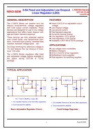
1.5A Ultra Low Dropout Linear Regulator TJ3965
1.5A Ultra Low Dropout Linear Regulator TJ3965
1.5A Ultra Low Dropout Linear Regulator TJ3965
- No tags were found...

You also want an ePaper? Increase the reach of your titles
YUMPU automatically turns print PDFs into web optimized ePapers that Google loves.
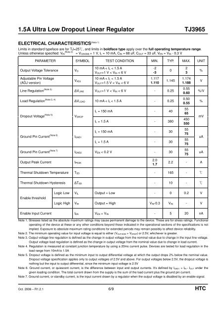
<strong>1.5A</strong> <strong>Ultra</strong> <strong>Low</strong> <strong>Dropout</strong> <strong>Linear</strong> <strong>Regulator</strong><strong>TJ3965</strong>(Note 1)ELECTRICAL CHARACTERISTICSLimits in standard typeface are for TJ=25℃, and limits in boldface type apply over the full operating temperature range.(Note 2)Unless otherwise specified: V IN = V O(NOM) + 1 V, I L = 10 mA, C IN = 68 uF, C OUT = 33 uF, V EN = V IN - 0.3 VPARAMETER SYMBOL TEST CONDITION MIN. TYP. MAX. UNITOutput Voltage ToleranceAdjustable Pin Voltage(ADJ version)V OV ADJ10 mA < I L < 1.5 AV OUT+1 V < V IN < 6 V10 mA < I L < 1.5 AV OUT+1.5 V < V IN < 6 V-2-31.1171.110Line Regulation (Note 3) ∆V LINE V OUT+1 V < V IN < 6 V - 0.25Load Regulation (Note 3, 4) ∆V LOAD 10 mA < I L < 1.5 A - 0.25(Note 5)<strong>Dropout</strong> Voltage V(Note 6)Ground Pin Current IDROPGND101.145I L = 150 mA - 40I L = 1.5 A - 380I L = 150 mA - 30I L = 1.5 A - 30Ground Pin Current (Note 7) I GND2 V EN < 0.2 V - 30Output Peak CurrentI PEAK2.01.7231.1741.1880.550.600.500.555565450550557555755575%V%/V%mVuAuA2.2 - AThermal Shutdown Temperature T SD - 165 -℃Thermal Shutdown Hysteresis ∆T SD - 10 -℃Enable thresholdLogic <strong>Low</strong> V IL Output = <strong>Low</strong> - 0 0.2 VLogic High V IH Output = High V IN-0.3 V IN - VEnable Input Current I EN V EN = V IN - 5 20 nANote 1. Stresses listed as the absolute maximum ratings may cause permanent damage to the device. These are for stress ratings. Functionaloperating of the device at these or any other conditions beyond those indicated in the operational sections of the specifications is notimplied. Exposure to absolute maximum rating conditions for extended periods may remain possibly to affect device reliability.Note 2. The minimum operating value for input voltage is equal to either (V OUT,NOM + V DROP) or 2.5V, whichever is greater.Note 3. Output voltage line regulation is defined as the change in output voltage from the nominal value due to change in the input line voltage.Output voltage load regulation is defined as the change in output voltage from the nominal value due to change in load current.Note 4. Regulation is measured at constant junction temperature by using a 20ms current pulse. Devices are tested for load regulation in theload range from 10mA to <strong>1.5A</strong>Note 5. <strong>Dropout</strong> voltage is defined as the minimum input to output differential voltage at which the output drops 2% below the nominal value.<strong>Dropout</strong> voltage specification applies only to output voltages of 2.5V and above. For output voltages below 2.5V, the dropout voltage isnothing but the input to output differential, since the minimum input voltage is 2.5VNote 6. Ground current, or quiescent current, is the difference between input and output currents. It's defined by I GND1 = I IN - I OUT under thegiven loading condition. The total current drawn from the supply is the sum of the load current plus the ground pin current.Note 7. Ground current, or standby current, is the input current drawn by a regulator when the output voltage is disabled by an enable signal.Oct. 2006 – R1.2.1 6/9 HTC