1.5A Ultra Low Dropout Linear Regulator TJ3965
1.5A Ultra Low Dropout Linear Regulator TJ3965
1.5A Ultra Low Dropout Linear Regulator TJ3965
- No tags were found...

Create successful ePaper yourself
Turn your PDF publications into a flip-book with our unique Google optimized e-Paper software.
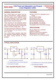
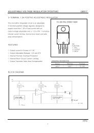
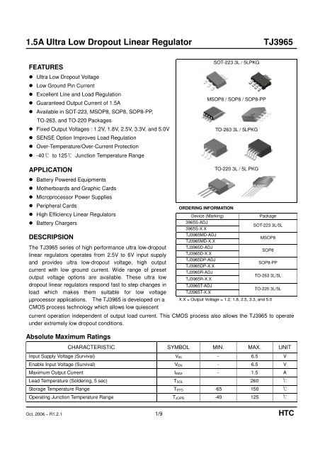
<strong>1.5A</strong> <strong>Ultra</strong> <strong>Low</strong> <strong>Dropout</strong> <strong>Linear</strong> <strong>Regulator</strong><strong>TJ3965</strong>FEATURES <strong>Ultra</strong> <strong>Low</strong> <strong>Dropout</strong> Voltage <strong>Low</strong> Ground Pin Current Excellent Line and Load Regulation Guaranteed Output Current of <strong>1.5A</strong> Available in SOT-223, MSOP8, SOP8, SOP8-PP,TO-263, and TO-220 Packages Fixed Output Voltages : 1.2V, 1.8V, 2.5V, 3.3V, and 5.0V SENSE Option Improves Load Regulation Over-Temperature/Over-Current Protection-40℃ 125℃ to Junction Temperature RangeSOT-223 3L / 5LPKGMSOP8 / SOP8 / SOP8-PPTO-263 3L / 5LPKGAPPLICATION Battery Powered Equipments Motherboards and Graphic Cards Microprocessor Power Supplies Peripheral Cards High Efficiency <strong>Linear</strong> <strong>Regulator</strong>s Battery ChargersDESCRIPSIONThe <strong>TJ3965</strong> series of high performance ultra low-dropoutlinear regulators operates from 2.5V to 6V input supplyand provides ultra low-dropout voltage, high outputcurrent with low ground current. Wide range of presetoutput voltage options are available. These ultra lowdropout linear regulators respond fast to step changes inload which makes them suitable for low voltageORDERING INFORMATIONDevice (Marking)3965S-ADJ3965S-X.X<strong>TJ3965</strong>MD-ADJ<strong>TJ3965</strong>MD-X.X<strong>TJ3965</strong>D-ADJ<strong>TJ3965</strong>D-X.X<strong>TJ3965</strong>DP-ADJ<strong>TJ3965</strong>DP-X.X<strong>TJ3965</strong>R-ADJ<strong>TJ3965</strong>R-X.X<strong>TJ3965</strong>T-ADJ<strong>TJ3965</strong>T-X.XTO-220 3L / 5L PKGPackageSOT-223 3L/5LMSOP8SOP8SOP8-PPTO-263 3L/5LTO-220 3L/5Lµprocessor applications. The <strong>TJ3965</strong> is developed on a X.X = Output Voltage = 1.2, 1.8, 2.5, 3.3, and 5.0CMOS process technology which allows low quiescentcurrent operation independent of output load current. This CMOS process also allows the <strong>TJ3965</strong> to operateunder extremely low dropout conditions.Absolute Maximum RatingsCHARACTERISTIC SYMBOL MIN. MAX. UNITInput Supply Voltage (Survival) V IN - 6.5 VEnable Input Voltage (Survival) V EN - 6.5 VMaximum Output Current I MAX - 1.5 ALead Temperature (Soldering, 5 sec) T SOL 260Storage Temperature Range T STG -65 150Operating Junction Temperature Range T JOPR -40 125℃Oct. 2006 – R1.2.1 1/9 HTC
<strong>1.5A</strong> <strong>Ultra</strong> <strong>Low</strong> <strong>Dropout</strong> <strong>Linear</strong> <strong>Regulator</strong><strong>TJ3965</strong>Ordering InformationV OUT Package Order No. Description Package Marking Supplied AsADJ SOT-223 5L <strong>TJ3965</strong>S-ADJ-5L <strong>1.5A</strong>, Adjustable, Enable 3965-ADJ ReelADJ MSOP8 <strong>TJ3965</strong>MD-ADJ-8L <strong>1.5A</strong>, Adjustable, Enable <strong>TJ3965</strong>-ADJ ReelADJ SOP8 <strong>TJ3965</strong>D-ADJ-8L <strong>1.5A</strong>, Adjustable, Enable <strong>TJ3965</strong>-ADJ ReelADJ SOP8-PP <strong>TJ3965</strong>DP-ADJ-8L <strong>1.5A</strong>, Adjustable, Enable <strong>TJ3965</strong>-ADJ ReelADJ TO-263 5L <strong>TJ3965</strong>R-ADJ-5L <strong>1.5A</strong>, Adjustable, Enable <strong>TJ3965</strong>-ADJ Reel or TubeADJ TO-220 5L <strong>TJ3965</strong>T-ADJ-5L <strong>1.5A</strong>, Adjustable, Enable <strong>TJ3965</strong>-ADJ Tube1.2V SOT-223 3L <strong>TJ3965</strong>S-1.2V-3L <strong>1.5A</strong> 3965-1.2 Reel1.2V SOT-223 5L <strong>TJ3965</strong>S-1.2V-5L <strong>1.5A</strong>, Enable, SENSE 3965-1.2 Reel1.2V MSOP8 <strong>TJ3965</strong>MD-1.2V-8L <strong>1.5A</strong>, Enable, SENSE <strong>TJ3965</strong>-1.2 Reel1.2V SOP8 <strong>TJ3965</strong>D-1.2V-8L <strong>1.5A</strong>, Enable, SENSE <strong>TJ3965</strong>-1.2 Reel1.2V SOP8-PP <strong>TJ3965</strong>DP-1.2-8L <strong>1.5A</strong>, Enable, SENSE <strong>TJ3965</strong>-1.2 Reel1.2V TO-263 3L <strong>TJ3965</strong>R-1.2V-3L <strong>1.5A</strong> <strong>TJ3965</strong>-1.2 Reel or Tube1.2V TO-263 5L <strong>TJ3965</strong>R-1.2V-5L <strong>1.5A</strong>, Enable, SENSE <strong>TJ3965</strong>-1.2 Reel or Tube1.2V TO-220 3L <strong>TJ3965</strong>T-1.2V-3L <strong>1.5A</strong> <strong>TJ3965</strong>-1.2 Tube1.2V TO-220 5L <strong>TJ3965</strong>T-1.2V-5L <strong>1.5A</strong>, Enable, SENSE <strong>TJ3965</strong>-1.2 Tube1.8V SOT-223 3L <strong>TJ3965</strong>S-1.8V-3L <strong>1.5A</strong> 3965-1.8 Reel1.8V SOT-223 5L <strong>TJ3965</strong>S-1.8V-5L <strong>1.5A</strong>, Enable, SENSE 3965-1.8 Reel1.8V MSOP8 <strong>TJ3965</strong>MD-1.8V-8L <strong>1.5A</strong>, Enable, SENSE <strong>TJ3965</strong>-1.8 Reel1.8V SOP8 <strong>TJ3965</strong>D-1.8V-8L <strong>1.5A</strong>, Enable, SENSE <strong>TJ3965</strong>-1.8 Reel1.8V SOP8-PP <strong>TJ3965</strong>DP-1.8V-8L <strong>1.5A</strong>, Enable, SENSE <strong>TJ3965</strong>-1.8 Reel1.8V TO -263 3L <strong>TJ3965</strong>R-1.8V-3L <strong>1.5A</strong> <strong>TJ3965</strong>-1.8 Reel or Tube1.8V TO -263 5L <strong>TJ3965</strong>R-1.8V-5L <strong>1.5A</strong>, Enable, SENSE <strong>TJ3965</strong>-1.8 Reel or Tube1.8V TO-220 3L <strong>TJ3965</strong>T-1.8V-3L <strong>1.5A</strong> <strong>TJ3965</strong>-1.8 Tube1.8V TO-220 5L <strong>TJ3965</strong>T-1.8V-5L <strong>1.5A</strong>, Enable, SENSE <strong>TJ3965</strong>-1.8 Tube2.5V SOT-223 3L <strong>TJ3965</strong>S-2.5V-3L <strong>1.5A</strong> 3965-2.5 Reel2.5V SOT-223 5L <strong>TJ3965</strong>S-2.5V-5L <strong>1.5A</strong>, Enable, SENSE 3965-2.5 Reel2.5V MSOP8 <strong>TJ3965</strong>MD-2.5V-8L <strong>1.5A</strong>, Enable, SENSE <strong>TJ3965</strong>-2.5 Reel2.5V SOP8 <strong>TJ3965</strong>D-2.5V-8L <strong>1.5A</strong>, Enable, SENSE <strong>TJ3965</strong>-2.5 Reel2.5V SOP8-PP <strong>TJ3965</strong>DP-2.5V-8L <strong>1.5A</strong>, Enable, SENSE <strong>TJ3965</strong>-2.5 Reel2.5V TO -263 3L <strong>TJ3965</strong>R-2.5V-3L <strong>1.5A</strong> <strong>TJ3965</strong>-2.5 Reel or Tube2.5V TO -263 5L <strong>TJ3965</strong>R-2.5V-5L <strong>1.5A</strong>, Enable, SENSE <strong>TJ3965</strong>-2.5 Reel or Tube2.5V TO-220 3L <strong>TJ3965</strong>T-2.5V-3L <strong>1.5A</strong> <strong>TJ3965</strong>-2.5 Tube2.5V TO-220 5L <strong>TJ3965</strong>T-2.5V-5L <strong>1.5A</strong>, Enable, SENSE <strong>TJ3965</strong>-2.5 TubeOct. 2006 – R1.2.1 2/9 HTC
<strong>1.5A</strong> <strong>Ultra</strong> <strong>Low</strong> <strong>Dropout</strong> <strong>Linear</strong> <strong>Regulator</strong><strong>TJ3965</strong>Ordering Information(Continued)V OUT Package Order No. Description Package Marking Supplied As3.3V SOT-223 3L <strong>TJ3965</strong>S-3.3V-3L <strong>1.5A</strong> 3965-3.3 Reel3.3V SOT-223 5L <strong>TJ3965</strong>S-3.3V-5L <strong>1.5A</strong>, Enable, SENSE 3965-3.3 Reel3.3V MSOP8 <strong>TJ3965</strong>MD-3.3V-8L <strong>1.5A</strong>, Enable, SENSE <strong>TJ3965</strong>-3.3 Reel3.3V SOP8 <strong>TJ3965</strong>D-3.3V-8L <strong>1.5A</strong>, Enable, SENSE <strong>TJ3965</strong>-3.3 Reel3.3V SOP8-PP <strong>TJ3965</strong>DP-3.3V-8L <strong>1.5A</strong>, Enable, SENSE <strong>TJ3965</strong>-3.3 Reel3.3V TO -263 3L <strong>TJ3965</strong>R-3.3V-3L <strong>1.5A</strong> <strong>TJ3965</strong>-3.3 Reel or Tube3.3V TO -263 5L <strong>TJ3965</strong>R-3.3V-5L <strong>1.5A</strong>, Enable, SENSE <strong>TJ3965</strong>-3.3 Reel or Tube3.3V TO-220 3L <strong>TJ3965</strong>T-3.3V-3L <strong>1.5A</strong> <strong>TJ3965</strong>-3.3 Tube3.3V TO-220 5L <strong>TJ3965</strong>T-3.3V-5L <strong>1.5A</strong>, Enable, SENSE <strong>TJ3965</strong>-3.3 Tube5.0V SOT-223 3L <strong>TJ3965</strong>S-5.0V-3L <strong>1.5A</strong> 3965-5.0 Reel5.0V SOT-223 5L <strong>TJ3965</strong>S-5.0V-5L <strong>1.5A</strong>, Enable, SENSE 3965-5.0 Reel5.0V MSOP8 <strong>TJ3965</strong>MD-5.0V-8L <strong>1.5A</strong>, Enable, SENSE <strong>TJ3965</strong>-5.0 Reel5.0V SOP8 <strong>TJ3965</strong>D-5.0V-8L <strong>1.5A</strong>, Enable, SENSE <strong>TJ3965</strong>-5.0 Reel5.0V SOP8-PP <strong>TJ3965</strong>DP-5.0V-8L <strong>1.5A</strong>, Enable, SENSE <strong>TJ3965</strong>-5.0 Reel5.0V TO -263 3L <strong>TJ3965</strong>R-5.0V-3L <strong>1.5A</strong> <strong>TJ3965</strong>-5.0 Reel or Tube5.0V TO -263 5L <strong>TJ3965</strong>R-5.0V-5L <strong>1.5A</strong>, Enable, SENSE <strong>TJ3965</strong>-5.0 Reel or Tube5.0V TO-220 3L <strong>TJ3965</strong>T-5.0V-3L <strong>1.5A</strong> <strong>TJ3965</strong>-5.0 Tube5.0V TO-220 5L <strong>TJ3965</strong>T-5.0V-5L <strong>1.5A</strong>, Enable, SENSE <strong>TJ3965</strong>-5.0 TubeT J 3 9 6 5 D P – 3.3 V – 8 LLead Count : 3L(Fixed Output Only) / 5L / 8LOutput Voltage : ADJ / 1.2V / 1.8V / 2.5V / 3.3V / 5.0VPackage TypeSMDDDPRT: SOT223: MSOP8: SOP8: SOP8-PP: TO263: TO220Root NameProduct CodeOct. 2006 – R1.2.1 3/9 HTC
<strong>1.5A</strong> <strong>Ultra</strong> <strong>Low</strong> <strong>Dropout</strong> <strong>Linear</strong> <strong>Regulator</strong><strong>TJ3965</strong>PIN CONFIGURATIONSOT223-3L SOT223-5L MSOP8 SOP8 / SOP8-PPTO263-3L TO263-5L TO220-3L TO220-5LPIN DESCRIPTIONPin No.SOT223 / SOT263 / TO220 3 LEADSOT-223 5 LEADName Function Name Function1 V IN Input Supply EN Chip Enable2 GND Ground V IN Input Supply3 V OUT Output Voltage V OUT Output Voltage4 - - SENSE/ADJRemote Senseor Output Adjust5 - - GND GroundPin No.TO263 / TO220 5 LEADMSOP8 / SOP8 / SOP8-PP 8 LEADName Function Name Function1 EN Chip Enable EN Chip Enable2 V IN Input Supply V IN Input Supply3 GND Ground V OUT Output Voltage4 V OUT Output Voltage SENSE/ADJ5 / 6/ 7 / 8 SENSE/ADJRemote Senseor Output AdjustGNDRemote Senseor Output AdjustGroundOct. 2006 – R1.2.1 4/9 HTC
-<strong>1.5A</strong> <strong>Ultra</strong> <strong>Low</strong> <strong>Dropout</strong> <strong>Linear</strong> <strong>Regulator</strong><strong>TJ3965</strong>TYPICAL APPLICATIONTypical 3 Pin ApplicationINPUTV IN<strong>TJ3965</strong>V OUTOUTPUTC IN68μF+GNDC OUT33μFTypical 5 / 8 Pin ApplicationINPUTV IN<strong>TJ3965</strong>- +V OUTOUTPUTC IN68μFENENSENSEGNDC OUT33μF5 / 8 Pin Remote Load Sense+Application-- +INPUTV INV OUTOUTPUTC IN68μF+ENEN<strong>TJ3965</strong>SENSEGND+C OUT33μFOADTypical Adjustable Version ApplicationINPUT-LC IN68μFENV INEN<strong>TJ3965</strong>GNDV OUTADJR 2-1OUTPUTC OUT33μF* <strong>TJ3965</strong> can deliver a continuous current of <strong>1.5A</strong> over the full operating temperature. However, the outputcurrent is limited by the restriction of power dissipation which differs from packages. A heat sink may berequired depending on the maximum power dissipation and maximum ambient temperature of application.With respect to the applied package, the maximum output current of <strong>1.5A</strong> may be still+ +undeliverable.* See Application InformationOct. 2006 – R1.2.1 5/9 HTC-R-
<strong>1.5A</strong> <strong>Ultra</strong> <strong>Low</strong> <strong>Dropout</strong> <strong>Linear</strong> <strong>Regulator</strong><strong>TJ3965</strong>(Note 1)ELECTRICAL CHARACTERISTICSLimits in standard typeface are for TJ=25℃, and limits in boldface type apply over the full operating temperature range.(Note 2)Unless otherwise specified: V IN = V O(NOM) + 1 V, I L = 10 mA, C IN = 68 uF, C OUT = 33 uF, V EN = V IN - 0.3 VPARAMETER SYMBOL TEST CONDITION MIN. TYP. MAX. UNITOutput Voltage ToleranceAdjustable Pin Voltage(ADJ version)V OV ADJ10 mA < I L < 1.5 AV OUT+1 V < V IN < 6 V10 mA < I L < 1.5 AV OUT+1.5 V < V IN < 6 V-2-31.1171.110Line Regulation (Note 3) ∆V LINE V OUT+1 V < V IN < 6 V - 0.25Load Regulation (Note 3, 4) ∆V LOAD 10 mA < I L < 1.5 A - 0.25(Note 5)<strong>Dropout</strong> Voltage V(Note 6)Ground Pin Current IDROPGND101.145I L = 150 mA - 40I L = 1.5 A - 380I L = 150 mA - 30I L = 1.5 A - 30Ground Pin Current (Note 7) I GND2 V EN < 0.2 V - 30Output Peak CurrentI PEAK2.01.7231.1741.1880.550.600.500.555565450550557555755575%V%/V%mVuAuA2.2 - AThermal Shutdown Temperature T SD - 165 -℃Thermal Shutdown Hysteresis ∆T SD - 10 -℃Enable thresholdLogic <strong>Low</strong> V IL Output = <strong>Low</strong> - 0 0.2 VLogic High V IH Output = High V IN-0.3 V IN - VEnable Input Current I EN V EN = V IN - 5 20 nANote 1. Stresses listed as the absolute maximum ratings may cause permanent damage to the device. These are for stress ratings. Functionaloperating of the device at these or any other conditions beyond those indicated in the operational sections of the specifications is notimplied. Exposure to absolute maximum rating conditions for extended periods may remain possibly to affect device reliability.Note 2. The minimum operating value for input voltage is equal to either (V OUT,NOM + V DROP) or 2.5V, whichever is greater.Note 3. Output voltage line regulation is defined as the change in output voltage from the nominal value due to change in the input line voltage.Output voltage load regulation is defined as the change in output voltage from the nominal value due to change in load current.Note 4. Regulation is measured at constant junction temperature by using a 20ms current pulse. Devices are tested for load regulation in theload range from 10mA to <strong>1.5A</strong>Note 5. <strong>Dropout</strong> voltage is defined as the minimum input to output differential voltage at which the output drops 2% below the nominal value.<strong>Dropout</strong> voltage specification applies only to output voltages of 2.5V and above. For output voltages below 2.5V, the dropout voltage isnothing but the input to output differential, since the minimum input voltage is 2.5VNote 6. Ground current, or quiescent current, is the difference between input and output currents. It's defined by I GND1 = I IN - I OUT under thegiven loading condition. The total current drawn from the supply is the sum of the load current plus the ground pin current.Note 7. Ground current, or standby current, is the input current drawn by a regulator when the output voltage is disabled by an enable signal.Oct. 2006 – R1.2.1 6/9 HTC
<strong>1.5A</strong> <strong>Ultra</strong> <strong>Low</strong> <strong>Dropout</strong> <strong>Linear</strong> <strong>Regulator</strong>TYPICAL OPERATING CHARACTERISTICS<strong>TJ3965</strong>Ambient Temperature vs. Output Voltage ChangeOutput Current vs. <strong>Dropout</strong> VoltagePower Dissipation vs. Case Temperature, MSOP8Power Dissipation vs. Case Temperature, SOP8Power Dissipation vs. Case Temperature, SOP8-PPT.B.D.Oct. 2006 – R1.2.1 7/9 HTC
<strong>1.5A</strong> <strong>Ultra</strong> <strong>Low</strong> <strong>Dropout</strong> <strong>Linear</strong> <strong>Regulator</strong>APPLICATION INFORMATION<strong>TJ3965</strong>Output Adjustment (Adjustable Version)An adjustable output device has output voltage range of 1.145V to 5.0V. To obtain a desired outputvoltage, the following equation can be used with R1 resistor range of 10kΩ to 220kΩ⎛ V ⎞= R1⎜− 1⎟⎝1.145⎠2OUTTo enhance output stability, a capacitor of 68pF to 100pF can be placed in series with V OUT and ADJ.SENSE PinIn applications where the regulator output is not very close to the load, the <strong>TJ3965</strong> can provide betterremote load regulation characteristics using the SENSE pin. <strong>TJ3965</strong> regulates the voltage at the outputpin. Hence, the voltage at the remote load will be lower than the voltage at the output pin as a value ofthe voltage drop across the trace series resistance. If the sense option pin is not required, the sense pinmust be connected to the V OUT pin. Connecting the sense pin to the remote load will provide regulationat the remote load because the <strong>TJ3965</strong> regulates the voltage at the sense pin when the sense option pinis used.RMaximum Output Current CapabilityThe <strong>TJ3965</strong> can deliver a continuous current of <strong>1.5A</strong> over the full operating junction temperature range.However, the output current is limited by the restriction of power dissipation which differs from packages.A heat sink may be required depending on the maximum power dissipation and maximum ambienttemperature of application. With respect to the applied package, the maximum output current of <strong>1.5A</strong>may be still undeliverable due to the restriction of the power dissipation of <strong>TJ3965</strong>. Under all possibleconditions, the junction temperature must be within the range specified under operating conditions.The temperatures over the device are given by:T C = T A + P D X θ CAT J = T C + P D X θ JCT J = T A + P D X θ JAwhere T J is the junction temperature, T C is the case temperature, T A is the ambient temperature, P D is thetotal power dissipation of the device, θ CA is the thermal resistance of case-to-ambient, θ JC is the thermalOct. 2006 – R1.2.1 8/9 HTC
<strong>1.5A</strong> <strong>Ultra</strong> <strong>Low</strong> <strong>Dropout</strong> <strong>Linear</strong> <strong>Regulator</strong><strong>TJ3965</strong>resistance of junction-to-case, and θ JA is the thermal resistance of junction to ambient.The total power dissipation of the device is given by:P D = P IN – P OUT = (V IN X I IN )–(V OUT X I OUT )= (V IN X (I OUT +I GND )) – (V OUT X I OUT ) = (V IN - V OUT ) X I OUT + V IN X I GNDwhere I GND is the operating ground current of the device which is specified at the Electrical Characteristics.The maximum allowable temperature rise (T Rmax ) depends on the maximum ambient temperature (T Amax )of the application, and the maximum allowable junction temperature (T Jmax ):T Rmax = T Jmax – T AmaxThe maximum allowable value for junction-to-ambient thermal resistance, θ JA , can be calculated using theformula:θ JA = T Rmax / P D<strong>TJ3965</strong> is available in SOT223, MSOP8, SOP8-PP, TO263, and TO220 packages. The thermalresistance depends on amount of copper area or heat sink, and on air flow. If the maximum allowablevalue of θ JA calculated above is over 140°C/W for SO-223 package, over 220°C/W for MSOP8 package,over 165°C/W for SOP8 package, over 170°C/W for SOP8-PP package, over 80 °C/W for TO263package, over 75 °C/W for TO220 package, no heat sink is needed since the package can dissipateenough heat to satisfy these requirements. If the value for allowable θ JA falls near or below these limits,a heat sink or proper area of copper plane is required.In summary, the absolute maximum ratings of thermal resistances are as follow:Absolute Maximum Ratings of Thermal ResistanceNo heat sink / No air flow / No adjacent heat source / T A = 25°CCharacteristic Symbol Max. Rating UnitThermal Resistance Junction-To-Ambient / SOT223 θ JA-SOT223 140 °C/WThermal Resistance Junction-To-Ambient / MSOP8 θ JA-MSOP8 220 °C/WThermal Resistance Junction-To-Ambient / SOP8 θ JA-SOP8 165 °C/WThermal Resistance Junction-To-Ambient / SOP8-PP θ JA-SOP8-PP 175 °C/WThermal Resistance Junction-To-Ambient / TO263 θ JA-TO263 80 °C/WThermal Resistance Junction-To-Ambient / TO220 θ JA-TO220 75 °C/WT.B.D.Oct. 2006 – R1.2.1 9/9 HTC