Preliminary Program - The Society of Vacuum Coaters
Preliminary Program - The Society of Vacuum Coaters
Preliminary Program - The Society of Vacuum Coaters
- No tags were found...

You also want an ePaper? Increase the reach of your titles
YUMPU automatically turns print PDFs into web optimized ePapers that Google loves.
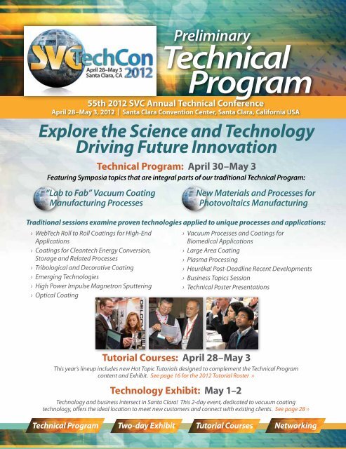
› WebTech Roll to Roll Coatings for High-EndApplications› Coatings for Cleantech Energy Conversion,Storage and Related Processes› Tribological and Decorative Coating› Emerging Technologies› High Power Impulse Magnetron Sputtering› Optical Coating<strong>Preliminary</strong>Technical<strong>Program</strong>55th 2012 SVC Annual Technical ConferenceApril 28–May 3, 2012 | Santa Clara Convention Center, Santa Clara, California USAExplore the Science and TechnologyDriving Future InnovationTechnical <strong>Program</strong>: April 30–May 3Featuring Symposia topics that are integral parts <strong>of</strong> our traditional Technical <strong>Program</strong>:“Lab to Fab” <strong>Vacuum</strong> CoatingManufacturing ProcessesNew Materials and Processes forPhotovoltaics ManufacturingTraditional sessions examine proven technologies applied to unique processes and applications:› <strong>Vacuum</strong> Processes and Coatings forBiomedical Applications› Large Area Coating› Plasma Processing› Heuréka! Post-Deadline Recent Developments› Business Topics Session› Technical Poster PresentationsTutorial Courses: April 28–May 3This year’s lineup includes new Hot Topic Tutorials designed to complement the Technical <strong>Program</strong>content and Exhibit. See page 16 for the 2012 Tutorial Roster ››Technology Exhibit: May 1–2Technology and business intersect in Santa Clara! This 2-day event, dedicated to vacuum coatingtechnology, <strong>of</strong>fers the ideal location to meet new customers and connect with existing clients. See page 28 ››Technical <strong>Program</strong> Two-day Exhibit Tutorial Courses Networking
2012 Technical <strong>Program</strong>University <strong>of</strong> Technology, Eindhoven, <strong>The</strong>Netherlands11:50 a.m. PV-7 New Approaches <strong>of</strong> Controlling<strong>of</strong> Electrical and Optical Properties <strong>of</strong> DCSputtered Al Doped ZnO Thin Film for TransparentConducting OxideW. Yang and J. Joo, Kunsan National University,Kunsan, South KoreaTribological and Decorative CoatingModerators: Jolanta Klemberg-Sapieha, ÉcolePolytechnique de Montréal, Canada and KlausBewilogua, Fraunh<strong>of</strong>er Institute for SurfaceEngineering and Thin Films IST, GermanyInvited speaker9:10 a.m. T-1 In Situ Tribometry: SheddingLight on the Tribology <strong>of</strong> Hard CoatingsR.R. Chromik and H.W. Strauss, Department <strong>of</strong>Mining and Materials Engineering, McGill University,Montréal, Canada; and S. Hassani andJ.E. Klemberg-Sapieha, École Polytechnique deMontréal, Montréal, Canada9:50 a.m. T-2 Properties <strong>of</strong> TiN Films Preparedby Oblique Angle DepositionJ.I. Jeong, J.H. Yang, J.H. Jung, H.S. Park, andM.A. Song, Hybrid Materials Research Department,Research Institute <strong>of</strong> Industrial Scienceand Technology, Pohang, Korea10:10 a.m. – 10:30 a.m. – Break10:30 a.m. T-3 Deposition <strong>of</strong> Thick a-C:H:SiCoatings for Tribological ApplicationsC. Forsich, University <strong>of</strong> Applied Sciences, Wels,Austria; D. Heim, Upper University <strong>of</strong> AppliedSciences, Wels, Austria; and T. Mueller and A.Gebeshuber, Rübig GmbH & Co KG Anlagentechnik,Wels, Austria10:50 a.m. T-4 Silicon Aluminum OxynitrideThin Films Deposited by Plasma EnhancedChemical Vapour DepositionSponsored Student PresentationO. Taggart and P. Masher, Department <strong>of</strong> EngineeringPhysics, McMaster University, Hamilton,Canada; L. Martinu, Department <strong>of</strong> EngineeringPhysics, École Polytechnique de Montréal, Montréal,Canada; J. Wojcik, Department <strong>of</strong> EngineeringPhysics, McMaster University, Hamilton,Canada; J.E. Klemberg-Sapieha, Department <strong>of</strong>Engineering Physics, École Polytechnique deMontréal, Montréal, Canada11:10 a.m. T-5 High Performance PVD Coatingsfor Today’s and Tomorrow’s Engine PlatformsR. Jacobs, Hauzer Techno Coating BV, Venlo, <strong>The</strong>Netherlands; T. Liskiewicz and L. Austin, School<strong>of</strong> Mechanical Engineering, University <strong>of</strong> Leeds,Leeds, United Kingdom; D. Doerwald and R.Tietema, Hauzer Techno Coating BV, Venlo, <strong>The</strong>Netherlands; A. Neville, School <strong>of</strong> MechanicalEngineering, University <strong>of</strong> Leeds, Leeds, UnitedKingdom; and T. Krug, Hauzer Techno CoatingBV, Venlo, <strong>The</strong> Netherlands11:30 a.m. T-6 Nanostructured PVD Coating forHigh Demanded ApplicationsJ.A. Araujo, Metallurgical and Materials EngineeringDepartment, University <strong>of</strong> São Paulo,São Paulo, Brazil; G.M. Araujo, MAHLE-TechnologyCenter Brazil, São Paulo, Brazil; and A.Tschiptschin, Department <strong>of</strong> Metallurgical andMaterials Engineering, São Paulo University, SãoPaulo, Brazil11:50 a.m. T-7 Modified Diamond-Like CarbonMultilayer Coatings on Metallic SubstratesProduced by Pulsed-DC Hollow Cathode PECVDSponsored Student PresentationR. Birney and F. Placido, Thin Film Centre, University<strong>of</strong> the West <strong>of</strong> Scotland, Paisley, UnitedKingdomPlasma ProcessingModerators: James Bradley, University <strong>of</strong>Liverpool, United Kingdom and Jorg Patscheider,EMPA, Switzerland9:10 a.m. P-1 Effects <strong>of</strong> Cumulative SurfaceTreatment on <strong>Vacuum</strong>-Deposited CoatingAdhesionR. Wolf, Enercon Industries Corporation,Menomonee Falls, WI; C.A. Bishop, C.A. BishopConsulting Ltd, Near Loughborogh, UnitedKingdom; and I. Fletcher, Intertek MSG, Redcar,United Kingdom9:30 a.m. P-2 Influence <strong>of</strong> Deposition Parametersin PACVD-SiO 2Preparation on ResultingFilm PropertiesR. Bandorf, Fraunh<strong>of</strong>er Institute for SurfaceEngineering and Thin Films IST, Braunschweig,Germany; I. Stasewitsch, Insitut für Oberflächentechnik,TU-Braunschweig, Braunschweig,Germany; H. Gerdes, Fraunh<strong>of</strong>er Institute forSurface Engineering and Thin Films IST, Braunschweig,Germany; and G. Bräuer, Fraunh<strong>of</strong>erInstitute for Surface Engineering and Thin FilmsIST, Braunschweig, Germany and Insitut fürOberflächentechnik, TU-Braunschweig, Braunschweig,Germany9:50 a.m. P-3 Plasma-Based Chemical Modification<strong>of</strong> Epitaxial GrapheneS.C. Hernández, M. Baraket, and E.H. Lock,Plasma Physics Division, U.S. Naval ResearchLaboratory, Washington, DC; V.D. Wheeler, L.O.Nyakiti, F.J. Bezares, R.L. Myers-Ward, C.R. EddyJr., D.K. Gaskill, and J.D. Caldwell, ElectronicsScience and Technology Division, U.S. NavalResearch Laboratory, Washington, DC; and S.G.Walton, Plasma Physics Division, U.S. NavalResearch Laboratory, Washington, DC10:10 a.m. – 10:30 a.m. – Break10:30 a.m. P-4 Magnetron Assisted PECVD Processfor Deposition <strong>of</strong> a-Si:H and µc-Si:H from aSilane-Hydrogen-Argon Gas MixtureP. Pötschick, H. Bartzsch, A. Delan, and P. Frach,Fraunh<strong>of</strong>er Institute for Electron Beam andPlasma Technology FEP, Dresden, GermanyTechnology Forum BreakfastTopics and FacilitatorsMonday, April 307:00 a.m. – 8:15 a.m.Coatings for Thin FilmPhotovoltaics – Wolfgang Diehl andVolker Sittinger, Fraunh<strong>of</strong>er Institute for SurfaceEngineering and Thin Films IST, GermanyHigh-Power Impulse Magnetron Sputtering(HIPIMS) – Arutiun P. Ehiasarian, SheffieldHallam University, United Kingdom andRalf Bandorf, Fraunh<strong>of</strong>er Institute for SurfaceEngineering and Thin Films IST, GermanyTransparent Conductive Oxides (TCO)for Thin Film Photovoltaics, Displays,Transparent Electronics and More – ClarkBright, 3M CompanyOptical Coating Design – H. Angus Macleod,Thin Film Center Inc.Tribological Coatings – Allan Matthews,University <strong>of</strong> Sheffield, United Kingdom andBill Sproul, Reactive Sputtering, Inc.10:50 a.m. P-5 Alternative Methods for Deposition<strong>of</strong> Superhydrophobic FluorocarbonCoatingsH. Biederman, O. Kylian, M. Petr, M. Drabik,A. Serov, O. Polonskyi, P. Solar, A. Artemenko,A. Choukourov, J. Kousal, D. Arzhakov, and D.Slavinska, Charles University in Prague, Prague,Czech Republic11:10 a.m. P-6 Nanorough Surfaces PreparedUsing Gas Aggregation Cluster SourcesSponsored Student PresentationP. Solar, O. Polonskyi, M. Petr, O. Kylian, A.Artemenko, A. Choukourov, D. Arzhakov, D.Slavinska, and H. Biederman, Charles Universityin Prague, Prague, Czech Republic11:30 a.m. P-7 High Quality Low TemperaturePlasma Deposition <strong>of</strong> Aluminum Oxide Thin FilmsSponsored Student PresentationA. Jagia, Department <strong>of</strong> Applied Physics, EindhovenUniversity <strong>of</strong> Technology, Eindhoven, <strong>The</strong>Netherlands; M.C.M van de Sanden, Department<strong>of</strong> Applied Physics, Eindhoven University <strong>of</strong>Technology, Eindhoven, <strong>The</strong> Netherlands andOM Institute for Plasma Physics, Nieuwegein,<strong>The</strong> Netherlands; J. Michels, TNO Holst Centre,Eindhoven, <strong>The</strong> Netherlands; and M. Creatore,Department <strong>of</strong> Applied Physics, EindhovenUniversity <strong>of</strong> Technology, Eindhoven, <strong>The</strong> Netherlands11:50 a.m. P-8 Examples <strong>of</strong> Plasma Treatment<strong>of</strong> Organic SubstancesP. Kríz, Department <strong>of</strong> Applied Physics andTechnology, University <strong>of</strong> South Bohemia,Ceské Budejovice, Czech Republic; P. Spatenka,Department <strong>of</strong> Applied Physics and Technology,505/856-7188 Fax 505/856-6716 » E-mail svcinfo@svc.org » Web Site www.svc.org5
2012 Technical <strong>Program</strong>University <strong>of</strong> South Bohemia, Ceské Budejovice,Czech Republic and Department <strong>of</strong> MaterialScience, Technical Univerzity <strong>of</strong> Liberec, Liberec,Czech Republic; J. Cerman, Department <strong>of</strong>Material Science, Technical Univerzity <strong>of</strong> Liberec,Liberec, Czech Republic; M. Dienstbier, ResearchMonday Afternoon, April 30<strong>The</strong> Donald M. Mattox Tutorial<strong>Program</strong>12:50 p.m. – 1:35 p.m.See this page for detailsKeynote Presentation1:50 p.m. – 2:30 p.m.Some Implications <strong>of</strong> “Nanotech” OnTransitioning From Lab to MarketPresented by Robert Praino, ChasmTechnologies, Canton, MASee abstract and biographical sketch on page 7.Symposium on “Lab to Fab” <strong>Vacuum</strong>Coating Manufacturing ProcessesModerator: Carl Lampert, Star Science2:30 p.m. L2F-1 High Throughput AtomicLayer Deposition <strong>of</strong> Al 2O 3for Ultrabarrier Encapsulation<strong>of</strong> Large Area ElectronicsJ.C.S. Kools, Encapsulix SAS, Simiane, France2:50 p.m. L2F-2 Electrical, Optical Properties<strong>of</strong> Indium-Tin-Oxide Films Deposited on PolyethyleneTerephthalate Substrate for CapacitiveTouch Panels6Donald M. Mattox Tutorial <strong>Program</strong><strong>Society</strong> <strong>of</strong> <strong>Vacuum</strong> <strong>Coaters</strong> » 2012 TechCon <strong>Preliminary</strong> <strong>Program</strong>Institute <strong>of</strong> Brewing and Malting, Prague, CzechRepublic; B. Gavril, Technical University “Gh.Asachi”, Iasi, Romania; and B. Será, Institute<strong>of</strong> Nanobiology and Structural Biology GCRC,Academy <strong>of</strong> Sciences <strong>of</strong> the Czech Republic,Ceské Budejovice, Czech RepublicMonday Afternoon, April 3012:50 p.m.– 1:35 p.m.Emerging Trends in Solid State LightingPresented by Julian Carey, Intematix, Freemont, CAThis talk will focus on the emerging trends in the solid state lighting industryand the growing demand for efficient high quality lighting solutions. Also discussedwill be how innovative phosphor and remote phosphor materials areimproving LED lighting designs as more manufacturers begin to develop LEDlighting solutions to replace incandescent bulbs and fixtures used in generallighting applications. This presentation will include a discussion on lightingsystem efficacy comparisons between a white LED system and a remotephosphor system using a blue LED to improve light quality. Additionally, thisdiscussion will highlight how these latest innovations in LED lighting technology have risen to thechallenge to make light bulbs, fixtures, TVs and displays brighter and more efficient.Julian Carey is marketing director at Intematix, a leading innovator <strong>of</strong> patented phosphors and phosphor componentsfor high-quality LED lighting. Prior to joining Intematix, Julian directed product management and corporatebranding for Prysm, a maker <strong>of</strong> Laser Phosphor Displays. In the lighting area, Julian was VP <strong>of</strong> Marketing at LUXIMwhere he launched plasma lighting products for OEMs in consumer TV, commercial display and general lightingapplications. Previously, he served as product marketing manager at Philips Lumileds Lighting where he led thecommercialization <strong>of</strong> their LED product family into diverse markets including cell phone camera flash, printing andimaging, signage and general lighting. Prior to Philips, Julian held product design and process engineering rolesdeveloping the first family <strong>of</strong> power LEDs and systems at the Optoelectronics Division <strong>of</strong> Hewlett-Packard. He holds aBS degree in mechanical engineering from Stanford University and an MBA from MIT Sloan.D.-H. Kim, Toray Advanced Materials Korea Inc.,Seoul, South Korea; J.-Y. Park, Toray AdvancedMaterials Korea Inc., Gumi, South Korea; and H.-S. Jeon and Y.-S. Kim, Toray Advanced MaterialsKorea Inc., Seoul, South Korea3:10 p.m. L2F-3 Compact <strong>Vacuum</strong> Web CoatingSystem for R&DH. Tamagaki and T. Segawa, Kobe Steel, Ltd.,Takasago, Japan3:30 p.m. – 3:50 p.m. - BreakInvited speakerContributed by the Emerging Technologies TAC3:50 p.m. L2F-4 Depositing Copper onFlexible Polymers with the Help <strong>of</strong> a Nano-CoatingA.N. Beavers, Jr., SRI International, Menlo Park, CA4:30 p.m. L2F-5 Innovative Automated WebInspection Systems - Vision Beyond DefectDetection in <strong>Vacuum</strong> Coating ManufacturingProcessesJ. Koenig, Schenk Vision, Woodbury, MNInvited speakerContributed by the Optical Coating TAC4:50 p.m. L2F-6 Recent Advances in MultilayerPolymeric Interference ReflectorsM.F. Weber, 3M Company, St. Paul, MNLarge Area CoatingModerator: Michael Andreasen, <strong>Vacuum</strong> EdgeInvited speaker2:30 p.m. L-1 Advanced Transparent Contactsfor Photovoltaic and Other ApplicationsT.M. Barnes, J. Burst, J.L. Blackburn, and T.Gessert, National Renewable Energy Laboratory,Golden, CO3:10 p.m. L-2 Recent Developments <strong>of</strong>TiO 2:Nb Sputtered with High Deposition Ratesfrom a Rotatable Magnetron SystemM. Junghähnel and F. Fietzke, Fraunh<strong>of</strong>er Institutefor Electron Beam and Plasma TechnologyFEP, Dresden, Germany; and M. Vinnichenkoand S. Cornelius, Helmholtz-Zentrum Dresden-Rossendorf, Dresden, Germany3:30 p.m. – 3:50 p.m. - Break3:50 p.m. L-3 ITO 97/3 Coatings as TransparentContact for Heterojunction C-Si Solar CellsP. Lippens and M. Büchel, UMICORE Thin FilmsProducts, Balzers, Principality <strong>of</strong> Liechtenstein;and C. Szepesi and J. Fargo, UMICORE Thin FilmProducts USA, Providence, RI4:10 p.m. L-4 Structural and ElectricalProperties <strong>of</strong> Highly Transparent ConductiveGa-Doped ZnO Films by Magnetron SputteringK. Nagamoto, T. Hara, and T. Kondo, ResearchCenter, LINTEC Corporation, Saitama, Japan;and K. Ishi, Utsunomiya University, Tochigi,Japan4:30 p.m. L-5 Large Area PECVD CoatingsCombined In-Line with SputteringW. Seaman and J. Madocks, General Plasma,Tucson, Arizona4:50 p.m. L-6 In-Line Hot-Wire ChemicalVapor Deposition <strong>of</strong> Silicon-Based CoatingsL. Schaefer, T. Harig, M. Hoefer, and A. Laukart,Fraunh<strong>of</strong>er Institute for Surface Engineeringand Thin Films IST, Braunschweig, Germany; D.Borchert and S. Keipert-Colberg, Fraunh<strong>of</strong>erInstitute for Solar Energy Systems ISE, Gelsenkirchen,Germany; and J. Trube, Leybold Optics,Alzenau, Germany5:10 p.m. L-7 Plasma-Activated Electron BeamPhysical Vapor Deposition - Novel Technologiesand ToolsG. Mattausch, B. Scheffel, C. Metzner, and F.-H.Roegner, Fraunh<strong>of</strong>er Insitute for Electron Beamand Plasma Technology FEP, Dresden, GermanyHigh Power Impulse MagnetronSputtering - HIPIMSModerator: Ralf Bandorf, Fraunh<strong>of</strong>er Institutefor Surface Engineering and Thin Films IST,GermanyInvited speaker2:30 p.m. HP-1 Hard Coatings for AdvancedCutting Tool Applications Produced byHiPIMS-Technology
2012 Technical <strong>Program</strong>O. Lemmer, C. Schiffers, S. Bolz, and W. Kölker,CemeCon AG, Würselen, Germany; and G.Greczynski and L. Hultman, Department <strong>of</strong>Physics, Linköping University, Linköping,Finland3:10 p.m. HP-2 Effect <strong>of</strong> the Degree <strong>of</strong> HIPIMSUtilisation on the Properties <strong>of</strong> TiN FilmsP.Eh. Hovsepian, A.A. Sugumaran, Y. Purandare,and A.P. Ehiasarian, Sheffield Hallam University,Sheffield, United Kingdom3:30 p.m. – 3:50 p.m. - Break3:50 p.m. HP-3 Reactive HIPIMS Sputter Deposition<strong>of</strong> Alumina from Industrial Size RotatablesH. Gerdes, R. Bandorf, and G. Bräuer, Fraunh<strong>of</strong>erInstitute for Surface Engineering and Thin FilmsIST, Braunschweig, Germany4:10 p.m. HP-4 Pulse Magnetron Sputteringwith High Power Density - Process and FilmPropertiesP. Frach, C. Gottfried, F. Fietzke, H. Klostermann,H. Bartzsch, and D. Glöß, Fraunh<strong>of</strong>er Institutefor Electron Beam and Plasma Technology FEP,Dresden, Germany4:30 p.m. HP-5 Modeling <strong>of</strong> High PowerImpulse Magnetron Sputtering <strong>of</strong> CopperSponsored Student PresentationT. Kozák, Department <strong>of</strong> Physics, University <strong>of</strong>West Bohemia, Plzen, Czech Republic4:50 p.m. HP-6 Azimuthal Ion Spin in HiPIMSDischargesJ.W. Bradley, P. Poolcharuansin, and B. Liebig,Department <strong>of</strong> Electrical Engineering andElectronics, University <strong>of</strong> Liverpool, Liverpool,United Kingdom5:10 p.m. HP-7 Inductively Coupled ImpulseSputtering (ICIS): A Novel Technique for IonisedPVDA.P. Ehiasarian and D.A.L. Loch, HIPIMS TechnologyCentre, Sheffield Hallam University, Sheffield,United KingdomEmerging TechnologiesModerators: Chris Stoessel, Southwall Technologiesand Clark Bright, 3M Company2:30 p.m. E-1 Transfer Print <strong>of</strong> Single LayerGraphene to PolymersE.H. Lock and S.C. Hernández, Plasma PhysicsDivision, U.S. Naval Research Laboratory,Washington, DC; M. Laskoski, S. Mulvaney, V.D.Wheeler, and W.K. Lee, Chemistry Division, U.S.Naval Research Laboratory, Washington, DC; T.Anderson, F.J. Bezares, F.J. Kulb, J.D. Caldwell,and K.D. Hobart, Electronics Division, U.S. NavalResearch Laboratory, Washington, DC; P.E. Sheehan,Chemistry Division, U.S. Naval ResearchLaboratory, Washington, DC; B.N. Feygelson,L.O. Nyakiti, R.L. Myers-Ward, C.R. Eddy Jr., andD.K. Gaskill, Electronics Division, U.S. Naval ResearchLaboratory, Washington, DC; S.G. Walton,Plasma Physics Division, U.S. Naval ResearchLaboratory, Washington, DCKeynote SpeakerSymposium on “Lab to Fab” <strong>Vacuum</strong> Coating Manufacturing ProcessesMonday Afternoon, April 30 at 1:50 p.m. – 2:30 p.m.Some Implications <strong>of</strong> “Nanotech” On Transitioning From Lab to MarketPresented by Robert F. Praino, Jr., Co-Founder Chasm Technologies, Inc.,Canton, MAFrequent reference is made to the “valley <strong>of</strong> death” and “bridging the gap” forboth new companies and existing ones. In the case <strong>of</strong> the new company, i.e.a startup less than five years old, there are unique barriers that must be overcome.It turns out that size matters relative to materials processing, evaluation,and understanding, and the “age <strong>of</strong> nanotechnology” has unanticipated effects.<strong>The</strong> ability to rapidly develop and deliver a product to paying customersis a dominant driver for a young organization. For a new technology platform, a new material, or“disruptive” device, the tension can be exacerbated between technology validation/acceptance andthe need to break into existing supply chains or market arenas. This talk will explore some <strong>of</strong> theencounters experienced by startups within the nanotech space. Although a traditional “stage-gate”development framework can be effective as a means to manage the development process, certainmodifications and adjustments can facilitate greater success. Early integration <strong>of</strong> strategy and tacticscan help to make the journey easier.Mr. Praino has 35 years <strong>of</strong> experience developing and manufacturing products utilizing film coating processes. Hiscareer path prior to Chasm includes assignments at Stone & Webster Engineering, Polaroid Corporation, Presstek, VitexSystems, and Precision Lithograining. Bob has a BS and MS in Chemical Engineering from Worcester PolytechnicInstitute and MBA from Boston University. He co-founded Chasm in March 2005 to apply his experience in coatedfilm products and associated science and engineering to develop commercially viable pathways to product applicationsbeginning with a wide range <strong>of</strong> “nano-materials” and “nano-technologies”. <strong>The</strong> applications for these technicalareas have included flat panel displays, fuel cells, photovoltaics, film substrate development, optical film development,carbon nanotube applications, life sciences, and nano-imprint lithography. In addition to the process work inthese areas, Chasm has designed and managed capital equipment projects totaling over $10 million for roll-to-rollcoating lines and nano-material manufacturing facilities.2:50 p.m. E-2 Large Area PECVD Process UsingDual Rotatable MagnetronsM. Fahland, J. Neidhardt, R. Thielsch, A. Wahl,R. Kleinhempel, R. Bluethner, and T. Preussner,Fraunh<strong>of</strong>er Institute for Electron Beam andPlasma Technology FEP, Dresden, Germany3:10 p.m. E-3 “Save Art” Treatment: New Improvementsin Removable-Protective Coatingsfor Metallic Archaeological FindsC. Misiano, P. Matarazzo and M. Pezzilli, RomanaFilm Sottili, Anzio Italy; E. Bemporad and L.Mazzola, University <strong>of</strong> Roma 3, Rome, Italy; andE. Angelini and S. Grassini, Politecnico di Torino,Torino, Italy3:30 p.m. – 3:50 p.m. - BreakInvited speaker3:50 p.m. E-4 Advances in Roll to Roll AtomicLayer DepositionE.R. Dickey, Lotus Applied Technology,Hillsboro, OR4:30 p.m. E-5 Water Vapor Transmission Ratesfor Ultrabarriers on Polymers Grown UsingAtomic Layer DepositionJ.A. Bertrand and S.M. George, Departments <strong>of</strong>Chemistry and Chemical Engineering, University<strong>of</strong> Colorado, Boulder, CO4:50 p.m. E-6 New Design and Operation <strong>of</strong>Photon Energy Source for the Low TemperatureAtomic Layer Deposition Process; Deposition <strong>of</strong>TiO 2on Polymer SubstratesT.O. Kääriäinen, M.-L. Kääriäinen and D.C.Cameron, ASTRaL, Lappeenranta University <strong>of</strong>Technology, Mikkeli, Finland5:10 p.m. E-7 Flexible Phosphorescent OLEDLighting Devices Encapsulated with a NovelThin Film BarrierP. Mandlik, J. Silvernail, K. Rajan, P. Levermore,H. Pang, E. Krall, R. Ma, and J.J. Brown, UniversalDisplay Corporation, Ewing, NJMonday Evening, April 30Heuréka! Post Deadline RecentDevelopments Session6:00 p.m.Moderators: Hana Baránková and LadislavBárdos, Uppsala University, SwedenSVC will continue to accept abstracts for theHeuréka! Session through March 2, 2012Designing and Building a R&D <strong>Vacuum</strong> CoatingTool from Standard Catalog ComponentsJ. Moore, MDC <strong>Vacuum</strong> Products, LLC.,Hayward, CAA Self Cleaning Continuous Process FilmThickness Monitor for OLED, CIGS and OrganicCompound <strong>Vacuum</strong> DepositionsS. Grimshaw, Colnatec, Gilbert, AZ505/856-7188 Fax 505/856-6716 » E-mail svcinfo@svc.org » Web Site www.svc.org7
2012 Technical <strong>Program</strong>9:50 a.m. P-10 Discharge Behavior andDeposition <strong>of</strong> DLC Film in High Power PulsedMagnetron Discharge ConfigurationX. Tian, Z. Wu, G. Gui, C. Gong, and S. Yang,State Key Laboratory <strong>of</strong> Advanced Welding andJoining, Harbin Institute <strong>of</strong> Technology, Harbin,China; and P.K. Chu, Department <strong>of</strong> Physics andMaterials Science, City University <strong>of</strong> Hong Kong,Hong Kong, China10:10 a.m. – 10:30 a.m. – BreakPlasma Processing10:30 a.m. P-11 2-D Spatial Maps <strong>of</strong> NegativeIon Densities and Temperatures in Oxygen/ArgonMagnetron PlasmasSponsored Student PresentationS.C. Scribbins and J.W. Bradley, Department <strong>of</strong>Electrical Engineering and Electronics, University<strong>of</strong> Liverpool, Liverpool, United Kingdom10:50 a.m. P-12 Complex Characterization <strong>of</strong>Gliding Arc Discharge for Advance OxidationProcessesP. Spatenka, Department <strong>of</strong> Applied Physicsand Technology, University <strong>of</strong> South Bohemia,Ceské Budejovice, Czech Republic, Department<strong>of</strong> Material Science, Technical University <strong>of</strong> Liberec,Liberec, Czech Republic and SurfaceTreatInc., Turnov, Czech Republic; P. Kríz, Department<strong>of</strong> Applied Physics and Technology, University<strong>of</strong> South Bohemia, Ceské Budejovice, CzechRepublic; J. Cerman, Department <strong>of</strong> MaterialScience, Technical University <strong>of</strong> Liberec, Liberec,Czech Republic and SurfaceTreat Inc., Turnov,Czech Republic; J. Sláma, Czech TechnicalUniversity in Prague, Praha, Czech Republic;P. Barto, Department <strong>of</strong> Applied Physics andTechnology, University <strong>of</strong> South Bohemia,Ceské Budejovice, Czech Republic; and J. Píchal,Czech Technical University in Prague, Praha,Czech RepublicInvited speaker11:10 a.m. P-13 <strong>The</strong> Multiple Resonance Probe:A Novel Device for Industry Compatible PlasmaDiagnosticsR.P. Brinkmann, <strong>The</strong>oretical Electrical Engineering,Ruhr University Bochum, Bochum,Germany11:50 a.m. P-14 Frequency Probe Measurements<strong>of</strong> Electron Density, Plasma Potential,and Electron Energy Distribution in ProcessingPlasmasD.R. Boris, S.G. Walton, and R.F. Fernsler, PlasmaPhysics Division, U.S. Naval Research Laboratory,Washington, DCTribological and DecorativeCoatingModerators: Papken Hovsepian, Sheffield HallamUniversity, United Kingdom and ChristophLeyens, Technische Universität Dresden, Germany8:30 a.m. T-8 Engineering the DLC Coating/Lubricant Interface: Optimization for EffectiveSeventh Annual 5K Fun Run and WalkTo Benefit the SVC Foundation Scholarship <strong>Program</strong>Join friends and colleagues on this out and back coursethat follows the paved trail near the Hyatt Regency SantaClara, Tuesday morning, May 1, 2012 at 6:00 a.m.<strong>The</strong> registration fee <strong>of</strong> $25 includes a T-shirt (the fee isnot tax-deductible). All proceeds benefit the SVC Foundation,which awards scholarships to students working inthe field <strong>of</strong> vacuum coating technology.Sponsorship opportunities are also available for this fundraisingevent. Contact Wolfgang Decker at w.decker@vastfilm.comFriction and Wear ReductionA. Neville, A. Morina, L. Austin, and T. Liskiewicz,School <strong>of</strong> Mechanical Engineering, University <strong>of</strong>Leeds, United Kingdom; and R. Tietema, HauzerTechno Coating BV, Venlo, <strong>The</strong> Netherlands8:50 a.m. T-9 How Contaminants Affect theQuality <strong>of</strong> PVD Coatings and their Affect onProcess ParametersZ. Wang and M. Akkaoui, Tanury Industries,Lincoln, RIInvited speaker9:10 a.m. T-10 Nanostructured Carbon andTiN Based Coatings Deposited by Filtered<strong>Vacuum</strong>-Arc Apparatus in NSC KIPT, UkraineI.I. Aksenov, V.A. Belous, and V.E. Strel’nitskij,National Science Center, Kharkov Institute <strong>of</strong>Physics and Technology, Kharkov, Ukraine9:50 a.m. T-11 Multicomponent Depositionby a Magnetron with a Non-EquipotentialCathodeV.V. Zhurin, Colorado Advanced TechnologyLLC, Fort Collins, CO; and P.A. Tsygankov andN.G. Elistratov, Bauman State Technical University,Moscow, Russian Federation10:10 a.m. – 10:30 a.m. – Break10:30 a.m. T-12 Pulsed Laser Ablation <strong>of</strong> ReparableErosion-Resistant Coatings for AerospaceSponsored Student PresentationA. Ragusich, J.E. Klemberg-Sapieha, and L.Martinu, École Polytechnique de Montréal,Montréal, Canada10:50 a.m. T-13 Tuning Colors In ProtectiveMetal Nitride Coatings by the Control <strong>of</strong>Absorption/Interference EffectsM. Panjan, Jozef Stefan Institute, Ljubljana,Slovenia and École Polytechnique de Montréal,Montréal, Canada; M. Cekada and P. Panjan,Jozef Stefan Institute, Ljubljana, Slovenia; M.Klanjsek Gunde, National Institute <strong>of</strong> Chemistry,Ljubljana, Slovenia; and R. Vernhes andL. Martinu, École Polytechnique de Montréal,Montréal, Canada11:10 a.m. T-14 Tribological Behaviour <strong>of</strong> HeatTreated Tungsten Doped Diamond-Like CarbonCoating at High TemperaturesSponsored Student PresentationA. Abou Gharam, Mechanical Automotive andMaterials Department, University <strong>of</strong> Windsor,Windsor, Canada; M.J. Lukitsch, Materials andProcesses Laboratory, General Motors R&DCenter, Warren, MI; and A.T. Alpas, MechanicalAutomotive and Materials Department, University<strong>of</strong> Windsor, Windsor, Canada11:30 a.m. T-15 Corrosion Behavior <strong>of</strong> DuplexPVD Coatings in Comparison to Duplex CoatingsBased on Electroplated Base Coatings andPVD Top CoatingsM.V. Ravichandran, Ionbond USA, Greenborough,NC; F. Derangere, Ionbond France,Paris, France; and T. Hurkmans, Ionbond USA,Madison Heights, MI11:50 a.m. T-16 Optimisation <strong>of</strong> CoatingMechanical Properties by Simulation Based onExperimental DataB. Zhou, N. Randall, and D. Griffin, CSM Instruments,Needham, MAEmerging TechnologiesModerators: Chris Stoessel, SouthwallTechnologies and Clark Bright, 3M CompanyInvited speaker8:30 a.m. E-8 Metalcones: Hybrid Organic-Inorganic Films Fabricated Using Atomic andMolecular Layer Deposition TechniquesS.M. George, B. Lee, B. Yoon, A.I. Abdulagatov,and R.A. Hall, Departments <strong>of</strong> Chemistry andChemical Engineering, University <strong>of</strong> Colorado,Boulder, CO9:10 a.m. E-9 Functional NanoparticleCoatingsA.H. Kean, S. Saranu, V. Broadley, G. Vatougiaand L. Allers, Mantis Deposition Ltd., Thame,United Kingdom9:30 a.m. E-10 <strong>Vacuum</strong> Deposition <strong>of</strong> ConjugatedPolymers for Organic PhotovoltaicsSponsored Student PresentationP. Kovacik, H.E. Assender and A.A.R. Watt,Department <strong>of</strong> Materials, University <strong>of</strong> Oxford,Oxford, United Kingdom505/856-7188 Fax 505/856-6716 » E-mail svcinfo@svc.org » Web Site www.svc.org9
2012 Technical <strong>Program</strong>9:50 a.m. E-11 Synthesis <strong>of</strong> Solar-ActivatedMaterials for the Controlled Release <strong>of</strong> VolatileCompoundsC.J. Tavares, L.F. Oliveira, and J.F. Marques, Centre<strong>of</strong> Physics, University <strong>of</strong> Minho, Guimaraes,Portugal; and P. Parpot, Centre <strong>of</strong> Chemistry,University <strong>of</strong> Minho, Braga, Portugal10:10 a.m. – 10:30 a.m. – BreakLarge Area CoatingModerator: Johannes Strümpfel, VON AR-DENNE, Germany10:30 a.m. L-8 Hardware and Technology forModern Glass CoatingC. Koeckert, VON ARDENNE AnlagentechnikGmbH, Dresden, Germany10:50 a.m. L-9 Solid State Laser Inspection <strong>of</strong>Large Area CoatingsT. Potts, Dark Field Technologies, Inc.,Orange, CT11:10 a.m L-10 Characterization <strong>of</strong> OrganicLight Emitting Diode Devices by SpectroscopicEllipsometryK. Uppireddi and L. Yan, Horiba Scientific,Edison, NJ11:30 a.m. L-11 Advances in Power Supplies forHigh Arc Rate ApplicationsD.J. Christie, S. Kovacevic, F.G. Tomasel, and H.Walde, Advanced Energy Industries, Inc., FortCollins, CO11:50 a.m. L-12 Next Generation <strong>of</strong> Mid-Frequency Power Supplies for Plasma ApplicationsP. Wiedemuth, R. Merte, and U. Richter,HÜTTINGER Elektronik GmbH, Freiburg,GermanyTuesday Afternoon, May 1SVC Exhibit Opens!12:00 p.m. – 6:00 p.m.Don’t Miss the Only Exhibit Dedicated to<strong>Vacuum</strong> Coating TechnologiesSVC Exhibit Cash Lunch and“Beerposium” –it’s 5 o’clock somewhere12:00 p.m. – 1:30 p.m.“Meet the Experts” Corner1:15 p.m. – 2:15 p.m.Tim Gessert, National Renewable EnergyLaboratoryTopic: Polycrystalline Thin-Film PhotovoltaicsExecutive Forum: Road Mapping<strong>of</strong> Future Thin Film Products12:30 p.m. – 1:30 p.m.Forum Moderators: Carl Lampert, Star Scienceand Paula Mints, NavigantCo-Organizers: Michael Andreasen, <strong>Vacuum</strong>Edge, and Ric Shimshock, MLD Technologies LLCForum Speakers:Michael Lebby, General Manager and ChiefTechnology Officer, Translucent Inc.,Palo Alto, CA“Driving ‘On-Silicon’ Solutions in LED Lighting,Power Electronics, and Solar CPV Cells UsingGaN-on-Si and Ge-on-Si Large Format SiliconWafers”Bettina Weiss, Executive Director, PV Group,SEMI, San Jose, CA“What a Difference a Year Makes – <strong>The</strong> Global PVIndustry in a Changing Global Environment”Plasma ProcessingModerator: David Boris, U.S. Naval ResearchLaboratoryInvited speaker1:30 p.m. P-15 Plasma Processing SystemDesign Using Plasma and ElectromagneticModelingS. Rauf, J. Kenney, A. Agarwal, K. Bera, A.Balakrishna, and K. Collins, Applied Materials,Inc., Sunnyvale, CA2:10 p.m. P-16 3D Numerical Study <strong>of</strong> DifferentMagnet Systems to Reduce Cross CornerEffect in Rectangular Magnetron SputteringK. Lacis, Sidrabe Inc., Riga, Latvia; M. Sarma,University <strong>of</strong> Latvia, Riga, Latvia; and M. Mishels-Piesins and V. Kozlovs, Sidrabe Inc., Riga, Latvia2:30 p.m. P-17 Plasma Generation by InductiveCoupling with a Resonant Planar AntennaP. Guittienne, Helyssen, Belmont-sur-Lausanne,Switzerland; P. Fayet, TetraPack, Romont,Switzerland; and S. Lecoultre, A. Holling, and C.Hollenstein, École Polytechnique Federale deLausanne (EPFL), Lausanne, Switzerland2:50 p.m. P-18 Hydrogenated Diamond-LikeCarbon Deposition by Using an Anode LayerType Linear Ion SourceJ.-K. Kim and S. Lee, Korea Institute <strong>of</strong> MaterialsScience, Changwon, Korea; K.-H. Nam and T.-Y.Kim, POSCO Technology Research Laboratory,Gwangyang-si, Korea; and D.-G. Kim, Korea Institute<strong>of</strong> Materials Science, Changwon, Korea3:10 p.m. P-19 Self Contained Plasma Sourcefor Remote and Projected Plasma GenerationD. Carter, D. H<strong>of</strong>fman, R. Grilley, and K. Peterson,Advanced Energy Industries Inc., Fort Collins, CO3:30 p.m. P-20 In <strong>Vacuum</strong> Plasma CleaningSources <strong>of</strong> Non-Electrically Conductive SubstratesD. Monaghan, R. Brown, V. Bellido-Gonzalez,and M. Audronis, Gencoa Ltd, Liverpool, UnitedKingdom; and S. Williams, Gencoa USA, SanFrancisco, CAPoster Presentations3:30 p.m. – 6:00 p.m. in the Exhibit HallSVC will continue to accept abstracts for thePoster Session through March 2, 2012 forpublication in the Final <strong>Program</strong>Poster-1 Nano-Structured Amphiphilic PlasmaPolymers for Tuning the Adhesion <strong>of</strong> CellsI. Gordeev, D. Arzhakov, P. Solar, A. Serov,A. Artemenko, and O. Polonskyi, Faculty <strong>of</strong>Mathematics and Physics, Charles Universityin Prague, Prague, Czech Republic; J. Ponti,Institute for Health and Consumer Protection,European Commission, Joint Research Centre,Ispra, Italy; J. Kousal, O. Kylian, A. Choukourov,D. Slavinska and H. Biederman, Faculty <strong>of</strong>Mathematics and Physics, Charles University inPrague, Prague, Czech RepublicPoster-4 Cylindrical Magnetrons Sputter Deposition<strong>of</strong> Ti-Si-C-N Nanocomposite Coatings onInner Surface <strong>of</strong> CylindersR. Wei and E. Langa, Southwest Research Institute,San Antonio, TXPoster-5 Choosing the Right Flow Meter forYour ApplicationN. Glover, Brooks Instrument, LLC, Snellville, GAPoster-6 Reduction <strong>of</strong> Particle Contaminationby Handling and Plasma Pretreatment forDefect Sensitive CoatingsR. Bandorf and G. Bräuer, Fraunh<strong>of</strong>er Institutefor Surface Engineering and Thin Films IST,Braunschweig, GermanyPoster-7 Deposition <strong>of</strong> Piezoresistive Films forStrain Gauge Application Using an IndustrialHigh-Rate In-Line Sputtering SystemR. Bandorf, Fraunh<strong>of</strong>er Institute for SurfaceEngineering and Thin Films IST, Braunschweig,Germany; M. Petersen, Institut für Oberflächentechnik,Technische Universität Braunschweig,Braunschweig, Germany; and U. Heckmann,and G. Bräuer, Fraunh<strong>of</strong>er Institute for SurfaceEngineering and Thin Films IST, Braunschweig,GermanyPoster-8 Accurate Reflectance and TransmittanceMeasurements for Optical CoatingsR.R. Willey, Willey Optical, Consultants, Charlevoix,MIPoster-9 Hall-Current Ion Sources Basic ParametersImprovement and ExpansionV.V. Zhurin, Colorado Advanced TechnologyLLC, Fort Collins, CO; and M.Choi, VAC-TEC Co.,Kyonggi-Do, KoreaPoster-10 Plasma Assisted Reactive MagnetronSputtering <strong>of</strong> Demanding Interference Filters10<strong>Society</strong> <strong>of</strong> <strong>Vacuum</strong> <strong>Coaters</strong> » 2012 TechCon <strong>Preliminary</strong> <strong>Program</strong>
2012 Technical <strong>Program</strong>and T. Krug, Hauzer Techno Coating BV, Venlo,Netherlands9:30 a.m. T-19 Tribological Behavior <strong>of</strong> MetalAlloyed DLC Coatings in Dry and LubricatedConditionsM. Evaristo, SEG-CEMUC - Department <strong>of</strong>Mechanical Engineering, University <strong>of</strong> Coimbra,Coimbra, Portugal; T. Polcar, National Centrefor Advanced Tribology (nCATS), University <strong>of</strong>Southampton, Southampton, United Kingdom;and A. Cavaleiro, SEG-CEMUC - Department <strong>of</strong>Mechanical Engineering, University <strong>of</strong> Coimbra,Coimbra, Portugal9:50 a.m. T-20 Effect <strong>of</strong> the Substrate Bias onthe Mechanical Properties <strong>of</strong> Boron Carbide(BC) Deposited Using the Medium FrequencyMagnetron Sputtering TechniqueW. Tillmann and F. H<strong>of</strong>fmann, Institute <strong>of</strong> MaterialsEngineering, Technische Universität Dortmund,Dortmund, Germany; and G. Bejarano,Institute <strong>of</strong> Materials Engineering, TechnischeUniversität Dortmund, Dortmund, Germany andDepartment <strong>of</strong> Materials Engineering, Universidadde Antioquia, Medellín, Colombia10:10 a.m. – 10:30 a.m. – BreakSVC Exhibit Opens!10:00 a.m. – 5:00 p.m.Symposium on New Materials and Processesfor Photovoltaics ManufacturingModerators: Bettina Weiss, SEMI and CarlLampert, Star Science10:30 a.m. PV-11 Deposition <strong>of</strong> Nb-DopedTiO 2Films on Large Area by Co-Sputtering withPrecise Process ControlWednesday at a GlanceMorningTAC Breakfast Meetings7:00 a.m. – 8:15 a.m.Technical Sessions• Tribological and Decorative Coating• Symposium on New Materials and Processes forPhotovoltaics Manufacturing• Joint Session: WebTech Roll to Roll Coatings forHigh Tech Applications/Large Area Coating• Optical Coating• Coatings for Cleantech Energy Conversion,Storage and Related Processes• <strong>Vacuum</strong> Processes and Coatings for BiomedicalApplicationsEducation <strong>Program</strong>Full Day Tutorials 8:30 a.m. – 4:30 p.m.• Troubleshooting for Thin Film DepositionProcesses• Practical Aspects <strong>of</strong> <strong>Vacuum</strong> Technology:F. Fietzke and M. Junghähnel, Fraunh<strong>of</strong>er Institutefor Electron Beam and Plasma TechnologyFEP, Dresden, Germany10:50 a.m. PV-12 A Study <strong>of</strong> MoO 2Doped SnO 2Transparent and Conductive Thin FilmsS. Sun and P. Kumar, H.C. Starck, Inc., Newton, MA11:10 a.m. PV-13 High <strong>Vacuum</strong> Selenium Evaporationfor Industrial Production <strong>of</strong> CIGS Solar CellsD. Gross, S. Stille, and G. Grabosch, Leybold OpticsGmbH, Alzenau, Germany; T. Huault and J.-L.Guyaux, Riber S.A., Paris, FranceInvited speakerContributed by the Coatings for Cleantech EnergyConversion, Storage and Related Processes TAC11:30 a.m. PV-14 An Overview <strong>of</strong> the Market forPV TechnologiesP. Mints, Navigant, Palo Alto, CAJoint Session: WebTech Roll to RollCoatings for High Tech Applications/Large Area CoatingOperation and Maintenance <strong>of</strong> Production<strong>Vacuum</strong> Systems• Ion Beam Processing Technology• Practice <strong>of</strong> Reactive SputteringExhibit• Exhibit Opens at 10:00 a.m.AfternoonTechnical Sessions• Donald M. Mattox Tutorial 12:30 p.m. – 1:10 p.m.• Optical CoatingSpecial Events• “Meet the Experts” Corner 1:15 p.m. – 2:15 p.m.• “Meet the Experts” Corner 2:15 p.m. –3:15 p.m.Exhibit• Exhibit 10:00 a.m. – 5:00 p.m.• Beer Blast 3:30 p.m. – 5:00 p.m.Moderators: Michael Andreasen, <strong>Vacuum</strong> Edgeand John Fahlteich, Fraunh<strong>of</strong>er Institute for ElectronBeam and Plasma Technology FEP, Germany8:30 a.m. W-1 Roll-to-Roll Manufacturing <strong>of</strong>Next Generation Display DevicesN.A. Morrison, T. Stolley, U. Hermanns, U. Kroemer,T. Deppisch, H.G. Lotz and A. Reus, AppliedMaterials GmbH & Co. KG, Alzenau, Germany; andD.K. Yim, Applied Materials, Santa Clara, CA8:50 a.m. W-2 Control and Quantification <strong>of</strong>Texture in Tantalum Sputtering TargetsP. Hogan, C. Michaluk, and D. Bozkaya, H.C.Starck, Inc., Newton, MA9:10 a.m. W-3 Functional and Decorative Coatingsonto Metal Strips Deposited by Plasma-ActivatedHigh-Rate Electron Beam Physical VapourDeposition (EBPVD)C. Metzner, B. Scheffel, H. Morgner, and F. Händel,Fraunh<strong>of</strong>er Institute for Electron Beam andPlasma Technology FEP, Dresden, GermanyInvited speaker9:30 a.m. W-4 Printing Low-Cost OrganicSolar CellsV. Shrotriya, Solarmer Energy Inc., El Monte, CA10:10 a.m. – 10:30 a.m. – Break10:30 a.m. W-5 Novel Coatings for Steel Stripvia Sputtering TechniquesJ. Davies, Materials Research Department,Swansea University, Baglan, United Kingdom;and S. Louch, Materials Research Department,Swansea University, Baglan, United Kingdom;and J. Sullivan and C. Weirman, Tata Steel ColorsLtd., Baglan, United Kingdom10:50 a.m. W-6 ITO Films on Ultra-Slim FlexibleGlass SubstratesL. Tian, S. Garner, D. Enicks, P. Sachenik, L. Simpson,H. Russell, B. Cheney, J. Zhang, J. Lin, C. Kuo,and A.H. Chaturvedi, Corning Inc., Corning, NY11:10 a.m. W-7 <strong>The</strong> Role <strong>of</strong> Plasma Gas Compositionin Optimized Roll-to-Roll Atomic LayerDeposition <strong>of</strong> Ultra Barrier FilmsW. Barrow and E. Dickey, Lotus Applied Technology,Hillsboro, OR11:30 a.m. W-8 Recent Developments in Rollto-RollALD TechnologyT. Alasaarela and M. Söderlund, Beneq Oy,Vantaa, Finland11:50 a.m. W-9 Interface Investigation <strong>of</strong> StructuresConsisting <strong>of</strong> Conductive Metallic ThinFilms Deposited on High Density Polyethyleneand Styrene Butadiene Copolymer SubstratesReinforced with Vapor Grown Carbon Nan<strong>of</strong>ibersfor Electromagnetic Interference ShieldingEffectiveness ImprovementH. Garcia, R. Suarez, D. Mihut, and K. Lozano,Department <strong>of</strong> Mechanical Engineering, <strong>The</strong>University <strong>of</strong> Texas Pan American, Edinburg, TXOptical CoatingModerators: George Dobrowolski, NationalResearch Council <strong>of</strong> Canada (retired) and RobertSargent, JDSU8:30 a.m. O-1 Thin LayersA. Macleod and C. Clark, Thin Film Center Inc.,Tuscon, AZ8:50 a.m. O-2 Analysis <strong>of</strong> Optical MonitoringStrategies for Narrow Bandpass Filters byS<strong>of</strong>tware SimulationR.R. Willey, Willey Optical, Consultants, Charlevoix,MI; and S. Hicks and M. Biagi, IntellemetricsGlobal Ltd., Paisley, United Kingdom9:10 a.m. O-3 Constrained Optimization as aTool for Choosing Manufacturable DesignsA. Tikhonravov and M. Trubetskov, ResearchComputing Center, Moscow State University;12<strong>Society</strong> <strong>of</strong> <strong>Vacuum</strong> <strong>Coaters</strong> » 2012 TechCon <strong>Preliminary</strong> <strong>Program</strong>
2012 Technical <strong>Program</strong>Donald M. Mattox Tutorial <strong>Program</strong>Wednesday Afternoon, May 212:30 p.m. – 1:10 p.m.<strong>Vacuum</strong>-Arc Surface Modification and Coating Deposition Methods in KIPT,Ukraine (Historical Review)Presented by Vladimir Strel’nitskij, National Science Center, Kharkov Institute<strong>of</strong> Physics and Technology, Kharkov, UkraineThis short historical sketch presents the invention <strong>of</strong> new technology inprotective wear-resistant coatings deposition and surface modification bya vacuum-arc method at the Kharkov Institute <strong>of</strong> Physics and Technology(KIPT), and the development <strong>of</strong> the work in this direction in the former USSRand in CIS. <strong>The</strong> experience <strong>of</strong> the KIPT experts is used by other institutions <strong>of</strong>Ukraine, Russia and other countries in the creation <strong>of</strong> new specialized installationsfor vacuum-arc coating deposition and surface modification. Long-termresearches and developments in KIPT are carried out in the following directions:- Methods <strong>of</strong> formation and control <strong>of</strong> the metal plasma streams generated by the cathode spots <strong>of</strong>an arc in vacuum and low-pressure gas medium- Processes in interelectrode plasma, methods <strong>of</strong> discharge ignition and stabilization in technologicalplasma sources; physics and technology <strong>of</strong> formation <strong>of</strong> plasma streams with preselected parameters- <strong>The</strong> mechanisms underlying processes <strong>of</strong> formation <strong>of</strong> the functional coatings from metals,their compounds <strong>of</strong> type <strong>of</strong> nitrides, oxides, carbides and their combinations- Research <strong>of</strong> synthesis <strong>of</strong> micro- and nanostructured composite and multilayer coatings- Extensive experimental and theoretical research on physics and technology <strong>of</strong> vacuum-arcsynthesis <strong>of</strong> thin and ultrathin films <strong>of</strong> diamond-like carbon, with an attainment <strong>of</strong> commercialuse <strong>of</strong> the diamond-like coatings deposition methods created- <strong>Vacuum</strong>-arc processes for the surface protection <strong>of</strong> uranium and other materials <strong>of</strong> nuclear powerfrom atmospheric and hydride corrosion- Methods <strong>of</strong> duplex surface ion-plasma treatment <strong>of</strong> materials (nitriding + deposition, plasmaimmersion ion implantation + deposition)Vladimir Evgeniyevich Strel’nitskij is a noted scientist in the field <strong>of</strong> physics and technology <strong>of</strong> diamond like carbon(DLC) films synthesis. He graduated from Kharkov State University (Ukraine) in 1970. After military service in the SovietArmy (1970-1972) he worked in the National Science Centre “Kharkov Institute <strong>of</strong> Physics and Technology” (NSCKIPT) since 1972 until now. He received the Candidate (PhD) and Doctor Science degrees in physics and mathematicsfrom Kharkov State University in 1980 and 2003, respectively. At present Dr. Strel’nitskij acts as the head <strong>of</strong> the SuperhardCarbon Films Laboratory. He is the author <strong>of</strong> a series <strong>of</strong> pioneer works on vacuum arc synthesis <strong>of</strong> diamond-likecarbon films. He is coauthor <strong>of</strong> the new theoretical model <strong>of</strong> growth <strong>of</strong> superhard nanocomposite materials includingDLC. <strong>The</strong> new setups equipped with filtered vacuum-arc plasma sources for deposition <strong>of</strong> DLC and compositenanostructured TiN based films were developed and applied in industry under his direction. He is the Laureate <strong>of</strong> theUSSR State Prize for service in physics and technology for 1987. Dr. Strel’nitskij is author and coauthor more than 200science published works and patents.T. Copp, K. Lewis, B. Shogrin, K. Smith, and J.Sokol, Ball Aerospace and Technologies Corp.,Boulder, CO; J. Hadaway, University <strong>of</strong> Alabama,Huntsville, AL; H. Glatzel, P. Johnson, and A. Lee,L-3 Communications IOS Tinsley, Richmond, CA;D. Patriarca and I. Stevenson, Quantum CoatingIncorporated, Moorestown, NJ; J. Cluney andT. Parsonage, Materion Brush Beryllium andComposites, Elmore, OH; J. Calvert and B. Rodgers,AXSYS Technologies, Cullman, AL; A. McKayand S. Texter, Northrop Grumman AerospaceSystems, Redondo Beach, CA; L. Cohen, SAO,Cambridge, MA; and L. Feinberg, NASA GoddardSpace Flight Center, Greenbelt, MDInvited speaker2:10 p.m. O-12 Gold Coatings for the ReflectiveOptics on James Webb Space Telescope(JWST)C. Childers, D. Patriarca, G. Sadkin, and I. Stevenson,Quantum Coating, Inc, Moorestown, NJInvited speaker2:50 p.m. O-13 Optimization <strong>of</strong> the ManufacturingStrategies <strong>of</strong> High Quality Coatings intoa 2-Meter Optics Magnetron Sputtering DepositionMachineM. Lequime, Institut FRESNEL, Marseille, FranceSVC Exhibit Beer Blast!3:30 p.m. – 5:00 p.m.Thursday Morning, May 3Coatings for Cleantech EnergyConversion, Storage and RelatedProcessesModerators: Ric Shimshock, MLD TechnologiesLLC and Carl Lampert, Star Science8:30 a.m. CT-5 Superfenestration CombiningElectrochromic and <strong>The</strong>rmochromic FunctionalitiesC.G. Granqvist, <strong>The</strong> Angstrom Laboratory, UppsalaUniversity, Uppsala, Sweden8:50 a.m. CT-6 Exploring a Novel Filtered ArcSource for Ultra-High Rate Deposition <strong>of</strong> HighQuality ZnO:Al Transparent Conducting FilmsJ.L. Slack, S.H.N. Lim, R.J. Mendelsberg, and A.Anders, Lawrence Berkeley National Laboratory,Berkeley, CAInvited speaker9:10 a.m. CT-7 Metal Oxide Films with FunctionalProperties; From TCO and <strong>The</strong>rmochromicsto Hydrophobic CoatingsI.P. Parkin, D.S. Bhachu, N. Noor, and C. Crick,Department <strong>of</strong> Chemistry, University CollegeLondon, London, United Kingdom9:50 a.m. CT-8 <strong>The</strong> Effect <strong>of</strong> Film Thicknesson the Electrochromic Performance <strong>of</strong> NickelOxideM. Neeves and F. Placido, Thin Film Centre, University<strong>of</strong> the West <strong>of</strong> Scotland, Paisley, UnitedKingdom10:10 a.m. – 10:30 a.m. – BreakSymposium on New Materials and Processesfor Photovoltaics ManufacturingModerator: David Sanchez, Materion10:30 a.m. PV-15 Multilayer Barrier Coatingsfor Organic PhotovoltaicsA.M. Coclite, F. DeLuca, and K.K. Gleason, Department<strong>of</strong> Chemical Engineering, MassachusettsInstitute <strong>of</strong> Technology, Cambridge, MA10:50 a.m. PV-16 Permeation Rate Measurements<strong>of</strong> Ultra-Barriers Using Cavity Ring-DownSpectroscopyD.S. Shackleford and A. Mahfoud-Familia, Saint-Gobain Innovative Materials, Northborough,MA11:10 a.m. PV-17 Study <strong>of</strong> Mechanical andWater Vapor Barrier Performances for FlexibleOrganic Solar Cells Protecting CoatingF. De Luca, A.M. Coclite, and K.K. Gleason, MassachusettsInstitute <strong>of</strong> Technology, Cambridge,MA; and H. Benmansour, TOTAL SA Organic &Hybrid Photovoltaic, R&D Division, Courbevoie,France14<strong>Society</strong> <strong>of</strong> <strong>Vacuum</strong> <strong>Coaters</strong> » 2012 TechCon <strong>Preliminary</strong> <strong>Program</strong>
2012 Technical <strong>Program</strong>WebTech Roll to Roll Coatings forHigh-End ApplicationsModerators: Alberto Argoitia, JDSU FlexProducts Group and Chris Stoessel, SouthwallTechnologiesInvited speaker8:30 a.m. W-10 Market Opportunities for R2RThin Film CoatingL. Gasman, NanoMarkets, LLC, Glen Allen, VA9:10 a.m. W-11 <strong>The</strong> Characteristics <strong>of</strong> FlexibleIndium Tin Oxide (ITO) Electrodes Grown onPolyethylene Terephthalate(PET) SubstratesUsing Multi-Cathode Roll-to-Roll SputteringSystem for Use in Flexible Display and CapacitiveType Touch PanelJ. Cho, I.S. Kim, and M.H. Lee, LG Hausys Institute,Gyunggi-do, South Korea9:30 a.m. W-12 Transparent Conductive Filmswith Low Resistivity and High Optical Propertyon Plastic Substrates for Projected CapacitiveTouch SensorsG. Nakamura, N. Tatami, H. Murakami, M.Kohmoto, T. Oya, and S. Yokoyama, toyobo co.,LTD., Shiga, Japan9:50 a.m. W-13 Deposition <strong>of</strong> Full DielectricSolar Control Stack on Polymer Films Using aCombined PVD/PECVD ApproachM. Fahland, T. Vogt, J. Fahlteich, and N. Schiller,Fraunh<strong>of</strong>er Institute for Electron Beam andPlasma Technology FEP, Germany10:10 a.m. – 10:30 a.m. – Break10:30 a.m. W-14 New Solar Control Coatingsfor Automotive Application to Achieve LowTotal Solar Transmittance TTS < 40%R. Kleinhempel, A. Wahl, R. Thielsch, and P.Buettrich, Southwall Europe GmbH, Grossroehrsdorf,Germany10:50 a.m. W-15 Thin-Film Barriers for FlexibleOLEDsF. van Assche and S. Unnikrishnan, Holst Centre/ TNO, Eindhoven, <strong>The</strong> Netherlands; P. van deWeijer and P. Bouten, Philips Research Laboratories,Eindhoven, <strong>The</strong> Netherlands; and T.van Mol, Holst Centre / TNO, Eindhoven, <strong>The</strong>Netherlands11:10 a.m. W-16 Roll-to-Roll Technology onPilot Scale for Transparent Ultra-High MultilayerBarriersJ. Fahlteich, Fraunh<strong>of</strong>er Institute for ElectronBeam and Plasma Technology FEP, Dresden,Germany; S. Amberg-Schwab and U. Weber,Fraunh<strong>of</strong>er Institute for Silicate Research ISC,Wuerzberg, Germany; K. Noller, O. Miesbauer,and E. Kücükpinar, Fraunh<strong>of</strong>er Institute for ProcessEngineering and Packaging IVV, Freising,Germany; and N. Schiller, Fraunh<strong>of</strong>er Institutefor Electron Beam and Plasma Technology FEP,Dresden, Germany11:30 a.m. W-17 Functional Coatings Based onVapor Deposition <strong>of</strong> Triazine Based CompoundsS. Jahromi, Knowfort Technologies BV, Geleen,<strong>The</strong> Netherlands11:50 a.m. W-18 Clear Hard Coat Films viaHybrid Multi-Layer (HML) <strong>Vacuum</strong> DepositionJ. DiBattista, Darly Custom Technology, Inc.,Windsor, CTOptical CoatingModerators: Angus Macleod, Thin Film CenterInc. and Ulrike Schulz, Fraunh<strong>of</strong>er Institute forApplied Optics and Precision Engineering IOF,Germany8:30 a.m. O-14 Porous Si 3N 4Optical Filters forGas Sensing ApplicationR. Vernhes, J.E. Klemberg-Sapieha, and L.Martinu, École Polytechnique de Montréal,Montréal, Canada8:50 a.m. O-15 Manufacturing <strong>of</strong> High-PrecisionOptical Coatings Using a Novel SputteringSystemD. Rademacher and M. Vergöhl, Fraunh<strong>of</strong>erInstitute for Surface Engineering and Thin FilmsIST, Braunschweig, Germany9:10 a.m. O-16 New Generation <strong>of</strong> End-HallIon Sources with Improved CharacteristicsV.V. Zhurin, Colorado Advanced TechnologyLLC, Fort Collins, CO; and E.V. Klyuev and A.I.Sidorov, Ion Sources and Technologies, LLC,Troitsk, Russia9:30 a.m. O-17 High Ion Current DensityPlasma Source for Ion Assisted Deposition OverExtended AreasD.R. Gibson and E.M. Waddell, Thin Film SolutionsLtd, Glasgow, United Kingdom; and F.Placido, Thin Film Centre, University <strong>of</strong> theWest <strong>of</strong> Scotland, United Kingdom and ScottishUniversities Physics Alliance (SUPA)9:50 a.m. O-18 Advanced Deposition Technologyfor Astronomical and Space ApplicationsM.L. Fulton, Surface Optics Corp., San Diego, CA10:10 a.m. – 10:30 a.m. – BreakModerators: Georg Ockenfuss, JDSU and JamesHilfiker, J.A. Woollam Co., Inc10:30 a.m. O-19 Spectroscopic EllipsometryBeyond Thin FilmsThursday at a GlanceMorningTechnical Sessions• Coatings for Cleantech Energy Conversion,Storage and Related Processes• Symposium on New Materials and Processesfor Photovoltaics Manufacturing• WebTech Roll to Roll Coatings for High TechApplications• Optical CoatingJ.A. Zapien, R. He, Y. Foo, C.-H. To, and K.T.Cheung, Center Of Super-Diamond andAdvanced Films (COSDAF) and Department <strong>of</strong>Physics and Materials Science, City University <strong>of</strong>Hong Kong, Hong Kong SAR, People’s Republic<strong>of</strong> China10:50 a.m. O-20 Optical Oroperties <strong>of</strong> Cu Oxidesand N-Doped Cu OxidesS. Song and F. Placido, Thin Film Centre, University<strong>of</strong> the West <strong>of</strong> Scotland, Paisley, UnitedKingdom11:10 a.m. O-21 Electrochromic InterferenceFilters Based on WO 3and Composite SiO 2/WO 3FilmsB. Baloukas and L. Martinu, Department <strong>of</strong>Engineering Physics, École Polytechnique deMontréal, Montréal, Canada11:30 a.m. O-22 Design and Development <strong>of</strong>Broad Band Anti-Reflection Coatings on Siliconand GaAs Substrates for Solar Cell ApplicationsK. Narasimha Rao and V. Tamilselvan, Department<strong>of</strong> Instrumentation and Applied Physics,Indian Institute <strong>of</strong> Science, Bengaluru, India;and N. Raghu and M. Sudhakar, Solar Panel Division,ISRO Satellite Centre, Bangalore, India11:50 a.m. O-23 Indium-Tin Oxide Thin Films:<strong>The</strong> Effect <strong>of</strong> Doping Ration ThicknessX.-F. Zhang, G.-L. Zhang, Y.-H. Wang, Z.-Q. Huo,Y.-L. Wang, J.-H. Wu, and Y. Yan, Beijing Institute<strong>of</strong> Aeronautical Materials (BIAM), Beijing, ChinaThursday Afternoon1:40 p.m. – 6:00 p.m.<strong>The</strong> Gilroy Wine TourVisiting two popular vineyards in theSouthern Santa Clara ValleyOrganized by South Bay Tours and EventsDeparts from the Hyatt Regency SantaClara Hotel at 1:45 p.m.For details and to register:http://www.southbaywinetours.com/svc_gilroy_tour.htmlEducation <strong>Program</strong>• Diamond Like Carbon Coatings –from Basics to Industrial Realization (AM)• Atmospheric Plasma Technologies (AM)• C-Introduction to Atomic Layer Deposition(ALD) (AM)AfternoonSpecial Events• Gilroy Wine Tour 1:40 p.m. – 6:00 p.m.505/856-7188 Fax 505/856-6716 » E-mail svcinfo@svc.org » Web Site www.svc.org15
TechCon Tutorial ScheduleYou do not have to register for the TechCon or be a member <strong>of</strong> SVC to attend tutorials.Anyone can take advantage <strong>of</strong> the practical problem-solving tutorials developed by the SVC. Taught by some <strong>of</strong> the most respected pr<strong>of</strong>essionalsin the vacuum coating industry, these tutorials cover every aspect <strong>of</strong> vacuum coating and complement the technical conferencesessions and Exhibit. Twenty-six tutorials will be <strong>of</strong>fered, including six new tutorials. Discounted fees are available for full time students.Saturday, April 28V-204 <strong>Vacuum</strong> Systems, Materials and Operation (O’Hanlon)C-103 An Introduction to Physical Vapor Deposition (PVD) Processes (Shah)C-311 Thin Film Growth and Microstructure Evolution (Greene)C-332 NEW! Zinc Oxide-Based and Other TCO Alternatives to ITO: Materials,Deposition, Properties and Applications (Bright)Sunday, April 29C-203 Sputter Deposition (Greene) - Day 1 <strong>of</strong> 2-Day TutorialC-301 Optical Coating Design (Willey)C-335 (AM) NEW! Understandng Solar Cells (Martin)C-330 (PM) Introduction to Thin Film Photovoltaic Technologies (Sittinger & Schlatmann)C-323 High Power Impulse Magnetron Sputtering (Ehiasarian & Anders)Monday, April 30C-211 Sputter Deposition onto Flexible Substrates (McClure)C-322 Characterization <strong>of</strong> Thin Films (Christensen)C-302 Practical Aspects <strong>of</strong> Optical Coatings (Morton)C-203 Sputter Deposition (Greene) - Day 2 <strong>of</strong> 2-Day TutorialTuesday, May 1C-210 (PM) Introduction to Plasma Processing Technology (Baránková & Bárdos) .C-318 (AM) Nanostructures: Strategies for Self-Organized Growth (Greene)C-208 Sputter Deposition in Manufacturing (Glocker)C-333 (AM) NEW! Practice and Applications <strong>of</strong> High Power Impulse Magnetron Sputtering(HIPIMS) (Bandorf & Ehiasarian)M-102 (AM) NEW! Introduction to Ellipsometry (Hilfiker)C-328 (PM) Properties and Applications <strong>of</strong> Tribological Coatings (Matthews)C-326 (PM) Manufacture <strong>of</strong> Precision Evaporative Coatings (Oliver)Wednesday, May 2C-212 Troubleshooting for Thin Film Deposition Processes (Ash)V-207 Practical Aspects <strong>of</strong> <strong>Vacuum</strong> Technology: Operation and Maintenance<strong>of</strong> Production <strong>Vacuum</strong> Systems (Langley)C-331 NEW! Industrial Ion Sources (Zhurin)C-317 Practice <strong>of</strong> Reactve Sputtering (Sproul)Thursday, May 3C-320 (AM) Diamond Like Carbon Coatings – from Basics to Industrial Realization(Schuelke, van de Kolk, & Bewilogua )C-324 (AM) Atmospheric Plasma Technologies (Baránková & Bárdos)C-316 (AM) NEW! Introduction to Atomic Layer Deposition (ALD) Processes, Chemistriesand Applications (Willis)Here’s what a few previousstudents have said aboutSVC’s Tutorials“Fantastic session. <strong>The</strong> instructorwas very engaging and heexplained the topics very well. Hetook great care to answer clearlyand thoroughly. I took four classesthis week and this was by farthe most informative and helpful.”– A. Larnece C-208“Excellent tutorial. Good balance<strong>of</strong> technical and practical information.”– C. Dixon C-208“<strong>The</strong> instructor made the coursematerial easy to understand andrelated it to practical applicationsby giving real world examples.”– E. Urbanski C-212“<strong>The</strong> instructor made thecourse both educational andentertaining.”– A. Morrish C-322“I thoroughly enjoyed the classand look forward to putting theknowledge into practice.”– J. Nall C-328“Very good teacher with loads<strong>of</strong> knowledge in both theoreticaland practical issues.”– H. Frederiksen C-326Tutorial Classification System<strong>The</strong> tutorial codes provide the prospective attendee with some guidance as to whether the emphasis in the tutorial is primarily on vacuum technology(V code), or vacuum deposition coating processes and technology (C code), or other miscellaneous topics (M code). <strong>The</strong> tutorial number indicates thelevel <strong>of</strong> tutorial specialization—the lower numbers refer to basic or introductory tutorials, and the higher numbers refer to tutorials that <strong>of</strong>fer a morespecialized treatment <strong>of</strong> a specific topic. Tutorials are full day (8:30 a.m. to 4:30 p.m.) unless noted as AM or PM for half-day courses.For details on all tutorials in the SVC portfolio, including the description, topical outline, tutorial syllabus and biographical sketches <strong>of</strong> theinstructors, explore the Education button at www.svc.org. Register on-line or contact the SVC at 505/856-7188 or by E-mail to svcinfo@svc.org.
Saturday, April 282012 Tutorial CoursesV-204 <strong>Vacuum</strong> Systems, Materials and OperationSaturday, April 288:30 a.m.—4:30 p.m.Tutorial fee: $670 (includes text book) Student fee: $190This tutorial course is intended for those who wish to learn how diffusionand cryo pump systems operate, how to choose materials for vacuumuse, and how to pump water vapor properly during the rough pumpingcycle. At the end <strong>of</strong> this tutorial, a participant should be able to explain theoperation <strong>of</strong> diffusion, and cryo pumped systems; understand how materialsare chosen for use in vacuum, and how to rough pump water vaporwithout producing condensation.Topical Outline:• Introduction• Rotary mechanical pumps• Diffusion pumps and systems• Cryogenic pumps and systems• Materials suitable for vacuum use• Methods for rough pumping water vapor.Attendees in this tutorial receive the text, A User’s Guide to <strong>Vacuum</strong>Technology, 3rd edition, John O’Hanlon (John Wiley & Sons, 2003).Instructor: John F. O’Hanlon, Pr<strong>of</strong>essor Emeritus <strong>of</strong> Electrical and ComputerEngineering, University <strong>of</strong> ArizonaJohn F. O’Hanlon is Pr<strong>of</strong>essor Emeritus <strong>of</strong> Electrical and Computer Engineering, the University<strong>of</strong> Arizona. He retired from IBM Research Division in 1987, where he was involvedin thin-film deposition, vacuum processing, and display technology. He retired from UAin 2002, where he directed the NSF Ind./Univ. Center for Microcontamination Control. Hisresearch focused on particles in plasmas, cleanrooms, and ultrapure water contamination.He is the author <strong>of</strong> A User’s Guide to <strong>Vacuum</strong> Technology, 3rd edition. (John Wiley &Sons, 2003).Also available through the SVC On Location Education <strong>Program</strong>C-103 An Introduction to Physical Vapor Deposition(PVD) ProcessesSaturday, April 288:30a.m.—4:30 p.m.Tutorial fee: $670 (includes text book) Student fee: $190Physical vapor deposition (PVD) processes are atomistic depositionprocesses in which material vaporized from a source is transported in theform <strong>of</strong> a vapor through a vacuum or low-pressure gaseous environmentto the substrate, where it condenses and film growth takes place. PVDprocesses can be used to deposit films <strong>of</strong> compound materials by thereaction <strong>of</strong> depositing material with the ambient gas environment or witha codeposited material. This tutorial will discuss and compare the fourbasic PVD techniques: vacuum evaporation, sputter deposition, arc vapordeposition, and ion plating. <strong>Vacuum</strong> evaporation uses thermal vaporizationas a source <strong>of</strong> depositing atoms; sputter deposition uses physicalsputtering as the vaporizing source; arc vapor deposition uses a highcurrent,low-voltage arc for vaporization; and ion plating uses concurrentor periodic energetic particle bombardment to modify the film growth.<strong>The</strong> parameters used for each technique will be discussed along with theiradvantages, disadvantages, and applications. This is an entry-level tutorialto acquaint the students with various PVD processes used for “surfaceengineering.”Topical Outline:• Introduction: deposition environments (vacuum and plasma), film formation,film structures, reactive deposition, factors affecting film properties• <strong>Vacuum</strong> evaporation and vaporization, evaporation and sublimation, depositionchambers, vaporization sources (resistive and e-beam), evaporationmaterials, fixture design, process parameters, monitoring and control, advantagesand disadvantages, applications• Sputter deposition and physical sputtering, plasmas (dc, rf, magnetron, andpulsed dc), sputtering target configurations, reactive sputter deposition, sputteringmaterials, process parameters, monitoring and control, advantages anddisadvantages, applications• Arc vapor deposition and vacuum and plasma arcs, properties <strong>of</strong> arcs,generation and “steering” <strong>of</strong> arcs, arc sources, reactive arc deposition, processparameters, monitoring and control, advantages and disadvantages, applications• Ion plating and bombardment effects, bombardment configurations, reactiveion plating, ion plating vaporization sources and evaporation, sputtering andarc process parameters, monitoring and control, advantages and disadvantages,applications• PVD deposition systems and configurations (batch, load-lock, and in-line),pumping options<strong>The</strong> tutorial fee includes the text, Handbook <strong>of</strong> Physical Vapor Deposition(PVD) Processing, 2nd edition, Donald M. Mattox (Elsevier Publishing,2010).Instructor: S. Ismat Shah, University <strong>of</strong> DelawareS. Ismat Shah graduated from the University <strong>of</strong> Illinois at Urbana-Champaign in 1986from the Department <strong>of</strong> Materials Science and Engineering. He worked for the DuPontCompany as senior Staff Scientist for 12 years before joining the University <strong>of</strong> Delawarein 1999, where he has a joint appointment in the Department <strong>of</strong> Materials Science andEngineering and the Department <strong>of</strong> Physics and Astronomy. He has been involved in thefield <strong>of</strong> thin films and nanostructured materials for 22 years. He has over 174 publicationsin the field and six patents awarded. He is the Chair <strong>of</strong> the SVC Education Committee. Heteaches the first on-line course <strong>of</strong>fered by the SVC, in collaboration with the University <strong>of</strong>Delaware, on Vapor Deposition Processes.Also available through the SVC On Location Education <strong>Program</strong>C-311 Thin Film Growth and Microstructure EvolutionSaturday, April 288:30 a.m.—4:30 p.m.Tutorial fee: $570 Student fee: $95This tutorial is intended for engineers, technicians, and others involvedwith the vapor deposition <strong>of</strong> thin films by sputtering, evaporation, MBE,CVD, GS-MBE, etc., and who need to obtain a better understanding <strong>of</strong> theeffects <strong>of</strong> operating parameters on the properties <strong>of</strong> metal, semiconductor,and dielectric films and alloys. <strong>The</strong> tutorial is concentrated on thedevelopment <strong>of</strong> a detailed atomic-scale understanding <strong>of</strong> the primaryexperimental variables and surface reaction paths controlling nucleation/growth kinetics and microstructural evolution during vapor-phase deposition<strong>of</strong> thin films. <strong>The</strong> goal is to develop an appreciation <strong>of</strong> the advantagesand disadvantages <strong>of</strong> competing growth techniques and to learn howto design better and more efficient film growth processes to achieverequired properties.Thin-film technology is pervasive in many advanced fields <strong>of</strong> moderntechnology including microelectronics, optics, magnetics, hard and corrosion-resistantcoatings, micromechanics, etc. Progress in each <strong>of</strong> theseareas depends upon the ability to selectively and controllably depositthin films (thickness ranging from tens <strong>of</strong> Ångstroms to micrometers) withspecified physical properties. This, in turn, requires control—<strong>of</strong>ten at theatomic level—<strong>of</strong> film microstructure and microchemistry.Essential fundamental aspects, as well as the technology <strong>of</strong> thin-filmnucleation and growth from the vapor phase (evaporation, MBE, sputtering,and CVD) are discussed in detail and highlighted with “real” examples.<strong>The</strong> tutorial begins with an introduction on substrate surfaces: structure,reconstruction, and adsorption/desorption kinetics. Nucleation processesare treated in detail using insights obtained from both in situ (RHEED,LEED, STM, AES, EELS, etc.) and post-deposition (TEM and AFM) analyses.<strong>The</strong> primary modes <strong>of</strong> nucleation include two-dimensional (step flow,layer-by-layer, and two-dimensional multilayer), three-dimensional, andStranski-Krastanov. <strong>The</strong> fundamental limits <strong>of</strong> epitaxy will be discussed.Experimental results and simulations will be used to illustrate processescontrolling three-dimensional nucleation kinetics, island coalescence,clustering, secondary nucleation, column formation, preferred orientation,and microstructure evolution. <strong>The</strong> effects <strong>of</strong> low-energy ion-irradiationduring deposition, as used in sputtering and plasma-CVD, will bediscussed with examples. <strong>The</strong> course concludes with discussion <strong>of</strong> the505/856-7188 Fax 505/856-6716 » E-mail svcinfo@svc.org » Web Site www.svc.org17
2012 Tutorial Coursesorigins, mechanisms, and control strategies, <strong>of</strong> intrinsic and extrinsicstresses in thin films.Topical Outline:• <strong>The</strong> role <strong>of</strong> the substrate in mediating growth kinetics• <strong>The</strong> nucleation process• Film growth modes• Epitaxy• <strong>The</strong> development and control <strong>of</strong> film stress (strain engineering)• Nucleation and growth <strong>of</strong> strain-mediated self-organized structures• Polycrystalline film growth, texture, and microstructure evolution• Structure-zone models <strong>of</strong> film microstructure• <strong>The</strong> role <strong>of</strong> low-energy ion/surface interactions during film growth• <strong>The</strong> relationship between film growth parameters and film propertiesInstructor: Joe Greene, D. B. Willett Pr<strong>of</strong>essor <strong>of</strong> Materials Science andPhysics, University <strong>of</strong> IllinoisJoe Greene is the D.B. Willett Pr<strong>of</strong>essor <strong>of</strong> Materials Science and Physics, the Tage ErlanderPr<strong>of</strong>essor <strong>of</strong> Materials Physics at Linkoping University, a Chaired Pr<strong>of</strong>essor at the NationalTaiwan University <strong>of</strong> Science and Techology, and Past Director <strong>of</strong> the Frederick SeitzMaterials Research Laboratory at the University <strong>of</strong> Illinois. <strong>The</strong> focus <strong>of</strong> his research hasbeen the development <strong>of</strong> an atomic-level understanding <strong>of</strong> adatom/surface interactionsduring vapor-phase film growth in order to controllably manipulate microchemistry,microstructure, and physical properties. His work has involved film growth by all forms<strong>of</strong> sputter deposition (MBE, CVD, MOCVD, and ALE). He was President <strong>of</strong> the American<strong>Vacuum</strong> <strong>Society</strong> in 1989, a consultant for several research and development laboratories,and a visiting pr<strong>of</strong>essor at several universities. Recent awards include receipt <strong>of</strong> the AristotleAward from SRC (1998), the Adler Award from the American Physical <strong>Society</strong> (1998),Fellow <strong>of</strong> the American <strong>Vacuum</strong> <strong>Society</strong> (1993) and the American Physical <strong>Society</strong> (1998),and the Turnbull Prize from the Materials Research <strong>Society</strong> (1999). He was elected to theUS National Academy <strong>of</strong> Engineering in 2003. He is the Editor-in-Chief <strong>of</strong> Thin Solid Films.Also available through the SVC On Location Education <strong>Program</strong>Saturday, April 28C-332 Zinc Oxide-Based and Other TCO Alternatives toITO: Materials, Deposition, Properties and ApplicationsNew!Saturday, April 288:30 a.m.—4:30 p.m.Tutorial fee: $570 Student fee: $95Indium tin oxide, ITO, is the most common <strong>of</strong> Transparent ConductiveOxides (TCO). However, there are concerns about ITO cost, availability andin some cases, performance. This tutorial covers zinc oxide-based alternativeswith various dopants including, aluminum (AZO) and gallium (GZO),as well as other TCO alternatives to ITO. <strong>The</strong> tutorial is intended for scientists,engineers, technicians and others, interested in understanding thematerials, deposition, properties and applications <strong>of</strong> TCO. <strong>The</strong> effects <strong>of</strong>dopant material choice and concentration on TCO properties are explored.TCO deposition by common methods, e.g., evaporation and CVD/pyrolysis,are described, although magnetron sputter deposition is emphasized.<strong>The</strong> influence <strong>of</strong> the deposition method on the TCO properties is shownincluding reported performance with Pulsed Laser Deposition (PLD).Engineering <strong>of</strong> TCO film properties by controlling deposition processparameters is explained. TCO properties with high temperature processes,e.g., on glass substrates, and low temperature processes, e.g., on plasticsubstrates, are compared. <strong>The</strong> instability <strong>of</strong> ZnO-based and other TCO inhigh temperature and high humidity environments is discussed, progressreported and future directions suggested. Designing and engineering TCOproperties for specific applications is explained and examples presented.(This full-day tutorial is much more in-depth than the previously <strong>of</strong>feredone-half day course (C-321) which surveyed alternative TCO types andachieved performance).Topical Outline:• Conductivity in transparent metal oxides• Performance expectations; <strong>The</strong>ory and ITO baseline• ZnO-based materials and dopants• Performance <strong>of</strong> TCO grown by major deposition methods• Control <strong>of</strong> TCO Film Properties• Other TCO Hosts and dopants• Advanced doping Techniques• Environmental Performance <strong>of</strong> ZnO-based and other TCO• Designing and Engineering TCO properties for Applications• Applications Examples <strong>of</strong> TCOInstructor: Clark Bright, Senior Staff Scientist & Group Technical Leader, 3MCorporationClark Bright is a Senior Staff Scientist and Group Technical Leader with 3M Corporation.He is directing the development and scale-up <strong>of</strong> processes for vacuum deposition <strong>of</strong>multilayer organic and inorganic thin film products. He previously was Vice Presidentat Presstek, Inc., and its Delta V Technology subsidiary, where he directed the R&D <strong>of</strong>transparent conductive oxides, barrier coatings, polymer multilayer (PML) technology,and custom vacuum coating equipment. While at Southwall Technologies, as Director<strong>of</strong> Product Development he led the development <strong>of</strong> a web coating process for sputter depositinga durable, conductive (ITO), multilayer antireflection coating on plastic film usedon CRT computer monitors. He has published and presented numerous papers on opticalcoatings and holds 11 patents in the field.18<strong>Society</strong> <strong>of</strong> <strong>Vacuum</strong> <strong>Coaters</strong> » 2012 TechCon <strong>Preliminary</strong> <strong>Program</strong>
Sunday, April 29C-203 Sputter Deposition (two-day tutorial)Sunday and Monday, April 29 and 308:30 a.m.—4:30 p.m.Tutorial fee: $895 Student fee: $190This tutorial covers fundamental mechanisms associated with generation<strong>of</strong> glow discharges, sputtering, and energetics <strong>of</strong> target and substrate processes.Operation and system design will be discussed for dc, rf, magnetron(both magnetically balanced and unbalanced), pulsed dc, and ion beamsputtering. <strong>The</strong> advantages and disadvantages <strong>of</strong> these different modes<strong>of</strong> operation will be examined from the point <strong>of</strong> view <strong>of</strong> controlling filmproperties. Emphasis is placed on developing a sufficient understanding <strong>of</strong>sputter deposition to provide direction in designing new processes. Presentand future trends in sputter deposition also will be addressed.Topical Outline:• Processes controlling film growth and properties• <strong>The</strong> role <strong>of</strong> energetic particles in controllably modifying these processes• Target sputtering effects• Nature and energy <strong>of</strong> sputtered atoms• Diode, triode, magnetron, and ion beam systems• dc, HIPIMS, pulsed dc, mid-frequency ac, and rf power for targets and substrates• Reactive sputtering <strong>of</strong> conducting and dielectric layers• Alloy sputteringInstructor: Joe Greene, D. B. Willett Pr<strong>of</strong>essor <strong>of</strong> Materials Science and Physics,University <strong>of</strong> IllinoisFor Joe Greene’s pr<strong>of</strong>ile, see C-311 (Saturday)Also available through the SVC On Location Education <strong>Program</strong>C-301 Optical Coating DesignSunday, April 298:30 a.m.—4:30 p.m.Tutorial fee: $620 (includes text book) Student fee: $145This tutorial covers optical coating design principles and techniques fromboth classical approaches and other different viewpoints. Methods for thedesign to produce desired coating results are described.Topical Outline:• Fundamentals <strong>of</strong> thin film optics from various points <strong>of</strong> view• <strong>The</strong> use <strong>of</strong> graphical methods for understanding and designing opticalcoatings• A Fourier viewpoint <strong>of</strong> optical coatings<strong>The</strong> tutorial fee includes textbook: Practical Design <strong>of</strong> Optical Thin Films,Third Edition, Ronald R. Willey, 2011 (published by Willey Optical Consultants).Instructor: Ronald R. Willey, Consultant, Willey OpticalRonald R. Willey graduated from the MIT in optical instrumentation, has an M.S. from FIT,and over 35 years <strong>of</strong> experience in optical system and coating development and production.He is very experienced in practical thin films design, process development, and the application<strong>of</strong> industrial Design Of Experiments methodology. He is the inventor <strong>of</strong> a robustplasma/ion source for optical coating applications. He worked in optical instrument developmentand production at Perkin-Elmer and Block Associates. He developed automaticlens design programs at United Aircraft Research Laboratories. He formed Willey Corporationin 1964 and served a wide variety <strong>of</strong> clients with consulting, development, prototypes,and production. In 1981 he joined Martin Marietta Aerospace and was Director <strong>of</strong> theOptical Component Center where he was responsible for optical fabrication, coating, andassembly. He joined Opto Mechanik in 1985 where he was responsible for the development<strong>of</strong> all new technologies, new instruments, and production engineering. He was a Staff Scientistat Hughes Danbury Optical Systems. He holds four patents and has published manypapers and a book on optical coating, optical design, and economics <strong>of</strong> optical tolerances.He is a fellow <strong>of</strong> the Optical <strong>Society</strong> <strong>of</strong> America and SPIE and a past Director <strong>of</strong> the <strong>Society</strong><strong>of</strong> <strong>Vacuum</strong> <strong>Coaters</strong>. He now is a consultant in the above-listed technical areas.Also available through the SVC On Location Education <strong>Program</strong>2012 Tutorial CoursesC-335 Understanding Solar Cells (half-day) New!Sunday, April 298:30 a.m.—12:00 p.m.Tutorial fee: $395 Student fee: $70In addition to traditional semiconductors, photovoltaics technology nowencompasses thin films, organic materials, low dimensional materials,nanotubes and biomaterials. This course provides an introduction to thebasic principles <strong>of</strong> solar cell operation and photovoltaic devices (homojunction,heterojunction, p-n, and p-i-n structures) based on photoconductivityand photoactivation. Photocatalytic materials and selectedphotovoltaic technologies and systems will also be addressed. Principles<strong>of</strong> photoconductivity and solar cell operation will be presented using basicsolid state physics and graphic examples. Specific examples addressed aresemiconductor solar cells, Gratzel (dye sensitized) cells, organic cells andmultijunction cells. This course will address current PV cell structures andpower systems and the factors that are preventing them from achievingtheoretical efficiencies.Topical Outline:• Energy from the sun and heat sources• Semiconductor lattice structure• Electrical conductivity basics• Why semiconductors?• Semiconductor band structure• Photoconductivity mechanisms• Solar cell parameters• Materials• Bulk semiconductor cells• Dye sensitized solar cells• Photocatalytic materials• Organic solar cells• Advanced materials and designs• Future directionsInstructor: Peter Martin, Columbia Basin Thin Film Solutions LLCPeter Martin worked at Pacific Northwest Laboratory (PNNL) for over 29 years where hecurrently holds an Emeritus Laboratory Fellow appointment At PNNL he developed thinfilm coatings for energy, biomedical, space and defense applications. He is currentlyPresident <strong>of</strong> Columbia Basin Thin Film Solutions LLC and recent Past President <strong>of</strong> SVC. Hehas written over 400 technical publications, three R&D 100 Awards, two Federal LaboratoryConsortium awards, and voted Battelle 2005 Inventor <strong>of</strong> the Year. He has over thirtyUS patents, and teaches short courses on Smart Materials and Energy Materials andApplications.C-330 Introduction to Thin Film PhotovoltaicTechnologies (half-day)Sunday, April 291:00 p.m.—4:30 p.m.Tutorial fee: $395 Student fee: $70This course focuses on PV thin film technologies like Cu(In,Ga)(Se,S)2, CdTean the amorphous and microcrystalline silicon solar cells which are nowadaysmainly introduced. Starting point is a market overview followed bythe basic designs <strong>of</strong> these solar cell types and their efficiency potentials.Especially the different manufacturing technologies are introduced focusingthe different production and process steps <strong>of</strong> each solar cell type.Topical Outline:• Market situation• Cell design <strong>of</strong> thin film solar cells• Research activities• Production and process technologies for thin film solar cellsAttendees will benefit from registering for C-335 “UnderstandingSolar Cells,” on Sunday morning to learn about thefundamentals <strong>of</strong> solar cells –followed by registering for C-330“Introduction to Thin Fiilm Photovoltaic Technologies,” onSunday afternoon.505/856-7188 Fax 505/856-6716 » E-mail svcinfo@svc.org » Web Site www.svc.org19
202012 Tutorial CoursesInstructor: Volker Sittinger, Senior Scientist, Fraunh<strong>of</strong>er Institute – GermanyInstructor: Rutger Schlatmann, Director, PVcomB - Berlin, GermanyVolker Sittinger is a senior scientist at Fraunh<strong>of</strong>er Institute for Surface Engineering andThin Films (IST) in the Large Area Coating department. He works on magnetron sputteringfor photovoltaic applications. Formerly he was a scientific assistant at the Institute <strong>of</strong>Solar Energy Research GmbH (ISFH). Volker Sittinger received his doctoral degree in opticaland electrical characterisation <strong>of</strong> electrodeposited CuInSe2 solar cells from the University<strong>of</strong> Oldenburg in 2003 and studied physics at the University <strong>of</strong> Karlsruhe.Rutger Schlatmann is director <strong>of</strong> PVcomB, the Competence Center for Thin Film andNanotechnology in Photovoltaics Berlin. He obtained his PhD at the FOM Institute inAmsterdam, From 1999 until 2008 he worked as R&D manager at flexible thin film Si solarcell producer Helianthos, formerly owned by Akzo Nobel and Shell Solar.C-323 High Power Impulse Magnetron Sputtering(HIPIMS)Sunday, April 298:30 a.m.—4:30 p.m.Tutorial fee: $570 Student fee: $95This tutorial is intended for engineers, technicians, students, and othersinterested in high power impulse magnetron sputtering (HIPIMS). WithHIPIMS we mean a pulsed sputtering process where the power density onthe sputtering target is greatly enhanced (about two orders <strong>of</strong> magnitude)over the average power density. Hence, the word “impulse” is adopted tosignify a low duty cycle <strong>of</strong> operation.Some basic understanding or experience with plasmas and materials isdesirable but not required. <strong>The</strong> tutorial starts with a brief introductionto basic plasma and sheath physics. <strong>The</strong> operation <strong>of</strong> dc magnetrons isexplained to provide the foundation for the understanding <strong>of</strong> the timedependentprocesses in pulsed systems, and especially those <strong>of</strong> HIPIMSdischarges.High power density leads to significant ionization <strong>of</strong> the sputtered material,enabling effective surface modification via ion etching and ion assistanceto film growth. <strong>The</strong> interface to the substrate can be engineered andthe film texture can be influenced using the HIPIMS plasma in combinationwith an appropriate bias.Topical Outline:• HIPIMS - An Introduction• Stationary plasmas, sheaths, discharge• <strong>The</strong> dc magnetron processes• Ion surface modification: etching and film growth, energetic condensation• Pulsed plasmas and sheaths• High Power Impulse Magnetron Sputtering: the discharge• Plasma characterization and plasma diagnostics• Substrate biasing: etching / growth assist• Interface engineering by using HIPIMS plasmas• Deposition and coatings by HIPIMS• Hardware• ApplicationsInstructor: André Anders, Plasma Applications Group, Lawrence BerkeleyNational LaboratoryInstructor: Arutiun P. Ehiasarian, Sheffield Hallam University - United KingdomAndré Anders is a Senior Scientist and the Leader <strong>of</strong> the Plasma Applications Group atLawrence Berkeley National Laboratory, Berkeley, California. He studied physics in Poland,Germany, and Russia. He holds an M.S. (1984) and Ph.D. degree (1987) in physics fromHumboldt University, Berlin. He worked at the Academy <strong>of</strong> Sciences, (East) Berlin, until hemoved to Berkeley, California, in 1992. His research includes coatings by sputtering andcathodic arcs, plasma immersion ion implantation, and plasma and ion source development.He has authored/co-authored three books, over 250 papers in refereed journals, andholds several patents. He serves as Associate Editor for the Journal <strong>of</strong> Applied Physics, onseveral international advisory committees, and on the Editorial Boards <strong>of</strong> Applied PhysicsLetters, the Journal <strong>of</strong> Applied Physics, and Surface and Coatings Technology. He waselected Fellow <strong>of</strong> APS, IEEE and IoP (UK) and received the Chatterton Award (1994), twoR&D 100 Awards (1997, 2009), and the 2010 Merit Award <strong>of</strong> the IEEE Nuclear and PlasmaSocieties.<strong>Society</strong> <strong>of</strong> <strong>Vacuum</strong> <strong>Coaters</strong> » 2012 TechCon <strong>Preliminary</strong> <strong>Program</strong>Sunday, April 29Arutiun P. Ehiasarian joined the Nanotechnology Centre for PVD Research at SheffieldHallam University, UK in 1998 where he obtained his PhD in Plasma Science and SurfaceEngineering. His research within NTCPVD has concentrated on development <strong>of</strong> plasmaPVD technologies for substrate pretreatment prior to coating deposition to improve adhesion,deposition <strong>of</strong> coatings with dense microstructure, low-pressure plasma nitriding andhybrid processes <strong>of</strong> plasma nitriding/coating deposition. He has experience with cathodicvacuum arc discharges, dc and pulsed magnetron discharges, and radio-frequency coilenhanced magnetron sputtering. He utilizes plasma diagnostics such as optical emissionspectroscopy (OES), electrostatic probes, energy-resolved mass spectroscopy and atomicabsorption spectroscopy. Materials characterization includes high-resolution TEM, STEM,STEM-EDS, SEM, and XRD as well as mechanical testing available at NTCPVD. Arutiun isone <strong>of</strong> the pioneers <strong>of</strong> high power impulse magnetron sputtering (HIPIMS) technologyand his work in the field has been acknowledged with the R.F. Bunshah Award (2002), theTecVac Prize (2002) and the Hüttinger Industrial Accolade. He is an author <strong>of</strong> more than50 publications, 10 invited lectures, 3 patents and 1 book chapter in the field <strong>of</strong> PVD andHIPIMS.Also available through the SVC On Location Education <strong>Program</strong>Attendees will benefit from registering for C-323 “High PowerImplulse Magnetron Sputtering (HIPIMS),” on Sunday to learnabout the fundamentals <strong>of</strong> HIPIMS – followed by C-333 “Practiceand Applications <strong>of</strong> High Power Impulse Magnetron Sputtering(HIPIMS),” on Tuesday morning which describes the applications<strong>of</strong> HIPIMS. Registrants can then visit the exhibit to discuss issueswith many different vendors <strong>of</strong> power supplies for HIPIMS.
Monday, April 30C-211 Sputter Deposition onto Flexible SubstratesMonday, April 308:30 a.m.—4:30 p.m.Tutorial fee: $570 Student fee: $95This tutorial is intended for engineers, scientists, and others who areinterested in sputter deposition onto polymer substrates in a roll-to-rollformat. This tutorial will emphasize practical aspects <strong>of</strong> the topics, and thetreatment will be descriptive with little mathematics used. <strong>The</strong>re will betime dedicated to problem solving; bring your questions and problemsand leave with new solutions and/or new directions.Topical Outline:• Markets for sputter-coated web products• <strong>Vacuum</strong> technology for sputter web coating• Substrate characteristics• Web handling, web winding, and web cooling issues• <strong>The</strong> sputter coating process• Process and product monitoring methods• Current topics in sputter web coatingAdditionally, the notes provide extensive information and references tosputtering (written at several levels) and a comprehensive bibliographyon sputter web coating.Instructor: Donald J. McClure, Acuity Consulting and TrainingDonald J. McClure founded Acuity Consulting and Training to continue his love affairwith vacuum coating and vacuum web coating in particular. Don retired from 3M’sCorporate Research Laboratory after spending twenty five years working on a broadrange <strong>of</strong> products and projects that utilized vacuum roll coating and processing. Heserved the <strong>Society</strong> <strong>of</strong> <strong>Vacuum</strong> <strong>Coaters</strong> in many roles including President and Secretary. Hehas <strong>of</strong>fered his courses on the “Basics <strong>of</strong> <strong>Vacuum</strong> Web Coating” and “Sputter Depositiononto Flexible Substrates” for many years. His presentation, “A Wizard’s Guide to <strong>Vacuum</strong>and <strong>Vacuum</strong> Coating,” has received rave reviews from attendees. He was the SVC’s 2004Nathaniel Sugerman Award recipient.Also available through the SVC On Location Education <strong>Program</strong>C-322 Characterization <strong>of</strong> Thin FilmsMonday, April 308:30 a.m.—4:30 p.m.Tutorial fee: $570 Student fee: $95This tutorial examines the broad range <strong>of</strong> techniques available to characterizethin film materials. We examine the range <strong>of</strong> properties <strong>of</strong> interestand how thin film properties may differ from bulk properties. Generic differencesbetween counting and spectroscopic techniques are presented.Available “probes” are identified.<strong>The</strong> main emphasis <strong>of</strong> the tutorial is an overview <strong>of</strong> a wide range <strong>of</strong> characterizationtechniques. We examine imaging techniques such as Opticalmicroscopy, Scanning electron microscopy (SEM), Transmission electronmicroscopy (TEM), and Scanning probe microscopies (STM, AFM …). Wealso explore techniques, which provide information about structural propertiesincluding X-ray diffraction (XRD), Stylus pr<strong>of</strong>ilometry, Quartz crystalmonitors (QCM) and density measurements.<strong>The</strong> tutorial examines techniques, which explore chemical propertiessuch as Auger electron spectroscopy (AES), Energy Dispersive Analysis <strong>of</strong>X-rays (EDAX), X-ray Photoelectron Spectroscopy (XPS, ESCA), SecondaryIon Mass Spectrometry (SIMS), and Rutherford Backscattering (RBS). AESis used as a prototype to examine quantitative analysis <strong>of</strong> spectroscopicdata. Characterization techniques for optical properties such as ellipsometryand optical scattering are also considered. Many <strong>of</strong> these chemicaland optical techniques can also provide information about structuralproperties.Techniques for determining electrical and magnetic properties are alsodiscussed. <strong>The</strong>se include resistance / four point probe, Hall effect, magneto-opticalKerr effect and ferromagnetic resonance. <strong>The</strong> emphasis here ison materials characterization as opposed to device characterization.2012 Tutorial Courses<strong>The</strong> tutorial concludes with an examination <strong>of</strong> techniques used to exploremechanical properties such as stress-curvature measurements, frictiontesting, micro/nano indentation and adhesion tests.Topical Outline:• Overview <strong>of</strong> wide range <strong>of</strong> characterization techniques for thin filmsincluding:• Mechanical properties (stress, friction, micro/nano indentation, adhesion…)• Imaging (microscopies: optical, SEM, TEM, AFM …)• Structural properties (XRD, pr<strong>of</strong>ilometry, QCM …)• Chemical properties (AES, EDAX, XPS, SIMS, …)• Electrical/magnetic properties (resistance, Hall effect, Kerr effect …)Instructor: Tom Christensen, University <strong>of</strong> Colorado - Colorado SpringsTom Christensen is a Pr<strong>of</strong>essor in the Department <strong>of</strong> Physics at the University <strong>of</strong> Coloradoat Colorado Springs. He received his B.S. in physics from the University <strong>of</strong> Minnesota in1979 and his M.S. and Ph.D. degrees in Applied Physics from Cornell University. Afterseveral years as a member <strong>of</strong> the technical staff at Sandia National Laboratories in Albuquerquehe joined the University <strong>of</strong> Colorado faculty in 1989. He has worked with vacuumtechnology, thin film technology and surface characterization since 1980 and has taughtlocal AVS short courses since 1992.Also available through the SVC On Location Education <strong>Program</strong>C-302 Practical Aspects <strong>of</strong> Optical CoatingsMonday, April 308:30 a.m.—4:30 p.m.Tutorial fee: $570 Student fee: $95This tutorial covers methods for depositing optical thin film materials andthe parameters to control to achieve desired properties. Various depositionsource types will be presented with strong emphasis on physicalvapor deposition (sputtering and evaporation). Both qualitative and quantitativemethods for characterizing thin films will be presented.Topical Outline:• Methods for depositing thin films and for calculating performance• Measuring optical thin films and calculating optical properties (n and k)• Dispersion models for optical thin films• Comparison <strong>of</strong> characterization techniques• Effect <strong>of</strong> deposition parameters on optical properties• Ion-assisted deposition• Thin film material properties for dielectric and metal films• Review <strong>of</strong> optical properties for other selected materialsInstructor: Dale E. Morton, Denton <strong>Vacuum</strong>, LLC (retired)Dale E. Morton has retired as the Process R&D Manager <strong>of</strong> the High <strong>Vacuum</strong> EquipmentDivision <strong>of</strong> Denton <strong>Vacuum</strong>, LLC. He also was Product Manager for the cold cathode ionsource product line. He has 35 years <strong>of</strong> experience in design and process development foroptical thin film applications with a strong emphasis on the characterization <strong>of</strong> the opticalproperties <strong>of</strong> thin film materials. He is a past director <strong>of</strong> the SVC (1994 to 2000) and is aformer Optical Coating TAC Chair (1993 to 1995) and <strong>Program</strong> Chair (1997 to 1999) for theSVC Annual Technical Conference.Also available through the SVC On Location Education <strong>Program</strong>505/856-7188 Fax 505/856-6716 » E-mail svcinfo@svc.org » Web Site www.svc.org21
222012 Tutorial CoursesC-208 Sputter Deposition in ManufacturingTuesday, May 18:30 a.m.—4:30 p.m.Tutorial fee: $570 Student fee: $95This tutorial emphasizes issues <strong>of</strong> practical importance to those usingsputtering as a manufacturing process. It is intended for engineers, scientists,and technicians who would like an understanding <strong>of</strong> the factors thatinfluence product throughput, coating quality, and process robustnessand reliability. <strong>The</strong> primary focus will be on the use <strong>of</strong> planar magnetrons<strong>of</strong> various shapes, but other sources will be covered as well. <strong>The</strong> relationshipsbetween the sputtering conditions and important film properties—such as microstructure, composition, stress, adhesion and the resultingmechanical, electrical, and optical characteristics—will be discussed. Newdevelopments that are finding their way into practical applications alsowill be highlighted. No prior formal training in sputtering is required toappreciate the tutorial content.Topical Outline:• A Brief introduction to basic vacuum technology• Sputtering plasmas and the nature <strong>of</strong> the sputtering process• Estimating deposition rates and rate limiting factors• Cathode geometries and associated film thickness pr<strong>of</strong>iles• Film composition and compositional uniformity• Film nucleation and growth• Effects <strong>of</strong> substrate temperature and energetic particle bombardment• Biased sputtering and the use <strong>of</strong> unbalanced magnetrons• Sources <strong>of</strong> substrate heating• rf sputtering <strong>of</strong> dielectrics from insulating targets• <strong>The</strong> dc, pulsed dc, and ac reactive sputtering <strong>of</strong> dielectrics• Process control methods for reactive sputtering• Arcing, disappearing anodes, and other process stability issues• Ion beam sputtering• High Power Pulsed Magnetron Sputtering (HPPMS or HIPIMS)Instructor: David Glocker, Is<strong>of</strong>lux IncorporatedDavid Glocker is President <strong>of</strong> Is<strong>of</strong>lux Incorporated, a manufacturer <strong>of</strong> magnetron equipment,which he founded in 1993. He has more than 20 years’ experience in thin filmresearch, development, and manufacturing and has taken a number <strong>of</strong> new processesfrom laboratory-scale feasibility studies through successful production. He is an inventoror co-inventor <strong>of</strong> 25 U.S. patents and an author <strong>of</strong> more than 25 research papers in theareas <strong>of</strong> sputter source design, plasmas and plasma characteristics, sources <strong>of</strong> substrateheating in sputtering, and the control <strong>of</strong> sputtering processes and sputtered film properties.He also is the co-editor <strong>of</strong> <strong>The</strong> Handbook <strong>of</strong> Thin Film Process Technology, a majorreference work in the field.Also available through the SVC On Location Education <strong>Program</strong>C-318 Nanostructures: Strategies for Self-OrganizedGrowth (<strong>The</strong> Materials Science <strong>of</strong> Small Things)(half-day)Tuesday, May 18:30 a.m.—12:00 p.m.Tutorial fee: $395 Student fee: $70Learn about the primary classical and quantum effects which controllablyalter the properties <strong>of</strong> increasingly small nanostructures.Understand the mechanisms controlling self-assembly and self-organizationduring nanostructure growth.Learn how to better design nanostructure growth processes.<strong>The</strong> study <strong>of</strong> nanotechnology is pervasive across widespread areas includingmicroelectronics, optics, magnetics, hard and corrosion resistantcoatings, mechanics, etc. Progress in each <strong>of</strong> these fields depends uponthe ability to selectively and controllably deposit nanoscale structureswith specified physical properties. This, in turn, requires control -- <strong>of</strong>ten atthe atomic level -- <strong>of</strong> nanostructure, nanochemistry, and cluster nanoorganization.<strong>Society</strong> <strong>of</strong> <strong>Vacuum</strong> <strong>Coaters</strong> » 2012 TechCon <strong>Preliminary</strong> <strong>Program</strong>Tuesday, May 1Deceasing size scales <strong>of</strong> solid clusters can result in dramatic propertychanges due to both “classical” effects associated with changes in averagebond coordination and, as cluster sizes become <strong>of</strong> the order <strong>of</strong> the spatialextent <strong>of</strong> electron wavefunctions, quantum mechanical effects. <strong>The</strong> coursewill start with examples including reduced melting points, higher vaporpressures, increased optical bandgaps, decreased magnetic hysteresis,and enhanced mechanical hardness. Essential fundamental aspects, aswell as the technology, <strong>of</strong> nanostructure formation and growth from thevapor phase will be discussed and highlighted with “real” examples usinginsights obtained from both in-situ and post-deposition analyses.Nanostructure case studies include:• examples <strong>of</strong> template, size, and coarsening effects: self-assembled Si/Si(001),Cu/Cu(001),TiN/TiN(001), TiN/TiN(111) nano-clusters,• examples <strong>of</strong> controlled template plus strain effects: self-organized Ge wireson Si(111), Ge wires on Si(187 72 81), Au chains on Si(553), InAs metal wireson GaAs(001), insulated metal wires on Si(111),• quantum dot engineering: formation, shape transformations, and orderingin self-organized SiGe/Si(001); InAs/GaAs(001), CdSe/ZnSe(001), PbSe/PbEuSe(111), Ag/Pt(111), and MnN/Cu(001) quantum dots,• examples <strong>of</strong> 3D nanostructures:(Ti,Ce)N/SiO 2, TiBx/SiO 2, and d-TaN/g-Ta2N/SiO 2.Topical Outline:<strong>The</strong> course provides an understanding <strong>of</strong>:• the classical and quantum effects controlling the dramatic property changesobserved in nanostructures as a function <strong>of</strong> cluster size and dimension (3D –2D – 1D)• self-assembly and self-organization during film growth• the role <strong>of</strong> the substrate template and defect structures in mediating growthkinetics• the use <strong>of</strong> film stress to controllably manipulate nanostructure• other mechanisms (including surface segregation, surfactant effects, lowenergyion bombardment, cluster coarsening, etc) for controlling nanostructures• the design <strong>of</strong> nanostructures with specified properties.Who Should Attend?Scientists and engineers involved in deposition, characterization, ormanufacturing/marketing <strong>of</strong> nanostructures and nanostructure depositionequipment.Instructor: Joe Greene, D. B. Willett Pr<strong>of</strong>essor <strong>of</strong> Materials Science and Physics,University <strong>of</strong> IllinoisFor Joe Greene’s pr<strong>of</strong>ile, see C-311 (Saturday)Also available through the SVC On Location Education <strong>Program</strong>C-333 Practice and Applications <strong>of</strong> High Power ImpulseMagnetron Sputtering (HIPIMS) (half-day) New!Tuesday, May 18:30 a.m.—12:00 p.m.Tutorial fee: $395 Student fee: $70HIPIMS is a highly ionized pulsed sputtering process that produces significantionization <strong>of</strong> the sputtered materials that, in turn, enables effectivesurface modification by ion etching and energetic deposition. Energeticdeposition allows the formation <strong>of</strong> coatings with unique or superior propertiescompared to other deposition processes. Presently HIPIMS is undergoingthe transition from academic research to being a major industrialprocess. This half day tutorial is intended for decision makers, engineers,technician and students interested in equipment availability, applicationsand process requirements <strong>of</strong> HIPIMS.Basic understanding or experience with plasma and materials is desirablebut not required. <strong>The</strong> tutorial starts with a short introduction in the basics<strong>of</strong> HIPIMS technology. An extended treatment <strong>of</strong> HIPIMS is provided bythe tutorial C-323 “High Power Impulse Magnetron Sputtering. <strong>The</strong> mainfocus <strong>of</strong> this tutorial is on commercially available equipment and its specificationsas well as the general processing principles. Finally industrial (orclose to industrial) applications will be presented.
Tuesday, May 12012 Tutorial CoursesTopical Outline:1. Introduction to HIPIMS Technology2. Industrial Equipmenta. HIPIMS pulse generationb. Process control (reactive HIPIMS)c. HIPIMS diagnosticsd. HIPIMS Coating systems3. HIPIMS Applicationsa. HIPIMS etchingb. Trench filling, Through via connectionc. TCOsd. Hard coatings- nitrides- carbidese. Optical coatingsInstructor: Arutiun P. Ehiasarian, Sheffield Hallam University - United KingdomInstructor: Ralf Bandorf, Head <strong>of</strong> Group Sensoric Functional Coatings,Fraunh<strong>of</strong>er IST - Braunschweig, GermanyFor Arutiun P. Ehiasarian’s pr<strong>of</strong>ile, see C-323 (Sunday)Ralf Bandorf received his PhD in Mechanical Engineering in 2002 from Fraunh<strong>of</strong>er IST/ Carolo-Wilhelmina Technical University Braunschweig, Germany. Ralf continued atFraunh<strong>of</strong>er IST as a scientist, specifically as Project leader in Group Micro and SensorTechnology with a Focus on PVD and PACVD coatings. Since 2007, he has worked asHead <strong>of</strong> Group Sensoric Functional Coatings at Fraunh<strong>of</strong>er IST, with a focus on highlyionized pulse plasma processes (HIPP processes) like HiPIMS and MPP, additionally GasFlow Sputtering, PACVD, reactive deposition, plasma characterization (OES, RFA) sputterstrain gauges, magnetic films, electrical films, and MAX-Coatings. In addition to hiswork at Fraunh<strong>of</strong>er IST, Ralf is Action Chair <strong>of</strong> COST Action MP0804: Highly ionized pulseplasma processes (HIPP processes, 2009-2013. He is the Chair <strong>of</strong> the HIPIMS Sessions atICMCTF and SVC TechCon, and Conference Chairman <strong>of</strong> the International Conference onFundamentals and Industrial Applications <strong>of</strong> HIPIMS.M-102 Introduction to Ellipsometry (half-day) New!Tuesday, May 18:30 a.m.—12:00 p.m.Tutorial fee: $395 Student fee: $70Ellipsometry is an important characterization technique for optical coatings.This tutorial will build an understanding <strong>of</strong> ellipsometry fundamentals.We start with the basic theory behind optical measurements. Aspecial focus will be placed on the merits <strong>of</strong> spectroscopic, variable angle,and in-situ or in-line ellipsometry. <strong>The</strong> applications <strong>of</strong> ellipsometry includemeasurement <strong>of</strong> single and multi-layer film thickness, complex refractiveindex, birefringence, porosity, conductivity, and composition. A widerange <strong>of</strong> ellipsometry applications will be surveyed, with emphasis towardoptical coatings.<strong>The</strong> level <strong>of</strong> this tutorial is suitable for those new to the field <strong>of</strong> opticalcharacterization but also contains worthwhile information for current ellipsometryusers. It will help anyone interested in exploring the potential<strong>of</strong> ellipsometry measurements.Topical Outline:• Principles <strong>of</strong> ellipsometry• Optical constants and light-matter interaction• Considerations for:- Spectroscopic ellipsometry- Variable Angle ellipsometry- In situ and in-line ellipsometry• Survey <strong>of</strong> applications:- What can Ellipsometry measure?- Ex-situ, in situ, and in-line examplesInstructor: James N. Hilfiker, J.A. Woollam Co. Inc.James N. Hilfiker graduated from the Electrical Engineering Department <strong>of</strong> the University<strong>of</strong> Nebraska in 1995. His graduate research involved in situ ellipsometry and opticalcharacterization <strong>of</strong> magneto-optic thin films. He joined the J.A. Woollam Company upongraduation and has worked in their applications lab for over 11 years. He has authoredover 30 technical articles involving Ellipsometry, including a couple <strong>of</strong> Encylopedia chaptersand a recent book chapter on <strong>Vacuum</strong> Ultraviolet Ellipsometry.C-328 Properties and Applications <strong>of</strong> TribologicalCoatings (half-day)Tuesday, May 11:00 p.m.—4:30 p.m.Tutorial fee: $395 Student fee: $70This tutorial is intended for design engineers, materials scientists, and coatingsdevelopers who have a need to specify and develop coatings for tribologicalapplications (i.e., those in which wear must be reduced or preventedand/or friction minimized). <strong>The</strong> coatings also may need to have corrosionresistantproperties to operate in arduous conditions. <strong>The</strong> tutorial beginswith a description <strong>of</strong> the mechanics <strong>of</strong> friction and wear and discusses theproblems <strong>of</strong> selecting coatings for optimal tribological performance. Anoverview <strong>of</strong> the main processes for producing tribological coatings is given,emphasizing plasma assisted vacuum deposition methods. Tribological testmethods also are overviewed, including tests for adhesion and mechanicalproperties. Coatings developed for enhanced tribological propertiesare described, and information is provided on some applications for thesecoatings.Topical Outline:• Wear mechanisms and theories (adhesion, abrasion, erosion, fatigue, corrosion,etc.)• Tribological and mechanical test methods (e.g., pin on disc, abrasive wheel,scratch adhesion, microhardness, etc.)• Coating processes and selection• Benefits <strong>of</strong> ceramic coatings by PVD methods• Information on tribological coatings (e.g., metal nitrides, carbides, oxides,superlattices, multilayers, nanocomposites, DLC, etc., plus hybrid and duplexprocesses)• Applications information (e.g., metal cutting and forming, molding, bearings,pumps, auto parts, etc.)Instructor: Allan Matthews, University <strong>of</strong> Sheffield - United KingdomAllan Matthews is Pr<strong>of</strong>essor <strong>of</strong> Surface Engineering, and Head <strong>of</strong> the Department <strong>of</strong>Engineering Materials at the University <strong>of</strong> Sheffield, UK. He has been working on plasmaassistedPVD processes for about 30 years. He spent his early career in the aerospaceindustry and subsequently carried out research into enhanced plasma-based coating andtreatment processes as well as test and evaluation methods. He holds eight patents in thesefields and has authored or co-authored over 330 publications, including the book, CoatingsTribology (Elsevier, 2009). He is a SVC Board Member and a former Chair <strong>of</strong> the ExecutiveCommittee <strong>of</strong> the Advanced Surface Engineering Division <strong>of</strong> the AVS. He is a former Chairman,Symposium Committee member and Proceedings Editor for the ICMCTF Conference.He a member and past Chair <strong>of</strong> the British <strong>Vacuum</strong> Council and a Co-Editor <strong>of</strong> the Elsevierjournal, Surface and Coatings Technology.Also available through the SVC On Location Education <strong>Program</strong>C-326 Manufacture <strong>of</strong> Precision Evaporative Coatings(half-day)Tuesday, May 11:00 p.m.—4:30 p.m.Tutorial fee: $395 Student fee: $70This tutorial provides detailed information on how to establish and improveevaporative coating processes for precision optical coatings. Designconsiderations for coating chambers, such as source placement, substratefixturing, control <strong>of</strong> film thickness uniformity, and thickness monitors willbe discussed. Trade-<strong>of</strong>fs in the selection <strong>of</strong> source materials, means <strong>of</strong>controlling film structure, and the influence on the performance <strong>of</strong> thecoated component will be considered. Process details will be approachedwith a focus on practicality; film properties must be measurable and systemdesigns must be practical and cost-effective. <strong>The</strong>se process concepts arereadily implemented in standard evaporation systems, providing significantimprovements in existing coating facilities.Topical Outline:• Chamber components for an evaporation system• Deposition monitoring and control- Optical monitoring- Advanced methods for quartz crystal monitoring505/856-7188 Fax 505/856-6716 » E-mail svcinfo@svc.org » Web Site www.svc.org23
2012 Tutorial Courses• Thin-film uniformity concepts and calculations- Source placement- Substrate rotation and fixturing- Analysis and selection <strong>of</strong> system gearing- Design <strong>of</strong> uniformity masks to correct film thickness variations• Stress in optical coatings- <strong>The</strong>oretical basis for film stress- Measurements <strong>of</strong> stress in thin films- Process design to minimize stresses in optical coatingsInstructor: Jim Oliver, <strong>Vacuum</strong> Innovations, LLC and Univ. <strong>of</strong> Rochester LLEJim Oliver is founder and owner <strong>of</strong> <strong>Vacuum</strong> Innovations, LLC and is a research engineer atthe University <strong>of</strong> Rochester’s Laboratory for Laser Energetics. A graduate <strong>of</strong> the University<strong>of</strong> Rochester’s Institute <strong>of</strong> Optics, his work has focused on process design and modeling forprecision evaporated coatings. Thin-film uniformity control is <strong>of</strong> particular interest, havingdeveloped advanced distribution models and planetary rotation systems. He also teachesoptical coating design at the Institute <strong>of</strong> Optics as well as at the Institute’s annual thin filmsummer school program.Also available through the SVC On Location Education <strong>Program</strong>C-210 Introduction to Plasma Processing Technology(half day)Tuesday, May 11:00 p.m.—4:30 p.m.Tutorial fee: $395 Student fee: $70<strong>The</strong> goal <strong>of</strong> the tutorial is to show the link and provide understanding<strong>of</strong> relations between coating application, coating (or modified surface)properties, selection criteria on process characteristics, selection criteria onplasma parameters, and method design. It is possible to predict how theprocess parameters will be reflected in the coating and in the opposite direction,requirements on the coating properties can imply how the processshould be designed.Topical Outline:• Plasma-assisted technologies, general attributes• Useful criteria, basic relations and limits for plasma, classification <strong>of</strong> plasmas• Generation <strong>of</strong> gas discharge plasma, plasma diagnostics• Generation <strong>of</strong> vapor species, transport through medium, diffusion, condensationat the surface• Consequences <strong>of</strong> the deposition process on film propertiesTuesday, May 1• Fundamentals <strong>of</strong> radical and ion-assisted plasma chemistry• Homogeneous and heterogeneous plasma-assisted reaction in deposition <strong>of</strong>films• Examples <strong>of</strong> novel plasma processes• Limits and new trends• Hybrid plasma processesInstructor: Hana Baránková, Pr<strong>of</strong>essor, Angstrom Laboratory, UppsalaUniversity – SwedenInstructor: Ladislav Bárdos, Pr<strong>of</strong>essor, Uppsala University – SwedenHana Baránková is Pr<strong>of</strong>essor at the Angstrom Laboratory, Uppsala University and Director<strong>of</strong> the interdisciplinary program/center on environmental applications <strong>of</strong> plasma. Shereceived her PhD from the Czech Academy <strong>of</strong> Science. Her primary interests are innovationin coating technology, development <strong>of</strong> plasma sources, plasma processing andplasma treatment <strong>of</strong> surfaces and gases. She has published over 140 scientific papers andconference contributions and holds several industrial patents on plasma systems. She isan inventor <strong>of</strong> metastable assisted deposition and co-inventor <strong>of</strong> the Linear Arc Discharge(LAD) source, the Magnets-in-Motion concept in plasma sources and Fused Hollow Cathodeand Hybrid Hollow Electrode Activated Discharge (H-HEAD) cold atmospheric plasmasources. Hana Baránková has been serving 6 years on the SVC Board <strong>of</strong> Directors, andas TAC Chair <strong>of</strong> Emerging Technologies over the years. She is Secretary <strong>of</strong> SVC, organizer<strong>of</strong> Atmospheric Plasma Technologies session and Heuréka! sessions and member <strong>of</strong> theEducation, Strategic Planning, International Relations, Scholarship, and Student SponsorshipCommittees. Hana is 2006 Mentor Award recipient for the development <strong>of</strong> numerousnovel plasma sources. She acts as a consultant and is a co-founder <strong>of</strong> two companies, BBPlasma HB and BB Plasma Design AB.Ladislav Bárdos is Pr<strong>of</strong>essor at Uppsala University in Sweden and Research leader <strong>of</strong> thePlasma group at the Angstrom laboratory. He received his PhD in 1978 from the CzechAcad. Sci. and a Doctor <strong>of</strong> Science degree from Charles University in Prague in 1995. In1984 he was awarded the Czechoslovak State Prize for outstanding research results inthe plasma deposition <strong>of</strong> thin films. He has more than 25 years <strong>of</strong> experience in the field<strong>of</strong> applied plasma physics and thin films. He has published over 200 scientific papers andconference contributions, designed several plasma sources for industry and has 15 Czech,7 Swedish and several international patents. He runs a consulting company in plasmasources and processing technology. His primary interests are microwave plasmas, includingdownstream ECR and surface-wave generation, and particularly the radio frequencygenerated hollow cathodes and hybrid sources at both low and atmospheric pressures.Lad Bardos is <strong>Program</strong> Chair for 2009 and 2010 SVC TechCons, is currently serving on theSVC Board <strong>of</strong> Directors and is TAC chair <strong>of</strong> a special session Heuréka! at the SVC TechConand a member <strong>of</strong> the SVC Publications and Strategic Planning Committees.Also available through the SVC On Location Education <strong>Program</strong>SVC On Location Education <strong>Program</strong>Bring High-Quality, Practical Tutorials in PVDProcessing and <strong>Vacuum</strong> Technology to a FacilityThat You Select!<strong>The</strong> SVC On-Location Education <strong>Program</strong> provides:• Instructors who are recognized pr<strong>of</strong>essionals in vacuum technologyand PVD processing• Practical information that will assist your staff in the R&D andmanufacturing environment• Convenient scheduling that lets you choose where and when thecourse will be taught• Cost-effective education eliminates time-away-from-work, travelexpenses, and individual tutorial attendee fees.For a current list <strong>of</strong> tutorial descriptions, visit www.svc.org and explore the“Education” button on the main page. For technical questions regarding thetutorial content, contact the SVC Administrative Office at 505/856-7188 orE-mail svcinfo@svc.org.24<strong>Society</strong> <strong>of</strong> <strong>Vacuum</strong> <strong>Coaters</strong> » 2012 TechCon <strong>Preliminary</strong> <strong>Program</strong>
Wednesday, May 2C-212 Troubleshooting for Thin Film DepositionProcessesWednesday, May 28:30 a.m.—4:30 p.m.Tutorial fee: $570 Student fee: $95<strong>Vacuum</strong> deposited thin films are used for optical coatings, electricallyconductivecoatings, semiconductor wafer fabrication, and a wide variety<strong>of</strong> other uses. <strong>The</strong>y may be deposited on glass, plastic, semiconductors,and other materials. Usually, a vacuum deposition process producesdurable, adherant films <strong>of</strong> good quality. But what do you do when thingsgo wrong? Not all films can be deposited on all substrate materials.Sometimes films peel <strong>of</strong>f or crack. Other times they are cloudy, absorbing,scattering, or have other unacceptable properties.This tutorial will teach you about techniques and tools that can be used toidentify the source <strong>of</strong> the problems, correct the process, and get back intoproduction. It will also help in learning how to develop new processesand products. <strong>The</strong> tutorial is designed for process engineers and technicians,quality control personnel, thin film designers, and maintenancestaff.Topical Outline:• Mechanical, electrical, and optical properties <strong>of</strong> thin films• Process parameters that affect film properties• Gauge and instrument calibration• Properties <strong>of</strong> substrate surfaces• Measurement <strong>of</strong> film stress• Detection <strong>of</strong> contamination• Introduction to surface analysis techniques (Auger, ESCA, SIMS, FTIR)• Substrate preparation and cleaningInstructor: Gary S. Ash, President, Castle Brook CorporationGary S. Ash is President <strong>of</strong> Castle Brook Corporation, Dartmouth, MA. <strong>The</strong> companyprovides technical and management consulting services for the vacuum and cryogenicsindustry. He has had more than 35 years <strong>of</strong> experience in vacuum systems, pumpsand other components, deposition processes ranging from evaporation to sputtering tomolecular beam epitaxy. Engineering experience includes equipment and process design,manufacturing process development, materials and failure analysis, and applicationssupport. In addition, he has had extensive experience in product strategy, development,and manufacturing planning for industrial products and services. He was previouslyemployed by the CTI-Cryogenics division <strong>of</strong> Helix Technology Corporation, ASTeX, RIBERdivision <strong>of</strong> Instruments SA, Optical Coating Laboratory Inc., Spectrum Systems division <strong>of</strong>Barnes Engineering Co., AAI Corporation, and American Electronic Laboratories. He holdsBS and MS degrees in electrical engineering from Cornell University and a PhD in opticalphysics from Heriot-Watt University, Edinburgh, Scotland.Also available through the SVC On Location Education <strong>Program</strong>2012 Tutorial CoursesV-207 Practical Aspects <strong>of</strong> <strong>Vacuum</strong> Technology:Operation and Maintenance <strong>of</strong> Production <strong>Vacuum</strong>SystemsWednesday, May 28:30 a.m.—4:30 p.m.Tutorial fee: $570 Student fee: $95This tutorial is designed to teach the basic fundamentals <strong>of</strong> vacuumtechnology to technicians, equipment operators, line process operators,and maintenance personnel. This tutorial will address how to use andmaintain an existing vacuum effectively, not how to design a system. <strong>The</strong>introduction will consist <strong>of</strong> a very basic explanation <strong>of</strong> what a vacuum isand how it is attained and proceeds to an explanation <strong>of</strong> the three gasflow regimes (i.e., viscous, transition, and molecular flow). This is followedby a description <strong>of</strong> the types <strong>of</strong> pumps used in the viscous flow region(e.g., mechanical displacement pumps, venturi/suction pumps, andsorption pumps). Types <strong>of</strong> high vacuum pumps are next discussed; theseinclude diffusion pumps, turbopumps, and cryopumps. Presented nextis a guide for selecting a pressure gauge which includes a description<strong>of</strong> various types <strong>of</strong> gauges and details their useful pressure range andmeasurement precision.<strong>The</strong> next section deals with the care and maintenance <strong>of</strong> pumps andvacuum systems, including both compressible “rubber” gasket and metalgasket systems. <strong>The</strong> unique role that water plays in both pumpdownfrom atmosphere and in outgassing is addressed, and techniques to ameliorateits harmful effects will be presented. <strong>The</strong> effects <strong>of</strong> other unique“bad actors” are also discussed. Many useful charts and tables will bepresented and explained.Participants are requested to present any problems or difficulty thatthey may be experiencing with their vacuum systems for discussion. Thismakes for very interesting examples, and the problem might actually besolved.Topical Outline:• Introduction to vacuum• Explanation <strong>of</strong> the three gas flow regimes• Viscous flow pumps• High vacuum pumps• Guide for selecting a pressure gauge• Care and maintenance <strong>of</strong> pumps and vacuum systems, including both compressible“rubber” gasket and metal gasket systems• Evaluating system performance: pumpdown rate and leak-up rate• Leak detection and correction• Cleaning and conditioning <strong>of</strong> vacuum components and system• Operation <strong>of</strong> vacuum systems: crossover pressure, interlocks, and safety• Applications <strong>of</strong> vacuum systems for vacuum coating• Pumpdown and outgassing• Descriptions <strong>of</strong> other vacuum related tutorials presented by SVCInstructor: Robert (Bob) A. Langley, Oak Ridge Scientific ConsultantsRobert (Bob) A. Langley retired from Oak Ridge National Laboratory in 1994 and SandiaNational Laboratories in 1999. He has performed research in the fields <strong>of</strong> atomic andmolecular physics, solid state physics, material science, vacuum science and technology,upper atmospheric phenomena, fusion power research, and high-energy accelerators,published over 130 scientific papers and is a Fellow <strong>of</strong> the American <strong>Vacuum</strong> <strong>Society</strong>. Heobtained his BS, MS and PhD in physics at Georgia Tech and accepted visiting academicpositions at Princeton University and University <strong>of</strong> New Castle, Australia. He is associateeditor <strong>of</strong> <strong>Vacuum</strong> Technology and Coating magazine, teaches vacuum related coursesfor the American <strong>Vacuum</strong> <strong>Society</strong> and the <strong>Society</strong> <strong>of</strong> <strong>Vacuum</strong> <strong>Coaters</strong>, served on theBoard <strong>of</strong> Directors <strong>of</strong> the AVS, and at present consults on vacuum science and technology,and microwave material processing.Also available through the SVC On Location Education <strong>Program</strong>505/856-7188 Fax 505/856-6716 » E-mail svcinfo@svc.org » Web Site www.svc.org25
2012 Exhibit & Target MarketingHighlights for Exhibitors and Visitors in Santa ClaraExhibit Hall is 85% FullWe’re selling booths at a rapid pace! SVC welcomed a record number <strong>of</strong> Exhibit Visitors at the 2009TechCon in Santa Clara, California. Don’t miss this chance to exhibit in the heart <strong>of</strong> the Silicon Valley -the economic center <strong>of</strong> American high-tech business, academia, innovation and development.Reserve Your Booth Today Using the On-line Booth Registration SystemVisit www.svc.org and click on the Exhibit portion <strong>of</strong> the 2012 TechCon banner to preview the realtimeinteractive floorplan and exhibitor list, choose your preferred location and reserve your boothbefore it’s too late.Once you have completed the booth registration and secured your spot, you can then complete yourcompany’s on-line pr<strong>of</strong>ile on the SVC TechCon Web Site. Create an on-line pr<strong>of</strong>ile to help Attendeesfind YOU before and during TechCon Exhibit. <strong>The</strong> SVC Exhibit is accessible on the web and from anysmart device.Potential Attendees are Looking for You!Get started by logging into the Exhibitor Console• Create your 2000 character company description• Create your 500 character paragraph for publication in the TechCon Exhibit Guide• Choose your products and services categories• Add show specials to your pr<strong>of</strong>ileEnhance your presence on the TechCon website and enhance pre-conference marketing activity withone <strong>of</strong> the following Add-Ons:• Prominent banner ads: from $595 to $895(Gold sponsors receive a complimentary banner on the TechCon web site as a benefit - $895 value)• Visit Us Now! Company logo and link: $495• Press Releases (3 for $95) highlighting news, products and show specials.Companies participating in the TechCon Sponsorship <strong>Program</strong> are entitled to upload unlimited pressreleases as part <strong>of</strong> the sponsor benefits.Go to the Exhibitor Meeting!Want to earn 5 Exhibit Points for your company and a chance to pick your booth first for 2013? Makesure at least one member <strong>of</strong> your Exhibit Staff attends the Exhibitor Meeting on Wednesday, May 2,2012, from 9:00 – 10:00 a.m. (before the Exhibit opens)! <strong>The</strong> meeting agenda will be broadcast viathe new Exhibit Focus digital newsletter prior to the Exhibit. <strong>The</strong> new point system will be described,including details on exciting incentives for early booth reservations.What you get for attending this meeting:• 1st Choice Booth Drawing: One entry per Exhibiting Company• Earn 5 points for having a representative from your company in attendance for the entire meeting<strong>The</strong> SVC Exhibit is Accessible on any Smart Device!New! ChirpE mobile application makes it easy for exhibit visitors to access eventinformation on the web, strengthen social communities and continuously share informationabout your company or participation at the TechCon. This valuable accessto attendees <strong>of</strong>fers exhibitors one more way to capture, engage and educate theirtarget audience about their brand, products and special <strong>of</strong>ferings.Networking Events that MergeTechnology and Business<strong>The</strong> SVC Exhibit in Santa Clara will combine abusiness-friendly environment with opportunitiesto learn, network and conduct businessduring the two-day event.• Free Wireless Internet in the Exhibit Hall• Technical Poster Presentations• Cyber Café in the Exhibit Hall• New! Lunchtime Beerposium to open theExhibit on Tuesday• Exhibit Reception, lunch and specialtybreaks (including sponsored Java Cart C<strong>of</strong>feeStation)• Beer Blast Exhibit Grand Finale on Wednesdayafternoon• New! Complimentary transportation toSantana Row on Tuesday eveningHow to Use Your ExhibitorPromotional CodeSVC is charging a $20 registration fee for ExhibitVisitors in Santa Clara. This fee will be waivedfor visitors if they have an Exhibitor PromotionalCode when registering. To help you marketyour presence at the TechCon, we encourageyou to send your Exhibitor Promotional Code(provided by SVC to each exhibitor) to an unlimitednumber <strong>of</strong> visitors to use to waive the$20 registration fee.To help you with this promotion, SVC willprovide a customized Electronic Postcard toevery exhibitor; or you can create your ownannouncement to send to your customers. Thisserves to promote the SVC, the TechCon andyour participation in the event.Sponsors and Advertisers Benefit from New Point SystemMore Points = Better Booth LocationSVC is providing more ways to earn points for the 2013 Exhibit in Providence, RhodeIsland! Earn points for being a 2012 TechCon Sponsor and SVC Advertiser. Earn 1 point forevery $1,000 you spend on Sponsorships and Advertising in 2012 (applicable for boothplacement in 2013 Exhibit in Providence, Rhode Island). Not only do you get double pointsfor booking multiple booths, but you can add points quickly by becoming a TechCon Sponsoror by advertising in the SVC Bulletin, TechCon Exhibit Guide and on the Web Site.Not sure how many points you have? Visit the TechCon website and click on How manypoints do I have? to see how many points you and your competitors have (and how youearned these points). Not happy with your total? Look at the chart to the right to discovernew ways to earn points and get an advantage on the Exhibit floor in 2013.Old Point System Point System for 2012• 10x10 Booth . ...... 1 point• Corporate Sponsor ...1 point• Hotel Reservations ...3 pointsat Host Hotel before deadline• Hotel Reservations ... 1 pointat Host Hotel after deadline• (1) 10x10 Booth . ..... 1 point(2) 10x10 Booths . .... 4 points(3) 10x10 Booths . .... 6 points(4) 10x10 Booths . .... 8 points• Corporate Sponsor ....1 point• Hotel Reservations ....3 pointsat Host Hotel before deadline• Hotel Reservations ....1 pointat Host Hotel after deadline• Every $1000 spent onAdvertising with SVC . . 1 point• Every $1000 spent onTechCon Sponsorship . . 1 point• Exhibitor Meeting . .... 5 points28<strong>Society</strong> <strong>of</strong> <strong>Vacuum</strong> <strong>Coaters</strong> » 2012 2011 TechCon <strong>Preliminary</strong> <strong>Program</strong>
Conference Registration Information<strong>The</strong> On-line Registration Process at www.svc.org will guide youthrough the Registration StepsIf you are unable to register on-line, please contact SVC to request aregistration form.1. Personnel from an Exhibiting Company and Manufacturer’s RepsIndividuals from Exhibiting companies who wish to register forthe TechCon or Tutorials have a special path to follow using theOn-line Registration System. It is strongly recommended that Exhibitbooth contacts ask their booth personnel to individually registerfor the TechCon using the On-line Registration System, since thereare opportunities to register for other events (such as the Tuesdayevening Networking Event) and/or purchase other products.2. Conference Registrant (including presenters and exhibitors) Completethe on-line registration form including the payment section.3. Invited Presenter ONLY (already approved by the <strong>Program</strong> Chairs)No fee is required but it is necessary to complete the on-line registrationform. A special registration link is provided.4. Students—Use the paths designated for Students or Tutorial CourseRegistrant OnlyGeneral Conference Information• Special reduced TechCon registration fees apply to students,Young Members and Member/Non-Member presenters.• Register early! Individual tutorial fees and conference registrationfees are $100 higher than the fees in this <strong>Preliminary</strong> <strong>Program</strong> afterApril 5, 2012 (this does not apply to students or the Young MembersGroup).Cancellation Policy• Only Conference registration cancellations received on or before April5, 2012, will be refunded. Refunds will be made upon receipt <strong>of</strong> awritten notice, less a $25 service fee for the TechCon No refunds willbe made for cancellations received after April 5, 2012.Membership Issues—Please Note!You must pay your 2012 Membership Dues before you can register at the“Member Rate” for the 2012 TechCon.Special NeedsIf you have disability or dietary needs, please contact SVC with thedetails.Tutorial Courses Offered at the 2012 TechConRegistration for Tutorial CoursesYou do not have to register for the TechCon or be a member <strong>of</strong> SVC to attendthe Tutorial Courses. Fees are the same for SVC Members and Non-Members. Full-time students receive substantially lower fees (Student IDcard required).Go to the Education <strong>Program</strong> button and click on “At the TechCon” toreview tutorial titles and descriptions, topical outlines, detailed syllabus,dates, fees and biographical sketch <strong>of</strong> each instructor.Register Early! Fees increase by $100 each after April 5, 2012 (this doesnot apply to students). Register for the Tutorials when you register forthe conference.Discounts Offered to Multiple Registrants from oneorganizationSVC is <strong>of</strong>fering a 25% discount on each tutorial registration for the secondor more employee in a company who enrolls in the same tutorial asthe first employee (this discount does not apply to the Student rate).On-Site RegistrationSVC Registration is located in the main foyer <strong>of</strong> the Santa Clara ConventionCenter• Saturday, April 28 7:15 a.m.–10:00 a.m.• Sunday, April 29 7:15 a.m.–7:00 p.m.• Monday, April 30 7:15 a.m.–6:00 p.m.• Tuesday, May 1 7:15 a.m.–5:00 p.m.• Wednesday, May 2 7:15 a.m.–5:00 p.m.• Thursday, May 3 7:30 a.m.–12:30 p.m.Conference Registration Fees• TechCon Registration fees include the following social/networkingevents:- Welcome Reception on Sunday, April 28 at 7:00 p.m.- Reception in the Exhibit Hall on Tuesday, May 1 at 4:45 p.m.- Luncheon and Beerposium in the Exhibit Hall on Wednesday, May 2at 12:00 p.m.- Technology Forum Breakfasts on Monday and Tuesday, April 30 andMay 1 at 7:00 a.m.• All Conference registrants receive a copy <strong>of</strong> the CD-ROM for the1991–2012 Conference Proceedings to be released in the Fall <strong>of</strong> 2012.• SVC membership in 2012 is provided to those paying the Non-MemberConference fee.Conference and Hotel Registration is Open<strong>The</strong> 2012 TechCon willbe April 28–May 3, 2012at the Santa Clara ConventionCenter, SantaClara, CA. <strong>The</strong> HyattRegency Santa Clara willbe the HeadquartersHotel.Hyatt Regency Santa Clara- $175.00 single/double plus taxes; Government Rate rooms availableHilton Santa Clara- $175.00 single/double plus taxesBiltmore Hotel & Suites, Santa Clara- $135.00 Tower Suite rooms; single/double occupancy plus taxesNote: For the multiple registrant discount to apply, you need to pay thefull tutorial registration fees on the On-line Registration system. <strong>The</strong>nsend an E-mail to svcinfo@svc.org and request the discounted fee. Discountswill be refunded after the TechCon.Cancellation PolicyTutorial course cancellations received on or before April 5, 2012 will berefunded. Refunds will be made after receipt <strong>of</strong> written notice, less a $25service fee for each individual tutorial course. No refunds will be madeafter April 5, 2012.SVC reserves the right to cancel any Tutorial. If a Tutorial is cancelled,registrants will be notified and a full refund <strong>of</strong> the tuition will be made.30<strong>Society</strong> <strong>of</strong> <strong>Vacuum</strong> <strong>Coaters</strong> » 2012 TechCon <strong>Preliminary</strong> <strong>Program</strong>
Conference Registration InformationUse this worksheet to prepare for completing your on-line conference registration at www.svc.org.If you are unable to use the on-line registration, please contact SVC at svcinfo@svc.org to request a registration form.› Renew Your Membership for 2012 or Join SVC On-Line Member ‡ Non-MemberAttendee Registration (through 4/5/12/after 4/5/12) (through 4/5/12/after 4/5/12)❏ Full Conference ...................................................................$565.00/$665.00 . ......... $695.00/$795.00❏ Invited Presenter ............................................................................$0.00 . .................. $0.00❏ Presenter in Technical Sessions .......................................................$395.00/$495.00 . ......... $495.00/$595.00Note: Presenter Rate does not apply to co-authors❏ Media Personnel ............................................................................$0.00 . .................. $0.00❏ Student Conference ........................................................................$65.00 . ................ $115.00❏ Student Presenter in Technical Sessions .........................................................$40.00 . ................. $90.00❏ Young Members Group Conference ...........................................................$225.00 . ................ $275.00❏ Young Members Group Presenter in Technical Sessions ............................................$140.00 . ................ $195.00❏ Tutorial Course(s) Only ...............................................................See Fees Below . .......... See Fees Below❏ Exhibit Visitor Only (Exhibit Visitors can get fee waived using an Exhibitor Promotional Code) . .......................$20.00 . ................. $20.00‡ Member Fee applies only to those who have paid their 2012 Membership Dues.› Renew Your Membership for 2012 or Join SVC On-Line Member ‡ Non-MemberExhibitor Registration (through 4/5/12/after 4/5/12) (through 4/5/12/after 4/5/12)❏ Exhibitor Booth Personnel and Manufacturer’s Representative . ........................................$0.00 . ...................$0.00❏ Exhibitor with Full Conference Registration ...............................................$565.00/$665.00 . ......... $695.00/$795.00❏ Exhibitor Presenter in Technical Sessions ................................................$395.00/$495.00 . ......... $495.00/$595.00Complimentary transportationto Santana Row onTuesday eveningSpecial Events at the TechCon❏ <strong>Vacuum</strong> Wizard <strong>Program</strong> (Wednesday morning) . ........................ $40.00❏ SVC Foundation 5K Run (Tuesday morning) includes a T-shirt . ............$25.00❏ SVC Foundation Golf and Give Tournament (Sunday afternoon) . .......$140.00includes 18 holes <strong>of</strong> golf, cart fees, 2 drink tickets❏ Welcome Reception (Sunday evening) . .............................No fee❏ Complimentary Transportation to Santana Row in San Jose . .........No fee(Tuesday evening) Please indicate your interest when registeringSVC Foundation5K RunSaturday, April 28Reg/Student❏ V-204* <strong>Vacuum</strong> Systems, Materials and Operation ..................... $670/$190❏ C-103* An Introduction to Physical Vapor Deposition (PVD) Processes ....... $670/$190❏ C-311 Thin Film Growth and Microstructure Evolution .................. $570/$95❏ C-332 NEW! Zinc Oxide-Based and Other TCO Alternatives to ITO: Materials,Deposition, Properties and Applications ........................ $570/$95Sunday, April 29Reg/Student❏ C-203 Sputter Deposition (Day 1 <strong>of</strong> 2-Day Tutorial) .................... $895/$190❏ C-301* Optical Coating Design .................................... $620/$145❏ C-335 NEW! Understanding Solar Cells (Half-day a.m.) ................... $395/$70❏ C-330 Introduction to Thin Film Photovoltaic Technologies (Half-day p.m.) . . . . . . $395/$70❏ C-323 High Power Impulse Magnetron Sputtering .........................$570/$95Monday, April 30Reg/Student❏ C-203 Sputter Deposition (Day 2 <strong>of</strong> 2-Day Tutorial) .................... see above❏ C-211 Sputter Deposition onto Flexible Substrates ..................... $570/$95❏ C-322 Characterization <strong>of</strong> Thin Films ............................... $570/$95❏ C-302 Practical Aspects <strong>of</strong> Optical Coatings .......................... $570/$95Tuesday, May 1Reg/Student❏ C-210 Introduction to Plasma Processing Technology (Half-day p.m.) ........ $395/$70❏ C-318 Nanostructures: Strategies for Self-Organized Growth (Half-day a.m.) ... $395/$70Tuesday, May 1 (continued)Reg/Student❏ C-208 Sputter Deposition in Manufacturing .......................... $570/$95❏ C-333 NEW! Practice and Applications <strong>of</strong> High Power Impulse MagnetronSputtering (HIPIMS) (Half-day a.m.) ............................ $395/$70❏ M-102 NEW! Introduction to Ellipsometry (Half-day a.m.) ................. $395/$70❏ C-328 Properties and Applications <strong>of</strong> Tribological Coatings (Half-day p.m.) .... $395/$70❏ C-326 Manufacture <strong>of</strong> Precision Evaporative Coatings (Half-day p.m.) ....... $395/$70Wednesday, May 2Reg/Student❏ C-212 Troubleshooting for Thin Film Deposition Processes ............... $570/$95❏ V-207 Practical Aspects <strong>of</strong> <strong>Vacuum</strong> Technology: Operation and. . . . . . . . . . . . $570/$95Maintenance <strong>of</strong> Production <strong>Vacuum</strong> Systems❏ C-331 NEW! Ion Beam Processing Technology ........................ $570/$95❏ C-317 Practice <strong>of</strong> Reactive Sputtering .............................. $570/$95Thursday, May 3Reg/Student❏ C-320 Diamond Like Carbon Coatings – Basics to Industrial Realization ..... $395/$70(Half-day a.m.)❏ C-324 Atmospheric Plasma Technologies (Half-day a.m.) .................. $395/$70❏ C-316 NEW! Introduction to Atomic Layer Deposition (ALD) (Half-day a.m) ......$395/$70* Indicates that a textbook is included with these courses.505/856-7188 Fax 505/856-6716 » E-mail svcinfo@svc.org » Web Site www.svc.org31
TechCon SponsorsSanta Clara 2012Choose from one <strong>of</strong> our Level Sponsorships or a special program sponsorship to raise corporate awareness, promote new productsand services, and enhance exhibit participation. You do not need to be an exhibiting company to participate in the Sponsor<strong>Program</strong>. Official sponsors are recognized during their sponsored event, and also with prominent on-site signage, on the SVCWeb Site and in all SVC publications.› LEVEL SPONSORS ‹ › SPECIAL EVENT AND SPECIALTY ITEM SPONSORS ‹Gold - $2,800› Agilent Technologies› R.D. Mathis Company› Sidrabe, Inc.› <strong>Vacuum</strong> Research CorporationSilver - $1,500› Advanced Energy Industries, Inc.› Extrel CMS, LLC› General Plasma, Inc.› GfE Materials Technology, Inc.› Heraeus Materials Technology LLC› Indium CorporationBronze - $900› EBARA Technologies, Inc.› Hauzer Techno Coating› Kurt J. Lesker Company› <strong>The</strong>rmal Conductive Bonding, Inc.Beer Blast Sponsor SOLD!› VON ARDENNE, GermanyUSB Flash Drive Sponsor SOLD!› INFICONNotepad Sponsor SOLD!› Advanced Chemical CompanyRegistration Tote Bags SOLD!› Brooks Automation, Inc.› Denton <strong>Vacuum</strong>, LLC› DHF Technical Products› Korea Vac-Tec Co., Ltd.› Zpulser, LLCRegistration Splash Page SOLD!› Brooks Automation, Inc.Badge Lanyards SOLD!› TelemarkExhibit Opening Lunchtime Beerposium -“It’s five o’clock somewhere” SOLD!› Materion CorporationBottled Water SOLD!› DHF Technical ProductsJava Cart C<strong>of</strong>fee Station Sponsor - $2,300› Soleras Ltd.› <strong>Vacuum</strong> Research CorporationExhibitor Lounge Sponsor SOLD!› Physics TodayHotel Splash Page SOLD!› Zpulser, LLCExhibit Reception Drink Ticket - $2,000› Two Sponsorships AvailableWelcome Reception Drink Ticket - $1,500› Two Sponsorships Availablewww.physicst day.orgAdd SVC to your 2012 Marketing PlanTo learn more about advertising and sponsorship opportunities, visit www.svc.org or call 505/856-7188