SUB-20 User Manual - Dimax
SUB-20 User Manual - Dimax
SUB-20 User Manual - Dimax

You also want an ePaper? Increase the reach of your titles
YUMPU automatically turns print PDFs into web optimized ePapers that Google loves.
4<strong>SUB</strong>-<strong>20</strong>© <strong>20</strong>13 xdimax.com
5<strong>SUB</strong>-<strong>20</strong>Document Revision History1 Document Revision History· 2.171. Fixed Power Distribution Picture· 2.161. sub_reset2. Updated Error Codes· 2.151. EEPROM Read/Write Functions· 2.141. SPI_CLK_XXXXX2. SUP-<strong>20</strong>-Dxxx picture· 2.131. Added Power Distribution topic· 2.121. High Speed I2C Master2. CFP MSA Support· 2.111 Edge Detector· 2.101. I2C_DISABLE· 2.91. sub_spi_transfer_ess· 2.81. GPIOB2. FIFO_READ_FULL3. MDIO1· 2.71. Bit-bang I2C Masters2. Updated GPIO Header for I2Cx, SPIx, UARTx© <strong>20</strong>13 xdimax.com rev 2.17
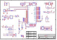
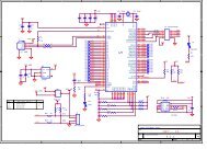
6<strong>SUB</strong>-<strong>20</strong><strong>SUB</strong>-<strong>20</strong> Layout2 <strong>SUB</strong>-<strong>20</strong> Layout© <strong>20</strong>13 xdimax.com rev 2.17
7<strong>SUB</strong>-<strong>20</strong><strong>SUB</strong>-<strong>20</strong> Layout2.1 GPIO HeaderHeader GPIO Alternative Function NotesPin1 GPIO8 I2C SCL Pulled up 1.5KOhm DB9.82 GPIO9 I2C SDA Pulled up 1.5KOhm DB9.63 GPIO10 RS232 RXD_TTL For Configurations with RS232 or RS4854 GPIO11 RS232 TXD_TTL5 GPIO126 GPIO137 GPIO14 MDC8 GPIO15 MDIO9 GPIO24 PWM_0, SCLx0, MISOx0¹10 GPIO25 PWM_1, SDAx0, MOSIx0¹11 GPIO26 PWM_2, SCLx1, SCKx0¹12 GPIO27 PWM_3, SDAx1, SSx0¹13 GPIO28 PWM_4, SCLx2, MISOx1¹, UARTx0_RX¹14 GPIO29 PWM_5, SDAx2, MOSIx1¹, UARTx0_TX¹15 GPIO30 PWM_6, SCLx3, SCKx1¹, UARTx1_RX¹16 GPIO31 PWM_7, SDAx3, SSx1¹, UARTx1_TX¹17 GPIO0 LCD_D0 For Configurations with LCD18 GPIO1 LCD_D119 GPIO2 LCD_D2<strong>20</strong> GPIO3 LCD_D321 GPIO4 IR_TX For Configurations with IR22 GPIO523 GPIO6 LCD_En For Configurations with LCD24 GPIO7 LCD_RS25 GPIO23 ADC726 GPIO22 ADC627 GPIO21 ADC528 GPIO<strong>20</strong> ADC429 GPIO19 ADC330 GPIO18 ADC231 GPIO17 ADC132 GPIO16 ADC033 VCC34 GND¹ - Under development© <strong>20</strong>13 xdimax.com rev 2.17
8<strong>SUB</strong>-<strong>20</strong><strong>SUB</strong>-<strong>20</strong> Layout2.2 SPI HeaderHeader Pin SPI Function Fast GPIOB MDIO1 NotesPWM1 MOSI - Master Out Slave In GPIOB1 MDC1 Optional Level Converter*2 SS1 GPIOB0 GPIO Voltage**3 MISO - Master In Slave Out GPIOB3 Optional Level Converter*4 SS2 FPWM_0 GPIOB2 GPIO Voltage**5 SS0 GPIOB5 Output,Optional LevelConverter*6 SS3 FPWM_1 GPIOB4 GPIO Voltage**7 SCK - Master Clock GPIOB7 MDIO1 Optional Level Converter*8 SS4 FPWM_2 GPIOB6 GPIO Voltage**9 SPI_EXT_PWR - External SPIEXT_PWRPower10 GND GNDLevel Converter* - Adjustable operating voltage in configurations with Level Converters (see Jumpers and OrderingInformation).GPIO Voltage** - Operates at the same voltage as GPIO according to <strong>SUB</strong>-<strong>20</strong> configuration (see Ordering Information).2.3 DB9 ConnectorPin Function Configuration1 SPI SS02 I2C_EXT_PWRRS232 PC_RXSerial23 SPI_EXT_PWR Lxxx© <strong>20</strong>13 xdimax.com rev 2.17
9<strong>SUB</strong>-<strong>20</strong><strong>SUB</strong>-<strong>20</strong> LayoutRS232 PC_TX4 SPI SCK5 GND6 I2C SDA7 SPI MISO8 I2C SCL9 SPI MOSISerial22.4 RS485 ConnectorRS485 Connector is installed only in Serial4 configuration.PinFunctionA inverting or '-' pinB non-inverting or '+' pin2.5 Jumpers, SW1,SW2© <strong>20</strong>13 xdimax.com rev 2.17
10<strong>SUB</strong>-<strong>20</strong><strong>SUB</strong>-<strong>20</strong> LayoutJP1JP2JP3JP4JP5JP6J7BOOT,SW1I2C Pull-ups Voltage when JP2 1-2closedI2C Pull-ups VoltageSCL Pull-upSDA Pull-upSPI Voltage when JP6 1-2 closedSPI VoltageGPIO VoltageForce Bootloader on Power Reset1-2 3.3V2-35V Should not be used with 3.3Vconfigurations1-2 Internal2-3External Can not be used in Serial configurationsDB9.21-2 On2-3 Off1-2 On2-3 Off1-2 3.3V2-3 5V1-2 InternalExternal J6.9 Only for Lxxx configurations.2-3 or DB9.3 DB9.3 Can not be used as SPI Voltage inSerial configurationsleft 5Vrigth 3.3VClosedorPressedSW2 Force Monitor on Power Reset Pressed Only for Serial2 configurationsFor additional information about <strong>SUB</strong>-<strong>20</strong> configurations please see Ordering Information.2.6 Power DistributionThe diagram below shows <strong>SUB</strong>-<strong>20</strong> power distribution and voltage levels.© <strong>20</strong>13 xdimax.com rev 2.17
11<strong>SUB</strong>-<strong>20</strong><strong>SUB</strong>-<strong>20</strong> LayoutCPU and GPIO VoltageCPU and GPIO voltage is defined by J7. It can be 5V from the USB or 3.3V from the internal regulator. Incustomized <strong>SUB</strong>-<strong>20</strong> models 3.3V regulator can be exchanged with 2.7V .. 5V regulator.It is possible to source up to 70mA from GPIO33 to power external target.I2C VoltageI2C voltage is defined by I2C pull-ups voltage. If pull-ups are enabled with JP3, JP4 I2C voltage is controlled byJP2. It can be internal 5V or 3.3V or external taken from DB9.2. External I2C voltage is not available in <strong>SUB</strong>-<strong>20</strong>-R25 (Serial2) model.SPI/MDIO1 VoltageSPI Level Converter and RN1 resistors network are mutually exclusive. SPI Level Converter is available in <strong>SUB</strong>-<strong>20</strong>-Lxxx models.· If SPI Level Converter installed SPI/MDIO1 voltage is defined by JP5 and JP6. It can be 5V or 3.3V if JP6 isconfigured for internal voltage or externally referenced if JP6 is configured for external voltage. External© <strong>20</strong>13 xdimax.com rev 2.17
12<strong>SUB</strong>-<strong>20</strong><strong>SUB</strong>-<strong>20</strong> Layoutvoltage can be taken from SPI.9 or DB9.3 (in non Serial2 model).External voltage reference can be in range1.6V .. 5V for <strong>SUB</strong>-<strong>20</strong>-Lxxx models or 1.2V .. 3.3V for <strong>SUB</strong>-<strong>20</strong>-Lxxx-1.2 models. Models with SPI LevelConverter can not be used in SPI Slave mode.· If SPI Level converter is not installed RN1 is used to rout SPI/MDIO1 signals to SPI header and DB9connector. SPI/MDIO1 voltage in this case is defined by CPU Voltage.© <strong>20</strong>13 xdimax.com rev 2.17
13<strong>SUB</strong>-<strong>20</strong><strong>SUB</strong>-<strong>20</strong> API3 <strong>SUB</strong>-<strong>20</strong> APIAPI Functions Listsub_find_devicessub_opensub_get_serial_numbersub_get_product_idsub_get_versionsub_eep_readsub_eep_writesub_i2c_freqsub_i2c_configsub_i2c_startsub_i2c_stopsub_i2c_scansub_i2c_readsub_i2c_writesub_bb_i2c_configsub_bb_i2c_scansub_bb_i2c_readsub_bb_i2c_writesub_spi_configsub_spi_transfersub_gpio_configsub_gpio_readsub_gpio_writesub_gpiob_configsub_gpiob_readsub_gpiob_writesub_edge_configsub_edge_readsub_fpwm_configsub_fpwm_setsub_adc_configsub_adc_readsub_adc_singlesub_lcd_writesub_rs_set_configsub_rs_get_configsub_rs_timingsub_rs_xfersub_fifo_configsub_fifo_readsub_fifo_write© <strong>20</strong>13 xdimax.com rev 2.17
14<strong>SUB</strong>-<strong>20</strong><strong>SUB</strong>-<strong>20</strong> API3.1 Device InitializationFunctionssub_find_devicessub_opensub_get_serial_numbersub_get_product_id3.1.1 sub_find_devicesSynopsissub_device sub_find_devices( sub_device first )Function scans USB devices currently connected to the host looking for <strong>SUB</strong>-<strong>20</strong> device(s). If parameter first isNULL function will initiate new search, otherwise it will continue to search from the place it finished during lastcall.Return valueFunction returns next found <strong>SUB</strong>-<strong>20</strong> device descriptor or NULL if no more devices were found. Returned valuecan be used as parameter for sub_open. Device descriptor is not a device handle required by API calls. Handleis returned by sub_open.Examplesub_device dev=0;while( dev = sub_find_devices(dev) ){/* Check device serial number */}3.1.2 sub_openSynopsissub_handle sub_open( sub_device dev )Open <strong>SUB</strong>-<strong>20</strong> device. If parameter dev is NULL function will try to open first available <strong>SUB</strong>-<strong>20</strong> device. In thiscase it will call internally sub_find_devices(0). Otherwise function will try to open <strong>SUB</strong>-<strong>20</strong> device referenced bydev. If your application intended to work with single <strong>SUB</strong>-<strong>20</strong> device you can always call sub_open with dev=NULL.Return valueOn success function returns non zero handler that should be used in all subsequent calls to <strong>SUB</strong>-<strong>20</strong> APIfunctions. In case of error function returns NULL and set sub_errnoExamplehandle = sub_open( 0 );if( !handle ){© <strong>20</strong>13 xdimax.com rev 2.17
15<strong>SUB</strong>-<strong>20</strong><strong>SUB</strong>-<strong>20</strong> API}printf("sub_open: %s\n", sub_strerror(sub_errno));return -1;3.1.3 sub_get_serial_numberSynopsisint sub_get_serial_number( sub_handle hndl, char *buf, int sz)Get serial number string descriptorParameters· *buf - buffer to store descriptor· sz - buffer sizeReturn valueOn success function returns string descriptor size. Otherwise negative number.Exampleif( sub_get_serial_number(hndl, buf, sizeof(buf)) >= 0 )printf( "Serial Number : %s\n", buf );else{/* Error */}3.1.4 sub_get_product_idSynopsisint sub_get_product_id( sub_handle hndl, char *buf, int sz);Get product ID string descriptorParameters· *buf - buffer to store descriptor· sz - buffer sizeReturn valueOn success function returns string descriptor size. Otherwise negative number.Exampleif( sub_get_product_id(hndl, buf, sizeof(buf)) >= 0 )printf( "Product ID : %s\n", buf );else{/* Error */}3.1.5 sub_get_versionSynopsisconst struct sub_version* sub_get_version( sub_handle hndl );© <strong>20</strong>13 xdimax.com rev 2.17
16<strong>SUB</strong>-<strong>20</strong><strong>SUB</strong>-<strong>20</strong> APIGet version of shared (DLL) or static library, driver, <strong>SUB</strong>-<strong>20</strong> device and bootloader.Return valueFunction fills internal structure with gathered versions and returns pointer to this structure.Exampleconst struct sub_version* sub_ver;sub_ver = sub_get_version( hndl );3.1.6 sub_resetSynopsisint sub_reset( sub_handle hndl );Reset <strong>SUB</strong>-<strong>20</strong> device.Return valueOn success function returns 0. Otherwise error code.3.2 Internal EEPROM FunctionsBeginning from the firmware version 0.3.4 and library version 0.1.12.26, <strong>SUB</strong>-<strong>20</strong> provides access to it's internalEEPROM (non volatile memory). EEPROM memory array size is 1KB, endurance: 100,000 Write/Erase Cycles.EEPROM Memory array can be freely used by application without any format or interdependency restrictions.Access to EEPROM is gained by two simple functions:sub_eep_readsub_eep_write3.2.1 sub_eep_readSynopsisint sub_eep_read( sub_handle hndl, int addr, char* buf, int sz )Read sz bytes from internal EEPROM starting from address addr. Read data will be stored in buf.Parameters· addr - read start address· buf - buffer to store read data· sz - read size, max 64 bytes.Return valueOn success function returns 0. Otherwise error code.3.2.2 sub_eep_writeSynopsisint sub_eep_write( sub_handle hndl, int addr, char* buf, int sz )Write sz bytes into internal EEPROM starting from address addr. Write data is taken from buf.© <strong>20</strong>13 xdimax.com rev 2.17
17<strong>SUB</strong>-<strong>20</strong><strong>SUB</strong>-<strong>20</strong> APIParameters· addr - write start address· buf - buffer for data to be written· sz - write size, max 64 bytes.Return valueOn success function returns 0. Otherwise error code.3.3 I2C functionsSlave Address ConventionSlave address parameter referenced in I2C related functions is 7 bit number representing I2C slave deviceaddress without R/W bit. For example with slave address parameter equal 0x50 slave address stage of the I2Ctransaction will look like:Acknowledge PollingI2C EEPROM slave devices may enter internal memory write cycle. Once the internally-timed write cycle hasstarted EEPROM inputs are disabled, acknowledge polling can be initiated. This involves sending a startcondition followed by the device slave address and R/W bit. Only if the internal write cycle has completed will theEEPROM respond with an ACK, allowing the read or write sequence to continue. Acknowledge polling should beperformed on application level. <strong>SUB</strong>-<strong>20</strong> knows nothing about nature of I2C slave device it is connected to.EEPROM Page WriteI2C EEPROMs are usually capable of no more then 64-byte page writes. The internal EEPROM data addresslower 6 bits are internally incremented following the receipt of each data byte. The higher data address bits arenot incremented, retaining the memory page row location. When the data address, internally generated, reachesthe page boundary, the following byte is placed at the beginning of the same page. If more than 64 data bytesare transmitted to the EEPROM, the data address will “roll over” and previous data will be overwritten. Theaddress “roll over” during write is from the last byte of the current page to the first byte of the same page.High Speed SupportBeginning from FW version 0.3.2 and library version 0.1.12.24, <strong>SUB</strong>-<strong>20</strong> provides High Speed (HS) I2C Mastercapabilities compliant to "I2C Bus Specification Rev 3.0". HS I2C Master functionality is available viasub_i2c_hs_rw API call. Timing characteristics can be found here HS I2C Master AC CharacteristicsSlave Mode<strong>SUB</strong>-<strong>20</strong> can work in both I2C master and I2C slave modes. Detailed description of I2C slave mode can be foundhere: <strong>SUB</strong>-<strong>20</strong> as I2C Slave.Functions© <strong>20</strong>13 xdimax.com rev 2.17
18<strong>SUB</strong>-<strong>20</strong><strong>SUB</strong>-<strong>20</strong> APIsub_i2c_freqsub_i2c_configsub_i2c_startsub_i2c_stopsub_i2c_readsub_i2c_writesub_i2c_hs_rw3.3.1 sub_i2c_freqSynopsisint sub_i2c_freq( sub_handle hndl, int* freq )Set and get <strong>SUB</strong>-<strong>20</strong> I2C master clock frequency. If *freq is non zero I2C clock frequency will be set to valueequal or close to *freq. <strong>SUB</strong>-<strong>20</strong> has I2C frequency generator that can generate clock frequencies in range form444,444 KHz down to 489 Hz. Function will calculate close possible frequency from the available range. Iffunction succeed *freq will reflect the resulting I2C clock frequency. Some of available I2C clock frequencies arelisted below444444 Hz (Maximal)421052 Hz400000 Hz...100000 Hz...491 Hz489 Hz (Minimal)Parameters· *freq - Desired frequency or zero. On return will be filled with resulting frequencyReturn valueOn success function returns 0. Otherwise error code.3.3.2 sub_i2c_configSynopsisint sub_i2c_config( sub_handle hndl, int sa, int flags )Configure <strong>SUB</strong>-<strong>20</strong> I2C module.Parameters· sa - slave address for <strong>SUB</strong>-<strong>20</strong> in I2C slave mode. See I2C Slave Address Convention and I2C Slave· flags - set of below flagsI2C_GCEEnable general call address (0x00) detection in I2C slave modeI2C_DISABLE Disable I2C module. (Any following I2C transaction will enable I2C module) .I2C_DISABLE is required to get full control over GPIO8,GPIO9 I/Os. WhileI2C module is enabled GPIO8,GPIO9 can only be used as inputs.Return ValueOn success function returns 0. Otherwise error code.© <strong>20</strong>13 xdimax.com rev 2.17
19<strong>SUB</strong>-<strong>20</strong><strong>SUB</strong>-<strong>20</strong> API3.3.3 sub_i2c_startSynopsisint sub_i2c_start( sub_handle hndl )Generate I2C start condition.Return valueOn success function returns 0. Otherwise error code.See alsoError Codes, I2C Status3.3.4 sub_i2c_stopSynopsisint sub_i2c_stop( sub_handle hndl )Generate I2C stop condition.Return valueOn success function returns 0. Otherwise error code.See alsoError Codes, I2C Status3.3.5 sub_i2c_scanSynopsisint sub_i2c_scan( sub_handle hndl, int* slave_cnt, char* slave_buf )Scan I2C bus looking for connected slave devices.Parameters· *slave_cnt - Buffer to store number of found slave devices· slave_buf - Buffer to store found slave device addressesReturn valueOn success function returns 0. Otherwise error code.See alsoError Codes, I2C Status3.3.6 sub_i2c_readSynopsisint sub_i2c_read( sub_handle hndl, int sa, int ma, int ma_sz,char* buf, int sz )Perform complete I2C master read transaction with optional memory address write. Transaction will have© <strong>20</strong>13 xdimax.com rev 2.17
<strong>20</strong><strong>SUB</strong>-<strong>20</strong><strong>SUB</strong>-<strong>20</strong> APIfollowing format:If ma_sz is zero "Memory Address Write" stage will be skipped.Function has no limitation of the read data size - sz parameter. However internal organization of the I2C slavedevice being read should be considered.Parameters· sa - Slave Address· ma - Memory Address. Will be shifted out in "Memory Address Write" stage MSB first· ma_sz - Memory Address size bytes· buf - Buffer to store read data· sz - Read data size bytes.Return valueOn success function returns 0. Otherwise error code.See alsoError Codes, I2C Status3.3.7 sub_i2c_writeSynopsisint sub_i2c_write( sub_handle hndl, int sa, int ma, int ma_sz,char* buf, int sz )Perform complete I2C master write transaction with optional memory address write. Transaction will havefollowing format:If ma_sz is zero "Memory Address Write" stage will be skipped.Function has no limitation of the write data size - sz parameter. However internal organization of the I2C slavedevice being written should be considered especially Acknowledge Polling and EEPROM Page Write.Parameters© <strong>20</strong>13 xdimax.com rev 2.17
21<strong>SUB</strong>-<strong>20</strong><strong>SUB</strong>-<strong>20</strong> API· sa - Slave Address· ma - Memory Address. Will be shifted out in "Memory Address Write" stage MSB first· ma_sz - Memory Address size bytes· buf - Buffer for data to be written· sz - Write data size bytesReturn valueOn success function returns 0. Otherwise error code.See alsoError Codes, I2C Status3.3.8 sub_i2c_hs_rwSynopsisint sub_i2c_hs_rw( sub_handle hndl, int mcode, int count,struct sub_i2c_hs_xfer* px );Perform High Speed (HS) I2C Master read/write transaction(s) with prior master code transmit according toI2C-bus specification. The whole session has the following format:At the beginning of the session both master and slave are in Fast Speed or Standard I2C mode. Master issuesSTART condition and transmits Master Code 00001xxx, where xxx is under SW control via mcode parameter.(Master Code 00001000 should not be used as it is reserved by I2C-bus specification for future extensions).Master Code will not be acknowledged - NAK will be generated. At the end of NAK I2C-bus is in HS mode. Nowmaster can perform HS read/write transactions by issuing REPEATED START condition followed by SlaveAddress with R/W bit and data byte(s) being read/written according to R/W bit. To exit HS mode master issuesSTOP condition. A number of HS transactions can be performed within single HS mode session (it isrecommended by I2C-bus specification).Parameters· mcode - Master Code lower 3 bits· count - number of HS mode read/write transactions to perform· px - pointer to array of count transaction descriptors of type struct sub_i2c_hs_xferstruct sub_i2c_hs_xfer{int sa;int r_w;int sz;int act_sz;char data[64];int status;© <strong>20</strong>13 xdimax.com rev 2.17
22<strong>SUB</strong>-<strong>20</strong><strong>SUB</strong>-<strong>20</strong> API};where:· sa - Slave Address· r_w - 0-write, 1-read· sz - size in bytes of data to read/write· act_sz - actual read/write size. This parameter will be filled by function· data - 64 bytes data buffer. For read transaction function will attempt to read sz bytes into buffer, for writetransaction function will attempt to write sz bytes from buffer. Maximal transaction size is 64 bytes· status - I2C transaction result (see I2C Status).Return valueOn success function returns 0. Otherwise error code. The "I2C Error" return value means that there was a failureat the master code transmit stage. Results of the HS transactions are reported in status field of thecorresponding transaction descriptor.Example/** Master Code 00001001* Write 4 bytes to slave 0x44* Write 2 bytes to slave 0x50* Read 8 bytes from slave 0x44*/struct sub_i2c_hs_xfer xfer[3] ={{ 0x44, 0, 4, 0, "\x10\x11\x12\x13", 0 },{ 0x50, 0, 2, 0, "\x<strong>20</strong>\x30", 0 },{ 0x44, 1, 8, 0, "", 0 }};rc = sub_i2c_hs_rw( hndl, 0x01, 3, xfer, stat );3.3.9 I2C StatusThe status of last I2C operation successful or not successful is stored in sub_i2c_status global variable definedin libsub.h asextern int sub_i2c_status;Following statuses are available:0x00 No errors0x08 START condition transmitted0x10 Repeated START condition transmitted0x18 SLA+W transmitted; ACK received0x<strong>20</strong> SLA+W transmitted; NAK received0x28 Data byte transmitted; ACK received0x30 Data byte transmitted; NAK received0x38 Arbitration lost in SLA; or NAK received0x40 SLA+R transmitted; ACK received0x48 SLA+R transmitted; NAK received0x50 Data received; ACK has been returned0x58 Data received; NAK has been returned0xE0 Arbitration lost0xE1 Arbitration lost in START0xE2 Arbitration lost in STOP0xE3 Arbitration lost in read ACK0xE4 Arbitration lost in read NAK0xE5 Arbitration lost in write0xF8 Unknown error© <strong>20</strong>13 xdimax.com rev 2.17
23<strong>SUB</strong>-<strong>20</strong><strong>SUB</strong>-<strong>20</strong> API0xFFIllegal START or STOP condition3.4 Bit-bang I2C MastersBeginning from the FW version 0.2.6 and library version 0.1.12.16, <strong>SUB</strong>-<strong>20</strong> provides additional four independentI2C master channels on GPIO24..31 compatible with I2C specification 3.0.Header Pin GPIO Alternative I2C Master Function9 GPIO24 SCLx010 GPIO25 SDAx011 GPIO26 SCLx112 GPIO27 SDAx113 GPIO28 SCLx214 GPIO29 SDAx215 GPIO30 SCLx316 GPIO31 SDAx3Each channel can operate in Fast Plus (1000KHz), Fast (400KHz) and Standard (100KHz) modes. In Fast andStandard modes I2C masters support clock stretching.SDAx, SCLx Pull-upsConsidering the fact that bit-bang I2C channels share the GPIO pins with other <strong>SUB</strong>-<strong>20</strong> modules, there are nointernal (mounted on <strong>SUB</strong>-<strong>20</strong> board) pull-ups on these channels. Pull-ups must be provided on target board.Clock StretchingIn Fast and Standard modes bit-bang I2C masters support clock stretching. Clock stretching pauses atransaction by holding the SCL line LOW. The transaction cannot continue until the line is released HIGH again.Slaves can hold the SCL line LOW to force themaster into a wait state until the slave is ready.Functionssub_bb_i2c_configsub_bb_i2c_scansub_bb_i2c_readsub_bb_i2c_write3.4.1 sub_bb_i2c_configSynopsisint sub_bb_i2c_config( sub_handle hndl, int mode, int stretch_ms )Configure <strong>SUB</strong>-<strong>20</strong> Bit-bang I2C Masters module. Configuration is common for all Bit-bang I2C channels.Parameters· mode - Bit-bang I2C Master mode. One of the following flags:BB_I2C_FAST_PFast Plus mode 1000KHzBB_I2C_FASTFast mode 400KHzBB_I2C_STDStandard mode 100KHz· stretch_ms - Clock stretching timeout up to 4194ms. Clock stretching feature is available in Fast and Standardmodes. If SCL line is hold LOW by I2C slave device longer than stretch_ms timeout, Bit-bang I2C functionwill fail and I2C Status will be set to 0xE0.© <strong>20</strong>13 xdimax.com rev 2.17
24<strong>SUB</strong>-<strong>20</strong><strong>SUB</strong>-<strong>20</strong> APIReturn ValueOn success function returns 0. Otherwise error code.CompatibilityFW versionLibrary version0.2.6 or grater0.1.12.16 or grater3.4.2 sub_bb_i2c_scanSynopsisint sub_bb_i2c_scan( sub_handle hndl, int channel, int* slave_cnt,char* slave_buf )Scan I2C bus looking for connected slave devices.Parameters· channel - Bit-bang I2C Master channel 0..3· *slave_cnt - Buffer to store number of found slave devices· slave_buf - Buffer to store found slave device addressesReturn valueOn success function returns 0. Otherwise error code.See alsoError Codes, I2C StatusCompatibilityFW versionLibrary version0.2.6 or grater0.1.12.16 or grater3.4.3 sub_bb_i2c_readSynopsisint sub_bb_i2c_read( sub_handle hndl, int channel, int sa, int ma, int ma_sz,char* buf, int sz )Perform complete I2C master read transaction with optional memory address write. Transaction will havefollowing format:If ma_sz is zero "Memory Address Write" stage will be skipped.Function has no limitation of the read data size - sz parameter. However internal organization of the I2C slavedevice being read should be considered.© <strong>20</strong>13 xdimax.com rev 2.17
25<strong>SUB</strong>-<strong>20</strong><strong>SUB</strong>-<strong>20</strong> APIParameters· channel - Bit-bang I2C Master channel 0..3· sa - Slave Address· ma - Memory Address. Will be shifted out in "Memory Address Write" stage MSB first· ma_sz - Memory Address size bytes· buf - Buffer to store read data· sz - Read data size bytes.Return valueOn success function returns 0. Otherwise error code.See alsoError Codes, I2C StatusCompatibilityFW versionLibrary version0.2.6 or grater0.1.12.16 or grater3.4.4 sub_bb_i2c_writeSynopsisint sub_bb_i2c_write( sub_handle hndl, int channel, int sa, int ma, int ma_sz,char* buf, int sz )Perform complete I2C master write transaction with optional memory address write. Transaction will havefollowing format:If ma_sz is zero "Memory Address Write" stage will be skipped.Function has no limitation of the write data size - sz parameter. However internal organization of the I2C slavedevice being written should be considered especially Acknowledge Polling and EEPROM Page Write.Parameters· channel - Bit-bang I2C Master channel 0..3· sa - Slave Address· ma - Memory Address. Will be shifted out in "Memory Address Write" stage MSB first· ma_sz - Memory Address size bytes· buf - Buffer for data to be written· sz - Write data size bytesReturn valueOn success function returns 0. Otherwise error code.See also© <strong>20</strong>13 xdimax.com rev 2.17
26<strong>SUB</strong>-<strong>20</strong><strong>SUB</strong>-<strong>20</strong> APIError Codes, I2C StatusCompatibilityFW versionLibrary version0.2.6 or grater0.1.12.16 or grater3.5 SPI FunctionsSPI Pins ConfigurationAfter SPI is enabled <strong>SUB</strong>-<strong>20</strong> SPI module will take control over SPI pins.Pin Function Master mode Slave mode DisabledSCK SPI Master Clock Output InputMOSI Master Out Slave In Output InputMISO Master In Slave Out Input Output**SS0 Slave Select 0 Output Hi(Configurable bysub_spi_transfer)InputHiZSS1SS2SS3SS4Slave Select 1..4*If SPI is disabled all SPI pins are in HiZ.** In SPI slave mode MISO is output only when SS0 is lowHiZ(Configurable bysub_spi_transfer)Not in useSPI SCK Polarity and Phase explanationsSPI Transfer format with SPI_SMPL_SETUPSPI_CPOL_RISESPI_CPOL_FALLSampleMOSI PinMISO Pin© <strong>20</strong>13 xdimax.com rev 2.17
27<strong>SUB</strong>-<strong>20</strong><strong>SUB</strong>-<strong>20</strong> APISPI Transfer format with SPI_SETUP_SMPLSPI_CPOL_RISESPI_CPOL_FALLSampleMOSI PinMISO PinFunctionssub_spi_configsub_spi_transfersub_spi_transfer_esssub_sdio_transfer3.5.1 sub_spi_configSynopsisint sub_spi_config( sub_handle hndl, int cfg_set, int* cfg_get )Configure <strong>SUB</strong>-<strong>20</strong> SPI module or read current configuration. If *cfg_get is NULL function will configure SPIaccording to the cfg_set parameter. Otherwise it will read current SPI configuration into *cfg_getParameters· cfg_set - Desired SPI configuration. This parameter is effective only if *cfg_get is NULL. cfg_set should beassembled as a combination of below flagsSPI_ENABLESPI_SLAVESPI_CPOL_RISESPI_CPOL_FALLSPI_SMPL_SETUPSPI_SETUP_SMPLEnable <strong>SUB</strong>-<strong>20</strong> SPI module.SPI module is in Slave mode. sub_spi_transfer can work only when SPI module is inMaster modeSCK is low when idle. See SPI Polarity and Phase explanationsSCK is high when idle. See SPI Polarity and Phase explanationsSample data on leading SCK edge, setup on trailing. See SPI Polarity and PhaseSetup data on leading SCK edge, sample on trailing. See SPI Polarity and PhaseBelow flags are relevant only for SPI master mode (SPI_SLAVE not set)SPI_LSB_FIRSTSPI_MSB_FIRSTTransmit LSB firstTransmit MSB first© <strong>20</strong>13 xdimax.com rev 2.17
28<strong>SUB</strong>-<strong>20</strong><strong>SUB</strong>-<strong>20</strong> APISPI_CLK_8MHZSPI_CLK_4MHZSPI_CLK_2MHZSPI_CLK_1MHZSPI_CLK_500KHZSPI_CLK_250KHZSPI_CLK_125KHZSPI SCK frequency 8 MHzSPI SCK frequency 4 MHzSPI SCK frequency 2 MHzSPI SCK frequency 1 MHzSPI SCK frequency 500 KHzSPI SCK frequency 250 KHzSPI SCK frequency 125 KHzBeginning from FW version 0.3.3 and library version 0.1.12.25 lower SPI frequencies (down to 4KHz) aresupported for SPI Master transfer with sub_spi_transfer function. Special SPI_CLK_HZ(FHZ) macro defined inlibsub.h, where FHZ parameter denotes SPI frequency in Hz. Supported frequencies range is 100.000Hz ..4000Hz. Exact frequency may differ from requested due to integer rounding in division.SPI_CLK_HZ(FHZ)SPI SCK frequency 100.000Hz .. 4000Hz· *cfg_get - Pointer to store current configuration read from <strong>SUB</strong>-<strong>20</strong> device or NULLReturn valueOn success function returns 0. Otherwise error code.Example/* Read current SPI configuration */sub_spi_config( hndl, 0, &spi_config );/* Configure SPI */sub_spi_config( hndl,SPI_ENABLE|SPI_CPOL_RISE|SPI_SMPL_SETUP|SPI_MSB_FIRST|SPI_CLK_4MHZ, 0 );/* Disable SPI */sub_spi_config( hndl, 0, 0 );CompatibilitySPI_CLK_HZ(FHZ)FW versionLibrary version0.3.3 or grater0.1.12.25 or grater3.5.2 sub_spi_transferSynopsisint sub_spi_transfer( sub_handle hndl, char* out_buf, char* in_buf,int sz, int ss_config )Perform SPI master transaction. Depending on out_buf and in_buf parameters transaction can be either read (out_buf==0), write (in_buf==0) or read-write ( both in_buf and out_buf are non zero).Parameters· out_buf - Output data buffer or NULL. If NULL there will be no write transaction and MOSI pin will stayunchanged.· in_buf - Input buffer to store read data or NULL. If NULL there will be no read transaction and data on MISOpin will be ignored.· sz - Transaction size· ss_config - Determines selection and operation of SS pin. ss_config value must be created with macroSS_CONF(SS_N,SS_MODE) ,where SS_N is SS pin number and SS_MODE is one of the following flags:© <strong>20</strong>13 xdimax.com rev 2.17
29<strong>SUB</strong>-<strong>20</strong><strong>SUB</strong>-<strong>20</strong> APISS_HSS_HLSS_HHLSS_HHHLSS_HHHHLSS_HISS_LSS_LHSS_LLHSS_LLLHSS_LLLLHSS_LOSS goes high and stays high during and after transactionSS goes high and stays high during first byte transfer, after that it goes lowSS goes high and stays high during first 2 bytes transfer, after that it goes lowSS goes high and stays high during first 3 bytes transfer, after that it goes lowSS goes high and stays high during first 4 bytes transfer, after that it goes lowSS goes high and stays high during entire transfer, after that it goes lowSS goes low and stays low during and after transactionSS goes low and stays low during first byte transfer, after that it goes highSS goes low and stays low during first 2 bytes transfer, after that it goes highSS goes low and stays low during first 3 bytes transfer, after that it goes highSS goes low and stays low during first 4 bytes transfer, after that it goes highSS goes low and stays low during entire transfer, after that it goes highSS_HiZ SS stays in HiZ mode (Except SS0)If ss_config is zero there will be no SS activity (changes).Return valueOn success function returns 0. Otherwise error code.Example/* Write 10 bytes. Use SS0 low */rc = sub_spi_transfer( hndl, out, 0, 10, SS_CONF(0,SS_LO) );/* Transfer 10 bytes out and 10 bytes in. Use SS2 high */rc = sub_spi_transfer( hndl, out, in, 10, SS_CONF(2,SS_HI) );/* Read 10 bytes. No SS */rc = sub_spi_transfer( hndl, 0, in, 10, 0 );3.5.3 sub_spi_transfer_essSynopsisint sub_spi_transfer_ess( sub_handle hndl, char* out_buf, char* in_buf,int sz, char* ess_str )Perform SPI master transaction with Extended Slave Select control (ESS). Depending on out_buf and in_bufparameters transaction can be either read (out_buf==0), write (in_buf==0) or read-write ( both in_buf andout_buf are non zero).Parameters· out_buf - Output data buffer or NULL. If NULL there will be no write transaction and MOSI pin will stayunchanged.· in_buf - Input buffer to store read data or NULL. If NULL there will be no read transaction and data on MISOpin will be ignored.· sz - Transaction size· ess_str - string defining SS selection and activity during SPI transfer. Characters of the ess_str have followingmeaning0 Select SS01 Select SS12 Select SS23 Select SS34 Select SS4H SS High Byte Transfer© <strong>20</strong>13 xdimax.com rev 2.17
30<strong>SUB</strong>-<strong>20</strong><strong>SUB</strong>-<strong>20</strong> APIL SS Low Byte Transfer^ SS High No Byte Transferv SS Low No Byte Transfer- Small delay without SS changes No Byte TransferReturn valueOn success function returns 0. Otherwise error code.Example/* Write 5 bytes with SS0 Low. Make SS0 High to Low pulse after each byte */rc = sub_spi_transfer( hndl, out, 0, 5, "0L^-vL^-vL^-vL^-vL^-v" );/* Transfer 10 bytes with SS High. Use SS1 for first 5 bytes and SS2 for last */rc = sub_spi_transfer( hndl, out, in, 10, "1HHHHHv-2HHHHHv" );/* Read 10 bytes. SS0 High for first 2 bytes and low after that */rc = sub_spi_transfer( hndl, 0, in, 10, "0HHv" );CompatibilityFW versionLibrary version0.2.9 or grater0.1.12.19 or grater3.5.4 sub_sdio_transferSynopsisint sub_sdio_transfer( sub_handle hndl, char* out_buf, char* in_buf,int out_sz, int in_sz, int ss_config )Perform 3-Wire compatible SPI master transaction like one shown below.1. SS changes according to ss_config parameter.2. out_sz bytes are transmitted via MOSI. MOSI will be in output state during transfer.3. MOSI state is changed to HiZ after last bit transmitted. If required SS changes.4. in_sz bytes received from MISO input. MOSI left in HiZ state.5. SS changes according to ss_config parameter© <strong>20</strong>13 xdimax.com rev 2.17
31<strong>SUB</strong>-<strong>20</strong><strong>SUB</strong>-<strong>20</strong> APISPI Clock - SCK phase and polarity can be configured with sub_spi_config.Above implementation of SPI transaction allows using of the <strong>SUB</strong>-<strong>20</strong> as 3-Wire SPI master. In this caseconnection to 3-Wire device should be as following:Parameters· out_buf - Output data buffer.· in_buf - Input buffer to store read data.· out_sz - Number of bytes to transmit in range 0..60.· in_sz - Number of bytes to receive in range 0..60.· ss_config - Determines selection and operation of SS pin. ss_config value must be created with macroSS_CONF(SS_N,SS_MODE) ,where SS_N is SS pin number and SS_MODE is one of the following flags:SS_HLSS_HISS_LHSS_LOSS goes high and stays high during transmit stage, after that it goes lowSS goes high and stays high during entire transaction (transmit and receive), afterthat it goes lowSS goes low and stays low during transmit stage, after that it goes highSS goes low and stays low during entire transaction (transmit and receive), after thatit goes highSS_HiZ SS stays in HiZ mode (Except SS0)If ss_config is zero there will be no SS activity (changes).Return valueOn success function returns 0. Otherwise error code.Example/* Transmit one byte and receive 3 bytes *//* SS1 goes low during transaction */sub_sdio_transfer( hndl, out_buf, in_buf, 1, 3, SS_CONF(1,SS_LO) );CompatibilityFW versionLibrary version0.1.9 or grater0.1.12.11 or grater© <strong>20</strong>13 xdimax.com rev 2.17
32<strong>SUB</strong>-<strong>20</strong><strong>SUB</strong>-<strong>20</strong> API3.6 MDIO FunctionsMDIO is a Management Data Input/Output Interface defined in IEEE 802.3 Clause 22 and extended in Clause45. It is two signal based interface between Station Management (<strong>SUB</strong>-<strong>20</strong> in our case) and a Physical Layerdevice (PHY). Where a PHY, or grouping of PHY's, is an individually manageable entity, known as an MDIOManageable Device (MMD).Signals· MDC - management data clock. MDC is sourced by <strong>SUB</strong>-<strong>20</strong> to the PHY as the timing reference for transfer ofinformation on the MDIO signal.· MDIO - management data input/output. MDIO is a bidirectional signal between PHY and the <strong>SUB</strong>-<strong>20</strong> It is usedto transfer control information and status between the PHY and the <strong>SUB</strong>-<strong>20</strong>. Control information is driven bythe <strong>SUB</strong>-<strong>20</strong> synchronously with respect to MDC and is sampled synchronously by the PHY. Status informationis driven by the PHY synchronously with respect to MDC and is sampled synchronously by the <strong>SUB</strong>-<strong>20</strong>.Frame Format<strong>SUB</strong>-<strong>20</strong> supports both MDIO frame formats defined in IEEE 802.3 Clause 22 and Clause 45.· Clause 22 MDIO frame format· Clause 45 MDIO frame formatChannelsBeginning from FW version 0.2.8 and library version 0.1.12.18, additional MDIO1 channel is available on SPIheader ( see SPI Header ). To access MDIO1 channel use sub_mdio_xfer_ex function with channel=1.CFP MSA SupportBeginnig from FW version 0.3.2 and library version 0.1.12.24, <strong>SUB</strong>-<strong>20</strong> supports CFP MSA compatibletransactions at 4MHz MDC frequency. See sub_mdio_xfer_ex.Functionssub_mdio22sub_mdio45sub_mdio_xfer, sub_mdio_xfer_ex© <strong>20</strong>13 xdimax.com rev 2.17
33<strong>SUB</strong>-<strong>20</strong><strong>SUB</strong>-<strong>20</strong> API3.6.1 sub_mdio22Synopsisint sub_mdio22( sub_handle hndl, int op, int phyad, int regad,int data, int* content )Generate IEEE 802.3 Clause 22 MDIO READ or WRITE frame. Frame format is shown here: Clause 22 MDIOframe.Parameters· op - operation code<strong>SUB</strong>_MDIO22_READ<strong>SUB</strong>_MDIO22_WRITEREAD operationWRITE operation· phyad - 5 bit PHY address· regad - 5 bit register address· data - 16 bit data for WRITE operation· *content - 16 bit register content placeholder for READ operationReturn valueOn success function returns 0. Otherwise error code.Example/* Read register 0x12 in PHY 1 */rc = sub_mdio22( hndl, <strong>SUB</strong>_MDIO22_READ, 0x01, 0x12, 0, &content );/* Write register 0x5 in PHY 2 */rc = sub_mdio22( hndl, <strong>SUB</strong>_MDIO22_WRITE, 0x02, 0x05, 0x55AA, 0 );CompatibilityFW versionLibrary version0.2.1 or grater0.1.12.12 or grater3.6.2 sub_mdio45Synopsisint sub_mdio45( sub_handle hndl, int op, int prtad, int devad,int data, int* content )Generate IEEE 802.3 Clause 45 MDIO frame. Frame format is shown here: Clause 45 MDIO frame.Parameters· op - operation code<strong>SUB</strong>_MDIO45_ADDR<strong>SUB</strong>_MDIO45_WRITE<strong>SUB</strong>_MDIO45_PRIA<strong>SUB</strong>_MDIO45_READADDRESS operationWRITE operationPOST-READ-INCREMENT-ADDRESS operationREAD operation· prtad - 5 bit port address· devad - 5 bit device address· data - 16 bit address or data for ADDRESS or WRITE operation© <strong>20</strong>13 xdimax.com rev 2.17
34<strong>SUB</strong>-<strong>20</strong><strong>SUB</strong>-<strong>20</strong> API· *content - 16 bit register content placeholder for READ or POST-READ-INCREMENT-ADDRESS operationReturn valueOn success function returns 0. Otherwise error code.CompatibilityFW versionLibrary version0.2.1 or grater0.1.12.12 or grater3.6.3 sub_mdio_xfer, sub_mdio_xfer_exSynopsisint sub_mdio_xfer( sub_handle hndl, int count, union sub_mdio_frame* mdios )int sub_mdio_xfer_ex( sub_handle hndl, int channel, int count,union sub_mdio_frame* mdios )Generate a sequence of independent MDIO frames. Frames in sequence can be Clause 22 or Clause 45 formatwith different operations and addresses.Parameters· channel - mdio channel (see MDIO Channels ). Optional <strong>SUB</strong>_CFP_MSA flag applied to channel (channel|<strong>SUB</strong>_CFP_MSA) will force <strong>SUB</strong>-<strong>20</strong> to generate CFP MSA compatible transaction(s) at 4MHz MDCfrequency.· count - number of frames to generate (currently up to 15).· *mdios - array of count sub_mdio_frame unionsunion sub_mdio_frame{struct{int op;int phyad;int regad;int data;}clause22;struct{int op;int prtad;int devad;int data;}clause45;};Frame operation is defined by op field value.clause22.op can be<strong>SUB</strong>_MDIO22_READ<strong>SUB</strong>_MDIO22_WRITEclause45.op can be<strong>SUB</strong>_MDIO45_ADDR<strong>SUB</strong>_MDIO45_WRITE<strong>SUB</strong>_MDIO45_PRIAREAD operationWRITE operationADDRESS operationWRITE operationPOST-READ-INCREMENT-ADDRESS operation© <strong>20</strong>13 xdimax.com rev 2.17
35<strong>SUB</strong>-<strong>20</strong><strong>SUB</strong>-<strong>20</strong> API<strong>SUB</strong>_MDIO45_READREAD operationFor READ and POST-READ-INCREMENT-ADDRESS operations clause22.data or clause45.data will be filledwith data read from PHY.Return valueOn success function returns 0. Otherwise error code.Exampleunion sub_mdio_frame mdios[2];mdios[0].clause22.op = <strong>SUB</strong>_MDIO22_READ;mdios[0].clause22.phyad = 0x01;mdios[0].clause22.regad = 0x12;mdios[1].clause45.op = <strong>SUB</strong>_MDIO45_ADDR;mdios[1].clause45.prtad = 0x04;mdios[1].clause45.devad = 0x02;mdios[1].clause45.data = 0x55AA;rc = sub_mdio_xfer( hndl, 2, mdios );Compatibilitysub_mdio_xferFW versionLibrary versionsub_mdio_xfer_exFW versionLibrary version<strong>SUB</strong>_CFP_MSAFW versionLibrary version0.2.1 or grater0.1.12.12 or grater0.2.8 or grater0.1.12.18 or grater0.3.2 or grater0.1.12.24 or grater3.7 GPIO FunctionsGPIO Functional Description<strong>SUB</strong>-<strong>20</strong> GPIO can be in input or output state. GPIO state is defined by configuration bit. In output state GPIO willdrive high or low level depending on output status. In input state GPIO can be pulled high by internal weak pullupresistor.© <strong>20</strong>13 xdimax.com rev 2.17
36<strong>SUB</strong>-<strong>20</strong><strong>SUB</strong>-<strong>20</strong> APIGPIO Pin configurationConfiguration StateOutput Status"0" "1""0" Input state HiZ pull-up"1" Output state LOW HIGHGPIOBGPIOB are located on SPI header (see SPI Header). GPIOB module shares I/O pins with SPI module. If SPI isenabled MISO,MOSI,SCK and SS0 pins are partially controlled by SPI module, although they can be accessedby GPIOB functions with restrictions.Special care should be taken for <strong>SUB</strong>-Lxxx models where SPI Level Converters are installed. In this caseGPIOB pins direction should respect direction of the corresponding Level Converter to prevent shortcircuit on this pins.Functionssub_gpio_configsub_gpio_readsub_gpio_writesub_gpiob_config© <strong>20</strong>13 xdimax.com rev 2.17
37<strong>SUB</strong>-<strong>20</strong><strong>SUB</strong>-<strong>20</strong> APIsub_gpiob_readsub_gpiob_write3.7.1 sub_gpio_configSynopsisint sub_gpio_config( sub_handle hndl, int set, int* get, int mask )Configure GPIO state (direction) as input or output.Parameters· set - Bits 0..31 of set parameter correspond to GPIO0..GPIO31 configuration bits. If GPIOn configuration bit is"1" then GPIOn direction is output, otherwise it is input.· *get - Pointer to store current GPIO configuration read from <strong>SUB</strong>-<strong>20</strong>.· mask - Bit in set parameter will take effect only if corresponding mask bit is "1". With mask=0 function willonly read current GPIO configuration.Return valueOn success function returns 0. Otherwise error code.Example/* gpio0..6 - input, gpio7 - output */rc = sub_gpio_config( hndl, 0x00000080, &config, 0x000000FF );/* read gpio configuration */rc = sub_gpio_config( hndl, 0, &config, 0 );See alsoError Codes3.7.2 sub_gpio_readSynopsisint sub_gpio_read( sub_handle hndl, int* get )Read GPIO input status. Function reads logic value "1"-high, "0"-low directly from GPIO pin.Parameters· *get - Pointer to store received GPIO input status. Bits 0..31 of *get correspond to GPIO0..GPIO31 inputstatuses.Return valueOn success function returns 0. Otherwise error code.See alsoError Codes3.7.3 sub_gpio_writeSynopsisint sub_gpio_write( sub_handle hndl, int set, int* get, int mask )Set GPIO output status. For GPIO in output state function will set output driver to drive "1"-high, "0"-low. For© <strong>20</strong>13 xdimax.com rev 2.17
38<strong>SUB</strong>-<strong>20</strong><strong>SUB</strong>-<strong>20</strong> APIGPIO in input state function will "1"-enable, "0"-disable weak pull-up on corresponding GPIO pin.Parameters· set - Bits 0..31 of set parameter correspond to GPIO0..GPIO31 output statuses.· *get - Pointer to store current GPIO output status read from <strong>SUB</strong>-<strong>20</strong>.· mask - Bit in set parameter will take effect only if corresponding mask bit is "1". With mask=0 function willonly read current GPIO output status.Return valueOn success function returns 0. Otherwise error code.See alsoError Codes3.7.4 sub_gpiob_configSynopsisint sub_gpiob_config( sub_handle hndl, int set, int* get, int mask )Configure GPIOB state (direction) as input or output.Parameters· set - Bits 0..7 of set parameter correspond to GPIOB0..GPIOB7 configuration bits. If GPIOBn configuration bitis "1" then GPIOBn direction is output, otherwise it is input.· *get - Pointer to store current GPIOB configuration read from <strong>SUB</strong>-<strong>20</strong>.· mask - Bit in set parameter will take effect only if corresponding mask bit is "1". With mask=0 function willonly read current GPIOB configuration.Return valueOn success function returns 0. Otherwise error code.See alsoError CodesCompatibilityFW versionLibrary version0.2.7 or grater0.1.12.17 or grater3.7.5 sub_gpiob_readSynopsisint sub_gpiob_read( sub_handle hndl, int* get )Read GPIOB input status. Function reads logic value "1"-high, "0"-low directly from GPIOB pin.Parameters· *get - Pointer to store received GPIOB input status. Bits 0..7 of *get correspond to GPIOB0..GPIOB7 inputstatuses.Return valueOn success function returns 0. Otherwise error code.See alsoError Codes© <strong>20</strong>13 xdimax.com rev 2.17
39<strong>SUB</strong>-<strong>20</strong><strong>SUB</strong>-<strong>20</strong> APICompatibilityFW versionLibrary version0.2.7 or grater0.1.12.17 or grater3.7.6 sub_gpiob_writeSynopsisint sub_gpiob_write( sub_handle hndl, int set, int* get, int mask )Set GPIOB output status. For GPIOB in output state function will set output driver to drive "1"-high, "0"-low. ForGPIO in input state function will "1"-enable, "0"-disable weak pull-up on corresponding GPIOB pin.Parameters· set - Bits 0..7 of set parameter correspond to GPIOB0..GPIOB7 output statuses.· *get - Pointer to store current GPIOB output status read from <strong>SUB</strong>-<strong>20</strong>.· mask - Bit in set parameter will take effect only if corresponding mask bit is "1". With mask=0 function willonly read current GPIOB output status.Return valueOn success function returns 0. Otherwise error code.See alsoError CodesCompatibilityFW versionLibrary version0.2.7 or grater0.1.12.17 or grater3.7.7 Edge DetectorEdge Detector description<strong>SUB</strong>-<strong>20</strong> Edge detector module (EDGE) is capable to detect falling, rising or "any change" edge on the GPIOpins listed below.GPIO Header Pin GPIO Edge Number1 GPIO8 EDG02 GPIO9 EDG13 GPIO10 EDG24 GPIO11 EDG313 GPIO28 EDG414 GPIO29 EDG515 GPIO30 EDG616 GPIO31 EDG7Pulses on EDG7:0 pins wider than the minimum pulse width of 50ns will trigger edge detection. If enabled, theedge detection will trigger even if the corresponding GPIO are configured as outputs.Functionssub_edge_configsub_edge_read© <strong>20</strong>13 xdimax.com rev 2.17
40<strong>SUB</strong>-<strong>20</strong><strong>SUB</strong>-<strong>20</strong> API3.7.7.1 sub_edge_configSynopsisint sub_edge_config( sub_handle hndl, int set, int* get )Configure EDGE module.Parameters· set - set will be used only if get == 0. EDGE lines EDG7..EDG0 are configured by two bits Ex1,Ex0 in setwhere x is 7..0. set bits have following interpretation:MSB31..16 15 14 13 12 11 10 09 08 07 06 05 04 03 02 01 00- EDG7 EDG6 EDG5 EDG4 EDG3 EDG2 EDG1 EDG0- E71 E70 E61 E60 E51 E50 E41 E40 E31 E30 E21 E<strong>20</strong> E11 E10 E01 E00Ex1 Ex0 Edge Detection0 0 No0 1 Any change1 0 Falling edge1 1 Rising edge· *get - Pointer to store current edge configuration read from <strong>SUB</strong>-<strong>20</strong>. If get is not zero function will read edgeconfiguration otherwise it will set edge configurationReturn valueOn success function returns 0. Otherwise error code.Examplerc = sub_edge_config( hndl, 0, &edge_config ); /* Read Edge configuration *//* EDG0 = 01B - Any change *//* EDG1 = 01B - Any change *//* EDG2 - 11B - Risinge edge *//* EDG7..EDG3 not detected */rc = sub_edge_config( hndl, 0x0035, 0 ); /* set = 0011.0101B */See alsoError Codes3.7.7.2 sub_edge_readSynopsisint sub_edge_read( sub_handle hndl, int* get, int* edge )Read GPIO input status and EDGE status. For GPIO Function reads logic value "1"-high, "0"-low directly fromGPIO pin. For EDGE function reads "1" - edge detected, "0" - edge not detected.Parameters· *get - Pointer to store received GPIO input status. Bits 0..31 of *get correspond to GPIO0..GPIO31 inputstatuses.· *edge - Pointer to store EDGE status. Bits 0..7 of *edge correspond to EDG0..EDG7.Return valueOn success function returns 0. Otherwise error code.See also© <strong>20</strong>13 xdimax.com rev 2.17
41<strong>SUB</strong>-<strong>20</strong><strong>SUB</strong>-<strong>20</strong> APIError Codes3.7.8 Fast PWMFast PWM outputs are available on SPI header pins 4,6,8 (see SPI Header). Outputs are referenced asFPWM_0, FPWM_1 and FPWM_2. All three outputs share the same PWM generation module in <strong>SUB</strong>-<strong>20</strong> andhave the same PWM frequency but separate duty cycle configuration.Fast PWM frequency range is 8Mhz .. 0.238Hz. Duty cycle precision is 2..16 bits depending on the PWMfrequency.Functionssub_fpwm_configsub_fpwm_set© <strong>20</strong>13 xdimax.com rev 2.17
42<strong>SUB</strong>-<strong>20</strong><strong>SUB</strong>-<strong>20</strong> API3.7.8.1 sub_fpwm_configSynopsisint sub_fpwm_config( sub_handle hndl, double freq_hz, int flags )Configure fast PWM module.Parameters· freq_hz - Desired fast PWM frequency in Hz. Frequency can be in a range 8MHz .. 0.238Hz· flags - Set of configuration flags listed belowFPWM_ENABLEFPWM_EN0FPWM_EN1FPWM_EN2General fast PWM enable. If this flag is not set fast PWM module will bedisabled and FPWM outputs will go to HiZ.Enable FPWM_0 output. Otherwise FPWM_0 will stay low.Enable FPWM_1 output. Otherwise FPWM_1 will stay low.Enable FPWM_2 output. Otherwise FPWM_2 will stay low.Return valueOn success function returns 0. Otherwise error code.Example/*Enable fast PWM module with FPWM_0 and FPWM_2 outputs.PWM frequency 10.6Hz*/sub_fpwm_config( hndl, 10.6, FPWM_ENABLE|FPWM_EN0FPWM_EN2 );See alsosub_fpwm_setError Codes3.7.8.2 sub_fpwm_setSynopsisint sub_fpwm_set( sub_handle hndl, int pwm_n, double duty )Configure specific fast PWM output.Parameters· pwm_n - number of FPWM output to configure. Can be 0,1,2· duty - desired duty cycle % in range 0..100. Can be not integer.Return valueOn success function returns 0. Otherwise error code.Examplesub_fpwm_set( hndl, 0, <strong>20</strong> );sub_fpwm_set( hndl, 1, 30.5 );sub_fpwm_set( hndl, 2, 12.25 );See alsosub_fpwm_configError Codes© <strong>20</strong>13 xdimax.com rev 2.17
43<strong>SUB</strong>-<strong>20</strong><strong>SUB</strong>-<strong>20</strong> API3.7.9 PWMPWM outputs are available on GPIO24..GPIO31 pins (see GPIO Header). Outputs are referenced as PWM_0 ..PWM_7.PWM generation module shown below has configurable source clock, counter limit and separate comparator foreach PWM output.PWM module resolution and limit are configured with sub_pwm_config. Duty cycle of each PWM output can beset with sub_pwm_set.PWM module output signal controls output driver of the corresponding GPIO (see GPIO Functions). To gethigh/low transition of the GPIO pin it should be configured to output state with sub_gpio_config.Otherwise PWM module will enable/disable internal pull-up.Functionssub_fpwm_configsub_pwm_set3.7.9.1 sub_pwm_configSynopsisint sub_pwm_config( sub_handle hndl, int res_us, int limit )Configure PWM module.Parameters© <strong>20</strong>13 xdimax.com rev 2.17
44<strong>SUB</strong>-<strong>20</strong><strong>SUB</strong>-<strong>20</strong> API· res_us - PWM module clock resolution in µs. Resolution range is <strong>20</strong>µs - 16384µs.· limit - PWM module counter limit in range 0-255. If limit is 0 PWM module will be turned off.PWM frequencyResolution and limit define PWM module frequencyFpwm = 1000000/(res_us * limit) HzPWM frequency range isFpwm_min = 1000000/(<strong>20</strong> * 2) = 25000 Hz = 25KHzFpwm_max = 1000000/(16384 * 255) = 0.238 HzReturn valueOn success function returns 0. Otherwise error code.See alsosub_pwm_setError CodesCompatibilityFW versionLibrary version0.1.8 or grater0.1.12.10 or grater3.7.9.2 sub_pwm_setSynopsisint sub_pwm_set( sub_handle hndl, int pwm_n, int duty )Configure specific PWM output.Parameters· pwm_n - number of PWM output to configure. Can be 0..7.· duty - Duty cycle in range 0..255Duty cycle· If duty cycle is 0, PWM output will be constantly low· If duty cycle is grater or equal to the limit set by sub_pwm_config, PWM output will be constantly highEffective duty cycle in percent can be calculated asDUTY% = duty/limit * 100%Duty cycle resolution in bits depends on limit. It can be in range of 1 bit for limit=2 up to 8 bit for limit=255Return valueOn success function returns 0. Otherwise error code.Example/* Set PWM resolution=10ms, limit=100, frequency=1Hz */sub_pwm_config( hndl, 10000, 100 );/* Set PWM_0 pin (GPIO24) to output state */sub_gpio_config( hndl, 0x01000000, &config, 0x01000000 );/* Output 50% duty cycle on PWM_0 pin */© <strong>20</strong>13 xdimax.com rev 2.17
45<strong>SUB</strong>-<strong>20</strong><strong>SUB</strong>-<strong>20</strong> APIsub_pwm_set( hndl, 0, 50 );See alsosub_pwm_configError CodesCompatibilityFW versionLibrary version0.1.8 or grater0.1.12.10 or grater3.8 Analog to Digital Converter - ADC<strong>SUB</strong>-<strong>20</strong> has 8 single ended and a 16 differential analog input combinations with x1 x10 or x<strong>20</strong>0 input gainamplifier. Analog inputs are referenced as ADC0..ADC7 see GPIO Header. The <strong>SUB</strong>-<strong>20</strong> ADC module features a10-bit successive approximation ADC. The ADC contains a Sample and Hold circuit which ensures that the inputvoltage to the ADC is held at a constant level during conversion.Functionssub_adc_configsub_adc_singlesub_adc_read3.8.1 sub_adc_configSynopsisint sub_adc_config( sub_handle hndl, int flags )Configure <strong>SUB</strong>-<strong>20</strong> ADC module.Parameters· flags - set of below flagsADC_ENABLEADC_REF_VCCADC_REF_2_56Enable ADC module. If this flag is not set ADC module will be disabledUse VCC as ADC referenceUse internal 2.56V referenceReturn valueOn success function returns 0. Otherwise error code.3.8.2 sub_adc_singleSee sub_adc_read.3.8.3 sub_adc_readSynopsisint sub_adc_single( sub_handle hndl, int* data, int mux );int sub_adc_read( sub_handle hndl, int* data, int* mux, int reads );Read single or multiple ADC conversion result(s)© <strong>20</strong>13 xdimax.com rev 2.17
46<strong>SUB</strong>-<strong>20</strong><strong>SUB</strong>-<strong>20</strong> APIParameters· data - buffer to store conversion result(s)· mux - ADC input channel multiplexer control code(s). See table below.· reads - number of results to readADC mux codeSingle EndedDifferentialPositiveDifferentialNegativeADC_S0ADC0ADC_S1ADC1ADC_S2ADC2ADC_S3ADC3ADC_S4ADC4N.A.ADC_S5ADC5ADC_S6ADC6ADC_S7ADC7ADC_D10_10XADC1 ADC0 10ADC_D10_<strong>20</strong>0X ADC1 ADC0 <strong>20</strong>0ADC_D32_10X ADC3 ADC2 10ADC_D32_<strong>20</strong>0X ADC3 ADC2 <strong>20</strong>0ADC_D01 ADC0 ADC1ADC_D21 ADC2 ADC1ADC_D31 ADC3 ADC1ADC_D41 ADC4 ADC1N.A.ADC_D51 ADC5 ADC1ADC_D61 ADC6 ADC1ADC_D71 ADC7 ADC1N.A.ADC_D02 ADC0 ADC2ADC_D12 ADC2 ADC2ADC_D32 ADC3 ADC2ADC_D42 ADC4 ADC2ADC_D52 ADC5 ADC2ADC_1_1V Internal 1.1VADC_GNDAnalog GNDN.A.ADC ResultFor single ended conversion:GainFor differential:ADC is a result of conversion. Note that the result of differential conversion is signed and can be negative.Return valueOn success function returns 0. Otherwise error code.Exampleint adc, adc_buf[3], adc_mux[3];© <strong>20</strong>13 xdimax.com rev 2.17
47<strong>SUB</strong>-<strong>20</strong><strong>SUB</strong>-<strong>20</strong> APIsub_adc_single( fd, &adc, ADC_S0 ); /* Read ADC on ADC0 input */adc_mux[0] = ADC_S0;adc_mux[1] = ADC_S2;adc_mux[2] = ADC_S3;sub_adc_read( fd, adc_buf, adc_mux, 3 ); /* Read ADC on ADC0,2,3 inputs */3.9 LCD FunctionsFunctions· sub_lcd_write3.9.1 sub_lcd_writeSynopsisint sub_lcd_write( sub_handle hndl, char* str );This function will work only on <strong>SUB</strong>-<strong>20</strong> configurations with LCD.Characters from *str are written to the LCD beginning from the current LCD position. Special characters andsequences listed below are used to format LCD output and control current position.ANSI C notation Hex value Description Example\f 0x0C Clear LCD and go to first position "\fHello"\r 0x0D Go to first position "\r0123"\n 0x0A Go to next string "\rHello\nWorld"\eXY 0x1B X Y Go to position X,Y "\e00Hello\e01World"Every string written to LCD will be space padded till the end of the string.Parameters· *str - LCD stringReturn valueOn success function returns 0. If LCD is not supported function will return "Feature not supported".Examplesub_lcd_write( hndl,"\fHello\nWorld" );sub_lcd_write( hndl,"\f\e<strong>20</strong>Hello\e21World" );sub_lcd_write( hndl, "\r1\n2" ); 12sub_lcd_write( hndl, "\fT:\nR:");sub_lcd_write( hndl,"\e<strong>20</strong>abc\e21def" );HelloWorldHelloWorldT:abcR:defCompatibility· Required firmware version > 0.0.4© <strong>20</strong>13 xdimax.com rev 2.17
48<strong>SUB</strong>-<strong>20</strong><strong>SUB</strong>-<strong>20</strong> API· Required DLL version > 0.1.12.23.10 RS232 RS485 FunctionsRS232 RS485 Frame formatFunctionssub_rs_set_configsub_rs_get_configsub_rs_timingsub_rx_xfer3.10.1 sub_rs_set_configSynopsisint sub_rs_set_config( sub_handle hndl, int config, int baud)Configure <strong>SUB</strong>-<strong>20</strong> UART (Universal Asynchronous Receiver Transmitter).Parameters· config - UART configuration. Config should be assembled as a combination of the following flagsRS_RX_ENABLERS_TX_ENABLERS_CHAR_5RS_CHAR_6RS_CHAR_7RS_CHAR_8RS_CHAR_9RS_PARITY_NONERS_PARITY_EVENRS_PARITY_ODDRS_STOP_1RS_STOP_2Enable UART receiverEnable UART transmitterData BitsParityStop BitsTo disable UART provide configuration without RS_RX_ENABLE and RS_TX_ENABLE.© <strong>20</strong>13 xdimax.com rev 2.17
49<strong>SUB</strong>-<strong>20</strong><strong>SUB</strong>-<strong>20</strong> API· baud - Desired baudrate. Maximum baudrate is 2Mbps. The actual baudrate may slightly differ from thedesired as actual baudrate is an integer quotient from dividing the 16MHz reference clock.Return valueOn success function returns 0. Otherwise error code.Example/* Set 9660 bps, 8 data bits, no parity, 1 stop bit */sub_rs_set_config( hndl,RS_RX_ENABLE|RS_TX_ENABLE|RS_CHAR_8|RS_PARITY_NONE|RS_STOP_1, 9600 );3.10.2 sub_rs_get_configSynopsisint sub_rs_get_config( sub_handle hndl, int* config, int* baud)Read current <strong>SUB</strong>-<strong>20</strong> UART configuration.Parameters· *config - will be filled with UART configuration see sub_rs_set_config for details· *baud - will be filled with actual UART baudrateReturn valueOn success function returns 0. Otherwise error code.3.10.3 sub_rs_timingSynopsisint sub_rs_timing( sub_handle hndl, int flags, int tx_space_us,int rx_msg_us, int rx_byte_us )Configure UART transfer timing and order of transmit and receive operations. Actual transfer is initiated bysub_rx_xfer function.Parameters· flags - one or none of the below flags:RS_RX_BEFORE_TXRS_RX_AFTER_TXnoneReceive message and after that transmit messageTransmit message and after that receive messageReceive and transmit simultaneously· tx_space_us - delay in µs between subsequent byte transmit· rx_msg_us - message reception timeout in µs· rx_byte_us - byte to byte reception timeout in µsDelay and timeouts precision is ± 64 µs. They should not exceed 4.000.000µs = 4s.Following table explains relation between rx_msg_us and rx_byte_us parametersrx_msg_us=0 rx_byte_us=0 Message reception will last no more then 4srx_msg_us=0 rx_byte_us>0 First byte reception will last no more then 4s. Every next byte shouldbe received in rx_byte_us timerx_msg_us>0 rx_byte_us=0 Message reception will last no more then rx_msg_us time© <strong>20</strong>13 xdimax.com rev 2.17
50<strong>SUB</strong>-<strong>20</strong><strong>SUB</strong>-<strong>20</strong> APIrx_msg_us>0 rx_byte_us>0 First byte reception will last no more then rx_msg_us time. Every nextbyte should be received in rx_byte_us timeReturn valueOn success function returns 0. Otherwise error code.Example/* Request message transmit and after that receipt *//* No space between transmitted bytes *//* Message should be received in 1s */sub_rs_timing( hndl, RS_RX_AFTER_TX, 0, 1000000, 0 );3.10.4 sub_rs_xferSynopsisint sub_rs_xfer( sub_handle hndl, char* tx_buf, int tx_sz,char* rx_buf, int rx_sz )Transmit and/or receive message(s) via UART configured with sub_rs_set_config and in accordance withtransfer timing set with sub_rs_timing.Parameters· tx_buf - buffer with data to be transmitted· tx_sz - number of bytes to transmit (can be 0 if transmit not required)· rx_buf - buffer to store received data· rx_sz - maximal number of bytes to receive (can be 0 if reception is not required)rx_sz and tx_sz should not be grater then 62 bytes.Function will terminate after following conditions fulfilled: tx_sz bytes transmitted and either rx_sz bytes receivedor one of the timeouts occurs (see sub_rs_timing)For 9bit transfer data in tx_buf and rx_buf has following formatbyte 0 byte 1 ... byte n byte n+1bit ..8 LSB bits 7..0 ... bit ..8 LSB bits 7..0Even bytes (0,2,4,....) contain 8'th bit in LSB. Odd bytes (1,3,5,...) contain bits 7..0. Data is shifted out beginningfrom bit 0 (see RS232 RS485 Frame format). Parameters tx_sz and rx_sz should correspond to total number ofbytes in tx_buf and rx_buf.Return valueOn success function returns non negative value that denotes number of received bytes. It can be less thenrx_sz if timeout occurs.Otherwise -1 will be returned and sub_errno will contain error code.Example/* Set timing */sub_rs_timing( hndl, RS_RX_AFTER_TX, 0, 1000000, <strong>20</strong>0000 );/*Transmit 3 bytes and try to receive up to 5 bytesin 1s with <strong>20</strong>0ms byte to byte timeout*/© <strong>20</strong>13 xdimax.com rev 2.17
51<strong>SUB</strong>-<strong>20</strong><strong>SUB</strong>-<strong>20</strong> APIsub_rs_xfer( hndl, "at\r", 3, rx_buf, 5 );CompatibilityFW version9-bit transfer support - 0.2.2 or grater3.11 FIFO, Streaming, Slave ModesFIFO is used for implementation of streaming data transfer and slave modes functionality such as SPI slave, I2Cslave. Below is simplified block diagram of the <strong>SUB</strong>-<strong>20</strong> FIFO module.3.11.1 FIFO Functionssub_fifo_configsub_fifo_readsub_fifo_write© <strong>20</strong>13 xdimax.com rev 2.17
52<strong>SUB</strong>-<strong>20</strong><strong>SUB</strong>-<strong>20</strong> API3.11.1.1 sub_fifo_configSynopsisint sub_fifo_config( sub_handle hndl, int config )Configure FIFO.Parameters· config - set of FIFO configuration flags listed belowFIFO_SELECT_SPIConnect SPI module to FIFOFIFO_SELECT_I2CConnect I2C slave module to FIFOFIFO_SELECT_UART Connect UART to FIFOFIFO_CLEARClear IN and OUT FIFO buffersFIFO_READ_FULLRead only full 64 byte FIFO buffersReturn valueOn success function returns 0. Otherwise error code.CompatibilityFW versionLibrary versionFIFO_CLEAR - 0.1.3 or graterFIFO_SELECT_UART - 0.2.0 or grater0.1.12.10 or grater3.11.1.2 sub_fifo_writeSynopsisint sub_fifo_write( sub_handle hndl, char* buf, int sz, int to_ms )Function attempts to transfer sz bytes from buffer into OUT FIFO in no more then to_ms time.Parameters· buf - source buffer· sz - buffer size· to_ms - timeout in millisecondsReturn ValueOn success a non negative number of actually written bytes is returned. It can be less then or equal to sz. Incase of error negative error code (defined in errno.h) will be returned and if applicable sub_errno will be set tothe corresponding value. Possible error codes are-ENOENT (-2) USB failure-EIO (-5)USB failure-ENOMEM (-12) Memory failure-EINVAL (-22) Invalid parameter-EFBIG (-27) Buffer overflow-ETIMEDOUT (-116) Timeout3.11.1.3 sub_fifo_readSynopsisint sub_fifo_read( sub_handle hndl, char* buf, int sz, int to_ms )Function attempts to read sz bytes from IN FIFO into buffer in no more then to_ms time.Parameters· buf - destination buffer© <strong>20</strong>13 xdimax.com rev 2.17
53<strong>SUB</strong>-<strong>20</strong><strong>SUB</strong>-<strong>20</strong> API· sz - buffer size. Considering internal FIFO structure it is highly recommended to use only 64 divisible szvalues and corresponding buffer size. It will guarantee better performance and no buffer overflow error(-EFBIG).· to_ms - timeout in millisecondsReturn ValueOn success a non negative number of actually read bytes is returned. It can be less then or equal to sz. In caseof error negative error code (defined in errno.h) will be returned and if applicable sub_errno will be set to thecorresponding value. Possible error codes are-ENOENT (-2) USB failure-EIO (-5)USB failure-ENOMEM (-12) Memory failure-EINVAL (-22) Invalid parameter-EFBIG (-27) Buffer overflow. To prevent this error use 64 divisible sz-ETIMEDOUT (-116) TimeoutKnown IssueIf IN FIFO contains exactly 64 or 128 bytes, attempt to read more then 64 or 128 bytes correspondingly withsub_fifo_read will cause to timeout (-116). As a workaround always call sub_fifo_read with sz=64.3.11.2 SPI SlaveConfigurationTo use <strong>SUB</strong>-<strong>20</strong> in SPI slave mode following should be done:· Configure SPI module with sub_spi_config. Make sure to set SPI_SLAVE flag.· Connect SPI module to FIFO with sub_fifo_config. FIFO_SELECT_SPI must be set.· If required, write data to FIFO with sub_fifo_write. This data will be read by external SPI master.· If required, read data from FIFO with sub_fifo_read. This will be data written by external SPI master.ExampleBelow is an example to exchange 12 bytes with SPI master:sub_spi_config( hndl, SPI_ENABLE|SPI_SLAVE|SPI_CPOL_RISE|SPI_SMPL_SETUP, 0 );sub_fifo_config( hndl, FIFO_SELECT_SPI );sub_fifo_write( hndl, "Hello Master", 12, 100 );read_sz=0;while( read_sz < 12 ){rc = sub_fifo_read( hndl, in_buff, 64, 10000 ); /* wait 10 sec */if( rc < 0 )return rc; /* error */read_sz += rc;}Slave Select<strong>SUB</strong>-<strong>20</strong> SPI Slave module use SS0 pin as slave select. SS0 must be pulled low by external SPI master toenable <strong>SUB</strong>-<strong>20</strong> SPI module functionality. When SS0 is held low, the SPI is activated, and MISO becomes anoutput. All other pins are inputs. When SS is driven high, all pins are inputs, and the SPI is passive.© <strong>20</strong>13 xdimax.com rev 2.17
54<strong>SUB</strong>-<strong>20</strong><strong>SUB</strong>-<strong>20</strong> API3.11.3 I2C SlaveConfigurationTo use <strong>SUB</strong>-<strong>20</strong> in I2C slave mode following should be done:· Configure I2C Slave module with sub_i2c_config. Set desired I2C slave address and optional flag(s).· Connect I2C Slave module to FIFO with sub_fifo_config. Set FIFO_SELECT_I2C flag.· If required write data to FIFO with sub_fifo_write. This data will be read by external I2C master.· If required read data from FIFO with sub_fifo_read. This will be data written by external I2C master.Transactions<strong>SUB</strong>-<strong>20</strong> I2C slave module acts as zero address I2C slave device. Below are diagrams of receive and transmittransactions.3.12 Error CodesAPI functions may return error code and/or set global variable sub_errno to provide information aboutcompletion of requested operation. The string describing error code can be received with sub_strerror functioncall.3.12.1 sub_errnoGlobal variable sub_errno contains status of last <strong>SUB</strong>-<strong>20</strong> API call. Variable sub_errno defined in libsub.h.Following error codes are available:0 OK1 <strong>SUB</strong> Device not found2 Can't open <strong>SUB</strong> device3 Can't set configuration© <strong>20</strong>13 xdimax.com rev 2.17
55<strong>SUB</strong>-<strong>20</strong><strong>SUB</strong>-<strong>20</strong> API4 Can't claim interface5 Failed to setup async transaction6 Failed to submit async transaction7 Bulk write failed8 Bulk read failed9 Bulk read incomplete10 Out buffer overflow11 I2C error12 Wrong tag code in response13 Wrong tag size in response14 Wrong parameters15 SPI Disabled16 Feature not supported17 Timeout18 Init Failed19 Bad Handle<strong>20</strong> InfraRed Failure3.12.2 sub_strerrorSynopsischar* sub_strerror( int errnum )Return string describing error number. This function is similar to strerror().Parameters· errnum - error numberReturn ValueFunction returns pointer to string with error description. If error number is unknown function will return pointer tostring "Unrecognized error ".© <strong>20</strong>13 xdimax.com rev 2.17
56<strong>SUB</strong>-<strong>20</strong>Electrical Characteristics4 Electrical Characteristics4.1 Absolute Maximum RatingsOperating Temperature-<strong>20</strong>°C to +65°CVoltage on any Pin with respect to Ground-0.5V to VCC+0.5VMaximum Operating Voltage +6VDC Current per I/O Pin40mADC Current VCC and GND Pins<strong>20</strong>0mA4.2 DC CharacteristicsSymbol Parameter Condition Min Typ Max UnitsVIL Input Low Voltage VCC = 3.3V - 5.5V 0.5 0.2VCC VVIH Input High Voltage VCC = 3.3V - 5.5V 0.6VCC VCC + 0.5 VVOL Output Low Voltage IOL = 10mA, VCC = 5V0.3 0.7VIOL = 5mA, VCC = 3.3V0.2 0.5VOH Output High Voltage IOH = -<strong>20</strong>mA, VCC = 5V 4.24.5VIOH = -10mA, VCC = 3.3V 2.32.6IIL Input Leakage Current I/O Pin VCC = 5.5V, pin low 1 µ AIIH Input Leakage Current I/O Pin VCC = 5.5V, pin high 1 µ AICC Power Consumption Current VCC = 5V 19 30 mAAlthough each I/O port can sink or source more than the test conditions under steady state conditions (non-transient), thefollowing must be observed:1. The sum of all IOL, for GPIO4-GPIO7 should not exceed 100 mA.2. The sum of all IOL, for GPIO0-GPIO3, GPIO8-GPIO15 should not exceed 100 mA.3. The sum of all IOL, for GPIO24-GPIO31 should not exceed 100 mA.4. The sum of all IOL, for GPIO16-GPIO23 should not exceed 100 mA.5. If IOL exceeds the test condition, VOL may exceed the related specification. Pins are not guaranteed to sink currentgreater than the listed test condition.6. The sum of all IOH, for GPIO4-GPIO7 should not exceed 100 mA.7. The sum of all IOH, for GPIO0-GPIO3, GPIO8-GPIO15 should not exceed 100 mA.8. The sum of all IOH, for GPIO24-GPIO31 should not exceed 100 mA.9. The sum of all IOH, for GPIO16-GPIO23 should not exceed 100 mA.4.3 AC CharacteristicsSymbol Parameter Condition Min Typ Max UnitsSPIFSPI SPI Master frequency 0.125 8 MHzFSPI_SLAVE SPI Slave frequency 2 MHzMDIOFMDC MDC frequency 1 MHzHigh Speed (HS) I2C MasterFSCLH HS SCL frequency 3.125 MHztHLOW HS SCL LOW period 187.5 nstHHIGH HS SCL HIGH period 125 ns© <strong>20</strong>13 xdimax.com rev 2.17
57<strong>SUB</strong>-<strong>20</strong>Ordering Information5 Ordering InformationOrdering Code I2C SPI SPI GPIO LCD RS232 RS485 SW1/2 IR NotesMaster Slave<strong>SUB</strong>-<strong>20</strong>-B Basic V V V V<strong>SUB</strong>-<strong>20</strong>-EB BasicEnclosureV V V Heavy duty enclosurewithDB9 Connector<strong>SUB</strong>-<strong>20</strong>-Dxxx V V V V V x Heavy duty enclosurewithDB9 and DB26<strong>SUB</strong>-<strong>20</strong>-V Visual V V V V V<strong>SUB</strong>-<strong>20</strong>-R25 Serial2 V V V V V V V<strong>SUB</strong>-<strong>20</strong>-R45 Serial4 V V V V V V V<strong>SUB</strong>-<strong>20</strong>-I5 Infra5 V V V V V V V<strong>SUB</strong>-<strong>20</strong>-Lxxx V V V x x x x x SPI Level Converters<strong>SUB</strong>-<strong>20</strong>-CxxxCustom ConfigurationFor <strong>SUB</strong>-<strong>20</strong>-Lxxx, 'xxx' - can be any of the above configuration with addition of SPI Level Converters andwithout SPI Slave option. For example <strong>SUB</strong>-<strong>20</strong>-LV is <strong>SUB</strong>-<strong>20</strong>-V board with SPI Level Converters.<strong>SUB</strong>-<strong>20</strong>-B<strong>SUB</strong>-<strong>20</strong>-LB<strong>SUB</strong>-<strong>20</strong>-V <strong>SUB</strong>-<strong>20</strong>-R25<strong>SUB</strong>-<strong>20</strong>-LV <strong>SUB</strong>-<strong>20</strong>-LR25<strong>SUB</strong>-<strong>20</strong>-R45<strong>SUB</strong>-<strong>20</strong>-LR45<strong>SUB</strong>-<strong>20</strong>-EB<strong>SUB</strong>-<strong>20</strong>-LEB<strong>SUB</strong>-<strong>20</strong>-DV <strong>SUB</strong>-<strong>20</strong>-DR25<strong>SUB</strong>-<strong>20</strong>-LDV <strong>SUB</strong>-<strong>20</strong>-LDR25© <strong>20</strong>13 xdimax.com rev 2.17
58<strong>SUB</strong>-<strong>20</strong>Ordering Information© <strong>20</strong>13 xdimax.com rev 2.17