Spin-polarized tunneling in room-temperature mesoscopic spin valves
Spin-polarized tunneling in room-temperature mesoscopic spin valves
Spin-polarized tunneling in room-temperature mesoscopic spin valves

You also want an ePaper? Increase the reach of your titles
YUMPU automatically turns print PDFs into web optimized ePapers that Google loves.
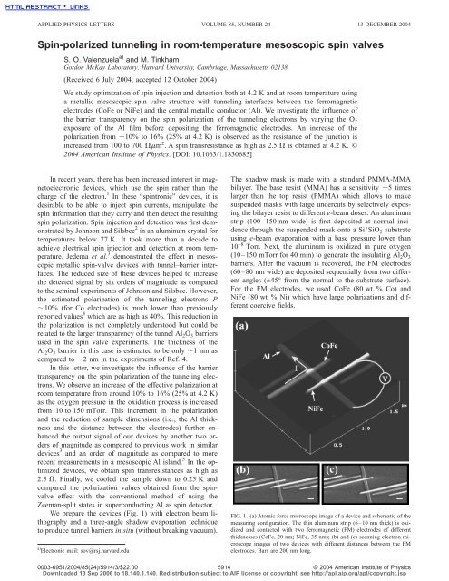
APPLIED PHYSICS LETTERS VOLUME 85, NUMBER 24 13 DECEMBER 2004<strong>Sp<strong>in</strong></strong>-<strong>polarized</strong> <strong>tunnel<strong>in</strong>g</strong> <strong>in</strong> <strong>room</strong>-<strong>temperature</strong> <strong>mesoscopic</strong> sp<strong>in</strong> <strong>valves</strong>S. O. Valenzuela a) and M. T<strong>in</strong>khamGordon McKay Laboratory, Harvard University, Cambridge, Massachusetts 02138(Received 6 July 2004; accepted 12 October 2004)We study optimization of sp<strong>in</strong> <strong>in</strong>jection and detection both at 4.2 K and at <strong>room</strong> <strong>temperature</strong> us<strong>in</strong>ga metallic <strong>mesoscopic</strong> sp<strong>in</strong> valve structure with <strong>tunnel<strong>in</strong>g</strong> <strong>in</strong>terfaces between the ferromagneticelectrodes (CoFe or NiFe) and the central metallic conductor (Al). We <strong>in</strong>vestigate the <strong>in</strong>fluence ofthe barrier transparency on the sp<strong>in</strong> polarization of the <strong>tunnel<strong>in</strong>g</strong> electrons by vary<strong>in</strong>g the O 2exposure of the Al film before deposit<strong>in</strong>g the ferromagnetic electrodes. An <strong>in</strong>crease of thepolarization from 10% to 16% (25% at 4.2 K) is observed as the resistance of the junction is<strong>in</strong>creased from 100 to 700 m 2 . A sp<strong>in</strong> transresistance as high as 2.5 is obta<strong>in</strong>ed at 4.2 K. ©2004 American Institute of Physics. [DOI: 10.1063/1.1830685]In recent years, there has been <strong>in</strong>creased <strong>in</strong>terest <strong>in</strong> magnetoelectronicdevices, which use the sp<strong>in</strong> rather than thecharge of the electron. 1 In these “sp<strong>in</strong>tronic” devices, it isdesirable to be able to <strong>in</strong>ject sp<strong>in</strong> currents, manipulate thesp<strong>in</strong> <strong>in</strong>formation that they carry and then detect the result<strong>in</strong>gsp<strong>in</strong> polarization. <strong>Sp<strong>in</strong></strong> <strong>in</strong>jection and detection was first demonstratedby Johnson and Silsbee 2 <strong>in</strong> an alum<strong>in</strong>um crystal for<strong>temperature</strong>s below 77 K. It took more than a decade toachieve electrical sp<strong>in</strong> <strong>in</strong>jection and detection at <strong>room</strong> <strong>temperature</strong>.Jedema et al. 3 demonstrated the effect <strong>in</strong> <strong>mesoscopic</strong>metallic sp<strong>in</strong>-valve devices with tunnel–barrier <strong>in</strong>terfaces.The reduced size of these devices helped to <strong>in</strong>creasethe detected signal by six orders of magnitude as comparedto the sem<strong>in</strong>al experiments of Johnson and Silsbee. However,the estimated polarization of the <strong>tunnel<strong>in</strong>g</strong> electrons P10% (for Co electrodes) is much lower than previouslyreported values 4 which are as high as 40%. This reduction <strong>in</strong>the polarization is not completely understood but could berelated to the larger transparency of the tunnel Al 2 O 3 barriersused <strong>in</strong> the sp<strong>in</strong> valve experiments. The thickness of theAl 2 O 3 barrier <strong>in</strong> this case is estimated to be only 1 nmascompared to 2 nm <strong>in</strong> the experiments of Ref. 4.In this letter, we <strong>in</strong>vestigate the <strong>in</strong>fluence of the barriertransparency on the sp<strong>in</strong> polarization of the <strong>tunnel<strong>in</strong>g</strong> electrons.We observe an <strong>in</strong>crease of the effective polarization at<strong>room</strong> <strong>temperature</strong> from around 10% to 16% (25% at 4.2 K)as the oxygen pressure <strong>in</strong> the oxidation process is <strong>in</strong>creasedfrom 10 to 150 mTorr. This <strong>in</strong>crement <strong>in</strong> the polarizationand the reduction of sample dimensions (i.e., the Al thicknessand the distance between the electrodes) further enhancedthe output signal of our devices by another two ordersof magnitude as compared to previous work <strong>in</strong> similardevices 3 and an order of magnitude as compared to morerecent measurements <strong>in</strong> a <strong>mesoscopic</strong> Al island. 5 In the optimizeddevices, we obta<strong>in</strong> sp<strong>in</strong> transresistances as high as2.5 . F<strong>in</strong>ally, we cooled the sample down to 0.25 K andcompared the polarization values obta<strong>in</strong>ed from the sp<strong>in</strong>valveeffect with the conventional method of us<strong>in</strong>g theZeeman-split states <strong>in</strong> superconduct<strong>in</strong>g Al as sp<strong>in</strong> detector.We prepare the devices (Fig. 1) with electron beam lithographyand a three-angle shadow evaporation techniqueto produce tunnel barriers <strong>in</strong> situ (without break<strong>in</strong>g vacuum).a) Electronic mail: sov@rsj.harvard.eduThe shadow mask is made with a standard PMMA-MMAbilayer. The base resist (MMA) has a sensitivity 5 timeslarger than the top resist (PMMA) which allows to makesuspended masks with large undercuts by selectively expos<strong>in</strong>gthe bilayer resist to different e-beam doses. An alum<strong>in</strong>umstrip (100–150 nm wide) is first deposited at normal <strong>in</strong>cidencethrough the suspended mask onto a Si/SiO 2 substrateus<strong>in</strong>g e-beam evaporation with a base pressure lower than10 −8 Torr. Next, the alum<strong>in</strong>um is oxidized <strong>in</strong> pure oxygen(10–150 mTorr for 40 m<strong>in</strong>) to generate the <strong>in</strong>sulat<strong>in</strong>g Al 2 O 3barriers. After the vacuum is recovered, the FM electrodes(60–80 nm wide) are deposited sequentially from two differentangles (±45° from the normal to the substrate surface).For the FM electrodes, we used CoFe (80 wt. % Co) andNiFe (80 wt. % Ni) which have large polarizations and differentcoercive fields.FIG. 1. (a) Atomic force microscope image of a device and schematic of themeasur<strong>in</strong>g configuration. The th<strong>in</strong> alum<strong>in</strong>um strip (6–10 nm thick) is oxidizedand contacted with two ferromagnetic (FM) electrodes of differentthicknesses (CoFe, 20 nm; NiFe, 35 nm); (b) and (c) scann<strong>in</strong>g electron microscopeimages of two devices with different distances between the FMelectrodes. Bars are 200 nm long.0003-6951/2004/85(24)/5914/3/$22.00 © 2004 American Institute of Physics5914Downloaded 13 Sep 2006 to 18.140.1.140. Redistribution subject to AIP license or copyright, see http://apl.aip.org/apl/copyright.jsp
Appl. Phys. Lett., Vol. 85, No. 24, 13 December 2004 S. O. Valenzuela and M. T<strong>in</strong>kham 5915Tunnel junctions form at the overlapp<strong>in</strong>g regions withthe Al strip with an area resistance <strong>in</strong> the range of100–700 m 2 depend<strong>in</strong>g on the oxygen exposure.Samples made under the same conditions typically presenteda variation below 20% <strong>in</strong> the resistance of the tunnel junctions.The thickness of the NiFe and CoFe electrodes werechosen to be 20 and 35 nm, respectively to geometricallyenhance the difference <strong>in</strong> their coercive fields. A small magneticfield of 60 Oe along the FM electrodes was applieddur<strong>in</strong>g the growth to favor the alignment of their magnetocrystall<strong>in</strong>eand shape anisotropies.We made several sets of four samples; each of them <strong>in</strong> as<strong>in</strong>gle deposition with different oxidation conditions and differentAl thicknesses. The distance d between the FM electrodes(center to center) was varied from 150 to 700 nm. Theactual dimensions of the samples were measured with a scann<strong>in</strong>gelectron microscope (SEM). The estimated conductivityof the Al, Al , for various samples was found to be <strong>in</strong> therange 0.3–1.110 7 −1 m −1 and <strong>in</strong>creased with the thicknessof the Al film 6–10 nm. The samples were classifiedas a function of the tunnel junction resistances. We discardedsamples show<strong>in</strong>g an anomalously different resistance <strong>in</strong> anyof the two junctions as compared to the rest of the samples <strong>in</strong>their correspond<strong>in</strong>g batch.In our experiments, we source sp<strong>in</strong>-<strong>polarized</strong> electrons<strong>in</strong>to the alum<strong>in</strong>um (Al) strip from one of the FM electrodes[CoFe <strong>in</strong> Fig. 1(a)]. A current I from or <strong>in</strong>to the source results<strong>in</strong> an unequal density of sp<strong>in</strong>-up and sp<strong>in</strong>-down electrons<strong>in</strong> the alum<strong>in</strong>um 2,3 with a difference proportional to theeffective polarization of the CoFe electrode, P CoFe , whichcharacterizes the difference between the sp<strong>in</strong>-up and sp<strong>in</strong>downpopulations of the electrons that participate <strong>in</strong> the <strong>tunnel<strong>in</strong>g</strong>.For low bias, P CoFe can be written as P CoFe =N ↑−N ↓ /N ↑ +N ↓ where N ↑,↓ are the electronic sp<strong>in</strong>-up (↑) andsp<strong>in</strong>-down (↓) density of states at the Fermi level of the<strong>tunnel<strong>in</strong>g</strong> electrons <strong>in</strong> the FM (CoFe).The sp<strong>in</strong> imbalance created by the current will diffuse <strong>in</strong>both directions along the Al strip and will reach the detectorelectrode (NiFe) which will measure an average of the twosp<strong>in</strong> densities weighted by its own polarization, P NiFe . Therefore,the output voltage V is sensitive to the sp<strong>in</strong> degree offreedom 2,3 and is proportional to P CoFe P NiFe . More explicitly,the magnitude of the output transresistance V/I is equalto: 2,3 V ±I =±1 2 P sfCoFeP NiFe Al A e−d/ sf,1where sf is the sp<strong>in</strong> relaxation length and Al and A are theconductivity and cross sectional area of the Al strip. Here the() and () signs correspond to parallel and antiparallelconfigurations of the electrodes magnetizations. The sp<strong>in</strong> relaxationlength can be obta<strong>in</strong>ed by fitt<strong>in</strong>g the transresistanceas a function of d to Eq. (1). The geometric mean P of thepolarization of the electrodes P= PCoFe P NiFe is then calculatedus<strong>in</strong>g sf . It is worth not<strong>in</strong>g that we measured severalsamples each with a s<strong>in</strong>gle pair of FM electrodes with adef<strong>in</strong>ite spac<strong>in</strong>g d as opposed to one sample with multipleelectrodes <strong>in</strong> order to avoid possible anomalous sp<strong>in</strong>-flipscatter<strong>in</strong>g at the <strong>in</strong>terfaces with each FM.The measurements were performed us<strong>in</strong>g lock-<strong>in</strong> techniquesby apply<strong>in</strong>g a current I1 A through the sourcejunction and measur<strong>in</strong>g ac voltage at the remote detectorFIG. 2. (a) <strong>Sp<strong>in</strong></strong>-valve transresistance V/I for two samples: one at 4.2 K(larger variation) and the other at <strong>room</strong> <strong>temperature</strong> (RT), I=1 A; (b)logarithm of the sp<strong>in</strong> transresistance change R=V/I as a function of thedistance d between the ferromagnetic electrodes for four sets of samples.The top curve (open circles) was taken at 4.2 K the rest at RT. The thicknessof the Al strip is 10 nm (triangles) and 6 nm (open and solid circles anddiamonds). The l<strong>in</strong>es are fitt<strong>in</strong>gs to Eq. (1). Inset: R as a function ofcurrent bias for a sample with d=215 nm at T=4.2 K. A significant drop <strong>in</strong>R is seen for I1 A.junction as sketched <strong>in</strong> Fig. 1(a). The results are <strong>in</strong>dependentof which electrode is used as source or detector. For largerbiases, we found that the effective polarization drops 6 [see<strong>in</strong>set of Fig. 2(b)]. In this letter, we concentrate on the lowbias response.Figure 2(a) shows typical sp<strong>in</strong>-valve transresistance V/Imeasurements at 4.2 K and at <strong>room</strong> <strong>temperature</strong> as a functionof an applied <strong>in</strong>-plane field along the axis of the FMelectrodes. At large negative magnetic field we have a parallelconfiguration of the electrodes magnetization and R=V + /I. As the magnetic field is swept from negative to positive,a change <strong>in</strong> the sign of the detector signal is observedwhen the magnetization of the NiFe electrode reverses andthe device switches from parallel to antiparallel configurationR=V − /I=−V + /I. As the magnetic field is further <strong>in</strong>creasedthe CoFe flips and the detector signal changes sign aga<strong>in</strong> asa parallel configuration is recovered.Figure 2(b) shows the change <strong>in</strong> output sp<strong>in</strong> transresistanceR=V + −V − /I as a function of d for different sets ofsamples. By fitt<strong>in</strong>g the data to Eq. (1), we calculate sf andP. The product Al A is obta<strong>in</strong>ed <strong>in</strong>dependently by measur<strong>in</strong>gd (with a SEM) and the resistance between the FM electrodes,R Al A=d/R. Our measurements show transresistancesas high as 2.5 4.2 K for the samples with thelargest effective polarization (25%) and with the smallest d.The polarization drops to around 16%–17% at <strong>room</strong> <strong>temperature</strong>.Although no reduction <strong>in</strong> P was observed <strong>in</strong> Ref. 3,a similar reduction has been found <strong>in</strong> the magnetoresistance<strong>in</strong> metallic magnetic tunnel junctions which was ascribed toa loss of magnetization at large <strong>temperature</strong>s due to magnonexcitations at the FM-barrier <strong>in</strong>terface 7 and thermally assistedsp<strong>in</strong>-<strong>in</strong>dependent <strong>tunnel<strong>in</strong>g</strong>. 8It is <strong>in</strong>terest<strong>in</strong>g to note that for the th<strong>in</strong> Al strip 6 nmthe slope of the l<strong>in</strong>es <strong>in</strong> Fig. 2(b) does not change with <strong>temperature</strong>and, as expected, it is <strong>in</strong>dependent of the barriertransparency. In all cases, the fitted sp<strong>in</strong> relaxation length, sf , is around 200 nm. Measurements performed on thickerAl strips 10 nm, open triangles <strong>in</strong> Fig. 2(b), presented alarger sf 420 nm suggest<strong>in</strong>g that the sp<strong>in</strong>-flip <strong>in</strong> the th<strong>in</strong>nersamples is dom<strong>in</strong>ated by surface scatter<strong>in</strong>g.More important, we also found a systematic <strong>in</strong>crease <strong>in</strong>the sp<strong>in</strong> polarization as the barrier transparency decreased(higher O 2 pressure <strong>in</strong> the barrier preparation). This is clearlyDownloaded 13 Sep 2006 to 18.140.1.140. Redistribution subject to AIP license or copyright, see http://apl.aip.org/apl/copyright.jsp
5916 Appl. Phys. Lett., Vol. 85, No. 24, 13 December 2004 S. O. Valenzuela and M. T<strong>in</strong>khamFIG. 3. (a) Calculated polarization P by fitt<strong>in</strong>g the sp<strong>in</strong>-valve transresistancedependence on the distance between the ferromagnetic electrodes to Eq. (1).Lowest resistance polarization value is from Ref. 3. The l<strong>in</strong>e is a guide to theeye: (b) and (c) experimental dI/dV curves at 0.25 K for 0 T (open circles)and 2 T (solid circles). NiFe (b); CoFe (c). These are four probe measurementswith a 4 V, 42.2 Hz s<strong>in</strong>e voltage.represented <strong>in</strong> Fig. 3(a) and it could be relevant to understandwhy the polarization reported <strong>in</strong> Ref. 3 is lower than <strong>in</strong>previous studies. 5 It is generally accepted that the sp<strong>in</strong> polarizationis dom<strong>in</strong>ated by sp-like electrons because of theirlarge contribution to the <strong>tunnel<strong>in</strong>g</strong> due to their highly delocalizednature 9,10 (as compared to d electrons). However, areduction of the effective <strong>tunnel<strong>in</strong>g</strong> polarization could be expectedif th<strong>in</strong>ner barriers lead to an <strong>in</strong>creased contribution tothe <strong>tunnel<strong>in</strong>g</strong> of the highly localized d states (see, for example,Refs. 11 and 12). P<strong>in</strong>holes <strong>in</strong> the barriers and achange <strong>in</strong> the barrier height 13 could also lead to a reduction<strong>in</strong> the polarization. P<strong>in</strong>holes, however, are unlikely to be responsibleas no leakage current is observed <strong>in</strong> our conductancemeasurements at low <strong>temperature</strong> 12 [see below andFigs. 3(b) and 3(c)]. The general behavior of sp<strong>in</strong> <strong>polarized</strong>free-electron models should be analyzed as a function of thetunnel-barrier properties. Experimentally, a systematic studyof the bias dependence of the polarization for different oxidationtimes would provide valuable <strong>in</strong>formation on the natureof the <strong>tunnel<strong>in</strong>g</strong> electrons.F<strong>in</strong>ally, we used the traditional Meservey-Tedrowtechnique 4 to readily measure the <strong>tunnel<strong>in</strong>g</strong> polarization ofour junctions and compare it with the values obta<strong>in</strong>ed above.This technique is limited to low <strong>temperature</strong>s, below the superconduct<strong>in</strong>gcritical <strong>temperature</strong> of the Al strip. The Zeemansplitt<strong>in</strong>g <strong>in</strong> the density of states of the superconductor,<strong>in</strong>duced by a large magnetic field, is used as a sp<strong>in</strong> detector.The orbital depair<strong>in</strong>g <strong>in</strong> the samples with the th<strong>in</strong>nest Al isstrongly reduced when the magnetic field is applied <strong>in</strong> thesubstrate plane. The <strong>tunnel<strong>in</strong>g</strong> junctions were cooled down to0.25 K and the <strong>tunnel<strong>in</strong>g</strong> conductance was measured at zerofield and at 2 T.Figures 3(b) and 3(c) show the differential <strong>tunnel<strong>in</strong>g</strong>conductance curves for a typical NiFe [(b)] and CoFe [(c)]junction. At H=0, the conductance exhibits the typical goodqualityjunction behavior, present<strong>in</strong>g no leakage current atzero voltage. Zeeman splitt<strong>in</strong>g of the quasiparticle density ofstates is clearly seen at H=2 T. The asymmetry <strong>in</strong> the conductancecurve <strong>in</strong> this case is used to extract the value of thepolarization of the ferromagnet. A rough estimate of the sp<strong>in</strong>orbitcorrected polarization can be obta<strong>in</strong>ed 4,14 from theheight of the four conductance peaks namely, P CoFe =48%and P NiFe =29%. Their geometrical average is 37% which islarger than the value obta<strong>in</strong>ed from Eq. (1) for the samesample (25%). It is worth not<strong>in</strong>g that this rough calculationhas been found 14 to systematically overestimate the actualpolarization by 5%–10% and a more careful fitt<strong>in</strong>g of thedata of Figs. 3(b) and 3(c) would be required for more accuratevalues. With a 10% reduction <strong>in</strong> the above estimatedvalues of P CoFe and P NiFe , P27% is <strong>in</strong> closer agreementwith the fitt<strong>in</strong>g to Eq. (1) at 4.2 K. A detailed analysis and acomparison between the values of P obta<strong>in</strong>ed with these experimentsis important and will be reported elsewhere.In summary, we have demonstrated sp<strong>in</strong> <strong>in</strong>jection anddetection <strong>in</strong> <strong>mesoscopic</strong> sp<strong>in</strong> <strong>valves</strong> both at <strong>room</strong> <strong>temperature</strong>and 4.2 K. We found that for low transparency barriersthe polarization of the <strong>in</strong>jected electrons grows. For the lowtransparency barriers, we obta<strong>in</strong>ed sp<strong>in</strong> transresistances ashigh as 2.5 .The authors thank John U. Free for a careful read<strong>in</strong>g ofthe manuscript. This research was supported <strong>in</strong> part by NSFGrant Nos. DMR-0244441 and NSECPHY-0117795 andONR Grant No. N00014-02-1-0055.1 For a recent review see, I. Žutić, J. Fabian, and S. Das Sarma, Rev. Mod.Phys. 76, 323(2004).2 M. Johnson and R. H. Silsbee, Phys. Rev. Lett. 55, 1790 (1985); Phys.Rev. B 35, 4959 (1987); Phys. Rev. B 37, 5236(1988).3 F. J. Jedema, H. B. Heersche, A. T. Filip, J. J. A. Baselmans, and B. J. vanWees, Nature (London) 416, 713 (2002); F. J. Jedema, M. V. Costache, H.B. Heersche, J. J. A. Baselmans, and B. J. van Wees, Appl. Phys. Lett. 81,5162 (2002).4 R. Meservey and P. M. Tedrow, Phys. Rep. 238, 173 (1994).5 M. Zaffalon and B. J. van Wees, Phys. Rev. Lett. 410, 345 (2003).6 This effect is analyzed <strong>in</strong> S. O. Valenzuela, D. J. Monsma, C. M. Marcus,V. Narayanamurti, and M. T<strong>in</strong>kham (unpublished).7 S. Zhang, P. M. Levy, A. C. Marley, and S. S. P. Park<strong>in</strong>, Phys. Rev. Lett.79, 3744 (1997).8 J. S. Moodera, J. Nowak, and R. J.M. van de Veerdonk, Phys. Rev. Lett.80, 2941 (1998).9 J. A. Hertz and K. Aoi, Phys. Rev. B 8, 3252(1973).10 M. B. Stearns, J. Magn. Magn. Mater. 5, 167 (1977).11 S. F. Alvarado, Phys. Rev. Lett. 75, 513(1995).12 M. Müzemberg and J. S. Moodera, Phys. Rev. B 70, 060402R (2004).13 J. C. Slonczewski, Phys. Rev. B 39, 6995 (1989).14 D. J. Monsma and S. S.P. Park<strong>in</strong>, Appl. Phys. Lett. 77, 720(2000).Downloaded 13 Sep 2006 to 18.140.1.140. Redistribution subject to AIP license or copyright, see http://apl.aip.org/apl/copyright.jsp