

CHARPAN - FFG 7. Rahmenprogramm
CHARPAN - FFG 7. Rahmenprogramm
CHARPAN - FFG 7. Rahmenprogramm

You also want an ePaper? Increase the reach of your titles
YUMPU automatically turns print PDFs into web optimized ePapers that Google loves.
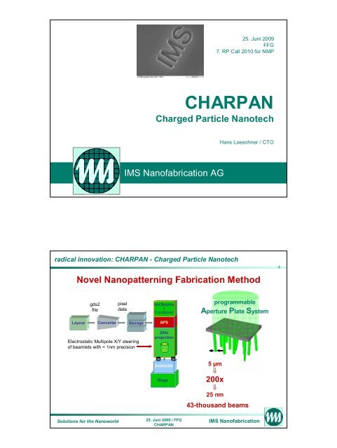
Layout Converter<br />
Storage<br />
Solutions for the Nanoworld<br />
IMS Nanofabrication AG<br />
25. Juni 2009<br />
<strong>FFG</strong><br />
<strong>7.</strong> RP Call 2010 für NMP<br />
<strong>CHARPAN</strong><br />
Charged Particle Nanotech<br />
radical innovation: <strong>CHARPAN</strong> - Charged Particle Nanotech<br />
Ion Source<br />
&<br />
Condenser<br />
APS<br />
200x<br />
projection<br />
Substrate<br />
Stage<br />
25. Juni 2009 / <strong>FFG</strong><br />
<strong>CHARPAN</strong><br />
Hans Loeschner / CTO<br />
Novel Nanopatterning Fabrication Method<br />
gds2<br />
file<br />
pixel<br />
data<br />
Electrostatic Multipole X/Y steering<br />
of beamlets with < 1nm precision<br />
programmable<br />
Aperture Plate System<br />
5 µm<br />
⇓<br />
200x<br />
⇓<br />
25 nm<br />
43-thousand beams<br />
IMS Nanofabrication<br />
2
Project idea and coordinator: IMS Nanofabrication / SME<br />
Project filing (stage 1 and stage 2): 2004 (FP6 – NMP, 3rd call)<br />
• Guidance and financial support: Gerald Kern / <strong>FFG</strong><br />
• Project filing support: Moshe Harel / Consultant (Israel)<br />
Dieter Meinhard, Andrea Kurz, Walter Aigner / HiTec<br />
Project duration: April 2005 – March 2009<br />
Project costs: 16.59 Mio Euro<br />
EC funding: 9.50 Mio Euro<br />
Project Management:<br />
Elmar Platzgummer Karin Schuster Hans Loeschner<br />
Project Financial Project<br />
Manager Administration Administrator<br />
Solutions for the Nanoworld<br />
Solutions for the Nanoworld<br />
idea � project<br />
25. Juni 2009 / <strong>FFG</strong><br />
<strong>CHARPAN</strong><br />
Consortium<br />
IMS Nanofabrication<br />
(coordinator)<br />
25. Juni 2009 / <strong>FFG</strong><br />
<strong>CHARPAN</strong><br />
IMS Nanofabrication<br />
Australia<br />
IMS Nanofabrication<br />
3<br />
4
ealized <strong>CHARPAN</strong> Tool<br />
programmable<br />
Aperture Plate System<br />
2.5 µm<br />
⇓<br />
200x<br />
⇓<br />
12.5 nm<br />
Solutions for the Nanoworld<br />
25. Juni 2009 / <strong>FFG</strong><br />
<strong>CHARPAN</strong><br />
Ion Source<br />
Condenser Ion Optics<br />
Ion Beam<br />
Projection Optics<br />
with<br />
200x Reduction<br />
realized: 43-thousand programmable beams of 12.5 nm beam size<br />
(2-times better compared to orginal target)<br />
IMS Nanofabrication<br />
<strong>CHARPAN</strong> 43k-APS exposure result: 10keV H 3 + ions� 50nm HSQ resist<br />
gds2 file<br />
(provided by Falco van Delft,<br />
PHILIPS Research, MiPlaza,<br />
Eindhoven, The Netherlands)<br />
Solutions for the Nanoworld<br />
25. Juni 2009 / <strong>FFG</strong><br />
<strong>CHARPAN</strong><br />
<strong>CHARPAN</strong> exposed HSQ<br />
non-chemically amplified<br />
resist on 150mm Si wafer<br />
(20 µm x 20 µm exposure field)<br />
IMS Nanofabrication<br />
5<br />
6
<strong>CHARPAN</strong> 43k-APS exposure result: 10keV H 3 + � 50nm HSQ<br />
1:2 patterns<br />
(line : space)<br />
50nm HSQ<br />
150mm Si Wafer<br />
10 keV H +<br />
3<br />
100 µA/cm2 ,<br />
exposure dose:<br />
20 µC/cm2 Solutions for the Nanoworld<br />
25. Juni 2009 / <strong>FFG</strong><br />
<strong>CHARPAN</strong><br />
30 nm<br />
20nm<br />
10nm<br />
IMS Nanofabrication<br />
<strong>CHARPAN</strong> 43k-APS exposure result: 10keV H 3 + � 50nm HSQ<br />
gds2 file<br />
50nm HSQ<br />
150mm Si Wafer<br />
10 keV H +<br />
3<br />
100 µA/cm2 ,<br />
exposure dose:<br />
20 µC/cm2 Solutions for the Nanoworld<br />
25. Juni 2009 / <strong>FFG</strong><br />
<strong>CHARPAN</strong><br />
IMS Nanofabrication<br />
7<br />
8
<strong>CHARPAN</strong> 43k-APS exposure result: 10keV H 3 + � 20nm HSQ<br />
gds2 file<br />
20nm HSQ<br />
150mm Si Wafer<br />
10 keV H +<br />
3<br />
100 µA/cm2 ,<br />
exposure dose:<br />
45 µC/cm2 Solutions for the Nanoworld<br />
<strong>CHARPAN</strong> Application Fields<br />
Leading-Edge Complex<br />
Masks<br />
for sub-22nm hp<br />
Optical Lithography<br />
Solutions for the Nanoworld<br />
Master Stamp for NIL:<br />
< 20 nm dots @ 62.5 nm pitch<br />
25. Juni 2009 / <strong>FFG</strong><br />
<strong>CHARPAN</strong><br />
<strong>CHARPAN</strong><br />
Charged Particle Nanotech<br />
2D & 3D Nano-Imprint<br />
Master Templates<br />
for NIL<br />
(Nano-Imprint Lithography)<br />
25. Juni 2009 / <strong>FFG</strong><br />
<strong>CHARPAN</strong><br />
IMS Nanofabrication<br />
Maskless<br />
Nanolithography<br />
&<br />
3D Resistless<br />
Nanopatterning<br />
Existing SC Markets Emerging Nanotechnology Markets<br />
• Nano-Photonics Devices<br />
• Nano-Biotechnology Devices<br />
• Nano-Magnetic Devices<br />
• Nano-Sensoric Devices<br />
IMS Nanofabrication<br />
9<br />
10
Acknowledgements<br />
� This work has been supported by<br />
� The European Commission / 6 th Framework Programme (FP6<br />
� The Austrian Research Promotion Agency<br />
Solutions for the Nanoworld<br />
Solutions for the Nanoworld<br />
Thank You for Your Attention !<br />
25. Juni 2009 / <strong>FFG</strong><br />
<strong>CHARPAN</strong><br />
Diskussion<br />
www.ims.co.at<br />
IMS Nanofabrication<br />
Hat IMS Nanofabrication durch dieses Projekt profitiert ?<br />
Haben andere Partner im Konsortium ebenfalls durch<br />
dieses Projekt profitiert ?<br />
Wie geht es mit dieser Technologie weiter ?<br />
Wäre <strong>CHARPAN</strong> mit nationalen Mitteln (z.B. Nanoinitiative)<br />
umsetzbar gewesen ?<br />
Würde IMS Nanofabrication <strong>CHARPAN</strong> noch einmal<br />
durchführen ?<br />
Vorteile / Nachteile des <strong>Rahmenprogramm</strong>s aus Sicht von<br />
IMS Nanofabrication AG<br />
25. Juni 2009 / <strong>FFG</strong><br />
<strong>CHARPAN</strong><br />
IMS Nanofabrication<br />
11<br />
12
![NILaustria_web_01 [Compatibility Mode]](https://img.yumpu.com/4631581/1/190x135/nilaustria-web-01-compatibility-mode.jpg?quality=85)