LSH33 32-bit Barrel Shifter with Registers - Datasheet
LSH33 32-bit Barrel Shifter with Registers - Datasheet
LSH33 32-bit Barrel Shifter with Registers - Datasheet

You also want an ePaper? Increase the reach of your titles
YUMPU automatically turns print PDFs into web optimized ePapers that Google loves.
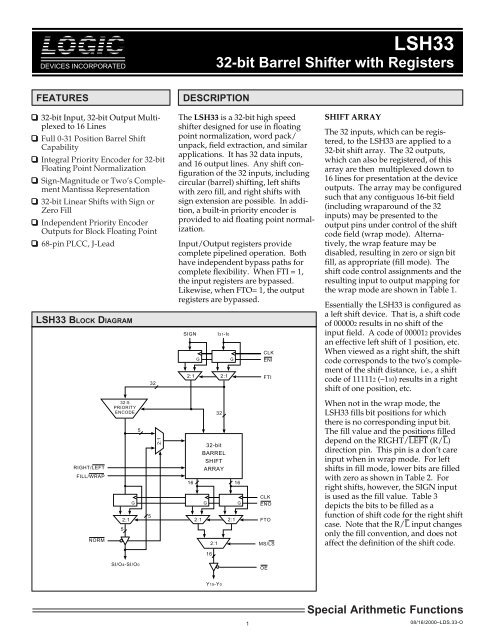
DEVICES INCORPORATEDDEVICES INCORPORATED<strong>LSH33</strong><strong>32</strong>-<strong>bit</strong> <strong>Barrel</strong> <strong>Shifter</strong> <strong>with</strong> <strong>Registers</strong><strong>LSH33</strong><strong>32</strong>-<strong>bit</strong> <strong>Barrel</strong> <strong>Shifter</strong> <strong>with</strong> <strong>Registers</strong>FEATURESDESCRIPTION❑ <strong>32</strong>-<strong>bit</strong> Input, <strong>32</strong>-<strong>bit</strong> Output Multiplexedto 16 Lines❑ Full 0-31 Position <strong>Barrel</strong> ShiftCapability❑ Integral Priority Encoder for <strong>32</strong>-<strong>bit</strong>Floating Point Normalization❑ Sign-Magnitude or Two’s ComplementMantissa Representation❑ <strong>32</strong>-<strong>bit</strong> Linear Shifts <strong>with</strong> Sign orZero Fill❑ Independent Priority EncoderOutputs for Block Floating Point❑ 68-pin PLCC, J-Lead<strong>LSH33</strong> BLOCK DIAGRAMRIGHT/LEFTFILL/WRAPNORM<strong>32</strong>:5PRIORITYENCODE <strong>32</strong>52:1G55<strong>32</strong>2:1The <strong>LSH33</strong> is a <strong>32</strong>-<strong>bit</strong> high speedshifter designed for use in floatingpoint normalization, word pack/unpack, field extraction, and similarapplications. It has <strong>32</strong> data inputs,and 16 output lines. Any shift configurationof the <strong>32</strong> inputs, includingcircular (barrel) shifting, left shifts<strong>with</strong> zero fill, and right shifts <strong>with</strong>sign extension are possible. In addition,a built-in priority encoder isprovided to aid floating point normalization.Input/Output registers providecomplete pipelined operation. Bothhave independent bypass paths forcomplete flexibility. When FTI = 1,the input registers are bypassed.Likewise, when FTO= 1, the outputregisters are bypassed.SIGNG2:1 2:116<strong>32</strong>-<strong>bit</strong>BARRELSHIFTARRAYG162:1I31-I0G2:1 2:116GCLKENIFTICLKENOFTOMS/LSSHIFT ARRAYThe <strong>32</strong> inputs, which can be registered,to the <strong>LSH33</strong> are applied to a<strong>32</strong>-<strong>bit</strong> shift array. The <strong>32</strong> outputs,which can also be registered, of thisarray are then multiplexed down to16 lines for presentation at the deviceoutputs. The array may be configuredsuch that any contiguous 16-<strong>bit</strong> field(including wraparound of the <strong>32</strong>inputs) may be presented to theoutput pins under control of the shiftcode field (wrap mode). Alternatively,the wrap feature may bedisabled, resulting in zero or sign <strong>bit</strong>fill, as appropriate (fill mode). Theshift code control assignments and theresulting input to output mapping forthe wrap mode are shown in Table 1.Essentially the <strong>LSH33</strong> is configured asa left shift device. That is, a shift codeof 000002 results in no shift of theinput field. A code of 000012 providesan effective left shift of 1 position, etc.When viewed as a right shift, the shiftcode corresponds to the two’s complementof the shift distance, i.e., a shiftcode of 111112 (–110) results in a rightshift of one position, etc.When not in the wrap mode, the<strong>LSH33</strong> fills <strong>bit</strong> positions for whichthere is no corresponding input <strong>bit</strong>.The fill value and the positions filleddepend on the RIGHT/LEFT (R/L)direction pin. This pin is a don’t careinput when in wrap mode. For leftshifts in fill mode, lower <strong>bit</strong>s are filled<strong>with</strong> zero as shown in Table 2. Forright shifts, however, the SIGN inputis used as the fill value. Table 3depicts the <strong>bit</strong>s to be filled as afunction of shift code for the right shiftcase. Note that the R/L input changesonly the fill convention, and does notaffect the definition of the shift code.SI/O4-SI/O0OEY15-Y01Special Arithmetic Functions08/16/2000–LDS.33-O
DEVICES INCORPORATED<strong>LSH33</strong><strong>32</strong>-<strong>bit</strong> <strong>Barrel</strong> <strong>Shifter</strong> <strong>with</strong> <strong>Registers</strong>TABLE 1. WRAP MODE SHIFT CODE DEFINITIONSShift Code Y 31 Y 30 Y 29 ••• Y 16 Y 15 ••• Y 2 Y 1 Y 000000 I31 I30 I29 ••• I16 I15 ••• I2 I1 I000001 I30 I29 I28 ••• I15 I14 ••• I1 I0 I3100010 I29 I28 I27 ••• I14 I13 ••• I0 I31 I3000011 I28 I27 I26 ••• I13 I12 ••• I31 I30 I29• • • • ••• • • ••• • • •• • • • ••• • • ••• • • •• • • • ••• • • ••• • • •01111 I16 I15 I14 ••• I1 I0 ••• I19 I18 I1710000 I15 I14 I13 ••• I0 I31 ••• I18 I17 I1610001 I14 I13 I12 ••• I31 I30 ••• I17 I16 I1510010 I13 I12 I11 ••• I30 I29 ••• I16 I15 I14• • • • ••• • • ••• • • •• • • • ••• • • ••• • • •• • • • ••• • • ••• • • •11100 I3 I2 I1 ••• I20 I19 ••• I6 I5 I411101 I2 I1 I0 ••• I19 I18 ••• I5 I4 I311110 I1 I0 I31 ••• I18 I17 ••• I4 I3 I211111 I0 I31 I30 ••• I17 I16 ••• I3 I2 I1TABLE 2. FILL MODE SHIFT CODE DEFINITIONS — LEFT SHIFTShift Code Y 31 Y 30 Y 29 ••• Y 16 Y 15 ••• Y 2 Y 1 Y 000000 I31 I30 I29 ••• I16 I15 ••• I2 I1 I000001 I30 I29 I28 ••• I15 I14 ••• I1 I0 000010 I29 I28 I27 ••• I14 I13 ••• I0 0 000011 I28 I27 I26 ••• I13 I12 ••• 0 0 0• • • • ••• • • ••• • • •• • • • ••• • • ••• • • •• • • • ••• • • ••• • • •01111 I16 I15 I14 ••• I1 I0 ••• 0 0 010000 I15 I14 I13 ••• I0 0 ••• 0 0 010001 I14 I13 I12 ••• 0 0 ••• 0 0 010010 I13 I12 I11 ••• 0 0 ••• 0 0 0• • • • ••• • • ••• • • •• • • • ••• • • ••• • • •• • • • ••• • • ••• • • •11100 I3 I2 I1 ••• 0 0 ••• 0 0 011101 I2 I1 I0 ••• 0 0 ••• 0 0 011110 I1 I0 0 ••• 0 0 ••• 0 0 011111 I0 0 0 ••• 0 0 ••• 0 0 0In fill mode, as in wrap mode, the shiftcode input represents the number ofshift positions directly for left shifts,but the two’s complement of the shiftcode results in the equivalent rightshift. However, for fill mode the R/Linput can be viewed as the mostsignificant <strong>bit</strong> of a 6-<strong>bit</strong> two’s complementshift code, comprised of R/Lconcatenated <strong>with</strong> the SI4–SI0 lines.Thus, a positive shift code (R/L = 0)results in a left shift of 0–31 positions,and a negative code (R/L = 1) a rightshift of up to <strong>32</strong> positions. The <strong>LSH33</strong>can thus effectively select any contiguous<strong>32</strong>-<strong>bit</strong> field out of a (sign extendedand zero filled) 96-<strong>bit</strong> "input."OUTPUT MULTIPLEXERThe shift array outputs can be registeredand then applied to a 2:1 multiplexercontrolled by the MS/LS selectline. This multiplexer makes availableat the output pins either the mostsignificant or least significant 16outputs of the shift array.PRIORITY ENCODERThe <strong>32</strong>-<strong>bit</strong> input bus drives a priorityencoder which is used to determinethe first significant position forpurposes of normalization. Thepriority encoder produces a five-<strong>bit</strong>code representing the location of thefirst non-zero <strong>bit</strong> in the input word.Code assignment is such that thepriority encoder output represents thenumber of shift positions required toleft align the first non-zero <strong>bit</strong> of theinput word. Prior to the priorityencoder, the input <strong>bit</strong>s are individuallyexclusive OR’ed <strong>with</strong> the SIGNinput. This allows normalization infloating point systems using two’scomplement mantissa representation.A negative value in two’s complementrepresentation will cause the exclusiveOR gates to invert the input data tothe encoder. As a result, the leadingsignificant digit will always be "1."Special Arithmetic Functions208/16/2000–LDS.33-O
DEVICES INCORPORATED<strong>LSH33</strong><strong>32</strong>-<strong>bit</strong> <strong>Barrel</strong> <strong>Shifter</strong> <strong>with</strong> <strong>Registers</strong>TABLE 3. FILL MODE SHIFT CODE DEFINITIONS — RIGHT SHIFTShift Code Y 31 Y 30 Y 29 ••• Y 16 Y 15 ••• Y 2 Y 1 Y 000000 S S S ••• S S ••• S S S00001 S S S ••• S S ••• S S I3100010 S S S ••• S S ••• S I31 I3000011 S S S ••• S S ••• I31 I30 I29• • • • ••• • • ••• • • •• • • • ••• • • ••• • • •• • • • ••• • • ••• • • •01111 S S S ••• S S ••• I19 I18 I1710000 S S S ••• S I31 ••• I18 I17 I1610001 S S S ••• I31 I30 ••• I17 I16 I1510010 S S S ••• I30 I29 ••• I16 I15 I14• • • • ••• • • ••• • • •• • • • ••• • • ••• • • •• • • • ••• • • ••• • • •11100 S S S ••• I20 I19 ••• I6 I5 I411101 S S S ••• I19 I18 ••• I5 I4 I311110 S S I31 ••• I18 I17 ••• I4 I3 I211111 S I31 I30 ••• I17 I16 ••• I3 I2 I1TABLE 4. PRIORITY ENCODER FUNCTION TABLEI31I30I29•••I16I15••• I2 I1 I0 Shift Code1 X X ••• X X ••• X X X 000000 1 X ••• X X ••• X X X 000010 0 1 ••• X X ••• X X X 00010• • • ••• • • ••• • • • •• • • ••• • • ••• • • • •0 0 0 ••• 1 X ••• X X X 011110 0 0 ••• 0 1 ••• X X X 100000 0 0 ••• 0 0 ••• X X X 10001• • • ••• • • ••• • • • •• • • ••• • • ••• • • • •0 0 0 ••• 0 0 ••• 0 1 X 111100 0 0 ••• 0 0 ••• 0 0 1 111110 0 0 ••• 0 0 ••• 0 0 0 11111This affects only the encoder inputs;the shift array always operates on theraw input data. The priority encoderfunction table is shown in Table 4.NORMALIZE MULTIPLEXERThe NORM input, when asserted,results in the priority encoder outputdriving the internal shift code inputsdirectly. When using the NORMfunction, the <strong>LSH33</strong> should be placedin fill mode, <strong>with</strong> the R/L input low.When NORM is high (not asserted),the SI/O4–SI/O0 port acts as the shiftcode input to the shifter.APPLICATIONS EXAMPLESNormalization of mantissas up to <strong>32</strong><strong>bit</strong>s can be accomplished directly by asingle <strong>LSH33</strong>. To do this, the NORMinput is asserted, and fill mode andleft shift are selected. The normalizedmantissa is then available at thedevice output in two 16-<strong>bit</strong> segments,under the control of the output datamultiplexer select, the MS/LS signal.If it is desirable to avoid the necessityof multiplexing output data in 16-<strong>bit</strong>segments, two <strong>LSH33</strong> devices can beused in parallel. Both devices receivethe same input word, <strong>with</strong> the MS/LSselect line of one wired high, and theother low. Each device will thenindependently determine the shiftdistance required for normalization,and the full <strong>32</strong> <strong>bit</strong>s of output data willbe available simultaneously.Special Arithmetic Functions308/16/2000–LDS.33-O
DEVICES INCORPORATED<strong>LSH33</strong><strong>32</strong>-<strong>bit</strong> <strong>Barrel</strong> <strong>Shifter</strong> <strong>with</strong> <strong>Registers</strong>MAXIMUM RATINGS Above which useful life may be impaired (Notes 1, 2, 3, 8)Storage temperature ........................................................................................................... –65°C to +150°COperating ambient temperature ........................................................................................... –55°C to +125°CVCC supply voltage <strong>with</strong> respect to ground ............................................................................ –0.5 V to +7.0VInput signal <strong>with</strong> respect to ground ........................................................................................ –3.0 V to +7.0 VSignal applied to high impedance output ............................................................................... –3.0 V to +7.0 VOutput current into low outputs ............................................................................................................. 25 mALatchup current ............................................................................................................................... > 400 mAOPERATING CONDITIONS To meet specified electrical and switching characteristicsMode Temperature Range (Ambient) Supply VoltageActive Operation, Commercial 0°C to +70°C 4.75 V ≤ VCC ≤ 5.25 VActive Operation, Military –55°C to +125°C 4.50 V ≤ VCC ≤ 5.50 VELECTRICAL CHARACTERISTICS Over Operating Conditions (Note 4)Symbol Parameter Test Condition Min Typ Max UnitVOH Output High Voltage VCC = Min., IOH = –2.0 mA 2.4 VVOL Output Low Voltage VCC = Min., IOL = 8.0 mA 0.4 VVIH Input High Voltage 2.0 VCC VVIL Input Low Voltage (Note 3) 0.0 0.8 VIIX Input Current Ground ≤ VIN ≤ VCC (Note 12) ±20 µAIOZ Output Leakage Current Ground ≤ VOUT ≤ VCC (Note 12) ±20 µAICC1 VCC Current, Dynamic (Notes 5, 6) 10 30 mAICC2 VCC Current, Quiescent (Note 7) 1.5 mASpecial Arithmetic Functions408/16/2000–LDS.33-O
123456789012312345678901231234567890123123456789012312345678901234567890123456712345678901234567890123456712345678901234567890123456712345678901234567890123456712345678901234567890123456712345678901234567890123456712345678901234567890123456712345678901234567890123456712345678901234567890123456712345678901234567890123456712345678901231234567890123123456789012312345678901231234567890123123456789012312345678901231234567890123123456789012312345678901231234567890123123456789012312345678901234567890123456712345678901234567890123456712345678901234567890123456712345678901234567890123456712345678901234567890123456712345678901234567890123456712345678901234567890123456712345678901234567890123456712345678901234567890123456712345678901234567890123456712345678901231234567890123123456789012312345678901231234567890123123456789012312345678901231234567890123DEVICES INCORPORATED<strong>LSH33</strong><strong>32</strong>-<strong>bit</strong> <strong>Barrel</strong> <strong>Shifter</strong> <strong>with</strong> <strong>Registers</strong>SWITCHING CHARACTERISTICS — COMMERCIAL OPERATING RANGE (0°C to +70°C)GUARANTEED MAXIMUM COMBINATIONAL DELAYS Notes 9, 10 (ns)123456789012345678901234567123456789012345678901234567To Output<strong>LSH33</strong>-40*<strong>LSH33</strong>-30123456789012345678901234567<strong>LSH33</strong>-20*123456789012345678901234567123456789012345678901234567123456789012345678901234567From Input123456789012345678901234567123456789012345678901234567Y15-Y0SO4-SO0123456789012345678901234567123456789012345678901234567Y15-Y0SO4-SO0123456789012345678901234567123456789012345678901234567Y15-Y0SO4-SO0123456789012345678901234567123456789012345678901234567123456789012345678901234567FTI = 0, FTO = 0CLKMS/LS12345678901234567890123456712345678901234567890123456712345678901234567890123456712345678901234567890123456728 2828 —12345678901234567890123456712345678901234567890123456712345678901234567890123456712345678901234567890123456712345678901234567890123456724 2424 —12345678901234567890123456712345678901234567890123456715 1515 —123456789012345678901234567123456789012345678901234567123456789012345678901234567123456789012345678901234567123456789012345678901234567123456789012345678901234567FTI = 0, FTO= 1CLK (NORM = 0/1)SI4-SI0R/L, F/WMS/LS12345678901234567890123456712345678901234567890123456773 / 40 55 / —52 —52 —28 —12345678901234567890123456712345678901234567890123456712345678901234567890123456712345678901234567890123456712345678901234567890123456712345678901234567890123456712345678901234567890123456712345678901234567890123456712345678901234567890123456712345678901234567890123456712345678901234567890123456712345678901234567890123456712345678901234567890123456758 / 30 42 / —40 —40 —24 —12345678901234567890123456712345678901234567890123456720 / 20 20 / —20 —20 —15 —123456789012345678901234567123456789012345678901234567123456789012345678901234567123456789012345678901234567123456789012345678901234567123456789012345678901234567123456789012345678901234567123456789012345678901234567123456789012345678901234567123456789012345678901234567123456789012345678901234567FTI = 1, FTO = 0CLKMS/LS12345678901234567890123456712345678901234567890123456728 2828 —12345678901234567890123456712345678901234567890123456712345678901234567890123456712345678901234567890123456712345678901234567890123456712345678901234567890123456724 2424 —12345678901234567890123456712345678901234567890123456712345678901234567890123456712345678901234567890123456715 1515 —123456789012345678901234567123456789012345678901234567123456789012345678901234567123456789012345678901234567123456789012345678901234567123456789012345678901234567FTI = 1, FTO = 1I31-I0, SIGN(NORM = 0/1)SI4-SI0R/L, F/WMS/LS12345678901234567890123456712345678901234567890123456712345678901234567890123456712345678901234567890123456712345678901234567890123456712345678901234567890123456773 / 40 55 / —52 —52 —28 —12345678901234567890123456712345678901234567890123456712345678901234567890123456712345678901234567890123456712345678901234567890123456712345678901234567890123456712345678901234567890123456712345678901234567890123456712345678901234567890123456712345678901234567890123456758 / 30 42 / —40 —40 —24 —12345678901234567890123456712345678901234567890123456712345678901234567890123456712345678901234567890123456712345678901234567890123456712345678901234567890123456720 / 20 20 / —20 —20 —15 —123456789012345678901234567123456789012345678901234567123456789012345678901234567123456789012345678901234567123456789012345678901234567123456789012345678901234567123456789012345678901234567123456789012345678901234567123456789012345678901234567123456789012345678901234567123456789012345678901234567123456789012345678901234567123456789012345678901234567123456789012345678901234567GUARANTEED MINIMUM SETUP AND HOLD TIMES WITH RESPECT TO CLOCK RISING EDGE Notes 9, 10 (ns)<strong>LSH33</strong>-40*<strong>LSH33</strong>-30<strong>LSH33</strong>-20*123456789012345678901234567123456789012345678901234567123456789012345678901234567123456789012345678901234567FTI = 0 FTI = 1123456789012345678901234567123456789012345678901234567123456789012345678901234567FTI = 0 FTI = 1FTI = 0 FTI = 1123456789012345678901234567123456789012345678901234567123456789012345678901234567InputSetup Hold Setup Hold123456789012345678901234567123456789012345678901234567Setup Hold Setup HoldSetup Hold Setup Hold123456789012345678901234567123456789012345678901234567I31-I0, SIGN12 3 20 212345678901234567890123456712345678901234567890123456712345678901234567890123456712345678901234567890123456712345678901234567890123456712345678901234567890123456712345678901234567890123456712345678901234567890123456712345678901234567890123456712345678901234567890123456712345678901234567890123456712345678901234567890123456712345678901234567890123456712345678901234567890123456712345678901234567890123456712345678901234567890123456712345678901234567890123456712345678901234567890123456710 3 15 28 0 8 2SI4-SI017 0 17 015 0 15 08 0 8 0R/L, F/W12 0 12 010 0 10 01234567890123456789012345671234567890123456789012345678 0 8 0123456789012345678901234567123456789012345678901234567ENI, ENO12 0 12 012345678901234567890123456712345678901234567890123456712345678901234567890123456712345678901234567890123456712345678901234567890123456710 0 10 08 0 8 012345678901234567890123456712345678901234567890123456712345678901234567890123456712345678901231234567890123TRI-STATE ENABLE/DISABLE TIMES Notes 9, 10, 11 (ns)<strong>LSH33</strong>-40* <strong>LSH33</strong>-30 <strong>LSH33</strong>-20*1234567890123123456789012312345678901231234567890123CLOCK CYCLE TIME AND PULSE WIDTH Notes 9, 10 (ns)<strong>LSH33</strong>-40* <strong>LSH33</strong>-30 <strong>LSH33</strong>-20*123456789012312345678901231234567890123123456789012312345678901231234567890123tENA20 17 151234567890123123456789012312345678901231234567890123Minimum Cycle Time30 20 151234567890123123456789012312345678901231234567890123tDIS20 17 15123456789012312345678901231234567890123123456789012312345678901231234567890123Highgoing Pulse12 9 71234567890123123456789012312345678901231234567890123Lowgoing Pulse12 9 71234567890123123456789012312345678901231234567890123123456789012345678901234123456789012345678901234123456789012345678901234*DISCONTINUED SPEED GRADE1234567890123456789012345Special Arithmetic Functions08/16/2000–LDS.33-O
123456789012345678901234567890121234567890123456789012345678901212345678901234123456789012345678901234567890121234567890123456789012345678901212345678901234123456789012345678901234567890121234567890123456789012345678901212345678901234123456789012345678901234567890121234567890123456789012345678901212345678901234123456789012345678901234567890121234567890123456789012345678901212345678901234123456789012345678901234567890121234567890123456789012345678901212345678901234123456789012345678901234567890121234567890123456789012345678901212345678901234123456789012345678901234567890121234567890123456789012345678901212345678901234123456789012345678901234567890121234512345678901234567890123456789012123451234567890123456789012345678901212345123456789012345678901234567890121234512345678901234567890123456789012123451234567890123456789012345678901212345123456789012345678901234567890121234561234567890123456789012345678901212345612345678901234567890123456789012123456123456789012345678901234567890121234561234567890123456789012345678901212345612345678901234567890123456789012123456DEVICES INCORPORATED<strong>LSH33</strong><strong>32</strong>-<strong>bit</strong> <strong>Barrel</strong> <strong>Shifter</strong> <strong>with</strong> <strong>Registers</strong>SWITCHING CHARACTERISTICS — MILITARY OPERATING RANGE (–55°C to +125°C)GUARANTEED MAXIMUM COMBINATIONAL DELAYS Notes 9, 10 (ns)To Output<strong>LSH33</strong>-50*<strong>LSH33</strong>-40*123456789012345678901234567890121234567890123456789012345678901212345678901234123456789012345678901234567890121234567890123456789012345678901212345678901234<strong>LSH33</strong>-30*123456789012345678901234567890121234567890123456789012345678901212345678901234123456789012345678901234567890121234567890123456789012345678901212345678901234From InputFTI = 0, FTO = 0CLKMS/LS123456789012345678901234567890121234567890123456789012345678901212345678901234123456789012345678901234567890121234567890123456789012345678901212345678901234Y15-Y0SO4-SO0123456789012345678901234567890121234567890123456789012345678901212345678901234123456789012345678901234567890121234567890123456789012345678901212345678901234123456789012345678901234567890121234567890123456789012345678901212345678901234123456789012345678901234567890121234567890123456789012345678901212345678901234123456789012345678901234567890121234567890123456789012345678901212345678901234123456789012345678901234567890121234567890123456789012345678901212345678901234<strong>32</strong> <strong>32</strong><strong>32</strong> —Y15-Y0SO4-SO028 2828 —Y15-Y0SO4-SO024 2424 —123456789012345678901234567890121234567890123456789012345678901212345678901234123456789012345678901234567890121234567890123456789012345678901212345678901234123456789012345678901234567890121234567890123456789012345678901212345678901234123456789012345678901234567890121234567890123456789012345678901212345678901234123456789012345678901234567890121234567890123456789012345678901212345678901234FTI = 0, FTO= 1CLK (NORM = 0/1)SI4-SI0R/L, F/WMS/LSFTI = 1, FTO = 0CLKMS/LS12345678901234567890123456789012123456789012345678901234567890121234567890123412345678901234567890123456789012123456789012345678901234567890121234567890123480 / 50 65 / —62 —62 —<strong>32</strong> —123456789012345678901234567890121234567890123456789012345678901212345678901234123456789012345678901234567890121234567890123456789012345678901212345678901234123456789012345678901234567890121234567890123456789012345678901212345678901234123456789012345678901234567890121234567890123456789012345678901212345678901234123456789012345678901234567890121234567890123456789012345678901212345678901234123456789012345678901234567890121234567890123456789012345678901212345678901234123456789012345678901234567890121234567890123456789012345678901212345678901234123456789012345678901234567890121234567890123456789012345678901212345678901234123456789012345678901234567890121234567890123456789012345678901212345678901234123456789012345678901234567890121234567890123456789012345678901212345678901234123456789012345678901234567890121234567890123456789012345678901212345678901234123456789012345678901234567890121234567890123456789012345678901212345678901234123456789012345678901234567890121234567890123456789012345678901212345678901234123456789012345678901234567890121234567890123456789012345678901212345678901234123456789012345678901234567890121234567890123456789012345678901212345678901234<strong>32</strong> <strong>32</strong><strong>32</strong> —73 / 40 55 / —52 —52 —28 —28 2828 —58 / 30 42 / —40 —40 —24 —24 2424 —123456789012345678901234567890121234567890123456789012345678901212345678901234123456789012345678901234567890121234567890123456789012345678901212345678901234123456789012345678901234567890121234567890123456789012345678901212345678901234123456789012345678901234567890121234567890123456789012345678901212345678901234123456789012345678901234567890121234567890123456789012345678901212345678901234123456789012345678901234567890121234567890123456789012345678901212345678901234FTI = 1, FTO = 1I31-I0, SIGN(NORM = 0/1)SI4-SI0R/L, F/WMS/LS12345678901234567890123456789012123456789012345678901234567890121234567890123412345678901234567890123456789012123456789012345678901234567890121234567890123412345678901234567890123456789012123456789012345678901234567890121234567890123412345678901234567890123456789012123456789012345678901234567890121234567890123412345678901234567890123456789012123456789012345678901234567890121234567890123412345678901234567890123456789012123456789012345678901234567890121234567890123480 / 50 65 / —62 —62 —62 —73 / 40 55 / —52 —52 —28 —58 / 30 42 / —40 —40 —24 —123456789012345678901234567890121234567890123456789012345678901212345678901234123456789012345678901234567890121234567890123456789012345678901212345678901234123456789012345678901234567890121234567890123456789012345678901212345678901234123456789012345678901234567890121234567890123456789012345678901212345678901234123456789012345678901234567890121234567890123456789012345678901212345678901234123456789012345678901234567890121234567890123456789012345678901212345678901234123456789012345678901234567890121234567890123456789012345678901212345678901234123456789012345678901234567890121234567890123456789012345678901212345678901234123456789012345678901234567890121234567890123456789012345678901212345678901234123456789012345678901234567890121234567890123456789012345678901212345678901234GUARANTEED MINIMUM SETUP AND HOLD TIMES WITH RESPECT TO CLOCK RISING EDGE Notes 9, 10 (ns)<strong>LSH33</strong>-50*<strong>LSH33</strong>-40*<strong>LSH33</strong>-30*123456789012345678901234567890121234567890123456789012345678901212345678901234123456789012345678901234567890121234567890123456789012345678901212345678901234123456789012345678901234567890121234567890123456789012345678901212345678901234123456789012345678901234567890121234567890123456789012345678901212345678901234FTI = 0 FTI = 1FTI = 0 FTI = 1FTI = 0 FTI = 1123456789012345678901234567890121234567890123456789012345678901212345678901234123456789012345678901234567890121234567890123456789012345678901212345678901234123456789012345678901234567890121234567890123456789012345678901212345678901234InputI31-I0, SIGNSI4-SI0R/L, F/WENI, ENOSetup Hold Setup HoldSetup Hold Setup Hold12345678901234567890123456789012123456789012345678901234567890121234567890123412345678901234567890123456789012123456789012345678901234567890121234567890123412345678901234567890123456789012123456789012345678901234567890121234567890123412345678901234567890123456789012123456789012345678901234567890121234567890123415 3 20 212 3 20 212345678901234567890123456789012123456789012345678901234567890121234567890123412345678901234567890123456789012123456789012345678901234567890121234567890123412345678901234567890123456789012123456789012345678901234567890121234567890123412345678901234567890123456789012123456789012345678901234567890121234567890123420 0 20 017 0 17 012345678901234567890123456789012123456789012345678901234567890121234567890123412345678901234567890123456789012123456789012345678901234567890121234567890123412345678901234567890123456789012123456789012345678901234567890121234567890123412345678901234567890123456789012123456789012345678901234567890121234567890123415 0 15 012 0 12 012345678901234567890123456789012123456789012345678901234567890121234567890123412345678901234567890123456789012123456789012345678901234567890121234567890123412345678901234567890123456789012123456789012345678901234567890121234567890123412345678901234567890123456789012123456789012345678901234567890121234567890123415 0 15 012 0 12 0Setup Hold Setup Hold10 0 15 215 0 15 010 0 10 010 0 10 0123456789012345678901234567890121234567890123456789012345678901212345678901234123456789012345678901234567890121234567890123456789012345678901212345678901234123456789012345678901234567890121234567890123456789012345678901212345678901234TRI-STATE ENABLE/DISABLE TIMES Notes 9, 10, 11 (ns)<strong>LSH33</strong>-50* <strong>LSH33</strong>-40* <strong>LSH33</strong>-30*123456789012345678901234567890121234512345678901234567890123456789012123451234567890123456789012345678901212345CLOCK CYCLE TIME AND PULSE WIDTH Notes 9, 10 (ns)<strong>LSH33</strong>-50* <strong>LSH33</strong>-40* <strong>LSH33</strong>-30*123456789012345678901234567890121234561234567890123456789012345678901212345612345678901234567890123456789012123456tENA22 20 1712345678901234567890123456789012123451234567890123456789012345678901212345Minimum Cycle Time35 30 201234567890123456789012345678901212345612345678901234567890123456789012123456tDIS22 20 1712345678901234567890123456789012123451234567890123456789012345678901212345Highgoing Pulse15 12 91234567890123456789012345678901212345612345678901234567890123456789012123456Lowgoing Pulse15 12 9123456789012345678901234567890121234561234567890123456789012345678901212345612345678901234567890123456789012123456123456789012345678901234123456789012345678901234123456789012345678901234*DISCONTINUED SPEED GRADE1234567890123456789012346Special Arithmetic Functions08/16/2000–LDS.33-O
DEVICES INCORPORATED<strong>LSH33</strong><strong>32</strong>-<strong>bit</strong> <strong>Barrel</strong> <strong>Shifter</strong> <strong>with</strong> <strong>Registers</strong>NOTES1. Maximum Ratings indicate stressspecifications only. Functional operationof these products at values beyondthose indicated in the Operating Conditionstable is not implied. Exposure tomaximum rating conditions for extendedperiods may affect reliability.2. The products described by this specificationinclude internal circuitry designedto protect the chip from damagingsubstrate injection currents and accumulationsof static charge. Nevertheless,conventional precautions shouldbe observed during storage, handling,and use of these circuits in order toavoid exposure to excessive electricalstress values.3. This device provides hard clamping oftransient undershoot and overshoot. Inputlevels below ground or above VCCwill be clamped beginning at –0.6 V andVCC + 0.6 V. The device can <strong>with</strong>standindefinite operation <strong>with</strong> inputs in therange of –0.5 V to +7.0 V. Device operationwill not be adversely affected, however,input current levels will be well inexcess of 100 mA.4. Actual test conditions may vary fromthose designated but operation is guaranteedas specified.5. Supply current for a given applicationcan be accurately approximated by:whereNCV 2F4N = total number of device outputsC = capacitive load per outputV = supply voltageF = clock frequency6. Tested <strong>with</strong> all outputs changing everycycle and no load, at a 5 MHz clockrate.7. Tested <strong>with</strong> all inputs <strong>with</strong>in 0.1 V ofVCC or Ground, no load.8. These parameters are guaranteedbut not 100% tested.9. AC specifications are tested <strong>with</strong>input transition times less than 3 ns,output reference levels of 1.5 V (excepttDIS test), and input levels of nominally0 to 3.0 V. Output loading may be aresistive divider which provides forspecified IOH and IOL at an outputvoltage of VOH min and VOL maxrespectively. Alternatively, a diodebridge <strong>with</strong> upper and lower currentsources of IOH and IOL respectively,and a balancing voltage of 1.5 V may beused. Parasitic capacitance is 30 pFminimum, and may be distributed.This device has high-speed outputs capableof large instantaneous currentpulses and fast turn-on/turn-off times.As a result, care must be exercised in thetesting of this device. The followingmeasures are recommended:a. A 0.1 µF ceramic capacitor should beinstalled between VCC and Groundleads as close to the Device Under Test(DUT) as possible. Similar capacitorsshould be installed between device VCCand the tester common, and deviceground and tester common.b. Ground and VCC supply planesmust be brought directly to the DUTsocket or contactor fingers.c. Input voltages should be adjusted tocompensate for inductive ground and VCCnoise to maintain required DUT inputlevels relative to the DUT ground pin.10. Each parameter is shown as a minimumor maximum value. Input requirementsare specified from the pointof view of the external system drivingthe chip. Setup time, for example, isspecified as a minimum since the externalsystem must supply at least thatmuch time to meet the worst-case requirementsof all parts. Responses fromthe internal circuitry are specified fromthe point of view of the device. Outputdelay, for example, is specified as amaximum since worst-case operation ofany device always provides data <strong>with</strong>inthat time.11. For the tENA test, the transition ismeasured to the 1.5 V crossing point<strong>with</strong> datasheet loads. For the tDIS test,the transition is measured to the±200mV level from the measuredsteady-state output voltage <strong>with</strong>±10mA loads. The balancing voltage,VTH, is set at 3.5 V for Z-to-0and 0-to-Z tests, and set at 0 V for Z-to-1 and 1-to-Z tests.12. These parameters are only tested atthe high temperature extreme, which isthe worst case for leakage current.FIGURE A. OUTPUT LOADING CIRCUITDUTCLS1IOHVTHFIGURE B. THRESHOLD LEVELSOEZ 0Z 1VOL*VOH*tENA1.5 V 1.5 V1.5 V1.5 VVOL*VOH*tDIS0.2 V0.2 VMeasured VOL <strong>with</strong> IOH = –10mA and IOL = 10mAMeasured VOH <strong>with</strong> IOH = –10mA and IOL = 10mAIOL3.5V Vth0 Z1 Z0V VthSpecial Arithmetic Functions708/16/2000–LDS.33-O
1234567890123456789012345678901212345678901234567123456789012345678901234567890121234567890123456712345678901234567890123456789012123456789012345671234567890123456789012345678901212345678901234567123456789012345678901234567890121234567890123456712345678901234567890123456789012123456789012345671234567890123456789012345678901212345678901234567123456789012345678901234567890121234567890123456712345678901234567890123456789012123456789012345671234567890123456789012345678901212345678901234567123456789012345678901234567890121234567890123456712345678901234567890123456789012123456789012345671234567890123456789012345678901212345678901234567123456789012345678901234567890121234567890123456712345678901234567890123456789012123456789012345671234567890123456789012345678901212345678901234567123456789012345678901234567890121234567890123456712345678901234567890123456789012123456789012345671234567890123456789012345678901212345678901234567123456789012345678901234567890121234567890123456712345678901234567890123456789012123456789012345671234567890123456789012345678901212345678901234567DEVICES INCORPORATED<strong>LSH33</strong><strong>32</strong>-<strong>bit</strong> <strong>Barrel</strong> <strong>Shifter</strong> <strong>with</strong> <strong>Registers</strong>ORDERING INFORMATION68-pin68-pin12345678901234567890123456789012123456789012345671234567890123456789012345678901212345678901234567I29I28I27I26I25I24I23I22I21I20I19I18I17I16I15I14GND123456789012345678901234567890121234567890123456712345678901234567890123456789012123456789012345671 2 3 4 5 6 7 8 9 10 1112345678901234567890123456789012123456789012345671234567890123456789012345678901212345678901234567I30I31SIGNSI/O4SI/O3SI/O2SI/O1SI/O0NORMCLKENIFTIENOFTOR/LF/WY31/159 8 7 6 5 4 3 2 1 68 67 66 65 64 63 62 6110111213141516605958575655541753Top1852View19512021222<strong>32</strong>425265049484746454427 28 29 30 31 <strong>32</strong> 33 34 35 36 37 38 39 40 41 42 43Y30/14Y29/13Y28/12Y27/11Y26/10Y25/9Y24/8Y23/7Y22/6Y21/5Y20/4Y19/3Y18/2Y17/1Y16/0OEMS/LSGNDI13I12I11I10I9I8I7I6I5I4I3I2I1I0VCCVCC123456789012345678901234567890121234567890123456712345678901234567890123456789012123456789012345671234567890123456789012345678901212345678901234567A1234567890123456789012345678901212345678901234567I291234567890123456789012345678901212345678901234567I28 I26 I24 I22 I20 I18 I16 I1412345678901234567890123456789012123456789012345671234567890123456789012345678901212345678901234567BI31 I30 I27 I25 I23 I21 I19 I17 I15 GND GND123456789012345678901234567890121234567890123456712345678901234567890123456789012123456789012345671234567890123456789012345678901212345678901234567C1234567890123456789012345678901212345678901234567SI/O4 SIGNI121234567890123456789012345678901212345678901234567I1312345678901234567890123456789012123456789012345671234567890123456789012345678901212345678901234567DSI/O2 SI/O31234567890123456789012345678901212345678901234567I10 I111234567890123456789012345678901212345678901234567E1234567890123456789012345678901212345678901234567Top View1234567890123456789012345678901212345678901234567SI/O0 SI/O1I81234567890123456789012345678901212345678901234567 I91234567890123456789012345678901212345678901234567FThrough Package1234567890123456789012345678901212345678901234567CLK NORM1234567890123456789012345678901212345678901234567(i.e., Component Side Pinout) I6 I712345678901234567890123456789012123456789012345671234567890123456789012345678901212345678901234567G12345678901234567890123456789012123456789012345671234567890123456789012345678901212345678901234567FTI ENII4 I512345678901234567890123456789012123456789012345671234567890123456789012345678901212345678901234567HFTO ENOI2 I312345678901234567890123456789012123456789012345671234567890123456789012345678901212345678901234567J12345678901234567890123456789012123456789012345671234567890123456789012345678901212345678901234567F/W R/LI0 I1123456789012345678901234567890121234567890123456712345678901234567890123456789012123456789012345671234567890123456789012345678901212345678901234567KY31/15 Y30/14 Y28/12 Y26/10 Y24/8 Y22/6 Y20/4 Y18/2 Y16/0 VCC VCC123456789012345678901234567890121234567890123456712345678901234567890123456789012123456789012345671234567890123456789012345678901212345678901234567L1234567890123456789012345678901212345678901234567Y29/13 Y27/11 Y25/9 Y23/7 Y21/5 Y19/3 Y17/1 OE MS/LSDiscontinued Package12345678901234567890123456789012123456789012345671234567890123456789012345678901212345678901234567Speed30 nsPlastic J-Lead Chip Carrier(J2)0°C to +70°C — COMMERCIAL SCREENING<strong>LSH33</strong>JC30Ceramic Pin Grid Array(G1)–55°C to +125°C — COMMERCIAL SCREENING–55°C to +125°C — MIL-STD-883 COMPLIANT8Special Arithmetic Functions08/16/2000–LDS.33-O