Neutral-Point-Clamped Quasi-Z-Source Inverter with Field ...
Neutral-Point-Clamped Quasi-Z-Source Inverter with Field ...
Neutral-Point-Clamped Quasi-Z-Source Inverter with Field ...

You also want an ePaper? Increase the reach of your titles
YUMPU automatically turns print PDFs into web optimized ePapers that Google loves.
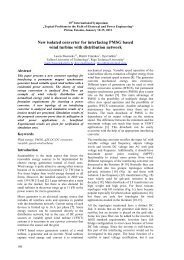
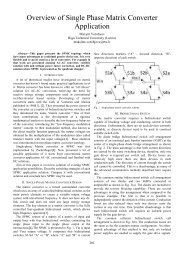
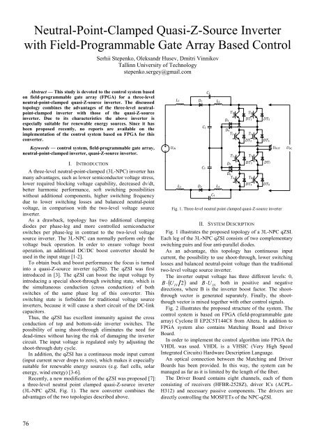
<strong>Neutral</strong>-<strong>Point</strong>-<strong>Clamped</strong> <strong>Quasi</strong>-Z-<strong>Source</strong> <strong>Inverter</strong><strong>with</strong> <strong>Field</strong>-Programmable Gate Array Based ControlSerhii Stepenko, Oleksandr Husev, Dmitri VinnikovTallinn University of Technologystepenko.sergey@gmail.comAbstract — This study is devoted to the control system basedon field-programmable gate array (FPGA) for a three-levelneutral-point-clamped quasi-Z-source inverter. The discussedtopology combines the advantages of the three-level neutralpoint-clampedinverter <strong>with</strong> those of the quasi-Z-sourceinverter. Due to its characteristics the above inverter isespecially suitable for renewable energy sources. Since it hasbeen proposed recently, no reports are available on theimplementation of the control system based on FPGA for thisconverter.L1D1C2C1L2T1D3D4T2T5DT1T6DT2DT5DT6Keywords — control system, field-programmable gate array,neutral-point-clamped inverter, quasi-Z-source inverter.UINT3T7UOUTUDCI. INTRODUCTIONA three-level neutral-point-clamped (3L-NPC) inverter hasmany advantages, such as lower semiconductor voltage stress,lower required blocking voltage capability, decreased dv/dt,better harmonic performance, soft switching possibilities<strong>with</strong>out additional components, higher switching frequencydue to lower switching losses and balanced neutral-pointvoltage, in comparison <strong>with</strong> the two-level voltage sourceinverter.As a drawback, topology has two additional clampingdiodes per phase-leg and more controlled semiconductorswitches per phase-leg in contrast to the two-level voltagesource inverter. The 3L-NPC can normally perform only thevoltage buck operation. In order to ensure voltage boostoperation, an additional DC/DC boost converter should beused in the input stage [1-2].To obtain buck and boost performance the focus is turnedinto a quasi-Z-source inverter (qZSI). The qZSI was firstintroduced in [3]. The qZSI can boost the input voltage byintroducing a special shoot-through switching state, which isthe simultaneous conduction (cross conduction) of bothswitches of the same phase leg of this converter. Thisswitching state is forbidden for traditional voltage sourceinverters, because it will cause a short circuit of the DC-linkcapacitors.Thus, the qZSI has excellent immunity against the crossconduction of top and bottom-side inverter switches. Thepossibility of using shoot-through eliminates the need fordead-times <strong>with</strong>out having the risk of damaging the invertercircuit. The input voltage is regulated only by adjusting theshoot-through duty cycle.In addition, the qZSI has a continuous mode input current(input current never drops to zero), which makes it especiallysuitable for renewable energy sources (e.g. fuel cells, solarenergy, wind energy) [3-6].Recently, a new modification of the qZSI was proposed [7]:a three-level neutral point clamped quasi-Z-source inverter(3L-NPC qZSI, Fig. 1). The new converter combines theadvantages of the two topologies described above.L3D2C3C4L4D5D6T4DT3T8DT4DT7DT8Fig. 1. Three-level neutral point clamped quasi-Z-source inverterII. SYSTEM DESCRIPTIONFig. 1 illustrates the proposed topology of a 3L-NPC qZSI.Each leg of the 3L-NPC qZSI consists of two complementaryswitching pairs and four anti-parallel diodes.As an advantage, this topology has continuous inputcurrent, the possibility to use shoot-through, lower switchinglosses and balanced neutral-point voltage than the traditionaltwo-level voltage source inverter.The inverter output voltage has three different levels: 0,( 2)B ⋅ U INand B ⋅ U both in positive and negativeINdirections, where B is the inverter boost factor. The shootthroughvector is generated separately. Finally, the shootthoughvector is mixed together <strong>with</strong> other control signals.Fig. 2 illustrates the proposed structure of the system. Thecontrol system is based on FPGA (field-programmable gatearray) Cyclone II EP2C5T144C8 from Altera. In addition toFPGA system also contains Matching Board and DriverBoard.In order to implement the control algorithm into FPGA theVHDL was used. VHDL is a VHSIC (Very High SpeedIntegrated Circuits) Hardware Description Language.An optical connection between the Matching and DriverBoards has been provided. In this way, the system can bemanaged as far as it is limited by the length of the fiber.The Driver Board contains eight channels, each of themconsisting of receivers (HFBR-2528Z), driver ICs (ACPL-H312) and necessary passive components. The drivers aredirectly controlling the MOSFETs of the NPC-qZSI.76
The output voltage from the NPC-qZSI is connected to thepower grid through the output filter.MatchingBoardDriverBoardNPC-qZSIIn both of the figures only the gate signals of the switchesT1, T2, T5, T6 have been presented because the aboveswitches have the complementary state <strong>with</strong> the others,respectively (T3, T4, T7, T8).The output voltage of the NPC qZSI controlled by FPGA isshown in Fig. 4.FPGALoadOutputFilterFig. 2. The structure of the proposed systemIII. EXPERIMENTAL RESULTSThe signals applied to the gates of the power converterswitches in the case <strong>with</strong>out the shoot-through state areshown in Fig. 3, a). The signals applied to the gates of powerconverter switches when the shoot-through state was used areshown in Fig. 3, b).Fig. 4. The output voltage of the 3L-NPC qZSI after and beforethe output filterIV. CONCLUSIONSThe control system for a three-level neutral point clampedquasi-Z-source inverter based on the FPGA Cyclone IIEP2C5T144C8 was described. This system allows differentPWM signals to be obtained for different power switches andthe necessary boost factor to be achieved using shoot-throughsignals. The results of the experimental investigations both<strong>with</strong> and <strong>with</strong>out shoot-through states have proved the FPGAbasedcontrol system to be suitable for the 3L-NPC qZSI.ACKNOWLEDGMENTAuthors wish to thank for their support Estonian Ministryof Education and Research (Project SF0140016s11), EstonianScience Foundation (Grants ETF8538 and ETF8687) andEstonian Archimedes Foundation (Project ”Doctoral Schoolof Energy and Geotechnology II“).REFERENCESFig. 3. The control signals applied to the gates of switches <strong>with</strong>out (a) and<strong>with</strong> (b) the shoot-through state[1] F. Gao, P. C. Loh, F. Blaabjerg, D. M. Vilathgamuwa, “Dual Z-sourceinverter <strong>with</strong> three-level reduced common-mode switching,” IEEETransactions on Industry Applications, vol.43, no. 6, pp.1597-1608,2007.[2] P. C. Loh, S. W. Lim, F. Gao, F. Blaabjerg, “Three-level Z-sourceinverters using a single LC impedance network,” IEEE Transactions onPower Electronics, vol. 22, no. 2, pp. 706-711, 2007.[3] J. Anderson, F. Z. Peng, "Four quasi-Z-<strong>Source</strong> inverters," in Proc. ofIEEE Power Electronics Specialists Conference PESC’2008,pp. 2743-2749, June 15-19, 2008.[4] F. Z. Peng, “Z-<strong>Source</strong> inverter,” IEEE Transactions on IndustryApplications, vol. 39, no. 2, pp.504-510, 2003.[5] R. Strzelecki, D. Vinnikov, “Models of the qZ-converters,” PrzegladElektrotechniczny, vol. 86(6), pp. 80 – 84, 2010.[6] P. C. Loh, D. M. Vilathgamuwa, Y. S. Lai, G. T. Chua, Y. W. Li,“Pulse width modulation of Z-<strong>Source</strong> inverter,” IEEE Transactions onPower Electronics, vol. 20, pp. 1346-1355, 2005.[7] S. Ott, I. Roasto, D. Vinnikov, "<strong>Neutral</strong> point clamped quasiimpedance-sourceinverter," in Proc. of Compatibility and PowerElectronics (CPE), 7th International Conference-Workshop,pp. 348-353, June 1-3, 2011..77