Solderball Pin Interconnects - Autosplice Inc.
Solderball Pin Interconnects - Autosplice Inc.
Solderball Pin Interconnects - Autosplice Inc.
- No tags were found...

You also want an ePaper? Increase the reach of your titles
YUMPU automatically turns print PDFs into web optimized ePapers that Google loves.
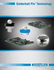
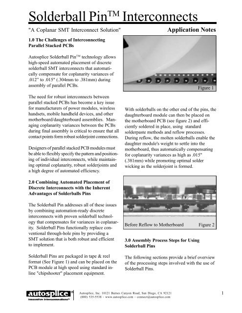
<strong>Solderball</strong> <strong>Pin</strong> TM <strong>Interconnects</strong>"A Coplanar SMT Interconnect Solution" Application Notes1.0 The Challenges of InterconnectingParallel Stacked PCBs<strong>Autosplice</strong> <strong>Solderball</strong> <strong>Pin</strong> TM technology allowshigh-speed automated placement of discretesolderball SMT interconnects that automaticallycompensate for coplanarity variances of.012” to .015" (.304mm to .381mm) duringassembly of parallel PCBs.The need for robust interconnects betweenparallel stacked PCBs has become a key issuefor manufacturers of power modules, wirelesshandsets, mobile handheld devices, and othermotherboard/daughterboard assemblies. Managingcoplanarity variances between the PCBsduring final assembly is critical to ensure that allcontact points form robust solderjoint connections.Designers of parallel stacked PCB modules mustbe able to flexibly specify the pattern and positioningof individual interconnects, while maintainingoptimal coplanarity, robust solderjoints anda high degree of automated efficiency.Figure 1With solderballs on the other end of the pins, thedaughterboard module can then be placed onthe motherboard PCB (see figure 2) and efficientlysoldered in place, using standardsolderpaste methods and reflow processes.During reflow, the molten solderballs enable thedaughter module's weight to settle into themotherboard, thus automatically compensatingfor coplanarity variances as high as .015"(.381mm) while promoting optimal solderwicking as the solderjoint is formed.2.0 Combining Automated Placement ofDiscrete <strong>Interconnects</strong> with the InherentAdvantages of <strong>Solderball</strong>s <strong>Pin</strong>sThe <strong>Solderball</strong> <strong>Pin</strong> addresses all of these issuesby combining automation-ready discreteinterconnects with proven solderball technologythat compensates for variances in coplanarity.<strong>Solderball</strong> <strong>Pin</strong>s functionally replace conventionalthrough-hole pins by providing aSMT solution that is both robust and efficientto implement.<strong>Solderball</strong> <strong>Pin</strong>s are packaged in tape & reelformat (See Figure 1) and can be placed on thePCB module at high speed using standard inline"chipshooter" placement equipment.Before Reflow to Motherboard3.0 Assembly Process Steps for Using<strong>Solderball</strong> <strong>Pin</strong>sFigure 2The following sections provide a brief overviewof the processing steps involved with the use of<strong>Solderball</strong> <strong>Pin</strong>s.<strong>Autosplice</strong>, <strong>Inc</strong>. 10121 Barnes Canyon Road, San Diego, CA 92121(800) 535-5538 - www.autosplice.com - connect@autosplice.com1
3.1 Same Module Designs Can Be Used withEither SMT or Through Hole<strong>Solderball</strong> <strong>Pin</strong> technology enables the samebasic module designs that are used withthrough-hole interconnects to be smoothlytransitioned to SMT processes.The assembly process for a double-sidedthrough-hole module (See Figure 3) typicallyrequires the following steps:• Paste - Place SMT Devices - Reflow• <strong>Pin</strong> Insertion• Flip• Paste - Place SMT Devices - ReflowFigure 3Using <strong>Solderball</strong> <strong>Pin</strong> technology completelyeliminates the pin insertion step, along with theneed for specialized pin insertion equipment.The assembly process for a double-sided SMTnow would require the following steps:• Paste - Place (SMT devices and<strong>Solderball</strong> <strong>Pin</strong>s) - Reflow• Flip• Paste - Place SMT Devices - ReflowThe result is a complete SMT module (SeeFigure 4) with <strong>Solderball</strong> <strong>Pin</strong> SMT interconnects,based on the existing through-hole design.At the end of this step, the PCB module isready for final assembly or, if it is being sold as acommercial component, it is ready for packagingand shipment to end customers for finalassembly into their products.Figure 43.2 Assembly of the Daughter Module to theSecond PCB or MotherboardThe <strong>Solderball</strong> <strong>Pin</strong> design allows the completedPCB module to be efficiently placed into paste onthe second parallel stacked PCB (ormotherboard assembly) and processed alongwith all other SMT components, using standardreflow operations.The completed PCB module can be placed directlyinto solderpaste on the motherboard withexisting SMT pick and place systems andstandard process technologies (See Figure 5).Figure 5Because the <strong>Solderball</strong> <strong>Pin</strong> is designed to optimize efficient solder wicking and robustsolderjoint formation, daughter modules can beplaced directly into standard amounts ofsolderpaste on the motherboard, without necessitatingany specialized secondary processes.2 <strong>Autosplice</strong>, <strong>Inc</strong>. 10121 Barnes Canyon Road, San Diego, CA 92121(800) 535-5538 - www.autosplice.com - connect@autosplice.com
<strong>Autosplice</strong>, <strong>Inc</strong>. 10121 Barnes Canyon Road, San Diego, CA 92121(800) 535-5538 - www.autosplice.com - connect@autosplice.com3
3.3 Coplanarity-Compensation During FinalAssembly Reflow Solder Process<strong>Solderball</strong> <strong>Pin</strong>s are designed to provide automaticcoplanarity compensation, while maintainingcompatibility with most standard SMTprocesses. During reflow, each <strong>Solderball</strong> <strong>Pin</strong>provides adjustment flexibility that is equal tothe distance by which the diameter of thesolderball extends beyond the end of the pininside the ball. (See Figure 6) The internal pinprovides a rigid and high-conductivity foundationand the reflow of the solderball allows aphysical adjustment up to .015" (.381mm) aseach solderjoint is formed.When the solderballs "go liquidus" duringreflow the molten solder wicks and adheres toboth the copper pin and the landing pad, forminga robust solderjoint. Because the weight ofthe daughter module is greater than the buoyancyof the molten solder, the unit is able tosettle to the standoff height “D” on to themotherboard during reflow, thus compensatingfor variances in coplanarity between the PCBs.This ability to automatically adjust for coplanarityvariances during reflow means that the manufacturergains a significant amount of "latitudein the process window" because all ofthe contacts do not have to be perfectly seatedduring the initial placement. For example, atypical module might have between 6 and 12discrete interconnect points, of which severalpoints could be slightly up off of the pads andwould still be brought into compliance as themodule sinks towards the motherboard duringreflow.Each <strong>Solderball</strong> <strong>Pin</strong> is designed with an integratedblack insulator collar (See Figure 7) thatprevents solder from flowing all the way up theshaft of the pin during reflow, thus assuring thatthe flow instead forms a consistent solderjointwith the target pad on the underlying PCB.This also promotes efficient use of the availableFigure 6solder, thus allowing for optimal results withstandard solderpaste levels.When compared to other alternatives for creatingmodule-level SMT connections, such as floatingcontacts, post-forming of flex pins, or complexcladding methods, <strong>Solderball</strong> <strong>Pin</strong>s provide anFigure 74 <strong>Autosplice</strong>, <strong>Inc</strong>. 10121 Barnes Canyon Road, San Diego, CA 92121(800) 535-5538 - www.autosplice.com - connect@autosplice.com
inherently simple approach that leveragesexisting automation techniques as well asflexibility and autocompensation advantages ofsolderball technology.4.0 <strong>Solderball</strong> <strong>Pin</strong>s are Designed forEfficient High-speed Pick and Place<strong>Solderball</strong> <strong>Pin</strong>s are packaged in EIA standard tape& reel format and are designed for placement onhigh-speed "chipshooter" equipment, without anyrequirement for specialized feeders or placementplatforms.The insulator collar on each pin acts a mating pointfor the placement machine's vacuum pick-up headto assure consistent alignment during placement ofthe pins on to the first PCB. Instead of having thevacuum head attempt to pick-up the roundedsurface of the solderball and run the risk ofcanting the alignment, the system is designed forthe nozzle to slip completely over the solderballand acquire the uniformly flat surface of thecollar. (See Figure 8)4.1 Vision System SettingsBased on the lighting type utilized (Back-lit orFront-lit) the vision system should be set up to lookat different areas of the <strong>Solderball</strong> <strong>Pin</strong>. (SeeFigure 8)4.1.1 Back-LitWhen using a back-lit system the vision systemwill be looking for the black insulator. It thenbecomes important that insulator hides thenozzle so that the vision system doesn't mistakethe nozzle for the component. Therefore therelationship of the ID of the nozzle to thesolderball and the OD of the nozzle to theinsulator is important. (See Figure 8) Thenozzle selected should have an inside diameter(ID) that is between .177mm to .254mm largerthan the solderball on the pin. It is recommendedthat the nozzle’s OD be a maximum of.254mm smaller than the insulator’s diameter.4.1.2 Front Lit Vision SystemFigure 8A front-lit system the vision system should beable to differentiate between the silver colorflange on the pin and the black insulator. Thiswill allow the vision system to use the flange ofthe pin for part alignment. In this case therelationship between the nozzle the solderballand the insulator becomes less important. (SeeFigure 8)4.1.3 Other Vision System Recommendations<strong>Autosplice</strong>, <strong>Inc</strong>. 10121 Barnes Canyon Road, San Diego, CA 92121(800) 535-5538 - www.autosplice.com - connect@autosplice.com5
4.2 Picking the <strong>Solderball</strong>Because the nozzle pick plane is the insulator,the pick up depth for the nozzle from the topsurface of the pocket tape should be approximately.020” (.7mm) (See figure 9).4.3 Placing the <strong>Solderball</strong>Since the leg of the <strong>Solderball</strong> <strong>Pin</strong> is taperedfrom the flange, the machine should be set upduring the placement cycle for an over travel ofapproximately .012” (.3mm) from the surface ofthe PCB. This will guarantee that the part isseated properly and that the flange is in contactwith the paste. The component library shouldindicate the component thickness as the dimensionbetween the flange and the insulator. Notethat the measurement for over travel is from the<strong>Solderball</strong> <strong>Pin</strong>'s flange to the surface of the PCB.(See Figure 9 for details).Figure 95.0 <strong>Solderball</strong> <strong>Pin</strong> Specifications, Configurations,OptionsInitially, <strong>Solderball</strong> <strong>Pin</strong>s are available in thefollowing configurations:• Available solderball diameters of .062"(1.57) (standard) with options for .055"(1.4) or .031" (.787) (low profile).• <strong>Pin</strong> diameters of .040" (1.0) or .062" (1.57)• <strong>Solderball</strong>s initially consist of 63/37 EutecticSolder - with future options for leadfreetin/silver/copper balls• All configurations packaged in EIA standardtape & reel• Future designs also could combine the<strong>Solderball</strong> <strong>Pin</strong> with <strong>Autosplice</strong>'s TreadHeadSMT technology to provide a pure SMTto-SMTinterconnect solution.<strong>Solderball</strong> <strong>Pin</strong>'s use of high conductivity copperfor the pin enables the interconnect to conductfrom 30 to 40 Amps in order to meet requirementsacross a full range of today's powerdevice applications.<strong>Solderball</strong> <strong>Pin</strong>s are available to fit in the twomost prevalent PCB hole diameters that arecurrently used in the power industry - .040"(1mm) and .062" (1.5mm) pin terminals. Thisgives manufacturers optimal flexibility for usingthe same core production processes to createeither conventional modules with through-holepins or surface mount modules using <strong>Solderball</strong><strong>Pin</strong>s.The standard solderball diameter of .062" (1.57)is designed to accommodate the majority ofapplications, however production options forsolderball diameters of .055" (1.4) or .031"(.787) also allow for low-profile applicationsand smaller placement centers, in which theamount of solder under the device must belimited.The basic <strong>Solderball</strong> <strong>Pin</strong> technology also allows forthe creation of custom pin diameters and/or pinlengths to meet specific customer requirements.For example, pin lengths can be custom tailored forspecific inter-PCB standoff distances to accommodatevarious component heights on themotherboard. (Use the enclosed <strong>Solderball</strong> <strong>Pin</strong>design guide to help <strong>Autosplice</strong> to define thebest part for your application.)6 <strong>Autosplice</strong>, <strong>Inc</strong>. 10121 Barnes Canyon Road, San Diego, CA 92121(800) 535-5538 - www.autosplice.com - connect@autosplice.com
6.0 Benefits Summary• Packaged in 16mm EIA standard tapeand reel• Automatically compensates for coplanarity.• Provide enough solder volume to createa robust SMT interconnect.• Fits into existing through-holes onmodule saving real estate• Allows for seamless conversions fromSMT to through-hole designs<strong>Autosplice</strong>, <strong>Inc</strong>. 10121 Barnes Canyon Road, San Diego, CA 92121(800) 535-5538 - www.autosplice.com - connect@autosplice.com7
8 <strong>Autosplice</strong>, <strong>Inc</strong>. 10121 Barnes Canyon Road, San Diego, CA 92121(800) 535-5538 - www.autosplice.com - connect@autosplice.com