

1989-04
1989-04
1989-04
- No tags were found...

You also want an ePaper? Increase the reach of your titles
YUMPU automatically turns print PDFs into web optimized ePapers that Google loves.
HEWLETT- PACKARDJ — LJ A P R I L 1 9 B 9H E W L E T TP A C K A R D© Copr. 1949-1998 Hewlett-Packard Co.
cjH E W L E T T -a_i — uApril <strong>1989</strong> Volume 40 • Number 2Articles6 An 81/2-Digit Digital Multimeter Capable of 100,000 Readings per Second and Two-Source Calibration, by Scott D. Stever8 An 81/2-Digit Integrating Analog-to-Digital Converter with 16-Bit, 100,000-Sampleper-SecondPerformance, by Wayne C. GoekeIf- Precision AC Voltage Measurements Using Digital Sampling Techniques, by RonaldO L. Swerleinr\ r\ External of an 81/z-Digit Multimeter from Only Two External Standards, by Wayne¿_¿_ D. Goeke, Ronald L. Swerlein, Stephen B. Venzke, and Scott D. Stever24 Josephson Junction Arrays28 A High-Stability Voltage ReferenceO H Design for High Throughput in a System Digital Multimeter, by Gary A. Ceely andO I David J. Rustid33 Firmware Development System36 Custom UART Design39High-Resolution Digitizing Techniques with an Integrating Digital Multimeter, byDavid A. Czenkusch42 Time Interpolation46 Measurement of Capacitor Dissipation Factor Using Digitizing5057A Structural Approach to Software Defect Analysis, by Takeshi Nakajo, KatsuhikoSasabuchi, and Tadashi AkiyamaDissecting Software Failures, by Robert B. Grady62 Defect Origins and TypesEditor, Richard P. Dolan • Associate Editor, Charles L. Leath • Assistant Editor, Hans A. Toepfer • Art Director, Photographer, Arvid A. DanielsonSupport European Susan E, Wright • Administrative Services, Typography, Anne S. LoPresti • European Production Supervisor, Michael Zandwijken2 HEWLETT-PACKARD JOURNAL APRIL <strong>1989</strong> © Hewlett-Packard Company <strong>1989</strong> Printed in U.S.A.© Copr. 1949-1998 Hewlett-Packard Co.
Çï A Software Defect Prevention Using McCabe's Complexity Metric, by William T. Ward6966 The Cyclomatic Complexity MetricObject-Oriented Unit Testing, by Steven P. Fiedler75Validation and Further Application of Software Reliability Growth Models, by GregoryA. Kruger80869196Comparing Structured and Unstructured Methodologies in Firmware Development,by William A. Fischer, Jr. and James W. JostAn Object-Oriented Methodology for Systems Analysis and Specification, by BarryD. Kurtz, Donna Ho, and Teresa A. WallVXIbus: A New Interconnection Standard for Modular Instruments, by KennethJessenVXIbus Product Development Tools, by Kenneth JessenDepartments4 In this Issue5 Cover5 What's Ahead56 Corrections98 AuthorsThe Hewlett-Packard Journal is published bimonthly by the Hewlett-Packard Company to recognize technical contributions made by Hewlett-Packard (HP) personnel. Whilethe information of in this publication is believed to be accurate, the Hewlett-Packard Company makes no warranties, express or implied, as to the accuracy or reliability ofsuch information. The Hewlett-Packard Company disclaims ail warranties of merchantability and fitness for a particular purpose and all obligations and liabilities for damages,including but not limited to indirect, special, or consequential damages, attorney's and expert's fees, and court costs, arising out of or in connection with this publication.Subscriptions: non-HP Hewlett-Packard Journal is distributed free of charge to HP research, design, and manufacturing engineering personnel, as well as to qualified non-HPindividuals, business and educational institutions. Please address subscription or change of address requests on printed letterhead (or include a business card) to the HP addresson the please cover that is closest to you. When submitting a change of address, please include your zip or postal code and a copy of your old label.Submissions: research articles in the Hewlett-Packard Journal are primarily authored by HP employees, articles from non-HP authors dealing with HP-related research orsolutions contact technical problems made possible by using HP equipment are also considered for publication. Please contact the Editor before submitting such articles. Also, theHewlett-Packard should encourages technical discussions of the topics presented in recent articles and may publish letters expected to be of interest to readers. Letters shouldbe brief, and are subject to editing by HP.Copyright publication that 989 Hewlett-Packard Company. All rights reserved. Permission to copy without fee all or part of this publication is hereby granted provided that 1 ) the copiesare not Hewlett-Packard used, displayed, or distributed for commercial advantage; 2) the Hewlett-Packard Company copyright notice and the title of the publication and date appear on:he copies; Otherwise, be a notice stating that the copying is by permission of the Hewlett-Packard Company appears on the copies. Otherwise, no portion of this publication may beproduced recording, information in any form or by any means, electronic or mechanical, including photocopying, recording, or by any information storage retrieval system without writtenpermission of the Hewlett-Packard Company.Please Journal, inquiries, submissions, and requests to: Editor, Hewlett-Packard Journal, 3200 Hillview Avenue, Palo Alto, CA 943<strong>04</strong>, U.S.A.APRIL <strong>1989</strong> HEWLETT-PACKARD JOURNAL 3© Copr. 1949-1998 Hewlett-Packard Co.
In this IssueIf you thought that voltmeters, those ancient and fundamental instruments,had evolved about as far as possible and that there couldn't be much moreto say digital them, you'd be wrong. Today, they're usually called digitalmultimeters or DMMs rather than voltmeters. You can find highly accurate•>,• automated ones in calibration laboratories, very fast ones in automated test systems,ijf VHBI m and a whole spectrum of performance levels and applications in betweenII these extremes. Generally, more speed means less resolution — that is, fewer~JJ^^^^¿2 digits in the measurement result. Conversely, a higher-resolution measure-HM ^mmamÈ I ment generally takes longer. Some DMMs are capable of a range of speedsand resolutions and allow the user to trade one for the other. The HP 3458A Digital Multimeterdoes this to an unprecedented degree. It can make 100,000 41/2-digit measurements per secondor six continuous measurements per second, and allows the user an almost continuous selectionof speed-versus-resolution trade-offs between these limits. You'll find an introduction to the HP3458A on page 6. The basis of its performance is a state-of-the-art integrating analog-to-digitalconverter (ADC) that uses both multislope runup and multislope rundown along with a two-inputstructure to achieve both high speed and high precision (page 8). So precise is this ADC that itcan function as a ratio transfer device for calibration purposes. With the ADC and a trio of built-intransfer only all of the functions and ranges of the HP 3458A can be calibrated using onlytwo external traceable standards — 10V and 10 kil. The article on page 22 explains how this ispossible. At the high end of its speed range, the ADC allows the HP 3458A to function as ahigh-speed digitizer, an unusual role for a DMM (page 39). In fact, ac voltage measurements aremade eliminating analog the input signal and computing its rms value, eliminating the analog rms-to-dcconverters of older designs (page 15). Finally, moving data fast enough to keep up with the ADCwas a design challenge in itself. How it was met with a combination of high-speed circuits andefficient firmware is detailed in the article on page 31 .The seven papers on pages 50 to 90 are from the 1988 HP Software Engineering ProductivityConference and should be of interest to software engineers and users concerned with softwaredefect prevention. Collectively, the papers spotlight areas where vigorous software engineeringactivity testing, occurring today, namely in structured and object-oriented analysis, design, and testing,and in the paper of reliable metrics with which to measure software quality. ^ In the paperon page describe engineers from Yokogawa Hewlett-Packard and Tokyo University describe a jointeffort to find the flaws in design procedures that increase the likelihood of human errors that resultin program faults. Working backwards from faults to human errors to flawed procedures, theypropose various structured analysis and design solutions to eliminate the flaws. > The paper onpage 57 project expansion of the software defect data collection process so that project managerscan not only determine how best to prevent future defects, but also build a case for making thenecessary changes in procedures. The time required to collect and analyze the additional datais shown to be minimal. ^ That complexity leads to defects is well-established, so monitoring thecomplexity of software modules during implementation should point out modules that will be defectprone. The paper on page 64 tells how HP's Waltham Division is taking this approach to improvethe software development process, using McCabe's cyclomatic complexity metric to measurecomplexity. ^ Object-oriented programming, originally conceived for artificial intelligence applications, and now finding wider acceptance. The paper on page 69 reports on problems and methodsassociated with testing software modules developed with an object-oriented language, C + + , fora clinical information system. > In the paper on page 75, Greg Kruger updates his June 1988paper on the use of a software reliability growth model at HP's Lake Stevens Instrument Division.4 HEWLETT-PACKARD JOURNAL APRIL <strong>1989</strong>© Copr. 1949-1998 Hewlett-Packard Co.
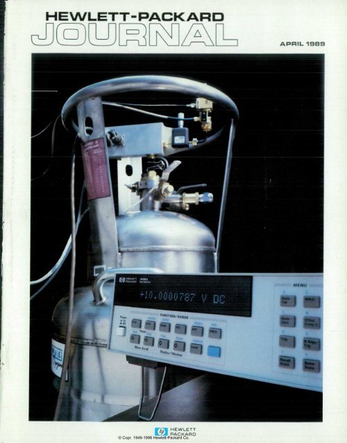
The model it. generally been successful, but there are pitfalls to be avoided in applying it. >On a software project at HP's Logic Systems Division, some of the engineers used structuredmethods the some used unstructured methods. Was structured design better? According to thepaper offered page 80, the results were mixed, but the structured methods offered enough benefitsto justify their continued use. *• In software development, system analysis precedes design. Thepaper on increas 86 describes a new object-oriented approach suitable for analyzing today's increasingly based and more complex systems. The authors believe that designs based on object-orientedspecifications can be procedure-oriented or object-oriented with equal success.Modular measurement systems consist of instruments on cards that plug into a card cage ormainframe. A user can tailor a system to an application by plugging the right modules into themainframe. The VXIbus is a new industry standard for such systems. Modules and mainframesconforming to the VXIbus standard are compatible no matter what company manufactured them.The articles on pages 91 and 96 introduce the VXIbus and some new HP products that helpmanufacturers develop VXIbus modules more quickly. HP's own modular measurement systemarchitecture conforms to the VXIbus standard where applicable. However, for high-performanceRF and system instrumentation, HP has used a proprietary modular system interface bus(HP-MSIB). Patent rights to the HP-MSIB have now been assigned to the public so that thisarchitecture can be used by everyone as the high-frequency counterpart of the VXIbus.P.P. DolanEditorCoverSo precise is the 3458A Digital Multimeter that verifying some aspects of its performance isbeyond Division limits of conventional standards. In the HP Loveland Instrument Division StandardsLaboratory, the HP 3458A's linearity is measured using a 10-volt Josephson junction array developed by the U.S. National Institute of Standards and Technology. The array is in a speciallymagnetically shielded cryoprobe in the center of a liquid-helium-filled dewar (the tank with theprotective "steering wheel.") On top of the dewar are a Gunn-diode signal source (72 GHz) andvarious to components. A waveguide and voltage and sense leads connect the array tothe external components. For more details see page 24.What's AheadSubjects to be covered in the June issue include:• The Architecture 9000 Model 835 and HP 3000 Series 935 Midrange HP Precision ArchitectureComputers• Programming with neurons• A new 2D simulation model for electromigration in thin metal films• Data compression and blocking in the HP 7980XC Tape Drive• Design and applications of HP 8702A Lightwave Component Analyzer systems• A data base for real-time applications and environments• A hardware/software tool to automate testing of software for the HP Vectra PersonalComputer.© Copr. 1949-1998 Hewlett-Packard Co.APRIL <strong>1989</strong> HEWLETT-PACKARD JOURNAL 5
An 81/2-Digit Digital Multimeter Capable of100,000 Readings per Second andTwo-Source CalibrationA highly linear and extremely flexible analog-to-digitalconverter and a state-of-the-art design give this DM M newperformance and measurement capabilities for automatedtest, calibration laboratory, or R&D applications.by Scott D. SteverTHE DIGITAL MULTIMETER OR DMM is among themost common and most versatile instruments available for low-frequency and dc measurements in automated test, calibration laboratory, and bench R&D applications. The use of general-purpose instrumentation in automated measurement systems has steadily grown over thepast decade. While early users of programmable instruments were elated to be able to automate costly, tedious,error-prone measurements or characterization processes,the sophistication and needs of today's users are orders ofmagnitude greater. The computing power of instrumentcontrollers has increased manyfold since the mid-1970sand so have user expectations for the performance of measurement systems. Test efficiency in many applications isno longer limited by the device under test or the instrumentcontroller's horsepower. Often either the configurationspeed or the measurement speed of the test instrumentationhas become the limiting factor for achieving greater testthroughput. In many systems, the DMM is required to perform hundreds of measurements and be capable of multiplefunctions with various resolutions and accuracies.In some applications, several DMMs may be required tocharacterize a single device. For example, measurementsrequiring high precision may need a slower DMM withcalibration laboratory performance. Usually, the majorityof measurements can be satisfied by the faster, moderateresolutioncapabilities of a traditional system DMM. In extreme cases, where speed or sample timing are critical tothe application, a lower-resolution high-speed DMM maybe required. A single digital multimeter capable of fulfillingthis broad range of measurement capabilities can reducesystem complexity and development costs. If it also provides shorter reconfiguration time and increased measurement speed, test throughput can also be improved for automated test applications.The HP 3458A Digital Multimeter (Fig. 1) was developedto address the increasing requirements for flexible, accurate, and cost-effective solutions in today's automated testapplications. The product concept centers upon the synergisticapplication of state-of-the-art technologies to meetthese needs. While it is tuned for high throughput in computer-aided testing, the HP 3458A also offers calibrationlaboratory accuracy in dc volts, ac volts, and resistance.Owners can trade speed for resolution, from 100,000 measurements per second with 4V2-digit (16-bit) resolution tosix measurements per second with 8V2-digit resolution. At5V2-digit resolution, the DMM achieves 50,000 readingsper second. To maximize the measurement speed for theresolution selected, the integration time is selectable from500 nanoseconds to one second in 100-ns steps. The effectis an almost continuous range of speed-versus-resolutiontrade-offs.Fig. 1 . The HP 3458 A Digital Multimeter can make 700,000 41/2-digit readings per second for highspeed automated test applications. For calibration laboratoryapplications, it can make six 8V?-d/git readings per second. Finecontrol of the integration aperturea/lows a nearly continuous rangeof speed-versus-resoultion tradeoffs.6 HEWLETT-PACKARD JOURNAL APRIL <strong>1989</strong>© Copr. 1949-1998 Hewlett-Packard Co.
Measurement CapabilitiesMeasurement ranges for the HP 3458A's functions are:• Voltage: 10 nV to 1000V dc
An 81/2-Digit Integrating Analog-to-DigitalConverter with 16-Bit, 100,000-Sample-per-Second PerformanceThis integrating-type ADC uses multislope runup,multislope rundown, and a two-input structure to achievethe required speed, resolution, and linearity.by Wayne C. GoekeTHE ANALOG-TO-DIGITAL CONVERTER (ADC)design for the HP 3458A Digital Multimeter was driven by the state-of-the-art requirements for the systemdesign. For example, autocalibration required an ADC withSVz-digit (28-bit] resolution and 7V2-digit (25-bit) integrallinearity, and the digital ac technique (see article, page 22)required an ADC capable of making 50,000 readings persecond with 18-bit resolution.Integrating ADCs have always been known for their ability to make high-resolution measurements, but tend to berelatively slow. When the HP 3458A's design was started,the fastest integrating ADC known was in the HP 3456ADMM. This ADC uses a technique known as multislopeand is capable of making 330 readings per second. The HP3458A's ADC uses an enhanced implementation of thesame multislope technique to achieve a range of speedsand resolutions never before achieved — from 16-bit resolution at 100,000 readings per second to 28-bit resolution atsix readings per second. In addition to high resolution, theADC has high integral linearity — deviations are less than0.1 ppm (parts per million) of input.Multislope is a versatile ADC technique, allowing speedto be traded off for resolution within a single circuit. It iseasier to understand multislope by first understanding itspredecessor, dual-slope.V0(tu) = -(l/RC)Vintu.Next a known reference voltage Vref with polarity opposite to that of Vin is connected to the same resistor R byclosing SW2. A counter is started at this time and is stoppedwhen the output of the integrator crosses through zero volts.This portion of the algorithm is known as rundown. Thecounter contents can be shown to be proportional to theunknown input.V0(t2) = V0(tu) - (l/RC)Vreftd = 0,where td is the time required to complete rundown (i.e.,td = t2 - tj. Solving for Vin,vin=-vref(td/tj.Letting Nu be the number of clock periods (Tck) duringVinOSW1Basic Dual-Slope TheoryDual-slope is a simple integrating-type ADC algorithm.Fig. 1 shows a simple circuit for implementing a dual-slopeADC.The algorithm starts with the integrator at zero volts.(This is achieved by shorting the integrator capacitor, C.)At time 0 the unknown input voltage Vin is applied to theresistor R by closing switch SWl for a fixed length of timetu. This portion of the algorithm, in which the unknowninput is being integrated, is known as runup. At the endof runup (i.e., when SWl is opened), the output of theintegrator, V0, can be shown to beVretTimeV0(tJ = -(1/RC) P"vin(t)dtJoRunupRundownor, when Vin is time invariant,Fig. 1. Dual-slope integrating ADC (analog-to-digital converter) circuit and a typical waveform.8 HEWLETT-PACKARD JOURNAL APRIL <strong>1989</strong>© Copr. 1949-1998 Hewlett-Packard Co.
unup and Nd the number of clock periods during rundown,time cancels andVin = - Vref{Nd/Nu).The beauty of the dual-slope ADC technique is its insensitivityto the value of most of the circuit parameters. Thevalues of R, C, and Tck all cancel from the final equation.Another advantage of the dual-slope ADC is that a singlecircuit can be designed to trade speed for resolution. If therunup time is shortened, the resolution will be reduced,but so will the time required to make the measurement.The problem with the dual-slope algorithm is that itsresolution and speed are limited. The time Tm for a dualslopeADC to make a measurement is determined by:Tm = 2TckM,where Tm is the minimum theoretical time to make a fullscalemeasurement, Tck is the period of the ADC clock, andM is the number of counts of resolution in a full-scalemeasurement. Even with a clock frequency of 20 MHz, tomeasure a signal with a resolution of 10,000 counts requiresat least 1 millisecond.The resolution of the dual-slope ADC is limited by thewideband circuit noise and the maximum voltage swingof the integrator, about ±10 volts. The wideband circuitnoise limits how precisely the zero crossing can be determined. Determining the zero crossing to much better thana millivolt becomes very difficult. Thus, dual-slope is limited in a practical sense to four or five digits of resolution(i.e., 10V/1 mV).Enhanced Dual-SlopeThe speed of the dual-slope ADC can be nearly doubledsimply by using a pair of resistors, one for runup and theother for rundown, as shown in Fig. 2.The unknown voltage, Vin, is connected to resistor Ru.which is much smaller than resistor Rd, which is usedduring rundown. This allows the runup time to be shortened by the ratio of the two resistors while maintainingthe same resolution during rundown. The cost of the addedspeed is an additional resistor and a sensitivity to the ratioof the two resistors:Vin = - Vref(Nd/NJ(Ru/Rd).Because resistor networks can be produced with excellent ratio tracking characteristics, the enhancement is veryfeasible.Multislope RundownEnhanced dual-slope reduces the time to perform runup.Multislope rundown reduces the time to perform rundown.Instead of using a single resistor (i.e., a single slope) toseek zero, multislope uses several resistors (i.e., multipleslopes) and seeks zero several times, each time more precisely. The ratio of one slope to another is a power of somenumber base, such as base 2 or base 10.Fig. 3 shows a multislope circuit using base 10. Fourslopes are used in this circuit, with weights of 1000, 100,10, and 1. Each slope is given a name denoting its weight+Vrel-VrefTimeRundown+S1000 +S10 -S1-S100Runup RundownFig. 2. Enhanced dual-slope ADC circuit uses two resistors,one lor runup and one for rundown.Fig. 3. Base- W multislope rundown circuit.APRIL <strong>1989</strong> HEWLETT-PACKARD JOURNALS© Copr. 1949-1998 Hewlett-Packard Co.
eyond the limit. The HP 3458A has an effective voltageswing of ±120,000 volts when making 8V2-digit readings,which means the rundown needs to resolve a millivolt toachieve an SVz-digit reading (i.e.. 120.000V 0.001Y =120.000,000 counts).The multislope runup algorithm has two advantages overdual-slope runup: (1) the runup can be continued for anylength of time without saturating the integrator, and (2)resolution can be achieved during runup as well as duringrundown. The HP 3458A resolves the first 4Vi digits duringrunup and the final 4 digits during rundown to achieve anSVz-digit reading.An important requirement for any ADC is that it be linear.With the algorithm described above, multislope runupwould not be linear. This is because each switch transitiontransfers an unpredictable amount of charge into the integrator during the rise and fall times. Fig. 6 shows twowaveforms that should result in the same amount of chargetransferred to the integrator, but because of the differentnumber of switch transitions, do not.This problem can be overcome if each switch is operateda constant number of times for each reading, regardless ofthe input signal. If this is done, the charge transferred during the transitions will result in an offset in all readings.Offsets can be easily removed by applying a zero inputperiodically and subtracting the result from all subsequentreadings. The zero measurement must be repeated periodically because the rise and fall times of the switches driftwith temperature and thus the offset will drift.Multislope runup algorithms can be implemented withconstant numbers of switch transitions by alternately placing an S+0 and an S_0 between each runup slope. Fig. 7shows the four possible slope patterns between any twoS+o slopes. Varying input voltages will cause the algorithmto change between these four patterns, but regardless ofwhich pattern is chosen, each switch makes one and onlyone transition between the first S+0 slope and the S_0 slope,and the opposite transition between the S_0 slope and thesecond S+0 slope.The cost of multislope runup is relatively small. Therunup slopes can have the same weight as the first slopeof multislope rundown. Therefore, only the opposite-polarity slope has to be added, along with the logic to implementthe algorithm.HP 3458A ADC DesignThe design of the HP 3458A's ADC is based on thesetheories for a multislope ADC. Decisions had to be madeon how to control the ADC, what number base to use, howfast the integrator can be slewed and remain linear, howmuch current to force into the integrator (i.e., the size ofthe resistors), and many other questions. The decisionswere affected by both the high-speed goals and the high-resolution goals. For example, very steep slopes are neededto achieve high speed, but steep slopes cause integratorcircuits to behave too nonlinearly for high-resolution measurement performance.One of the easier decisions was to choose a number basefor the ADC's multislope rundown. Base e is the optimumto achieve the highest speed, but the task of accumulatingan answer is difficult, requiring a conversion to binary.Base 2 and base 4 are both well-suited for binary systemsand are close to base e. Base 2 and base 4 are actuallyequally fast, about 6% slower than base e, but base 2 usestwice as many slopes to achieve the same resolution. Therefore, base 4 was chosen to achieve the required speed withminimum hardware cost.Microprocessors have always been used to control multislope ADCs, but the speed goals for the HP 3458A quicklySWbVoSWa7T8TSWbFig. 5. Integrator output waveform for multislope runup. Thedashed line shows the effective integrator output voltageswing.Fig. 6. Ideally, these two waveforms would transfer equalcharge into the integrator, but because of the different numberof switch transitions, they do not.APRIL <strong>1989</strong> HEWLETT-PACKARD JOURNAL 11© Copr. 1949-1998 Hewlett-Packard Co.
SWaSWbSWaSWbS+o S- S-o S + S+oPattern No. 1S+o S+ S-o S- S+oPattern No. 2SWaSWbSWaSWbS+o S- S-o S- S+oPattern No. 3S+o S+ S-o S+ S+oPattern No. 4Fig. 7. Multislope runup patterns for an algorithm that keepsthe number of switch transitions constant.eliminated the possibility of using a microprocessor to control the ADC algorithm. It was anticipated that the ADCclock frequency would have to be between 10 and 20 MHz,and making decisions at these rates requires dedicatedhardware. Therefore, a gate array was chosen to implementstate machines running at 20 MHz for ADC control. TheADC control and accumulator functions consume approximately half of a 6000-gate CMOS gate array. The other halfof the gate array is devoted to the timing and counting oftriggers and a UART (universal asynchronous receiver/transmitter) to transfer data and commands through a 2-Mbit/s fiber optic link to and from the ground-referencedlogic (see article, page 31).The number of slopes and the magnitude of the currentsfor each slope are more subtle decisions. If the slope currents get too large, they stress the output stage of the integrator's operational amplifier, which can cause nonlinearbehavior. If the currents are too small, switch and amplifierleakage currents can become larger than the smallest slopecurrent, and the slope current would not be able to convergethe integrator toward zero. A minimum of a microamperefor the smallest slope was set to avoid leakage current problems. Also, it was believed that the integrator could handleseveral milliamperes of input current and remain linearover five or six digits, but that less than a milliampere ofinput current would be required to achieve linearity overseven or eight digits. On the other hand, greater than amilliampere of current was needed to achieve the highspeed reading rate goal. Therefore, a two-input ADC structure was chosen.As shown in Fig. 8, when making high-speed measurements, the input voltage is applied through a 1 0-kÃà resistor,and the ADC's largest slopes, having currents greater thana milliampere, are used. When making high-resolutionmeasurements, the input voltage is applied through a 50-kflresistor and the largest slopes used have less than a milliampere of current. The largest slope was chosen to be Si 024,having 1.2 /u.A of current. This led to a total of six slopes(S1024, S256, S64, S16, S4, and Si) with Si having about1.2 ¡¿A of current. S1024 and S256 are both used duringmultislope runup; therefore, both polarities exist for bothslopes. The ±8256 slopes (0.3 mA) are used when the50-kohm input is used and both the ±81024 and the ±5256slopes (1.5 mA total) are used in parallel when the 10-kilinput is used. The 8256 slope is 25% stronger than a fullscaleinput to the 50-kfi resistor, which allows it to keepthe integrator from saturating. The 10-kfl input is five times+vref-v,Fig. 8. Simplified HP 3458A ADCcircuit.12 HEWLETT-PACKARD JOURNAL APRIL <strong>1989</strong>© Copr. 1949-1998 Hewlett-Packard Co.
stronger than the 50-kohm input: thus, by using both S1024and S256. 25% stronger reference slopes can be maintainedduring high-speed measurements.IntegratorThe integrator's operational amplifier behaves more nonlinearlyas the integrator slew rate (i.e.. the steepest slope)approaches the slew rate of the amplifier. Two factors determine the integrator slew rate: the total current into theintegrator and the size of the integrator capacitor. Wantingto keep the integrator slew rate less than 10V//u.s led to anintegrator capacitor of 330 pF. This capacitor must have avery small amount of dielectric absorption since 50 fC ofcharge is one count.The integrator circuit has to respond to a change in reference current and settle to near 0.01% before the next possible switch transition (about 200 ns). It also has to havelow voltage and current noise, about IOOV//J.S slew rate, adc gain of at least 25,000, an offset voltage less than 5 mV,and a bias current of less than 10 n A. A custom amplifierdesign was necessary to achieve all the specifications.Resistor NetworkThe resistor network has several requirements. The moststringent is to obtain the lowest ratio-tracking temperaturecoefficient possible. It is important to keep this coefficientlow because the gain of the ADC is dependent on the ratioof the input resistor to the runup reference slope resistors.An overall temperature coefficient of 0.4 ppm/°C wasachieved for the ADC. Even at this level, a temperaturechange of 0.1°C results in a five-count change in a full-scale8V2-digit measurement. (Autocalibration increases the gainstability to greater than 0.15 ppm/°C.)Another requirement for the resistor network is to havea low enough absolute temperature coefficient that nonlinearitiesare not introduced by the self-heating of theresistors. For example, the 50-kil input resistor has a inputvoltage that ranges from +12V to -12V. There is a 2.88-milliwatt power difference between a 0V input and a 12Vinput. If this power difference causes the resistor to changeits value, the result is a nonlinearity in the ADC. A 0.01°Ctemperature change in a resistor that has an absolute temperature coefficient of 1 ppm/°C causes a one-count errorin an SVi-digit measurement. The network used in the HP3458A's ADC shows no measurable self-heating nonlinearities.The final requirement of the resistor network is that itmaintain the ratios of the six slopes throughout the life ofthe HP3458A. The tightest ratio tolerance is approximately0.1% and is required to maintain linearity of the high-speedmeasurements. This is a relatively easy requirement. Tomaintain the ADC's SVz-digit differential linearity at lessthan 0.02 ppm requires ratio tolerances of only 3%.SwitchesA last major concern for the ADC design was the switchesrequired to control the inputs and the slopes. Because theswitches are in series with the resistors, they can add tothe temperature coefficient of the ADC. A custom chipdesign was chosen so that each switch could be scaled tothe size of the resistor to which it is connected. This allowsthe ADC to be sensitive to the ratio-tracking temperaturecoefficient of the switches and not to the absolute temperature coefficient. Another advantage of the custom designis that it allows the control signals to be latched just beforethe drives to the switches. This resynchronizes the signalwith the clock and reduces the timing jitter in the switchtransitions. The result is a reduction in the noise of theADC.PerformanceThe performance of an ADC is limited by several nonidealbehaviors. Often the stated resolution of an ADC islimited by differential linearity or noise even though thenumber of counts generated would indicate much finerresolution. For example, the HP 3458A's ADC generatesmore than 9Vz digits of counts but is only rated at 8V2 digitsbecause the ninth digit is very noisy and the differentiallinearity is about one eight-digit count. Therefore, whenstating an ADC's speed and resolution, it is important tospecify under what conditions the parameters are valid.Fig. 9 shows the speed-versus-resolution relationship ofthe HP 345 8 A ADC assuming less than one count of rmsnoise.Given a noise level, there is a theoretical limit to theresolution of an ADC for a given speed. It can be shownthat the white noise bandwidth of a signal that is the outputof an integration over time T is10 s6 8Measurement Resolution (Digits)ADC Switchbetween 10-kiiand 50-ki! Inputsat 100 us100 nV//HzTheoretical LimitFig. 9. HP 3458A ADC speed versus resolution for one countof rms noise.APRIL <strong>1989</strong> HEWLETT-PACKARD JOURNAL 13© Copr. 1949-1998 Hewlett-Packard Co.
BW = 1/2T.If rundown took zero time then an integrating ADC couldsample once every T seconds. At this rate, the counts ofresolution, M, of an ADC are noise-limited toM = (VfsV2T)/Vn.where Vfs is the full-scale input voltagejo the ADC and Vnis the white noise of the ADC in V/VHz. Fig. 9 shows thebest theoretical resolution for an ADC with rms noise of100 nV/VÃÃz and a full-scale input of 10 volts. The HP3458A comes very close to the theoretical limit of an ADCwith a white noise of 130 nV/V^iz near the 7-digit resolution region. At lower resolutions the ADC's rundown timebecomes a more significant portion of the overall measurement time and therefore pulls the ADC away from thetheoretical limit. At higher resolutions the 1/f noise of theADC forces a measurement of zero several times withinthe measurement cycle to reduce the noise to the 8Vz-digitlevel. This also reduces the measurement speed.Another way of viewing the ADC's performance is toplot resolution versus aperture. The aperture is the integration time, that is, the length of runup. This is shown inFig. 10 along with the 100-nV/Vl·lz noise limit and theADC's resolution without regard to noise. At smaller apertures, the HP 3458A's resolution is less than the theoretical1 flS10-kll InputIdeal Resolutionnoise limit because it is limited by noise in detecting thefinal zero of rundown. That is, the algorithm does not haveenough resolution to achieve the theoretical resolution.LinearityHigh-resolution linearity was one of the major challengesof the ADC design. The autocalibration technique requiresan integral linearity of 0.1 ppm and an differential linearityof 0.02 ppm. One of the more significant problems wasverifying the integral linearity. The most linear commercially available device we could find was a Kelvin-Varleydivider, and its best specification was 0.1 ppm of input.Fig. 11 compares this with the ADC's requirements, showing that it is not adequate.Using low-thermal-EMF switches, any even-ordered deviations from an ideal straight line can be detected by doinga turnover test. A turnover test consists of three steps: (1)measure and remove any offset, (2) measure a voltage, and(3) switch the polarity of the voltage (i.e., turn the voltageover) and remeasure it. Any even-order errors will producea difference in the magnitude of the two nonzero voltagesmeasured. Measurements of this type can be made to within0.01 ppm of a 10V signal. This left us with only the oddordererrors to detect. Fortunately, the U.S. National Bureauof Standards had developed a Josephson junction arraycapable of generating voltages from — 10V to + 10V. Usinga 10V array we were able to measure both even-order andodd-order errors with confidence to a few hundredths ofa ppm. Fig. 4a on page 23 shows the integral linearity errorof an HP 3458 A measured using a Josephson junction array.The differential linearity can be best seen by looking ata small interval about zero volts. Here a variable sourceneed only be linear within 1 ppm on its 100-mV range toproduce an output that is within 0.01 ppm of 10 volts. Fig.4b on page 23 shows the differential linearity of an HP3458A.Kelvin-VarleySpecification105 6 7 8 9Measurement Resolution (Digits)-10V 10VInput VoltageFig. 1 0. HP 3458A ADC aperture (runup time) versus resolution.Fig. 11. HP 3458 A linearity specification compared with aKelvin-Varley divider.14 HEWLETT-PACKARD JOURNAL APRIL <strong>1989</strong>© Copr. 1949-1998 Hewlett-Packard Co.
AcknowledgmentsThe evolution of multislope ADC technology started withthe development of the HP 3455A DMM over 15 years agoand has been refined by many designers working on severalprojects. Through the years Al Gookin. Joe Marriott, LarryJones, James Ressmeyer. and Larry Desjardin have madesignificant contributions to multislope ADC concepts. I alsowant to thank John Roe of Hewlett-Packard's Colorado Integrated Circuits Division for his efforts in the design ofthe custom switch chip, David Czenkusch and David Rusticifor the gate array development, and Steve Venzke forhis valuable input to the integrator design. I would like tocommend Clark Hamilton and Dick Harris of the U.S. National Bureau of Standards for developing the Josephsonjunction array voltage system that contributed to the refinement of the ADC technology developed for the HP 3458A.Precision AC Voltage Measurements UsingDigital Sampling TechniquesInstead of traditional DMM techniques such as thermalconversion or analog computation, the HP 3458A DMMmeasures rms ac voltages by sampling the input signal andcomputing the rms value digitally in real time. Track-andholdcircuit performance is critical to the accuracy of themethod.by Ronald L. SwerleinTHE HP 3458A DIGITAL MULTIMETER implementsa digital method for the precise measurement of rmsac voltages. A technique similar to that of a moderndigitizing oscilloscope is used to sample the input voltagewaveform. The rms value of the data is computed in realtime to produce the final measurement result. The HP3458A objectives for high-precision digital ac measurements required the development of both new measurementalgorithms and a track-and-hold circuit capable of fulfillingthese needs.Limitations of Conventional TechniquesAll methods for making ac rms measurements tend tohave various performance limitations. Depending on theneeds of the measurement, these limitations take on different levels of importance.Perhaps the most basic specification of performance isaccuracy. For ac measurements, accuracy has to bespecified over a frequency band. Usually, the best accuracyis for sine waves at midband frequencies (typically 1 kHzto 20 kHz). Low-frequency accuracy usually refers to frequencies below 200 Hz (some techniques can work downto 1 Hz). Bandwidth is a measure of the technique's performance at higher frequencies.Linearity is another measure of accuracy. Linearity is ameasure of how much the measurement accuracy changeswhen the applied signal voltage changes. In general, linearity is a function of frequency just as accuracy is, and canbe included in the accuracy specifications. For instance,the accuracy at 1 kHz may be specified as 0.02% of reading+ 0.01% of range while the accuracy at 100 kHz may bespecified as 0.1% of reading + 0.1% of range. The percentof-rangepart of the specification is where most of the linearity error is found.If a nonsinusoid is being measured, most ac rms measurement techniques exhibit additional error. Crest-factor erroris one way to characterize this performance. Crest factoris defined as the ratio of the peak value of a waveform toits rms value. For example, a sine wave has a crest factorof 1.4 and a pulse train with a duty cycle of 1/25 has acrest factor of 5. Even when crest factor error is specified,one should use caution when applying this additional errorif it is not given as a function of frequency. A signal witha moderately high crest factor may have significant frequency components at 40,000 times the fundamental frequency. Thus crest factor error should be coupled withbandwidth information in estimating the accuracy of a measurement. In some ac voltmeters, crest factor specificationsmean only that the voltmeter's internal amplifiers will remain unsaturated with this signal, and the accuracy fornonsinusoids may actually be unspecified.Some of the secondary performance specifications forrms measurements are short-term reading stability, settlingtime, and reading rate. These parameters may have primaryimportance, however, depending on the need of the measurement. Short-term stability is self-explanatory, but theAPRIL <strong>1989</strong> HEWLETT-PACKARD JOURNAL 15© Copr. 1949-1998 Hewlett-Packard Co.
difference between settling time and reading rate is sometimes confusing. Settling time is usually specified as thetime that one should wait after a full-scale signal amplitudechange before accepting a reading as having full accuracy.Reading rate is the rate at which readings can be taken. Itspossible for an ac voltmeter that has a one-second settlingtime to be able to take more than 300 readings per second.Of course, after a full-scale signal swing, the next 299 readings would have degraded accuracy. But if the input signalswing is smaller than full-scale, the settling time tospecified accuracy is faster. Therefore, in some situations,the 300 readings/second capability is actually useful eventhough the settling time is one second.The traditional methods for measuring ac rms voltageare thermal conversion and analog computation. The basisof thermal conversion is that the heat generated in a resistive element is proportional to the square of the rms voltageapplied to the element. A thermocouple is used to measurethis generated heat. Thermal conversion can be highly accurate with both sine waves and waveforms of higher crestfactor. Indeed, this accuracy is part of the reason that theU.S. National Institute of Standards and Technology (formerly the National Bureau of Standards) uses this methodto supply ac voltage traceability. It can also be used at veryhigh frequencies (in the hundreds of MHz). But thermalconversion tends to be slow (near one minute per reading)and tends to exhibit degraded performance at low frequencies (below 20 Hz). The other major limitation of thermalconversion is dynamic range. Low output voltage, low thermal coupling to the ambient environment, and other factorslimit this technique to a dynamic range of around 10 dB.This compares to the greater than 20 dB range typical ofother techniques.Analog computation is the other common technologyused for rms measurements. Essentially, the analog converter uses logging and antilogging circuitry to implementan analog computer that calculates the squares and squareroots involved in an rms measurement. Since the rms averaging is implemented using electronic filters (instead ofthe physical thermal mass of the thermal converter), analogcomputation is very flexible in terms of reading rate. Thisflexibility is the reason that this technique is offered in theHP 3458A Multimeter as an ATE-optimized ac measurement function (SETACV ANA). Switchable filters offer settling times as fast as 0.01 second for frequencies above 10kHz. With such a filter, reading rates up to 1000 readings/second may be useful.Analog computation does have some severe accuracydrawbacks, however. It can be very accurate in the midbandaudio range, but both its accuracy and its linearity tend tosuffer severe degradations at higher frequencies. Also, theemitter resistances of the transistors commonly used toimplement the logging and antilogging functions tend tocause errors that are crest-factor dependent.Digital AC TechniqueDigital ac is another way to measure the rms value of asignal. The signal is sampled by an analog-to-digital converter (ADC) at greater than the signal's Nyquist rate toavoid aliasing errors. A digital computer is then used tocompute the rms value of the applied signal. Digital ac canexhibit excellent linearity that doesn't degrade at high frequencies as analog ac computation does. Accuracy withall waveforms is comparable to thermal techniques withouttheir long settling times. It is possible to measure low frequencies faster and with better accuracy than other methodsusing digital ac measurements. Also, the technique lendsitself to autocalibration of both gain and frequency responseerrors using only an external dc voltage standard (see article, page 22).In its basic form, a digital rms voltmeter would samplethe input waveform with an ADC at a fast enough rate toavoid aliasing errors. The sampled voltage points (in theform of digital data) would then be operated on by an rmsestimation algorithm. One example is shown below:Num = number of digital samplesSum = sum of digital dataSumsq = sum of squares of digital dataacrms = SQR((Sumsq-Sum*Sum/Nurn)/Num)Conceptually, digital rms estimation has many potentialadvantages that can be exploited in a digital multimeter(DMM). Accuracy, linearity over the measurement range,frequency response, short-term reading stability, and crestfactor performance can all be excellent and limited onlyby the errors of the ADC. The performance limitations ofdigital ac are unknown at the present time since ADC technology is continually improving.Reading rates can be as fast as theoretically possible because ideal averaging filters can be implemented infirmware. Low-frequency settling time can be improved bymeasuring the period of the input waveform and samplingonly over integral numbers of periods. This would allowa 1-Hz waveform to be measured in only two seconds — onesecond to measure the period and one second to samplethe waveform.Synchronous SubsamplingA thermal converter can measure ac voltages in the frequency band of 20 Hz to 10 MHz with state-of-the-art accuracy. Sampling rates near 50 MHz are required to measurethese same frequencies digitally, but present ADCs that cansample at this rate have far less linearity and stability thanis required for state-of-the-art accuracy in the audio band.If the restriction is made that the signal being measuredmust be repetitive, however, a track-and-hold circuit canbe used ahead of a slower ADC with higher stability tocreate an ADC that can effectively sample at a much higherrate. The terms "effective time sampling," "equivalent timeTrigger LevelCircuitTimingCircuitryAnalog-to-DigitalConverterFig. 1 . Simplified block diagram of a Subsampling ac voltmeter.16 HEWLETT-PACKARD JOURNAL APRIL <strong>1989</strong>© Copr. 1949-1998 Hewlett-Packard Co.
sampling," and "subsampling" are used interchangeablyto describe this technique.The concept of subsampling is used by digitizing oscilloscopes to extend their sample rate to well beyond theintrinsic speed of the ADC. The concept is to use a triggerlevel circuit to establish a time reference relative to a pointon a repetitive input signal. A timing circuit, or time base,is used to select sample delays from this reference pointin increments determined by the required effective sampling rate. For example, moving the sampling point in 10-nsincrements corresponds to an effective sampling rate of100 MHz. A block diagram of a subsampling ac voltmeteris shown in Fig. 1.Fig. 2 is a simple graphic example of subsampling. Herewe have an ADC that can sample at the rate of five samplesfor one period of the waveform being measured. We wantto sample one period of this waveform at an effective rateof 20 samples per period. First, the timing circuit waits fora positive zero crossing and then takes a burst of five readings at its fastest sample rate. This is shown as "First Pass"in Fig. 2. On a subsequent positive slope, the time basedelays an amount of time equal to one fourth of the ADC'sminimum time between samples and again takes a burstof five readings. This is shown as "Second Pass." Thiscontinues through the fourth pass, at which time theapplied repetitive waveform has been equivalent time sampled as if the ADC could acquire data at a rate four timesfaster than it actually can.The digital ac measurement technique of the HP 3458Ais optimized for precision calibration laboratory measurements. Short-term measurement stability better than 1 ppmhas been demonstrated. Absolute accuracy better than 100ppm has been shown. This accuracy is achieved by automatic internal adjustment relative to an external 10V dcstandard. No ac source is required (see article, page 22).The internal adjustments have the added benefit of providing a quick, independent check of the voltage ratios andtransfers that are typically performed in a standards labo-First PassSecond PassM f K M f t ft / f t t M M X M t t t tFourth Passt/f * * I I T I T fH t T t T M T f I IFig. 2. An example oà subsampling.ratory every day. Fast, accurate 1-Hz measurements andsuperb performance with nonsinusoids allow calibrationlaboratories to make measurements easily that were previously very difficult.The HP 3458A enters into the synchronously subsampledac mode through the command SETACV SYNC. For optimalsampling of the input signal, one must determine the periodof the signal, the number of samples required, and thesignal bandwidth. The measurement resolution desiredand the potential bandwidth of the input waveform aredescribed using the commands RES and ACBAND. Theperiod of the input signal is measured by the instrument.The more the HP 3458A knows about the bandwidth ofthe input and the required measurement resolution, thebetter the job it can do of optimizing accuracy and readingrate. Default values are assumed if the user chooses not toenter more complete information. An ac measurementusing the SYNC mode appears to function almost exactlythe same to the user as one made using the more conventional analog mode.Subsampled AC AlgorithmThe algorithm applied internally by the HP 3458A duringeach subsampled ac measurement is totally invisible to theuser. The first part of a subsampled ac measurement isautolevel. The input waveform is randomly sampled for aperiod of time long enough to get an idea of its minimumand maximum voltage points. This time is at least one cycleof the lowest expected frequency value (the low-frequencyvalue of ACBAND). The trigger level is then set to a pointmidway between the minimum and maximum voltages, agood triggering point for most waveforms. In the unlikelyevent that this triggering point does not generate a reliabletrigger, provision is made for the user to generate a triggersignal and apply it to an external trigger input. An exampleof such a waveform is a video signal. Even though videosignals can be repetitive, they are difficult to trigger oncorrectly with just a standard trigger level.With the trigger level determined, the period of the inputwaveform is measured. The measured period is used alongwith the global parameter RES to determine subsamplingparameters. These parameters are used by the timing circuitry in the HP 3458A to select the effective sample rate,the number of samples, and the order in which these samples are to be taken. In general, the HP 3458A tries tosample at the highest effective sample rate consistent withmeeting the twin constraints of subsampling over an integral number of input waveform periods and restricting thetotal number of samples to a minimum value large enoughto meet the specified resolution. This pushes the frequencywhere aliasing may occur as high as possible and also performs the best rms measurement of arbitrary waveforms ofhigh crest factor. The number of samples taken will liesomewhere between 4/RES and 8/RES depending on themeasured period of the input waveform.The final step is to acquire samples. As samples are taken,the data is processed in real time at a rate of up to 50,000samples per second to compute a sum of the readingssquared and a sum of the readings. After all the samplesare taken, the two sum registers are used to determinestandard deviation (ACV function), or rms value (ACDCVAPRIL <strong>1989</strong> HEWLETT-PACKARD JOURNAL 17© Copr. 1949-1998 Hewlett-Packard Co.
function). For example, suppose a 1-kHz waveform is beingmeasured and the specified measurement resolution is0.001%. When triggered, the HP 3458A will take 400,000samples using an effective sample rate of 100 MHz. Thetiming circuit waits for a positive-slope trigger level. Then,after a small fixed delay, it takes a burst of 200 readingsspaced 20 /us apart. It waits for another trigger, and whenthis occurs the timing circuit adds 10 ns to the previousdelay before starting another burst of 200 readings. This isrepeated 2,000 times, generating 400,000 samples. Effectively, four periods of the 1-kHz signal are sampled withsamples placed every 10 ns.Sources of ErrorInternal time base jitter and trigger jitter during subsamplingcontribute measurement uncertainty to the rms measurement. The magnitude of this uncertainty depends onthe magnitude of these timing errors. The internal timebase jitter in the HP 3458A is less than 100 ps rms. Triggerjitter is dependent on the input signal's amplitude andfrequency, since internal noise will create greater time uncertainties for slow-slew-rate signals than for faster ones.A readily achievable trigger jitter is 100 ps rms for a 1-MHzinput. Fig. 3 is a plot generated by mathematical modelingof the performance of a 400,000-sample ac measurementusing the HP 3458A's subsampling algorithm (RES =0.001%) in the presence of 100-ps time base and triggerjitters. The modeled errors suggest the possibility of stableand accurate ac measurements with better than 6-digit accuracy.Errors other than time jitter and trigger jitter limit thetypical absolute accuracy of the HP 3458A to about 50 ppm,but there is reason to believe that short-term stability isbetter than 1 ppm. Many five-minute stability tests usinga Datron 4200 AC Calibrator show reading-to-reading standard deviations between 0.7 ppm and 3 ppm. Other measurements independently show the Datron 4200 to havesimilar short-term stability. More recently, tests performedusing a Fluke 5700 Calibrator, which uses a theoreticallyquieter leveling loop, show standard deviations under 0.6ppm.The above algorithm tries to sample the applied signalover an integral number of periods. To do this, the periodof the signal must first be measured. Errors in measuringthe period of the input waveform will cause the subsequentsampling to cover more or less than an integral number ofperiods. Thus, the accuracy of the subsampled ac rms measurement is directly related to how accurately the periodof the input waveform is known relative to the internalsample time base clock.Period measurements in the HP 3458A are performedusing reciprocal frequency counting techniques. Thismethod allows accuracy to be traded off for measurementspeed by selecting different gate times. A shorter gate timecontributes to a faster measurement, but the lower accuracyof the period determination contributes to a less accurateac measurement. Fig. 4 is a graph of the error introducedinto the rms measurement by various gate times. At highfrequencies, this error is a constant dependent on the resolution of the frequency counter for a given gate time. Atlower in trigger time jitter increases, causing increased error, because random noise has a larger effect onslower signals. At still lower frequencies, where the periodbeing measured is longer than the selected gate time, thiserror becomes constant again. This is because the gate timeis always at least one period in length, and as the frequencyis lowered, the gate time increases just fast enough to cancelthe effect of increasing trigger jitter.Any violation of the restriction that the input waveformbe repetitive will also lead to errors. A common conditionis amplitude and frequency modulation of the input. If thismodulation is of a fairly small magnitude and is fast compared to the total measurement time this violation of therepetitive requirement will probably be negligible. At most,reading-to-reading variation might increase slightly. Ifthese modulations become large, however, subsampled acaccuracy can be seriously compromised. The signal sourcestypically present on a lab bench or in a calibration laboratory work quite well with the subsampling algorithm ofthe HP 3458A.Random noise spikes superimposed on an input canmake an otherwise repetitive input waveform appear nonrepetitive.Induced current caused by motors and electricaldevices turning on and off is just one of many ways togenerate such spikes. Large test systems tend to generatemore of this than bench and calibration laboratory environments. Low-voltage input signals (below 100 mV) at low0.1%Gate 0.1 msGate 1.0msi ioj-fsTiming Jitter = 100 psApprox. 400,000 SamplesTrigger Jitter = 100 ps at 1 MHzWhite Noise = 0.<strong>04</strong>%Sine Wave Signalc'•5$ 1ce0.110 100 1 k 1 0 kFrequency (Hz)100kFig. 3. Subsampling errors resulting from timing uncertainties.1M0.1 ppm1 1 0 1 0 0 1 k 1 0 k 1 0 0 kFrequency (Hz)Fig. 4. Subsampling error as a function of gate time.18 HEWLETT-PACKARD JOURNAL APRIL <strong>1989</strong>© Copr. 1949-1998 Hewlett-Packard Co.
frequencies are the signals most susceptible to these errors.Two ways are provided by the HP 3458A to deal withthese potential errors. The first is to use the internal 80-kHzlow-pass trigger filter to reduce high-frequency triggernoise (LFILTER ON). If this is not enough, provision is madefor accepting external synchronization pulses. In principle,getting subsampled ac to work in a noisy environment isno more difficult than getting a frequency counter to workin the same environment.If nonsinusoidal signals are being measured, the subsamplingalgorithm has some additional random errors thatbecome greater for signals of large crest factor. All nonsinusoidalrepetitive signals have some of their spectralenergy at frequencies higher than their fundamental frequency. Signals of high crest factor generally have more ofthis high-frequency energy than those of lower crest factor.Random timing jitter, which tends to affect higher frequencies the most, will create measurement errors that aregreater for large-crest-factor signals. These random errorscan be reduced by specifying a higher-resolution measurement, which forces more samples per reading to be acquired. The additional measurement error induced by asignal crest factor of 5 can be as low as 50 ppm in the HP3458A.Track-and-Hold CircuitTrack-and-hold performance is critical to the accuracyof digital ac measurements. Track-and-hold linearity,bandwidth, frequency flatness, and aperture jitter all affectthe error in a sampled measurement. To meet the HP 3458Aperformance objectives, track-and-hold frequency responseflatness of ±0.0015% (15 ppm) was required from dc to 50kHz, along with a 3-dB bandwidth of 15 MHz. In addition,16-bit linearity below 50 kHz and low aperture jitter wereneeded. A custom track-and-hold amplifier was developedto meet these requirements.The most basic implementation of a track-and-hold circuit — a switch and a capacitor — is shown in Fig. 5. If theassumption is made that the switch is perfect (when openit has infinite impedance and when closed it has zero impedance) and if it assumed that the capacitor is perfect (nodielectric absorption), then this is a perfect track-and-holdcircuit. The voltage on the capacitor will track the inputsignal perfectly in track mode, and when the switch isopened, the capacitor will hold its value until the switchis closed. Also, as long as the buffer amplifier's input impedance is high and well-behaved, its bandwidth can bemuch lower than the bandwidth of the signal being sampled. When the switch is opened, the buffer amplifier'soutput might not have been keeping up with the inputsignal, but since the voltage at the input of the amplifier.is now static, the buffer will eventually settle out to thehold capacitor's voltage.The problem with building Fig. 5 is that it is impossibleat the present time to build a perfect switch. When theswitch is opened it is not truly turned off; it has someVoutFig. 5. Basic track-and-hold circuit with ideal components.residual leakage capacitance and resistance. In hold mode,there is some residual coupling to the input signal becauseof this leakage capacitance. This error term is commonlycalled feedthrough. Another error term is pedestal voltage.The process of turning real-world switches off induces acharge transfer that causes the hold capacitor to experiencea fixed voltage step (a pedestal) when entering hold mode.Another problem with Fig. 5 is that it is impossible inthe real world to build a perfect capacitor. Real-worldcapacitors have nonideal behaviors because of dielectricabsorption and other factors. This dielectric absorption willmanifest itself as a pedestal that is different for differentinput-voltage slew rates. Even if the capacitor is refineduntil it is "perfect enough," the switch and the bufferamplifier may contribute enough capacitance in parallelwith Chold that the resultant capacitance has dielectric absorption problems.Fig. 6 is an implementation of Fig. 5 using real-worldcomponents. The switch is implemented with a p-channelMOS FET. When the drive voltage is —15V, the circuit isin track mode. If the FET has an on resistance of R, thenthe 3-dB bandwidth of the circuit is l/(27rRChold). Cdg (thedrain-to-gate capacitance) is always in parallel with Cho|d,so even if Choid and the buffer amplifier have low dielectricabsorption, the dielectric absorption associated with Cdgwill cause this circuit to exhibit pedestal changes withdifferent input signal slew rates.When the drive voltage is changed to +15V, the FETturns off and puts the circuit into hold mode. The drain-tosourcecapacitance (Cds) contributes feedthrough errorequal to Cds/Chold. If the drive voltage changes infinitelyfast, the pedestal error is (30V)(Cdg/Chold). If the drive voltage changes at a slower rate, the pedestal error will be less,but a gain error term will now appear. Assume that thedrive voltage changes slowly relative to the bandwidth ofthe track-and-hold circuit (l/(27rRC|u,id)). Assume also thatthe FET is on until the drive voltage is equal to Vin andthat it is off when the drive voltage is greater than Vin. Theprocess of going into hold mode begins with the drivevoltage changing from —15V to +15V. As the voltagechanges from —15V to Vin, C^0[¿ experiences very littlepedestal error since the current Ct¡g(dv/dt) mostly flowsinto the FET, which is on. When the drive voltage reachesVin> the FET turns off and all of the Cdg(dv/dt) current flowsinto Chold. The pedestal in this case is (15V -- Vin)(Cdg/Choid)- Notice that this is a smaller pedestal than in theprevious case where the drive voltage changed infinitelyfast. Also notice that there is a Vin term in the pedestalequation. This is a gain error.Pedestal errors are easy to deal with in the real world.There are a number of easy ways to remove offset errors.GateDrive-15V, +15VCdsVFig. 6. 8as/c track-and-hold circuit with real components.VoutAPRIL <strong>1989</strong> HEWLETT-PACKARD JOURNAL 19© Copr. 1949-1998 Hewlett-Packard Co.
VootVC1Vin-Vin"G) Goes Low Q3 Turns OnFig. 9. Waveforms in the circuit of Fig. 8.Pedestalis of the same magnitude as C-^'s previous change but inthe opposite direction, couples into Chold through Cds2 andtotally removes the pedestal error previously coupled intoChold through Cds2.Another point that also might not be so obvious is thatQl, Q2, and Q3 do not contribute any dielectric absorptionerrors to the track-and-hold circuit. Since in track modethe drains, sources, and gates of Ql and Q2 are at the samepotential (Vin), none of the FET capacitances has chargeon it before it is put in hold mode. Therefore, the chargetransferred to Choid through the FET capacitances whenhold mode is entered is the same for any value or slew rateof Vin, so it doesn't matter whether the FET capacitanceshave high dielectric absorption.SummaryThe performance of the HP 3458A with sinusoidal andnonsinusoidal inputs is known to be very good. The DNÃN!was tested against a synthesized arbitrary waveformgenerator under development at the U.S. National Bureauof Standards which was capable of generating sine wavesand ANSI-standard distorted sine waves with an absoluteuncertainty of 10 ppm. The HP 3458A measured all of thevarious test waveforms with errors ranging from 5 ppm to50 ppm for 7V rms inputs from 100 Hz to 10 kHz.The digital ac measurement capability of the HP 3458Acombines the best features of the traditional thermal andanalog computational ac rms techniques in addition to adding several advantages of its own. Measurement accuraciesfor digital ac are comparable to thermal techniques for bothsinusoidal (crest factor 1.4) and large-crest-factor nonsinusoidalwaveforms. Like analog computation, digital acreading rates are reasonably fast compared to thermal rmstechniques. The major advantages of digital ac includelinearity superior to traditional analog rms detectionmethods and significantly faster low-frequency rms ac measurements (less than six seconds for a 1-Hz input). Shorttermdif stability is excellent, allowing previously difficult characterizations to be performed easily.AcknowledgmentsCredit should be given to Larry Desjardin for his directionand support for the development of the digital ac techniques implemented in the HP 3458A. I would also like tothank Barry Bell and Nile Oldham of the National Bureauof Standards for allowing access to their synthesized acsource to help validate the digital ac concept.APRIL <strong>1989</strong> HEWLETT-PACKARD JOURNAL 21© Copr. 1949-1998 Hewlett-Packard Co.
DifferentialIntegralH 1-(IR). and thermocouple effects generated by dissimilar metals used in component construction or interconnection.Fig. 5 shows a simplified schematic of the dc measurementfunction. Switches Si and S2 are used to provide a zeroreference during each measurement cycle. Offset errorscommon to both measurement paths, for example the offsetvoltage introduced by amplifier Al, are sampled and subtracted during each measurement sequence. This is referredto as the autozero process.Correction of the remaining offset error is achieved by+0.06Percent of RangeFig. 2. Linearity error as a percent of range.100%IK +0.<strong>04</strong> -i- +0.02 -•5.24). Fig. 4a shows typical deviation from a straight line forthe input voltage range from minus full scale to plus fullscale expressed in ppm of full scale. This expresses thetest data in a form dominated by the integral linearity effects. Integral error less than 0.1 ppm of full scale wasachieved. Fig. 4b shows typical test data expressed as ppmof reading (output). This data indicates differential linearityerror less than 0.02 ppm of reading. For a 10:1 ratio transferthe predicted error would be approximately I + lODorO.3ppm. Fig. 4c shows measured data, again using a Josephsonjunction array standard to characterize the error at 1/10 offull scale relative to a full-scale measured value. The dataindicates a 10:1 ratio error of 0.01 ppm of the input or 0.1ppm of the measured (output) value. This represents typicalresults; the specified 3o- ratio transfer error is greater than0.3 ppm. Measurement noise contributes additional error,which can be combined in a root-sum-of-squares mannerwith the linearity errors.-0.02-'~ -0.<strong>04</strong>0.03 -r0.02- -0.01Input (Volts)+10Offset ErrorsLinear measurement errors in a DMM are of two generaltypes, offset errors and gain errors. Offset error sourcesinclude amplifier offset voltages, leakage current effects-0.01 - •-0.02- -DifferentialIntegral-0.03-100-50Input (mV)+ 0.015 T--\ r- -I h4 6Input (Volts)1 hH h H100%Percent of RangeFig. 3. Linearity error as a percent of reading.Fig. 4. Results of HP 3458/4 linearity tests using a Josephsonjunction array, (a) Seven passes and the average result forlinearity error characterization, (b) Differential linearity characteristic, (c) Linearity error for an internal 10:1 ratio transfer.APRIL <strong>1989</strong> HEWLETT-PACKARD JOURNAL 23© Copr. 1949-1998 Hewlett-Packard Co.
Josephson Junction ArraysA Josephson junction is formed by two superconductors separated by a thin insulating barrier. When cooled to liquid heliumtemperatures (4.2K), these devices exhibit very complex nonlinear behavior that has led to a wide range of applications inanalog and digital electronics. A quantum mechanical analysisshows that these junctions generate an ac current whose frequency is related to the junction voltage by the relation f = 2eV/hwhere e is the electron charge and h is Planck's constant. Whenthe junction is driven by an ac current the effect operates inreverse. The junction oscillation phase locks to the applied accurrent and the junction voltage locks to a value V = hf/2e. Thisphase locking can also occur between harmonics of the appliedac current and the Josephson oscillation. Thus, the junction I-Vcurve displays a set of constant-voltage steps (Fig. 1) at thevoltages V = nhf/2e, where n is an integer. The Josephson junction thereby provides a means of translating the inherent accuracy of the frequency scale to voltage measurements.In July of 1972 the Josephson effect was adopted as the definition of the U.S. legal volt. For the purpose of this definition thequantity 2e/h was assigned the value 483593.42 GHz/V. Sincethen, have of the Josephson voltage-to-frequency relation haveverified its precision and independence of experimental conditions to the level of a few parts in 1017.1The Josephson voltage standards of 1 972 had only one or twojunctions and could generate voltages only up to about 10 mV.This low voltage required the use of a complex voltage dividerto calibrate the 1.018V standard cells used by most standardslaboratories. To overcome the limitations of these low voltages,Q
Series ArrayCapacitiva CouplerFinlineGround PlaneResistive Termination-19 mm-DC ContactFig. 2. The layout for an 18,992-junction voltage standard arraycapable of generating voltagesteps in the range of - 12V to+ 12V. The horizontal lines represent 16 striplines, each of whichpasses through 1187 junctions.The ¡unctions are too small to bedistinguished on this drawing.power from a waveguide and direct ¡t through a set of powersplitters to 16 striplines, each of which passes through 1187junctions. A network of high-pass and low-pass filters allows themicrowave power to be applied in parallel while the dc voltagesadd in series.2In operation, the array is cooled to 4.2K in a liquid-heliumdewar. A Gunn-diode source at room temperature provides therequired 40 mW of 75-GHz power. It is possible to select anyone of bias 150,000 constant-voltage steps by controlling the biascurrent level and source impedance. A continuous voltage scalecan be obtained by fine-tuning the frequency. The accuracy ofthe voltage at the array terminals is equal to the accuracy of thetime standard used to stabilize the Gunn-diode source. Actualcalibrations, however, are limited by noise and thermal voltagesto an accuracy of a few parts in 1 09.The ability to generate exactly known voltages between - 1 2Vand + 1 2V can eliminate the problems and uncertainties of poten-tiometry from many standards laboratory functions, r-or example,Josephson array standards make it possible to perform absolutecalibration of voltmeters at levels between 0.1 V and 10V withoutthe uncertainty of a resistor ratio transfer from standard cells.Another application is the measurement of voltmeter linearity withan accuracy higher than ever before possible.References1 . R.L. Standards," and F.L. Lloyd, "Precision of Series-Array Josephson Voltage Standards,"Applied Physics Letters, Vol. 51, no. 24, December 1987, pp. 2<strong>04</strong>3-2<strong>04</strong>52. F.L Lloyd, C.A. Hamilton, K. Chieh. and W. Goeke, "A 10-V Josephson VoltageStandard," 1 988 Conference on Precision Electromagnetic Measurements, June 1988,TokyoJohn GiemDevelopment EngineerCalibration LaboratoryLoveland Instrument Divisionsource must only be stable for the short time required toperform the two measurements of the transfer.Each of the remaining dc voltage ranges is automaticallygain adjusted relative to the internal 7V reference througha similar sequence of full-scale-to-1/lO-full-scale transfermeasurements. All gain errors can then be readjusted relative to the internal reference to remove measurement errorsat any later time. The only gain error that cannot be adjustedduring autocalibration is the time and temperature drift ofthe internal 7V reference.Ohms and DC Current CalibrationCalibration of the ohms functions is similar to that ofthe dc voltage function. Traceability for the internal 40-kfireference resistor is established first. The internal referenceresistor is measured relative to an externally applied traceable 10-kil standard resistor. The traceable value for thisinternal reference is stored in secure calibration memoryuntil the next external calibration is performed. Resistancemeasurements are made by driving a known current Ithrough an unknown resistance R and measuring the resultant voltage V. The unknown resistance value R is computed from Ohm's law, R = V/I. Since the dc voltage measurement function has been previously traceably adjusted,only the values of the ohms current sources (I) need bedetermined to establish calibration.Adjustment of the ohms current source values begins byapplying the nominal 100-microampere current source (10-kfl range) to the traceable 40-kft internal resistance standard. The value of the current source is computed fromthe traceable measurements and stored in secure autocalibration memory. The 100-/U.A current source can be remeasured(autocalibrated) at any time to correct for changes inits value. Residual errors in this autocalibrated measurement are reduced to those of the internal reference resistorand the autocalibrated error of the 10V dc voltage range —essentially the drift of the internal voltage reference. Forresistance measurements, only drift in the internal resistance reference will affect measurement accuracies. Thegains of the voltage measurements V and the currentsources I, which are derived from the internal voltage reference, will also change as this reference drifts, but the computed value for R is not affected since the V/I ratio remainsunchanged.The known 100-/iA current, its value determined in theprevious step, is next applied to an internal 5.2-kfi resistorAPRIL <strong>1989</strong> HEWLETT-PACKARD JOURNAL 25© Copr. 1949-1998 Hewlett-Packard Co.
(an internal 10-to-l ratio transfer measurement). The valueof this resistor is determined, again from Ohm's law. Thisnew resistor R is computed (R = V/I) from the 100-/H.Acurrent previously determined relative to known traceablestandards and the previously calibrated dc voltage function. The value of this resistor is stored in autocalibrationmemory. This resistor is actually the 10-/uA dc currentfunction shunt resistor. With the shunt resistor R traceablydetermined, traceable dc current measurements can becomputed from Ohm's law, I = V/R.Now that the 5.2-kfl internal shunt resistor is known,the 1-mA ohms current source (1-kfl range) is applied andits value computed as a ratio relative to the 100- ¿iA currentsource value. The 1-mA current source value is stored inautocalibration memory. This combined ohms currentsource and dc current shunt resistor ratio transfer processcontinues until all six currents and all eight shunt resistorsare known relative to the two external standards.As we set out to show, all gain errors for dc voltage,ohms, and dc current measurements have been traceablyadjusted relative to only two external standard values: 10Vdc and 10 kfl. Table I summarizes the HP 3458A errors forthe internal ratio transfer measurements described so far.Table IInternal Ratio Transfer ErrorsAdditional ErrorsGain and offset variations are the dominant sources ofmeasurement error in a DMM, but they are by no meansthe only sources of error. Measurement errors are also produced by changes in leakage currents in the input signalpath. These may be dynamic or quasistatic leakages. Amore complete schematic of the input circuit of the HP3458A is shown in Fig. 6. Recall that switches Si and S2are used to null the dc offsets of amplifier Al and its inputbias current. However, the capacitance Cl causes an errorcurrent Ierr to flow when Si is turned on. This current,sourced by the input, generates an exponentially decayingerror voltage Ierr(R + R¡)- If R¡ is large, as it is for ohmsmeasurements, significant measurement errors can result.These errors can be reduced by providing a substitutesource (shown in the shaded section of Fig. 6) to providethe charging current for the parasitic capacitance Cl.Amplifier A2 follows the input voltage so that when switchS3 is turned on between the S2 and SI measurementperiods, Cl will be precharged to the input voltage. Secondorderdynamic currents flow because of the gate-to-drainand gate-to-source capacitances of the switches, which areFETs. The HP 3458A performs complementary switchingto minimize these effects. During an autocalibration, theoffset of buffer amplifier A2 is nulled and the gain of thecomplementary switching loop is adjusted to reduce errorsfurther.High ohms measurements are particularly sensitive toparasitic leakage currents. For example, 10 ppm of errorin the measurement of a 10-Mfl resistor will result from achange of 5 pA in the 500-nA current source used for themeasurement. Over the 0°C-to-55°C operating temperaturerange a 5-pA change can easily occur. During autocalibration, which can be performed at any operating temperature,several internal measurements are performed with varioushardware configurations. The results are used to solvesimultaneous equations for leakage current sources. Knowing these leakage currents allows precise calculation of theohms current source value for enhanced measurement accuracy.Many other errors are also recomputed during autocalibration. Autocalibration can be performed in its entiretyor in pieces (dc, ohms, or ac) optimized for particular measurement functions. The dc voltage autocalibration, forexample, executes in approximately two minutes. The autocalibration process for the ohms functions, which alsocalibrates the dc current function, takes about eight minutesto complete. If the user is only concerned with correctingerrors for dc or ac measurements, the ohms autocalibrationS2: 0 + VosResult: (Vin + Vos) - (0 + Vos) = VlnFig. 5. Simplified schematic of the dc voltage measurementfunction.Fig. 6. A more complete schematic of the HP 3458A inputcircuit.26 HEWLETT-PACKARD JOURNAL APRIL <strong>1989</strong>© Copr. 1949-1998 Hewlett-Packard Co.
V Q U , _ R l ( S T 2 - 1 )Vln R, + R2 (ST3 + 1)T, — R^CT T2 — R2C2£•Fig. 7. flC attenuator gain-versus-frequency characteristic.sequence can be omitted to save time.AC Frequency Response CalibrationThe goals for self-calibration of the HP 3458A extendedbeyond the dc measurement functions. Just as the conceptof sampling a signal and digitally computing its true-rmsvalue goes against traditional DMM methods, so does theidea of adjusting the frequency response and gain of an acvoltmeter without applying external ac calibration sources.Normally, the first step in the calibration of an ac voltmeterwould be to adjust the instrument for constant gain at allfrequencies. This frequency flatness correction is generallyperformed by manually adjusting either resistive or capacitivecircuit components. Resistive components usually determine gains at lower frequencies and capacitive components usually determine gains at higher frequencies. Thefrequency response characteristic of the HP 3458A ac measurement function is dominated by five compensated RCdivider networks, which are used to condition the inputsignal for each measurement range. The gain-versus-frequency characteristic of an RC attenuator circuit is shownin Fig. 7. When the attenuator is properly compensated(-ra = T2), the resulting divide ratio is a frequency independent constant determined solely by the resistive elements.It can be shown using Fourier transforms that if the inputto a linear circuit is a perfect voltage step and the outputof the same circuit is also a perfect voltage step, then thecircuit transfer function is constant with frequency. Thehardware used to implement the digital ac measurementtechnique of the HP 3458A is also used to sample a stepoutput of the RC attenuator. The sampled data is used tocompensate the internal RC divider networks for flat gainversus frequency without external inputs.A simplified schematic for the 10V ac measurement rangeis shown in Fig. 8. The active compensation of the dividernetwork is achieved by generating a "virtual trimmer" circuit element to allow the adjustment of the divider timeconstants. The trimmer is a programmable-gain bootstrapamplifier connected across resistor Rl. The variable-gainamplifier allows control of the voltage across Rl , effectivelyvarying Rl 's value. The resistive divider ratio can be electronically servoed to match the fixed capacitive dividerratio given a measurable error function. The servo errorsignal is generated by applying an extremely square voltagestep to the network. The step output is sampled at leasttwice. An amplitude difference between samples indicatesthe presence of an exponential component resulting frommiscompensation of the attenuator. The digitally controlled loop servos the difference signal to adjust the virtualtrimmer to achieve precise cancellation of frequency dependent errors. Sample times can be optimized formaximum sensitivity to the attenuator time constant RC,thus improving servo-loop rejection of second-order timeconstants resulting from capacitor dielectric absorption orother parasitic effects.Sampling of the voltage step uses the same internal toolsrequired to perform the digital ac measurement function.The flatness autocalibration voltage step is sampled withthe integrating ADC configured for 18-bit measurement resolution at 50,000 conversions per second. An internal precision sampling time base is used to place samples with100-ns resolution and less than 100-ps time jitter. Fig. 9shows the range of attenuator output waveforms presentduring frequency flatness autocalibration. When the attenuator is compensated correctly, the output waveformwill closely resemble an ideal voltage step as shown. Testdata has shown that the automated compensation yieldsless than 50 ppm of frequency response error from dc to30 kHz. Autocalibration of the frequency response willcorrect for component changes caused by temperature,humidity, aging, and other drift mechanisms. CorrectionApproximately10 MlTo ADCAmplifier OutputVariable-Gain gAmplifier±10VTimeFig. 8. Simplified schematic ofthe 10V ac measurement range.APRIL <strong>1989</strong> HEWLETT-PACKARD JOURNAL 27© Copr. 1949-1998 Hewlett-Packard Co.
A High-Stability Voltage ReferenceAutocalibration in the HP 3458A Digital Multimeter is a processof transferring the gain accuracy of a single voltage referenceto all measurement gains. The design goal for the internal reference of the HP 3458A was to provide long-term stability andtemperature stability comparable to external standards thatwould normally be used to calibrate an 81/2-digit multimeter.These goals were achieved by using a temperature-stabilizedsolid-state Zener reference. Without temperature stabilization,the Zener's voltage drift with temperature is approximately 50ppm/°C. A proportional temperature control loop senses the chiptemperature of the reference device and reduces this drift to lessthan 0.15 ppm/°C.The long-term drift of each voltage reference assembly is measured by an automated drift monitoring and screening process.Reference assemblies, including the temperature controller, aremonitored until the aging rate is shown to be less than the 8ppm/yr stability requirement of the HP 3458A. Summarized testdata for a number of 8 ppm/yr reference assemblies is shownin Fig. the . Monitoring the references for additional time allows theselection of assemblies that exhibit aging rates less than 4 ppm/yrfor the high-stability option.David E. SmithDevelopment EngineerLoveland Instrument Division5 ••• Mean Drift• Mean + 3-sigma Drift30 6 0 9 0 1 2 0Days Since Shipment180 Fig. 1. HP 3458 A internal voltagereference drift distribution.of these errors allows a single specification to apply forextended operating conditions.AC Gain CalibrationOnce the frequency flatness characteristics are adjusted,the second step of calibration can be completed. Gain correction for the measurement must still be achieved. In Fig.7 it can be seen that when frequency compensation isachieved, the attenuator gain can be established equallywell at any frequency as long as the calibration signalamplitude is precisely known. Adjustment of the circuitgain using a dc signal is convenient since a traceably calibrated dc voltage reference and a dc voltage measurementfunction are available. Gain adjustment of the ac measurement function using known dc voltages allows completeautocalibration of ac measurement accuracy in much thesame manner as the dc voltage measurement function.Several mechanisms can limit the accuracy of a dc gainadjustment. Dc offsets or turnover errors can be minimizedby performing gain adjustment calculations using knownpositive and negative voltages. Errors caused by white noiseare reduced by averaging 40,000 samples for each voltagemeasurement made through the wide-bandwidth trackand-holdcircuit. Low-frequency 1/f noise is minimized bychopping these 40,000 readings into groups of 1000, eachgroup sampling alternating polarities of the known internalFig. 9. The range of attenuator output waveforms presentduring frequency flatness compensation. The outputwaveform closely resembles an ideal voltage step when compensation is correct.28 HEWLETT-PACKARD JOURNAL APRIL <strong>1989</strong>© Copr. 1949-1998 Hewlett-Packard Co.
dc calibration voltages. This voltage chop is performed ata fast enough rate to achieve maximum cancellation of the1/f noise voltage. A final error mechanism results fromaliasing of internal spurious signals. The internal 10-MHzclock signal tends to be present in small amounts everywhere. The ac signal path and the track-and-hold circuit(2-ns sample aperture) each have sufficient bandwidth tocouple the internal clock into measurements. If the samplespacing is a multiple of the 100-ns clock period, the internalspurious clock will be aliased or mixed down to contributea dc offset in the measurement. A 100-/nV-peak spuriousclock signal can lead directly to a 100-yu.V error in measuringthe internal dc calibration signal as shown in Fig. 10. TheHP 3458A uses a random sampling time base mode duringthis calibration sequence. The time base generates randomly spaced sample intervals with a resolution of 10 ns.The chopped groups of random samples, 40,000 in all, areaveraged together to obtain the net gain of the divider.Errors caused by dc offsets, white noise, 1/f noise, andclock aliasing are reduced using this internal calibrationalgorithm. Gain calibration of the ac measurement functionrelative to the internal dc reference is accomplished withless than 10 ppm error for intervals extending to two years.The residual dc gain calibration error will limit the absolutemeasurement accuracy for low-frequency inputs.Additional ErrorsBesides adjusting the frequency response and gain ofeach ac measurement range, other corrections are performed during autocalibration. Offset voltage correctionsare determined for each ac amplifier configuration. Theoffset of the analog true-rms-to-dc converter is determined.The offset of the analog trigger level circuit is nulled. Internal gain adjustments for various measurement paths areperformed. For example, the track-and-hold amplifier gainis precisely determined by applying a known dc voltageand measuring the output in track mode using 7V2-digitinternal dc measurements. A gain ratio is computed usingthis measurement and the hold mode gain is determinedby averaging 40.000 samples using the 6-¿¿s. 50,000-reading-per-second,18-bit conversion mode of the integratingADC. This gain is critical to the accuracy of the digitallycomputed rms ac voltage function and to the widebandsampling functions. Ac current measurements use the sameshunt resistors as the dc currents. A differential amplifieris used to sample the voltage across the shunt resistors forac current measurements, and the gain of this amplifier iscomputed during autocalibration.As a result of autocalibration, the ac measurement accuracy of the HP 3458A is unchanged for temperatures from0°C to 55°C, for humidity to 95% at 40°C, and for a periodof two years following external calibration. Execution ofonly the ac portion of the autocalibration process is completed in approximately one minute.SummaryTwo-source calibration of a state-of-the-art digital multimeter provides several benefits:• Increased process control within the standards labora-National DCStandardsPrimary DCStandardsWorking DCStandardsRatioTransfersNational ACStandardsPrimary ACStandardsWorking ACStandardsRatioTransfers10030s(a)National DCStandardsNational ACStandardsa)Primary DCStandardsPrimary ACStandards100 ,*V +Time30sjrWorking ACStandardsTRatioTransfersb)Fig. 10. (a) Using the clock-derived time base, a 700-pVspurious clock signal can lead directly to a lOO-^V error inmeasuring the internal dc calibration signal, (b) The HP 3458 Auses a random sampling time base mode to eliminate thiserror source.(b)Fig. 1 1 . (a) Traditional calibration chain for dc and ac voltage,(b) HP 3458A calibration chain, showing the increased verification confidence that results from internal calibration.APRIL <strong>1989</strong> HEWLETT-PACKARD JOURNAL 29© Copr. 1949-1998 Hewlett-Packard Co.
tory through the independent ratio transfers of the DMM• Reduced calibration time• Increased measurement accuracies in real environments• Increased confidence through complete self-testing.The greatest benefit of two-source calibration is seen notby the instrument end user but by the calibration facilitysupporting those instruments. Fig. 11 shows the normalinstrument and two-source calibrated instrument traceabilitychain. When verifying the results of the two-sourcecalibration process, the metrologist now has the independent checks of the HP 3458A to catch inadvertent humanerrors in the normal process. Technique, cabling, and otherinstruments used in the generation of calibration valuesare no longer open-loop errors that may propagate througha calibration laboratory. Two-source calibration can identify errors anywhere within the traceability chain, fromprimary standards to final values.The HP 3458A autocalibration procedures are also performed during the instrument self-test, which takes aboutone minute. The only difference is reduced averaging ofthe internal results for faster execution. Also, the resultsare not retained in memory afterward. The self-test procedures perform highly accurate measurements on each rangeof each function, thereby providing a comprehensiveanalog and digital confidence test of the system.AcknowledgmentsVerification of the two-source calibration performanceof the HP 3458A was not a particularly easy process. Identifying and quantifying errors, normally a fairly straightforward proposition, was made difficult by both the high accuracy and the independent nature of two-source calibration. Many people have contributed to the success of theseefforts. Particular thanks are given to Bill Bruce, the LovelandInstrument Division standards lab manager, and hisstaff. Their assistance and guidance were of immeasurablehelp. They were disbelieving and skeptical initially, butin the end, their ardent support was greatly appreciated.Kudos go to our production engineering test developmentgroup of Bert Kolts and Randy Hanson for developing afully automated system for performance verification testingof the HP 3458A. Last and most important, special thanksto the staff of the U.S. National Bureau of Standards: toDick Harris and Clark Hamilton at NBS Boulder, Coloradofor allowing us access to their Josephson junction arrayduring our product development and for helping us set upour own Josephson array voltage standard system. Thanksalso go to Neil Oldham of NBS Washington, D.C. for makingavailable his transportable digital ac reference standard,also for performance verification testing.30 HEWLETT-PACKARD JOURNAL APRIL <strong>1989</strong>© Copr. 1949-1998 Hewlett-Packard Co.
Design for High Throughput in a SystemDigital MultimeterHigh-speed custom gate arrays, microprocessors, andsupporting hardware and a substantial investment infirmware design contributed to the design of the HP 3458 ADMM as a system for moving data efficiently.by Gary A. Ceely and David J. Rustic!MANUFACTURERS OF ELECTRONIC and othertypes of products have learned that high test systemthroughput is vital to maintaining production capacity. As a primary component of automated test and dataacquisition systems, the system digital multimeter (DMM)has become a major factor in determining system throughput. A DMM must not only be able to take and transfer highspeed bursts of readings, but must also have the ability toreconfigure itself quickly when measuring several differentparameters in rapid succession.Historically, DMM performance has been hindered by anumber of factors, such as relay switching times, ADC conversion delays, and the limited processing power of earlygenerationmicroprocessors. In addition to controlling theADC hardware, taking and transferring readings, and parsing commands, the microprocessor has been saddled withscanning the front-panel keyboard, updating the display,and polling various peripheral ICs to monitor and updatestatus information. Increasing demands on the capabilitiesof firmware written for these machines have only compounded the problem. Adoption of more English-like programming languages has added greatly to both bus overhead (because of the length of these commands) and parsingtime, which formerly was a minor factor.Another performance limitation in system DMMs hasresulted from the need to make floating measurements, thatis, measurements referenced to the LO terminal instead ofearth ground. Since the LO terminal may be raised to apotential several hundred volts above ground, the ADChardware must also float with this voltage. The problemhere is that the HP-IB (IEEE 488, IEC 625), and thereforethe hardware that interfaces to it, is earth-referenced, requiring that the ADC hardware be isolated from the controlling microprocessor. In many cases, the ADC hardware isdesigned around a second microprocessor which communicates with the main microprocessor via an isolatedserial link, forming a bottleneck in high-speed ADC programming and data transfers.System Controller Section (Outguard)MC68COOO 8-MHzMicroprocessorFloating Guarded Measurement Section (Inguard)80CS1MicroprocessorGate ArrayCalibrationHardwareProtectionRAM32K x 16Fiber OpticIsolationCommunicationControllerAnalog-to-DigitalConverter ControlInputRAM(optional)64K x 1680C51MicroprocessorTimeInterpolatorAnalog-to- DigitalConverterFig. 1. HP 3458 A Digital Multimeter system block diagram.APRIL <strong>1989</strong> HEWLETT-PACKARD JOURNAL 31© Copr. 1949-1998 Hewlett-Packard Co.
Considering the history of DMM performance, it becomesobvious that the design of the instrument as a system initself is critical to the performance of the surrounding automatic test system as well. Two key design goals for the HP3458A were that it be able to reconfigure itself and take areading 200 times per second, and that it be able to takeand transfer readings (or store them internally) at a burstrate of 100,000/s. To achieve these goals, system design forthe HP 3458A focused on expediting the flow of datathrough the instrument, both in the hardware and in thefirmware.Design OverviewA simplified block diagram of the HP 3458A is shownin Fig. 1. Like previous designs, the DMM is divided intotwo sections, inguard and outguard, which correspond tothe hardware inside and outside of the guarded (isolated)section of the DMM. In this design, however, the bottleneckof the serial interface between the two sections is overcomeby the use of a high-speed (5 Mbits/s) fiber optic data linkand custom gate arrays on each end to decode and bufferreceived data.Performance features on the outguard side include an8-MHz MC68COOO main processor, high-speed RAM andROM (requiring no wait states from the processor), a separate 80C51 microprocessor to control the front-panel interface, and a programmable timer used as an operating systemclock. This represents a significant upgrade in the outguardhardware over previous 6800-based designs, and not onlyyields faster execution of instructions, but also frees themain processor from polling peripherals, since all I/O andinterprocessor communications are now interrupt-driven.Additional gains are realized through the use of a doublebufferedHP-IB input scheme (the parser reads data fromone buffer while an interrupt service routine fills the other)and a hardware HP-IB output buffer, which allows the mainprocessor to write data to the HP-IB in words (16 bits)instead of bytes (8 bits).Outguard RAM is divided into three sections: an EEPROMfor storing calibration constants, standard RAM (nonvolatile), and optional RAM (volatile). Calibration RAM isdistinct from the rest of RAM because it is protected fromaccidental overwrites by a hardware mechanism that alsomakes writing to it rather slow. Standard RAM is dividedinto program memory, reading memory (10K 16-bit readings), state storage, and system overhead (stacks, buffers,etc.). Nonvolatile RAM is used here to protect stored instrument states, subroutines, and user key definitions. OptionalRAM is available only as additional reading storage (64Kreadings).Inguard hardware is also under microprocessor control(an 80C51, in this case), but the heart of the inguard sectionis a 6000-gate, 20-MHz CMOS gate array. Functions performed by the gate array include communications with theoutguard section through a custom UART, trigger logic control, analog-to-digital conversion, and communications between the UART and other parts of the inguard section.Shift registers are incorporated to minimize the number ofinterconnections between the gate array and other inguardcircuits (the ADC, the ac and dc front ends, and the triggercontrol logic). Five shift registers containing 460 bits ofinformation reduce the number of interface lines to justthree per circuit. Communications are directed by the processor, which also interprets messages sent from the outguard section and generates response messages (see "Custom UART Design," page 36.Firmware StructureThe division of tasks between the inguard and outguardprocessors is based on the need to minimize the flow ofmessages between them. Inguard firmware is responsiblefor controlling the ADC measurement sequence, controllingthe trigger logic during measurements, and directing configuration data to the other inguard circuits. Outguardfirmware responsibilities are as shown in Fig. 2. Primaryfunctions, such as parsing, command execution, displayupdating, and keyboard input are performed by separatetasks under operating system control. Other functions, suchas HP-IB I/O and interprocessor communications, are interrupt-driven, are coded in assembly language for maximumspeed, and communicate with the primary tasks via signalsand message exchanges. High firmware throughput isachieved by focusing on optimization of time-intensivetasks, such as data transfer and manipulation, parsing andexecution of commands, task switching overhead, and themeasurements themselves.Fig. 3 shows the flow of data through the HP 3458A.Data flow is divided into two main paths: the input pathfor messages received from the controller, and the outputpath for measurements generated by the instrument. Whena controller sends a command such as DCV 10, the data flowis from the controller to the HP 3458A through the HP-IB.The HP-IB handler accepts incoming data and passes it onto the outguard processor's parser, which interprets thecommand and then passes control to an execution routine.After determining the necessary actions, the executionroutine sends state change data to RAM and inguard-boundmessages to the UART. Messages sent to the inguard sectionare of two types: measurement messages, which controlthe type of measurement (e.g., dc voltage or ac voltage),and configuration messages, which define the state of thefront ends and the ADC and timer control circuits. Data isreceived by the inguard UART and passed to the inguardprocessor, which parses the message and either acts uponit or directs it through the communication controller toone of the other inguard circuits. Once the configurationphase is complete, the ADC is ready to take a reading, andthroughput becomes a matter of getting the reading out ofthe instrument quickly. Referring again to Fig. 3, the outputdata path is from the ADC to the inguard UART, throughthe fiber optic link, and on to the outguard processor. Theprocessor performs any required math and formatting operations, and then directs the data either to reading storageor to the HP-IB.Data Input, Configuration, and MeasurementsProgramming commands coming in over the HP-IB arereceived and buffered by an interrupt service routine,which in turn signals the HP-IB parser/execution task. Theinterrupt code is designed to continue reading charactersfrom the HP-IB chip as long as they continue to come inat a rate of 100 /xs/character or faster. In this manner, an32 HEWLETT-PACKARD JOURNAL APRIL <strong>1989</strong>© Copr. 1949-1998 Hewlett-Packard Co.
Firmware Development SystemFirmware for the HP 3458A DMM was developed on four HP9000 Computers (Models 320 and 350) under the HP 64000-UXmicroprocessor development environment. Each system wasfully equipped to operate as an independent development station, and the systems were networked to facilitate transfer ofcode revisions (see Fig. 1 ). A fifth station was used for consolidating code modifications to be tested using a prototype HP 3458Aand the HP 3458A production test system. After passing an ex-tensive battery of tests, code was released in EPROM form forother prototype instrumentsFirmware tasks were divided along lines intended to minimizeinterdependence between the designers The areas of responsibility were (1) measurements and calibration, (2) digitizing, (3)data processing, formatting, and storage, and (4) parsing, I/O,and operating system overhead. Fig. 2 shows a breakdown ofthe amount of object code generated by various modules. Al-IEEE 802.3 LANHP 9000 Model 320 II HP 9000 Model 350 II HP 9000 Model 350 II HP 9000 Model 350Firmware DevelopmentSRM NetworkHP 9000 Model 350HP 9000Model 220HP64120ADevelopmentStationProduction/QA TestStationFirmware QA/ReleaseHP 1631 DLogic AnalyzerFig. 1. HP 3458 A firmware development and QA regression testsystems.entire command or string of commands can be read induring a single invocation of the interrupt routine, therebygenerating only one signal to the parser task. In reality, twoinput buffers are used: one that is filled by the interruptroutine, and another that is read by the parser task. Afterthe interrupt routine signals the parser that data is presentin one buffer, that buffer belongs to the parser task, andthe other buffer is used for the next command that comesin. When the parser empties a buffer, that buffer is freedfor later use by the interrupt routine. Using two bufferssimplifies pointer manipulation so that data can be readin and passed to the parser quickly.To maximize the flow of data to the HP-IB parser/execution task, the instrument must first be programmed to anidle state (e.g., using TARM HOLD). This allows the operatingsystem to keep the HP-IB parser task active so that no taskswitching is necessary when an HP-IB command is received. The parser is a table-driven SLR (simple left-right)design, with all critical components coded in assemblylanguage. Simple commands can be parsed in as little asI ms; longer commands take as much as 3 ms. For a furtherincrease in system throughput, command sequences canbe stored as subprograms, in which case they are first compiled into assembly language by the parser/code generator.Executing command sequences in this fashion eliminatesmost of the overhead of bus I/O and parsing and allowsthe HP 3458A to perform reconfiguration and trigger operations almost twice as fast as the same sequence with individual commands (340/s instead of 180/s).In many situations, the HP 3458A will be reconfiguredfor a different measurement setup with each test, whichmay include only one measurement. The setup changes inthese cases may take more time than the measurement, sothe configuration time must be minimized. To perform 180reconfiguration and trigger operations per second, the instrument must be able to transfer, parse, and execute acommand in slightly over 5 ms. Of this total, severalhundred microseconds are spent in bus transfer and systemoverhead, and up to 3 ms may be spent parsing the command. Given that an additional several hundred microsec-APRIL <strong>1989</strong> HEWLETT-PACKARD JOURNAL 33© Copr. 1949-1998 Hewlett-Packard Co.
System 10.7%Formatting 11.4%Parsing 14.4%-Measurements 19.8%Total 364,570 bytesFig. 2. Outguard firmware modules.Library 6.2%I/O 5.5%Memory 5.1%Processing4.4%Digitizing1.3%Calibration 21.1%together, over 28,000 lines of C code were written, representingroughly 80% of the 356K bytes of object code generated. Theremainder (12,000 lines) was written in 68000 assembly language.During the most intense period of firmware development, coderevisions were released on a weekly basis. To relieve the firmwareteam of the time-consuming task of generating and testing coderevisions, a fifth team member was given this responsibility.Firmware designers uploaded source code weekly to the fifthsystem, where it was compiled, linked, and downloaded to anemulator. Having source code available on this system made itpossible to trace and analyze defects using a dedicated QAsystem to reproduce them. The fifth development system wasalso revi for archiving firmware revisions using PCS (UNIX revision control system). To reduce duplication of effort, the testsystem used for firmware development was a replica of the HP3458A production test system, which had been developed earlierin the project cycle to be used in environmental testing andprototype characterization.As the firmware construction phase neared completion, twoengineers were added to the project so that test software couldbe developed in parallel with the firmware effort. To save testwriters the trouble of learning the details of test system operation,drivers and utilities were written that allowed each new test tobe written as an isolated subroutine. The test system executivesimply loaded and ran each test as it was needed, thereby providing an efficient mechanism for adding new tests throughoutthe construction and test phases. Both hardware and firmwaredesigners wrote tests for the test suite. Each was assigned aspecific area of functionality to be tested, using both white-boxand black-box approaches.In addition to the tests written specifically to verify firmwareoperation, each revision of code was subjected to the productiontest software (which mainly tested the analog hardware for measurement accuracy). Additional test coverage included the entireHP 3458A user's manual, with emphasis on the command reference, example programs, and randomly generated combinationsof valid and invalid syntax. As defects were found, they werefixed a the test code run again for verification. Following asuccessful run through the test suite, code was released andsource code was saved using PCS. Saving old code revisionsenabled the firmware team to recreate earlier code revisions tohelp track down defects that may not have been reproducibleon a newer code revision. When a new defect was found, testswere written and added to the test suite to ensure that the defectwould not recur. By the end of the project, the test suite hadgrown to where 1 2 hours were required to run all tests. To assesstesting progress and effectiveness, defects were submitted toHP's DTS (defect tracking system). Metric reports were generated and analyzed on a weekly basis to help assess the firmwarestatus.Victoria K. SweetserDevelopment EngineerLoveland Instrument Divisiononds will be spent taking and transferring the reading, onlyabout 1 ms is left for the execution of the command. Inthis millisecond, the execution routine must range-checkparameters, calculate the gain and offset values, and configure the trigger controller, the ADC, the front-end hardware,and the inguard processor. In the worst case, performingthese operations takes considerably longer than a millisecond. A complete configuration of all the inguard sections takes 1.4 ms, and settling time for the front-end relaysadds another 1.3 ms. In addition, a function command mayrequire as many as six floating-point calculations, eachtaking 0.3 ms. This all adds up to well over 4 ms; therefore,a number of optimizations have been incorporated to reduce configuration time.The first step is to avoid reconfiguring the instrument ora section of inguard if there is no change. For example, ifthe present function is ac volts and the new command isACV, only the range is configured (if it changes), not thefunction. The ADC configuration is the same for dc volts,ohms, and dc current, so the ADC section is not reconfigured for changes between these functions. The trigger configuration changes only for digital ac voltage or frequencymeasurements, so a new configuration is sent only whenentering or leaving these functions. In general, reconfiguration occurs only to the extent required by a given command.Each combination of function and range uses differentgain and offset values for the ADC readings. The gain andoffset values are scaled by the ADC's aperture, so if theaperture increases by 2, the gain and offset are scaled by2. An execution routine retrieves the gain and offset valuesfrom calibration memory and scales them by the aperture.Then the 120%- and 10%-of-full-scale points are calculatedfor overload detection and autoranging. The autorangingalgorithm uses a different ADC aperture and has a separateset of 120% and 10% points. These two calculations wereremoved from the execution routine, and are done at calibration time since the autoranging algorithm always usesthe same ADC aperture. To reduce the effect of the otherfour calculations, a data structure is used that saves thegain and offset for each function and range as it is needed.If the aperture of the ADC is changed, the data structureis cleared, and as function and ranges are revisited, thedata of is filled in. This eliminates recalculation ofvalues that are constant for a given aperture.An operation that is not always necessary but takes considerable time during a range or function change is a special34 HEWLETT-PACKARD JOURNAL APRIL <strong>1989</strong>© Copr. 1949-1998 Hewlett-Packard Co.
sequence of relay closures in the front-end circuitry. Thissequence protects the relays from damage when high voltage is on the input terminals during range changes, but isnot needed when measuring low voltages or if high voltageis only present when the instrument is set to a high voltagerange. Therefore, the HP 3458A provides an HP-IB programmable command to defeat the protection scheme, speedingup the relay sequence by a factor of five. If an overvoltagecondition occurs while protection is inactive, an interruptis generated and the relay sequence is reversed, therebyprotecting the relays from damage. A delay of 0.4 secondis then inserted to prevent a rapid recurrence of the overload condition, and the instrument reverts to normal (protective) relay sequencing thereafter.Another technique used to reduce the configuration timeis to defer computations until the last possible moment.The scale factor used in the format conversion of ADCreadings from integer format to real or ASCII format is anexample of this technique. Many commands cause the scalefactor to change, so instead of each command computingthe scale factor, a flag is set and the calculation is performedwhen the scale factor is first used. This eliminates wastedtime from unnecessary calculations when many intermediate configuration changes are sent to the instrument,and reduces the time spent responding to even a singleHP-IB command.Data flow between the outguard and inguard sectionshas the potential to be a bottleneck, because the UART andthe inguard processor can only accept configuration dataat a rate of 20.000 words s. Furthermore, commands tochange relays can take a millisecond for the inguard processor to execute. To relieve the outguard processor of theneed to wait on the inguard processor, a buffer was addedto store messages bound for the UART. This buffer is deepenough to hold an entire configuration change — 128 commands. This allows the outguard processor to overlap itsactivities with the inguard processor's. If the buffer is emptyand the UART is not busy sending data, the 68000 willsend a command directly to the UART, avoiding the overhead of the buffer. If the UART is busy, data is written tothe buffer instead. In this case, the UART generates aninterrupt when it is ready to accept the next word, whichis then retrieved from the buffer and sent.In addition to fast reconfiguration, system throughputdepends on the time required to make a measurement. Fig.4 shows the steps an ADC reading goes through before itis sent to the HP-IB . The first step is autoranging: if a readingis less than 10% of the range or greater than 120%, theinstrument switches to the next range, changes the ADC'saperture for a fast measurement, and takes a reading. Thisprocedure is repeated until the correct range is found, andthen the final measurement is made with the ADC's originalaperture. Although this algorithm is very fast (typically 8milliseconds), it usually requires that the ADC take severalMeasurements(a)(b)HardwareProtectedCallibration-RAM WriteOperationsInguard- TimerOutguard | (OS Clock)CommunicationFig. 2. HP 3458A firmware structure, (a) Tasks under operatingsystem control, (b) Interrupt service routines.APRIL <strong>1989</strong> HEWLETT-PACKARD JOURNAL 35© Copr. 1949-1998 Hewlett-Packard Co.
Custom UART DesignAt the center of the communications link between the inguardand outguard sections of the HP 3458A DM M is the customUART (universal asynchronous receiver/transmitter). A serial interface was chosen because an isolated parallel interface wouldhave been prohibitively expensive. Unfortunately, conventionalUARTs are too slow to meet the HP 3458A's required data rateof 200 kbytes/s, which corresponds to a baud rate of 2 Mbits/s,counting start and stop bits. Therefore, fiber optic couplers werechosen, which also provide the benefit of infinite isolation resistance.Conventional UARTs require a clock rate that is 16 times thebaud the thus, to generate the 3458A's required baud rate, theclock rate would have to be 32 MHz. The 16 x clock rate isneeded to compensate for mismatched clock frequencies andwaveform distortion. These two factors can be controlled withinthe HP 3458A, so a clock rate of three times the baud rate isused. The UART design is implemented as part of a CMOS gatearray driven by a 10-MHz clock. This clock rate yields a baudrate of 3.3 Mbits/s, which meets the design goal with some margin.The data format for the UART is shown in Fig. 1. The first bitis the start bit and indicates the beginning of a message. Thenext bit is the handshake bit. If this bit is high, a data/commandmessage will follow immediately. If the bit is low, the messageis a handshake and the next bit will be a stop bit. A handshakemessage is sent each time a data message is read by the processor, ensuring that a new message will not be sent until theprevious message has been read. The next-to-last bit is the interrupt or command bit, used to indicate whether the precedingmessage was data or a command. A command message fromthe inguard section could be an ADC conversion failure, an endof sequence message, or a change in the front or rear terminals.Command messages generate interrupts, eliminating the needfor software to check the data from the UART to determine themessage type. The middle 16 bits of the message represent thedata or command, and the last bit is the stop bit.Fig. 2 shows a block diagram of the UART and the communication controller. When the decoding state machine detects thata start bit has been received, it waits three cycles to decidewhether the message is a handshake. If so, the state machinereturns to its initial state. If the message is data, the next 16 bitsare clocked into the input shift register. The state machine thenexamines the next bit (the command/data bit). If the message isa command, an interrupt is generated.D15StopFig. 1. Interprocessor message formats.For transmitted messages, the encode machine first generatesa start bit. If the message is a handshake, the next bit is set high;otherwise (if the message is data), the next bit is set low. The16 bits of data are sent next (if required), and if the message isa command, the last bit is set high.Buffers in the UART are used both for received data and datato be transmitted. This allows the ADC to leave data in the bufferwhile starting the next measurement, thus maximizing the overlapbetween outguard and inguard. Once the buffer has beenemptied, the handshake message is sent and an interrupt canbe generated. The interrupt can be used as a request for moredata to be sent. The buffer queues requests from four sources:the ADC's error detection circuitry, the ADC's output register,the trigger controller messages, and the inguard processor.The input buffer also has a direct output mode to the shiftregisters. When data is sent to the inguard section, the processoris interrupted, the data is parsed, and, if the message is a configuration message, the direct output mode is selected in thecommunication controller. This mode allows the next messageto be sent to both the processor and the shift register, therebysending the configuration data directly to the appropriate section.In this case, the processor receives the message but does notact upon it, thereby eliminating the overhead of processor intervention in the configuration process.Although the use of microprocessors has enabled instrumentsto offer greatly enhanced measurement capability, a severespeed penalty may be incurred if firmware is burdened with tasksthat are best left to hardware. The HP 3458A's use of a customUART coupled directly to the measurement hardware optimizesperformance by balancing the workload between hardware andfirmware.David J. RustidDevelopment EngineerLoveland Instrument DivisionUARTCommunicationController10-MHzClockOut-Shift RegisterDecodeState MachineEncodeState MachineInterruptLogicMessageControlADC Controller• *• ADC Offset( h-^ Trigger Controller( h> DC Front End< h> AC Front End80C51Processor»N- ADC DataError-^—Trigger ControlFig. 2. Block diagram of theUART and data communicationportions of the inguard gate array.36 HEWLETT-PACKARD JOURNAL APRIL <strong>1989</strong>© Copr. 1949-1998 Hewlett-Packard Co.
samples to generate one reading. Therefore, a faster measurement will be made if autoranging is turned off.Throughput is also enhanced by minimizing operatingsystem overhead. In cases where high throughput is notan issue (e.g., long integration times), measurements arehandled by a background task, which runs whenever theinstrument is not actively executing commands. This tasksimply monitors the trigger and trigger arm states to see ifa measurement should be taken. When throughput is anissue, however, measurements are initiated directly by theHP-IB command parser/execution task. In this case, theoverhead of task switching (approximately 250 /xs) is eliminated, leaving only the overhead of communication between the interrupt service routine and the HP-IB task.Another speed enhancement is the use of preprogrammedstates, which fall into two categories: predefined states (activated using the PRESET command), and user-definedstates (stored using the SSTATE command and activatedusing the RSTATE command). Since these commands causean extensive reconfiguration, their primary benefit is inputting the instrument in a known desired state. However,they can also save time when the alternative is to sendlong strings of commands to program the instrument to thesame state.Output Data PathOnce the instrument has been configured and triggered,a measurement is taken by the ADC and transmittedthrough the fiber optic link to the outguard processor. Theformat for this reading is either a 16-bit or a 32-bit two'scomplement result with the range offset subtracted. Thenext step is to convert the readings into volts, ohms, oramperes by multiplying by the gain of the range. If a mathSubprogramsandState StorageOutguardParserExecutionRoutines IInguard-OutguardCommunicationiInguardParserComputer/ControllerIHP-IB nil BufferïReadingStorageIGainCorrectionm§Inguard-OutguardCommunicationA-to-D Algorithm(ASIC)operation is active, it is initiated using a procedure variablethat points to the math subroutine. At this point, the readingis in a 64-bit floating-point format, and a format conversionis required for an integer, ASCII, or short real format. Thelast step is to display the result and send it to memory orthe HP-IB. Some steps can be eliminated using the appropriate HP-IB command; for example, the display operationis deleted using the DISP OFF command.If autoranging, math, and the display are turned off andthe output format matches the ADC's internal format, themeasurement can be sent directly to the HP-IB or memory.Special assembly language routines were written to handlethese high-speed modes. The time allowed to read the measurement and send it out is 10 fis (given a maximum readingrate of 100,000 per second). There are two data paths: onethat sends readings to memory and one that sends them tothe HP-IB.Reading Storage. The memory structure dictated by HP'smultimeter language is a general circular buffer in whichreadings may be added or removed at any time. This buffercan be used in either of two modes: FIFO (first in, first out)or LIFO (last in, first out), the main distinction being thatthe LIFO mode will overwrite the oldest readings whenmemory fills, whereas the FIFO mode will terminate whenmemory fills, thus preserving the oldest samples. A generalprogram loop for receiving readings from the ADC andwriting them into memory is as follows:• Wait until the ADC has taken a reading.• Write the reading into the current fill location and increment the fill pointer.• Has the fill pointer reached the top of memory (bufferpointer wrap-around)?• If memory is full and the memory mode is FIFO, stop.• Terminate the loop when the end of sequence is sent.Within 10 (¿s, the 68000 will allow only about threedecisions to be made. Even using hand-optimized assemblyAnalog-to-DigitalConverterReadingGainFormatConversionsHardwareConfigurationInguardMeasurementAlgorithmsReadingStorageFig. 3. Input and output data flow paths.Fig. 4. Processing of readings.APRIL <strong>1989</strong> HEWLETT-PACKARD JOURNAL 37© Copr. 1949-1998 Hewlett-Packard Co.
language, a single program loop could not be written toimplement the general memory model in the allotted time.The solution uses the fact that if enough decisions are madebefore the start of the burst, the number of on-the-fly decisions can be reduced. Before the start of a burst of samples,it is known how many readings can be added before thebuffer pointers wrap around, and how much room is leftbefore the circular buffer fills. The problem is divided intoa set of special cases. For example, assume that 1000 readings are expected from the ADC. Memory fill and emptypointers indicate space for 2000 readings, but the fillpointer is only 100 samples from buffer wraparound. Underthese conditions, the memory fill algorithm can be statedas follows:• Fill memory with samples until the buffer fill pointerreaches the top of memory.• Wrap around the fill pointer to the bottom of memory.• Fill memory with samples until the sequence is complete.• Exit the routine.Any memory scenario can be expressed as a combinationof the following special-case loops:• Fill memory with samples until the fill pointer reachesthe top of memory, then wrap around the fill pointer tothe bottom of memory.• Fill memory with samples until memory is full (fillpointer = empty pointer).• Fill memory with samples until the sequence is complete.Four factors influence the algorithm used: memory mode,number of readings expected, total available memory, andnumber of samples before wraparound. All possible combinations of these factors can be accommodated using onlyten special-case combinations. Any particular special casecan be built out of one to four of the routines listed above.Routines are linked together by pushing their addressesonto the stack in the reverse of the order in which they areto be executed (the address of the exit routine is pushedfirst), and the first routine is called. In the example above,the first routine is called to fill memory until it detectsbuffer wraparound. It then loads the fill pointer with theaddress of the bottom of memory and executes an RTS (return from subroutine) instruction, which pops the addressof the next routine from the stack and jumps to it. The nextroutine continues filling memory until the burst is complete, then terminates in another RTS instruction, whichpops the address of the exit routine. The exit routine performs some minor cleanup (restoring pointers, setting flags,etc.) and leaves.HP-IB Output. The high-speed output routine for the HP-IBuses some of the same concepts as the memory routines.In this case, the algorithm is as follows:• Initialize pointers.• Wait until the ADC has taken a reading, then enter thereadings.• Wait until the HP-IB buffer is ready to accept more data.• Transfer the reading to the HP-IB buffer.• Terminate the loop when the end-of-sequence commandis sent.The HP-IB buffer accepts a 16-bit word from the processorand sends the lower eight bits to the HP-IB interface chip.Once this byte has been transmitted, the HP-IB chip signalsthe buffer, and the buffer then sends the upper eight bitswithout intervention from the processor. Use of a bufferrelieves a congestion point in the output data flow thatwould occur if the processor wrote directly to the HP-IBchip, since the HP-IB is an eight-bit bus while all otherinternal data paths are 16 bits wide. Using this scheme,the HP 3458A is able to offer complete memory and HP-IBfunctionality at the full speed of 100,000 16-bit dc voltagereadings per second.SummaryAchieving high throughput in a system DMM is a matterof designing the instrument as a system for moving dataefficiently. Hardware and firmware must be designed asintegral elements of this system, not as isolated entities. Inthe design of the HP 3458A, experience with DMM performance limitations provided invaluable insight into keyareas of concern. As a result, significant improvements inthroughput were achieved through the development ofhigh-speed custom gate arrays for ADC control and interprocessorcommunications. Use of high-performance microprocessors and supporting hardware also contributedgreatly to meeting design goals, as did the substantial investment in firmware design and development that wasnecessary to translate increased hardware performance intoincreased system performance.AcknowledgmentsWe would like to thank Greg Wale and Dave Czenkusch,who were responsible for a significant part of the firmwaredevelopment, and Vicky Sweetser, who was responsiblefor coordinating, testing and releasing firmware revisions.We also thank Bill Lutton and Jerry Metz of the HP 3235Adesign team for contributing parts of their firmware to bereused in the HP 3458A.38 HEWLETT-PACKARD JOURNAL APRIL <strong>1989</strong>© Copr. 1949-1998 Hewlett-Packard Co.
High-Resolution Digitizing Techniqueswith an Integrating Digital MultimeterCapabilities and limitations of the HP 3458 A DigitalMultimeter as a high-resolution digitizer are summarized.Performance data is presented for selected applications.by David A. CzenkuschWITH ITS INTEGRATING analog-to-digital converter (ADC) capable of making 100,000 conversions per second, the HP 3458A Digital Multimeter (DMM) raises the possibility that, for the first time,a voltmeter can satisfy many requirements for high-resolution digitizing.What are the characteristics of a high-resolution digitizer? Digitizing requires a combination of fast, accuratesampling and precise timing. It also needs a flexible triggering capability. The HP 3458A allows sampling through twodifferent signal paths, each optimized for particular applications.Converting a signal using the dc volts function (whichdoes not use a sample-and-hold circuit, but depends onthe short integration time of the ADC) provides the highestresolution and noise rejection. The direct sampling andsubsampling functions, which use a fast-sampling trackand-holdcircuit, provide higher signal bandwidth andmore precise timing.High-Resolution Digitizer RequirementsAs the block diagram in Fig. 1 illustrates, a digitizerconsists of an analog input signal conditioner followed bya sampling circuit. A trigger circuit and time base generatorcontrols the timing of samples. The output of the samplingcircuit is converted to a number by an analog-to-digitalconverter (ADC). Once converted to a number, the sampledata can be processed digitally and displayed to the user.Many types of instruments fit this definition of a digitizer, including digital oscilloscopes, dynamic signal analyzers, and digital multimeters (DMMs). Digitizing productscan be roughly differentiated by four characteristics: analogsignal bandwidth, sample rate, signal-to-noise ratio (whichcan be expressed as effective bits of resolution), and typeof data displayed (time, frequency, etc.). In general, digitaloscilloscopes tend to have high bandwidth and sample rateand relatively low resolution, while DMMs and dynamicsignal analyzers tend to have much higher resolution andcorrespondingly lower bandwidth and sample rate.Digital oscilloscopes are known for their high bandwidth,typically 100 MHz or greater, and their digitizing rates of50 megasamples to one gigasample per second, makingthem useful for capturing very fast, single-shot events.Their resolution of five to eight effective bits is well-suitedfor displaying waveforms on a CRT, since one part in 200is perfectly adequate for the human eye.Dynamic signal analyzers, on the other hand, are usedin applications that call for higher resolution — typically10 to 14 bits. Examples include dynamic digital-to-analogconverter testing, telecommunications, SONAR, and seismic or mechanical measurements that require digital signalprocessing. These applications require higher resolutionand typically involve frequency-domain analysis. Therefore, to judge the attributes of a high-resolution digitizer,we should also examine the characteristics of discreteFourier transforms (DFTs) performed on the digitizer's output data.Digitizer Spectral Attributes"Effective bits" is a measure of the resolution of an ADC.Essentially, it is a measure of the signal-to-noise ratio in a2 1 T20--20-Bit ADC, -19-Bit ADCInputSamplingAnalog-to-DigitalConverterDataProcessingandPresentationTrigger andTime BaseControlFig. 1 . Generalized block diagram of a digitizer.60 70 8 0 9 0 1 0 0 1 1 0 1 2 0Signal-to-Noise Ratio (dB)Fig. 2. Analog-to-digital converter (ADC) effective bit limitation because of excess ADC noise and noise present in theADC input signal.140APRIL <strong>1989</strong> HEWLETT-PACKARD JOURNAL 39© Copr. 1949-1998 Hewlett-Packard Co.
digitizing system expressed as a power of two. This can beexpressed mathematically as:N(effective) = (S/(N + D) - 1.8)/6.02where S/(N + D) is the ratio of the signal power of a fullscaleinput to the total power of noise plus distortion, expressed in dB. Notice that the effective bits rating and thesignal-to-noise ratio expressed in dB are both logarithmicscales related by the constant 6.02. This means that increasing the resolution of a measurement by one effective bitresults in a 6-dB improvement in the signal-to-noise ratio.The system noise term, N + D, is the rms result of thepower contributions of harmonic distortion and noise fromvarious sources. For an otherwise noise-free, distortionfree-system, there is minimum noise component becauseof the fundamental quantization error of the ADC. If thisis the only source of error, the number of effective bitsapproaches the basic resolution of the ADC. Fig. 2 showshow the number of effective bits decreases as errors fromother sources increase.Other types of errors will appear as random noise. Theseinclude noise in the input signal, noise in the analog inputcircuits, random jitter in the timing of samples, and noiseand differential nonlinearity in the ADC.Linearity error is a measure of the deviation of the outputof an ADC from the ideal straight-line relationship it shouldhave with the input voltage. Fig. 3 shows a graph of thelinearity error of a typical ADC as a function of input voltage. Integral linearity error is the large-scale bow in thetotal linearity error plot. This deviation from a straight linecan often be described by a second-order or third-orderfunction. Differential linearity error, on the other hand, hasno large-scale structure, so it looks very much like noise.If the noise in a digitizer is truly random, then a point-bypointaverage of many independent ensembles of waveformdata taken with the same input signal will reduce this noiseby the square root of the number of ensembles, providedthe different ensembles of data have the same phase relationship to the input signal. Analog noise in the inputamplifier and ADC and noise caused by random timingerrors tend to be uncorrelated with the input signal, andso can be reduced by waveform averaging. On the otherhand, differential linearity error in the ADC and systematictiming errors, while appearing like random noise in a singlepass of data, are repeatable from pass to pass, and so arecorrelated with the input and cannot be reduced by averaging. This provides a way of determining if the signal-tonoiseratio of a given digitizing system is dominated byinput noise or by differential linearity error.power is spread over more frequency bins, there will beless noise power per bin.The DFT spectrum can be used to produce an estimateof the signal-to-noise ratio of a digitizer by performing essentially the same measurement digitally that a distortionanalyzer performs electronically. A distortion analyzersupplies a low-distortion sine wave as the input to a circuitunder test. A notch filter is used to remove the fundamentalfrequency from the output signal. The power in the filteredsignal is measured and a ratio is formed with the totaloutput power of the circuit under test. A distortion analyzermeasurement assumes that the power in the filtered outputsignal is dominated by harmonic terms generated by distortion in the circuit under test. In practice, however, theanalyzer is unable to separate this power from the powercontribution of wideband noise, and hence is actuallymeasuringthe signal-to-noise ratio of the output signal.An analogous operation can be performed on the DFTspectrum of a digitized pure sine wave. A certain numberof frequency bins on either side of the fundamental peakare removed from the DFT data. The data in each of theother frequency bins is squared (to yield a power term) andsummed with similar results from the other frequency binsto calculate the total noise power. The data within thenarrow band around the fundamental is squared and summedto give the total signal power. The ratio of these two terms,(a)(b)D TEffective Bits from the DFTOne way to characterize the signal-to-noise ratio of adigitizer is to sample a quiet (low-noise) and spectrallypure full-scale sine wave and perform a discrete Fouriertransform (DFT) on the resulting data. The dynamic range(in dB) from the peak of the fundamental to the noise floorof the DFT gives an idea of the low-level signals that canbe resolved. The level of the noise floor depends on thenumber of frequency points (bins) in the DFT, and henceon the number of samples taken, since if the same noise(c)Fig. 3. Linearity errors in an ADC. (a) Integral linearity error,(b) Differential linearity error, (c) Total linearity error.40 HEWLETT-PACKARD JOURNAL APRIL <strong>1989</strong>© Copr. 1949-1998 Hewlett-Packard Co.
expressed in dB. can be used to compute the number ofeffective bits of resolution of the digitizer.Calculations of effective bits from DFT spectra will showvariations if the test is performed repeatedly. This variationcan be reduced if the spectral values from many independent trials are averaged point by point (as opposed to averaging the time-domain data). Spectral averaging will notreduce the level of the noise floor in the DFT data, but onlythe amount it varies. Therefore, if enough ensembles ofspectral data are averaged, the number of effective bitscalculated will converge to a single number.Fig. 4 shows the DFT for 4096 samples of a mathematically generated ideal sine wave quantized to 16 bits(±32,767 counts). From this, we see that a perfect 16-bitdigitizer will show a noise floor of about - 127 dB whenquantization error is the only source of noise. If the signalto-noiseratio is calculated using the method describedabove, the result is 97.0 dB, or 16.0 effective bits, whichis what we would expect.Other types of digitizer errors can show up on a DFTplot. Distortion reveals itself as harmonic components atmultiples of the fundamental input frequency. This can bedistortion in the input signal, harmonic distortion in theinput amplifier, or integral nonlinearity in the ADC. Asmentioned before, integral linearity error can be approximated by a second-order or third-order term in the transferfunction of the ADC. These higher-order terms generatespurious harmonic components in the DFT spectrum.Other spurious signals can show up in the DFT spectrumbesides harmonic distortion. Internal clock signals can produce unwanted signal components (spurs) either by directcross talk or through intermodulation with the input signal.These effects are commonly grouped together into a singlespecification of spurious DFT signals.Effect of Sample ApertureAnother aspect of digitizers that should be consideredis the effect of the finite acquisition time of the samplingcircuit that provides the input to the ADC. This is typicallysome type of sample-and-hold or track-and-hold circuit.For maximal time certainty, an ideal track-and-hold circuitwould acquire a voltage instantaneously when triggered totake a sample. In reality, of course, all sampling circuitsrequire some finite time to acquire a sample. This samplingfunction can be approximated by a rectangular window oftime T over which the input signal is sampled.The Fourier transform of a square pulse defined over theinterval — T2=£t=sT2in the time domain has the form[sin(TrfT)] TTÃT. which is the familiar function sinc(fT). Thismeans that sampling a signal for a time T is equivalent inthe frequency domain to multiplying the input spectrumby the function sinc(fT). Fig. 5 shows that the spectralenvelope of the sine function approximates a single-polelow-pass filter with a 3-dB corner frequency of fc = 0.45/T.From this analysis we can conclude that making the sample time as short as possible produces the flattest possibleresponse because it maximizes the aperture roll-off cornerfrequency. A less desirable trade-off, however, is that thisalso increases the equivalent white noise bandwidth of thesampler, thereby increasing its sensitivity to noise. Therefore, in applications where noise is a greater problem thanfrequency roll-off, it would be desirable to have a widersample aperture to reduce the noise bandwidth.The transform above was defined for a square pulse extending from — T/2 to T/2. Since a real sampler cannotanticipate its input, the sample must actually occur overthe interval O =s t =£ T. This implies that any sampler thatacquires a signal over a nonzero time interval T will introduce an apparent time delay equal to T/2 to the output. Inmost real applications, however, this distinction is not significant.Another characteristic of the sine function that can beuseful is that its transfer function goes to zero at all frequencies that are multiples of 1/T. This means the sampler willreject all harmonics of a signal whose fundamental periodis equal to the sample aperture. Therefore, a selectableaperture allows the rejection of specific interference frequencies that may be present in the measurement environment.HP 3458A Digitizing CharacteristicsMany of the same design characteristics required to make0.01/TFrequency0.1/T 0.45/T 1/THr10/T-20--03T33 -40--60-1 0 1 5FREQUENCY (KHz)Fig. 4. Discrete Fourier transform of an ideal sine wave sampled with an ideal 16-bit ADC.Fig. 5. Attenuation of the input signal as a function of frequency resulting from sampling with an aperture of width T.APRIL <strong>1989</strong> HEWLETT-PACKARD JOURNAL 41© Copr. 1949-1998 Hewlett-Packard Co.
Time InterpolationTo implement the subsampling (effective time sampling) required for the HP 3458A DMM's digital ac measurementtechnique, some means of synchronization with the input signalwas necessary. To minimize errors caused by aliasing of thesampled data, a time base with 10-ns resolution was desired.However, the internal 10-MHz clock would only allow a sampleresolution of 100 ns relative to a synchronizing trigger event.These time requirements dictated the development of the timeinterpolation circuit of the HP 3458A.The instrument's 10-MHz clock is used to generate sampletiming pulses of variable period in 100-ns (10-MHz) steps. Thetime interpolator extends the resolution of the time base from100-ns steps to 10-ns steps for initial burst delays (the delayfrom the trigger event to the start of sampling). This enables theHP 3458A to digitize signals with spectral content up to 50 MHzwithout introducing aliasing errors.The time interpolator, Fig. 1 , uses analog techniques to converttime to stored charge on a capacitor. Before an input trigger,the interpolator is reset by shorting both capacitors (S1 and S2closed) with the current source shorted to ground (S3 and S4 inposition B). An asynchronous input trigger, generated either bythe ac path's trigger level circuit or by an external trigger input,initiates charge accumulation on C1 by opening S1 and settingS3 and S4 to position A. This charge accumulation process continues until the next positive edge of the 10-MHz clock occurs.On this edge S3 and S4 switch to position B, forcing the accumulated charge to be held on C1. This charge, Q-,, is directlyproportional to the elapsed time (Tvar1) between the input triggerand the next 10-MHz clock edge. Likewise, the voltage acrossC1 (Vvar1) is also proportional to Tvar1, which varies between 50ns and 150 ns depending on the timing of the asynchronousinput trigger relative to the internal 10-MHz clock.The interpolator remains in this "hold" state for an integralnumber of clock cycles, Tdeiay. The next positive-going clockedge after Tde]ay initiates the second charge accumulation process. At this time, S2 opens and S3 and S4 are switched toposition A. During this time, the same charge, Q2, is accumulatedon C1 and C2. This process continues until the voltage on C1,Vramp, crosses the programmable comparator threshold V,. Thistransition generates an output trigger that signals the track-andholdcircuit in the ac section to enter hold mode, thus acquiringa sample for subsequent ADC conversion. By programming V,to various values, the system can alter this delay in incrementsof 10 ns, allowing precise timing of a burst of samples relativeto an asynchronous starting event.The output trigger also switches S3 and S4 to position B. Thisnot only turns off the current source, but also creates a loopbetween C2, R1, and the buffer amplifier's input and output.Feedback forces a current through C2, removing its accumulatedcharge, Q2. The resulting current flows through both C1 and C2,removing the charge Q2 from capacitor C1 . The process completes with C1 holding the original charge, Q-,, which is proportional to the delay between the first trigger and the rising edgeof the internal 10-MHz clock. During the ADC conversion, (aRAMPTrigger OutJL nVtVr, •amp Vvan ;Vvan!VtVvarlFig. 1 . HP 3458 A DMM time interpolator block and timing diagrams.42 HEWLETT-PACKARD JOURNAL APRIL <strong>1989</strong>© Copr. 1949-1998 Hewlett-Packard Co.
ERT IER1::3HMPLE:•:-.:• " sec(a)HOPIZC NTHL: 103 -s;-1D0(b)50Fig. 2. 77)e f/me interpolator's accuracy is adjusted by calibrating lramp. (a) A digitized 1-MHzwaveform after lramp calibration, (b) Fourier transform of (a), showing a noise floor 80 dB belowthe fundamental and spurious signals below -55 dB. (c) A digitized 1-MHz sine wave withL , misadjusted. (d) Fourier transform of (c).minimum of 20 /¿s for subsampling) the time base circuit waitsan interval T,imer before repeating the charge/discharge cycle.The accuracy of the 1 0-ns increments ¡s ensured by calibrationof the delay gain. Since the time interpolator's absolute delayis a function of lramp, C1 , and V,, many variables can prevent the10-ns increments from being exactly one tenth of a 100-ns timebase step. Interpolation for ten 10-ns Intervals must preciselyequal one 100-ns clock period (10 MHz) to minimize samplingerrors. By adjusting l,amp (Fig. 2), the slew rate and thresholderrors are adjusted to yield 1 0-ns steps within ±50 ps. Time jitteris held to less than 100 ps rms. Low temperature coefficients forC1 and the DAC that generates V, ensure interpolator accuracyover is operating temperature range. The time interpolator isadjusted by applying a 2-MHz sine wave to the input and executing a calibration routine which alternately programs 100-ns delays into either the time base or the time interpolator. By adjustingthe DAC that controls lramp, the routine converges the two delays.This 80 base performance contributes to the a noise floor 80dB below the fundamantal and spurious signals below - 55 dB.The design of the time interpolator circuit was refined usinganalog simulation methods on an HP 9000 Model 320 Computer.Computer-aided engineering provided timely feedback duringdevelopment, allowing rapid evaluation of alternative circuit topologies. Critical design characterizations, difficult to achieve bytraditional means, were performed accurately and simply usingCAE simulations. The resulting circuit performance exceededour original design goals.David E. SmithDevelopment EngineerLoveland Instrument Divisionhigh-accuracy ac and dc measurements also allow the HP3458A to perform well as a high-resolution digitizer. Forinstance, because it makes true-rms ac measurements usingdigital techniques, it has a scope-like trigger level circuitfor waveform synchronization. A precise trigger timing circuit allows sample intervals to be specified to a resolutionof 100 nanoseconds and initial delays from a trigger eventto the first sample of a burst can be specified to a resolutionof 10 nanoseconds using an analog time interpolator.As the block diagram in Fig. 6 shows, the HP 3458Aprovides two distinct input paths for digitizing, corresponding to the two amplifiers used for the dc volts and acvolts functions. Each path has advantages and disadvantages. The dc input path should be used when maximumresolution and noise rejection are required and thebandwidth of the input signal is relatively low. Because itAPRIL <strong>1989</strong> HEWLETT-PACKARD JOURNAL 43© Copr. 1949-1998 Hewlett-Packard Co.
uses a track-and-hold circuit, the ac input path can be usedon signals of higher bandwidth or when the signal mustbe sampled at a very precise point in time.High-Resolution DC Input PathThe dc input path allows higher-resolution sampling aswell as a higher single-shot measurement speed, providing16-bit samples at up to 100,000 samples per second. Thebandwidth of this amplifier varies from 50 kHz to 150 kHz,depending on the range selected. The widest bandwidthis available on the 10V range, when the amplifier is operating at unity gain. In this path, the sampling function isperformed by the ADC itself with its selectable integrationtime (sample aperture). Historically, digital multimeterswith integrating ADCs have allowed only a few discretevalues for integration time. These values were chosen tobe multiples of the power-line frequency — the most common signal to interfere with a high-resolution voltage measurement. In the HP 3458A, integration times can bespecified from 500 ns to 1 s in increments of 100 ns. Thisallows the rejection of an interference signal of arbitraryfrequency that may be present in the input, and providesattenuation of other frequencies above the sample rate bythe approximate single-pole roll-off characteristic of thesample aperture's sine function. The longer the integrationaperture specified, the more resolution is provided by theADC. Fig. 7 shows the resolution that can be obtained fora given aperture.Because the dc input path is designed for extremely lownoise, low offset, and part-per-million (ppm) accuracy, theDFT spectra produced in this mode are quite good. In fact,it is difficult to determine whether the harmonic distortionand noise floor measurements are dominated by the HP3458A or by the input signal.Fig. 8a shows the DFT calculated on 4096 samples of a1-kHz waveform aquired at a rate of 50,000 samples/s withan integration time of 10 microseconds. The noise floorand spurious DFT signals are below —120 dB, and harmonic spurs are below — 106 dB. If the signal-to-noise ratiois computed from the spectral data, the result is approximately 93.9 dB, yielding 15.3 effective bits.The input signal for this test was provided by the oscillator output of an HP 339A Distortion Measurement Set,whose distortion at this frequency is specified to be lessthan - 96 dB at the first harmonic. It is unclear whetherthe first-harmonic term at - 107 dB is caused by distortionin the source signal or distortion in the HP 3458A at thissample rate. However, tests performed at slower samplerates (and greater resolution) also exhibit this second-harmonic term.The averaging effect of the relatively wide sample aperture (10 fjis vs. 2 ns) reduces random noise contributionsto the DFT noise floor to a level comparable to those ofsystematic nonlinearities. Because of this, waveform averaging only provides an extra 4.4 dB improvement in thesignal-to-noise ratio, yielding an extra 0.7 effective bit. Fig.8b shows the DFT spectrum that results if 64 waveformsare averaged.A striking example of the high-resolution digitizing capability of the dc volts sampling mode involves measuringan ultralow-distortion signal source used to characterizethe performance of seismic measurement systems. The output of the source is a 0.03-Hz sine wave whose noise andharmonic distortion products are guaranteed by design tobe at least 140 dB below the level of the fundamental.Superimposed on this is a 1-Hz sine wave whose amplitudeis 120 dB below the level of the 0.03-Hz signal. The goalof the measurement system two-tone test is to be able tosee the 1-Hz tone clearly in the presence of the full-scale10 MS-.100 /js--1 ms • •g. 10ms--PrecisionDCAmplifierIntegratingAnalog-to-DigitalConverter• Bits100 ms- -InputSignalWidebandACAmplifier1mTrack-and-Hold CircuitTrigger1s--External Trigger-ThresholdDetectionCircuitAnalogTimeInterpolatorTrigger Controland SamplingTime Base4 5(14.5 bits) (18 bits)6 7(21 bits) (24.5 bits)Resolution (digits)8(28 bits)Fig. 6. HP 3458A block diagram, showing the two measurement paths.Fig. 7. HP 3458A measurement resolution as a function oÃaperturetime (speed).44 HEWLETT-PACKARD JOURNAL APRIL <strong>1989</strong>© Copr. 1949-1998 Hewlett-Packard Co.
(lOVpeak) input without introducing extraneous distortionproducts. The HP 3458A was used to acquire 4096 sampleswith an ADC aperture of 20 milliseconds and a sampleinterval of 50 milliseconds, resulting in a resolution of 24bits (7V2 digits).The DFT plot in Fig. 9 shows the result of this test. Onlya portion of the full 10-Hz bandwidth is shown to makethe component at 0.03 Hz more apparent. The 1-Hz spikeat - 120 dB is clearly visible above a noise floor of - 150dB. If the 1-Hz component is notched out along with the0.03-Hz fundamental, and the remaining power is considered noise, a signal-to-noise calculation yields 19.6 effective bits. As before, it is not clear whether the DFT noisefloor in this measurement is dominated by noise in theinput signal or noise in the HP 3458A. If the rms noise ofthe HP 3458A is characterized with the same ADC aperture(20 ms) and a quiet dc source is substituted as input, measurements demonstrate a performance of 22 effective bits.The HP 3458A is clearly capable of verifying the performance of this source to the levels guaranteed by its designers. We are told that earlier measurements had never beenable to achieve these low levels of noise and distortion.In the dc volts mode, the input signal is sampled directlyby the ADC. The sampling is synchronous with the instrument's internal 10-MHz clock. This leads to a 100-nanosecondpeak uncertainty in the time latency of a sampleor group of samples relative to an external or level triggerevent. While a time uncertainty of 100 nanoseconds froman asynchronous trigger event is perfectly adequate formost applications, other applications require more precisesample timing.Digital AC Input PathThe ac input path provides a wider analog bandwidthand more precise timing than the dc path. The bandwidthof the ac amplifier is 12 MHz on all ranges except the10-mV and 1000V ranges, where the bandwidth is 2 MHz.Autocalibration guarantees a frequency response flatterthan 0.01% (0.001 dB) throughout the frequency band from200 Hz to 20 kHz, making this path ideal for characterizingfrequency response in the audio band. While the maximumsingle-shot sample rate of 50,000 samples per second issomewhat lower than the dc input path because of theadditional settling time required by the track-and-hold circuit, a precise timing circuit allows effective time sampling(subsampling) of repetitive input signals with effectivesample intervals as short as 10 ns.Achieving true-rms ac measurements with 100-ppm accuracy using digital techniques requires an extremelylinear track-and-hold circuit. This same track-and-hold circuit provides 16-bit linearity in digitizing applications. Asample acquisition time of approximately 2 ns results in a3-dB aperture roll-off frequency of at least 225 MHz. Thismeans that amplitude errors caused by the sample apertureare insignificant through the entire measurement band. Thetiming of the track-and-hold circuit is controlled by ananalog ramp interpolator circuit which operates asynchronouslywith the internal 10-MHz clock, giving a burst-tobursttiming repeatability error less than 100 picoseconds.The time interpolator allows programming of delays froman external or internal trigger with a resolution of 10 ns,allowing single samples to be timed very precisely.While the greater equivalent noise bandwidth of theinput amplifier and track-and-hold circuit results in fewereffective bits of resolution in a single-shot measurementthan the dc input path, the DFT performance for this pathis still quite good. Fig. 10a shows a typical 2<strong>04</strong>8-point DFTplot for a 1-kHz sine wave sampled at the single-shot limitof 50,000 samples per second. A signal-to-noise ratio calculation on this data yields 10.4 effective bits. The ac inputpath has a greater equivalent noise bandwidth than the dcinput path, so random noise dominates the signal-to-noiseFig. 8. (a) Single-shot, 4096-time-sample discrete Fouriertransform (DFT) of a 1-kHz input signal, (b) DFT for 64 averaged acquisitions of the 1-kHz input signal. Effective bits are15.3 for (a) and 16.0 for (b).1 .2FREQUENCY (Hz)Fig. 9. DFT for a 4096-samp/e HP 3458A acquisition of a0.3-Hz sine wave with a T -Hz, - 120-dB sine wave superimposed. The effective bits rating is 19.6.APRIL <strong>1989</strong> HEWLETT-PACKARD JOURNAL 45© Copr. 1949-1998 Hewlett-Packard Co.
Measurement of Capacitor Dissipation Factor Using DigitizingNo capacitor outside of a textbook exhibits the theoretical current-to-voltage phase lag of 90 degrees. This is another way ofsaying that in the real world all capacitors are lossy to someextent. These losses are caused by a number of factors, suchas lead resistance and dielectric hysteresis.At a given frequency, the dissipation factor of a capacitor isdefined to be the ratio of the equivalent series resistance (ESR)and the capacitive reactance. Dissipation factor is important formany applications. At high power levels, capacitors with poordissipation factor can overheat. The precision of capacitivelycompensated attenuators can be compromised by dissipationfactor. Also, the capabilities of track-and-hold circuits are degraded by the dissipation factors of their hold capacitors.There are two common ways to measure dissipation factor. Inthe first method, the impedance of the capacitor under test (CUT)is measured at a given frequency and the deviation in phaseangle from the ideal 90 degrees is used to calculate the dissipation factor. Bridges are another method used to measure dissipation factor. In essence, the CUT is in a bridge with three othercapacitors, one of which is adjustable in both C and ESR. Whenthe bridge is nulled, the values of the adjustable C and its ESRdetermine the dissipation factor of the CUT.The ac attenuator in the HP 3458A uses a 20-pF capacitor thathas a kHz. factor requirement of 0.0001 (0.01 %) at 1 0 kHz.Commercially available automated equipment exhibits readingto-readingnoise of 0.01% and dissipation factor accuracies of0.<strong>04</strong>%. This is inadequate to screen this capacitor reliably. High-v,T2V, = Vp sineV2 = -Vp sin,/,= sin~1Fig. 1 . Measuring phase shift in a sine wave.V, - V2quality manual bridges can do this job, but their operation is notwell-suited to a production environment.By making use of the high-resolution digitizing and precisionac measurement capabilities of the HP 3458A, it is possible toconstruct an automated dissipation factor meter that is capableof making accurate and stable 0.001% dissipation factor measurements and capacitance measurements that are stable to0.001 pF.Circuit DescriptionIn Fig. 1, a method of determining the phase shift of a sinewave relative to an external timing pulse occurring at the sinewave's zero crossing is shown. Theoretically, only V-, is neededto determine this phase shift. The advantage of using a secondsample (V2) spaced one half cycle later in time is that (V, - V2)2 V nmeasurement to a much greater extent. Because of this, thenoise floor can be lowered another 20.6 dB by waveformaveraging, producing 13.8 effective bits as shown in Fig.lOb.The ac input path supports two digitizing functions: direct sampling and subsampling, which is also referred toas effective time sampling. The article on page 15 describesthe subsampling technique. Subsampling allows the sampling of repetitive waveforms with effective sample intervals as short as 10 ns, thus allowing the user to take fulladvantage of the 12-MHz analog input bandwidth. The subsamplingparameters are somewhat complex to calculatefor an arbitrary effective interval and number of samples,but the user need not understand the details of the algorithm. All that need be specified is the desired effectivesample interval and number of samples, and the HP 3458Awill compute the number of passes, the number of samplesper pass, the delay increment per pass, and the ADC samplerate required to complete the task most efficiently. Furthermore, if the samples are directed to the instrument's internal memory, they will be sorted into the correct time orderon the fly.If the number of samples required for a subsampled measurement exceeds the size of the instrument's internalmemory, the samples can be sent directly from the ADCto a computer via the HP-IB. Since the HP 3458A cannotsort the data in this mode, the samples recieved by thecomputer generally will not be in the correct time order.If this is the case, the waveform can be reconstructed inthe computer's memory using an algorithm requiring threesorting parameters supplied by the HP 3458A.Subsampling is essentially the same as direct samplingwhen the effective sample rate is less than or equal to50,000 samples per second. Why, then, is direct samplingeven offered? The answer is that the subsampling techniqueonly allows sampling based on the internal time base,whereas the direct sampling function includes all the sametrigger modes as the dc volts function. This means that theuser can supply an external time base via the external trigger input to allow sampling at odd frequencies that cannotbe realized with the 100-ns quantization of the internaltime base. An example would be the 44.1-kHz sample raterequired by many digital audio applications. Direct sampling is also useful for acquiring single samples withminimum time uncertainty. Samples can be preciselyplaced with 10-ns delay resolution relative to an externaltrigger event and with 2-ns rms time jitter. "Measurementof Capacitor Dissipation Factor Using Digitizing" on thispage shows an example of these measurement capabilitiesof the HP 3458A.HP 3458A LimitationsSince the HP 3458A must be a voltmeter first and a digitizer second, it is not surprising that it has some limitationsas a digitizer. Perhaps the most significant is the lack ofan anti-aliasing filter. Because no single filter could beincluded to cover all possible sample rates, and because itwould degrade the analog performance, the design team46 HEWLETT-PACKARD JOURNAL APRIL <strong>1989</strong>© Copr. 1949-1998 Hewlett-Packard Co.
ExternalOutInputToHP3458Athe reference divider (Chigh and C,oJ and the input divider (CUTand CfcvJ is the first step towards determining the phase shift ¡nthe input divider resulting from the dissipation factor of the CUT.The HP 3458A s EXT OUT output is used to select either thereference divider or the input divider. Taking the phase differencebetween the reference and input measurements removes errorscaused by the buffer amplifier and the comparator. If Chigh hadzero dissipation factor, CUT had the same capacitance value asCh,gh, and the switching relay was perfect, this phase differencewould be entirely a result of the dissipation factor of the CUT. Ifthis phase difference is , the dissipation factor of the CUT is:ExternalTrigger InFig. 2. Circuit to measure dissipation factor.is insensitive to voltage offsets on the sine wave.Fig. 2 shows a circuit using the technique of Fig. 1. A sinewave is applied to one of two capacitive dividers, one formedby the CUT and Ctow and the other formed by Chigh and Clow (Rprovides the dc bias for the buffer amplifier). This sine wave isalso applied to a comparator that detects zero crossings. Theoutput of the comparator Is routed to the external trigger Inputof the HP 3458A and the output of the buffer amplifier is appliedto the input of the HP 3458A. The HP 3458A can use Its acsection to measure the rms value of this output waveform andthus Vp In Fig. 1 can be determined very precisely. The HP 3458Acan also measure the period of the output waveform and set upsample timing parameters to sample the output sine wave relativeto the external trigger signal as shown In Fig. 1. Thus all theinformation is present to determine the phase shift of the sinewave through the capacitor divider network.The absolute phase shift of one side of the capacitor divideris not the information desired, however. What is desired is thephase shift caused by the dissipation factor of the CUT In thedivider formed by the CUT and C,ow. This will provide the information needed to determine the dissipation factor of the CUT.Computing the difference between the absolute phase shift ofDF = tan(
The optional waveform analysis library allows a userwith an HP 9000 Series 200 or 300 workstation or an IBMPC/AT-compatible computer with HP BASIC Language Processor to display waveforms in real time. In addition,routines are included to perform parametric analysis,waveform comparisons, and FFT spectral calculations andto store and recall waveforms from mass storage.The real-time oscilloscope subprogram, ScopeSS, beganas a means to demonstrate how quickly waveforms couldbe acquired by the HP 3458A and displayed. It soon becamean indispensable tool in the development of the ADC andhigh-speed firmware. Since the program had proven sovaluable during development, we decided it should be included in the waveform analysis library. A user interfacewas added to give the look and feel of a digital oscilloscope,including horizontal and vertical ranging, voltage and timemarkers, and an FFT display mode. The program can acquire and plot waveforms at a rate of approximately 10updates per second — fast enough to provide a real-time feel.The heart of the Scope58 subprogram is a set ofspecialized compiled subroutines for fast plotting, averaging, and interpolation of waveforms. Since speed was theoverriding design consideration for these routines, most ofthese subroutines were written in MC68000 assembly language rather than a higher-level language like Pascal orBASIC. The fast plotting routine, in particular, requiredcertain design compromises to achieve its high speed. Itz -B0(a)200-20»-4Bm73y -603 -B0tr-100-120-140(b)5 1 0 1 5FREQUENCY (KHz)1 0 1 5FREQUENCY t KHz)Fig. 10. (a) Typical DFT for 2<strong>04</strong>8 samples of a 1-kHz sinewave sampled at the HP 3458A ac path's single-shot limit of50,000 samples per second. Effective bits are 10.4. (b) Effective bits can be increased to 13.8 by averaging data for several acquisitions.uses a simplified plotting algorithm which requires thatthere be one sample per horizontal display pixel, whichmeans that the only way to change the horizontal scale isto change the sample rate unless the waveform data isinterpolated to increase its time resolution before plotting.Also, the plotting routine bypasses the machine independentgraphics routines and writes directly to the bit-mappedframe buffer of the graphics screen. This makes the routinefast, but it complicates the programming task, since a special version of the routine must be written for every supported display interface.In addition to the Scope58 subprogram, the waveformanalysis library includes routines that help with waveformacquisition, analysis, and storage. Since the HP 3458A iscapable of synchronizing with external switching instruments like a normal DMM, it can be switched to acquire awaveform per channel in a multichannel data acquisitionsystem. This feature, combined with the waveform analysislibrary, can be used to make many complex measurementsin automated test applications.The library's analysis capabilities include routines toextract parametric data such as rise time, pulse width, overshoot, and peak-to-peak voltage, and routines to comparewaveforms against high and low limit arrays. There is alsoa compiled utility for calculating Fourier and inverseFourier transforms. This routine can compute a 2<strong>04</strong>8-timepoint-to-1024-frequency-pointtransform in as little as 1.2 sif the computer's CPU includes a 68881 floating-point coprocessor. Finally, routines are provided for the interpolation of waveforms using the time convolution property ofthe sinc(x) function. This technique is common in digitaloscilloscopes, and allows the accurate reconstruction ofwaveforms with frequency components approaching theNyquist limit of half the sampling frequency.The precision digitizing characteristics of the HP 3458Aand the display capabilities of the waveform analysis library combine to form a powerful waveform analysis toolin R&D or automated test applications. For instance, an HP3458A together with a digital pattern generator can be usedto test digital-to-analog converters (DACs). The waveformcomparison capability of the waveform analysis library canbe used to provide a pass/fail indication. Assuming a DACsettling time of 10 /LIS and an HP 3458A measurement timeof 20 fj.s (only 10 /us of which is spent integrating the inputsignal), all codes of a 14-bit DAC (16,384 levels) can beacquired in approximately 328 ms. The dynamic characteristics of the DAC can be tested using the FFT libraryroutine. The DAC can be programmed to output a sinewave, which the HP 3458A can digitize. A DFT on theresulting data can be analyzed to characterize the DAC fornoise floor and total harmonic distortion (THD).SummaryThe capabilities of a high-resolution digitizer can bestbe characterized by examining its performance in the frequency domain. To be able to resolve very low-levelphenomena, it must have a wide dynamic range and verylow levels of distortion and spurious signals. The excep-*lf you 10 16.384 by 30 us, the result is actually 492 ms. However, lor at least 10 usof each TTL conversion, the HP 3458A is not measuring the input, and provides a TTLsignal indicating this fact. This time can be overlapped with the DAC's settling time, therebyreducing the total acquisition time.48 HEWLETT-PACKARD JOURNAL APRIL <strong>1989</strong>© Copr. 1949-1998 Hewlett-Packard Co.
tional DFT performance of the HP 3458A results from itscombination of precise timing and the nearly ideal noiserejection capability of an integrating ADC. Also, its highresolutiontrack-and-hold circuit allows very fast samplingwith maximal time certainty. These features, combined\vith the display capabilities of a host computer, are allthat is needed to implement a high-resolution single-channel oscilloscope or DFT analyzer.AcknowledgmentsI would especially like to mention the contributions ofDave Rustici who implemented the original version of thereal-time oscilloscope program, Evan Whitney of SantaClara Division who wrote the sine interpolation software,and Ron Swerlein who wrote the original compiled DFTroutine. Also, I'd like to thank Brad Waite, who providedprogramming support on a prototype of the waveformanalysis library, Greg Wale, who helped with software testing, and Brian Berry, whose inputs helped greatly to refinethe definition of the waveform analysis library.References1. D.R. Flach, "Characterization of Waveform Recorders," DigitalMethods in Waveform Metrology, NBS Special Publication 707,October 1985, pp 31-52.2. B. Allen Montijo, "Digital Filtering in a High-Speed DigitizingOscilloscope," Hewlett-Packard Journal, Vol. 39, no. 3, June 1988.APRIL <strong>1989</strong> HEWLETT-PACKARD JOURNAL 49© Copr. 1949-1998 Hewlett-Packard Co.
A Structured Approach to Software DefectAnalysisAn effective software defect analysis requires that therelationships between program faults, human errors, andflaws in the design process be understood andcharacterized before corrective measures can beimplemented.by Takeshi Nakajo, Katsuhiko Sasabuchi, and Tadashi AkiyamaPROBLEMS THAT OCCUR IN SOFTWARE DEVELOPMENT because of human error negatively affectproduct quality and project productivity. To detectthese problems as early as possible and prevent their recurrence, one approach is to identify flaws in present softwaredevelopment methodologies and procedures and recommend changes that will yield long-term defect preventionand process improvement. Typical approaches to softwaredefect prevention have been to:• Investigate only design methodologies and proceduresand then recommend such things as different languagesor more tools as defect prevention measures.• Analyze the problems resulting from current designmethodologies and procedures and develop solutionsfor each class of problem.The first approach is the most widely used and hastended not to be data-driven, thus making the investigationtedious and the results ambiguous. In contrast, the analysisof problems tends to produce less ambiguous results anddata collection is easier, but it has typically been used onlyto solve immediate problems and therefore has producedonly short-term solutions.To break out of the status quo, the instrument divisionof Yokogawa Hewlett-Packard (VHP) joined with KumeLaboratory of Tokyo University to analyze 523 softwaredefects that occurred in three products developed by YHP.We tried to identify the flaws hiding in our current softwaredesign methodologies and procedures, and examine theimpact of using the structured analysis and structured design (SA/SD) methods.1'2 This paper discusses the resultsof this joint investigation.Projects InvestigatedThe 523 software defects used for our investigation occurred during the development of three projects at YHP,which shall be called projects A, B, and C in this paper.Project A is a large all-software measurement system foranalog-to-digital and digital-to-analog converters, and projects B and C are firmware for measurement instruments.360 defects were studied from project A and 163 defectsfrom projects B and C. These software systems have thefollowing common characteristics:• They are intended to control hardware, that is, initialization, setting registers, data retrieval, and so on. Therefore,they are greatly affected by the accuracy and clarity ofhardware specifications.Their main parts are intrinsics, which are functions thatcan be used in measurement programs, or commands,which can be used sequentially to control devices.They are used to control hardware status, which meansthat they need many global variables to keep track ofhardware states.ProgramFaultsModule Interface FaultsMatching FaultsExamples• Wrong names of global variables or constants• Wrong type or structure of module arguments• Wrong number of hardware units• Wrong procedures for writing data to hardwareRestriction FaunsExamples• Omission of procedures to prevent invalid inputor output data• Wrong limit value for validity check of argumentsModule Function FaultsExamples• Omission of saving data to global variables• Unnecessary calling of modules• Wrong limit value for judging whether or nothardware is setModule Internal Process FaultsLogic FaultsExamples• Reference of undefined local variables• Omission of loop variable incrementation• Logic expressions that are always trueProgramming FaultsExamples• Comparison of local variables of different types• Omission of comment marksFig. 1. Types of program faults.50 HEWLETT-PACKARD JOURNAL APRIL <strong>1989</strong>© Copr. 1949-1998 Hewlett-Packard Co.
Analyzing Software DefectsThree types of information useful for a defect analysiscan be derived from a software defect: the human error (onthe part of the developer), the program faults caused bythe human error, and the flaws in the process causing thehuman error. Human error is an unintended departure fromwork standards or plans. Program faults are outright errorsin the software which result in the system's crashing, producing wrong results, and in general not behaving asspecified. Flaws are imperfections in the design methodologies or development procedures that affect the occurrence rate of human errors and the possibility of detectinghuman errors before they become program faults. Examplesof flaws include no documentation, confusing specifications, nonstandard coding practices, bad methodology, noinspections, poor test planning, and so on.To identify the flaws hiding in the design methodologiesand procedures, we need to understand the mechanismsthat cause human errors, and determine the relationshipof these errors to program faults. This analysis is not easybecause the human error process cannot be observed byobjective methods, and usually, there isn't enough errordata to analyze the relationship to program faults. However,the flaws must have some common factors, and they arereflected in the program faults caused by the human errorsthat occur during the design process. By design processwe mean the portion of the software life cycle devoted tothe definition and design of a product's features, softwarearchitecture, modules, and data structures.Program FaultsTo identify the types of faults that occur in programs, itis necessary to study what caused the problem and whatcorrections were made to fix the problem. Classification offaults based only on their outward appearance does notwork well. Categories of faults such as "wrong range ofloop counters in DO statements" or "omission of conditionsin IF statements" define the coding problem, but they doProject A360 FaultsProject B97 FaultsProject C66 Faultsnot provide a clear correspondence between the fault andthe design process. We still need to know the role of eachprogram segment in the system. For instance, in the DOloop range problem, was the range error related to thenumber of hardware units, or the length of the data file?Understanding program faults from the designer's point ofview can help us link program faults to flaws in the designprocess. Fig. 1 shows our categorization of program faultsalong with examples of each category1. Module interfacefaults relate to transferring data between modules, globalvariables, and hardware. Module function faults relate toa module's performing the wrong function. Module internalprocess faults correspond to logic errors, internal inconsistency, and programming rule violations.Based upon the program fault classification given in Fig.1, Fig. 2 shows the distribution of these faults among thethree projects studied in this paper. The percentages ofmodule interface faults and module function faults aresimilar for all three products (91%, 81%, and 85%). Sinceour design process was relatively the same for all threeprojects, we guessed that there must be some flaws in ourdesign process associated with the way we do module interface definitions and module function definitions. Sincemodule internal process faults had the lowest frequencyof occurrence and because these faults are more directlyrelated to the coding phase, they were not given furtheranalysis.Module Interface Faults. From Fig. 1 , interface faults canbe further classified into matching faults (mismatched datatransfer between modules or hardware), and restrictionfaults (omission of checks on transferred data). The ratioof the number of matching faults to restriction faults turnsout to be the same for all three projects and is about fourto one. Consequently, we decided to focus our attentionon matching faults for further study. Fig. 3 shows the fivetypes of matching faults and their distribution for projectA. These five types of matching faults are defined as follows:• Wrong correspondence between values of data and theirmeanings (e.g., storing the value r into a global variablethat is supposed to contain the value r— 1, or selectingthe wrong destination hardware)• Wrong data type, structure, or order (e.g., mismatch inthe structure or order of arguments passed between programs, or mismatch in the order of arguments read froma data file or a hardware interface)• Wrong correspondence between names and their mean-"The same fault types and very similar distributions were discovered lor projects B and C.| Interface ^FunctionSize (KNCSS)"Internal ProcessLanguage182 FaultsName andMeaning19.2%Project AProject BProject CPascal, CAssembly, CAssembly, Pascal"182 Matching Faults and 42 Restriction Faults"KNCSS = thousands of noncomment source statementsData Typeand Structure29.7%Name3.3%Data Valueand Meaning33.5%Fig. in Distribution of program faults for the three projects inthis study.Fig. 3. Distribution and types of module interface matchingfaults for project A.APRIL <strong>1989</strong> HEWLETT-PACKARD JOURNAL 51© Copr. 1949-1998 Hewlett-Packard Co.
ings (e.g., using the wrong argument in a calling sequence, reading from the wrong global variable, or settingthe wrong hardware registers)• Wrong method of processing data (e.g., omission of certain steps when setting up hardware for some task suchas a DMA transfer, or omission of initialization conditions or variables when calling other routines)• Wrong name (e.g. , using the wrong name to call a moduleor to access a global variable).Module Function Faults. Function faults are program faultsresulting from a module's performing the wrong internaloperations. Fig. 4 shows the four types and the distributionof module function faults for project A. These four typesof function faults are defined as follows:• Missing or unnecessary operations (e.g., failure to savecalculated data to a global variable, or unnecessary calibration of hardware)• Missing condition checks (e.g., saving data to a globalvariable before checking to see if it is permitted to savedata to that particular variable)• Wrong behavior of functions (e.g., making the wrongdecision, or calculating the wrong value because thewrong coefficients are used in an equation)• Wrong order of functions (e.g., checking whether ahardware unit exists after setting it).The Design ProcessOur design process for instrument control software consists of the following steps:• Definition of unit functions and product features whichare documented in the system external reference specifications (ERS)• Definition of data structures and module interfaces"The same C. types and very similar distributions were discovered for projects B and C.103 FaultsCondition-Checks29.1%Behavior15.5%- Order10.7%— UnnecessaryOperations44.7%Fig. 4. Distribution and types of module function faults forproject A.which are documented in the internal reference specifications (IRS)• Coding of each module• Iteration through the previous steps as necessary.Each of these steps includes the appropriate deliverables(specifications, test plans, etc.), and verification activities,such as design reviews and code inspections. Design reviews are done on the external and internal referencespecifications, and code inspections are performed onselected modules.These documents and procedures are intended to ensurethat a defect-free product is eventually produced. However,this goal cannot be attained if we do not have a clear knowledge of the types of human errors that occur in the designprocess and of the features of the documents and procedures that affect the error occurrence rate and error detection. Consequently, we need to identify the types of humanerrors that cause program faults, the flaws in the presentdesign documents and procedures, and the relationshipsFault!FlawsModule interfacematching faults(See Fig. 3)Error in recognition ofhardware specificationsHardware specifications thatare incomplete and difficult tounderstandError in recognition of theinterface specifications ofmodules or global variablesUnsystematic and ambiguousspecifications of moduleinterfaceModule interface not welldefinedModule functionfaults(See Fig. 4)Error in recognition ofthe functions of intrinsicsor commandsInsufficient examination ofthe independence betweenintrinsics or commandsUnsystematic specification ofthe functions of intrinsics orcommandsError in translation fromERS to module structureand/tecognition of themodule functionsUnsystematic correspondencebetween ERS and the modulestructureUnsystematic and ambiguousspecifications of the modulefunctionsFig. 5. Relationship between program faults, human errors, and design process flaws.52 HEWLETT-PACKARD JOURNAL APRIL <strong>1989</strong>© Copr. 1949-1998 Hewlett-Packard Co.
etween them. From this perspective, we used the information gathered from investigating the two prevalent programfault types — module interface matching faults and modulefunction faults — to derive the human errors associated witheach fault type. These relationships were derived from interviews with the design engineers and our own analysis. Fig.5 summarizes the relationships between the two main typesof program faults, human errors, and flaws in the designprocess.Human Errors and Process FlawsFig. 6 shows the distribution of the different types ofhuman errors we discovered during our analysis. Thehuman error that caused each software defect was not always clearly recorded. However, as we did for deriving theinformation in Fig. 5, we analyzed various documents andinterviewed the designers and programmers who developed the system to come up with the numbers and percentages shown in Fig. 6.Human Errors and Matching Faults. The human errorsresponsible for causing module interface matching faultsare defined as follows:• Module or Variable Specifications. Module interfacesand global variable definitions are missing or misunderstood.• Hardware Specifications. Software developers overlookand misinterpret hardware specifications or other technical requirements of the hardware.• Design Changes. Changes to the hardware interfaces,other related systems, or module interfaces are not communicated properly.• Related System Requirements. Technical requirementsare not communicated clearly between developmentgroups and other related systems.As shown in Fig. 6a, human errors associated withhardware interface specifications and module interfaceswere the most frequent. Therefore, we examined the designprocess and found the following flaws associated withthese error types.• Hardware Specifications. Hardware specifications aredifficult to read and understand for software engineers,and as a result, some important technical requirementsabout their interfaces were omitted. This flaw affectedour external and internal design steps. We found thathardware interface information for writing software drivers was being derived from circuit diagrams, which weredifficult for software developers to use without error.• Module or Variable Specifications. The results of defining interfaces in the lower-level modules were not welldocumentedbefore defining internal algorithms andcoding modules. Therefore, it was difficult to find module interface mismatching faults in design reviews. Therewas a lack of uniformity in the definition of certain features, and complicated interfaces between modules werenot taken into consideration. These flaws also affect ourinternal design activities.Human Errors and Function Faults. The human errors responsible for causing module function faults are definedas follows:• Module Specifications. Errors in the translation fromexternal specification to internal module specificationsor misunderstanding of module specifications.• Commands and Intrinsic Specifications. Misunderstanding the system external specification and providing thewrong or incomplete functionality for system features.• Status Transition. Missing or misunderstanding the values of global variables that define the different statetransitions of the system or hardware.• Related System Requirements. Missing or misunderstanding the technical requirements of other related systems or hardware, resulting in such mishaps as the useof the wrong information from another subprogram toset hardware.As shown in Fig. 6b, human errors associated with commands, instrinsics, and module functions were the mostfrequent. Therefore, we examined the design process andfound the following flaws associated with these error types.• Commands and Intrinsics. During the first part of ourdesign process, when the external specification is defined, the independence between the functions of thecommands and intrinsics was not sufficiently defined.For example, functions associated with the user interfacewere not partitioned properly, resulting in overlap infunctionality, thereby causing program faults. Anotherproblem was that the external specification documentingthe commands, intrinsics, and other system requirements was not systematic. The specifications weremainly written in natural languages, which resulted inambiguity regarding the uses and functions of commandsand intrinsics.• Module functions. During the internal design phase ofour design process, when the modules and data structures are defined, developers designed the module structures based mainly on considerations about system per'l 82 Faults103 FaultsHardwareSpecifications28.6°/
formance. This resulted in modules that had no clearcorrespondence with the system external specification.Another problem was that module functions were notcompletely specified before the internal algorithm andcoding of each module were started. Internal designspecifications also suffered from a lack of systematicdocumentation, resulting in ambiguous module functions.Design Process IssuesIn the previous section we determined the flaws in ourdesign process that caused the human errors resulting inprogram faults in our products. Based upon what welearned about these flaws, three issues were derived fromour analysis. Fig. 7 shows an example of the relationshipbetween these issues and our design process.Issue 1. A systematic method is needed to translate system features defined during product investigation into thedetails of a clear system external reference specification.Issue 2. A systematic method is needed to translate external specifications into module structure and module functions.Issue 3. A systematic method is needed to specify thetechnical requirements of hardware and to translate theserequirements into software module interface specifications.The above issues are vital to our design process. Sincemost of our products have similar characteristics, any solutions to these issues would pertain to all our software products. Issues 1 and 2 indicate that we need a method totranslate from one level of abstraction to another, with eachtranslation making it easier to perform a systematic engineering analysis of the system. With a good analysismethodology we can check the independence and sufficiency of functions and review their specifications to findunsuitable function definitions. Issue 3 requires that wehave a methodology that enables hardware engineers tocommunicate hardware interfaces effectively to softwareengineers, and enables software engineers to communicatemodule interfaces and other system interfaces among themselves. With such a methodology, module structure anddesign can be effectively reviewed by the hardware andsoftware engineers of the design team as well as those whomust test and support the product.SA/SD and Design Process IssuesOur investigation led us to believe that the structuredanalysis and structured design (SA/SD) methodology is themost suitable candidate for dealing with the three designprocess issues. We believe that SA/SD design methods canhelp prevent program faults by enabling us to detect andcorrect these problems before they become real defects.InvestigationCODECommandProcess5555I Some part of the comparator function is inthe interpreter module.à I HP-IB comparator commands are located ¡ninterpreter and comparator modules.ERS - External Reference SpecificationsIRS - Internal Reference SpecificationsFig. 7. An example of where thedesign issues occur in the designprocess.54 HEWLETT-PACKARD JOURNAL APRIL <strong>1989</strong>© Copr. 1949-1998 Hewlett-Packard Co.
Fig. 8 shows the correspondence between the three designissues and the solutions offered by SA/SD methods.Proposed Solution for Issue 1. The key elements of structured analysis we found useful for dealing with issue 1include:• Context diagrams, which define the relationship between the software system and its environment (e.g.,relationship between the hardware and the firmware elements in an instrument)• Data flow diagrams, which define the actions of processes (modules or functions) in the system, and the dataand control flows between these modules• Process specifications, which define the functions andbehavior of the processes in a precise structured language.The functions we define for our systems are organizedbased on their relationship with data. The functions thatdepend on each other are difficult to classify into simplegroups. In structured analysis, detailed functions of eachintrinsic or command and their relationships can be represented by data flow diagrams. Also, the data relationshipsare clearly specified, and the operation of each function isdefined in a structured language in the process specification.Proposed Solution for Issue 2. The system external specification can be smoothly translated to the module structureby using the transformation analysis technique providedby SA/SD. Transformation analysis enables us to take eachdata flow diagram and transform it into more detailed dataflow diagrams or module structure. By applying thismethod, we can make a module structure that has a clearcorrespondence to the system external specification.Proposed Solution for Issue 3. The key elements of structured design we found useful for dealing with issue 3 include:• Structure charts, which define the module hierarchywithin a data flow diagram or within a module• Module specifications, which define in a structured language the function of each module• Data dictionaries, which define the data that flows between modules.Among these elements, the data dictionary provides uswith the greatest leverage to solve issue 3. With the datadictionary we can systematically specify the interfaces tothe hardware and the interfaces between the software modules. With these interfaces consistently defined we canDeliverablesUser Needs andEnhancementCurrentUser Needs andEnhancementInvestigationQuality Deployment ?Quality (FURPS)DeploymentProduct PlanQuality(FURPS)DeploymentProduct PlanExternalDesignExternalReferenceSpecifications1. Data Flow Diagram2. Process Specification3. Data DictionaryExternal ReferenceSpecificationsExternal ReferenceSpecificationsInternalDesignInternal ReferenceSpecifications1. Module Block ChartInternal ReferenceSpecifications1. Structure Chart2. Module Specification 2. Module Specification3. HCP Chart 3. Data DictionaryCodingSource CodeSource CodeFURPS - Supportability for Functionality, Usability. Reliability, Performance, and SupportabilityHCP - Hierarchical and Compact Description ChartFig. process. deployment of SA/SD methods in the software development process. Quality deploymentis a tool to helps designers to focus on the features in the product that are important tomeeting customer needs.APRIL <strong>1989</strong> HEWLETT-PACKARD JOURNAL 55© Copr. 1949-1998 Hewlett-Packard Co.
easily detect mismatches between modules and hardware.ConclusionIn this investigation, we tried to identify the flaws hidingin our current software design methodology and procedures and examine possible countermeasures against them.We analyzed about five hundred actual problems that occurred during software development for three instrumentsand used these defects as a basis for our investigation.We believe that SA/SD methods can solve some of ourdesign problems. However, there are still some challenges,which include:• Elimination of the inconsistencies between the presentspecifications using natural languages and the newspecifications using the SA/SD methods• Installation of automated tools for using the SA/SDmethods• Establishment of an appropriate education and trainingsystem on the SA/SD methods for the software engineers• Preparation of other groups in our division for dealingwith documents written using SA/SD methods• Establishment of design review methods based on theSA/SD methods• Investigation and use of other tools and techniques provided by SA/SD, such as state transition diagrams andtransactional analysis• Investigation to find ways to model software behaviorthat cannot be analyzed with current SA/SD methods.AcknowledgmentsThe authors wish to thank the following people: YHPinstrument division manager Mitsutoshi Mori for his usefuladvice, Drs. H. Kume and Y. lizuka of Tokyo Universityfor their valuable comments, I. Azuma in the product assurance section for his help with the analysis of the softwaredefects for one project, and the software engineers in theresearch and development sections for their help with thecollection of the software defect information.References1. E. Yourdon and L.L. Constantine, Structured Design, Prentice-Hall.Inc., 1979.2. T. DeMarco, Structured Analysis and System Speci/ication,Prentice-Hall, Inc., 1979.CORRECTIONSAuthor New Chu has sent us two corrections for his article, "Phase Digitizing; A NewMethod issue. Capturing and Analyzing Spread-Spectrum Signals," in the February issue.Page 32, second column, last paragraph (just above Fig. 7) should read "Advancedphase in earlier in time, so 8¿,(t¡) and S,(t,) are always opposite in sign." In Fig. 2,the signal shown is BFSK. not BPSK.Also three places, February issue, in Fig. 2b on page 7, AE should be 2miE in three places,and in Fig. 4a on page 9, fc should be 2irfc.56 HEWLETT-PACKARD JOURNAL APRIL <strong>1989</strong>© Copr. 1949-1998 Hewlett-Packard Co.
Dissecting Software FailuresBeyond collecting software defect data just to study defectfrequency, this paper outlines a quality data collectionprocess, an effective analysis process, and a method tojustify changes in the software development process basedon the defect analysis.by Robert B. GradyMOST PEOPLE DON'T LIKE TO BE TOLD thatthey've made a mistake. It's only human not towant to be wrong. On the other hand, software engineers don't intentionally make mistakes, so if we can understand why mistakes occur without accusing individuals,we might eliminate the causes of those mistakes. Unfortunately, discussions concerning software defects are confusing because different people describe them from differentperspectives.This paper discusses some of the terminology of thesedifferent views. It then examines some simple data collection and analysis techniques that help identify causes ofdefects and point to areas where improvements can bemade. Finally, it presents some guidelines for justifyingchange based upon the results of analyses."A defect is any flaw in the specification, design, orimplementation of a product."1 Such flaws cause managersto lose control by reducing their ability to predict whendevelopment or maintenance will be completed. Thus, weencounter another human trait: people like to be in controlof a situation. The opportunity, then, is for software developers and managers to record sufficient defect datawhile analyzing and resolving defects to understand andremove the causes of those defects.Defect PerspectivesFig. 1 illustrates three views of a defect. Each of theseviews is characterized by its own terminology and focus.When users of a product have a problem, they know thatthey can't get their job done because the software productisn't performing the way they expect it to. The level oftheir concern reflects how much their business is impacted,and terms like critical or serious mean that they stand tolose substantial time and/or money if something isn't donesoon.On the other hand, individuals responsible for communicating defect information and status to and from customers refer to which component is at fault, whether apatch exists, and when a permanent fix can be expected.They must extract enough detail from customers to discoverworkarounds and to provide maintainers enough information to seek a permanent fix.The third perspective is that of the people responsiblefor maintaining and enhancing software. They speak interms of what code was at fault, the priority associatedwith correcting the defect, how difficult it will be to fix,and when to expect the fix.If we draw an analogy to medicine, the patient describesthe problem in terms of what hurts and how much. Thenurse setting up the appointment must ask enough questions to tell the doctor enough to form preliminary conclusions and to determine how urgent it is for the doctor tosee the patient. The doctor must run tests to discover thereal cause of the ailment and must prescribe the correcttreatment to heal the patient.Data CollectionThe first step in treating software defects is data collection. Most organizations already gather much of the necessary data. What is proposed is a method to use the data fora long-term quality improvement effort, not just to solvethe current problems.For example, there is always justifiable pressure to fixurgent problems. The goal is to maximize customer satisfaction (with an emphasis on timeliness, in this case). In pursuit of that goal, data is collected to optimize the flow ofinformation from the customer about a defect (see Fig. 2).Additional data is collected as engineers investigate theproblem to provide information to the customer regardingstatus and possible fixes. Once customer satisfaction isCustomerViewDescription-Symptoms-Effect onCustomerCurrentProductEngineerViewAnalysis/ Action/Disposition-Actual Cause-Sourcei-Typei r-Resolutione.g.e.g.e.g.CriticalSeriousMediumLowDesign Defect,Wrong DataDefinitionCoding Defect,Missing LogicResponseCenter/On-LineSupportView-SuspectedCause-Repeatability-WorkaroundHardwareSubsystemOperating SystemComponentApplicationComponentDocumentationFig. 1. Different views of a defect based upon the responsibility for dealing with the defect.APRIL <strong>1989</strong> HEWLETT-PACKARD JOURNAL 57© Copr. 1949-1998 Hewlett-Packard Co.
achieved and the customer has a workaround or permanentfix for the problem, data collection should not stop.If we want to learn from past mistakes to improve development or support practices, then a small additionalamount of time must be spent to collect additional data.What are some of the questions that this long-term goalprompts, and what data is needed to answer the questions?Some of the more obvious questions are:1. What development or maintenance process failed?2. How often do such failures occur?3. How expensive is it to fix such failures?4. Which components are most subject to failure?5. What process change will detect or eliminate thesefailures?Fig. 3 shows an example of the additional data neededfor the defect described in Fig. 2. The numbers in Fig. 3are related to the questions above. Question 2 could onlybe answered by analyzing the defect type information fora number of similar defect fix reports.Resistance to data collection when defects are being fixedis natural, because there may be a backlog of defects andstrong schedule pressures. A common request is for additional automation aids to capture the information suggestedin Fig. 3, and until then, no data is collected. Such requestssometimes miss the point, however, and fall into the trapof what we'll call the "automation syndrome." In fact it isunlikely that entry of such data into an automated systemwould shorten the time involved on the part of the engineers reporting it. The problem with the automation syndrome is that it can prevent the collection of needed datafor years if simple solutions and firm management don'tprevail.We need to ask what it costs (in time) to collect thisadditional data. Let's take a typical product of 100 KNCSS(thousands of noncomment source statements). We haveseen average postrelease defect densities from less than 0.1to as high as 1 or 2 defects per KNCSS in the first year afterrelease of a product. For the sake of calculations, let usassume a very high value of 1 defect/KNCSS. For our product, then, we would expect 100 defects in the first year. Ifwe look at the data requested in Fig. 3, it seems likely thatit would take between five and ten minutes per defect toprovide the fix information requested in Fig. 3. This meansthat the total incremental engineering hours for our defectplagued100-KNCSS product might vary from one toslightly over two days (see Fig. 4). Not a very large investment for such valuable data.Suppose the product that you are going to perform postreleaseanalysis on is ten times as large, or that you wantto perform your analysis before product release (where wetypically see about ten times the number of defects as inpostrelease). Data collection time is always a sensitiveissue, so you should consider how to capture the information that you need while minimizing the data collectiontime. This is done by collecting sufficient samples of defectdata to yield an effective distribution of causes. The totalwill be adequate as long as the sample size is large enough(probably 100 to 150 samples) and sufficiently random.For example, you might restrict the capture of the additional data shown in Fig. 3 to just critical and serious defects, or turn selection into a game by rolling dice beforestarting work on each defect.The goal of the data collection scheme is to optimize theamount and quality of information and to minimize thetime (cost) spent by those supplying the information,whether the collection method is manual or automated.Data ValidationWhen you initiate the collection of a new set of data,adjustments are needed in people's activities and existingprocesses. It is particularly important at the start to includeprocedures to ensure valid data.A common cause of invalid data is different interpretations of definitions. These are somewhat alleviated byproper training before collection begins, but all too oftenwe incorrectly assume that everyone will interpret instructions in the same way. For example, two different HP divisions reported that many defects labeled as coding defectswere really caused by changed requirements or design. Theincorrect labeling occurred because the defects were discovered or fixed during the coding phase.It is desirable to reinforce initial collection of defect information with subsequent interviews. These should beinitiated by the project manager or a representative to ensure that the data is accurate and to emphasize the importance of accuracy to the engineers reporting the data. Thesechecks should examine a large cross section of the data indepth. Once this is accomplished, spot checks are probablyall that are needed to maintain the flow of good data.Data AnalysisIn the previous sections, the focus was on collection ofFixed by: Lynn SmithDate fixed: 919-84Submitter: Bruce DavisCompany Name: Hewlett-PackardSupport Engineer: John MichaelsComputer System Model: 3000 930Defective Software: MPE-XLSeverity (Critical. Serious.Medium. Low): SeriousWorkaround? (Y N): YDate Submitted: 8 22 84Dept.: SELSupport Office: FactoryIdentification No.: 0-13-821844-7Release Version: MIT X.B6.06(easy difficult)?: Difficult(D Engineering Hours to Find and Fix: 66(T) Defect Origin: Design@ Defect Type: Data DefinitionCategory of Defect(Missing, Unclear, Wrong, Changed, Other): Wrong@ Modules Changed: Discjo, Table 5Other modules affected: InterxSymptoms: System crashes with abort number of 1 072. This hashappened twice in the last week. At the time of the crash,there was one user on the system, mgr. official. The job runningwas newjobxl .Fig. 2. Simplified defect report.@ How could defect have been found earlier:Design walkthrough; more complete test coverage;more timely data dictionary updates.Fig. 3. Defect fix information. The numbers refer to the questions in the article.58 HEWLETT-PACKARD JOURNAL APRIL <strong>1989</strong>© Copr. 1949-1998 Hewlett-Packard Co.
valid data. The next step of the process is the analysis ofthe data collected. Again, there is a danger that nothingwill happen, because many managers have never taken thetime to perform such an analysis. They believe that thetime involved will be too great. Perhaps this belief is asunfounded as the one concerning the data collection time.What are the steps involved in a typical analysis? Thefollowing estimates assume that the analysis is begun with100 one-page completed defect reports and is done manually.\. Sort the data collection forms by defect origin. Countthe number in each group and total the number of engineering hours to fix the defects for each group. Arrange thetotals in descending order of total engineering hours (30min).2. Calculate the average fix time for each of the totals fromstep 1 (5 min).3. For the top two or three totals in step 1 , count the defectssorted by defect type and multiply by the appropriate average fix times. Limit the number of types to the largesttotals plus a single total for all others (15 min).4. Add up the defects sorted by module changed. Limitthe number of choices to the five most frequent plus asingle total for all others (15 min).5. Review the defect reports for the defects included inthe largest totals from steps 3 and 4, and summarize thesuggestions for how the defects could have been foundearlier (1 hour).Following the procedure above, project managers wouldknow several valuable facts after only about two hourstime. They would know what the most costly defects were,when they occurred, where they occurred, and the mostlikely steps to take to prevent their occurrence in the future.But even two hours of a project manager's time is some-Product Size x High Average x Time to Record = EngineeringP o s t r e l e a s e D a t a C o s tDefect Density100 KNCSS x 1 Defect KNCSS x1 12 Hour Defect = 813 Hours16 Hour Defect = 16 23 HoursFig. 4. Sample calculation of the cost of collecting defectcause data.times difficult to find. Other useful alternatives that havebeen successfully tried are to use engineers from a qualityor metrics organization or to hire a student from a localuniversity to perform the analysis.A Model for Analyzing Defect CausesVarious reports have documented successful efforts toanalyze defects, their causes, and proposed solutions.2"1But the terminology among them has differed considerably,and the definitions could possibly mean different thingsto different people. In the fall of 1986 the HP SoftwareMetrics Council addressed the definition of standardcategories of defect causes. Our goal was to provide standard terminology for defects that different HP projects andlabs could use to report, analyze, and focus efforts to eliminate defects and their causes.Fortunately, the IEEE had a subcommittee working on astandard for defect classification,12 so it was possible tostart from their working documents. The IEEE definitionscovered all phases of defect tracking in an extensive generalway. These will undoubtedly be of value to the peoplesupporting defect tracking systems. Unfortunately, theIEEE document at that time was very long and too generalto be applied specifically to any project. As a result, themetrics council extracted only the material related to defectOriginsTypesRequirementsorSpecificationsFunctionalityHardwareInterfaceSoftwareInterfaceUser InterfaceFunctionalDescriptionProcess(Interprocess)CommunicationsData DefinitionModule DesignLogicDescriptionLogic I Test SoftwareComputation I Test HardwareData Handling I DevelopmentToolsModuleInterface/ImplementationError CheckingMiscellaneousor OtherModesMissing Unclear Wrong Changed Type SpecificFig. 5. Categorization of sourcesof software delects.APRIL <strong>1989</strong> HEWLETT-PACKARD JOURNAL 59© Copr. 1949-1998 Hewlett-Packard Co.
causes and produced a metrics guideline that is easier touse.13 Fig. 5 illustrates a model of defect sources takenfrom the guideline, and the box on page 62 gives the definitions from the guideline.The model is used by selecting one descriptor each fromorigins, types, and modes for each defect report as it isresolved. For example, a defect might be a design defectwhere part of the user interface described in the internalspecification is missing. Another defect might be a codingdefect where some logic is wrong.400 -•¡I 300-Weighting Factors:SpecificationDesignCode14.256.252.5An ExampleLet us look at a specific example using the model presented in Fig. 5. The data for this example is taken from adetailed study of defect causes done at HP.11 In the study,defect data was gathered after testing began. Fig. 6 showsthe data sorted by the primary origins of defects.It is desirable to focus attention on the causes of defectsthat cost the most to fix. The net cost of any given classification is represented by the total defects for the classification times the average cost to fix those defects. This studydidn't accurately record the engineering times to fix thedefects, so we will use average times summarized fromseveral other studies to weight the defect origins.14 In particular, the average engineering cost to fix coding defectsthat are not found until testing is about 2.5 times the costof those found during coding. The factors for design andspecification defects that are not found until testing areabout 6.25 and 14.25, respectively. Fig. 7 shows the relativecosts to fix the defect population from Fig. 6 when theweighting factors are applied. For the sake of this example,the other origins are assumed to have a multiplier of one,and we will normalize all fix times to assume that a codingdefect fixed during coding takes one hour. The weightingfactors then simply become engineering hours to fix thevarious defect categories.These two figures illustrate step 1 of the five-step procedure described earlier and the weighting factors in Fig. 7represent step 2. The study from which this data was takenonly provided defect type data for coding and design defects. Therefore, we will perform step 3 of our procedurewith a breakdown of data for only coding and design. Thisis shown in Fig. 8. It suggests that efforts should be focusedFig. 7. Weighted distribution of defect origins.on eliminating logic errors, computation errors, and process communication errors before final test.These brief examples show how easy it is to apply theanalysis procedure to discover where changes with thegreatest impact can be made. They also show how incomplete data can force us to make assumptions that mightimpact the accuracy of our conclusions. In this examplewe didn't have complete data regarding specifications defects or data detailing engineering hours for all defects.These are probably not serious drawbacks in this case, butone must be certain to identify such uncertainties and theirpotential effects every time an analysis is performed.Here is an interesting note to conclude our example. Theuse of weighting factors in the analysis above emphasizedworking on eliminating causes of problems that cost themost to resolve. The assumption was that we would institute process changes to eliminate the causes of those defects. An excellent source of these changes would be thesuggestions collected when defects are resolved. If the emphasis is to reduce the defect backlog as quickly as possible,then the effort must be focused on those problems that are140 - -120--100- -( ) = Actual number of defects reported.(50)aOSQ.Fig. 6. Distribution of defect origins.Fig. 8. Weighted distribution of defect types (coding anddesign defects only).60 HEWLETT-PACKARD JOURNAL APRIL <strong>1989</strong>© Copr. 1949-1998 Hewlett-Packard Co.
easiest to fix quickly. In that case, we would simply viewthe data differently to learn the answer. We would look fordefect groups consisting of large numbers of defects thatcan be resolved quickly (e.g., documentation or some typesof coding defects).Justifying ChangeOnce you have collected the data necessary to understand which defects impact your operation and analyzedthe data to determine what your tactics should be, youencounter the most difficult step. This step is to recommend and implement change based upon the discoveredfacts. It is the most difficult because of another humancharacteristic: resistance to change. There are many facetsto such resistance that span the entire implementation process. These are discussed in detail elsewhere,15 so thispaper will focus on the first step in the change processonly, that of initial justification of change. Recommendations for change take many forms, but most successfulchanges are based upon a cost/benefit analysis built fromcomponents such as those outlined in Fig. 9.Most of the entries in the benefit column of an actualtable would be represented in measurable units based ondata already collected and analyzed using the techniquesdescribed earlier. The remaining items would be estimates.The entire table should be bound to a specific time period,such as one year. A summary table can be constructed froman appropriate subset of items, costs, and benefits given inFig. 9 that should be convincing by itself. For extra emphasis, it can be supplemented by benefits beyond a yearand by more-difficult-to-measure customer satisfactionbenefits and increased sales.An ExampleLet's build a case for change based on data from twostudies done at HP. The first study investigated the numberof engineering hours used to find and fix different defecttypes primarily during implementation and test.16 It found:Average number of design defects = 18% of total defects.The second study evaluated various factors related todesign and code inspections.17 It found:• Optimum number of inspectors = 4 to 5• Ratio of preparation to inspection time > 1.75• Inspection rate = 300 to 400 lines of design text/hour• Average number of defects found per inspection hourEstimated number of design defects (average of 8 defects KNCSS1 8)¡mOOKNCSSofcode:100 KNCSS. 8defects v 18 design defects . 144 designKNCSS 100 defects defectsTime cost to find the design defects using inspections (assumemight be found'9):1 44 designdefects x 0.552.5 defects foundinspection hour4.5engineers(1 .75 preparation 41 inspection hour)392= engineering1 inspection hour hoursTime (same find the same 79 (144 x 0.55) design defects during test (samecost ratio used in Fig. 714):392 design- 6.25 find/fix hours in test 2450 engineeringfind hours 1 find/fix hour in design hoursNet savings: 2450 engineering hours - 392 engineering hours = 2058engineering hours to find defects(a)Reduced defectfinding timeTime to market(b)Benefits2058 engineering hours2 to 4 months1-1 2 to 3-1 2 monthsFig. to Results of using information from several studies toshow times justification for design inspections, a) Analysis of timesto find design defects, b) Sample cost/benefit analysis ofdesign inspections.= 2.5.Fig. 10 shows the results of combining the informationfrom these two studies into a justification of design inspections for a 100-KNCSS project.Note that neither costs nor benefits were specified forthe item management. For simplification we assume thatroughly the same management time will be needed to introduce the new concepts to a project team as would havenormally been needed to manage the additional engineering hours using the old techniques.In summary, the introduction of design reviews seemsItems Costs BenefitsFig. 9. Factors to consider whenrecommending change and measuring progress.APRIL <strong>1989</strong> HEWLETT-PACKARD JOURNAL 61© Copr. 1949-1998 Hewlett-Packard Co.
Defect Origins and TypesEnhancement. A change that could not possibly have been detected, or, if detected, would not have been corrected.An enhancement is not a defect. Restraint must be exercisedwhen a software change is labeled as an enhancement. The useof the term enhancement should be restricted to those caseswhere the customer's needs and/or the product scope have trulychanged since the release of the product, thereby creating newrequirements that could not have been anticipated in the originaldevelopment effort. For example, the performance of a softwareproduct was competitive upon release, but it needed to be improved two years later to remain competitive. Such a change isan enhancement. If the performance was not competitive at theoriginal time of release, then any subsequent change to improveperformance is considered a defect fix.Specification Defect. A mistake in a specification that sets forththe requirements for a system or system component. Such mistakes can be in functional requirements, performance requirements, interface requirements, design requirements, development standards, etc.• Requirements or Specifications. The specifications do notadequately describe the needs of target users. Also includesthe effects of product strategy redirection and nonexistentproduct specifications.• Functionality. Problems with the product feature set (e.g., incorrect or incompatible features). Includes cases where functionality is increased to add market value.• Hardware, Software, and User Interface. Problems with incorrect envi of how the product will interact with its environment and/or users.• Functional Description. Incorrect description of what the product does. Generally discovered during requirements or designinspection.Design Defect. A mistake in the design of a system or systemcomponent. Such mistakes can be in system or component algorithms, control logic, data structures, data set use information,input/output formats, and interface descriptions.• Hardware, Software, and User Interface. Problems with incorrect design of how the product will interact with its environmentand/or users. For example, incorrect use of libraries, designdoes not implement requirements, device capabilities overlooked or unused, or design does not meet usability goals.• Functional Description. Design does not effectively conveywhat the intended module or product should do. Generally adefect found during design inspection or during implementation (coding).• Process or Interprocess Communications. Problems with theinterfaces and communications between processes within theproduct.• Data Definition. Incorrect design of the data structures to beused in the module/product.• Module Design. Problems with the control (logic) flow andexecution within processes.• Logic Description. Design is incorrect in conveying the intended algorithm or logic flow. Generally a defect found duringdesign inspection or implementation.• Error Checking. Incorrect error condition checking.• Standards. Design does not adhere to locally accepted designstandards.Code Defect. A mistake in entry of a computer program into thesymbolic form that can be accepted by a processor.• Logic. Forgotten cases or steps, duplicate logic, extreme conditions neglected, unnecessary function, or misinterpretationerrors.• Computation Problems. Equation insufficient or incorrect, precision loss, or sign convention fault.• Data Handling Problems. Initialized data incorrectly, accessedor stored data incorrectly, scaling or units of data incorrect,dimensioned data incorrectly, or scope of data incorrect.• Module interface/Implementation. Problems related to the calling of, parameter definition of, and termination of subprocesses.For instance, incorrect number of, or order of, subroutinearguments, ambiguous termination value for a function, or datatypes incorrect.• Comments. Insufficient or incorrect commenting.• Standards. Code does not adhere to locally accepted codingstandard.• Miscellaneous (other): This classification should be used sparingly, and when it is used, the defect should be very carefullyand extensively described in associated documentation.Documentation Defect. A mistake in any documentation relatedto the product software, except in requirements specificationdocuments, design documents, or code listings. Mistakes in thelatter three are assumed to be specifications defects, designdefects, and coding defects, respectively.Operator Defect: Any situation that involves the operator's misunderstanding of procedures, hitting the wrong button, enteringthe wrong input, etc. Does not necessarily imply that the productis in error.Environmental Support Defect. Defects that arise as a result ofthe system development and/or testing environment.• Test Software. Problems in software used to test the productsoftware's capabilities. For example, another application program, the operating system, or simulation software.• Test Hardware. Problems with the hardware used to run thetest software, not the hardware on which the product softwareruns.• Development Tools. Problems that are a result of developmenttools not behaving according to specification or in a predictable manner.Other. This classification should be used sparingly, and whenit is used, the defect should be very carefully and extensivelydescribed in associated documentation.62 HEWLETT-PACKARD JOURNAL APRIL <strong>1989</strong>© Copr. 1949-1998 Hewlett-Packard Co.
to be very desirable. The benefits in this example totallyoverwhelm the costs, so why aren't inspections morewidely used today? It gets back to the issue of resistanceto change. Remember that while this example is based onreal data, it is suspect since the data was measured bysomeone else and is derived from several sources. Whenyou justify change, you must organize your arguments asclearly and persuasively as possible, and you must be prepared to continue trying to persuade the people involveduntil the change has occurred.The example was selected to illustrate the process ofjustifying change. The core of the justification was the datarecorded in previous studies of defects and the times takento resolve them. You can use such published data to helpguide your decisions, but ultimately you must also collectenough data that is specific to your process or products toverify that the problems you pursue are the most importantones.ConclusionManagers of software development cannot afford to continue producing and supporting products with the sameold techniques and processes. The field is changing rapidly,and improvements in both quality and productivity arenecessary to remain competitive. The history of the application of software metrics includes the continuous application of basic scientific methods. We collect data and establish hypotheses for improvements. We take additional measurements to prove or disprove the hypotheses. And werevise our hypotheses accordingly and start the processagain. The major problem of management without the useof data is that the hypotheses can never be really validatedand institutionalized.If we return to our medical analogy, it is like medicaldoctors having to practice medicine without understandingthe human body through dissections and autopsies. Forover a thousand years before the fifteenth century, medicaldoctors were prevented from dissecting human bodies because of fear and superstition. When the rules against dissections were eased, great progress occurred in a relativelyshort time. We must experience a similar renaissanceperiod in software development. Perhaps it is time that ourschools began to teach "software autopsies."The techniques described here for collecting, analyzing,and presenting data are simple, yet effective means to improve software development. We saw that the collectionof a small amount of additional data can yield a largepayback in terms of useful information that fits into a standard framework for analysis. A five-step process for dataanalysis was given that organizes this information to pointto areas and methods for improvement. And a frameworkfor justifying change to both management and engineerssuggests how changes are proposed initially and justified.What remains is for managers to use these techniques asquickly as possible to promote positive change.AcknowledgmentsThe members of the HP Software Metrics Council whoparticularly contributed to the Defect CategorizationGuidelines were Dave Classick. Craig Fuget, Mike Gourlay,Bob Horenstein, Chuck Leath. and Kathy Osborne. I wouldalso like to thank Jan Grady. Debbie Caswell. Ken Hoyt.Barbara Noble, Danny Lau, and Sally Dudley for their helpful suggestions regarding this article's development.References1. R. Com and D. Caswell. Software Metrics: Establishing a Company-Wide Program, Prentice-Hall, Inc., 1987, p. 224.2. M. L. Shooman, "Types, Distribution, and Test and CorrectionTimes for Programming Errors," IEEE Proceedings of the 1975Conference on Reliable Software, Los Angeles, Calif., April 1975,pp. 347-357.3. A. Endres, "An Analysis of Errors and Their Causes in SystemPrograms," IEEE Transactions on Software Engineering, Vol. SE-1,no. 2, lune 1975, pp. 140-149.4. R. J. Rubey, J. A. Dana, and P. W. Biche, "Quantitative Aspectsof Software Validation," IEEE Transactions on Software Engineering, Vol. SE-1, no. 2, June 1975, pp. 150-155.5. B. Boehm, J. R. Brown, H. Kaspar, M. Lipow, G. MacLeod, andM. J. Series "Characteristics of Software Quality," TRW Seriesof Software Technology, Vol. 1. Amsterdam: TRW and North-Holland Publishing Company, 1978.6. N.F. Schneidewind and H.M. Hoffman, "An Experiment in Software on Data Collection and Analysis," IEEE Transactions onSoftware Engineering, Vol. SE-5, no. 3, May 1979, pp. 276-286.7. C. Sieloff, "Software TQC: Improving the Software Development Process Through Statistical Quality Control," HP SoftwareProductivity Conference Proceedings, April 1984, pp. 2-49 to 2-62.8. G. Hamilton, "Improving Software Development Using QualityControl," HP Software Productivity Conference Proceedings, April1985, pp. 1-96 to 1-102.9. D. Kenyan, "Implementing a Software Metrics Program," HPSoftware ProducÃiviÃy Conference Proceedings, April 1985, pp.1-103 to 1-117.10. C. Fuget, "Using Quality Metrics to Improve Life Cycle Productivity," HP Software Productivity Conference Proceedings, April1986, pp. 1-86 to 1-93.11. C. Leath, "A Software Defect Analysis," HP Software Productivity Conference Proceedings, April 1987, pp. 4-147 to 4-161.12. A Standard for Software Errors, Faults, and Failures, IEEEworking group P1<strong>04</strong>4, March 1987.13. "Software Development Metrics Guideline: Defect Analysis,"June 1987, (internal HP memorandum).14. B. Boehm, Software Engineering Economics, Prentice-Hall,Inc., 1981, p. 40. Reprinted by permission of Prentice-Hall. Inc.15. R. Grady and D. Caswell, op. cit., pp. 82-95.16. R. Grady, "Measuring and Managing Software Maintenance,"ÃEEE Software, September 1987, pp. 35-45.17. B. Scott and D. Decot, "Inspections at DSD — Automating DataInput and Data Analysis," HP Software Productivity ConferenceProceedings, April 1985, pp. 1-79 to 1-89.18. R. Grady and D. Caswell, op. cit., p. 145.19. C. Jones, Programming Productivity, McGraw-Hill Book Co.,1986, p. 179.APRIL <strong>1989</strong> HEWLETT-PACKARD JOURNAL 63© Copr. 1949-1998 Hewlett-Packard Co.
Software Defect Prevention UsingMcCabe's Complexity MetricHP's Waltham Division has started to use this methodologyand its associated tools to catch defect prone softwaremodules early and to assist in the testing process.by William T. WardIT IS POSSIBLE TO STUDY, MEASURE, AND QUANTIFY many aspects of the software development process,and if sufficient data about good practices used in recentlyreleased projects is available, real-time adjustments can bemade to ongoing projects to minimize past mistakes andto leverage ideas from past successes.HP's Waltham Division has maintained an extensive software quality metrics data base for products developed hereover the past three years. We have been able to use thisdata base during project postmortem studies to provideinsight into the strengths and weaknesses of Waltham'ssoftware development process.Fig. 1 lists the basic software quality metrics for twomajor Waltham Division products that have been releasedwithin the past two years. Based on the extensive amountof code, both of these products can be classified as largescalefirmware projects. These projects had a short development time and a very low postrelease defect density. Sincethese products are considered technical successes, it wassuggested that the software development data we had aboutthem could be studied to improve our understanding ofWaltham's software development process. This resulted ina formal effort to examine the project data in more detail.A substantial amount of software process data wasevaluated during the course of the study. This data represented each phase of the development process and ad-dressed both quality and productivity issues (e.g., defectdensity and engineering hours). The results of the evaluation resulted in a set of recommendations that covered codeinspections, development tools, testing, and people andprocess issues such as code reuse and code leveraging.Since every issue could not be addressed at once, wedecided to find one area in the development process thathad the greatest need for improvement and would providethe greatest return on our process improvement funds. Wewanted to select methodologies and tools that could beused to improve the weak process area and could be easilyintegrated into our development environment.Process Improvement AreaFig. 2 shows the relative percentage of prerelease software defects based on the development phase where thedefect was inserted. The data shown here is from ProjectB, but similar results were found for Project A. Initially wewere surprised by this data. It might be assumed, for instance, that defects are introduced into a product in equalamounts throughout each phase of development, or thatthe product design phase might be the most troublesome.However, the data presented here accurately represents theWaltham process, which of course may be different fromother environments.Since 60% of the total prerelease defects were introducedinto the product during the implementation phase, it wasobvious that any improvement in this phase would yieldthe greatest benefit. During the implementation phase theactivities that occur include coding, inspections, debug-- Design 28.2% (35)Other 4.0% (5)Specification 2.4% (3)Optimization 2.4% (3)Repair 1.6% (2)Implementation 61 .3% (76)'KNCSS: Thousands of lines of noncomment source statements.Fig. 1. 8as/c software quality metrics for two HP WalthamDivision products.Fig. 2. Summary of defects by phase for project B.64 HEWLETT-PACKARD JOURNAL APRIL <strong>1989</strong>© Copr. 1949-1998 Hewlett-Packard Co.
ging, and all testing.Finding a MethodologyCloser investigation of our metrics data base revealedthat some modules were more defect-prone than others.These troublesome modules consumed a great deal of timeand effort during the implementation phase. Therefore, weneeded a method to identify these modules early so thatwe could take the appropriate corrective measures, suchas more intensive code inspections.After examining the current software engineering literature1'2'3and further scrutinizing of our project data, wefound McCabe's cyclomatic complexity metric and its associated methodologies best suited our needs. This metricprovided us with a measure for detecting error-prone modules and a methodology that fit right into our developmentprocess. The McCabe metric is a number that representsthe complexity of a module. It is based on the number ofdecision statements in the module. It has been found thatif the complexity measure of a module exceeds 10 thechance of that module being error-prone also increases.See the article on page 66 for more details.Fig. 3 shows some of the project data we used to helpus evaluate the utility of the McCabe metric. This graphshows a comparison between prerelease defect density andthe complexity metric for programs belonging to project B(similar results were found for project A). Each programin Fig. 3 is a collection of many small modules and thecomplexity value shown is the sum of the complexity measures for all of the modules in a particular program. Fromthis data we were able to compute a 0.8 (or 64%) statisticalcorrelation between complexity and defect density.Methodology and ToolsThe McCabe metric has been around for a while and itscorrelation between the metric and defect-prone moduleshas been validated in the literature.4'5'6 We found the following additional issues during our investigation of theMcCabe metric and its associated methodology.• The algorithm for calculating the McCabe metric for eachmodule is very simple and the process for gathering thedata to compute the metric can be automated.• The McCabe metric is expressed as a unitless number.Industry' experience suggests that a complexity measurein the range of 1 to 10 per code module is optimal forproducing quality code, hi fact, some organizations placea limit of 10 on all modules.• The McCabe metric can play an important role in themodule testing process. A methodology has been developed that allows determination of test paths and testcases using the complexity metric and the accompanyingprogram flow graphs.• The cyclomatic complexity of a code module can bepresented graphically as well as numerically, and thereare tools for plotting representations of modules as cyclomatic flow graphs.Implementing Process ImprovementsThe primary goal of this effort was to find a methodologythat would help reduce the number of defects introducedinto a product during the implementation phase of development. Once a methodology was found, our next goal wasto integrate it into the real, heavily loaded, often skepticalR&D environment. We have successfully incorporated theMcCabe methodology into our software development process by using it in early recognition of code quality, testing,code inspections, and the software quality engineering process.Recogition of Code Quality. As mentioned previously, thecyclomatic complexity of a module can be representedeither numerically or graphically. As an example, considerFig. 4. This diagram is the flow graph of a module writtenin C, which is part of a current development project atWaltham. This module has a cyclomatic complexity valueof seven, which indicates a well-constructed module thatmay have a low defect density, or possibly no defects atall. The flow graph has been constructed using specificshapes to represent various programming structures. Forinstance, in this example IF statements are shown asbranches and WHILE statements are shown as loops. Thecomplete syntax of a language such as C can be illustratedin this manner. The numbers on the flow graph correspondFig. 3. Comparison of defect densities and McCabe's complexityfor programs in project B. TheMcCabe complexity value is thesummation of all the complexitiesfor the modules in a particular program. Reused code is code thatis used with no changes, and leveraged code is modified reusedcode.APRIL <strong>1989</strong> HEWLETT-PACKARD JOURNAL 65© Copr. 1949-1998 Hewlett-Packard Co.
The Cyclomatic Complexity MetricThe quantification of program complexity is related to thenumber of decisions (changes in control) in the program. Thisis opposed to the viewpoint that complexity can be quantifiedfrom program size or the number of independent program paths.Program size is misleading because a large program may havevery few decision statements. For example, a 2-KNCSS programmay have only one or two decisions implying one or two paths,whereas a 50-line program with 25 if-then statements in sequencecould generate 33.5 million paths. Basing code complexity strictlyon the number of paths is also misleading because the numberof paths can be infinite for programs that have loops.To provide a metric that indicates a meaningful set of programpaths, the cyclomatic complexity metric quantifies a basicnumber of paths that have the following properties:• They visit every node (program statement) in a graph of theprogram, and they visit every edge (change of control) in thegraph.• When taken together the basic paths can generate all possiblepaths in the program.To develop these concepts, a definition and theorem areneeded from graph theory.Definition 1 . The cyclomatic number v(G) of a graph G with nnodes, e edges, and 1 connected component is:v(G) = e - n + 1A connected component is a code module (function or procedure) from start to end.G:G':(b)NodesEdgesAddedEdgeFig. 1 . a) Program flow graph for a program with seven nodes(blocks ol code) and ten edges (branches), b) Same controlgraph with added edge to satisfy the reguirement that thegraph must be strongly connected.Theorem 1. In a strongly connected graph G, the cyclomaticnumber is equal to the maximum number of linearly independentpaths.To apply this theory a program must be represented as adirected graph in which a node represents a sequential blockof code, and an edge corresponds to a branch (transfer of control) between nodes (see Fig. 1). It is assumed that each nodeis entered at the beginning and exits only at the end.The program flow graph in Fig. 1 has seven blocks (a throughg), entry and exit nodes a and g, and ten edges. To apply thetheorem the graph must be strongly connected, which meansthat, given the two nodes a and b, there exists a path from a tob and a path from b to a. To satisfy this, we associate an additionaledge with the graph that branches from the exit node g to theentry node a as shown in Fig. 1b. Theorem 1 now applies, and¡tstatesthatthemaximalnumberofstatesinG'is11 -7+1=5.The implication is that there is a basic set of five independentpaths that when taken in combination will generate all paths. Thefive sets of paths for G' are:b1 : abcgb2 : a(bc)*2g { (bc)*2 means iterate loop be twice }b3 : abefgb4 : adefgb5 : adfgIf any arbitrary path is chosen, it should be equal to a linearcombination of the basis paths b1 to b5. For example, the pathabcbefg is equal to b2 + b3 - b1 , and path a(bc)*3g equals2*b2 - b1.The general form of the complexity metric for a module isv(G) = e - n + 2. The association of an additional edge fromexit to entry for each module is implicit. Therefore, we have:v(G) = (e + 1) - n + 1 =e-n + 2Applications of v(G)The cyclomatic complexity metric has applications in the following areas:• The cyclomatic number has often been used in limiting thecomplexity of modules in a software project. Experience andempirical data1 have suggested that there is a step functionin defect density above a complexity of 10. Therefore, it isgood practice to limit the complexity of each software moduleto 1 0. The one exception to this rule is a case statement, whichcontains an arbitrary number of independent paths. This structure can have a high cyclomatic complexity and have a lowdefect density.• The cyclomatic number can be used as a predictor of defects.Various projects have correlated cyclomatic complexity anddefect density and have reported correlations of 0.8 as in theaccompanying paper to 9.6.2• The cyclomatic number and the accompanying program control flow graph can be used to identify test cases. The cyclomatic number corresponds to the number of test paths and thetest paths correspond to the basic paths derived from thecontrol flow graph. With this information, test conditions (testcases) can be generated for a program. This entire processcan be automated with a language dependent preprocessor.The following example illustrates the derivation of test pathsand test cases using the cyclomatic number and the control66 HEWLETT-PACKARD JOURNAL APRIL <strong>1989</strong>© Copr. 1949-1998 Hewlett-Packard Co.
to actual C source statements. This representation providesa useful reference between the flow graph and the code.Fig. 5 is a similar diagram for another C code modulefrom the same development project. Note here that thecyclomatic complexity is 36, and that the flow graph forthe code is more complex. Since this module's complexitymetric exceeds the optimal value of 10 it is likely that thismodule will be error-prone. In addition, Fig. 5 providesvisual evidence that a complex module may be hard tounderstand, test, and maintain.Our experience at Waltham indicates that the graphicalrepresentation of code complexity is a very effective vehiclefor focusing lab-wide attention on code quality. The visualimpact of an image of tangled code appears to attract moreinterest than mere correlation of numbers. Therefore, current projects are actively using cyclomatic flow graphs during the coding process to focus engineering and management attention on code quality.Testing Process. The test case generation capability of theMcCabe methodology has been very useful in establishingrigorous module testing procedures. The cyclomatic complexity values have been used as an indicator of whichmodules should be subjected to the most active scrutinyby the test group. Modules with abnormally high complexity values are selected as candidates for the most extensivetest activities.APRIL <strong>1989</strong> HEWLETT-PACKARD JOURNAL 67© Copr. 1949-1998 Hewlett-Packard Co.
Cyclomatic 36Cyclomatic 7NodesUpwardFlowsControl Statement(e.g., IF, Switch)Fig. 4. The program flow graph for a module with a cyclomaticcomplexity of 7.Code Inspections. Recent studies have suggested that oneof the most effective techniques for software defect prevention and detection is the use of formal inspections.7'8 Thecomplexity data and the flow graphs can be used to helpevaluate various code paths during an inspection, and tohelp determine which modules should be given an inspection.The Software Quality Engineering Process. The softwarequality engineering (SQE) group at Waltham has been actively promoting the use of McCabe's technology withinthe lab. Specifically, the SQE group is working with currentprojects so that all code is subjected to calculation of thecyclomatic complexity of each module. This process hasbeen established as part of our software product releasecriteria. In addition, the SQE group has purchased andmaintains a tool that computes complexity and generatesprogram flow graphs. As each project completes majorblocks of code, the SQE group generates the flow graphsfor that code and then provides feedback to project management and team members.ConclusionThe McCabe methodology and toolset have been integrated into the Waltham software development processover the past year. This process has been accomplishedwith no disruption to current lab projects and has resultedin the following successes:Fig. 5. The program flow graph fora module with a cyclomaticcomplexity of 36. The high complexity value and the visualpresentation indicates that this module is error-prone andvery likely hard to maintain.• Automatic identification of potentially faulty softwarebefore actual testing is started• Automatic identification of code modules that could benefit from code inspections• Automatic generation of test case data for all softwaremodules• Well-defined coding standards accepted throughout thelab• Effective code defect prevention strategies based on restructuring of overly complex code.Each of these successes has contributed to the overallsuccess of the software defect prevention program presently underway at the Waltham lab. By identifying andcorrecting software code defects very early in the codingphase of product development, the McCabe methodologyand toolset continue to have a major impact on our effortsto improve the productivity of the Waltham developmentprocess and the quality of the resultant products.'ACT® (Analysis of Complexity Tool), a product of McCabe and Associates.68 HEWLETT-PACKARD JOURNAL APRIL <strong>1989</strong>© Copr. 1949-1998 Hewlett-Packard Co.
References1. S.D. Conte, H.E. Dunsmore, and V.Y. Shen, So/tivare Engineering Metrics and Models. Benjamin Cummings Publishing Company, 1986.2. R.S. Pressman, So/tware Engineering: A Practioner's Approach,McGraw-Hill, 1982.3. C.G. Schulmeyer and J.I. McManus, Handbook of SoftwareQuaiity Assurance, Van Nostrand Reinhold Company Inc.. 1987.4. T.J. McCabe, Structured Testing: A So/tware Testing Methodology Using The Cyclomatic Complexity Metric, National Bureauof Standards Special Publication 500-99.5. T.J. McCabe. "A Complexity Measure," IEEE Transactions onSoftware Engineering, Vol. SE-2, no. 4, Dec. 1976, pp. 308-320.6. T.J. McCabe, and Associates, Inc. Structured Testing Workbook,14th Edition.7. M.E. Fagan. "Design and Code Inspections to Reduce Errors inProgram Development," IBM System Journal, no. 3, 1976, pp 182-211.8. M.E. Fagan, "Advances in Software Inspections," IEEE Transactions on Software Engineering, Vol. SE-12, no. 1, July 1986, pp.144-151.Object-Oriented Unit TestingHP's Wa/tham Division has taken a first step in applying newand traditional unit testing concepts to a software productimplemented in an object-oriented language.by Steven P. FiedlerALTHOUGH OBJECT-ORIENTED ENVIRONMENTSare being used more frequently in software development, little has been published that addresses object-oriented testing. This article describes the processesand experiences of doing unit testing on modules developed with an object-oriented language. The language isC++1 and the modules are for a clinical information system. Because the system must acquire real-time data fromother devices over a bedside local area network and theuser requires instant information access, extensions weremade to the language to include exception handling andprocess concurrency. We call this enhanced version Extended C+ + . Test routines were developed and executedin an environment similar to that used in development ofthe product. This consists of an HP 9000 Series 300 HP-UX6.01 system.Unit TestingUnit testing is the first formal test activity performed inthe software life cycle and it occurs during the implementation phase after each software unit is finished. A softwareunit can be one module, a group of modules, or a subsystem,and depending on the architecture of the system, it is generally part of a larger system. Unit tests are typically designed to test software units, and they form the foundationupon which the system tests are built. Since software unitsand unit tests are fundamental entities, unit testing is critical to ensuring the final quality of the completed system.The unit testing process involves test design, construction, and execution. The test design activity results in atest plan. Because the primary intent of unit testing is tofind discrepancies between unit specifications and thecoded implementation,2 the unit specification is the primary reference for the test plan. Test construction involvesbuilding the test cases based on the test plan, and testexecution involves performing the tests and evaluating theresults.Both structural (white box) testing and functional (blackbox) testing techniques are used in unit testing. Since structural testing requires intimate knowledge of the design andconstruction of the software, unit testing requires intensedeveloper involvement in the process.(a)Methodsmovejtem (xnew, ynew)ÃÃdraw item ( )(b)UnitGlobalData StructureMessageobjx. movejtem (xnew. ynew)UnitFig. 1. (a) Object instance objx being sent the messagemove ¡tem(xnew,ynew) fo invoke the method to move a graphical item from one location to another, (b) The same operationbeing processed in a procedural language environment.APRIL <strong>1989</strong> HEWLETT-PACKARD JOURNAL 69© Copr. 1949-1998 Hewlett-Packard Co.
ObjectsAn object is the fundamental building block in an objectorientedenvironment and it is used to model some entityin an application. For example, in an office automationsystem, objects might include mail messages, documents,and spreadsheets. An object is composed of data andmethods. The data constitutes the information in the object,and the methods, which are analogous to procedures andfunctions in non-object-oriented languages, manipulate thedata. In most applications, there are many objects of thesame kind or class (e.g., many mail messages, devices, etc.).C+ + defines the data and methods f or these similar objectsin a data type called a class. Each object in an objectorientedlanguage is an instance of a particular class. Alsoin C+ +, a data item is referred to as a member and themethods, member /unctions.One of the main differences between object-oriented andprocedural languages (non-object-oriented languages) is inthe handling of data. In a procedural language environmentsuch as Pascal, C, or Fortran, system design is based onthe data structures in the system, and operations are performed on data passed to procedures and functions. Theprimary data items are typically global and accessible toall the modules in the system. In an object-oriented environment, the object's internal data structures and currentvalues are accessible only to the methods within the object.The methods within an object are activated through messages passed from other objects. The messages indicate themethod to be activated and any parameters required.Fig. 1 illustrates these diferences in architecture betweenobject-oriented systems and procedural-language-basedsystems. In Fig. la, to move a graphical item (objx) fromone location to another, the message move_item(xnew,ynew)is sent to the object instance objx to perform the operation.The current location and geometric characteristics of theitem are contained in the data structures of objx. Themethods in objx will handle the transformation and translation of the item to a new location. Fig. Ib depicts the sameoperation in a procedural language environment. Thegraphical items's data structure and current values are keptin a global data structure which is accessible to all themodules in the system.Objects and Unit TestingThe issues related to objects and unit testing include:• When should testing begin? In a procedural languageenvironment, a complete unit may not exist until severalfunctions or procedures are implemented. In an objectorientedenvironment, once a class has been defined andcoded, it can be considered a complete unit and readyfor use by other modules in the system. This means thatArray C l a s s : S t r i n g R e v : 1 . 9 8 7 . 0 8 1 2Derived Ciass: Sequence Include File : ^include "include 'generic-'String.h"Role characters String may be used whenever a general-purpose sequence of characters isrequired. It can be used to store and manipulate character strings of any size.Abstract its (statements about the properties of a class that help to explain itsbehavior).1 . The characters in String are terminated by a null character. This null is not accessibleto the user.2. Length: (int, 0 this.Length - Startlndex then all the characters fromStartindex to the end of String are deleted and this.Length = Startlndex,otherwise, this.Length = this.Length - Nchars.If this.Firstlndex > Startlndex or Startlndex > this.Lastlndex, thenInvalidStartlndex is raised. If Nchars < 0, then InvalidNumberOfChars israised-LowercaseReturns0voidConverts all characters in String to lowercase.(iReturns voidFor debugging purposes, prints the internal representation of String.Operator [] (const ¡nt index)Returns charSignals (invalidlndex,EmptyString)Returns the character at this.[index] of String. If index> this.Lastlndex or index < this.Firstlndex, then Invalidlndex israised. If String is empty, then EmptyString ¡s raised.Operator - (const String s1)Returns StringThis function has the same behavior as String:: AppendOperator = (const String s1)Returns voidAssigns the value of s1 to this String.Operator = =Returns(const Siring s1)BooleanReturns TRUE ifthis.Size = s1. Size and each character in String ¡s matchedby the corresponding character in s1, otherwise it returns FALSE.Operator ! =Returns(const String s1)BooleanArray Array Array
unit testing must be considered much earlier in an objectorientedenvironment.• What testing techniques should be used? Since theparadigm of object-oriented programming emphasizesthe external behavior of data abstractions rather than theinternals, one would expect to employ only black box,functional testing techniques. However, a more robusttesting structure employing complete path testing is actually needed.• What should be tested? In an ideal situation, the answerto this question would be that all classes should be completely path tested, particularly for critical applicationsystems. However, the resources required to meet thisgoal may be substantial and, in working towards it, tradeoffs are likely to be made. Nonetheless, refinements canbe added to the testing process that simplify labor intensive phases and improve chances that a minimal set oftests will be executed.• Who should do unit testing? To answer this question,we need to consider what is being tested and the expertise required of the tester. Remember that units are typically modules that eventually become part of a largersystem and only the developers know the detailed internals of the units they are responsible for building. As aresult, an independent tester or a developer who is notinvolved in the design and generation of code for a specific class may find it difficult to perform adequate testing on that class. For example, a developer may designa data base class which is intended to make it easier fora user to perform transactions in a data base. The methodswithin the data base class are responsible for performingthe data base interface tasks. An independent tester whois unfamiliar with the way in which these low-level functions work would certainly be ineffective in testing theinternals of this class.In the clinical information system, knowledge of Extended C++ was sufficient to become an effective testerfor certain classes in the system. This was because of theformulation of generic classes. A generic class in the clinical information system is a class that provides generalfunctionality. It can be considered an extension of the language's built-in data types that fills a utilitarian purposefor other components of the system. Strings and linkedlists are examples of objects that provide such universalfunctionality.To build on this generic concept, parameterized typeclasses were introduced.3 Parameterization permits a general definition of a class to be extended to create a familyof type-safe classes, all with the same abstract behavior.For example, suppose we design a class called Array whichcontains pointers to some object. Through parameterization, we can extend this class definition to create arraysthat point to characters, arrays that point to strings, orarrays that point to any other type of object (Fig. 2). Thetesting of a parameterized type class can provide a highlevel of reliability for a growing family of similar classes.From the experience gained in testing generic classes, wehave developed an approach to the testing of other C+ +classes.Test ProcessThe tasks associated with the testing process for objectsare the same as for regular unit testing: design, construction,and test execution.Design. During the design phase, the tester determines thetest approach, what needs and does not need to be tested,the test cases, and the required test resources. The inputsrequired to conduct the design phase for objects include:• The header and source files of the target class (the classbeing tested], and a well-defined specification of theclass.4 An example of a class specification is shown inFig. 3.• An analysis of the effects of inheritance on the targetclass. When a class uses another class as a base to buildadditional functionality, it is said to be derived fromthat class and consequently inherits data and methodsfrom the base (parent) class. If the target class is derived,we want to know if the base class has been thoroughlytested. Provided that the functionality of the base classhas been proven, any member function of the target testclass that leverages directly from a base class memberfunction will require minimal testing. For example, thespecification in Fig. 3 shows that String is derived froma parameterized class called Sequence. The functions thatString inherits from Sequence (AddFirst, Capacity, etc.) requirePath Test Cases:1. String contains no characters.2. string contains only lowercase characters.3. String contains both uppercase and lowercase characters.Fig. 4. Path test cases for the function Lowercase.Fig. 5. Dependencies lor class String.APRIL <strong>1989</strong> HEWLETT-PACKARD JOURNAL 71© Copr. 1949-1998 Hewlett-Packard Co.
only a basic functionality test.• The cyclomatic complexity metric5 of the individualmember functions belonging to the target class. The complexity measure and its accompanying testing methodology play a key role in the implementation of this teststrategy. Through their use, we can ensure that all theindependent paths in the target member functions aretested. Fig. 4 shows an example of path test cases forthe member function Lowercase. In our project, the predicate method6 of calculating cyclomatic complexity hasbeen built into the Extended C++ parser.• A hierarchy or structure list which shows member function dependencies. In simple terms, what member functions call what other member functions of this class?Private member functions, which are not accessible tothe end user directly, should also be included in thislist. For example, in Fig. 5, the function operator +performs its task by invoking the Append function, whichindicates that Append should be tested first.• The signals or exceptions that are raised (not propagated)by each function. Extended C++ includes linguisticsupport of exception handling,7 which permits a specialkind of transfer of control for processing unusual butnot necessarily erroneous conditions. These signalsshould not be confused with HP-UX operating systemsignals. Signals are defined for the various member functions in a class specification. For example, the specification for String indicates that the member function Delete-String raises a signal called InvalidStartlndex if the Startlndexparameter passed to the member function is not valid.The last step of the design phase is to determine theapproach to use to verify the test results. There are a numberof options in this area. One approach is to print out theexpected results for a test case and the actual results generated by the target class test to two different files. At theend of the test, the two files can be compared using thestandard UNIX® tool diff (see Fig. 6). A second option forresults verification uses similar ideas, but may require lessactual programming time. An expected results file can beconstructed by hand and the file can be used for comparisonwith actual target class output. If these two approachesprove impractical because of the behavior of the class beingtested, a third alternative might be to include the expectedUNIX countries. a registered trademark of AT&T in the U.S.A. and other countries.Actual ResultsExpected Resultsobservations in a test plan using the class specification asa basis for deriving these observations.Fig. 7 shows an excerpt from the test plan for the classString. A test plan is the culmination of the test designprocess, and in addition to guiding test activities, it is anexcellent respository of information regarding what wasdone to test an object.Construction and Execution. The strategy for developingtest cases for execution is to determine all the paths in amodule that require test coverage, and then to create testcases based on the class specification (black box approach)and certain features in the code (white box approach). Thewhite box strategy is based on the structured testingmethodology resulting from McCabe's work (see article onpage 64 for a discussion of the use of the McCabe complexity metric in our division). In this methodology, test cases arecreated to execute each decision path in the code. In theclinical information system, except for paths that containedcode for exception handling, test cases were written toensure complete path coverage of each member function.Exception handling situations were dealt with separatelybecause they disrupt the normal control flow of a program.Based on the class specification and source code, test casesdesigned to ensure path coverage were derived using theother well-understood methodologies of equivalence partitioning and boundary-value analysis.2In creating test cases for valid equivalence classes, realistic input values for the member functions were preferredover those that lacked relevance from an applicationstandpoint. For example, if the primary use for our sampleString class is to hold a single line of information on anelectronic index card, we might expect it to hold, on average, 12 to 50 characters. Our test case would be to createTest Plan for Class: StringDate S Revision: 87/08/12 Rev. 1.9Source: ¿include "include/generic String. h"Link/Load: EC $1.o -IGC -lorte -leorte -o $1Test from String is the only item under test. String is derived from Sequence.Features to be Tested: All of the functions and operators of the class are tested.Features not to be Tested: No functions of this class will go untested.Approach to Testing: After one or more String member functions are called, the String::Prlntmember uses is used to verify the success of the functions. String: Print uses cout«form.Another also structure that emulates the operation being performed on the String is alsoconstructed. It, too. is output and the results of the String and emulator are compared. Attimes, tested. may also act as an emulator if the needed fuctions have been tested.ActualResults FileActualResultsTarget ClassMessagesExpectedResultsFilePass/Fall Verification: The results of each String test are compared to the results from theemulator, using the HP-UX diff comand. No differences should be detected.Test these No workstation interaction is required for these tests. Tests run onHP-UX 6.01, HP 9000 Model 350.Test String. The following tests verify the operation of String.StrTestO.c. This module tests the following:• Append with char' parameter'9 B1• Print with String empty and with String NOT emptyStrTest! .c. This module tests all of the String constructors using the heap and stack-basedvariables.DifferencesFileFig. 6. Data flow diagram for creating verification files andperforming the result comparisons.Fig. 7. Port/on of the test plan for the class String.72 HEWLETT-PACKARD JOURNAL APRIL <strong>1989</strong>© Copr. 1949-1998 Hewlett-Packard Co.
T I I I 10 1 2 3 4Defects DetectedFig. 8. Defects detected in theclasses tested after developershad completed black box testing.(a) Composite complexity versusdefects for generic classes tested.(b) NCSS versus defects for thesame classes.a string of 40 characters rather than 140.Boundary-value analysis dictates that tests be built thatcreate objects of extremes. Instances of null strings(size = 0) should respond as any non-null string wouldunless the specification states otherwise. Clearly, a nullstring appended with the value abc should yield the sameresult as the string abc appended with a null value. At theother extreme, tests should exist to stress objects (usuallyin size) beyond all expectations of normal use. For example,in HP-UX, main memory is managed in pages of 4096 bytes.Therefore, it should be valid to create a string that holds4097 characters.Tests to invoke exception handling capabilities were alsoincluded in class test suites. Boundary-value conditionswere used to invoke these facilities. For example, if anexception is encountered when we index beyond the legalboundary of a string, the test case invokes the exceptionby trying to access the character just past the end of thestring, not ninety-nine characters past it. Special care mustbe taken in coding exception test cases, because if a signalraised by a member function is not handled correctly, anaborted test program may result.There are other areas for test cases that do not show upusing the structured technique. For example, the effects ofimplicitly and explicitly invoking a class's constructor anddestructor functions should be examined for consistency.Initialization and casting operations should also be tested.In addition, defects have been discovered by applying associativity rules to member functions. That is, if string s1is null, and string s2 is not null, s1 > s2 should yield thesame results as s2 < s1. In addition, the use of the objectitself as a member function input parameter proved valuable in uncovering subtle implementation errors. For instance, given s1 is a string, the test s1.Append(sl) becomes alegitimate and creative way of triggering certain test conditions. Much of this type of testing can be integrated intostandard testing without creation of separate tests.ResultsThe methodology presented here was applied to testingseveral generic classes after the development group hadcompleted their testing using black box testing techniques.The results show the shortcomings of strict black box testing. Even though development group testing was extensiveand appeared to be thorough, defects were still uncovered.Tln C + + for constructor and a destructor perform the initialization and termination for classobjects, respectively.Defects were found in each of the generic classes tested.The number of defects found seemed to be related to thecomposite (total) complexity of all of the class memberfunctions and more directly to the number of noncommentsource statements (NCSS) contained in the source and include files. The general relationship of complexity to defects is shown in Fig. 8a, and the correlation between defects and the NCSS of each class is shown in Fig. 8b. Eachpoint represents a generic class. On average, a defect wasuncovered for every 150 lines of code, and correspondingly,the mean defect density exceeded 5.1 per 1000 lines. Onlythe code contained in the source and include files for eachclass was counted for this metric. Code from inherited functions was not considered. These defect rates pertain to asmall set of actual product code produced during the earlystages of development. Another interesting relationshipwas observed when the NCSS values of source and testcode were compared (see Fig. 9).ConclusionThere is a cost associated with class testing. A significantinvestment of time is required to perform the testing proposed here. Assuming testers are already competent withthe object-oriented environment, they must acquire familiarity with McCabe's complexity concepts as well as a basicunderstanding of the class being tested. Because testing sofar has taken place concurrently with development, timeestimates for the testing phase have been somewhat incon-1600-r-1200 --io 800 - -400 --StackStringArray i• BagByteString0 2 0 0 4 0 0 6 0 0 8 0 0 1 0 0 0Class NCSS (Header and Source)Fig. 9. Test code NCSS versus class source code NCSS.APRIL <strong>1989</strong> HEWLETT-PACKARD JOURNAL 73© Copr. 1949-1998 Hewlett-Packard Co.
Fig. 10. Metrics for testing generic classes.sistent and do not yet suggest any clear conclusions. Fig.10 summarizes the metrics we have collected thus far. (Theclasses are listed in the order they were tested).In the object-oriented environment, objects and their definitions, rather than procedures, occupy the lowest levelof program specification. Therefore, it is necessary to focuson them when implementing a thorough test methodology.Practices used in testing traditional procedural systems canbe integrated in the approach to object-oriented testing.The main difference we have found so far is that each objectmust be treated as a unit, which means that unit testing inan object-oriented environment must begin earlier in thelife cycle. Through continued collection of the class metricsand test results, we hope to gain more insight and continueto improve our object-oriented unit test efforts.References1. B. Stroustrup, The C++ Programming Language, Addison-Wesley, 1986.2. G.J. Myers, The Art of Software Testing, John Wiley & Sons,1979.3. B. + "Parameterized Types forC+ +,"USENIXC+ +Conference Proceedings, 1988.4. R. Seliger, E. Calm, and L. Smith, "Object-Oriented DesignMethodology," HP Software Engineering Productivity Conference,1987.5. T.J. McCabe, "A Complexity Measure," IEEE Transactions onSoftware Engineering, Vol. SE-2, no. 4, 1976.6. T.J. McCabe and Associates, Inc., Structured Testing Workbook,14th Edition.7. E. Horowitz, Fundamentals of Programming Languages, Second Edition, Computer Science Press, 1984.74 HEWLETT-PACKARD JOURNAL APRIL <strong>1989</strong>© Copr. 1949-1998 Hewlett-Packard Co.
Validation and Further Application ofSoftware Reliability Growth ModelsAfter two years of use, a software reliability growth modelhas been validated with empirical data, and now it is beingexpanded to estimate test duration before it begins.by Gregory A. KrugerAT HP'S LAKE STEVENS INSTRUMENT DIVISION,a software reliability growth model has demonstrated its applicability to projects ranging in sizefrom 6 KNCSS to 150 KNCSS (thousand lines of noncommentsource statements), and in function from instrumentfirmware to application software. Reliability modelingcurves have been used to estimate the duration of systemintegration testing, to contribute to the release-to-sales decision, and to estimate field reliability. Leveraging fromthe basic model, project managers are beginning to planstaffing adjustments as the QA effort moves through thedefect-fixing-limited phase and into the defect-finding-limited phase.Basic ModelIn the fall of 1986, a software reliability growth model'sgood fit to historical data on a previous firmware productled to the development of a set of release criteria, withdefects per system test hour (QA hour) as the principalquality measure.1 The model and release criteria were thenapplied in real time to a new application product. Themodeling effort aided in predicting when the product wasready for release to customer shipments and provided estimates for the number of defects that might be found inthe field."Software reliability growth modeling is based on the premise that as software is testedand defects removed, the reliability gets better (grows)."QA effort or QA phase in this paper refers to the system integration test phase of thesoftware life cycle.The basic exponential model is based upon the theorythat the software defect detection and removal effort willfollow a nonhomogeneous Poisson process.2 In this processthe defect arrival rate is assumed to decrease with everyhour of testing (or at least with every code correction). Themodel has two components.The cumulative number of defects found by time t isgiven bym(t) = a(l-e) -(k/a)tand the instantaneous new defect-finding rate at time t isgiven byl(t) = ke-(k/a)t.Fitting the model requires the estimation of parametersk, the initial defect discovery rate, and a, the total numberof defects. The data required is obtained by recording ona daily or weekly basis the time spent executing the software and the resulting number of defects discovered. Themodel parameters may be estimated by the least squares,nonlinear least squares, or maximum likelihood method.In most cases, the maximum likelihood method is preferred.Considering typical software development and systemtesting practices, the assumptions necessary for theapplicability of Poisson theory would seem to negate theuse of the model. Key assumptions of the model and the(a)2 0 0 4 0 0Cumulative QA Hours600Fig. Defect-finding rate C results, (a) Cumulative defects found m(t). (b) Defect-finding rate l(t).APRIL <strong>1989</strong> HEWLETT-PACKARD JOURNAL 75© Copr. 1949-1998 Hewlett-Packard Co.
correspondingly realities are:• Assumption: All functionality is completed before thestart of system testing.Reality: Many products enter system testing without allthe features in place.• Assumption: Testing can be considered to be repeatedrandom samples from the entire input domain.Reality: There is some random testing, but typically testers are more structured and systematic in the selectionof test cases.• Assumption: Defects found are removed with certaintyand no new defects are introduced (a perfect repair).Reality: A defect repair may introduce new defects.• Assumption: The times between failures are independent.Reality: When a defect is found in a particular area ofthe software, because of the suspicion that there may bemore defects in the same area, the area is probed formore defects. This process usually finds more defects,which is good, but makes the arrival rate of defects dependent on when the last one was found.As has been said, with such a set of assumptions, itwould seem unlikely that this model would fit real-worlddata. However, some aspects of the testing process at LakeStevens approximate these conditions. First, our life cyclecalls for all functionality to be completed by the time westart formal system integration testing. Typical projectshave 95% or more of their functionality complete by thistime. Second, the entire set of functionality is subdividedand assigned to different individuals of the testing team.Therefore, while the testing process cannot be consideredto be repeated random samples from the input domain, itis at least sampling from the entire functionality set as timeprogresses. This is in contrast to a testing process whereinsome subset of the functionality is vigorously tested to theexclusion of all others before moving on to another subsetand so on. Regarding the third assumption, strict revisioncontrol procedures at least maintain some control over therate of defect introduction. Finally, nothing about the LakeStevens development process justifies the assumption thatthe times between failures are independent. After findinga serious defect in a portion of the product, testing effortoften intensifies in that area, thus shortening the next timeto failure.The model's success in describing the projects at LSIDdemonstrates some degree of robustness to these assumptions. Our past and continued application of software reliability theory is not based on a fundamental belief in thevalidity of the assumptions, but in the empirical validationof the model. Therefore, we have continued to use softwarereliability growth models with the following objectives inmind:• To standardize the application of the model to all software products produced at LSID• To put in place a set of tools to capture and manage thedata and obtain the best fit curves• To use the defect-finding rate and the estimated defectdensity to define the release goal• To predict the duration of the QA phase before its start• To understand the relationship between model estimatesand field results.Standardized ApplicationTo date, software reliability growth modeling has beenconducted on eleven projects that have since been releasedfor customer shipment. Two demonstrated excellent fit tothe model, two very good fit, four showed a fair conformanceto the model, and three showed a poor fit. Fig. 1shows the curves for one of the projects on which the modelgave an excellent fit. Contrast these results to the model'sperformance on the project shown in Fig. 2. Note that timein this case is measured in calendar days rather than testhours. Here the cumulative defects begin to taper off onlyto start up again. These results reflect inconsistent testingeffort, which is not picked up by simply measuring calendar days of testing effort. The curves in Fig. 2 were obtainedby independently fitting the basic model before and afterthe change in testing effort. These two best-fit models werethen tied together to form the piecewise curves shown.ToolsThe defect tracking system (DTS),3 an internal defecttracking tool, is used by all project teams to log defectsfound during system testing. In software reliability modelingit is important to record all time spent exercising the software under test regardless of whether a defect is discovered.Cumulative Defects Found(a)4 0 6 0Cumulative QA Days100(b)Fig. defects (b) D results, (a) Piecewise curve fit for cumulative defects found m(t). (b) Piecewisecurve fit for defect-finding rate l(t).76 HEWLETT-PACKARD JOURNAL APRIL <strong>1989</strong>© Copr. 1949-1998 Hewlett-Packard Co.
DTS has proven to be unsatisfactory for capturing QA hoursthat do not produce a software defect. Therefore, projectteams separately log test hours at the end of each day.The DTS data is loaded into an Informix data base sothat it can be sorted and retrieved as desired. On projectsusing DTS for tracking QA time as well as defect statistics.Informix reports generate files with weekly (or daily) QAhour and defect total data pairs. On projects tracking QAtime separately, the weekly (or daily) defect totals are retrieved from the Informix data base and matched with theappropriate QA hours. In either case, the file of cumulativeQA hours and cumulative defects found is submitted to aprogram that obtains the best-fit model parameters by themethod of maximum likelihood. At the present time, plotsfor distribution are generated using Lotus*l-2-3®. Futureplans call for using S, a statistical package that runs in theHP-UX environment, to generate the graphics, thereby conducting the data manipulation, analysis, and plotting allon one system.Release GoalThe software modeling process provides two related metrics that help support a release-to-customer-shipments decision: the defect-finding rate and the estimated numberof unfound defects. A specific goal for one of these twometrics must be established if the model is to be used forpredicting the conclusion of system testing.The defect-finding rate is a statistic you can touch andfeel. It can be validated empirically — for example, 100hours of test revealed four defects. On the other hand, onecan never really measure the number of defects remaining.This metric can only be estimated. Although the two measures are related, it is not true that two projects releasingat the same defect-finding rate goal will have the samenumber of defects estimated to be remaining. Couple thisfact with the recognition that the size of the product hasno bearing on the model fit and the resulting estimatednumber of residual defects and it is clear that two projectsreleasing at the same find rate could have quite differentestimated residual defect densities. Because of its observability, the defect-finding rate has been used as the principalrelease goal on all projects to date except one. However,2/20 2/27 3/5 3/12 3/19 3/26 4/2 4/9 4/16Fig. 3. QA hour estimates on project E.both the failure rate and the estimated residual defect density are monitored and used in aiding the release decision.The Project E ExperienceThe one project to date using a goal of ending systemtest with a certain residual defect density will serve as agood illustration of the contributions and limitations ofsoftware reliability growth models. Project E is an application software product of 156 KNCSS. This project represents a new release of a previously developed product andis roughly two-thirds reused or leveraged code. The statedgoal at the start of system integration testing was to achievean estimated residual defect density of 0.37 defects perKNCSS, a goal derived from the performance of the firstrelease of this product. Such a goal means that the best-fitmodel should be estimating 58 residual defects.A team of engineers was assembled to conduct testingwhile the project team fixed defects. The data was plottedat roughly 30-hour testing intervals and the model refiteach week. The most recent curve was used to estimatethe QA hours required to achieve the objective and theseestimates were plotted weekly with statistical confidencelimits as shown in Fig. 3. In mid-April, the decision wasLotus and 1-2-3 are U.S. registered trademarks of Lotus Development Corporation.Cumulative Defects FoundDefect-Finding Rate(a)4 0 0 B O O 1 2 0 0 /Cumulative QA Hours1600 20000 4 0 0 B O O 1 2 0 0 . 1 6 0 0 2 0 0 0Cumulative QA HoursApril Release(b)Fig. Defect-finding rate E results, (a) Cumulative defects found m(t). (b) Defect-finding rate l(t).I April ReleaseAPRIL <strong>1989</strong> HEWLETT-PACKARD JOURNAL 77© Copr. 1949-1998 Hewlett-Packard Co.
made to release the project for customer shipments and tocontinue futher testing and refinements for a final releasein June. The team had all but reached the goal and the datahad tracked the model very well. At this point, the engineers on the testing team disbanded and returned to theiroriginal project assignments. The design team then tookon the task of conducting both continued testing and defectresolution. With only the designers looking, the defect discovery rate jumped up rather than continuing to follow thecurve as can be seen in Fig. 4. The designers were testingspecfic areas of the code (directed testing), so an hour oftesting now was not equivalent in intensity to an hour oftesting with the previous test team. The testing processwas not meeting the assumption that testing can be considered to be repeated random samples from the entire userinput domain.What is clear from this project is that the failure rate dataand curves are modeling more than the software productalone. They are modeling the entire process of testing. Theestimates of failure rates and residual defect densities areestimates only as good as the testing process itself. Thedegree to which these statistics match field results willdepend upon the degree to which the testing matches thecustomer's use profile. The identification of the customer'suse profile and the incorporation of that information intothe testing strategy is a topic for further investigation.Before QA BeginsNaturally we would like to estimate the duration of theQA phase before it begins. But fitting a model to do estimation must wait for testing to begin and for enough data tobe collected before an effective statistical analysis can beconducted. However, it is possible to use results from pastprojects to estimate the two model parameters a and k.In preparation for testing a recent software product, Project F, we reviewed the total number of defects discoveredduring system integration testing on past projects. Defectdensities appeared to fall between 12 and 20 defects perKNCSS. Project F had 28.5 KNCSS, so the likely range forthe first model parameter, a, was calculated to be 342 to570 defects. Again looking at past projects, the initial defectdiscovery rate averaged around one defect per hour, so theother model parameter, k, could be set to one. Given a goalfor the failure rate of 0.08 defects per hour, an expectedrange of 864 to 1440 QA hours was calculated.Management ultimately needs an estimated date of completion so the expected QA hours required for system testing must be converted to calendar time. To accomplish thiswe again reviewed the data on past projects and discoveredan amazing consistency of four QA hours per day per person doing full-time testing, and an average of 2.3 defectsfixed per day per person doing full-time fixing. Given thenumber of team members capable of fixing, the numbercapable of finding and those qualified to do both, the required QA hours for testing could now be converted tocalendar time. Fig. 5 shows the final QA projections forProject F and the staffing levels used to convert the QAhours into calendar time. Note that the staffing levels givencorrespond to the midrange assumption of 16 defects perKNCSS.Recognize that as testing proceeds, testing and fixingresources will have to be shifted. Early in the process, theproject is fixing-constrained because a few testers can findenough defects to keep all available fixers busy. Over timethis changes, until late in testing, the project is finding-constrained since it takes many resources looking for defectsto keep only a few fixers working. Also, the finders cannotbe allowed to outstrip the fixers, creating a large backlogof unresolved defects. Such a situation only causes frustration for the finders because of testing roadblocks createdby defects already found.Our experience to date with using the model to estimatethe duration of the QA phase before its start demonstratesthe difficulty in estimating the two required model parameters without actual system test data. Project F concludedsystem integration testing with a total QA effort that was225% of the original effort. Over twice the expected numberof defects were found and resolved. Not all of this error inestimation can be blamed on the failure of the model. Inhindsight, we completely disregarded the fact that this wasnot a stand-alone project. Many of the problems encountered were because Project F had to be integrated withanother 130-KNCSS product.These results indicate that adjustments are necessary inthe way values for the model parameters are derived. Forinstance, currently the values for the parameters are aver-(a)(b) • Number of FindersDate+ Number of FixersFig. 5. QA projections and staffing profile on project F.78 HEWLETT-PACKARD JOURNAL APRIL <strong>1989</strong>© Copr. 1949-1998 Hewlett-Packard Co.
aged from a heterogeneous population of previous softwareprojects. Fixing this problem means that if we want toestimate the QA duration for project X then we must basethe model parameters on projects similar to project X. Project characteristics such as complexity, team experience,and the development language must be formally factoredinto any early estimates of QA duration.Field Failure ResultsAlthough the modeling process is helping to monitorprogress through system testing and is aiding in the releasedecision, based upon limited defect data from our fielddefect tracking system it appears that the curves may beoverestimating the number of defects customers will discover by as much as forty times.1 However, it is likely thatonly a portion of the actual field failures find their wayinto the tracking system.Our experience testing one firmware project that was anenhanced version of an old instrument puts an interestingperspective on estimated residual defect densities. Thisparticular product had been shipped for ten years at anaverage volume of over 200 units per month. Since a marketopportunity existed for an updated version of that product,both hardware and firmware enhancements were incorporated into a new version. During system test, an obscuredefect in a math routine was discovered that had not onlyexisted in the original product since introduction but inseveral other products shipped over the last ten years. Tothe best of our knowledge, no customer or HP personnelhad previously found that failure. Its existence was furtherargument that the information coming back from the fieldis not giving a true perception of residual defect densities.Not only do customer observed failures go unreported, butit is highly likely that some failures will never be encountered during operation. It was reassuring to note that LSID'scurrent testing process was uncovering defects so obscureas to be unobservable in ten years of field use.ConclusionWith data collected during system integration testing,we have been able to use a software reliability model toestimate total testing effort and aid in assessing a project'sreadiness for release to customer shipments. Although themodel appears to be somewhat robust to its underlyingassumptions, future success will depend upon the integration of customer representative testing techniques into ourexisting testing process. In addition, there remains the challenge of using the model to estimate test duration beforesystem integration begins. This will require a thoroughanalysis of data on past projects and key information onthe current project to derive better early estimates of themodel's parameters. Our ultimate objective remains toachieve validation of the modeling process through accurate field failure data. All of these areas will continue tobe investigated because they are important in determiningproject schedules and estimating product quality.References1. G.A. Kruger, "Project Management Using Software ReliabilityGrowth Models," Hewlett-Packard Journal, Vol. 39, no. 3, June1988.2. J.D. Musa, A lannino, and K. Okumoto, Software Reliability:Measurement, Prediction, Application, McGraw-Hill, 1987.2. S.R. Blair, "A Defect Tracking System for the UNIX Environment," Hewlett-Packard Journal, Vol. 37, no. 3, March 1986.APRIL <strong>1989</strong> HEWLETT-PACKARD JOURNAL 79© Copr. 1949-1998 Hewlett-Packard Co.
Comparing Structured and UnstructuredMethodologies in Firmware DevelopmentStructured methodologies have been promoted as asolution to software productivity and quality problems. AtHP's Logic Systems Division one project used bothstructured and unstructured techniques, and collectedmetrics and documented oberservations for comparing thetwo methodologies.by William A. Fischer Jr. and James W. JostSTRUCTURED METHODOLOGY in software development tends to be very much a religious issuewith many practitioners. They are either stronglyfor or against it, but they can point to very little data thatsupports their point of view. The purpose of this paper isto present some objective and subjective data on the relativemerits of structured and unstructured (traditional) methodologies.The data for this comparison came from the developmentof a medium-to-large-scale firmware project at HP's LogicSystems Division. It was the first project at this divisionto use structured methods. The project consisted of an embedded 68000 microprocessor design, coded in C and usinga C compiler running on the HP-UX operating system. Thefirmware consisted of about 47 KNCSS (thousand lines ofnoncomment source statements) of new code and about 12KNCSS of reused code.At the start of the project, a goal was established to use(a)MODULE MAIN PROGRAM,B,C,D,E,F,H;SYSTEM G;EXTERNAL I;HARDWARE J;DATA K;RECURSIVE L;MAIN PROGRAMBEGINB(TO_PARM);CBEGINDBEGINI;J;END;E;END;F(/FROM_PARM);•LOOPBEGING;K;END;"COND L(TO_PARM/FROM_PARM);END;(b)Fig. different . modules. An example of a simple hierarchy chart showing the different types of modules.MAIN system B,C,D,E,F, and H (not called) are modules. G is a system module. I is anexternal module. J is a hardware module. K is a data module. L is a recursive module. Modulenames three be up to 32 characters long. HCL draws each module name on up to three lineswithin a symbol, (b) The commands used to create the hierarchy chart.80 HEWLETT-PACKARD JOURNAL APRIL <strong>1989</strong>© Copr. 1949-1998 Hewlett-Packard Co.
structured methodologies1'2 to improve the software development process and increase product quality, but thedecision of whether to use structured methods on eachsubproject was left up to the individual engineers. As aconsequence, three of the subprojects were developedusing structured techniques and the other six used traditional methods. Software designers using structured techniques did their analysis using data flow diagrams (DFDs)and structure charts for their design. They also did inspections on most of the analysis and design documents. HPTeamwork/SA, a graphical tool designed for structuredanalysis that also performs consistency checking, was usedfor structured analysis. HCL (Hierarchy Chart Language)3was used for structured design. HCL is an internal HP toolthat plots a program structure from Pascal-like statements(see Fig. 1).For engineers who used the traditional methods, theanalysis phase typically consisted of creating a writtenspecification. Informal design methods were used and coding was started earlier in the product development cycle.Inspections were generally not part of this process.This was not a scientifically designed experiment to determine the better of the two methods. Rather, we simplycollected data on the two groups of engineers as the projectdeveloped. As such, our data suffers from many of thecommon problems that beset unplanned experiments.However, since the data was collected from a single workgroup, many of the variables that are factors in most comparisons of project experiences have been eliminated. Forexample, lines of code and time expended were measuredand reported in the same way. Intangibles, such as workenvironment, computer resources, complexity of task, andmanagement attitudes are also identical.Many experts say the most important variable influencing programmer quality and productivity is individualskill. The difference in the experience level between ourtwo groups was not substantial. However, the unstructuredgroup was more highly regarded by management than thestructured group. It is possible that those in the unstructured group had already demonstrated winning techniquesfor which they had been rewarded, and so they were reluctant to try newer methods, while the structured group wasmore willing to try new methods to improve their overallskill level.Data CollectionThe data in this report was collected from the followingsources:• Engineering Time. The time spent by each engineer wasreported to a central data base on a weekly basis. Thetime the engineer spent doing such things as systemadministration, meetings, and classes was not includedin the reported time. Only time spent in analysis, design,test, or coding on the engineer's primary software projectwas included. Time data was reported by the individualengineers.• Defect Data. The defect data was collected by DTS (defecttracking system),4 an internal defect tracking tool. Defects were reported from the beginning of system integration testing. The defects discussed in this paper areonly unique, reproducible defects. Duplicate, nonreproducibledefects, operator errors, and enhancementswere not included in the defect count. Defect data wasreported by the individual development engineers andthe formal and informal testers.• KNCSS and Complexity. All the KNCSS counts andMcCabe's Cyclomatic Complexity metrics were computed by an internal tool called Ccount.• Design Weight. Design weight,5 a measure of the effortof coding and testing, was calculated from the C codeby an internal tool. This tool counts all the decisionsand the unique data tokens that are passed into and outof a function. Any system calls (e.g., printf) are not included in the token count.Comparison ResultsTo facilitate the comparisons, the project was brokendown into subprojects that closely corresponded to theefforts of individual software designers. Each subprojectwas then categorized as being representative of either thestructured or the traditional methodology. The results ofthe two methodologies were compared on the basis of productivity and quality. Development effort, manageability,communication, and reusability were the criteria used forproductivity measurement. The FURPS (an acronym standing for functionality, usability, reliability, performance,and supportability) model was used as the basis for comparing quality.We have used metrics to evaluate these factors whereverpossible. Where metrics did not exist we have presentedthe subjective views of the authors who observed the project team throughout the development of the product.All statistical tests referenced in this paper were madeat the 95% confidence level. Since the sample size usedfor the comparisons between the structured and traditionalmethods is small, all conclusions are very tentative.ProductivityAchieving productivity in software development requires using tools and techniques that yield optimal returnon development money.2500 -r_ 2000 - -o 1500 --oÃà 1000 --500 - - • Structured• Unstructured0 1000 2000 3000 4000 5000 6000 7000 8000 9000Design WeightFig. 2. Engineering hours versus design weight. Designweight is a measure of the effort of coding and testing. It iscalculated by an internal tool.APRIL <strong>1989</strong> HEWLETT-PACKARD JOURNAL 81© Copr. 1949-1998 Hewlett-Packard Co.
Development EffortProject managers tend to be most concerned with thecompletion of a project on schedule. Consequently, one ofthe first questions asked by managers considering the useof structured methods is whether it will shorten the development cycle.Since a learning curve was involved with the structuredmethods, we expected that since they were being used forthe first time, the structured team would be less productivethan the unstructured team. To verify this assumption, twomeasures of productivity were used, design weight per engineering hour worked and NCSS per engineering hour.These graphs are shown for the various subprojects in Figs.2 and 3. It can be seen that the three structured subprojectshave lower productivity than the unstructured subprojects.A statistical test using general linear hypothesis techniques6 showed that indeed a statistical difference did existin the productivity rates between the two methodologies.Using the structured methods, the average productivity ratewas 2.40 lines/engineering-hour, while using traditionalmethods resulted in an average productivity rate of 6.87lines/engineering-hour.A central problem with analysis performed with DFDsis that it is an iterative process. The DFDs were leveleduntil the lowest-level bubbles could be completely described in a minispecification of about one page as recommended by the methodology. This is a rather subjectiverequirement and we discovered that every designer usingDFDs for the first time leveled them more deeply thanrequired. A project review also confirmed that too manyintermediate layers were created to keep the complexityper page of DFDs to a minimum. At the project postmortem,it was discussed that a major contributing factor to lowerproductivity with the structured methods was the lack ofan on-site expert. Consultations were needed at variouspoints in the analysis and design phases of the project toverify the proper application of the techniques.ManageabilityThe structured work habits seemed to help the projectmanager and engineers understand the software development life cycle better. Designers had a better idea when toend one phase of the project and begin another, helping tomake their own process better understood and easier tomanage. Figs. 4 and 5 show the times spent in variousproject life cycle phases for structured and traditionalmethodologies, respectively. The structured methodsgraph shows cleaner, better-defined phase changes. Theseclear phase changes aid the management planning processby creating a better understanding of the state of a project.Plots showing the same data as Figs. 4 and 5 were donefor each engineer, and these individual plots showed thesame characteristics.The regularity of the structured life cycle can be used toimprove schedule estimates. Once the percentages of timespent in the phases are historically established, the timetaken to reach the end of a phase can be used to projectthe finish date. For example, if it takes four months tocomplete the analysis phase and the historical figures indicate that 33 percent of the time is spent in analysis, thenit could be estimated that the project would be completedin eight more months.It is important to measure the progress of projects againstthe established schedule.7 Keeping track of the actual completion time of each phase can provide an independentverification of established scheduling methods. If problemsin meeting schedule commitments are uncovered, corrective action, such as adding additional resources, can beapplied to the project.Taking a project through the system test phase is unpredictable. The time it takes to complete the formal abusetesting is dependent on the quality built into the product.If the product is well-designed and coded, less time is spentrepairing defects found during abuse testing and duringthe completion of formal regression tests. A reduced testingphase can shorten the overall project development time.More important, if fewer defects are embedded in the product, less time will be spent in the maintenance phase, whichcan consist of 50% of the project's overall cost. Fig. 6 showsa comparison of the times spent in the various developmentphases for the project. The graph indicates that a greaterpercentage of time was spent in the analysis and designphases with the structured methods. However, a very smallpercentage of time in comparison to the traditional methodswas spent in testing.2500 -rImplementation2000 +a 1500--i1= 1000-500 -- StructuredUnstructured0 2 5 0 0 5 0 0 0 7 5 0 0 1 0 0 0 0 1 2 5 0 0NCSS2 5 0 5 0 0 7 5 0Time Since Project Inception (days)1000Fig. 3. Engineering hours versus NCSS (noncomment sourcestatements).Fig. 4. Engineering hours per week for the structured team.This is a 25-week moving average.82 HEWLETT-PACKARD JOURNAL APRIL <strong>1989</strong>© Copr. 1949-1998 Hewlett-Packard Co.
ReusabilityReusability of code is a major productivity issue at HPin general. Several of the products at our division havealready reached reuse figures of 50% and we are workingto increase that figure in the future. Experts suggest that,on average, reusing a piece of software requires only 20%of the effort of writing it from scratch. Thus, any activitythat leads to greater reuse of code will have major benefitsfor productivity. Code developed using structured techniques encourages more reuse in the future because it hasbetter documentation on each function. In addition, theinterface between that function and the outside world ismore clearly stated by the structured design documentation.A major concern is the maintenance of the softwaredocumentation. Documentation that is not kept up to dateis of less value than no documentation, since it can bemisleading. There is a very weak connection between structured analysis and structured design. This makes it difficultand often impractical to keep the structured analysis upto date because of changes in the design and coding. Thestructured team chose not to keep the structured analysisdocumentation up to date when design and coding changeswere made later in the project. This takes away some ofthe documentation benefits provided by the structuredmethods. As back annotation methods are incorporatedinto the tools, this deficiency will be corrected.CommunicationOne of the positive attributes cited in the literature aboutthe structured methods is that they serve as a good communication tool between team members. The project sawsome of this benefit, but not as much as was originallyexpected. Structured methods are not a team communications panacea.Each software designer on this project was assigned anearly autonomous subproject. Although there were interactions between the subprojects, the subprojects weredefined to minimize these interactions. The structuredanalysis documentation for each subproject was largeenough to cause difficulty in obtaining the number of design reviews that were necessary. For another team memberto understand the analysis, much additional verbal explanation was required. However, the structured analysis wasvery useful to the developers of that analysis in fully understanding their own subprojects.Fig. 7 shows the staffing profile of hardware and softwareengineers during product development. The staffing of software engineers lagged behind hardware engineers becauseof an initial underestimation of the software task and theshortage of software engineers. As a result, there were someproblems discovered during the hardware/software integration that cost valuable schedule time. Since we were developing a system that consisted of both hardware andsoftware, it would have been beneficial to have includedthe hardware interfaces into the structured analysis. Thiscapability would have aided the hardware/software integration by providing additional communication links between the hardware and software groups.There is probably a strong benefit in communication withstructured analysis if the whole project team uses themethodology to develop the same system model. This enables each team member to have a better understanding ofthe product's requirements, and helps designers understand the task in the same way.QualityHigh product quality improves customer satisfaction,decreases maintenance costs, and improves the overall productivity of the development team. The FURPS model wasused as the basis of comparison between the two methodologies.FunctionalityFunctionality can best be measured by customer acceptance of the product. The product resulting from this projectis still in the early stages of its product life and customeracceptance of its functionality is yet to be determined. Itwould also be difficult to separate the functionality of thecode generated by the two methods.However, we believe that the rigor required by the structured methods is an important contribution to the development life cycle. Structured analysis was a valuable exercisefor the software designers in obtaining an understandingof the customer requirements. Although the structured50 -i-Testing50 TUnstructuredJ Structured40--2 5 0 5 0 0 7 5 0Time Since Project Inception (days)1000AnalysisDesign Implementation TestFig. 5. Engineering hours per week for the unstructured team.This is a 25-week moving average.Fig. 6. Percentage of time each method spent in the variousphases of the software life cycle.APRIL <strong>1989</strong> HEWLETT-PACKARD JOURNAL 83© Copr. 1949-1998 Hewlett-Packard Co.
analysis was not used directly as a communication tool, ithelped the software designers identify the correct questionsto ask when issues related to functionality were addressed.These benefits assist the product definition, and enhancethe chances that the product will meet all user expectations.We also believe that the entire team benefited from theefforts of the structured group. Since much of the initialproduct definition was performed using structuredmethods, software designers joining the project later benefited greatly from the initial structured work.UsabilityThe look and feel of the user interface was of primeimportance to the project. Structured analysis was usefulin breaking up the interface functionality into its elementalcommands. However, manual pages combined with verbaldiscussion proved to be more effective in defining the details of the interface.Neither methodology appeared to enhance usabilitymore than the other. However, the structured methods canhelp the software designer define user interface functionality. Another method that appears to be a better method forcommunicating and testing of user interface ideas is rapidprototyping. This method was not used on the user interface.ReliabilityReliability is measured by the number, types, and frequency of defects found in the software. The defects foundin code created using the structured methods were compared with those using the traditional methods. Table Ioutlines the defect rate normalized to defects per NCSS forboth prerelease and postrelease defects. Prerelease defectswere found during formal abuse testing, casual use by otherindividuals, and the code's designer. Postrelease defectsinclude prerelease defects and the defects found in the firstfour months after product release. All the postrelease defects were found internally either by abuse testing or bycasual use. No customer defects had been reported at thetime of this study.Table IAll DefectsTable IISerious and Critical DefectsAgain, the structured code shows a slightly lower densitybut the difference is not significant. We knew that the codedesigners' rigor in logging defects that they found themselves varied a great deal. Since this might affect the qualityresults, we examined only the defects logged during formalabuse testing. It was again found that there was no statisticaldifference between the methodologies.Our theory, developed from these results, is that the finalreliability of a product is mainly a function of environmental factors, including management expectations and peerpressures. For example, reliability can either be designedin at the beginning using structured methodologies ortested in at the end of the project with thorough regressiontests.PerformanceIn the design of structured modules, one is encouragedto reduce complexity of the modules by breaking up functionality. This results in more function calls, and increasesthe processing time of critical functions.The software for this project had critical performancerequirements for communication rates. The processing ofthe bytes of data by the firmware was the critical path. Thecritical functions had to be receded using in-line assemblycode. Although structured methods were not used on thiscommunication firmware, it is our opinion that the structured methods as used on this project would not havehelped to identify performance-critical functions or to improve the performance of these functions.A newer form of structured analysis8 has been developedand is based on modeling of the problem data as the firststep. The data is represented in an information model withthe state control diagrams showing the data control. Thismay in fact prove to be a better model for real-time applications that have critical performance requirements.Although the structured code shows a slightly lower defect density than the unstructured code, the differences arenot statistically significant (using a statistical test that compares two Poisson failure rates6).Low-severity defects are considered to be caused by typical coding errors that occur at the same frequency, independent of the analysis and design methods used. Thus,using all the DTS defects is not truly indicative of theunderlying defect density. Another way of characterizingthe defect density is to look only at severe defects, thoseclassified as serious or critical. Table II examines thesedefects.5--Hardware-f — I H1 8 0 3 6 0 5 4 0 7 2 0Fig. 7. Staffing levels.Time Since Project Inception (days)SoftwareH 190084 HEWLETT-PACKARD JOURNAL APRIL <strong>1989</strong>© Copr. 1949-1998 Hewlett-Packard Co.
Attribute Structured UnstructuredProductivity"These items had no objective metrics kept on them.Fig. 8. Summary of comparison between structured and unstructured methodologies.SupportabilityA large part of the costs of software development andmaintenance can be attributed to maintenance activities.Software that is supportable will have lower maintenancecosts. Maintenance not only refers to the repair of defects,but also to software enhancement and modification.One factor that relates strongly to software Supportabilityis the complexity level of each function. Functions withlower complexity tend to make it easier to modify andrepair defects. For this project, the average complexity ofeach module of the structured code was less than the average for the unstructured code. Table III shows a summaryof the complexity statistics for the two code types.MeanNumber of FunctionsTable IIIMcCabe's Cyclomatic ComplexityStructured5.7268Unstructured7.2656Modules with a cyclomatic complexity greater than 10may be too complex and should be reviewed for possiblerestructuring.5 Only 13% of the structured code had a complexity greater than ten, while the unstructured code had20%. A statistical test (comparison of two binomial fractions9) showed this to be a significant difference.The discipline of the structured methods helps the designer to write consistent documentation that can be usedby those who must support the product.ConclusionsOur analysis of structured and unstructured techniquesproduced mixed results. It was apparent that the structuredmethodologies on this project did not provide improvement in the project development time. In fact, a longerdevelopment time was measured. This was partially because of the time required for learning the structuredmethodologies. However, the manageability of designersusing structured techniques is higher because of well-defined development cycles. Also, the structured code appears to be more reusable, so it should improve the productivity of future projects reusing this code.In this project, structured methods didn't appear to improve the reliability of the final code significantly. It is ouropinion that reliability is more a function of the team'senvironmental factors. The structured code appears to bemore supportable since module complexity was lower.Structured methods do not appear to be a major benefit indeveloping code where performance factors are a main requirement. No significant benefit was seen for the areas offunctionality and usability except in those projects wherethe techniques were used to enhance communication ofthe product design and specification.Some aspects of the structured methodology were disappointing. However, what was most important for our development team was the discipline that the structuredmethods added to the early phases of the product definition. We feel the results of the structured methods are positive enough to continue using these methods on futureprojects. Fig. 8 summarizes the results of the comparisonof the two methodologies.References1. T. DeMarco, Structured Analysis and System Specification,Prentice-Hall, Englewood Cliffs, 1979.2. M. De The Practical Guide to Structured Systems Design, Prentice-Hall, Englewood Cliffs, 1980.3. B.A. Thompson and D.J. Ellis, "Hierarchy Chart Language AidsSoftware Development," Hewlett-Packard Journal, Vol. 37, no. 3,March 1986.4. S.R. Blair, "A Defect Tracking System for the UNIX Environment," Hewlett-Packard Journal, Vol. 37, no. 3, March 1986.5. T. New Controlling Software Projects, Yourdon Press, NewYork, 1982.6. W. Nelson, "Confidence Intervals for the Ratio of Two PoissonMeans and Poisson Predictor Intervals," IEEE Transactions onReliability, Volume R-19, no. 2, May 1970.7. W.A. Fischer, "Keeping Pace on Projects," ComputerWorld,July 25, 1988.8. S. Shlaer and S.J. Mellor, Object-Oriented Systems Analysis:Modeling the World in Data, Prentice-Hall, Englewood Cliffs, NewJersey, 1987.9. K. A. Brownlee, Statistical Theory and Methodology, JohnWiley and Sons, New York, 1965.APRIL <strong>1989</strong> HEWLETT-PACKARD JOURNAL 85© Copr. 1949-1998 Hewlett-Packard Co.
An Object-Oriented Methodology forSystems Analysis and SpecificationA methodology is proposed that enables analysts to modeland specif y a system's data, interactions, processing, andexternal behavior before design.by Barry D. Kurtz, Donna Ho, and Teresa A. WallAS SOFTWARE SYSTEMS BECOME LARGER andmore complex, the task of systems analysis continues to increase in effort and difficulty. Traditional methodologies for systems analysis sometimes failto meet the analyst's expectations because of their limitations in properly capturing and organizing all of the information that must be considered. Object-oriented systemsanalysis (OSA) is an approach to systems analysis andspecification that builds upon the strengths of existingmethodologies and, at the same time, addresses their weaknesses. This paper describes the basic concepts of the OSAmethodology.Systems AnalysisA system is an organized collection of people, machines,procedures, documents, data, or any other entities interacting with each other to reach a predefined goal.1 Analysisis the study of a problem, prior to taking some action.2Systems analysis is the study of a collection of related andinteracting objects (existing or proposed) for the purposeof understanding and specifying its data, processing, andexternal behavior.Object-oriented systems analysis (OSA) is a systematicapproach to the study of a system problem. The foundationof OSA's conceptual model is the set of components orobjects in the system. The study of these objects is organized and conducted in a manner that does not unnecessarily constrain implementation. In fact, we believethat designs based on OSA specifications can be procedureorientedor object-oriented with equal success.Objects in the OSA MethodologyAn object is an abstraction of entities or concepts thatexist in or are proposed for a system. For example, therectangle in Fig. 1 depicts an OSA object called Jet Plane.This object represents a class of things where each memberhas the attributes and behavior of a jet plane. Two possiblemembers of this class are a jet fighter and a jet passengerplane. In object-oriented terms, each member is called aninstance of the object class. Fig. 2 further demonstrates thecommunity of attributes and behavior required of eachmember of the object class. The circle on the top in thefigure represents all of the attributes and behavior of a jetfighter. The circle on the bottom in the figure representsall of the attributes and behavior of a jet passenger plane.The shaded area represents the common attributes and behavior that allow each plane to be a member of the jet planeobject class.The key elements of a system are the objects that existin the system, the data that must be processed, and thedesired behavior of the system. Traditional methodologiesoffer two basic approaches to modularize these elements:a function-oriented approach which organizes the analysisSet of Common Attributesand Common BehaviorFig. 1 . An OSA object. Each member of this object class hasthe behavior and attributes of a jet plane.Fig. 2. Commonality of attributes and behavior of objects ofClass Jet Plane.86 HEWLETT-PACKARD JOURNAL APRIL <strong>1989</strong>© Copr. 1949-1998 Hewlett-Packard Co.
obotjdcurrent locationReal Object in SystemObject's Representation in OSA ModelFig. 3. Representation of an object's data and behavior characteristics in the OSA system model.model through a hierarchy of functions, and a data-orientedapproach which emphasizes a hierarchy of data structures.OSA imposes a natural modularization on the systemmodel through the emphasis on objects (see Fig. 3). Eachobject has associated attributes (data) and behavior (legalstates and functions). An object in the OSA system modelhas a one-to-one correspondence with an actual object inthe system. This provides an easy mapping between theanalysis model and the components of the system understudy.Collecting Preliminary SpecificationsBefore attempting to construct an OSA system model, itis important to collect or generate a preliminary list ofspecifications. These specifications are gathered from discussions and interviews with users and managers of thesystem under study. The preliminary specifications arerather informal and are usually documented with naturallanguage text and hand-drawn graphics. These specifications should answer most of the following questions thatmay be posed by the analysis team:• What is the subject of the analysis? Is it an existing system, a proposed system, or a combination of both?• What are the specific problems that need to be solvedand what are the objectives for the solution?• What are the logical boundaries of the system study?Does the entire system need to be studied in detail orcan a smaller subset be studied?• What are the known constraints of the system? Are therespecial performance constraints, interface constraints,hardware constraints, and so on?• What are the major components of the system? Whatneeds to be done with each component? What shouldeach component do in the system?The specific format of the preliminary specifications mayvary from project to project. The important factor here isthat the preliminary specifications are collected before construction of the formal OSA specifications. The followingis a small example of a preliminary specification that ananalyst might use to gain a basic understanding of a systemproblem.Fig. 4. An example of an object-relationship diagram. Thecoin box holds many (M) coins.A vending machine must be produced for distributing products to customers. The customerbegins the vending process by depositing a tokenin the machine's coin receptacle. The token mustbe checked /or size, weight, thickness, and type ofedge. Valid tokens (coinsj are quarters, dimes, ornickels, and anything else is considered a slug.Slugs are rejected and sent to the coin return slot.When a valid coin is accepted by the machine andsent to the coin box, the amount of current customerpayment is incremented by the value of the coin.Each product dispenser contains zero or moreproducts. A1J of the products in one dispenser havethe same price. The customer's product selection ismade by identifying the dispenser to be activated. Ifthe dispenser is not empty and the current customerpayment equals or exceeds the cost of the product,the product should be dispensed to the product delivery slot and any change due returned to the coinreturn slot. If the dispenser is empty, coins equalingthe current customer payment should be dispensedto the customer in the coin return slot.If the customer payment is less than the price ofthe products in the selected dispenser, the machineshould wait for the customer to deposit the properpayment. If the customer decides not to make aselection the current amount deposited should bereturned.Building Object-Relationship DiagramsAfter preliminary specifications are gathered for themajor components of the system, the analyst can beginbuilding object-relationship diagrams (ORDs). The ORDportion of the analysis provides a formal repository forre!2MlObjecti is related by relt to Object2 .Ob|ect2 is related by re!2 to Objecti •.M2 designates how many instances of Object2 areassociated with each instance of ObjectiM1 designates how many instances of Objecti areassociated with each instance of Object2 .Fig. 5. Formal definitions in object-relationship diagrams.APRIL <strong>1989</strong> HEWLETT-PACKARD JOURNAL 87© Copr. 1949-1998 Hewlett-Packard Co.
Fig. 6. Partial object-relationshipdiagram for the vending machineexample. It shows that a token enters the vending machine throughthe coin receptacle, and that atoken may be a coin or a slug. Theonly objects considered to be alegitimate coin in the system arenickels, dimes, or quarters.answers to the following questions:• What are the components of the system (both abstractand concrete)?• What are the important formal relationships betweenthe system components?The first step for producing ORDs is to make a list of thenouns contained in the preliminary specification. Thesenouns are classified by the analyst as objects (system components), attributes of objects, or synonyms for other objects or attributes. Synonyms must be eliminated and attributes must be associated with existing objects. From ourvending machine example, some of the nouns that represent objects are token, coin receptacle, slug, coin, coin box,nickel, dime, and quarter. Also from the same example,the nouns that would be considered attributes includeweight, thickness, and price.Objects are depicted in object-relationship diagrams bythe object name enclosed in a rectangle. An ORD showinga relationship between coins and a coin box is shown inFig. 4. The ORD in the figure states that a coin box holdsone or more coins. The capital M in the figure is shorthandfor one or more. A relationship line without an M signifiesthat the relationship is one-to-one. ORDs are similar in useand meaning to entity-relationship diagrams.3 The formalmeaning of ORD relationships is shown in Fig. 5, and Fig.6 shows a partial ORD for the vending machine example.Object-relationship diagrams have a subcomponent calledconcept diagrams. Concept diagrams provide a quick methodfor capturing the information relationships and interactions between objects. For example, Fig. 7 shows a conceptdiagram stating that a coin receptacle needs to know thethickness of a token. A dotted arrow depicts an informational relationship between objects. The information maybe an attribute of an object or an event that another objectThicknessCoinReceptacleneeds to know about.Fig. 8 shows a concept diagram that states that a customerdeposits a token into the vending machine. A solid arrowis used to show an action that an object performs uponanother object. Since informational relationships and object interactions are relatively easy to extract from the preliminary specifications, concept diagrams may be used frequently at the beginning of the analysis.Natural Language Object DescriptionsThe object-relationship diagrams identify classes of components in the system and formal relationships betweenthe components. The next step is to provide more information about each object and its attributes. The object description is documented with natural language text and containsthe following information:• Name. The name of the class of system components represented by the object.• Description. A brief description of the general characteristics for instances of the object.• Assertions. Things that must always be true regardingattributes or behavior of instances of this class. For example, an object may need to be kept at a certain temperatureto ensure the desired behavior.• Attributes. Required attributes for each instance (suchas identifiers, status variables, etc.). The domain or legalrange of values for each attribute must be specified here.The specific format of the object description may varyfrom project to project but it should include at least theabove information. Fig. 9 shows a natural language description for the vending machine example.Building Behavior SpecificationsUsing the foundation of object-relationship diagramsand individual object descriptions, the analyst builds abehavior specification for each object. Since internal behavior is usually a function of implementation, the analystconcentrates on the external behavior of each object. Exter-SourceDestinationDepositsFig. 7. An example oà a concept diagram. The coin receptacle needs to know thickness of the coin. The concept diagramshows the informational relationship and interactions betweenobjects. The dashed line indicates information flow.Fig. 8. A concept diagram that shows an action of one objecton another. The solid line indicates action.88 HEWLETT-PACKARD JOURNAL APRIL <strong>1989</strong>© Copr. 1949-1998 Hewlett-Packard Co.
Object Name: TokenDescription:ObjectNameA token is something the customer deposits into a vending machineto purchase a product.Assertions:Token_DepositedThe diameter and thickness are small enough to allow it to fit in thecoin slot.Attributes:Diameter Domain: 0 diameter- height of coin slotThickness Domain: 0 thickness width of coin slotWeight Domain: not yet definedEdge Type Domain: (smooth, serrated)Fig. 9. A natural language description for a token object inthe vending machine example.nal behavior has three components:• The externally perceived states or conditions of eachobject• The actions that must be performed on each object• The actions that each object must perform.Each of these components may be specified by naturallanguage text. However, experience has shown that suchan approach leads to ambiguity and confusion. To helpensure consistent interpretation of behavior specifications,a more formal method is required.There are several existing formal methods for describingexternal system behavior. These methods include finitestate machines, decision tables, Petri nets, R-nets, precondition/action/postcondition tuples and others.4'5 The following criteria were used to choose a behavior specificationmethod for OSA:• The method should encourage the analyst to identifyand classify system components before specifying behavior.Required-Action• Move Token ToCoin BoxTokenMove Token ToReturn SlotFig. 10. SÃaÃe net showing the behavior of a token object.When a token is deposited, it transfers from the customer'spossession to the coin receptacle. If the token is a valid coin,it is transferred to the coin box as a coin. Otherwise, a rejectedtoken is returned to the return slot as a slug.• The method should allow the analyst to specify an objectthat exhibits multiple action conditions (concurrent activities).• The method should provide for high traceability betweenthe actual system components, object-relationship diagrams, and behavior specifications.The behavior specification technique developed for OSAis called state nets. State nets are based on a restricted formBuild Object-RelationshipDiagrams for System(Include Concept Diagrams)Complete aNatural LanguageSpecification forEach ObjectStart\Collect Natural LanguageSpecifications Obtained fromUser/Manager InterviewsSimulate System Behavior andCorrect Specification ErrorsBuild Behavior Specificationsfor the System Starting at theObject LevelFig. 1 1 . Process flow for the OSAmethodology and the interactionsbetween the object and methodology steps.APRIL <strong>1989</strong> HEWLETT-PACKARD JOURNAL 89© Copr. 1949-1998 Hewlett-Packard Co.
of Petri nets. There are several possible configurations ofstate nets that use the full power of Petri nets for expressingconcurrent activities. For this overview, however, we willlimit the discussion to a model similar to a finite statemachine.A sample state net representing some of the states andactions required for a token is shown in Fig. 10. The statesor conditions of the token object are represented by ovalsin the figure. The states are typed with the name of theobject being specified (token in this example). Labeling thestate with the object name means that instances of thatobject may exhibit the specified state. The transitions between states are represented by short horizontal bars. Thelabels next to the transitions specify the events that causeinstances of the object to transition from one state toanother. In Fig. 10, the Token_Deposited command causes themachine to transition from the In Customer Possession stateto the In Coin Receptacle state. The actions required to establish a new state are shown as labels on the input arrowconnected to the new state. For example, the state net diagram states that the action Move Token To Return Slot mustbe performed before the machine is in the In Return Slot state.System Behavior SimulationOnce the state nets for the system have been completed,the analysis team is prepared to simulate executions of thesystem. The simulation is performed using state nets tofollow conditions and states exhibited by the system. Theobject-oriented nature of state nets aids in hiding complexity during simulations. This allows the analysis team toachieve good behavior coverage even when automatedsimulation tools are not available.During system simulation, several classes of errors mayoccur that require modifications to the current OSA modelor specifications. Simulation will aid the analyst in discovering the following problems:• Missing or ambiguous information in the preliminaryspecification• Missing or incorrect object-relationship diagrams• Missing objects or incorrect object descriptions• Missing or incorrect behavior specifications.Any of these errors will require another pass throughone of the analysis phases previously discussed. The objectorientednature of the OSA model enhances traceability tothe components of the system related to a particular error.Fig. 11 shows the process flow for the OSA methodologyand shows possible interactions between the variousmethodology steps.ConclusionThe contributions of the object-oriented analysismethodology include:• It provides tools for capturing the key elements of asystem — components, data, and behavior.• It emphasizes analysis before design.• It supports a natural modularization scheme by organizing the entire analysis around objects.• Its system model provides high traceability between themodel components and the actual components of thesystem under study.The methodology is currently under research and verification. It has been applied to several problems involvinghardware and software components with encouraging results. A prototype tool is being developed to aid analystsin processing textual specifications and capturing themeaning of systems problems using the OSA methodology.The goals now are to finish the tool, develop training materials, and continue to verify applicability of the methodology to real-world projects.References1. A.Z, Atkas, Structured Analysis and Design o/In/ormation Systems, Prentice-Hall, 1987.2. T. DeMarco, Structured Analysis and System Specification,Yourdon, 1979.3. P. Chen, The Entity-ReJationship Approach to Logical DataBase Design, Q.E.D. Information Sciences, 1977.4. A.M. Davis, "A Comparison of Techniques for the Specificationof External System Behavior," Communications of the ACM, Vol.31, no. 9, 1988, pp. 1098-1115.5. B. Pro and J. Guttag, Abstraction and Specification in Program Development, MIT Press, 1986.90 HEWLETT-PACKARD JOURNAL APRIL <strong>1989</strong>© Copr. 1949-1998 Hewlett-Packard Co.
VXIbus: A New Interconnection Standardfor Modular InstrumentsThis standard will allow users to mix modules from differentmanufacturers in a system contained in a single mainframe.by Kenneth JessenTHE GOAL OF THE VXIBUS is to provide a technically sound standard for modular instruments thatis based on the VMEbus (defined later) and is opento all manufacturers. It is a specification for interconnectingand operating various modules from a variety of manufacturers within a single mainframe to satisfy the need forhigh-performance, high-density instrumentation.Users are able to select from four module sizes and arefree to choose modules and a mainframe from differentsuppliers based on price and performance. The VXIbusstandard ensures compatibility of all the elements withina VXIbus system. For example, a user may find that a particular digital multimeter module offers the best combination of price and measurement capability for a particularjob, but that the best function generator for the applicationcomes from another manufacturer. The user may then selecta third manufacturer for the mainframe. This amounts tounprecedented flexibility in the creation of an instrumentation system.VXIbus EvolutionMany years ago there were only bench instruments. Theyhad front panels for control and displays for data output.As computers entered the picture, digital interfaces (suchas binary-coded decimal) came into use. These were typically offered as options to the basic bench instrument andvaried from instrument to instrument and from manufacturer to manufacturer. In the early 1970s, a better interfacestandard, the HP Interface Bus, or HP-IB, was developedby Hewlett-Packard. This became an industry standard(IEEE 488, IEC 625) and is currently used by a wide rangeof manufacturers.Instruments continued to retain their front-panel controls, but as applications moved toward automatic test andmeasurement systems, the need for front panels diminished. Instruments began to appear on the market eitherwithout front panels or with detachable front panels usedonly during initial setup.To reduce the size of a test system, modular instrumentshave grown in popularity, but until recently there were noindustry standards for such systems, so there was no possibility of mixing modules from different manufacturerswithin a mainframe. Often modules from a manufacturerwere not compatible with different mainframes from thatsame manufacturer.In 1979, Motorola Semiconductor Products Corporationpublished a description of what it called the VERSAbus.It defined a computer-type backplane and cards. Eurocardboard sizes were proposed and the VERSAbus-E versionwas renamed the VMEbus. In 1982 the IEC (InternationalElectrotechnical Commission) proposed that the VMEbusbe accepted as an international standard.There was a great deal of pressure from both militaryand commercial users to have an open architecture formodular instruments. The U.S Air Force asked the MATEUser's Group, formed in 1984, to develop recommendationsfor the standardization of instruments on cards and expressed a desire to use as much commercial equipment aspossible. Out of this activity came the need for a standardfor all instrument manufacturers.Consortium FormedIn July 1987, a group of five instrument manufacturerscommitted to the development of a modular instrumentstandard based on the VMEbus standard. The original fiveare Colorado Data Systems Corporation, Hewlett-PackardCompany, Racal Dana Instruments Corporation, TektronixCorporation, and Wavetek Corporation. Other companieshave since joined this consortium including Brüel & KjsrCorporation, National Instruments Corporation, KeithleyInstruments Corporation, John Fluke Manufacturing Company, and GenRad Corporation.The major limitations of the original VMEbus standardfor instrument manufacturers were insufficient board spaceFig. 1. The VXIbus standard (VMEbus Extensions for Instrumentation) includes the two original VMEbus modulesizes, A and B, plus two new larger modules, C and D. Smallermodules can be inserted into mainframes designed for thelarger sizes. The C size mainframe is expected to be the mostpopular for test systems.APRIL <strong>1989</strong> HEWLETT-PACKARD JOURNAL 91© Copr. 1949-1998 Hewlett-Packard Co.
and the lack of an adequate connector definition for instrumentation. Space between modules was restricted to0.8 inch. The VXIbus standard (VMEbus Extensions forInstrumentation) adds two new larger module sizes to thetwo module sizes set up under the VMEbus standard. Withthe new modules, the space between modules is increasedto 1.2 inches to permit adequate shielding and cooling.The VMEbus was developed for computers and did notdefine a backplane specifically for instrumentation needs.The VMEbus standard also did not address the problemsof electromagnetic interference (EMI), power dissipation,or chassis cooling, and left some connector pins undefined.The new VXIbus standard covers these items as well asother issues such as protocols between modules, configurations, memory allocations, and commands.As mentioned before, the general concept of the VXIbusstandard is an open architecture for modular electronicinstrumentation that allows a variety of manufacturers tosupply modules to operate together in the same mainframechassis. The intention is for the standard to be open toanyone who wishes to use it whether they are among theoriginal founders or not. In keeping with its objective, theVXIbus standard is in the public domain. There are nocopyrights on the documentation, and there are no patentsor licensing requirements. Manufacturer ID numbers areprovided free from the VXIbus consortium, and over 70manufacturers have requested and been granted numbers.The idea of VXIbus instrumentation is not to replacetraditional instruments but rather to offer distinct advantages for certain applications, including:• High-speed communications between modules• Multichannel data acquisition• Precision timing between modules• Smaller size for a typical instrument system• Ease of integrating a test system.The VXIbus StandardThere are four basic module sizes including the originaltwo sizes that were part of the VMEbus standard. Theseoriginal sizes are renamed A and B in the VXIbus standard.The larger two sizes, C (123 in2) and D (193 in2), can includeadditional connectors, as shown in Fig. 1. All the connectors are 96-pin DIN-type and are referred to as PI, P2, andP3. The A size board has the Pi connector. Sizes B and Cmay have the P2 connector as well as the required Pi connector. The largest module size, D, may have the P3 connector in addition to the PI and P2 connectors. The idea is toprovide improved capability as a function of increased size.A VXIbus mainframe may accept up to a dozen C or Dsize modules in addition to a required Slot 0 module. Forvery complex products, a module may span more than oneVXIbus slot.To ensure compatibility, all pins on all three connectorsare defined by the VXIbus standard. The PI and P2 pindefinitions are shown in Fig. 2. Their functional use andprotocol are called out.. Also defined are the interfacing ofa module to the backplane and the electrical characteristicsof the backplane. The capabilities of each connector canbe viewed as a pyramid, with PI covering the VMEbusspecification. P2 adds capability required for instrumentation, such as more ground pins and more power supplypins. A 10-MHz clock and ECL and TTL trigger lines areFig. 2. Pin definitions for the PI and P2 connectors. The P1connector follows the VME bus assignments. The P2 assignments shown are for slots 1 through 12.92 HEWLETT-PACKARD JOURNAL APRIL <strong>1989</strong>© Copr. 1949-1998 Hewlett-Packard Co.
also defined on P2. The P3 connector adds even more capability for specialized applications, including a 100-MHzclock similar to the 10-MHz clock on P2. a 100-MHz synchronizing signal, and ECL trigger lines in a star configuration for module-to-module triggering.Slot 0 ModuleTo ensure that every mainframe can perform itsminimum functions, a Slot 0 module is defined. For VXIbussystems with the P2 connector, the only Slot 0 modulerequirement is to provide VMEbus system controller functions, a 10-MHz, 100-ppm system clock, and module IDdrivers. For systems with the P3 connector, the Slot 0 module must provide a 100-MHz clock. It is expected that manufacturers will add considerable more capability to the Slot0 module than the standard requires.Many Slot 0 modules will be message-based devices withcommander capability in addition to the minimum functions. These will be able to identify the devices in thesystem, configure resources, manage self-test and diagnostics, configure address maps, configure the commander-servant hierarchies, and perform initial system operation. Thecapability of the Slot 0 module will usually be combinedwith the VXIbus to HP-IB (IEEE 488, IEC 625) interfacefunction.The 10-MHz clock originates in the Slot 0 module andis buffered on the backplane. It is distributed to each module as a single-source, differential ECL signal. The objectiveis to provide a high level of isolation and a common precision time base. Typical performance delivers less than 25ps of jitter.The ECL and TTL trigger lines defined on the P2 connector are bused to all modules including the Slot 0 module,as shown in Fig. 3. Any module may send or receive triggersover these lines, and the lines selected are user-programmable. Several protocols are used to ensure proper triggeringbetween various manufacturers' modules. For example, asynchronous trigger protocol is defined to allow for triggering from one module to another. Other protocols includehandshake responses from the receiving module. The ECLtrigger lines can deliver trigger rates in excess of 50 MHzfor high-performance applications exceeding the TTL trigger lines' 12-MHz capability.System RequirementsIt is a requirement that airflow and power supply capability be fully specified for the mainframe. A typical mainframe is shown in Fig. 4. Likewise, the necessary degreeof cooling and power requirements must be defined for themodules. This allows the user to match the capabilities ofthe mainframe with the requirements of the modules. Thistype of information must be included in the product specifications, and the user will be able to determine in advancewhether or not certain modules will work in a given mainframe.The close proximity of modules within a mainframemakes EMI compatibility a necessary part of the specification. For this reason, tight electromagnetic compatibilityand noise requirements are imposed on module manufacturers. In some cases, modules will have to be completelyenclosed within a shield and grounded through the backplane. The requirements cover both near-field radiation-2V 50ÃI'^p=^ 8 TTL Trigger Lines2 ECL Trigger LinesFig. 3. The 1 0-MHz clock originates in the Slot 0 module. ECLand TTL trigger lines are bused toall modules including the Slot 0module.APRIL <strong>1989</strong> HEWLETT-PACKARD JOURNAL 93© Copr. 1949-1998 Hewlett-Packard Co.
and susceptibility and conducted radiation and susceptibility of the power supply pins.The VXIbus standard does allow for flexibility in thearea of local bus communication. A local bus is one thatruns from one module to its neighbor, but no farther. Thelocal bus is intended for communication between moduleseither within a multiple-slot module or within a family ofmodules. The definition is left to the manufacturer. Thisflexibility creates a new problem, that of protection of electrically incompatible modules accidentally configured intoadjacent slots by the user. A protection scheme usingmechanical keying provides six logical classes of keys: TTL,ECL, analog low ( - 5.5V to + 5.5V], analog medium ( - 16Vto +16V), analog high (-42V to +42V), and a reservedclass.Along with hardware, the VXIbus standard also coversconfiguration and communication protocols. To avoid conflicts between modules, manufacturers must maintain common protocols. However, the VXIbus standard does notdefine things such as the operating system, system hierarchy, type of microprocessor, or type of network.The VXIbus standard specifies device protocols so thatnonconflicting portions of the VMEbus address space areused. A device will usually be a single module. However,several devices may exist on a single module and a singledevice may take up multiple slots. As many as 13 modulesmay exist in any one VXIbus subsystem, including the Slot0 module. Up to 256 devices may exist in one VXIbussystem, which may include several mainframes and severalSlot 0 modules.Types of DevicesThe lowest level of capability is a set of configurationregisters accessible on Pi. These registers allow the systemto identify the device type, model, manufacturer, addressspace, and memory requirements. Modules with thisminimum capability are called register-based devices. AllVXIbus devices must have these registers in the upper 16Kof the 64K A16 address space. Each device is granted 64bytes in this space, sufficient for many devices. There area number of registers including ID, device type, status/control, and memory offset. The remaining register space isdevice dependent and may be used for communicationpurposes.Memory requirements for devices needing additional address space must be readable in a defined register in theA16 address space. A resource manager reads this valueshortly after power-on, then assigns the requested memoryspace by writing the module's new address into the device'soffset register. This method positions a device's additionalmemory space in the A24 or A32 address space.Instead of register-based, a VXIbus may be messagebased.Message-based devices have a higher level of communication capability than register-based devices; theycommunicate using a word-serial protocol. Generally, message-based devices include a microprocessor and executeASCII commands. They have communication registers accessible to other modules in the system. Other types ofmodules include memory devices and extended devices.A RAM or ROM card is an example of a memory device.Control hierarchy is also defined in a VXIbus system. Acommander is a module able to initiate communicationwith its servants based on the servants' capabilities. A servant may be either register-based or message-based. Commands to a message-based device can be sent using wordserialprotocol. For register-based devices, communicationis by register reads and writes and is device dependent.The VXIbus concept of a command-servant relationshipallows the creation of a virtual instrument whose collectivecapabilities yield a given measurement function. For example, a waveform generator might be teamed with a digitizerto form a network analyzer. A particular measurementRemovable frontcard guides alloweasy insertion ofB-size cards.Mounting bracketsprovide space forB-size cards topass, allowingthem to beinserted easily.Fig. 4. A typical C size mainframe, showing C size cards,guides for B size cards, and airflow.94 HEWLETT-PACKARD JOURNAL APRIL <strong>1989</strong>© Copr. 1949-1998 Hewlett-Packard Co.
capability is created through a combination of software andhardware. The elements to make up a particular functionalcapability are not necessarily in the same physical locationwithin the system. A virtual instrument can be createdwithin a mainframe filled with modules having a varietyof basic measurement functions and rearranged to worktogether through software to create complex measurementfunctions.The VXI bus standard offers a wide range of capabilitiesand communication protocols for manufacturers. However,these are invisible to the test system user. The user simplysets the logical address of each module and plugs it intothe mainframe.SummaryThe VXIbus standard heralds a new type of instrumentation that gives users the flexibility to optimize a test andmeasurement system by selecting modules from a varietyof manufacturers, knowing that they will all work together.Distinct advantages over traditional rack-and-stack instrumentation will also be offered, such as high-speed communication between modules, precise triggering, ease ofsystem integration, and size reduction.Bibliography1. L. Desjardin, "Configuring a VXIbus System: What Users Needto Know," ATE 6- Instrument Conference East 1 988, pp. 503-506.2. C. Glasow, "A VXI Module Designer's Guide to Mechanical,Power, and EMC Considerations," ATE fr Instrument ConferenceEast 1988, pp. 491-493.3. D.A. Haworth, "VXI Electrical Architecture, "ATE & InslrumentConference East 1988, pp. 491-493.4. A. Hollister, "A VXIbus Overview," ATE & Instrumenf Conference East à 988, pp. 469-480.5. L.J. Klahn, Jr., "VXIbus Solidifies as Instrument Standard,"Electronic Engineering Times, September 12, 1988, pp. T17-T19.6. W.C. Nowlin, Jr., "VXIbus Device Communication," ATE 8-Instrumenl Conference East 1988, pp. 1-15 (handout).7. C.H. Small, "Virtual Instruments," EDN, September 1, 1988,pp. 121-128.8. C. Thomsen, "The Evolution of the VXIbus," ATE g- InslrumentConference East 1988, pp. 465-468.9. R. Wolfe, "VXIbus Becomes a Reality," Evaluation Engineering,July 1988, pp. 35-40.APRIL <strong>1989</strong> HEWLETT-PACKARD JOURNAL 95© Copr. 1949-1998 Hewlett-Packard Co.
VXIbus Product Development ToolsA VXIbus mainframe, a pair of modules, software, andaccessories will help manufacturers develop VXIbusmodules and systems more easily.by Kenneth JessenTO PROVIDE MANUFACTURERS with tools to develop VXIbus products, Hewlett-Packard has developed a VXIbus C-size mainframe, a Slot 0 module,and VXIbus development software. Other accessories include a breadboard module and a chassis shield. Thesetools are designed to give the VXIbus user the ability todevelop products faster and with reduced resources. Thelist of HP VXIbus development tools includes:• C size mainframe• C size Slot 0 and translator module• C size register-based breadboard module• C size carrier for adapting A size or B size modules tothe C size mainframe• C size chassis shield for EMI reduction between modules• VXIbus development software for use with HP 9000Series 200 and 300 controllers• VMEbus interface for HP 9000 Series 300 controllers• VMEbus preprocessor for HP 1650A and 16500A LogicAnalyzers.Selection of the C Size ModuleHP and many other manufacturers have selected the Csize module (9.187 by 13.386 inches with Pi and P2 connectors) as their primary module size for instrumentation.For HP, this choice was influenced by analysis of manyexisting HP modular systems, including the followingtypes: data acquisition, electronic switching, logic analysis,waveform generation, microprocessor development, andspectrum analysis. All of these products were designedindependently over a period of time, and their board sizesand power capacities were selected to optimize economicsand performance. It was found that the module size chosenfor all of these modular systems was equivalent to C sizeor smaller. Independent analysis confirmed that the vastmajority of instrument functions could be provided withina B size or C size system, and a C size mainframe cansupport both sizes.VXIbus MainframeThe HP C size mainframe (Fig. 1) uses a carefully designed 12-layer printed circuit board for its backplane toprovide the best possible noise immunity and signal integrity. This mainframe is designed to support the smallerVMEbus boards (A size and B size) using a hardware adapter kit. An optional chassis shield fits between the card slotsto provide additional electromagnetic isolation betweenmodules.For cooling, two dc fans are used. Their speed is controlledby cooling needs based on a measurement of ambient intakeair temperature. Air is delivered through a pressurizedplenum to ensure even airflow through each module independent of the number or location of modules in the mainframe. In other words, unused slots need not be blockedoff, so easy access is retained during module development.The variable-speed fans dramatically reduce acousticalnoise in bench environments while delivering adequatecooling in warmer environments up to 55°C.VXIbus Slot 0 ModuleThe HP Slot 0 module is aimed at operation directly froma VMEbus interface or VMEbus computer. This moduleincludes word-serial communication registers, allowingcommunication between other VXIbus devices and computers such as HP 9000 Series 300 Computers with a VMEbus interface. Many other VMEbus computers will be ableto communicate with VXIbus message-based devices usingthis module as a translator.The translator consists of a VXIbus register-based deviceand a VXIbus message-based device. The register-baseddevice is used to monitor and control the message-baseddevice's word-serial communication register. It also provides the required Slot 0 backplane services. Each of thesedevices is a collection of registers in the VXIbus memoryspace that can communicate over the VXIbus. The benefitto the user of this structure is that it allows operation ofthe module as a message-based device from almost anyVMEbus device.Fig. 1 . HP VXIbus development hardware includes a C sizemainframe, a Slot 0 module, a register-based breadboardmodule, and a carrier module for smaller A size and B sizecards.96 HEWLETT-PACKARD JOURNAL APRIL <strong>1989</strong>© Copr. 1949-1998 Hewlett-Packard Co.
Fig. 2. HP VXIbus development software runs on HP 9000Series 200 and 300 Computers. It is designed to verify theoperation of VXIbus modules and to serve as a learning toolfor the VXIbus standard.The HP Slot 0 module also supports the synchronousand asynchronous (two-line handshake) trigger protocols.External BNC connectors allow the user to use externaltriggers from traditional HP-IB (IEEE 488/IEC 625) instrumentation with any of the VXIbus TTL trigger lines.VXIbus Breadboard ModuleHP also offers a C size register-based breadboard modulewhich includes a 16-bit hardware interface to the VXIbusbackplane. This module is designed to allow users to construct custom assemblies with minimum effort. This module includes backplane buffering to the VXIbus data linesand address lines. It also supports VXIbus autoconfiguration,bidirectional data transfers, interrupts, system fail,system status, and manufacturer's ID code. Module shielding and ejector hardware are also included.SoftwareThe HP VXIbus development software runs on HP 9000Series 200 and 300 Computers (Fig. 2). It is used primarilyto verify the operation of a VXIbus module. It is also alearning tool for the VXIbus standard. The program set isFig. 3. The HP 98646A VMEbus Interface for HP 9000 Series200 and 300 Computers.a combination of callable subroutines written in BASIC.The code is not protected so that users can modify linesto suit their specific needs.The development software implements the VXIbus resource manager functions when used in conjunction withthe Slot 0 module and the HP 98646A VMEbus Interface(Fig. 3). The resource manager configures the mainframe,assigns memory spaces to each module, reports what modules are in the system, and allows access to their VXIbuscapabilities. Access routines allow the user to read andwrite to any register and implement the word-serial protocol for message-based devices.The 22 routines in the VXIbus development softwarepackage include six for memory devices, six for messagebaseddevices, and six for system configuration.A VXIbus development system exerciser program allowsinteractive access to other programs included in this package. It prompts for parameter values and generates a callto a particular subprogram.APRIL 1 989 HEWLETT-PACKARD JOURNAL 97© Copr. 1949-1998 Hewlett-Packard Co.
AuthorsApril <strong>1989</strong>6 — Digital Multimeter ;Scott D. SteverAuthor's biography appears elsewhere in thissection.8 Integrating A-to-D Converter ;Wayne C. GoekeAuthor's biography appears elsewhere in thissection.1 5 AC Voltage Measurements IRonald L. SwerleinAuthor's biography appears elsewhere in thissection.22 — Multimeter Calibration 'Scott D. SteverScott Stever was projectmanager for the HP 3458AMultimeter. He has writtenfor the HP Journal before;in the February 1 985 issuehe reported on his work onthe dc and ohms measurement sections for the HP3457A Multimeter. He alsois the coinventor of apatented automatic attenuator compensator forthis instrument. He joined HP in 1 979, after graduating from the Georgia Institute of Technology witha BSEE degree. Analog circuit design has becomehis main professional interest. Scott was born inCorpus Christi, Texas, is married, and has a sixyear-oldson. He lives in Loveland, Colorado. Whenhe is networking on or flying his airplane, he likesto ski and play tennis.Wayne C. GoekeDesign of the analog-todigitalconverter for the HP3458A Multimeter wasWayne Goeke's main responsibility. As a specialistin analog circuit design, hehas contributed to the development of a number ofinstruments, including theHP 3497A Data Acquisition/Control Unit, the HP 3468A Digital Multimeter,and the HP 3478A Multimeter. Two pending patents on the HP 3458A are based on his ideas.Wayne studied at the University of Wisconsin atMadison, where he received both his BSEE (1977)and his MSEE (1979) degrees. He was born inFreeport, Illinois, is married, and lives in Fort Collins, Colorado. In his spare time, he is active in hischurch and enjoys volleyball, skiing, and backpacking.Stephen B. VenzkeSince Steve Venzke joined"* â„¢* HP in 1965, he has been associated with a wide rangeof products, including theHP 3455A Digital Voltmeter, the HP 3585A Spectrum Analyzer, and the HP3577A Network Analyzer.He designed the inputamplifier, ohms converter,current shunts, and autocalibration circuits for theHP 3458A Multimeter and has now become a production engineer for the product. He is theoriginator of two patents, one for a low-frequencycurrent divider for function generators, the other foran analog-to-digital converter technique. Steve received his BSEE degree from the University of Minnesota (1965), and his MSEE degree from Colorado State University (1 968). Born in Minneapolis,Minnesota, he is married and has two daughters.He lives in Loveland, Colorado, where he teacheseighth-grade Sunday school as an avocation. Heis also interested in audio equipment and enjoysbackpacking and fishing.Ronald L. SwerleinThe design of the ac frontend, the digital ac algorithms, the transformer,and the power supplieswere Ron Swerlein's majorcontributions to the development of the HP 3458AMultimeter. His analog circuitry was also used in earlier instruments, like the HP3468A Digital Multimeter and the HP 3478A and HP3457A Multimeters. He is named inventor in a patent describing ac autocalibration circuits, and hehas published two papers about digital ac measurement. His bachelor's degree in engineeringphysics (1978) and his MSEE degree (1979) arefrom Ohio State University. Ron was born in Toledo,Ohio, is married, and lives in Longmont, Colorado.He spends his leisure time reading science fiction.31 High-Throughput Design :Gary A. Ceely^^^ Shortly after graduating4E^^Kfe from Virginia Polytechnicff "^^l University with a BSEE de-P"jp* F 9ree in 1979' Gary Cee|yjoined HP's Loveland In-Wi ^*4> strument Division. His development projects haveincluded firmware designl.-v for the HP 3456A Systems'•jf\ DVM, the HP 3488A Switch/Control Unit, the HP 3852A Acquisition/ControlUnit, and the HP 3054A Data Acquisition System.During development of the HP 3458A Multimeter,Gary's responsibilities included the ERS, firmwarearchitecture, operating system interface, andlanguage parsing. Born in Alexandria, Virginia, helives in Loveland, Colorado. His favorite leisureactivities are skiing, waterskiing, kayaking, volleyball, tennis, and aerobics.David J. RusticiThe measurement andcalibration firmware of theHP 3458A Multimeter wereDavid Rustici's focal responsibilities at HP's LovelandInstrument Division.He is now a firmware manager. Originally, he hadjoined the Civil EngineeringDivision in 1976, after98 HEWLETT-PACKARD JOURNAL APRIL <strong>1989</strong>© Copr. 1949-1998 Hewlett-Packard Co.
graduating from the University of Wisconsin atMadison with a BSEE degree His responsibilitiesthere included the HP 3808A and HP 3850A Distance Meters. His work on the latter resulted in apatent, and another patent for the HP 3458 is pending. David is the coauthor of a paper describingfirmware for an intelligent digital voltmeter. He wasbom in Racine, Wisconsin, is married, and has ason and a daughter He lives in Loveland, Colorado. In his off-hours, he enjoys skiing, bicycling,golf, and travel.39 — High-Resolution Digitizing :Oavid A. CzenkuschAs R&D engineer in the voltmeter laboratory of theLoveland Instrument Division, Dave Czenkusch hasbeen involved in a numberof voltmeter and multimeterdevelopments, includingthe HP 3458A, and a digitalvoltmeter for the HP 3235SwitchATest Unit. One of hisideas for the HP 3458A resulted in a patent application. Dave's BSEE degree is from Purdue University (1 983). He joined HP the year of his graduationand developed a professional interest in digitaldesign and firmware. He was born in Speedway,Indiana, is single, and lives in Loveland, Colorado.He enjoys skiing in the winter and looking forwardto the skiing season and bowling in the summer.50 — Structured Defect Analysis :Takeshi NakajoSoftware defect analysisand the effects of humanerror on system quality areTakeshi Nakajo's main professional interests. He haswritten a number of paperson the subject of obviatingprogram faults and flaws indevelopment and manufacturing. Takeshigraduated from Tokyo University with a master'sdegree in engineering (1981 ) and received a PhDdegree in 1986 from the same institution. He hasbeen a research assistant at the University since1987.Katsuhiko SasabuchiAs a quality manager, Katsuhiko Sasabuchi works inthe product assurance department of YokogawaHewlett-Packard inHachioji, near Tokyo. He isclosely associated with aspecial program to improvesoftware productivity andquality. In the study of software defect analysis described in this issue of theHP Journal, he functioned as one of the principalcontacts with the Kume Laboratory of Tokyo University Katsuhiko was bom on Hokkaido, and hisbachelor's degree in applied physics is from theUniversity of Hokkaido. He joined VHP in 1973. Heis married, has two sons, and lives in Hachioji. Hisfavorite pastimes are playing baseball and readinghistorical novelsTadashi AkiyamaTadashi Akiyama is a software engineer at YokogawaHewlett-Packard. He isresponsible for qualityassurance for new softwareprojects, and his current interests focus on techniquesto improve quality andproductivity in softwaredevelopment. He attendedthe Science University of Tokyo, graduating with adegree in mathematics. Tadashi is a native ofYokohama and is married. His 2-year-old son andinfant daughter monopolize most of his spare time.57 ~ Dissecting Software Failures :Robert B. GradySoftware development andproject management usingsoftware metrics have beenthe focal professional in-^_ terests for much of Bob|^5 Grady's 19-year career at• HP. He has been managerof a variety of major proj-
married, has two children, and offers much of hisleisure time to his duties as deacon of his church.Greg is an avid archer, serves on the board ofdirectors of the Washington State Bowhunters, andedits a newsletter on the subject. Vocal music isanother of his interests.80 Comparing Methodologies '.William A. Fischer, Jr.Bill Fischer is the coauthorof the comparative study ofstructured methodologiesin this issue of the HP Journal. He is an R&D sectionmanager in charge of Inteland Motorola emulationproducts. Previously, hehas been an R&D projectmanager, a technical support engineer, and a product marketing engineer.In the ten years before he joined HP in 1984, Billwas an engineer at the Hamilton Standard Divisionof United Technologies, designing automated testequipment for the space shuttle. He holds a BSEEdegree (1973), an MSEE degree (1978), and amaster's degree in management (1980), all fromRensselaer Polytechnic Institute. He has authoredand coauthored a number of papers and articles,mainly about software project management. Billwas born in Attleboro, Massachusetts, and liveswith his wife and four children in ColoradoSprings, Colorado. He enjoys running and playingbasketball.James W. JostAs a statistician at HP'sLogic Systems Division,Jim Jost is responsible forsoftware metrics and process improvements. Hecollaborated on the comparative study of structuredmethodologies discussedin this issue of the HP Journal. Before he joined HP in1 984, he spent eight years doing breeder nuclearreactor research, particularly in the field of fuels.Jim holds a BA degree in chemistry from Tabor College (1970) and an MS degree in statistics fromOregon State University (1976). He was born inHillsboro, Kansas, and lives in Colorado Springs,Colorado. He is married and has three children. Hisfavorite off-hours activities are basketball, skiing,and reading biographies.86 — Object-Oriented Systems AnalysisBarry D. KurtzBarry Kurtz authored theOSA methodology andacted as a technical consultant. Among other software projects he has handled since he joined HP in1976 were design of CAEtools for electrical schematic capture and printed circuit design and, as an R&Dengineer and project manager, design of the Materials Management/3000 software for HP 3000Business Computers. Barry's BS and MS degreesin computer science are from Brigham Young University (1987, 1988), and he is a member of boththe ACM and the IEEE. He was born in Richmond,Indiana, and lives in Boise, Idaho. He's married andhas a son. He is active in his church and enjoysfamily outings, fishing, and amateur radio.Teresa A. WallBorn in Norman, Oklahoma, Teresa Wallgraduated with a BS degree in computer sciencefrom the University ofOklahoma in 1983. Shejoined the Fort Collins Systems Division of HP thesame year. Among the projects she has been workingon are command groups and HP-UX systems integration for the HP 9000 Series 300 and 500 Computers. Her contributions to the OSA developmentfocused on the analysis methodology and toolset.Teresa's main professional interests are analysisand design methodologies and object-orientedlanguages. She lives in Santa Clara, California.Donna HoDonna Ho is a softwaredevelopment engineer atHP's Software EngineeringSystems Division. On theOSA project, she was responsible for the analysismethodology, tool prototype, and documentation. When she came to HPin 1 985, she joined Corporate Engineering to work on software development.Previous professional experience includes work onDG-UX command groups at Data General. Donnaattended Duke University, graduating in 1 985 witha BS degree in computer science/psychology. Sr-?was born in Honolulu, Hawaii, and lives in SantaClara, California.91 VXIbus Interconnection Standard '.Kenneth JessenAuthor's biography appears elsewhere in thissection.96 ZZ VXIbus ToolsKenneth JessenKen Jessen is a manufacturing development engineer associated with newproducts and the development of new processes forHP's Manufacturing TestDivision. He joined HP in1965 and, among variousassignments, has heldpositions as service manager and distribution manager. During the pastnineteen years, he has written many technical articles describing HP products for a variety of tradejournals, some of them translated into foreign languages for publication abroad. He has publishedfour books on Colorado history and contributed totwo technical books. Ken's BSEE degree (1962)and MBA degree (1 964) are both from the University of Utah. He was born in Evanston, Illinois, ismarried, and has three children. He lives in Loveland,Colorado. His hobbies are writing, hiking, skiing, and railroad history.Hewlett-Packard Company, 3200 HillviewAvenue, Palo Alto, California 943<strong>04</strong>ADDRESS CORRECTION REQUESTEDBulk RateU.S. PostagePaidHewlett-PackardCompany<strong>1989</strong> Volume 40Technical Information from the Laboratories ofHewlett-Packard CompanyHewlett-Packard Company. 3200 Hillview AvenuePalo Alto. California 943<strong>04</strong> U.S.AHewlett-Packard Central Mailing DepartmentP O. Box 529. Startbaan 161 180 AM Amstelveen. The NetherlandsYokogawa-Hewlett-Packard Lid.. Suginami-Ku Tokyo 168 JapanHewlett-Packard (Canada) Ltd877 Goreway Drive. Mississauga. Ontario L4V 1MB Canada0 0 0 5 5 6 0 1 H P J 1 3 / 8 8C BLACKBURNJOHNS HOPKINS UNIVAPPLIED PHYSICS LABJOHNS HOPKINS RDLAUREL. «D 2070TCHANGE OF ADDRESS:To subscribe, change your address, or delete your name from our mailing list, send your request to Hewlett-PackardJournal. 3200 Hillview Avenue, Palo Alto, CA 943<strong>04</strong> U.S.A. Include your old address label, if any. Allow 60 days.© Copr. 1949-1998 Hewlett-Packard Co.