

SRAM+Replacement+for+TMS99x8+VRAM
SRAM+Replacement+for+TMS99x8+VRAM
SRAM+Replacement+for+TMS99x8+VRAM
- No tags were found...

Create successful ePaper yourself
Turn your PDF publications into a flip-book with our unique Google optimized e-Paper software.
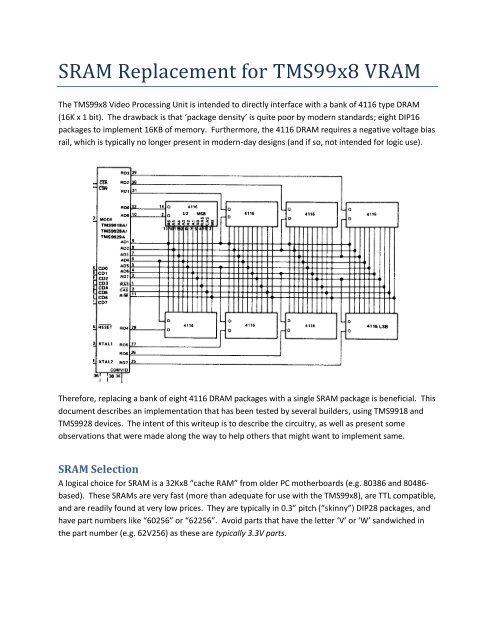
SRAM Replacement for TMS99x8 VRAMThe TMS99x8 Video Processing Unit is intended to directly interface with a bank of 4116 type DRAM(16K x 1 bit). The drawback is that ‘package density’ is quite poor by modern standards; eight DIP16packages to implement 16KB of memory. Furthermore, the 4116 DRAM requires a negative voltage biasrail, which is typically no longer present in modern-day designs (and if so, not intended for logic use).Therefore, replacing a bank of eight 4116 DRAM packages with a single SRAM package is beneficial. Thisdocument describes an implementation that has been tested by several builders, using TMS9918 andTMS9928 devices. The intent of this writeup is to describe the circuitry, as well as present someobservations that were made along the way to help others that might want to implement same.SRAM SelectionA logical choice for SRAM is a 32Kx8 “cache RAM” from older PC motherboards (e.g. 80386 and 80486-based). These SRAMs are very fast (more than adequate for use with the TMS99x8), are TTL compatible,and are readily found at very low prices. They are typically in 0.3” pitch (“skinny”) DIP28 packages, andhave part numbers like “60256” or “62256”. Avoid parts that have the letter ‘V’ or ‘W’ sandwiched inthe part number (e.g. 62V256) as these are typically 3.3V parts.
To properly implement address demultiplexing, care must be taken that the AD1-AD7 signals are stableprior to the rising edge of the ROW and COL signals (i.e. conform to the input setup time of the D FF).For a 74LS574, the setup time on the D0-D7 inputs prior to CLK rising edge is 20ns.First, consider the row address timing. The TMS9918 specification for t RA-RL is between 20 and 30ns, andso the additional t PD of an inverter (to make ROW from /RAS) ensures that in all cases the 20ns setuptime of the 74LS574 is met. For a 74HCT574, the setup time is 12ns, so once again there is no possibilityof a violation.Next, consider the column address timing. The TMS9918 specification for t CA-CL is no less than -10ns,with a typical of -2ns. The negative value means that /CAS is falling prior to the AD1-AD7 lines beingstable! If a 74LS04 inverter is used to create COL from /CAS, its t PLH of between 9ns and 15ns brings theworst-case setup time prior to COL rising to -1ns.A snapshot from a logic analyzer shows this issue clearly. The traces are (from top to bottom) COL,/CAS, and AD4-AD7. The cursor lines are positioned to illustrate that in this particular case, there areonly 14ns of setup time from AD7-AD0 becoming stable (in this case AD5 falling) and the rising edge ofCOL.This situation resulted in improper TMS9918 operation on my prototype; quite frequently the rowaddress would appear on the outputs of the column address latch. Clearly what was needed was moredelay between falling edge of /CAS and rising edge of COL. I accomplished this by creating COL from/CAS using three inverter stages in series, relying upon the propagation delay of the additional twoinverters to ensure the necessary setup time.
The analyzer snapshot below shows the improved timing, the traces (from top to bottom) are ROW,/RAS, COL, /CAS, and AD4-AD7.The time from AD7-AD0 settling and COL rising is now approximately 50ns; adequate to meet the setupof the 74LS574 D-FF. Because of this critical timing, it is advisable to use the same logic family for theinverters and the row and column address D-FF devices.SRAM Read Access Time RequirementsWhen reading from VRAM, the TMS9918 requires t SU(D-CH) of setup time during which the data on theRD7-RD0 inputs must be stable prior to the rising edge of /CAS. The specification for t SU(D-CH) is 60nsminimum. Refer to the analyzer snapshot we used for verification of the 3-inverter COL delay. We cansee that the column address is clocked about 210ns prior to the rising edge of /CAS. A cache SRAMtypically has 70ns access time or better, and the worst-case t PD of the 74LS574 is 28ns. Taking all timinginto account, the setup time of the RD7-RD0 inputs is met in all cases (210ns - 60ns - 70ns - 28ns = 52nsof margin) with LSTTL logic, even more so with HCT logic.VRAM Write Cycle AnalysisDuring a VRAM write cycle, the AD7-AD0 bus will contain the row address, the column address, andfinally the write data. The /RAS, /CAS, and R/W signals coordinate the transfer into DRAM. The VRAMwrite timing diagram from the TMS9918 VDP datasheet shows the signal behavior during the cycle.
It is not clear if the AD7-AD0 signals are not guaranteed to be stable throughout the entire write cycle:t w(W) is specified to be between 170ns and 210ns, and t WL-D between 135ns and 195ns. So, yet anotheroctal D-FF connected to AD7-AD0 is required, clocked after the write data is stable on AD7-AD0. Weneed to make a signal with a rising edge, call it WR, by inverting R/W.
This logic analyzer snapshot taking during a write cycle shows how all these signals work together; (fromtop to bottom) COL, /CAS, WR, R/W, and AD4-AD7.Here, the cursors are positioned on the rising edge of WR relative to AD4-AD7 becoming stable, showing23ns in between.The specification for t D-WL is between 0ns and 20ns, and a 74LS04 inverter will add between 9 and 15ns.The 20ns setup time requirement for the 74LS574 input is ‘cheated’ by 5ns with worst-case timing, soadding two additional inverter stages to provide more setup time would guarantee operation. I used a74HCT574 D-FF and one section of a 74HCT02 as an inverter, so the shorter HCT setup time was‘cheated’ by only 3ns. Using an LSTTL inverter and an HCT574 D-FF could be another possibleworkaround.Finally, recall that there was no need to pay any special attention to the relationship between AD7-AD1as applied to the row and column address flip-flops and A0-A14 of the 32Kx8 SRAM. This is not the case,however, with the relationship between AD7-AD0 and RD7-RD0. More specifically, there are no specialrequirements as to which SRAM D0-D7 terminal is connected to which RD[n] and which D-FF Q[n] line,but it is absolutely critical that there is a path between corresponding AD[n] and RD[n} terminals of theTMS99x8! The unorthodox weighting that TI used for the TMS9000 processor and peripherals makes iteasy to get lost and make an error in connections across the various busses. (Ask me how I know this…Ispent literally days trying to figure out why my test code resulted in only garbage on the screen!)
SRAM Replacement Schematic
SRAM Replacement for TMS91x8 Video DRAMThe TMS91x8 devices were released after the initial TMS99x8 family members. The only noticeabledifference between the TMS91x8 and its TMS99x8 counterpart is in the VRAM interface. The TMS91x8devices were redesigned to interface to a pair of TMS4416 (16Kx4) DRAM, rather than a bank of eight4116 DRAM. The TMS4416 does not suffer from the drawbacks of the 4116: two DIP18 packages versuseight DIP16 for a 16KB array, and no need for a negative bias rail. To accommodate the DIP18 package,the TMS4416 has four common data input and output terminals; there are no longer separate DI and DOterminals. This, in turn, means that the rather odd interface arrangement between the TMS9918 andthe 4116 DRAM cannot be used with the TMS4416 DRAM. What Texas Instruments did with theTMS91x8 was to simply make the RD7-RD0 bus a bidirectional data bus (rather than input only bus), andno longer place the write data on AD7-AD0 during a VRAM write cycle.The motivation to replace two TMS4416 DRAM with several D-FF and an SRAM is somewhat reduced,but the good news is that the TMS99x8 SRAM Replacement circuitry works with the TMS91x8 devicealso. The only modification required is that the Write Data D-FF is no longer required, and so if this FF isin a socket, it can simply be removed for compatibility with a TMS91x8. The row address timing remainsthe same, and the column address timing improves significantly. Therefore, the TMS99x8 and TMS91x8can be used interchangeably when this SRAM Replacement technique is used.
AcknowledgementsI would like to thank Andrew Lynch, creator of the wonderful N8VEM Z80 SBC project, for themotivation to work on the topic of SRAM replacement for the 4116 VRAM of the TMS9918. This hadbeen on my own “back burner” for many years until he gave me the ‘nudge’ I needed to get working onit. I would also like to thank Dan Werner, who started working on this topic around the same time, andarrived at a working prototype while I was still trying to get my own PCB working. Dan provided a gooddeal of moral support and things to think about when debugging. Dan and I eventually ended up withthe same circuit through our collaboration, which Andrew ultimately ended up building also.Tom LeMensetlemense@yahoo.comJanuary 24, 2010