HIGHPkSOLUTION
HIGHPkSOLUTION
HIGHPkSOLUTION

Create successful ePaper yourself
Turn your PDF publications into a flip-book with our unique Google optimized e-Paper software.
But when the hill (the oxide layer) is so narrow that you are<br />
counting individual atoms of thickness, the electron looks less<br />
like a ball and more like a wave. Specifically, it’s a wave that<br />
defines the probability of finding the electron in a particular<br />
location. The trouble is that the wave is actually broader than<br />
the hill, extending all the way to the other side and beyond. That<br />
means there is a distinct probability that an electron that should<br />
be on the gate side of the oxide can simply appear on the channel<br />
side, having “tunneled” through the energy barrier posed by the<br />
insulation rather than going over it.<br />
in The mid-1990s, we aT inTel and other major chip makers recognized<br />
that we were fast approaching the day when we would<br />
no longer be able to keep squeezing atoms out of the SiO 2 gate<br />
insulator. So we all launched research programs to come up with<br />
a better solution. The goal was to identify a gate dielectric material<br />
as a replacement for SiO 2 and also to demonstrate transistor<br />
prototypes that leaked less while at the same time driving<br />
plenty of current across the transistor channel. We needed a<br />
gate insulator that was thick enough to keep electrons from<br />
tunneling through it and yet permeable enough to let the gate’s<br />
electric field into the channel so that it could turn on the transistor.<br />
In other words, the material had to be physically thick<br />
but electrically thin.<br />
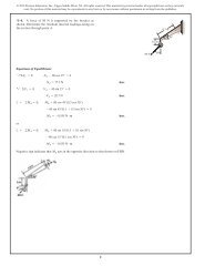
The technical term for such a material is a “high-k” dielectric;<br />
k, the dielectric constant, is a term that refers to a material’s<br />
ability to concentrate an electric field. Having a higher dielectric<br />
constant means the insulator can provide increased capacitance<br />
between two conducting plates—storing more charge—for<br />
the same thickness of insulator. Or if you prefer, it can provide<br />
the same capacitance with a thicker insulator [see illustration,<br />
“The High-k Way”]. SiO 2 typically has a k of around 4, while air<br />
and a vacuum have values of about 1. The k-value is related to<br />
how much a material can be polarized. When placed in an electric<br />
field, the charges in a dielectric’s atoms or molecules will reorient<br />
themselves in the direction of the field. These internal charges<br />
are more responsive in high-k dielectrics than in low-k ones.<br />
Incidentally, back in 2000, leading semiconductor firms began<br />
to change the material used to insulate the metal wires that connect<br />
transistors to each other from SiO 2 to low-k dielectrics. In<br />
the case of interconnects, you do not want the electric field from<br />
one wire to be felt in other nearby wires, because it creates a<br />
capacitor between the wires and can interfere with or slow down<br />
the signals on them. A low-k dielectric prevents the problem.<br />
We set about studying a veritable alphabet soup of high-k<br />
dielectric candidates, including aluminum oxide (Al 2O 3),<br />
SiO 2<br />
Jan. 2007 Working 45-nm<br />
HK+MG microprocessors<br />
demonstrated in systems<br />
2nd half 2007 High-volume<br />
production of 45-nm HK+MG<br />
microprocessors begins<br />
1990 2003<br />
2004<br />
2005<br />
2006<br />
2007<br />
Late 1990s SiO 2 ’s<br />
limits realized. Search<br />
begins for a high-k<br />
dielectric to replace it<br />
32 IEEE Spectrum | October 2007 | NA<br />
Metal<br />
High‑k<br />
Nov. 2003 Working<br />
high-k plus metal gate<br />
(HK+MG) research<br />
transistors<br />
titanium dioxide (TiO 2 ), tantalum pentoxide (Ta 2 O 5 ), hafnium<br />
dioxide (HfO 2 ), hafnium silicate (HfSiO 4 ), zirconium oxide (ZrO 2 ),<br />
zirconium silicate (ZrSiO 4 ), and lanthanum oxide (La 2 O 3 ). We<br />
were trying to identify such things as the material’s dielectric<br />
constant, how electrically stable it was, and its compatibility<br />
with silicon. For quick turnaround, we experimented with simple<br />
capacitor structures, building a sandwich consisting of titanium<br />
nitride electrodes, the high-k dielectric, and a silicon gate electrode.<br />
We then charged them up and discharged them again<br />
and again, watching to see how much the relationship between<br />
capacitance and voltage changed with each cycle.<br />
But for the first two years, all the dielectrics we tried worked<br />
poorly. We found that charges got trapped at the interface<br />
between the gate electrode and the dielectric. This accumulated<br />
charge within the capacitor altered the voltage level needed<br />
to store the same amount of energy in the capacitor from one<br />
charge-discharge cycle to the next. You want a transistor to<br />
operate exactly the same way every time it switches, but these<br />
gate-stack structures behaved differently each time they were<br />
charged up. The results were very discouraging, but eventually<br />
our team got an important break.<br />
It turned out that the problem lay in how we constructed<br />
the test capacitor. To make the dielectric layer, we were using<br />
one of two different semiconductor-manufacturing techniques:<br />
reactive sputtering and metal organic chemical vapor deposition.<br />
Unfortunately, both processes produce surfaces that,<br />
though remarkably smooth by most standards, were nevertheless<br />
uneven enough to leave some gaps and pockets in which<br />
charges could get stuck.<br />
We needed something even smoother—as smooth as a single<br />
layer of atoms, actually. So we turned to a technology called<br />
atomic layer deposition, so new that its debut in CMOS chip<br />
production comes only this year with our new high-k chips.<br />
Atomic layer deposition lets you build up a material one layer<br />
of atoms at a time. In this process, you introduce a gas that<br />
reacts with the surface of the silicon wafer, leaving the whole<br />
substrate coated in a single layer of atoms. Then, because there<br />
is no more surface to react with, the deposition stops. The gas is<br />
evacuated from the chamber and replaced with a second gas, one<br />
that chemically reacts with the layer of atoms just deposited. It<br />
too lays down one layer of atoms and then stops. You can repeat<br />
the process as many times as you want, to produce layered<br />
materials whose total thickness is controllable down to the<br />
width of a single atom.<br />
Deposited in this manner, both the hafnium- and zirconiumbased<br />
high-k dielectrics we studied showed much more stable<br />
Jan. 2006 Fully<br />
functional 1-billiontransistor<br />
45-nm<br />
HK+MG memory<br />
chips