HIGHPkSOLUTION
HIGHPkSOLUTION
HIGHPkSOLUTION

Create successful ePaper yourself
Turn your PDF publications into a flip-book with our unique Google optimized e-Paper software.
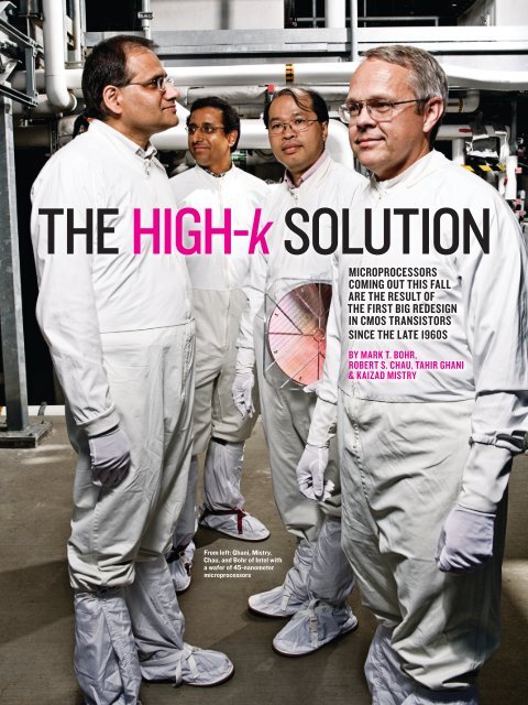
The high-k SoluTion<br />
Microprocessors<br />
coMing out this fall<br />
are the result of<br />
the first big redesign<br />
in cMos transistors<br />
since the late 1960s<br />
From left: Ghani, Mistry,<br />
Chau, and Bohr of Intel with<br />
a wafer of 45‑nanometer<br />
microprocessors<br />
bY MarK t. bohr,<br />
robert s. chau, tahir ghani<br />
& KaiZad MistrY
As you read this, two of our most advanced<br />
fabs here at Intel are gearing up for the<br />
commercial production of the latest<br />
Core 2 microprocessors, code-named<br />
Penryn, due to start rolling off the lines<br />
before the year is up. The chips, based on<br />
our latest 45-nanometer CMOS process technology<br />
will have more transistors and run faster and<br />
cooler than microprocessors fabricated with the<br />
previous, 65-nm process generation. For computeintensive<br />
music, video, and gaming applications,<br />
users will see a hefty performance increase over<br />
the best chips they are now using.<br />
A welcome development but hardly big news, right? After<br />
all, the density of transistors on chips has been periodically<br />
doubling, as predicted by Moore’s Law, for more than 40 years.<br />
The initial Penryn chips will be either dual-core processors with<br />
more than 400 million transistors or quad-core processors with<br />
more than 800 million transistors. You might think these chips<br />
don’t represent anything other than yet another checkpoint in<br />
the inexorable march of Moore’s Law.<br />
But you’d be wrong. The chips would not have been possible<br />
without a major breakthrough in the way we construct a key<br />
component of the infinitesimal transistors on those chips, called<br />
the gate stack. The basic problem we had to overcome was that<br />
a few years ago we ran out of atoms. Literally.<br />
To keep on the Moore’s Law curve, we need to halve the size<br />
of our transistors every 24 months or so. The physics dictates<br />
that the smallest parts of those transistors have to be diminished<br />
by a factor of 0.7. But there’s one critical part of the transistor<br />
that we found we couldn’t shrink anymore. It’s the thin<br />
layer of silicon dioxide (SiO 2 ) insulation that electrically isolates<br />
the transistor’s gate from the channel through which current<br />
flows when the transistor is on. That insulating layer has been<br />
IN THE FAB: By the end of 2007, two fabs at Intel will be churning out the first<br />
commercial microprocessors made up of transistors fundamentally redesigned<br />
using new materials.<br />
slimmed and shrunk with each new generation, about tenfold<br />
since the mid-1990s alone. Two generations before Penryn, that<br />
insulation had become a scant five atoms thick.<br />
We couldn’t shave off even one more tenth of a nanometer—<br />
a single silicon atom is 0.26 nm in diameter. More important, at<br />
a thickness of five atoms, the insulation was already a problem,<br />
wasting power by letting electrons rain through it. Without<br />
a significant innovation, the semiconductor industry was in<br />
danger of encountering the dreaded “showstopper,” the longawaited<br />
insurmountable problem that ends the Moore’s Law<br />
era of periodic exponential performance gains in memories,<br />
microprocessors, and other chips—and the very good times<br />
that have gone with it.<br />
The solution to this latest crisis involved thickening the<br />
insulator with more atoms, but of a different type, to give it better<br />
electrical properties. This new insulator works well enough<br />
to halt the power-sucking hail of electrons that’s plagued<br />
advanced chips for the past four years. If Moore’s Law crumbles<br />
in the foreseeable future, it won’t be because of inadequate gate<br />
insulation. Intel cofounder Gordon Moore, of Moore’s Law fame,<br />
called the alterations we made in introducing this latest generation<br />
of chips “the biggest change in transistor technology”<br />
since the late 1960s.<br />
As difficult as finding the new insulator was, that was only<br />
half the battle. The point of the insulator is to separate the<br />
transistor’s silicon gate from the rest of the device. The trouble<br />
is, a silicon gate didn’t work with the new insulator material. The<br />
initial transistors made with them performed worse than older<br />
transistors. The answer was to add yet another new material to<br />
the mix, swapping the silicon gate for one made of metal.<br />
It may not seem like such a big deal to change the materials<br />
used in a transistor, but it was. The industry went through<br />
a major upheaval several years ago when it switched from<br />
aluminum interconnects to copper ones and—at the same time—<br />
from SiO 2 cladding for those interconnects to chemically similar<br />
“low-k” dielectrics. And those changes had nothing to do with<br />
the transistor itself. A fundamental change to the composition<br />
of the transistor is pretty much unheard of. The combination of<br />
the gate and the insulator, the gate stack, hasn’t changed significantly<br />
since Moore, Andrew S. Grove, and others described<br />
it in this magazine back in October 1969!<br />
So when you boot up your next machine and you’re surprised by<br />
how fast it rips through some video coding, remember: there’s more<br />
new under its hood than in any computer you’ve ever owned.<br />
The story of how we and our co-workers solved the gateinsulation<br />
problem may seem esoteric, and in a literal way it is.<br />
But it is also emblematic of how Moore’s Law, the defining<br />
paradigm of the global semiconductor industry, is being sustained<br />
against often-daunting odds by the swift application of<br />
enormous intellectual and material resources to problems that,<br />
increasingly, are forcing engineers to struggle in realms until<br />
recently occupied only by physicists.<br />
The problem, ulTimaTely, is one of power. At five atoms, that sliver<br />
of SiO 2 insulation was so thin that it had begun to lose its insulating<br />
properties. Starting with the generation of chips fabricated<br />
in 2001, electrons had begun to trickle through it. In the<br />
processors made just two years later, that trickle became some<br />
100 times as intense.<br />
All that current was a drain on power and a source of<br />
unwanted heat. Laptops were heating up too much and draining<br />
their batteries too quickly. Servers were driving up their owners’<br />
electric bills and taxing their air conditioners. Even before we<br />
30 IEEE Spectrum | October 2007 | NA www.spectrum.ieee.org<br />
PrEvIOuS PAgE: AArON HEWITT; LEFT: INTEL;<br />
ILLuSTrATIONS: bryAN cHrISTIE dESIgN
n+<br />
Source<br />
+<br />
Gate<br />
Gate oxide<br />
+<br />
Channel<br />
+<br />
n+<br />
+ + +<br />
+ +<br />
+<br />
V+<br />
n+<br />
Drain<br />
ran out of atoms, designers had devised some tricks to throttle<br />
back on the power without losing speed. But without a way to<br />
stanch the unwanted flow of electrons through that sliver of<br />
insulation, the battle to make ever more powerful processors<br />
would soon be lost.<br />
To understand why, you need a quick lesson (or refresher)<br />
in semiconductor basics. The type of transistor that is chained<br />
together by the hundreds of millions to make up today’s microprocessors,<br />
memory, and other chips is called a metal-oxidesemiconductor<br />
field effect transistor, or MOSFET. Basically, it<br />
is a switch. A voltage on one terminal, known as the gate, turns<br />
on or off a flow of current between the two other terminals, the<br />
source and the drain [see illustration, “The Transistor”].<br />
MOSFETs come in two varieties: N (for n-type) MOS and<br />
P (for p-type) MOS. The difference is in the chemical makeup<br />
of the source, drain, and gate. Integrated circuits contain both<br />
NMOS and PMOS transistors. The transistors are formed on<br />
single-crystal silicon wafers; the source and drain are built by<br />
doping the silicon with impurities such as arsenic, phosphorus,<br />
or boron. Doping with boron adds positive charge carriers, called<br />
holes, to the silicon crystal, making it p-type, while doping with<br />
arsenic or phosphorus adds electrons, making it n-type.<br />
Taking an NMOS transistor as an example, the shallow<br />
source and drain regions are made of highly doped n-type silicon.<br />
Between them lies a lightly doped p-type region, called the<br />
transistor channel—where current flows. On top of the channel<br />
lies that thin layer of SiO 2 insulation, usually just called the<br />
gate oxide, which is the cause of the chip industry’s most recent<br />
technological headaches.<br />
Overlying that oxide layer is the gate electrode, which is<br />
made of partially ordered, or polycrystalline, silicon. In the case<br />
of an NMOS device it is also n-type. (The silicon gates replaced<br />
aluminum gates—the metal in “metal-oxide semiconductor”—<br />
in work described in the 1969 IEEE Spectrum article. But the<br />
“MOS” acronym has nevertheless lived on.)<br />
The NMOS transistor works like this: a positive voltage<br />
on the gate sets up an electric field across the oxide layer. The<br />
electric field repels the holes and attracts electrons to form an<br />
electron-conducting channel between the source and the drain.<br />
A PMOS transistor is just the complement of NMOS. The<br />
source and drain are p-type; the channel, n-type; and the gate,<br />
p-type. It works in the opposite manner as well: a positive voltage<br />
on the gate (as measured between the gate and source) cuts<br />
off the flow of current.<br />
In logic devices, PMOS and NMOS transistors are arranged so<br />
that their actions complement each other, hence the term CMOS<br />
for complementary metal-oxide semiconductor. The arrangement<br />
of CMOS circuits is such that they are designed to draw<br />
power only when the transistors are switching on or off. That’s<br />
the idea, anyway.<br />
n+<br />
V+<br />
n+<br />
+ + + + + + + +<br />
+<br />
+<br />
+<br />
+ +<br />
+ + - - - - - - - - -<br />
- - - - -<br />
- - +<br />
+<br />
THE TRANSISTOR: A positive voltage on the gate of an NMOS transistor drives<br />
positive charge in the channel away from the insulating gate oxide and attracts<br />
electrons, forming a path for electrons to flow.<br />
n+<br />
V+<br />
Channel<br />
Although the basic features and materials of the MOS transistor<br />
have stayed pretty much the same since the late 1960s, the<br />
dimensions have scaled dramatically. The transistor’s minimum<br />
layout dimensions were about 10 micrometers 40 years ago, and<br />
are less than 50 nm now, smaller by a factor of more than 200.<br />
Suppose a 1960s transistor was as big as a three-bedroom house<br />
and that it shrank by the same factor. You could hold the house<br />
in the palm of your hand today.<br />
In the Penryn processors that we recently began fabricating,<br />
most of their transistors’ features measure around 45 nm,<br />
though one is as small as 35 nm. It’s the first commercial microprocessor<br />
to have features this small; all other top-of-the-line<br />
microprocessors in production as this article is being written<br />
have 65-nm features. In other words, Penryn is the first<br />
of the 45-nm generation of microprocessors. Many more will<br />
soon follow.<br />
The thickness of the SiO 2 insulation on the transistor’s gate<br />
has scaled from about 100 nm down to 1.2 nm on state-of-theart<br />
microprocessors. The rate at which the thickness decreased<br />
was steady for years but started to slow at the 90-nm generation,<br />
which went into production in 2003. It was then that the oxide<br />
hit its five-atom limit. The insulator thickness shrank no further<br />
from the 90-nm to the 65-nm generation still common today.<br />
The reason the gate oxide was shrunk no further is that it<br />
began to leak current [see illustration, “Running Out of Atoms”].<br />
This leakage arises from quantum effects. At 1.2 nm, the quantum<br />
nature of particles starts to play a big role. We’re used to<br />
thinking of electrons in terms of classical physics, and we like<br />
to imagine an electron as a ball and the insulation as a tall and<br />
narrow hill. The height of the hill represents how much energy<br />
you’d need to provide the electron to get it to the other side. Give<br />
it a sufficient push and—sure enough—you could get it over the<br />
hill, busting through the insulation in the process.<br />
www.spectrum.ieee.org October 2007 | IEEE Spectrum | NA 31<br />
Energy<br />
Gate-oxide thickness (nm)<br />
10<br />
1<br />
-<br />
Thick<br />
gate oxide<br />
Gate<br />
SiO 2<br />
Energy<br />
Channel<br />
Technology generation (nm)<br />
High-k<br />
High-k<br />
350 180 90 45<br />
- -<br />
1.2-nm<br />
gate oxide<br />
Gate<br />
1000<br />
100<br />
10<br />
1<br />
0.1<br />
0.01<br />
RUNNING OUT OF ATOMS: The transistor’s gate oxide thinned with each new<br />
technology generation until it reached just 5 atoms (1.2 nm) thick. At that scale,<br />
the wave describing the probable location of an electron [red curve, top] is<br />
broader than the gate oxide, and the electron can simply appear on the other side<br />
of the gate oxide, having tunneled through the insulation. This so‑called gate<br />
leakage increased 100‑fold in the last three generations of transistors. A switch<br />
to a new gate oxide, a high‑k dielectric, was needed to plug the leak.<br />
Relative gate leakage
But when the hill (the oxide layer) is so narrow that you are<br />
counting individual atoms of thickness, the electron looks less<br />
like a ball and more like a wave. Specifically, it’s a wave that<br />
defines the probability of finding the electron in a particular<br />
location. The trouble is that the wave is actually broader than<br />
the hill, extending all the way to the other side and beyond. That<br />
means there is a distinct probability that an electron that should<br />
be on the gate side of the oxide can simply appear on the channel<br />
side, having “tunneled” through the energy barrier posed by the<br />
insulation rather than going over it.<br />
in The mid-1990s, we aT inTel and other major chip makers recognized<br />
that we were fast approaching the day when we would<br />
no longer be able to keep squeezing atoms out of the SiO 2 gate<br />
insulator. So we all launched research programs to come up with<br />
a better solution. The goal was to identify a gate dielectric material<br />
as a replacement for SiO 2 and also to demonstrate transistor<br />
prototypes that leaked less while at the same time driving<br />
plenty of current across the transistor channel. We needed a<br />
gate insulator that was thick enough to keep electrons from<br />
tunneling through it and yet permeable enough to let the gate’s<br />
electric field into the channel so that it could turn on the transistor.<br />
In other words, the material had to be physically thick<br />
but electrically thin.<br />
The technical term for such a material is a “high-k” dielectric;<br />
k, the dielectric constant, is a term that refers to a material’s<br />
ability to concentrate an electric field. Having a higher dielectric<br />
constant means the insulator can provide increased capacitance<br />
between two conducting plates—storing more charge—for<br />
the same thickness of insulator. Or if you prefer, it can provide<br />
the same capacitance with a thicker insulator [see illustration,<br />
“The High-k Way”]. SiO 2 typically has a k of around 4, while air<br />
and a vacuum have values of about 1. The k-value is related to<br />
how much a material can be polarized. When placed in an electric<br />
field, the charges in a dielectric’s atoms or molecules will reorient<br />
themselves in the direction of the field. These internal charges<br />
are more responsive in high-k dielectrics than in low-k ones.<br />
Incidentally, back in 2000, leading semiconductor firms began<br />
to change the material used to insulate the metal wires that connect<br />
transistors to each other from SiO 2 to low-k dielectrics. In<br />
the case of interconnects, you do not want the electric field from<br />
one wire to be felt in other nearby wires, because it creates a<br />
capacitor between the wires and can interfere with or slow down<br />
the signals on them. A low-k dielectric prevents the problem.<br />
We set about studying a veritable alphabet soup of high-k<br />
dielectric candidates, including aluminum oxide (Al 2O 3),<br />
SiO 2<br />
Jan. 2007 Working 45-nm<br />
HK+MG microprocessors<br />
demonstrated in systems<br />
2nd half 2007 High-volume<br />
production of 45-nm HK+MG<br />
microprocessors begins<br />
1990 2003<br />
2004<br />
2005<br />
2006<br />
2007<br />
Late 1990s SiO 2 ’s<br />
limits realized. Search<br />
begins for a high-k<br />
dielectric to replace it<br />
32 IEEE Spectrum | October 2007 | NA<br />
Metal<br />
High‑k<br />
Nov. 2003 Working<br />
high-k plus metal gate<br />
(HK+MG) research<br />
transistors<br />
titanium dioxide (TiO 2 ), tantalum pentoxide (Ta 2 O 5 ), hafnium<br />
dioxide (HfO 2 ), hafnium silicate (HfSiO 4 ), zirconium oxide (ZrO 2 ),<br />
zirconium silicate (ZrSiO 4 ), and lanthanum oxide (La 2 O 3 ). We<br />
were trying to identify such things as the material’s dielectric<br />
constant, how electrically stable it was, and its compatibility<br />
with silicon. For quick turnaround, we experimented with simple<br />
capacitor structures, building a sandwich consisting of titanium<br />
nitride electrodes, the high-k dielectric, and a silicon gate electrode.<br />
We then charged them up and discharged them again<br />
and again, watching to see how much the relationship between<br />
capacitance and voltage changed with each cycle.<br />
But for the first two years, all the dielectrics we tried worked<br />
poorly. We found that charges got trapped at the interface<br />
between the gate electrode and the dielectric. This accumulated<br />
charge within the capacitor altered the voltage level needed<br />
to store the same amount of energy in the capacitor from one<br />
charge-discharge cycle to the next. You want a transistor to<br />
operate exactly the same way every time it switches, but these<br />
gate-stack structures behaved differently each time they were<br />
charged up. The results were very discouraging, but eventually<br />
our team got an important break.<br />
It turned out that the problem lay in how we constructed<br />
the test capacitor. To make the dielectric layer, we were using<br />
one of two different semiconductor-manufacturing techniques:<br />
reactive sputtering and metal organic chemical vapor deposition.<br />
Unfortunately, both processes produce surfaces that,<br />
though remarkably smooth by most standards, were nevertheless<br />
uneven enough to leave some gaps and pockets in which<br />
charges could get stuck.<br />
We needed something even smoother—as smooth as a single<br />
layer of atoms, actually. So we turned to a technology called<br />
atomic layer deposition, so new that its debut in CMOS chip<br />
production comes only this year with our new high-k chips.<br />
Atomic layer deposition lets you build up a material one layer<br />
of atoms at a time. In this process, you introduce a gas that<br />
reacts with the surface of the silicon wafer, leaving the whole<br />
substrate coated in a single layer of atoms. Then, because there<br />
is no more surface to react with, the deposition stops. The gas is<br />
evacuated from the chamber and replaced with a second gas, one<br />
that chemically reacts with the layer of atoms just deposited. It<br />
too lays down one layer of atoms and then stops. You can repeat<br />
the process as many times as you want, to produce layered<br />
materials whose total thickness is controllable down to the<br />
width of a single atom.<br />
Deposited in this manner, both the hafnium- and zirconiumbased<br />
high-k dielectrics we studied showed much more stable<br />
Jan. 2006 Fully<br />
functional 1-billiontransistor<br />
45-nm<br />
HK+MG memory<br />
chips
INTEL (4)<br />
electrical characteristics in comparison<br />
with the ones formed by<br />
sputtering or chemical vapors. The<br />
trapped-charge problem seemed to<br />
have been smoothed out.<br />
wiTh Two candidaTe maTerials idenTified,<br />
we started making NMOS and<br />
PMOS transistors out of them. Then<br />
came the next snag. These transistors,<br />
pretty much identical to our<br />
existing transistors except for the<br />
different dielectric, had a few problems.<br />
For one thing, it took more<br />
voltage to turn them on than it<br />
should have—what’s called Fermilevel<br />
pinning. For another, once the<br />
+ + +<br />
k = 1<br />
- - -<br />
transistors were on, the charges moved sluggishly through<br />
them—slowing the device’s switching speed. This problem<br />
is known as low charge-carrier mobility.<br />
We weren’t the only ones encountering these problems; just<br />
about everybody else was struggling with them, too. With the<br />
countdown in progress for the next generation predicted by<br />
Moore’s Law, understanding why the high-k dielectric transistors<br />
performed so poorly and finding a solution became an<br />
urgent task. Using a combination of experimental work and<br />
physics-based models, we began to figure out what had gone<br />
wrong. The source of the trouble, ultimately, came down to<br />
the interaction between the polysilicon gate electrode and the<br />
new high-k dielectrics.<br />
Why this is so has a complicated explanation. The dielectric<br />
layer is made up of dipoles—objects with a positive pole and a negative<br />
one. This is the very aspect that gives the high-k dielectric<br />
such a high dielectric constant. These dipoles vibrate like a taut<br />
rubber band and lead to strong vibrations in a semiconductor’s<br />
crystal lattice, called phonons [see illustration, “Bumpy Ride”].<br />
These phonons knock around passing electrons, slowing them<br />
down and reducing the speed at which the transistor can switch.<br />
But theoretical studies and computer simulations performed by<br />
us and others showed a way out. The simulations indicated that<br />
the influence of dipole vibrations on the channel electrons can be<br />
screened out by significantly increasing the density of electrons<br />
in the gate electrode. One way to do that would be to switch from<br />
a polysilicon gate to a metal one. As a conductor, metal can pack<br />
in hundreds of times more electrons than silicon. Experiments<br />
and further computer simulations confirmed that metal gates<br />
would do the trick, screening out the phonons and letting current<br />
flow smoothly through the transistor channel.<br />
What’s more, the bond between the high-k dielectric and<br />
the metal gate would be so much better than that between the<br />
dielectric and the silicon gate that our other problem, Fermilevel<br />
pinning, would be solved by a metal gate as well.<br />
now our engineers had a ne w major chore: find a metal they<br />
could use for the gate electrode that would combine well with<br />
the new high-k dielectric. Because the electrical characteristics<br />
of the gates of NMOS and PMOS transistors are different, they<br />
actually needed not one metal but two—one for NMOS and one<br />
for PMOS.<br />
Just as standard MOS transistors use n-type and p-type<br />
polysilicon gates for NMOS and PMOS transistors, high-k transistors<br />
would need metal gate electrode materials with a key<br />
property similar to polysilicon’s. This key property is known<br />
V+<br />
+ + + + + +<br />
k = 2<br />
- - - - - -<br />
+ + +<br />
k = 2<br />
- - -<br />
THE HIGH‑K WAY: The dielectric constant, k, is a measure of an insulator’s ability to concentrate an electric field.<br />
If one gate oxide has twice the dielectric constant of another, a given voltage will draw twice as much charge into the<br />
transistor channel. Or, the same amount of charge will accumulate, if the higher‑k dielectric is made twice as thick.<br />
as the work function. In this context, work function refers to<br />
the energy of an electron in the gate electrode relative to that<br />
of an electron in the lightly doped silicon channel. The energy<br />
difference sets up an electric field that can modulate to the<br />
amount of voltage needed to begin to turn the transistor on,<br />
the threshold voltage. Unless the gate’s work function is chosen<br />
well, the threshold voltage will be too high, and the transistor<br />
will not turn on easily enough.<br />
We analyzed, modeled, and experimented with many types<br />
of metals, some with work functions that more closely matched<br />
highly doped silicon than others. But by themselves, none had<br />
exactly the work function of the doped silicon, so we had to<br />
learn to change the work function of metals to suit our needs.<br />
Eventually, the research group identified NMOS and PMOS metals<br />
by first building capacitors out of them and then transistors.<br />
We cannot disclose the exact makeup of our metal layers,<br />
because after all, the IC industry is very competitive!<br />
We built our first NMOS and PMOS high-k and metal gate<br />
transistors in mid-2003 in Intel’s Hillsboro, Ore., development<br />
fab. We started out using Intel’s 130-nm technology, which was<br />
about three years old at the time and was used in high-volume<br />
production. The transistors, with a hafnium-based oxide and<br />
metal gate electrodes, had everything we needed: they turned<br />
on at the right voltage, leaked little current through the gate<br />
oxide, and passed a large amount of current through the channel<br />
for a given voltage. And that current moved quickly. In fact,<br />
for a given off-state current, these first transistors drove more<br />
current than any transistor reported at the time.<br />
of course, we weren’T alone. And there were still plenty of unknowns.<br />
By 2003, researchers in university labs and other semiconductor<br />
firms around the world had zeroed in on hafnium-based materials<br />
as the gate dielectric. A variety of them were under earnest<br />
study: hafnium oxides, hafnium silicates, and hafnium oxides<br />
containing nitrogen. The method of forming the high-k film, too,<br />
was unsettled, with different groups trying sputtering, chemical<br />
vapor deposition, and atomic layer deposition, which we eventually<br />
settled on. But the biggest unknowns at the time were<br />
what metal gate materials to use and how to fit them into the<br />
transistor-manufacturing process.<br />
The normal fabrication method is known as “gate first.” As<br />
the name implies, the gate dielectric and gate electrodes are<br />
constructed first. Then the dopants for the source and drain are<br />
implanted into the silicon on either side of the gate. Finally, the<br />
silicon is annealed to repair the damage from the implantation<br />
process. That procedure requires that the gate electrode material<br />
www.spectrum.ieee.org October 2007 | IEEE Spectrum | NA 33
e able to withstand the high temperatures used in the annealing<br />
step—not a problem for polycrystalline silicon but potentially a<br />
big one for some metals.<br />
To make a long story short, the search for gate electrode<br />
materials with both the right work function and tolerance to<br />
high-temperature processing was very difficult and full of dead<br />
ends. Especially for the PMOS transistor.<br />
Another transistor process sequence, dubbed “gate last,”<br />
circumvents the thermal annealing requirement by depositing<br />
the gate electrode materials after the source and drain are<br />
formed. However, many of our peers saw the gate-last process,<br />
which we ultimately adopted, as too much of a departure and<br />
too challenging.<br />
Meanwhile, a third approach remarkable in its simplicity<br />
emerged. Called fully silicided gates, it lets you follow the<br />
normal gate-first process but then lets you turn the polysilicon<br />
gate into a metal-silicide<br />
gate, essentially replacing every<br />
other silicon atom with metal (usually<br />
nickel). Then, by doping the Polysilicon gate<br />
nickel silicide, you can alter its work<br />
-<br />
function for use in either an NMOS<br />
device or a PMOS one. By late 2006, High-k Polysilicon dielectric gate<br />
though, nearly everyone, includ-<br />
-<br />
ing us, had given up on the fully<br />
silicided gates approach. No one High-k dielectric<br />
could move the silicide’s work function<br />
quite close enough to where it<br />
needed to be.<br />
Nevertheless, the search goes on<br />
at other major chip makers to find<br />
the materials with the right work<br />
function that could survive high Metal gate<br />
temperatures and enable the industry<br />
standard gate-first process flow.<br />
Metal gate<br />
having builT well-funcTioning TransisTors<br />
using old technology, in the second<br />
half of 2003 it was time to move<br />
from research to development of<br />
high-k dielectric plus metal gate<br />
transistors, as we called them.<br />
Engineers began working to determine<br />
whether these early transistors<br />
could be scaled to the upcoming<br />
High-k dielectric<br />
45-nm dimensions and still meet the rigorous performance,<br />
reliability, and manufacturability requirements of an advanced<br />
microprocessor technology.<br />
It was no cakewalk. The research group engineers had provided<br />
a critical lead in identifying promising high-k and metal<br />
gate materials, but the NMOS and PMOS transistors had not<br />
yet been combined on one wafer as they would be in a microprocessor,<br />
using a manufacturing process that could make both.<br />
What’s more, there were hard questions still to be answered<br />
about how many good chips we could expect for every bad one<br />
(yield) and how reliable those chips would be.<br />
During the months that followed, the team cracked one<br />
problem after another—making changes to materials, chemical<br />
recipes, and manufacturing processes. It wasn’t until late 2004<br />
that the team felt it had enough convincing data that the new<br />
transistors could be made to work on our 45-nm technology.<br />
At that point, there was no turning back. Intel was now committed<br />
to making a high-k dielectric plus metal gate transistor<br />
structure using the gate-last process flow. It was a gutsy call.<br />
Our team knew it was committing all of Intel’s next generation<br />
of microprocessors to the biggest change in transistor technology<br />
in 40 years.<br />
The next key milestone was to demonstrate working test<br />
chips using the final scaled dimensions combined with the new<br />
transistor features. The traditional chip to test a new technology<br />
on is static random access memory, or SRAM, which is the type<br />
of memory collocated on the same chip with the microprocessor.<br />
Typically, microprocessor makers have designs for SRAM that<br />
are a year or more ahead of their processor designs. SRAM is a<br />
very regular array of memory cells, each of which consists of six<br />
densely packed and interconnected transistors. Because of their<br />
density and regularity, SRAM chips provide good data on how<br />
many defects a manufacturing process produces.<br />
Our first fully functional test SRAM chips with the new transistors<br />
came off the line in January<br />
2006. They were of a 153-megabit<br />
- -<br />
-<br />
-<br />
- -<br />
-<br />
-<br />
- -<br />
-<br />
-<br />
-<br />
- - - -<br />
-<br />
- -<br />
-<br />
-<br />
-<br />
- -<br />
- - - -<br />
Channel<br />
BUMPY RIDE: The particular density of electrons in a traditional<br />
polysilicon gate allowed inherent vibrations in the high‑k dielectric<br />
to move into the transistor channel and Channel disrupt the flow of current.<br />
High-k dielectric<br />
Channel<br />
-<br />
- - - - - - -<br />
- - - - - - -<br />
- - - - - - -<br />
------ ------ --<br />
- - - - - - -<br />
- - - - - - -<br />
- - - - - - -<br />
Channel<br />
The higher density of electrons in a metal screened out the<br />
vibrations, allowing current to flow more smoothly.<br />
-<br />
design consisting of more than<br />
1 billion transistors. Each sixtransistor<br />
memory cell in the chip<br />
occupied little more than one-third<br />
of a square micrometer. This test chip<br />
had all the features needed to build<br />
a 45-nm microprocessor, including<br />
the high-k plus metal gate transistors<br />
and nine layers of copper interconnects.<br />
Considering how new and<br />
radically different the transistor and<br />
manufacturing process were, it was<br />
a surprise even to some of the engineers<br />
in the development group that<br />
it all worked together so well. Even so,<br />
the development team still had a lot<br />
ahead of it to bring the performance,<br />
reliability, and yield of the process up<br />
to the level needed for manufacturing<br />
microprocessors.<br />
The new gate stack worked wonders<br />
in battling leakage through the<br />
gate, reducing it by more than a factor<br />
of 10. But the gate oxide is not<br />
the only source of transistor leakage<br />
chip makers have to worry about.<br />
The other significant leak is called<br />
source-to-drain or subthreshold leakage. It’s a trickle of current<br />
seen even when the transistor is intended to be in the “off” state.<br />
Making transistors smaller has also meant steadily lowering the<br />
amount of voltage needed to turn them on, the threshold voltage.<br />
Unfortunately, steadily lowering the threshold voltage lets<br />
more current slip through. For many years, each new generation<br />
of transistor would increase drive current (and improve performance)<br />
by about 30 percent but would pay the price of about<br />
a threefold increase in subthreshold leakage. Leakage currents<br />
have reached levels high enough to be a noticeable portion of<br />
total microprocessor power consumption.<br />
The industry is now in an era where power efficiency and<br />
low leakage are more important than raw speed increases. But<br />
a transistor can be designed to operate to favor either priority<br />
by adjusting the channel length or adjusting the threshold<br />
voltage. A shorter channel leaks more but allows for a higher<br />
drive current. A higher threshold voltage pinches off the leak<br />
but also throttles the drive current. Adjusting the threshold<br />
34 IEEE Spectrum | October 2007 | NA www.spectrum.ieee.org
CONVENTIONAL TRANSISTORS<br />
Gate<br />
Gate oxide<br />
Source<br />
Proprietary<br />
metal<br />
composition<br />
Thicker<br />
gate oxide<br />
Polycrystalline<br />
silicon<br />
Silicon dioxide<br />
Silicon<br />
Channel<br />
HIGH-k TRANSISTORS<br />
Polycrystalline<br />
silicon<br />
High-k dielectric<br />
Silicon<br />
High-k dielectric<br />
Silicon<br />
Drain<br />
Smoother layer<br />
via ALD deposition<br />
method<br />
Metal<br />
Energy<br />
Energy<br />
PROBLEM: Electron leakage through gate oxide<br />
Channel<br />
Channel<br />
- -<br />
1.2-nm<br />
gate oxide<br />
V+<br />
- - -<br />
- - - -<br />
-<br />
Thick<br />
gate oxide<br />
Gate<br />
PROBLEM: Uneven dielectric<br />
surface traps charges.<br />
HIGH-k PLUS METAL GATE SOLUTION: Thicker, high-k<br />
gate oxide prevents electron<br />
leakage.<br />
voltage is where the high-k dielectric comes into play. A thicker<br />
dielectric reduces the gate’s ability to open a conductive channel<br />
between the source and the drain, increasing the threshold<br />
voltage. A thinner dielectric layer has the opposite effect.<br />
Compared with the previous 65-nm transistors, 45-nm high-k<br />
plus metal gate transistors provide either a 25 percent increase<br />
in drive current at the same subthreshold leakage or more than<br />
a fivefold reduction in leakage at the same drive current, or<br />
anywhere between those values. We can make the choice on<br />
a product-by-product basis, or different circuits on the same<br />
microprocessor chip can use different transistors to optimize<br />
for performance or power.<br />
in january 2007, Intel made the first working 45-nm microprocessors<br />
using these revolutionary high-k plus metal gate<br />
transistors. One was the Penryn dual-core microprocessor,<br />
which has 410 million transistors. Different versions of Penryn<br />
will be optimized for mobile, desktop, workstation, and server<br />
applications. The quad-core version of this product will have<br />
820 million transistors. Penryn was followed a few months later<br />
by Silverthorne, a single-core microprocessor with 47 million<br />
transistors that is designed for low-power applications, including<br />
mobile Internet devices and ultramobile PCs. There are more<br />
than 15 new chips under development at Intel using our new<br />
technology. Production of Penryn and Silverthorne will start<br />
later this year at Intel plants in Oregon and Arizona. Next year,<br />
we’ll start up the process at two other high-volume manufacturing<br />
fabs, in New Mexico and Israel.<br />
The invention of high-k plus metal gate transistors was an<br />
important breakthrough. Although we could have continued to<br />
shrink transistors to fit the dimensions needed for the 45-nm<br />
Gate<br />
PROBLEM: Phonons<br />
scatter electrons in channel.<br />
- - - - - - - -<br />
V+<br />
-<br />
- - -<br />
- - - -<br />
-<br />
- -<br />
-<br />
SOLUTION: New atomiclayer<br />
deposition creates<br />
smooth dielectric layer.<br />
PROBLEM SOLVED: Transistors of the 65‑nm<br />
generation were plagued by electrons that<br />
tunneled through the gate insulation.<br />
Switching to a high‑k dielectric as a gate oxide<br />
solved that problem but introduced others.<br />
Those problems were solved by the introduc‑<br />
tion of a new deposition technique and<br />
swapping the silicon gate material for two<br />
types of metal gates, allowing for the<br />
introduction of 45‑nm microprocessors.<br />
PROBLEM: Poor bonding<br />
between gate and dielectric<br />
makes transistor hard to turn on.<br />
V+<br />
SOLUTION: Metal gate’s higher<br />
electron density screens out<br />
electron-scattering phonons.<br />
- - - - - - -<br />
- - - - - -<br />
- - - - - - -<br />
-<br />
Metal and<br />
high-k dielectric<br />
bond well<br />
generation without this breakthrough, those transistors would<br />
not have worked much better than their predecessors, and they<br />
certainly would have expended more watts. We’re confident this<br />
new transistor can be scaled further, and development is already<br />
well under way on our next-generation 32-nm transistors using an<br />
improved version of high-k plus metal gate technology. Whether<br />
this type of transistor structure will continue to scale to the next<br />
two generations—22 nm and 16 nm—is a question for the future.<br />
Will we need new materials and new structures again?<br />
Nobody knows for sure. But that is what makes integrated<br />
circuit research and development so exciting. n<br />
AbOuT THE AuTHOrS<br />
MArK T. bOHr, an IEEE Fellow, is the director of process<br />
architecture and integration at Intel. rObErT S. cHAu,<br />
an IEEE Fellow, is the director of transistor research<br />
and nanotechnology. TAHIr gHANI, an IEEE member, is<br />
the director of transistor technology and integration.<br />
KAIZAd MISTry, an IEEE senior member, manages the<br />
development of Intel’s 45‑nanometer cMOS technology in<br />
the logic and technology development group.<br />
TO PrObE FurTHEr<br />
robert S. chau and colleagues explained the problem that<br />
led to the use of a metal gate in detail in “High‑k/Metal‑gate<br />
Stack and Its MOSFET characteristics,” IEEE Electron Device<br />
Letters, June 2004.<br />
Intel and others will be presenting the latest high‑k<br />
dielectric and metal gate transistor research at IEEE’s 2007<br />
International Electron devices Meeting, in Washington, d.c.,<br />
from 10 to 12 december.<br />
www.spectrum.ieee.org October 2007 | IEEE Spectrum | NA 35