DM74LS191 Synchronous 4-Bit Up/Down Counter with Mode Control
DM74LS191 Synchronous 4-Bit Up/Down Counter with Mode Control
DM74LS191 Synchronous 4-Bit Up/Down Counter with Mode Control
- No tags were found...

Create successful ePaper yourself
Turn your PDF publications into a flip-book with our unique Google optimized e-Paper software.
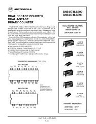
August 1986Revised February 1999<strong>DM74LS191</strong><strong>Synchronous</strong> 4-<strong>Bit</strong> <strong>Up</strong>/<strong>Down</strong> <strong>Counter</strong> <strong>with</strong> <strong>Mode</strong> <strong>Control</strong>General DescriptionThe <strong>DM74LS191</strong> circuit is a synchronous, reversible, up/down counter. <strong>Synchronous</strong> operation is provided by havingall flip-flops clocked simultaneously, so that the outputschange simultaneously when so instructed by the steeringlogic. This mode of operation eliminates the output countingspikes normally associated <strong>with</strong> asynchronous (rippleclock) counters.The outputs of the four master-slave flip-flops are triggeredon a LOW-to-HIGH level transition of the clock input, if theenable input is LOW. A HIGH at the enable input inhibitscounting. Level changes at either the enable input or thedown/up input should be made only when the clock input isHIGH. The direction of the count is determined by the levelof the down/up input. When LOW, the counter counts upand when HIGH, it counts down.The counter is fully programmable; that is, the outputs maybe preset to either level by placing a LOW on the load inputand entering the desired data at the data inputs. The outputwill change independent of the level of the clock input. Thisfeature allows the counters to be used as modulo-N dividersby simply modifying the count length <strong>with</strong> the presetinputs.The clock, down/up, and load inputs are buffered to lowerthe drive requirement; which significantly reduces the numberof clock drivers, etc., required for long parallel words.Ordering Code:Two outputs have been made available to perform the cascadingfunction: ripple clock and maximum/minimum count.The latter output produces a high-level output pulse <strong>with</strong> aduration approximately equal to one complete cycle of theclock when the counter overflows or underflows. The rippleclock output produces a low-level output pulse equal inwidth to the low-level portion of the clock input when anoverflow or underflow condition exists. The counters can beeasily cascaded by feeding the ripple clock output to theenable input of the succeeding counter if parallel clockingis used, or to the clock input if parallel enabling is used.The maximum/minimum count output can be used toaccomplish look-ahead for high-speed operation.Features■ Counts binary■ Single down/up count control line■ Count enable control input■ Ripple clock output for cascading■ Asynchronously presettable <strong>with</strong> load control■ Parallel outputs■ Cascadable for n-bit applications■ Average propagation delay 20 ns■ Typical clock frequency 25 MHz■ Typical power dissipation 100 mW<strong>DM74LS191</strong> <strong>Synchronous</strong> 4-<strong>Bit</strong> <strong>Up</strong>/<strong>Down</strong> <strong>Counter</strong> <strong>with</strong> <strong>Mode</strong> <strong>Control</strong>Order Number Package Number Package Description<strong>DM74LS191</strong>M M16A 16-Lead Small Outline Integrated Circuit (SOIC), JEDEC MS-012, 0.150” Narrow Body<strong>DM74LS191</strong>N N16E 16-Lead Plastic Dual-In-Line Package (PDIP), JEDEC MS-001, 0.300” WideDevices also available in Tape and Reel. Specify by appending the suffix letter “X” to the ordering code.© 1999 Fairchild Semiconductor Corporation DS006405.prf www.fairchildsemi.com
<strong>DM74LS191</strong>Connection DiagramTiming Diagramwww.fairchildsemi.com 2
Logic Diagram<strong>DM74LS191</strong>Pin (16) = V CC , Pin (8) = GND3 www.fairchildsemi.com
<strong>DM74LS191</strong>Absolute Maximum Ratings(Note 1)Storage Temperature Range−65°C to +150°CInput Voltage7VOperating Free Air Temp. Range0°C to +70°CSupply Voltage7VNote 1: The “Absolute Maximum Ratings” are those values beyond whichthe safety of the device cannot be guaranteed. The device should not beoperated at these limits. The parametric values defined in the ElectricalCharacteristics tables are not guaranteed at the absolute maximum ratings.The “Recommended Operating Conditions” table will define the conditionsfor actual device operation.Recommended Operating ConditionsSymbol Parameter Min Nom Max UnitsV CC Supply Voltage 4.75 5 5.25 VV IH HIGH Level Input Voltage 2 VV IL LOW Level Input Voltage 0.8 VI OH HIGH Level Output Current −0.4 mAI OL LOW Level Output Current 8 mAf CLK Clock Frequency (Note 2) 0 20 MHzt W Pulse Width Clock 25 ns(Note 2) Load 35t SU Data Setup Time (Note 2) 20 nst H Data Hold Time (Note 2) 0 nst EN Enable Time to Clock (Note 2) 30 nsT A Free Air Operating Temperature 0 70 °CNote 2: T A = 25°C and V CC = 5V.DC Electrical CharacteristicsSymbol Parameter Conditions Min Typ Max Units(Note 3)V I Input Clamp Voltage V CC = Min, I I = − 18 mA −1.5 VV OH HIGH Level Output V CC = Min, I OH = Max Mil 2.5 3.4Voltage V IL = Max, V IH = Min Com 2.7 3.4 VV OL LOW Level Output V CC = Min, I OL = Max 0.25 0.4Voltage V IL = Max, V IH = Min 0.35 0.5 VI OL = 4 mA, V CC = Min 0.25 0.4I I Input Current @ Max V CC = Max Enable 0.3 mAInput Voltage V I = 7V Others 0.1I IH HIGH Level Input V CC = Max Enable 60 µACurrent V I = 2.7V Others 20I IL LOW Level Input V CC = Max Enable −1.08 mACurrent V I = 0.4V Others −0.4I OS Short Circuit V CC = Max Mil −20 −100 mAOutput Current (Note 4) Com −20 −100I CC Supply Current V CC = Max (Note 5) 20 35 mANote 3: All typicals are at V CC = 5V, T A = 25°C.Note 4: Not more than one output should be shorted at a time, and the duration should not exceed one second.Note 5: I CC is measured <strong>with</strong> all inputs grounded and all outputs open.www.fairchildsemi.com 4
AC Electrical CharacteristicsFrom (Input)R L = 2 kΩSymbol Parameter To (Output) C L = 15 pF C L = 50 pF UnitsMin Max Min Maxf MAX Maximum Clock 20 20 MHzFrequencyt PLH Propagation Delay Time Load to 33 43 nsLOW-to-HIGH Level OutputAny Qt PHL Propagation Delay Time Load to 50 59 nsHIGH-to-LOW Level OutputAny Qt PLH Propagation Delay Time Data to 22 26 nsLOW-to-HIGH Level OutputAny Qt PHL Propagation Delay Time Data to 50 62 nsHIGH-to-LOW Level OutputAny Qt PLH Propagation Delay Time Clock to 20 24 nsLOW-to-HIGH Level OutputRipple Clockt PHL Propagation Delay Time Clock to 24 33 nsHIGH-to-LOW Level OutputRipple Clockt PLH Propagation Delay Time Clock to 24 29 nsLOW-to-HIGH Level OutputAny Qt PHL Propagation Delay Time Clock to 36 45 nsHIGH-to-LOW Level OutputAny Qt PLH Propagation Delay Time Clock to 42 47 nsLOW-to-HIGH Level OutputMax/Mint PHL Propagation Delay Time Clock to 52 65 nsHIGH-to-LOW Level OutputMax/Mint PLH Propagation Delay Time <strong>Up</strong>/<strong>Down</strong> to 45 50 nsLOW-to-HIGH Level OutputRipple Clockt PHL Propagation Delay Time <strong>Up</strong>/<strong>Down</strong> to 45 54 nsHIGH-to-LOW Level OutputRipple Clockt PLH Propagation Delay Time <strong>Down</strong>/<strong>Up</strong> to 33 36 nsLOW-to-HIGH Level OutputMax/Mint PHL Propagation Delay Time <strong>Down</strong>/<strong>Up</strong> to 33 42 nsHIGH-to-LOW Level OutputMax/Mint PLH Propagation Delay Time Enable to 33 36 nsLOW-to-HIGH Level OutputRipple Clockt PHL Propagation Delay Time Enable to 33 42 nsHIGH-to-LOW Level OutputRipple Clock<strong>DM74LS191</strong>5 www.fairchildsemi.com
<strong>DM74LS191</strong> <strong>Synchronous</strong> 4-<strong>Bit</strong> <strong>Up</strong>/<strong>Down</strong> <strong>Counter</strong> <strong>with</strong> <strong>Mode</strong> <strong>Control</strong>Physical Dimensions inches (millimeters) unless otherwise noted16-Lead Small Outline Integrated Circuit (SOIC), JEDEC MS012, 0.150” Narrow BodyPackage Number M16A16-Lead Plastic Dual-In-Line Package (PDIP), JEDEC MS-001, 300” WidePackage Number N16ELIFE SUPPORT POLICYFAIRCHILD’S PRODUCTS ARE NOT AUTHORIZED FOR USE AS CRITICAL COMPONENTS IN LIFE SUPPORTDEVICES OR SYSTEMS WITHOUT THE EXPRESS WRITTEN APPROVAL OF THE PRESIDENT OF FAIRCHILDSEMICONDUCTOR CORPORATION. As used herein:1. Life support devices or systems are devices or systemswhich, (a) are intended for surgical implant into thebody, or (b) support or sustain life, and (c) whose failureto perform when properly used in accordance <strong>with</strong>instructions for use provided in the labeling, can be reasonablyexpected to result in a significant injury to theuser.2. A critical component in any component of a life supportdevice or system whose failure to perform can be reasonablyexpected to cause the failure of the life supportdevice or system, or to affect its safety or effectiveness.www.fairchildsemi.comFairchild does not assume any responsibility for use of any circuitry described, no circuit patent licenses are implied and Fairchild reserves the right at any time <strong>with</strong>out notice to change said circuitry and specifications.