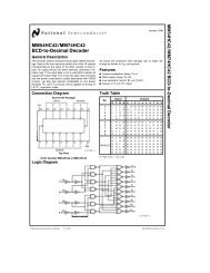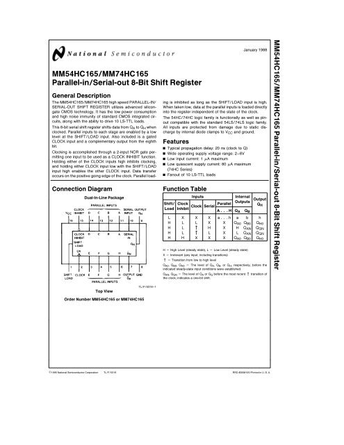
MM54HC165/MM74HC165 Parallel-in/Serial-out 8-Bit Shift Register
MM54HC165/MM74HC165 Parallel-in/Serial-out 8-Bit Shift Register
MM54HC165/MM74HC165 Parallel-in/Serial-out 8-Bit Shift Register

You also want an ePaper? Increase the reach of your titles
YUMPU automatically turns print PDFs into web optimized ePapers that Google loves.
AC Electrical Characteristics V CC e5V T A e25C C L e15 pF t r et f e6nsSymbol Parameter Conditions Typ Guaranteed Limit Unitsf MAX Maximum Operat<strong>in</strong>g Frequency 50 30 MHzt PHL t PLH Maximum Propagation Delay H to Q H or Q H 15 25 nst PHL t PLH Maximum Propagation Delay 13 25 ns<strong>Serial</strong> <strong>Shift</strong><strong>Parallel</strong> Load to Q Ht PHL t PLH Maximum Propagation Delay 15 25 nsClock to Outputt S M<strong>in</strong>imum Setup Time <strong>Serial</strong> Input 10 20 nsto Clock <strong>Parallel</strong> or Data to <strong>Shift</strong>Loadt S M<strong>in</strong>imum Setup Time <strong>Shift</strong>Load to Clock 11 20 nst S M<strong>in</strong>imum Setup Time Clock Inhibit to Clock 10 20 nst H M<strong>in</strong>imum Hold Time <strong>Serial</strong> 0 nsInput to Clock or<strong>Parallel</strong> Data to <strong>Shift</strong>Loadt W M<strong>in</strong>imum Pulse Width Clock 16 nsAC Electrical Characteristics C L e50 pF t r et f e6 ns (unless otherwise specified)74HC54HCT A e25CSymbol Parameter Conditions V CC T A eb40 to 85C T A eb55 to 125C UnitsTypGuaranteed Limitsf MAX Maximum Operat<strong>in</strong>g 20V 10 5 4 4 MHzFrequency 45V 45 27 21 18 MHz60V 50 32 25 21 MHzt PHL t PLH Maximum Propagation 20V 70 150 189 225 nsDelay H to Q H or Q H 45V 21 30 38 45 ns60V 18 26 33 39 nst PHL t PLH Maximum Propagation 20V 70 175 220 260 nsDelay <strong>Serial</strong> <strong>Shift</strong> 45V 21 35 44 52 ns<strong>Parallel</strong> Load to Q H 60V 18 30 37 44 nst PHL t PLH Maximum Propagation 20V 70 150 189 225 nsDelay Clock to Output 45V 21 30 38 45 ns60V 18 26 33 39 nst S M<strong>in</strong>imum Setup Time 20V 35 100 125 150 ns<strong>Serial</strong> Input to Clock 45V 11 20 25 30 nsor <strong>Parallel</strong> Data to <strong>Shift</strong>Load 60V 9 17 21 25 nst S M<strong>in</strong>imum Setup Time 20V 38 100 125 150 ns<strong>Shift</strong>Load to Clock 45V 12 20 25 30 ns60V 9 17 21 25 nst S M<strong>in</strong>imum Setup Time 20V 35 100 125 150 nsClock Inhibit to Clock 45V 11 20 25 30 ns60V 9 17 21 25 nst H M<strong>in</strong>imum Hold Time <strong>Serial</strong> 20V 0 0 0 nsInput to Clock or 45V 0 0 0 ns<strong>Parallel</strong> Data to <strong>Shift</strong>Load 60V 0 0 0 nst W M<strong>in</strong>imum Pulse Width 20V 30 80 100 120 nsClock 45V 9 16 20 24 ns60V 8 14 18 20 nst THL t TLH Maximum Output 20V 30 75 95 110 nsRise and Fall Time 45V 9 15 19 22 ns60V 8 13 16 19 nst r t f Maximum Input Rise and 20V 1000 1000 1000 nsFall Time 45V 500 500 500 ns60V 400 400 400 nsC PD Power Dissipation (per package) 100 pFCapacitance (Note 5)C IN Maximum Input Capacitance 5 10 10 10 pFNote 5 C PD determ<strong>in</strong>es the no load dynamic power consumption P D eC PD V 2 CC faI CC V CC and the no load dynamic current consumption I S eC PD V CC faI CC 3
Logic DiagramsTLF5316–2TLF5316–34
Physical Dimensions <strong>in</strong>ches (millimeters)Dual-In-L<strong>in</strong>e PackageOrder Number <strong>MM54HC165</strong>J or <strong>MM74HC165</strong>JNS Package J16A5
<strong>MM54HC165</strong><strong>MM74HC165</strong> <strong>Parallel</strong>-<strong>in</strong><strong>Serial</strong>-<strong>out</strong> 8-<strong>Bit</strong> <strong>Shift</strong> <strong>Register</strong>Physical Dimensions <strong>in</strong>ches (millimeters) (Cont<strong>in</strong>ued)Dual-In-L<strong>in</strong>e PackageOrder Number <strong>MM74HC165</strong>NNS Package N16ELIFE SUPPORT POLICYNATIONAL’S PRODUCTS ARE NOT AUTHORIZED FOR USE AS CRITICAL COMPONENTS IN LIFE SUPPORTDEVICES OR SYSTEMS WITHOUT THE EXPRESS WRITTEN APPROVAL OF THE PRESIDENT OF NATIONALSEMICONDUCTOR CORPORATION As used here<strong>in</strong>1 Life support devices or systems are devices or 2 A critical component is any component of a lifesystems which (a) are <strong>in</strong>tended for surgical implant support device or system whose failure to perform can<strong>in</strong>to the body or (b) support or susta<strong>in</strong> life and whose be reasonably expected to cause the failure of the lifefailure to perform when properly used <strong>in</strong> accordance support device or system or to affect its safety orwith <strong>in</strong>structions for use provided <strong>in</strong> the label<strong>in</strong>g can effectivenessbe reasonably expected to result <strong>in</strong> a significant <strong>in</strong>juryto the userNational Semiconductor National Semiconductor National Semiconductor National SemiconductorCorporation Europe Hong Kong Ltd Japan Ltd1111 West Bard<strong>in</strong> Road Fax (a49) 0-180-530 85 86 13th Floor Straight Block Tel 81-043-299-2309Arl<strong>in</strong>gton TX 76017 Email cnjwge tevm2nsccom Ocean Centre 5 Canton Rd Fax 81-043-299-2408Tel 1(800) 272-9959 Deutsch Tel (a49) 0-180-530 85 85 Tsimshatsui KowloonFax 1(800) 737-7018 English Tel (a49) 0-180-532 78 32 Hong KongFranais Tel (a49) 0-180-532 93 58 Tel (852) 2737-1600Italiano Tel (a49) 0-180-534 16 80 Fax (852) 2736-9960National does not assume any responsibility for use of any circuitry described no circuit patent licenses are implied and National reserves the right at any time with<strong>out</strong> notice to change said circuitry and specifications