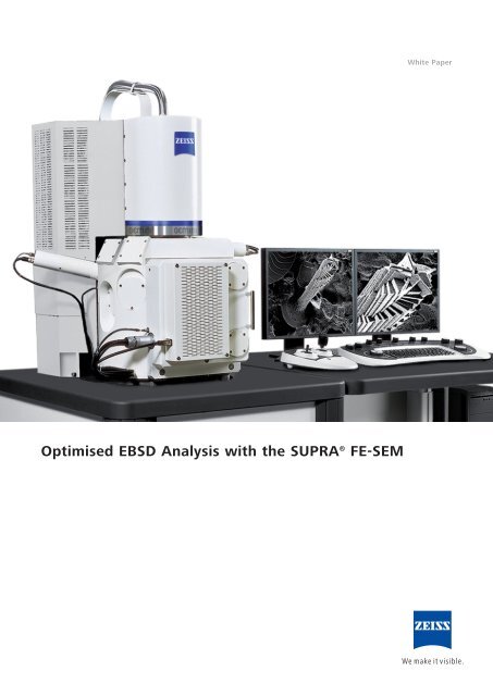
Optimised EBSD Analysis with the SUPRA® FE-SEM - Carl Zeiss
Optimised EBSD Analysis with the SUPRA® FE-SEM - Carl Zeiss
Optimised EBSD Analysis with the SUPRA® FE-SEM - Carl Zeiss
- No tags were found...

Create successful ePaper yourself
Turn your PDF publications into a flip-book with our unique Google optimized e-Paper software.
<strong>Optimised</strong> <strong>EBSD</strong> <strong>Analysis</strong> <strong>with</strong> <strong>the</strong> SUPRA ® <strong>FE</strong>-<strong>SEM</strong>White Paper
White Paper<strong>Optimised</strong> <strong>EBSD</strong> <strong>Analysis</strong> <strong>with</strong> <strong>the</strong> SUPRA ® <strong>FE</strong>-<strong>SEM</strong>Author:<strong>Carl</strong> <strong>Zeiss</strong> MicroscopyDate: March 2005IntroductionElectron Backscattered Diffraction (<strong>EBSD</strong>), also known asEBSP, BKD or OIM, is a <strong>SEM</strong> technique applicable tocrystalline materials. It provides absolute crystal orientationinformation down to <strong>the</strong> nano scale level when a dedicatedField Emission <strong>SEM</strong> is used. <strong>EBSD</strong> allows identification ofphases and discrimination between phases in materials. The<strong>EBSD</strong> patterns are produced when an electron beam strikesa specimen surface. The electron scattering in <strong>the</strong> materialcauses electrons to travel in all directions. Electrons thatsatisfy <strong>the</strong> Bragg condition, i.e. n=2d sin, for a crystalplane are channelled and show <strong>the</strong> Kikuchi bands, see fig.1.<strong>EBSD</strong> patterns were first observed by Kikuchi in a TEM. For<strong>the</strong> <strong>EBSD</strong> detection in a <strong>SEM</strong> a fluorescent phosphor screenin front of a highly sensitive CCD camera is used. The <strong>EBSD</strong>detector system is mounted on one of <strong>the</strong> side ports of<strong>the</strong> specimen chamber and should bring <strong>the</strong> fluorescentscreen close to <strong>the</strong> specimen. For clear <strong>EBSD</strong> patterns <strong>the</strong>specimen surface has to be distortion free. This can only beachieved <strong>with</strong> proper specimen preparation techniques likeelectro-polishing or using a focussed ion beam system like<strong>the</strong> CrossBeam ® .Instrumentation requirementsIn order to enable <strong>EBSD</strong> in a <strong>FE</strong>-<strong>SEM</strong>, <strong>the</strong> <strong>EBSD</strong> detector hasto be mounted on <strong>the</strong> side port of <strong>the</strong> specimen chamber.The specimen has to be tilted to 70 degrees to project <strong>the</strong>pattern on <strong>the</strong> <strong>EBSD</strong> detector. Forward scattered BSE detectorsare mounted on <strong>the</strong> <strong>EBSD</strong> detector to enable phase andZ-contrast imaging of <strong>the</strong> specimen surface. In order tocombine chemical and phase identification an EDS detectorneeds to be installed facing towards <strong>the</strong> specimen at exactly<strong>the</strong> same coincidence point as <strong>the</strong> <strong>EBSD</strong> detector.Figure 1Example of <strong>EBSD</strong> pattern.2
White PaperThe ZEISS SUPRA ® 55 and 55VP <strong>FE</strong>-<strong>SEM</strong>s both have integrateddesign features for superior <strong>EBSD</strong> analysis:■ GEMINI ® <strong>FE</strong>-<strong>SEM</strong> column supplies a highly stable electronbeam for fully automated analysis of large areas■ High Current, Depth of Field module <strong>with</strong> <strong>the</strong> virtual<strong>FE</strong> source moved to infinity (fig. 2) supplies a highlyparallel beam <strong>with</strong> a high current density enabling improvedlateral resolution (sub 10nm), high angular resolution(0.25º) and fast detection times (100 points/sec).■ Precise scan control and calculated compensation for tiltcorrection combined <strong>with</strong> dynamic focus gives distortionfree imaging, see fig.3■ Chamber geometry supplies an excellent platform forcoplanar <strong>EBSD</strong> and EDS analysis at 8.5mm WD andspecimen tilt of 70º, see fig. 4■ Eucentric specimen stage provides accurate tilt to 70ºand stability for large area automated phase detection■ Variable pressure capabilities to analyse non conductingspecimens like ceramics and semiconductors (for <strong>the</strong>SUPRA ® 55VP only)■ No magnetic field outside <strong>the</strong> GEMINI ® end lens eliminatesdistortions when analysing magnetic or para-magneticspecimensFigure 2GEMINI ®High Current mode<strong>with</strong> virtual parallel beam:optimised <strong>EBSD</strong>.Applications(courtesy of HKL Technology)<strong>EBSD</strong> analysis is an extremely useful technique for crystalorientation, phase identification (combined <strong>with</strong> EDS analysis),phase verification (like in duplex steels), texture measurement,boundary characterisation and deformation measurements.The following application examples have been provided byHTL Technology A/S, Hobro, Denmark.The instrumentation used for <strong>the</strong> <strong>EBSD</strong> analysis was <strong>the</strong>HKL Nordlys II EDSD Detector, Channel 5 software and <strong>the</strong>ZEISS SUPRA ® 55VP <strong>FE</strong>-<strong>SEM</strong>.Figure 3Undistorted geometry at 700° tilt. Tilt correction on, dynamic focus not used!3
White PaperFigure 4<strong>Optimised</strong> <strong>EBSD</strong> geometry:<strong>EBSD</strong> and EDS detectorsclose to <strong>the</strong> specimen at70 degrees tilt.ChamberSE detectorVPSE detectorRoentec SDD EDS detectorGEMINI ® end lensHKL TechnologyNordlys II <strong>EBSD</strong>detectorForescatter BSE detectorsSpecimen at 70 degrees tiltFigure 5Example of <strong>EBSD</strong>Imaging of AngariaDelphinus shell whichhas an unstable CaCO 3(aragonite) structureunder <strong>the</strong> electronbeam. <strong>EBSD</strong> patternwhere taken <strong>with</strong> aspeed of 100 patterns/sec to minimise beamdamage.5a: Fore-scatter image.5b: <strong>EBSD</strong> Band Contrast.5c: Inverse pole figurecolouring (IPF).5d: Legende for IPF(right). Arogonitecrystal structure(above).adbc4
White PaperFigure 6Example of <strong>EBSD</strong> onduplex stainless steel.6a: Fore-scatter image.6b: <strong>EBSD</strong> Map.6c: Phase map: ferritegreen/austenite blue;6d: Recrystalised blue,deformed red.adbcFigure 7SUPRA ® 55VP <strong>FE</strong>-<strong>SEM</strong><strong>with</strong> <strong>the</strong> HKL TechnologyNordlys <strong>EBSD</strong> detector.5
facebook.com/zeissmicroscopytwitter.com/zeiss_microyoutube.com/zeissmicroscopyflickr.com/zeissmicroEN_40_011_022 | CZ-05/2012 | Design, scope of delivery and technical progress subject to change <strong>with</strong>out notice. | © <strong>Carl</strong> <strong>Zeiss</strong> Microscopy GmbH<strong>Carl</strong> <strong>Zeiss</strong> Microscopy GmbH07745 Jena, Germanymicroscopy@zeiss.comwww.zeiss.com/microscopy