

MT13x9 hardware interface to front panel - ivanov.eu
MT13x9 hardware interface to front panel - ivanov.eu
MT13x9 hardware interface to front panel - ivanov.eu

Create successful ePaper yourself
Turn your PDF publications into a flip-book with our unique Google optimized e-Paper software.
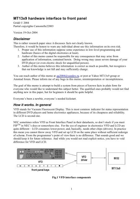
<strong>MT13x9</strong> <strong>hardware</strong> <strong>interface</strong> <strong>to</strong> <strong>front</strong> <strong>panel</strong>Gridd © 2004Partial copyrights Camomille22003Version 19-Oct-2004DisclaimerThis is rather research paper since it discusses facts not clearly known.Therefore, it would be honest <strong>to</strong> warn any individual about use this information on its own risk.1. Proper use of this information suppose some experience in low-level programming and<strong>hardware</strong> (basics of the digital electronics at least).2. Author of this memo cannot be responsible for any consequences that may arise fromapplication of information, contained herein. Doing wrong may cause severe damage of yourDVD player (or even electric shock for unqualified person).3. Author of this memo believes this information is correct as much as possible, but recognizesthat our knowledge is not full and may sufficiently change.You can reach author of this memo at gg2004@yandex.ru, or post at Yahoo <strong>MT13x9</strong> group orAmstrad forum. Please inform me of any bugs in this memo, misinterpretation or incompleteness.The goal of this memo is attempt <strong>to</strong> build a system from pieces of known facts in plain form foreveryone who would like <strong>to</strong> understand this subject better. The qualified ones probably would not findanything new in this paper, but for beginners it should be quite helpful.Everyone’s been a newbie, everyone’s needed kickstart.How it works. In generalVFD stands for Vacuum Fluorescent Display. This is most common indica<strong>to</strong>r for status representationin different DVD players and home electronics appliances, because of its cheapness and reliability.The LCD is second one.NEC sometimes refers VFD as Front Interface Panel in their datasheets, so don’t stuck if you meetFIP TM in NEC’s docs or somewhere else. For the eye of engineer in electronics VFD and LCD arequite different – LCD consumes lower power, and, basically, needs other chips (drivers). In practicethis mean you cannot throw away VFD and set up LCD on the same place without sufficient redesignof scheme. From the programmer’s point of view there is no difference. That sounds good and weshould keep it for future reference. And while you would not read explicit notice, you have <strong>to</strong> voiddifference for VFD and LCD.Fig.1 VFD <strong>interface</strong> components1
The general VFD <strong>interface</strong> is shown at Fig.1 User reads device status on display and tries <strong>to</strong> changethe sequence of operation by pressing <strong>front</strong> <strong>panel</strong> keys. A chip responsible for displaying outinformation on VFD and reading but<strong>to</strong>ns named as VFD driver. It is controlled by 8032 processor coreintegrated in <strong>MT13x9</strong>. For MT1389-based boards this IC is usually NEC ìPD 16312 or compatible(for successful datasheet search by google you have <strong>to</strong> type uPD or even mPD at search bar).MT1369-based boards use NEC ìPD 16311. MT1379 boards can use both types.Original NEC chips are not frequent guests on printed circuit boards. There is a number of VFDdrivers available on market and most of them are made by Asian manufacturers not widely known.(Prince<strong>to</strong>n Technologies (PT), HolTek (HT), SamHop MicroElectronics (SM), Topro (TP), AnaChip(AD)) But last two digits in chip model number may give some info when docs are lacking. If there are‘12’ or ‘11’ there is a chance that chip would be compatible with NEC. To ensure this, try <strong>to</strong> retrievedatasheet from the Net. You may require Chinese Acrobat Reader (or full Acrobat) for successfulreading (even if these datasheets were written in English they may use numbers and some symbolsfrom Chinese fonts J ).Variety of designsIf DVD manufacturer can spend some additional resources <strong>to</strong> improve <strong>hardware</strong> design or just <strong>to</strong>create something different and, for its opinion, cus<strong>to</strong>mer attractable, then VFD board schematics maybecame quite different of reference Mediatek design.There are some VFD boards distinctive from that reference – BBK 965S, LG 7831, Pioneer DV-470-S,Philips DVD LX-8300.BBK965S uses LCD driver PT6554LQ by Prince<strong>to</strong>n Technologies. As mentioned above, from theprogrammer’s point of view there is no difference between LCD and VFD, but PT6554LQ also differsfrom NEC uPD 16312 – it has more pins and consequently more inner registers. It looks like extendedversion of 16312 and uses other command set (but similar – none carefully checked that). Furtherexploration is needed <strong>to</strong> determine distinct features. Unfortunately, there is no complete datasheetavailable on the Net (the currently available one has pinout and examples of typical applications but itlacks of programming guide).LG 7831 uses Hynix GMS81C2012. This is programmable 8-bit MCU (microcontroller unit) and hasindependent program wired in the internal ROM. And, again, further exploration is needed. ProbablyMCU may be responsible for generation characters on chip side and therefore 8032 code of LG may besimpler <strong>to</strong> understand, since there would not be character tables inside 8032 code. But this is not a fact,just a proposition…Pioneer DV-470-S, Philips DVD LX-8300 use different VFD drivers – PE5374B and ToshibaTMP87CH74 respectively. When reversing code you have <strong>to</strong> have these datasheets at hand.Links <strong>to</strong> some datasheetsNEC uPD 16312 (you can find here uPD 16311 also)http://www.alldatasheet.com/datasheet-pdf/view/NEC/UPD16312.htmlPT6554http://www.prince<strong>to</strong>n.com.tw/english/product/getProductFile.asp?Product_no=PT65542
Hynix GMS81C2020http://www.hynix.com/eng/products/ system_ic/sp/down/GMS81C2020.pdfPE5374BUnknown chip by unknown manufacturer. No datasheet . Let author know if you find somethingabout.Toshiba TMP87CH74http://pdf.<strong>to</strong>shiba.com/taec/components/Datasheet/TMP87CH74_M74.pdfVFD in itselfVFD is fragile vacuum-contained tube with luminescent anode segments and cathode grids inside.There is a huge variety of VFDs on market since manufacturers pay enough attention <strong>to</strong> exterior viewof production. A lot of VFD manufactures are not known <strong>to</strong> wide public. The well-known names areSamsung and Futaba and more or less known are ZEC and Noritake.A good FAQ on VFD technology resides on Noritake site.http://www.noritake-elec.com/vfd_technology.htmThis is a good introduction in <strong>hardware</strong> matter. You can learn that is ‘duty fac<strong>to</strong>r’, ‘bias’ and lot ofother stuff, but this is extra reading. If you miss it, you lose almost nothing.Samsung VFD and recommended VFD drivers for their production is athttp://www.samsungsdi.co.kr/contents/en/product/vfd/vfd.htmlFind «VFD catalog», Click «View e-book»I don’t know who was that smart boy in Samsung who put PDFs in flash player. Instead of whole thing downloading you have <strong>to</strong> sit and click for everypage in VFD catalogue. That’s boring and embarrassing even on 256K link. Really!MAXIM site also has web pages of VFD tube manufacturers (some links are dead)http://www.maxim-ic.com/appnotes.cfm/appnote_number/1154Service Manuals often miss the VFD manufacturer’s name and sometimes even does not containmodel number. Therefore, understanding which information displayed at specific program point is notsimple. There is a perfect page from Grundig Xenaro GDP 5100-6150 service manual. This isextremely rare case when manufacturer puts VFD layout in manual. Grundig player does not useMT1389, but has similar VFD controller board. Fig.2 included just for reference <strong>to</strong> better understandthe connections of VFD <strong>to</strong> driver chip and how it displays information.3
Fig 2. Futaba VFD example. Model 6-BT-297GK.(from Grundig Xenaro GDP 5100-6150 service manual)This VFD has six grids (1G-6G) and 16 segments (P1-P16) connected internally <strong>to</strong> different symbolsand common 7-segment indica<strong>to</strong>rs. Other models usually have different sets. To highlight specificsymbol or digital element you have <strong>to</strong> select respective grids and segments, i.e current should bedriven <strong>to</strong> these pins by VFD driver chip.Another good example is from Philips manual. DVD players manufactured by Philips often useindica<strong>to</strong>rs capable <strong>to</strong> show any alphanumeric symbol. (15-segment) versus traditional 7-segment.4
Fig 3. Overall view of HUV-08SS57T or 20U26115TAN , with detailed view of single 15-segmentelement (from Philips LX-3900-SA service manual)Table 2. Relation between grids and segments for Philips indica<strong>to</strong>rand we should not miss excellent camomille’s drawings in Excel. It may be very useful for VFDsconsisting of 7-segment elements. (Characteres.xls 34816 bytes in size)5
VFD driverLet’s look <strong>to</strong> VFD chip closer with connected VFD Futaba 6-BT-297GK (not shown here, see fig.2)Fig 3. VFD driver example. (NEC ìPD16312)(from Grundig Xenaro GDP 5100-6150 service manual)Short pins description: (more detailed – in ìPD16312 datasheet)Pin OSC is an external oscilla<strong>to</strong>r pin required for chip synchronizing and has no interest forprogramming. Pins VSS, VDD are the supply power for IC and has no interest for programming also.Understanding of other pins is essential.VFD Futaba 6-BT-297GK has grids G1-G6 connected <strong>to</strong> 32-37 pins of VFD driver IC (GRID6-GRID1). Such signal wiring is illogical only at first glance and may be easily justified by PCB layout.This is done often <strong>to</strong> improve signal throughput, reduce noise and cross-talks between neighbor wires.Don’t forget – there are hard- and soft- wares. The PCB redesign requires much more efforts, time andmoney in comparison of changing bits order while programming.Segments of Futaba VFD connected <strong>to</strong> 15-31 pins (P16-P1 respectively). This is a set of pins(SEG1/KS1-KS6, SEG7-SEG11 and SEG12/GRID11-SEG16/GRID7). Some pins may have differentassignment, depending on selected VFD driver configuration.LED1-LED4 – each of these pins can directly connect <strong>to</strong> LED. Status of bits can be programmedindependently. Oftenly one LED used <strong>to</strong> show STANDBY status. BBK 965S uses more LED pins forLCD backlight of regulated intensity.KEY1 – KEY4 – key matrix for <strong>front</strong> <strong>panel</strong> but<strong>to</strong>ns (PAUSE, STOP, REWIND, etc.). Front keys alsowired <strong>to</strong> SW1-SW2 (not shown on Fig.3) but Grundig <strong>front</strong> <strong>panel</strong> is not suitable for educational7
purposes (engineers drawn jog dial and but<strong>to</strong>ns which were not seen at <strong>front</strong>). So we should look forsome primitive circuit <strong>to</strong> learn basics. Here is it.Fig.4. Keyscan Matrix example(from Memorex MD2028 Service Manual (MT1379))Some wirings were removed <strong>to</strong> clean the picture (pin 14, for example). Note the STANDBY LED onLED0 (pin 42). There is a plain set of <strong>front</strong> <strong>panel</strong> but<strong>to</strong>ns, connected <strong>to</strong> KEY0-KEY3 (rows) and SG1-SG3 (columns). To read the status of pressed but<strong>to</strong>n, you should select respective column by settingone of SG1-SG3 <strong>to</strong> ‘1’. Current began <strong>to</strong> flow and if but<strong>to</strong>n pressed it goes <strong>to</strong> respective KEY0-KEY3input. VFD driver reads status and s<strong>to</strong>res bits for each pressed but<strong>to</strong>n in internal RAM register.And, again, this is a just an example. In most cases of real life, circuit diagrams of specific players willbe different.To cus<strong>to</strong>mize VFD driver chip for handling miscellaneous numbers of grids and segments, the chipshould be programmed appropriately. Basically driver chip configuration (number of supported SEGsand GRIDs) programmed only once during initial setup. It may use default settings also.VFD <strong>interface</strong> <strong>to</strong> host. 4-wire vs. 3There is a detailed description of the internal VFD driver registers in datasheets, consequently there isno need <strong>to</strong> copy manual pages here. You can always download and read original.Nevertheless, some attention <strong>to</strong> programming of chips should be paid. Usually this <strong>to</strong>pic is not coveredextensively and datasheets are full of technical details useful for engineers in electronics but have littleinterest for programmers.VFD driver gets commands and puts data <strong>to</strong> host by DIN / DOUT / CLK / STB serial <strong>interface</strong>(Sometime it refers as NEC <strong>interface</strong>). Let’s look closely at VFD driver from previous figure 4.8
Fig.5 A closer view <strong>to</strong> host <strong>interface</strong>.(from Memorex MD2028 Service Manual (MT1379))Table1. NEC <strong>interface</strong> pinsName on Name on Name on Purposechip connec<strong>to</strong>r MT1389DINVFD driver data inputDAT VDATADOUTVFD driver data outputCLK CLK VCLK VFD driver tx/rx data clockCS (STB) STB VSTB Chip select (strobe)Flat cable, connected <strong>to</strong> CN1 at fig.5 leads <strong>to</strong> MPEG board where these signals connect <strong>to</strong> MT1389(8032 host) pins. Signal may change its name when traveling between sheets of drawings andcomplicate understanding for the first time. That happens very frequently because OEM servicemanuals created by copying and pasting pages from different sources and none carefully scrutinizesevery sheet.Originally NEC proposed 4-wire <strong>interface</strong>. Basically, there is no simultaneous read/write operationsfrom/<strong>to</strong> VFD driver at the same time. To reduce number of wires, pins DIN and DOUT are usuallysoldered <strong>to</strong>gether. Chip inside has some protective logics preventing registers data from mutualinfluence. Thus, 4 wires became 3.To see which pins of MT1389 used for VFD <strong>interface</strong>, look at the summary table at the end of thismemo. Note the ‘shifting up and wrapping around’ of VFD <strong>interface</strong> bits in MT1369 devices, and nodifference between MT1379 and MT1389.As we can see, DVD manufacturer for some purpose may change assignment of 8032 bits <strong>to</strong> controlVFD driver. This is one of the reasons why firmwares may be incompatible between OEMs and maynot work if flashed directly without adaptation.Adaptation requires careful studying of all available info. The best source is service manual forspecific model, but obtaining it is not simple, and frequently is not possible.And even you have pdf on hand, be careful. For example, schematics of BBK965S probably may haveerrata. Circuit Diagram of VFD board shows separated DIN and DOUT wires, but MPEG board get9
only one – VSDA. For proper functioning it should be somewhere connected <strong>to</strong>gether, but this is notshown.The known exclusions of VFD design are LG 7831, Pioneer DV-470-S, Philips LX-3900. They usedifferent chips as VFD drivers. (Philips and LG use MCU, Pioneer uses unknown chip)Serial Communication Format for NEC 16311/16312 and compatiblesNevertheless, number of players (especially non-brands) has NEC-compatible chips.Fig.6 Data reception over NEC <strong>interface</strong>.(snatched from NEC mPD 16312 datasheet)Reception is for VFD driver side, for 8032 side it would be transmission. To write data we should:1. Set STB pin low.2.Put data on DIN,3.Accompany each bit with <strong>to</strong>ggling CLK.….. < if command requires additional data,serialize bytes <strong>to</strong> bitsand send them across the wire>4. set STB pin high.VFD <strong>interface</strong> pin arrangement for BBK965SP13 – VSCK (CLK)P14 – VSDA (DIN/DOUT)P15 – VSTB (STB)The following code (CODE4:A373 – CODE4:A37D) from BBK965S firmware bank4, an example ofsending command <strong>to</strong> VFD <strong>interface</strong>. The ‘???’ shows that 0x43 is doubt <strong>to</strong> be ‘SCAN KEYS’ J, butin this case, it does not matter.10
Fig.7 Example code for complete <strong>interface</strong> cycle <strong>to</strong> VFD from 8032 (BBK 965S)To see what happened in detail we should look transmit_byte_<strong>to</strong>_VFD subroutine listing:Fig.8 Example code for byte transmission <strong>to</strong> VFD from 8032 (BBK 965S)and its relation <strong>to</strong> signal timings11
VSTB(STB) stay low all the time while data transmission is in progress. VFD reads VSDA(DIN) onthe rising edge VSCLK(CLK) (transition from low <strong>to</strong> high – ‘setb P13’). The order of bits intransmission is from LSB <strong>to</strong> MSB (serialization and output done by ‘rrc A / mov P14,C’ commands).Fig. 9. Data transmission over NEC <strong>interface</strong>(snatched from NEC mPD 16312 datasheet)And again transmission is for VFD driver side, for 8032 it would be reception.To read data we should:1. set STB low and keep it while reading is not completed.2. <strong>to</strong>ggle CLK from high <strong>to</strong> low (falling edge)3. read data from DIN/DOUT,4. set STB high when reading has <strong>to</strong> be completed <strong>to</strong> close serial <strong>interface</strong>.LSB goes first when 8032 reads VFD driver. Between sequential write and read there should be delayof twait <strong>to</strong> ensure write operation has been completed and there would not be unwanted influence ofprevious operation. Datasheet says that 1 microsec of delay would be enough. Usually you see the sixor seven nops in code.After this discussion understanding of display memory updating by incrementing address would bequite obvious. Note the behaviour of STB signal. It <strong>to</strong>ggles every new command and stays low whilecommand data (DIN) are transmitting. You cannot transmit more than 22 bytes between STB <strong>to</strong>ggles.This is NEC 16312 chip restriction.Fig.10 Updating display memory by incrementing address.(snatched from NEC mPD 16312 datasheet)12
Fig. 11. updating specific adress.(snatched from NEC mPD 16312 datasheet)Happy reversing!Gridd, 19.10.200413
DaewooDVG-8500N(HitachiHOP1120/1200)MemorexMVD2029(Sony KHM-234)PhilipsDVD625(submods /001/021 /051),PhilipsDVD728/729/731Table 2. Summary Table (from unpublished paper)Sanyo SF-HD60AV(MemorexMVD2028 /2030)MemorexMVD2022 ,POLARDV10xx,(Sony KHM-280)BBK965SMTK Refdesign boardPhilipsLX3900SA(mod.01/05/69/75/93)PhilipsDVD LX-8300 (mod.PioneerDV-470-S/KLG DV8731Processor MT1369AE MT1369E MT1379E MT1379E MT137E ‘C’ MT1389 MT1389 MT1389E MT1389E MT1389EE MT1389 ProcessorP1.0 ? ? ? ? ? ? ? ? ? ? P1.0P1.1 ? ? ? ? ? ? ? ? ? ? P1.1P1.2 VSTB VSTB STBY_DECT No conn No conn no conn no conn No conn No conn FP_SO no conn P1.2P1.3 VSCK VSCK VSCK VSCK VSCK VSCK VSCK VSCK VSCK FP_SCK No conn P1.3P1.4 VSDA VSDA VSDA VSDA VSDA VSDA VSDA VSDA VSDA FP_ACK VFD_SCK P1.4P1.5 STANDBY ASTB VSTB VSTB VSTB VSTB VSTB VSTB Selection FP_SI VFD_TXD P1.5HDMI/DACP1.6 SCL (I 2C) SCL SCL SCL SCL SCL SCL SCL SCL_HDMI SCL SCL P1.6(SCL_DAC)P1.7 SDA (I 2C) SDA SDA SDA SDA SDA SDA SDA SDA_HDMI SDA SDA P1.7(SDA_DAC)P3.0 MICMUTE P3.0 1 ASTB TV1 P3.0 ASTB No conn No conn STB_SW FP_IRQ LIMIT No conn P3.0P3.1 MUTE P3.1 P3.1 TV2 P-S-SELECT No conn No conn AV_MUTE AV_MUTE UP3_1 VFD_RXD P3.1P3.2 ? ? ? ? ? ? ? ? ? ? ? P3.2P3.3 ? ? ? ? ? ? ? ? ? ? ? P3.3P3.4 RXD RXD RXD RXD RXD RXD RXD RXD RXD RXD RXD P3.4P3.5 TXD TXD TXD TXD TXD TXD TXD TXD TXD TXD TXD P3.5Front <strong>panel</strong>controllerNEC uPD16311NEC uPD16311NW 6312(625), PT6312(728-731)PT6312 orHR6319 orHT16512Unknown(Missing pages)PT6554LQ NW6312 NW6312PT3611uPD16311 2TMP87CH74PE5374BHynixGMS81C2012Parentalpassword3308 7890 ParentalpasswordDesign name Not specified MTK_1369_HD6_E2T4 3625 - CL36532022_015(19/03/03)728-729-731 –(27/03/03)MT1379SERVO SONYMEGANot specified CONF_V2 SD6.1 SD6.3 WYXCN,WYxCN/FGDV8000’SSR14811BDesignnameMTK_1369_HD6Revisions:E1T2 -MVD2028E1T3 -MVD2030Front<strong>panel</strong>controller? – Not known from schematicsNo conn – No connection1 This is not a mistyping, all the names are from circuit diagram2 A bit confusing – NW6312 and mPD16311 written <strong>to</strong>gether on schematics, at block diagram PT3611 specified (typo?)3 Looks like design for Sanyo14


