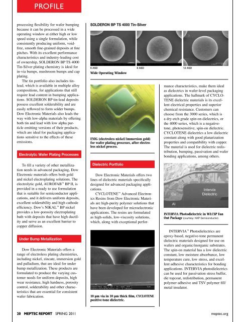
PROFILEprocessing flexibility for wafer bumpingbecause it can be processed in a wideoperating window at either high or lowspeed using a single formulation, whileconsistently producing uniform, voidfree,smooth fine-grained deposits at finepitches. With its excellent performancecharacteristics and industry-leading costof ownership, SOLDERON BP TS 4000Tin-Silver plating chemistry is ideal forin-via bumps, mushroom bumps and capplating.The tin portfolio also includes tinlead,which is available in multiple alloycompositions, for applications that stillrequire lead content in bumping applications.SOLDERON BP tin-lead depositspossess excellent solderability and areeasily reflowed to form solder bumps.Dow Electronic Materials also leads theway with low-alpha materials by offeringboth tin and lead with low alpha particleemitting versions of their products,which are ideal for packaging applicationssensitive to the effects of theseemissions.Electrolytic Wafer Plating ProcessesTo fill a variety of other metallizationneeds in advanced packaging, DowElectronic materials offers both goldand nickel electroplating solutions. Theelectrolytic gold, AUROFAB BP II, isprovided in a ready to use formulationthat is suitable for semiconductor applications,and it delivers uniform deposits,excellent solderability and high cathodeefficiency. Dow’s NIKAL BP nickelprovides a low-porosity electroplatingbath with deposits that have high ductilityand serve as an excellent barrier tocopper diffusion.Under Bump MetallizationDow Electronic Materials offers arange of electroless plating chemistries,including nickel, zincate, immersion goldand palladium, that are ideal for underbump metallization. These products areformulated to produce the varying customerneeds for uniform deposits, highwear resistance, high hardness, porositycontrol, solderability and other characteristicsthat are essential for consistentwafer fabrication.SOLDERON BP TS 4000 Tin-Silver6 ASDWide Operating WindowENIG (electroless nickel/immersion gold)for wafer plating processes, after electrolessnickel process.Dielectric Portfolio8 ASDDow Electronic Materials offers twolines of dielectric materials specificallydesigned for advanced packaging applications.CYCLOTENE Advanced ElectronicsResins from Dow Electronic Materialsare high-purity polymer solutions thathave been developed for microelectronicapplications. The resins are formulatedas high-solids, low-viscosity solutions,which, along with exceptional perfor-10 μm via in 10 μm thick film, CYCLOTENEpositive-tone dielectric.12 ASDmance characteristics, make them idealas dielectrics in wafer-level packagingapplications. The hallmark of CYCLO-TENE dielectric materials is its excellentelectrical properties and superiorchemical resistance. Customers canchoose from the 3000 series, which isa dry-etch grade spin-on dielectrics, orthe 4000 series, which is a negativetone,photosensitive, spin-on dielectric.CYCLOTENE dielectrics a low dielectricconstant along with good planarizationproperties and compatibility with copper.The material is used for dielectric redistribution,bumping, passivation and waferbonding applications, among others.INTERVIA Photodielectric in WLCSP FanOut Package (courtesy: NXP Semiconductor)INTERVIA Photodielectrics areepoxy-based, negative-tone permanentdielectric materials designed for use onwafers and organic/inorganic substrates.The spin-on material has a low dielectricconstant, low moisture absorbance, lowtemperature cure, low stress, and excellentadhesive characteristics for bondingapplications. INTERVIA photodielectricscan be used for passivation stress buffer,die topcoat, redistribution, permanentpolymer adhesive and TSV polymer fill/metal insulator.20 MEPTEC REPORT SPRING 2011 meptec.org
OPT OSEM, for a l y our OP EN CAVIT Y pack ages .OPT OSEM, for a l y our OP EN CAVIT Y pack ages .In Association WithA S P E C I A L T W O - D A Y T E C H N I C A L S Y M P O S I U MCorporate SponsorsMedia SponsorsMEMSAssociation Sponsor ASU Sponsorpage 14HOME ABOUT MEPTEC CONTACT US ADVISORY BOARD INDUSTRY PARTNERSA Quarterly Publication of The Microelectronics Packaging & Test Engineering Council Volume 15, Number 1MEMS -DRIVING INNOVATIONExisting Technologies EnableFuture Innovationspage 12World Class Manufacturing Services forPower Management Semiconductorspage 14INSIDE THIS ISSUEMEPTEC Fall EventsSingle DigitQFN PackagingThe Re-BirthTackled PackagingGrowth for TotalAdvances withof SiliconChallenges for ICsSemiconductorRoutable HighInterposers?and MEMS Devices Sales in 2011 Density Leadframe4 6 12 Technology 14SPRING 2011 MEPTEC Report 3SPRING 2011OPT OSEM, for a l y ou r OP EN CAVIT Y pack ag es .A Quarterly Publication of The Microelectronics Packaging & Test Engineering Council Volume 15, Number 1INSIDE THIS ISSUEMEPTEC Fall EventsTackled PackagingChallenges for ICsSingle DigitGrowth for TotalSemiconductorSales in 201112MEDIA SPONSORSQFN PackagingThe Re-BirthAdvances withof SiliconRoutable HighInterposers?Density LeadframeSPRING 2011 MEPTEC Report 3A SPECIAL ONE-DAY TECHNICAL SYMPOSIUMPresented byA O N E - D A Y T E C H N I C A L S Y M P O S I U M & E X H I B I T SPresenting Companies:GOLD SPONSORSOPT OSEM, for a l y our OP EN CAVIT Y pack ages .In Association WithMEPTEC&SMTAPRESENTMicroelectronics Packaging & Test Engineering CouncilSurface Mount Technology AssociationA SPECIAL TWO-DAY TECHNICAL SYMPOSIUMA SPECIAL ONE-DAY TECHNICAL SYMPOSIUMPresented bySILVER SPONSORM A Y 2 0 , 2 0 1 0 • S A N J O S E , C A L I F O R N I AA SPECIAL ONE-DAY TECHNICAL SYMPOSIUMASSOCIATION SPONSORSTAP TIMES ®Packaging PhotoresistAvailable as positive- andnegative-tone resists, INTER-VIA 3D Photoresists areaqueous-based emulsions thatcan be electrodeposited ontoa wide variety of electricallyconductivesubstrates. Theconformal properties of theseresists make them ideal forsubstrates with complexgeometries. The resists haveexceptional chemical resistanceto plating and etchingsolutions. They are designedfor wafer, MEMs, leadframes and three-dimensionalphotolithography applications.INTERVIA 3D Photoresist,25 μm lines over 45 μm highfeatures. (courtesy: IZM Fraunhofer)INTERVIA 3D Photoresist overtopography(courtesy: IZM Fraunhofer)Assembly MaterialsAs the semiconductorindustry approaches the limitationsof Moore’s law, DowElectronic Materials recognizesthe industry need forinnovative material solutionscapable of meeting challengesof achieving reliabilityfor large die with low-kmeptec.organd ultra-low-k layers. Forthat reason, Dow ElectronicMaterials is developingunderfill material solutionsfor flipchip and 3D packagingin collaboration withleading industry partners.The new materials are aimedat addressing many of thethermal and mechanical challengesinherent in increaseddie size and 3D packaging.According to Dr. JeffCalvert, director of R&D forAdvanced Packaging Technologies,progress on theseunderfill development programshas been enhanced bythe combination of the legacyRohm and Haas ElectronicMaterials with The DowChemical Company. “OurAdvanced Packaging Technologiesbusiness now hasaccess to much deeper analyticaland R&D capabilitiesas well as to a wider range ofmaterial technology options.”says Calvert. “Combining thestrengths of Rohm and Haaswith Dow together with closecustomer partnerships hasbeen powerful.”As semiconductor technologyfor front end andback end packaging andassembly converges, materialsand material interactionsbecome more complex.According to Bhavesh Muni,global marketing manager forAssembly Materials, “Dowis uniquely positioned tooffer complete integratedpackaging material solutionsfor the next-generation ofsemiconductor packages withour in-depth understandingand product offerings in thesemiconductor front-end, ourgrowing portfolio of backendproducts, and our focuson innovation in material science.”For more informationabout Dow Electronic Materialsand the advanced packagingportfolio, visit www.dow.com or contact BhaveshMuni at bmuni@dow.com.◆OPTOSEM, forall yourOPEN CAVITYMicroelectronics Packaging & Test Engineering CouncilWelcome to the Next GenerationWELCOMEMEPTEC&SMTAPRESENTMicroelectronics Packaging & Test Engineering CouncilSurface Mount Technology Association2010MedicalElectronicsSymposiumSuccessful Strategies for theMedical Electronics SectorWednesday & ThursdaySeptember 22nd & 23rdOutput (1) @ 100% of File Size • Final Size 31.5” x 79.75”QFN forMEMSAPPLICATION in Proximity Switches, RF Components, OpticalFinger Navigation, Microphones and other MEMS SensorsOPTOSEM TECHNOLOGIES SDN BHD was established in Johor, Malaysiain 2002. The company specializes in the design and molding of Open Cavity ICPackages. Development in Injection Molding of QFN packages open up themarket for MEMS and other Open CavityTel : 607-3531953, 3541951products and application, and creating newFax: 607-3535420opportunities and solution for its customers, and Email :scteoh@optosem-tech.comthe market.james.chua@optosem-tech.cometkoh@optosem-tech.comwww.optosem-tech.com-DRIVING INNOVATIONExisting Technologies EnableFuture Innovationspage 12Microelectronics Packaging & Test Engineering CouncilQuarterly Technical SymposiumsWorld Class Manufacturing Services forMonthly Power Management Luncheons Semiconductors4and MEMS Devices6MEPTECPRESENTSMicroElectronics Packaging and Test Engineering Council8th AnnualMEPTEC8th AnnualMEPTECMEMS SymposiumMEMS and IC System Integration:From Sensing to AwarenessS A N J O S E • C A L I F O R N I A5.20.102010Medical ElectronicsSymposium / Day OneSuccessful Strategies for theMedical Electronics SectorASU CAMPUS • TEMPE • ARIZONA9.22.10MEMS SymposiumSemiconductorMEMS and IC System Integration: PackagingFrom Sensing to Awareness Roadmaps• Amkor Technology• Analog Devices• Fraunhofer Institute forSilicon Technology (ISIT)• Fullpower Technologies• IMEC• Intel Corporation• IntelliSense• MEMS Industry GroupApplications Driving Requirements• Roger Grace AssociatesS A N T A C L A R A • C A L I F O R N I A• Sandia National Laboratories• Silicon Clocks• SVTC 11.10.10• University of Californiaat Berkeley• WiSpry, Inc.• Yole DéveloppementQuarterly Symposiums. Monthly Luncheons. Industry Networking.Promotion & Marketing. Sponsorship & Exhibiting Opportunities.2011 Media Kit Now Available at www.meptec.orgTechnology 14SPRING 2011S A N J O S E • C A L I F O R N I APresented by2.25.10SPRING 2011 MEPTEC REPORT 21Original Image Courtesy Sandia National Laboratories