AX3484 3A, 23V, 340kHz Synchronous Rectified Step-Down ...
AX3484 3A, 23V, 340kHz Synchronous Rectified Step-Down ...
AX3484 3A, 23V, 340kHz Synchronous Rectified Step-Down ...

Create successful ePaper yourself
Turn your PDF publications into a flip-book with our unique Google optimized e-Paper software.
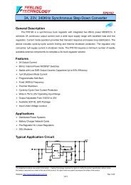
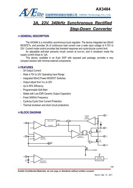
<strong>AX3484</strong><strong>3A</strong>, <strong>23V</strong>, <strong>340kHz</strong> <strong>Synchronous</strong> <strong>Rectified</strong> GENERAL DESCRIPTION<strong>Step</strong>-<strong>Down</strong> ConverterThe <strong>AX3484</strong> is a monolithic synchronous buck regulator. The device integrates two 85mΩMOSFETs, and provides <strong>3A</strong> of continuous load current over a wide input voltage of 4.75V to<strong>23V</strong>. Current mode control provides fast transient response and cycle-bicycle current limit.An adjustable soft-start prevents inrush current at turn-on, and in shutdown mode thesupply current drops to 1μA.This device, available in an 8-pin SOP with exposed pad package, provides a verycompact solution with minimal external components. FEATURES- <strong>3A</strong> Output Current- Wide 4.75V to <strong>23V</strong> Operating Input Range- Integrated 85mΩ Power MOSFET Switches- Output adjust from V FB to 20V- Up to 95% Efficiency- Programmable Soft-Start- Stable with Low ESR Ceramic Output Capacitors- Fixed 340KHz Frequency- Cycle-by-Cycle Over Current Protection- Thermal shutdown and short circuit protections BLOCK DIAGRAMFB50.3V+-OSCILLATOR90/340KHzRAMPCLKCURRENTSENSEAMPLIFIER+-5V2 IN1 BSSS70.925V-++ERRORAMPLIFIER6μA+-SRCURRENTCOMPARATORQQM185mΩM285mΩ3SW4GNDENINEN 67VZener1.5V+-SHUTDOWNCOMPARATORINTERNALREGULATORS5V1/6Axelite Confidential Materials, do not copy or distribute without written consent.Rev.0.2 Mar. 01, 2011
<strong>AX3484</strong> PIN ASSIGNMENTThe package of <strong>AX3484</strong> is SOP-8L-EP; the pin assignment is given by:( Top View )BS18SSINSW2<strong>3A</strong>XGND76ENCOMPGND45FBSOP-8L-EPNameDescriptionHigh-Side Gate Drive Boost Input. BS supplies the drive for the high-side N-ChannelBS MOSFET switch. Connect a 0.01μF or greater capacitor from SW to BS to power the highside switch.Power Input. IN supplies the power to the IC, as well as the step-down converter switches.IN Drive IN with a 4.75V to <strong>23V</strong> power source. Bypass IN to GND with a suitably largecapacitor to eliminate noise on the input to the IC. See Input Capacitor.Power Switching Output. SW is the switching node that supplies power to the output.SW Connect the output LC filter from SW to the output load. Note that a capacitor is requiredfrom SW to BS to power the high-side switch.GND Ground.Feedback Input. FB senses the output voltage to regulate that voltage. Drive FB with aFB resistive voltage divider from the output voltage. The feedback threshold is 0.925V. SeeSetting the Output Voltage.Compensation Node. COMP is used to compensate the regulation control loop. Connect aseries RC network from COMP to GND to compensate the regulation control loop. In someCOMPcases, an additional capacitor from COMP to GND is required. See CompensationComponents.Enable Input. EN is a digital input that turns the regulator on or off. Drive EN high to turnENon the regulator, drive it low to turn it off. Pull up with 100kΩ resistor for automatic startup.Soft-Start Control Input. SS controls the soft start period. Connect a capacitor from SS toSS GND to set the soft-start period. A 0.1μF capacitor sets the soft-start period to 15ms. Todisable the soft-start feature, leave SS unconnected.Axelite Confidential Materials, do not copy or distribute without written consent.2/6Rev.0.2 Mar. 01, 2011