792 GB 170 - 373 CTV - Fusibles y Semiconductores Profesionales
792 GB 170 - 373 CTV - Fusibles y Semiconductores Profesionales
792 GB 170 - 373 CTV - Fusibles y Semiconductores Profesionales

You also want an ePaper? Increase the reach of your titles
YUMPU automatically turns print PDFs into web optimized ePapers that Google loves.
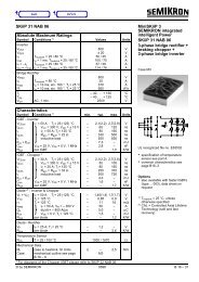
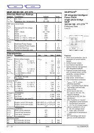
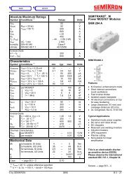
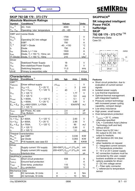
SKiiP <strong>792</strong> <strong>GB</strong> <strong>170</strong> - <strong>373</strong> <strong>CTV</strong>Absolute Maximum RatingsSymbol Conditions 1) Values UnitsV 4) isol AC, 1min 4000 VT op ,T stg Operating / stor. temperature -25...+85 °CI<strong>GB</strong>T and Inverse DiodeV CES <strong>170</strong>0 V5)V CC Operating DC link voltage 1200 VI C I<strong>GB</strong>T 750 AT 3) j I<strong>GB</strong>T + Diode -40...+150 °CI F Diode 750 AI FM Diode, t p < 1 ms 1500 AI FSM Diode, T j = 150 °C, 10ms; sin 6480 AI 2 t (Diode) Diode, T j = 150 °C, 10ms 210 kAs 2DriverV S1 Stabilized Power Supply 18 VV S2 Non-stabilized Power Supply 30 Vf smax Switching frequency 11,0 kHzdV/dt Primary to secondary side 75 kV/µsCharacteristicsSymbol Conditions 1) min. typ. max. UnitsI<strong>GB</strong>T 11)V (BR)CES Driver without supply ≥V CES − − VI CES V GE = 0, T j = 25 °C − − 3 mAV CE = V CES T j = 125 °C − 45 − mAV TO T j = 125 °C − − 1,77 Vr T T j = 125 °C − − 5,5 mΩV Cesat I C = 600A, T j = 125 °C − − 5,1 VV Cesat I C = 600A, T j = 25 °C − − 3,85 VE on + E off V CC =900/1200V, I C =750AT j = 125 °C− − 634/976 mJC CHC per Phase, AC side − 2,4 − nFL CE Top, Bottom − 2,5 − nHInverse Diode 2)V F = V EC I F = 600A; T j = 125 °C − − 2,60 VV F = V EC I F = 600A; T j = 25 °C − − 2,90 VE on + E off I F = 750A; T j = 125 °C − − 90 mJV TO T j = 125 °C − − 0,90 Vr T T j = 125 °C − − 1,8 mΩThermal Characteristics10)R thjs per I<strong>GB</strong>T − − 0,030 K/W10)R thjs per Diode − − 0,083 K/W6,10)R thsa P16 heatsink; see case S3 − − 36 K/KWDriverI S1 Supply current 15V-supply 260+590*f s /f smax +1,3*I AC /A mAI S2 Supply current 24V-supply 200+430*f s /f smax +1,0*I AC /A mAt interlock-driver Interlock-time 3,0 µsSKiiPPACK protectionI TRIPSC Short circuit protection 938 AI TRIPLG Ground fault protection - AT TRIP Over-temp. protection 115 °CU 9) DCTRIP U DC -protection 1225 VMechanical DataM1 DC terminals, SI Units 4 − 6 NmM2 AC terminals, SI Units 8 − 10 NmSKiiPPACK ®SK integrated intelligentPower PACKhalfbridgeSKiiP<strong>792</strong> <strong>GB</strong> <strong>170</strong> - <strong>373</strong> <strong>CTV</strong> 7,9)Preliminary DataCase S3Features• Short circuit protection, due toevaluation of current sensorsignals• Isolated power supply• Low thermal impedance• Optimal thermal managementwith integrated heatsink• Pressure contact technologywith increased power cyclingcapability, compact design• Low stray inductance• High power, small losses• Over-temperature protection1)2)3)4)5)6)7)8)9)10)T heatsink = 25 °C, unlessotherwise specifiedCAL = Controlled Axial LifetimeTechnology (soft and fast)without driverDriver input to DC link /AC output to DC link / ACoutput to heatsinkwith Semikron-DC link (lowinductance)other heatsinks on requestC - Integrated current sensorsT - Temperature protectionV - 15 V or 24 V power supplyAC connection busbars must beconnected by the user; copperbusbars available on requestoptions available for driver:U - DC link voltage senseF – Fiber optic connector“ s ” referenced to temperaturesensor©by SEMIKRON 0898 B 7 − 61
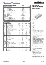
PIN-array - halfbridge driver SKiiPPACK 3-fold type “<strong>GB</strong>”X1:Pin signal remark1 shield connected to GND, when shielded cable is used2 BOT IN 4) positive 15V CMOS logic; 10 kΩ impedance,don´t connect when using fiber optic3 ERROR OUT 1) LOW = NO ERROR; open Collector Output;max. 30 V / 15 mAdon´t connect when using fiber optic,propagation delay 1 µsmin. pulsewidth error-memory-reset 8 µs4 TOP IN 4) positive 15V CMOS logic; 10 kΩ impedancedon´t connect when using fiber optic5 Overtemp. OUT 1) LOW = NO ERROR = ϑ DCB < 115 + 5°Copen collector Output; max. 30 V / 15 mA„low“ output voltage < 0,6 V„high“ output voltage max. 30 V6 + 24 V DC IN 24 V DC (20 - 30 V)7 + 24 V DC IN don´t supply with 24 V, when using + 15 V DCINsupply voltage monitoring threshold 19,5 V8 + 15 V DC IN 15 V DC + 4 %9 + 15 V DC IN don´t supply with 15 V, when using + 24 V DCINsupply voltage monitoring threshold 13 V10 GND GND for power supply and11 GND GND for digital signals12 Temp. analog OUT orU DC analog OUT 2)U DC when using option “U”actual DC-link voltage, 9 V refer to U DCmaxmax. output current 5 mA; overvoltage trip level 9 V13 GND aux 3) GND for analog signals14 I analog OUT current actual value; 8,0 V refer to I C @ 25 °Covercurrent trip level 10 V ⇔ 125 % I C @ 25 °Ccurrent value > 0 ⇔ SKiiP is sourcecurrent value < 0 ⇔ SKiiP is sinkX10: halfbridge 1 (HB1) OUTPin Signal12X11: halfbridge 2 (HB2) OUTPin Signal1 Temp.-Sensor (HB2)12 Temp.-Sensor (HB2)2X12: halfbridge 3 (HB3) OUTPin Signal128 Collector TOP (HB1)8 Collector TOP (HB2)8 Collector TOP (HB3)11 Gate TOP (HB1)12 Emitter TOP (HB1)13 Collector BOT (HB1)11 Gate TOP (HB2)12 Emitter TOP (HB2)13 Collector BOT (HB2)11 Gate TOP (HB3)12 Emitter TOP (HB3)13 Collector BOT (HB3)16 Gate BOT (HB1)17 Emitter BOT (HB1)16 Gate BOT (HB2)17 Emitter BOT (HB2)16 Gate BOT (HB3)17 Emitter BOT (HB3)type “GAL”as type “<strong>GB</strong>” except- PIN X1-4: connect this pin to GND- TOP switch does not existtype “GAR”as type “<strong>GB</strong>” except- PIN X1-2: connect this pin to GND- BOTTOM switch does not exist1)Open collector output, external pullup resistor necessary2)When using option “U” the analogtemperature signal is not available3)GND aux = reference for analogoutput signals4)„high“ (min) 11,2 V„low“ (max) 5,4 V© by SEMIKRON 0898 B 7 – 11
Case S3SKiiPPACK 3 - <strong>GB</strong>; GDWeight without heatsink: 2,72 kgP16: 6,6 kgSKiiPPACK 3 - <strong>GB</strong> with F-optionB 7 – 3 0898 © by SEMIKRON