Femtosecond-laser interactions with transparent ... - Mazur Group
Femtosecond-laser interactions with transparent ... - Mazur Group
Femtosecond-laser interactions with transparent ... - Mazur Group

You also want an ePaper? Increase the reach of your titles
YUMPU automatically turns print PDFs into web optimized ePapers that Google loves.
Table of ContentsAbstractTable of ContentsList of FiguresList of TablesAcknowledgementsCitations to Published Workiiiivviviiiixxii1 Introduction 11.1 Comparing free space and fiber propagation . . . . . . . . . . . . . . . . . . 71.2 Organization of the dissertation . . . . . . . . . . . . . . . . . . . . . . . . . 102 History of micromachining 123 Micromachining <strong>laser</strong> systems 213.1 Extended cavity oscillator . . . . . . . . . . . . . . . . . . . . . . . . . . . . 213.2 Other <strong>laser</strong> systems . . . . . . . . . . . . . . . . . . . . . . . . . . . . . . . . 293.3 Outlook . . . . . . . . . . . . . . . . . . . . . . . . . . . . . . . . . . . . . . 314 Waveguides characteristics 344.1 Refractive index measurements . . . . . . . . . . . . . . . . . . . . . . . . . 344.2 Refractive index profiles . . . . . . . . . . . . . . . . . . . . . . . . . . . . . 394.2.1 Near field mode . . . . . . . . . . . . . . . . . . . . . . . . . . . . . . 414.2.2 Discussion of index of refraction profiles . . . . . . . . . . . . . . . . 424.3 Optical transmission loss measurements . . . . . . . . . . . . . . . . . . . . 474.3.1 Transmission loss . . . . . . . . . . . . . . . . . . . . . . . . . . . . . 474.3.2 Numerical aperture from divergence measurements . . . . . . . . . . 504.3.3 Bending loss . . . . . . . . . . . . . . . . . . . . . . . . . . . . . . . 524.3.4 Scattering loss . . . . . . . . . . . . . . . . . . . . . . . . . . . . . . 534.3.5 Conclusion . . . . . . . . . . . . . . . . . . . . . . . . . . . . . . . . 55iv
List of Tables2.1 Overview of devices manufactured by femtosecond <strong>laser</strong> micromachining. . . 203.1 Damage intensity threshold for various materials <strong>with</strong> different bandgaps. . 223.2 Currently available alternative <strong>laser</strong>s used for micromachining. . . . . . . . 314.1 Various techniques used to measure the refractive index profile of femtosecond<strong>laser</strong> micromachined waveguides. . . . . . . . . . . . . . . . . . . . . . . . . 364.2 Estimates for the number of pulses irradiating a focal spot when the sampleis translated at constant speed. . . . . . . . . . . . . . . . . . . . . . . . . . 446.1 List of different technologies used for manufacturing sub-micrometer dimensiondevices. . . . . . . . . . . . . . . . . . . . . . . . . . . . . . . . . . . . . 737.1 Definitions of parameters used in Equation (7.8). . . . . . . . . . . . . . . . 977.2 Physical parameters relevant to the propagation of intense 800-nm <strong>laser</strong>pulses in different diameter fibers. . . . . . . . . . . . . . . . . . . . . . . . 110viii
Acknowledgements“I would like to put each and everyone one of you in my pocket”Nelson Mandela – 1996.There are a lot of people who have secretly contributed to me being able to writethis.From deciding to come to the US, to choosing Harvard, to living outside the lab,to working inside a lab.Perhaps the people who made the largest sacrifices have beenmy parents. In my almost six years here, I have never felt anything but love from them,constantly reinstating that they were there for me, no matter what. I have to thank mybrother for, in his succinct way, always putting things in perspective. I hope he will forgivemy inability to handle Harvard’s first year when he was in the US.But no matter what I preach, I have friends outside the lab. I don’t believe theywill ever read this, but I would like to leave it registered that I would not have enjoyed lifehere were it not for the gang from Jamaica Plain, for Lisa and Henry, Mark and Susan,Sandro and Veronica, all the “sexy-epi” and their powerful bodyguards, and, of course,Mari. I would like to thank the whole gang in Brazil. The people I only see once a year andtreat me as if I never left, the people from Ludopedio, the people from UFRJ, and Andréand Diego.I feel it is an unanimous opinion that Eric <strong>Mazur</strong> is one of the good guys. Hisconcern extends beyond just work, and is genuinely interested in how his students are doingix
Acknowledgementsxin their life. He is open to ideas and will stick by your side if things ever get rough. I havebeen asked if I were to do it again, if I would have gone somewhere else. I wouldn’t.I changed from theory to experiments partly because I wanted to interact <strong>with</strong>more people. I have to thank the old(er) <strong>Mazur</strong> generation that helped me in my beginning(before I became the old generation): Nan, Adam, Rebecca, Albert, Schaffer. In particular,Chris, he taught me the importance of standing up for what I believe. I am sorry I didn’tunderstand where I was going in the beginning. And Jon, who taught me everything aboutoptics and the patience to deal <strong>with</strong> younger new students.The lab has changed over time but I am happy to have met the new generationSam, Prakriti, Mark, Jessica, Diebold, Tina.To know that I have some friends lost aroundthe world besides in Brazil: Masa and Alex - we miss you (you two belong to a class byyourselves and I hope you know it). To have met Mike, my new brother; Brian and Ruby,the finest and most upbeat crowd. And what about Iva? Oh my!... It took me a whileto figure her out but she has taught me many things about how to handle the workload,how to deal <strong>with</strong> stress and life goals. I still have a lot to learn from her. Loren, amongmany things, this thesis would not be in this shape were it not for you. Geoff - man! Whatwould I have done <strong>with</strong>out you? He is one of the key reasons I am graduating today. This“popstar”, has now been declared a new family member by my mother. Welcome!“Pigmaei gigantum humeris impositi plusquam ipsi gigantes vident.”Tommasoand Cleber you two have been lighthouses for my desperate search of where to go and whatto do. I wish I can in the future repay you two somehow.The first person I met here at Harvard was Maria. Little did I know where wewould end up. No one has been better at giving advices, at being there and of listening. Icannot express how much I like you. Jim is a person <strong>with</strong> the purest of hearts. I thoughtthat after a certain age, we don’t make friends the same way we did when we were young.
AcknowledgementsxiThe founder of the Tuesday night’s out, the great rice shaker and constant guru for thingsof lab and life, Jim proved me wrong.Life at Harvard is not just the lab, I have to thank the Harvard professors forshowing me that the education I got in Brazil was extraordinary, and correcting my perspectiveon “big” universities. I would like to thank Prof. Bossert. Teaching for him was arewarding experience, and I thank you for all the advice and guidance.Perhaps one of the greatest gift I got from this Ph.D. was meeting Simone. Shehas been guiding my hand and heart, restoring my trust in grand scheme of life and cheeringmy success. No other eyes would have provided me <strong>with</strong> better vision of what life shouldbe like.In the turn of this century, I was doing a hike across some forgotten beaches ofthe northeast of Brazil. I had to hitchhike in a boat because many people were injured. Iwould like to end <strong>with</strong> some wise words acquired from a sailor in that trip:Se trabalhar fizesse o homem,jegue era dotô.Rafael R. GattassCambridge, MassachusettsJune, 2006Acknowledgements of Financial SupportThis thesis is based on work supported by the National Science Foundation undercontract DMI-0334984, PHY-0117795 and the Center for Nanoscale Science at HarvardUniversity.
Citations to Published WorkParts of this dissertation cover research reported in the following articles:[1] R. R. Gattass, G. T. Svacha, L. Tong, and E. <strong>Mazur</strong>, “Supercontinuum generationin sub-wavelength diameter silica fibers,” to be submitted to Optics Express.[2] R. R. Gattass, L. Cerami, and E. <strong>Mazur</strong>, “Micromachining of bulk glass <strong>with</strong>bursts of femtosecond <strong>laser</strong> pulses at variable repetition rates,” to be submittedto Optics Express.[3] L. Tong, R. R. Gattass, I. Z. Maxwell, J. B. Ashcom, and E. <strong>Mazur</strong>, “Opticalloss measurements in femtosecond <strong>laser</strong> written waveguides in glass,” OpticsCommunications, vol. 259, pp. 626–630, 2006.[4] M. Kamata, R. R. Gattass, L. Cerami, M. Obara, and E. <strong>Mazur</strong>, “Optical vibrationsensor fabricated by femtosecond <strong>laser</strong> micromachining,” Applied PhysicsLetters, vol. 87, no. 5, pp. 051106–1 – 051106–3, 2005.[5] L. Tong, J. Lou, R. R. Gattass, S. He, X. Chen, L. Liu, and E. <strong>Mazur</strong>, “Assemblyof silica nanowires on silica aerogels for microphotonic devices,” Nano Letters,vol. 5, pp. 259–262, 2005.[6] L. Tong, R. R. Gattass, J. B. Ashcom, S. He, J. Lou, M. Shen, I. Z. Maxwell,J. B. Ashcom, and E. <strong>Mazur</strong>, “Subwavelength-diameter silica wires for low-lossoptical wave guiding,” Nature, vol. 426, pp. 816–819, 2003.[7] R. R. Gattass, L. R. Cerami, and E. <strong>Mazur</strong>, “Optical waveguide fabrication forintegrated photonic devices,” in Proceedings of the International Workshop onOptical and Electronic Device Technology for Access Network, (San Jose, CA),pp. 51–60, 2005.[8] R. R. Gattass and E. <strong>Mazur</strong>, “Wiring light <strong>with</strong> femtosecond <strong>laser</strong> pulses,” PhotonicsSpectra, vol. 12, pp. 56–60, 2004.xii
To all those people in the parallel universe.
How does one get ideas?By sheer perseverance to the point of madness. One must have a capacity to suffer anguishand sustain enthusiam over a long period of time. Perhaps it’s easier for some people, butI doubt it.Charles Chaplin
Chapter 1IntroductionThe <strong>interactions</strong> of light <strong>with</strong> matter are described theoretically by Maxwell’sequations [1, 2]. Experimentally, light’s interaction <strong>with</strong> matter can be understood as aninput signal (light) delivered to a system (matter) which acts upon the signal and returns anoutput. In general, optical systems are linear systems <strong>with</strong> its characteristics, summarizedby the response function, determined by the material’s properties.Dielectrics transmitlight, metals reflect, opaque surfaces absorb, etc.The description of optical systems aslinear systems is the basis of most introductory textbooks in physics, and understandablesince the medium usually responds accordingly, for example [3]:• Light pulses do not interact; given two inputs, the system response to the signals isthe sum of the individual signal’s response.• Light does not change frequency by passing through a system.• The material’s properties are independent of the field intensity.The optical system behavior is summarized by the constitutive relation describingthe induced polarization to the incident electric field. Namely,1
Chapter 1: Introduction 2P = ɛ 0 χ (1) · E, (1.1)where ɛ 0 = 8.853 10 −12 A s/V m is the vacuum permeability and a generalanisotropic response is allowed by the first order susceptibility tensor χ (1) . Equation (1.1)actually describes a causal, stable (bound) linear system.The polarization response iscausal because in real systems, although χ (1) may be dependent on the frequency of theinput signal, the susceptibility does not depend on the value of the electric field at anylater time. The system is stable as no input signal will lead to an unbounded value for thepolarization. The linearity of Eq. (1.1) describing the polarization response of the mediumto an incident electric field justifies the principle of superposition commonly used to explainsimple optical phenomena.In our daily life however, we are surrounded by nonlinear systems. The characteristicsof a p−n junction, the distortion of an acoustic signal in a speaker, and ferromagneticpermeability are all manifestations of nonlinear systems [4]. Yet, nonlinear optical systemsremain uncommon in daily life. Nonlinear phenomena in the optical frequency range becameeasily accessible only after the invention of the <strong>laser</strong> in 1960 [5]. The canonical example ofa nonlinear optical effect, 2 nd harmonic generation, was first demonstrated in 1961 [6]. Theinvention of the <strong>laser</strong> lead to a reevaluation of matter as a linear system. We restate theprevious system characteristics as• Light pulses can interact.• The frequency of light can change when propagating through the media.• The material’s properties are dependent on the intensity of the input field.The theoretical framework describing the nonlinear response of matter is builtupon the nonlinear dependence of the constitutive relations of Maxwell’s equations on the
Chapter 1: Introduction 3electric and magnetic fields [7–10]. Considering only the electric field (a similar equationholds for the magnetic field), the polarization response of the system is described byP = ɛ 0 χ (1) · E + P NL , (1.2)or more explicitly:P = ɛ 0 (χ (1) · E + χ (2) · EE + χ (3) · EEE + ...) (1.3)<strong>with</strong> χ (k) [(m/V ) k−1 ] being the kth-order susceptibility tensor [11].Implicit in the light-matter interaction described by Eq. (1.3) is the assumptionthat light (i.e. the electro-magnetic field) represents a mere perturbation to the system.Physically, the expansion of the polarization in orders of the electric field can be understoodby comparing the incident electric field to the binding static coulomb field of the atoms<strong>with</strong>in the material 1 .If the incident field is much smaller than the binding field, theelectron motion induced by the external field is restricted to small displacements around itsequilibrium position. The effect of the external fields sums up to a small correction to theenergy levels of the electrons – the stark shift [12–14].For stronger external fields, the electron is driven further away from its equilibriumposition, sampling the anharmonic nature of the binding potential.In such cases, theresponse is no longer linear and Eq. (1.1) needs to be substituted by Eq. (1.3). The upperlimit in the field strength for perturbative nonlinear optics is an electric field strong enoughto bend the atomic binding field. Of course, such strong incident field ionizes the electronwhich then oscillates driven by the external field.1 For reference, we can estimate the magnitude of the electric fields for typical light sources. Assumingall the light sources are focused to the same area, say 1 mm 2 , the electric field strength is: 10 4 V/m 2 forthe average sun light hitting the earth, 10 7 V/m 2 for a 1 W continuous wave <strong>laser</strong>, 10 11 V/m 2 for a 0.1-mJ,10-ns pulsed wave <strong>laser</strong> and 10 10 V/m 2 for the binding field of an atom.
Chapter 1: Introduction 4For the ionization case, the series described in Eq. (1.3) does not converge. Wecan develop a formal intuition for the physical limit of the field’s strength by inspecting theratio of the successive terms in the nonlinear polarization Equation (1.3). The ratio yieldsapproximately [15]χ (k+1) E k+1χ (k) E k∼ eE aa B¯h∆ ≡ α bb. (1.4)Where E a represents the (time-dependent) amplitude of the electric field radiation, e =−1.6 10 −19 C is the electron charge, ¯h∆ is the energy detuning between the <strong>laser</strong> field andthe spacing between two electronic levels, and a B is the Bohr radius. Eq. (1.4) is valid forlinearly polarized fields and is restricted to bound-bound transitions.Physically, the ratio in Eq. (1.4) is the ratio between two energies: the electric fieldpotential energy for moving an electron by a Bohr radius (numerator) and the energy spacingfor exciting that electron to the next available level (denominator). If energy stored whenthe electric field moves the electron cloud, i.e. polarizes the electron cloud, is comparable tothe energy level spacing, then the effect of the electric field is no longer a mere perturbation.Or in other words, the energy levels of the polarized atom would not be the same as theunperturbed atom, and the field could almost “move” the electron from one Bohr orbit toanother.A similar result holds for bound-free transitions. If the ionization potential energy,W b , is much larger then the energy of a photon in the field, ¯hω 0 , the electron is bound insidea deep potential well. The effect of the electric field is to bend the walls of the potential well.The electron can escape the binding field by tunneling across the electric field-generatedbarrier. The width of the barrier is approximately [16]d = W b /eE a . (1.5)
Chapter 1: Introduction 5The velocity of the electron inside the potential is approximately v ∼ √ 2W b /m, <strong>with</strong> theelectron rest mass m = 9.1 10 −31 kg. So, the time it takes to tunnel out isτ ∼√ 2mWbeE a. (1.6)For the case of a time varying electric field, the tunneling barrier oscillates backand forth along the electric field direction. If the oscillation is fast enough, the time averagedeffect is to cancel the barrier. Therefore, the relevant parameter is the ratio of the tunnelingrate to the optical field frequency.In terms of the optical field frequency ω 0 , the ratiobecomes [15],1ω 0 τ =eE aω 0√ 2mWb= eE aa B¯hω 0≡ α bf (1.7)where a B = ¯h/ √ 2mW b is the generalized Bohr radius for atomic numbers > 1.Comparing Eq.(1.4) and (1.7), we observe that while Eq. (1.4) describes boundboundtransitions and Eq. (1.7) describes bound-free transitions, it is the ratio of ∆/ω 0 thatdetermines which approximation to use (i.e. which transitions dominate the susceptibility).For example, for a general <strong>transparent</strong> material under the irradiation of a <strong>laser</strong> whosewavelength is <strong>with</strong>in the transparency window, the ratio of ∆/ω 0 is larger than one. Onesuch case is a borosilicate glass under the irradiation of a near infrared <strong>laser</strong> pulse. Thelowest energy required to excite an electron to the lowest unoccupied state is ¯h∆ ∼ 4.8 10 −19J (∼ 3 eV), for a near-infrared <strong>laser</strong> the photon energy is ¯hω 0 ∼ 2.4 10 −19 J(∼ 1.5 eV)amounting to a detuning of ∆/ω 0 ∼ 2. So, the perturbative approximation to the nonlinearpolarization dominates up to the field strengths described in Eq.(1.7) for bound-freetransitions.We had previously connected the breakdown of the perturbative approximation<strong>with</strong> the atomic binding field. We can now relate the atomic binding field to the calculated
Chapter 1: Introduction 6values of the electric field in order for the polarization series expansion to breakdown. Themagnitude of the atomic binding field can be estimated to beE binding ∼ 14πɛ 0er 2 . (1.8)Assuming r ∼ a B , the binding field strength becomes E binding ∼ 0.5 10 10 V/m. FromEquation (1.7), the series approximation to the polarization response shown in Eq. (1.3)will no longer be valid ifeE a a B¯h∆ ∼ 1 → E a ∼ ¯h∆ea B(1.9)Assuming a 800-nm <strong>laser</strong> pulse <strong>with</strong> ¯hω 0∼ 2.4 10 −19 J, the breakdown field strengthbecomes E a ∼ 3 10 10 V/m. The intuitive physical limit on the magnitude of the electricfield is <strong>with</strong>in an order of magnitude of the calculated field, an acceptable agreement forthe approximations made to estimate both values.We can use the calculated field to determine the magnitude of the field intensity.The intensity is related to the electric field by[ ] WIm 2 =[ ]1 V2(µ 0 /ɛ 0 ) 1/2 E2 m(1.10)<strong>with</strong> µ 0 = 12.5 10 −7 V s 2 / m C. Substituting the value for the field we arrive atI limit = 10 17 W m 2 . (1.11)Pulsed <strong>laser</strong> technology has evolved over the past four decades to the point that exawatt(10 18 ) powers are now achievable <strong>with</strong> commercially available tabletop <strong>laser</strong>s. Tightlyconfining the beam to micrometer areas leads to intensities far beyond 10 17 W/m 2 [17,18].Just as the invention of the Q-switched ruby <strong>laser</strong> made accessible a new range of physical
Chapter 1: Introduction 7effects, the current <strong>laser</strong> technology is pushing the upper limit of the generated intensities,allowing new nonlinear optical mechanisms to be measured.The availability of sourcespushed far beyond the limit of perturbative nonlinear optics, beyond nonlinearly ionizingelectrons to relativistic nonlinear optics. At 10 20 W/m 2 intensities, the electric field is capableof not only ionizing the material but also accelerating the ionized electron to relativisticspeed all <strong>with</strong>in a single pulse time duration [15, 17].The work covered in this thesis is restricted to the application of non-relativisticnonlinear effects inside <strong>transparent</strong> materials. All the work involves relatively low femtosecond<strong>laser</strong> pulse energies (100 nJ and below). We reach the high peak intensities requiredfor strong manifestation of nonlinear effects, by focusing the <strong>laser</strong> pulses to areas on theorder of 10 µm 2 .We will discuss the effect of confining light in two different cases. First, focusing offemtosecond <strong>laser</strong> pulses by a high numerical aperture microscope objective. When focusing<strong>with</strong> a microscope objective, the <strong>laser</strong> beam is confined to a small focal area but also toa small focal volume. The second case is the propagation of femtosecond pulses inside afiber <strong>with</strong> micrometer scale diameter. When inside the fiber, the electric field is confinedtransversely to a small area but it is not restricted to a small volume.1.1 Comparing free space and fiber propagationAs described in the previous section, nonlinear effects can be observed providedlarge enough field strengths. In practice, the figure of merit is not solely the intensity butthe product of the intensity and the distance over which nonlinear effects occur. Becauselight cannot (yet) be stored in a particular point, the spatial scale is set by the lengthover which the field is beyond a certain intensity - the interaction length, L eff . We can
Chapter 1: Introduction 8understand the importance of the interaction length if we acknowledge that the nonlinearpolarization described by Equation (1.3) represents the source term in the wave equationfor light propagating through a nonlinear medium. Therefore, a strong point source canhave the same effect as a weak source distributed over a large length. We will compare twosuch cases and discuss their implications in this section.Optical fibers excel in confining a propagation electric field transversely to a smallarea in space ∼ 10 µm 2 . Focusing through a high numerical aperture lens also provides smallareas, e.g. the focal diameter, 2 r, for a 0.95 numerical lens is on the order of a wavelength,λ .The length over which tight confinement is obtained <strong>with</strong> lenses is proportional tothe confocal parameter: 2πr 2 /λ, which is directly proportional to the focal area. Opticalfibers on the other hand, guide light over their entire length <strong>with</strong> the same modal area,independent of the dimension of the modal area.The advantage of confining light to a small cross-sectional area inside a fiber ratherthan focusing tightly <strong>with</strong> a lens in a bulk sample is dictated mainly by the interactionlength, L eff . When focusing in the bulk, the increased intensity results in a reduced interactionlength [19](IL eff ) bulk =( ) ( )P πr2πr 2 = P λ λ(1.12)for a beam intensity described by a power P focused to a focal spot of area πr 2 and aninteraction length set by the confocal parameter. So the enhancement in intensity cancelsthe reduction in interaction length in the case of focusing into bulk samples.As previously stated, for a fiber the spot size is maintained throughout the entirelength of the fiber. The interaction length will depend (naively) in the loss coefficient αdefined by
Chapter 1: Introduction 9I(z) = I 0 e −αz . (1.13)The product of intensity and interaction length for a fiber can be determined byintegrating over all the fiber length L and assuming αL ≫ 1 [19](IL eff ) fiber =( Pπr 2 ) 1α(1.14)The enhancement provided by the use of a fiber in comparison to a lens is(IL eff ) fiber(IL eff ) bulk= λπr 2 α(1.15)For a wavelength λ = 1.55 µm, α = 5 × 10 −7 cm −1 and a mode area of 10 µm 2 , theenhancement can be as large as 10 9 .This discussion on enhancement through the use of optical fibers has ignored theeffect of dispersion and optical damage.Optical damage if controllable can be directlyapplied to micromachining of materials, <strong>transparent</strong> or absorptive. One of the advantagesof <strong>laser</strong> micromachining in <strong>transparent</strong> materials is the capability to localize the energydeposition to a very small volume. Because the process is nonlinear in nature, a particularlocation inside the material can be targeted <strong>with</strong>out affecting the surfaces. In this case, ashort interaction length is desirable and microscope objectives are typically used to providespatial confinement.On the other hand, there are applications of many nonlinear effects which dobenefit from large <strong>interactions</strong> lengths; among them is supercontinuum generation in opticalfibers.Supercontinuum generation is a process in which multiple colors are generatedthrough the nonlinear interaction of the <strong>laser</strong> pulse <strong>with</strong> the material.The longer theinteraction length, the larger amount of nonlinear interaction. We will see that the length
Chapter 1: Introduction 10scale over which nonlinear effects are manifested is not typically limited by the fiber length,but by other effects such as dispersion.1.2 Organization of the dissertationOverall, this dissertation is separated in two parts. The first part of the thesis willbe concerned <strong>with</strong> optical breakdown and its application to micromachining and the secondpart of the thesis will cover supercontinuum generation in fibers.Chapter 2 is a brief review of the history and context of femtosecond-<strong>laser</strong> micromachiningin <strong>transparent</strong> materials.Chapter 3 introduces the <strong>laser</strong> system used for the micromachining experiment.The daily operating parameters for the <strong>laser</strong> such as spectrum and pulse width are presentedfor future reference. The chapter also discusses other implementations, possible new designsfor micromachining <strong>laser</strong>s.Chapter 4 presents the results of waveguides fabricated <strong>with</strong> high-repetition ratemicromachining. The index of refraction profile measurements indicate that the mechanismfor waveguide formation is a mix of stress-strain and densification. Single mode waveguidingis shown to occur for waveguides generated under the largest translation speed of 20 mm/s.Optical transmission loss measurements for straight and curved waveguides show thesewaveguides could be used for integrated photonic applications. The losses are on the orderof 0.1 dB/mm and the minimum bending radius is 36 mm. Scattering from microbends inthe walls of the waveguide represent the dominant source for losses in these structures.Chapter 5 analyzes the use of bursts of femtosecond-<strong>laser</strong> pulses in micromachiningapplications. The degree of heat accumulation from burst to burst can be controlled as afunction of the repetition rate. We observe that the threshold for accumulation of heat
Chapter 1: Introduction 11is dependent on the number of pulses <strong>with</strong>in a burst. The heat diffusion is modeled andthe experimental data indicates that there must be a temperature rise of at least 150 ± 50degrees K in order for heat to accumulate.Chapter 6 introduces sub-micrometer silica optical fibers and their properties.We review the fabrication technique, physical properties, device manufacture and theirapplications. We focus on the linear optical properties such as the large evanescent fieldand the diameter-controlled dispersion.Chapter 7 discusses nonlinear effects inside nanowires. The relevant parametersfor wave propagation inside a fiber are reviewed and discussed in light of small diameterfibers. We utilize supercontinuum spectrum broadening as a measure of the nonlinearity ofthe fiber. We demonstrate that nonlinearity and dispersion play crucial roles in determiningthe wavelength spread of the supercontinuum. We conclude the chapter by discussing theuse of sub-100-nm fibers for dispersion-free, nonlinearity-free signal channels.Chapter 8 summarizes the work contained <strong>with</strong>in the dissertation and commentson the future of the research. Past successes and current progress indicate that the twofields covered in this thesis will eventually merge.
Chapter 2History of micromachining[This article appeared in Photonics spectra 12, 56-60 (2004)]Shortly after the invention of the <strong>laser</strong>, researchers discovered that intense <strong>laser</strong>pulses can cause dielectric breakdown and structural change in materials. This breakdownwas generally considered a tremendous nuisance, hindering both research and the developmentof more powerful <strong>laser</strong>s. In a paper on third harmonic generation Robert Terhunecomplains: “The experimental factor causing the greatest difficulty was breakdown or burningof the sample” [20]. Nicolaas Bloembergen refers to Terhunes complaint jokingly callingthe <strong>laser</strong> the most expensive sparkplug in automotive history [21].The development ofmore powerful <strong>laser</strong>s increased accounts of <strong>laser</strong>-induced damage and led to a series of annualworkshops known as the Boulder Damage Symposia, exclusively devoted to the topicof optical damage caused by dielectric breakdown.Theodore Maiman foreshadowed the use of the <strong>laser</strong> for cutting and welding in1960, and <strong>laser</strong>s are now an integral part of many production plants, where they are extensivelyused for surface processing of absorbing materials [5]. The use of <strong>laser</strong>-induceddielectric breakdown inside materials to create internal structural change, however, was12
Chapter 2: History of micromachining 13not to come for several decades. It is in this arena that <strong>laser</strong>s really stand out, as theyafford the opportunity that no mechanical tool can: the processing of the bulk of a material<strong>with</strong>out affecting its surface. Recent advances in this area of research make it possible towire light from one point to another inside a <strong>transparent</strong> material, opening the door to themanufacturing of entirely monolithic, integrated optical circuitry.Laser-induced optical breakdown is the process by which optical energy is transferredto the material causing ionization of a large number of electrons. The ionized electrons,in turn, can cause permanent material modification by transferring energy to thelattice. In <strong>transparent</strong> materials the energy of a single photon <strong>with</strong>in the <strong>laser</strong> pulse cannotbe absorbed (which is why they are <strong>transparent</strong>), so the material must simultaneouslyabsorb more than one photon. For such nonlinear absorption to occur, the electric fieldstrength in the <strong>laser</strong> pulse must be approximately equal to the electric field that binds thevalence electrons in atoms. To achieve such high electric field strengths it is necessary tofocus the light tightly. The tight focusing and the nonlinear nature of the absorption makeit possible to confine the absorption to the focal volume inside the bulk of the material<strong>with</strong>out causing any absorption at the surface. The result is a very localized deposition ofenergy in the interior of the sample. As the deposited energy is converted into thermal energy,the material can undergo a phase or structural modification, leaving behind a localizedpermanent change in index of refraction.The advent of subpicosecond pulsed <strong>laser</strong>s in the late 80s marks a turning pointin the field of <strong>laser</strong> processing.While pulses of duration greater than a picosecond cancause optical breakdown, several problems mar the reliability and precision of <strong>laser</strong>-materialprocessing <strong>with</strong> such pulses [22]. First, to reach the threshold peak intensity for opticalbreakdown, a large pulse energy is required. This high pulse energy causes the damage toextend beyond the focal volume. In contrast, subpicosecond pulses achieve the same peak
Chapter 2: History of micromachining 14intensity at much lower energy. The excitation then remains confined to the focal volume,making it possible to deposit energy <strong>with</strong> submicrometer precision. Second, because thetime it takes an excited electron to transfer the energy to the ions is on the order of apicosecond, thermal effects are not decoupled from the excitation. As a result, during theexcitation of the electrons by the <strong>laser</strong> pulse, energy is transferred to the substrate whichcauses the region around the focal spot to heat up. Third, the occurrence of breakdownby long pulses tends to be random because the initial seed for breakdown is caused byimpurities in the material. Subpicosecond pulses, on the other hand, generate the initialseed carrier density solely from multiphoton excitation, giving rise to an extremely steadyand fairly material-independent breakdown threshold.The first measurements of surface damage thresholds of subpicosecond pulses in<strong>transparent</strong> materials were carried out in the mid 90s at the University of Michigan [23]and Lawrence Livermore National Laboratory [22]. The goal of these measurements was todetermine the dependence of the threshold for surface damage on pulse duration. Shortlyafterwards, in 1996, our group at Harvard University [24] and a group at Essen in Germany[25] reported vastly different results for damage thresholds when focusing subpicosecondpulses inside fused silica. While the German group reported “clear evidence that no bulkplasmas ... [and] ... no bulk damage could be produced <strong>with</strong> femtosecond <strong>laser</strong> pulses”,we observed unmistakable evidence of bulk damage (Figure 2.1). The difference betweenthe two experiments is in the focusing: we used a high numerical aperture microscopeobjective, whereas the German group used a low numerical aperture lens. The tight focusingprovided by the high numerical aperture objective minimizes self-phase modulation and selffocusingoutside the focal region, thereby maximizing nonlinear absorption at the focus. Weproposed to use (and later patented) the internal microstructuring of <strong>transparent</strong> materialsby ultrashort <strong>laser</strong> pulses for high-density three-dimensional binary data storage and for the
Chapter 2: History of micromachining 15Figure 2.1: Differential interference contrast microscope image of an array of cavities writtenin quartz. The coloration of the cavities is due to interference between the light reflected atthe front and at the back of each cavity. The spacing of the voxels is 2 µm. (Photo: FeliceFrankel)micromachining of internal three-dimensional structures [24]. We then set out to study themorphology of the damage and the mechanism causing the structural modifications [26].The same year marks the first use of subpicosecond <strong>laser</strong> pulses for making waveguidesby the Hirao group in Japan [27]. Using amplified femtosecond pulses, the Hirao groupdemonstrated embedded optical waveguides in glass.These first experiments led to an
Chapter 2: History of micromachining 16LOW REPETITION RATEE1 µs1 mstHIGH REPETITION RATEE40 ns1 µsFigure 2.2: At low repetition rate, the energy deposited by each <strong>laser</strong> pulse diffuses out ofthe focal volume before the next pulse arrives. At high repetition rate, however, energyaccumulates in the focal volume, making it possible to achieve very high temperaturesaround the focal volume <strong>with</strong> pulse energies of just a few nanojoules. Yellow indicates the<strong>laser</strong> pulses; red the deposited energy.texplosive growth in the processing of materials <strong>with</strong> femtosecond <strong>laser</strong> pulses. Within justa few years, femtosecond <strong>laser</strong>s were generally regarded as the preeminent tool for precise<strong>laser</strong> ablation [28] and optics conferences around the world soon began devoting entiresessions to femtosecond <strong>laser</strong> micromachining.In 2001 our group demonstrated machining <strong>with</strong> femtosecond pulses of just nanojoulesof energy, allowing machining to be done <strong>with</strong> a <strong>laser</strong> oscillator and eliminating theneed for an amplifier [29]. The key to lowering the energy threshold is very tight focusing: at
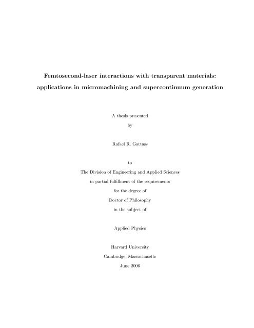
Chapter 2: History of micromachining 17numerical apertures above 1.0, the threshold energy drops below the pulse energy deliveredby a typical femtosecond <strong>laser</strong> oscillator. Oscillator-only micromachining is fundamentallydifferent from micromachining <strong>with</strong> amplified <strong>laser</strong> systems. Because the average outputpower is limited by the pump source, there is a trade-off between the pulse energy and pulserepetition rate of femtosecond <strong>laser</strong>s. The time interval between the pulses emitted by afemtosecond <strong>laser</strong> oscillator is on the order of tens of nanoseconds, which is significantlyshorter than the 1-µs heat diffusion time out of the focal volume. Consequently there is notenough time between successive pulses for the energy deposited by the <strong>laser</strong> pulse to diffuseout of the focal volume. Over time, the energy from successive pulses accumulates in andaround the focal volume, producing damage (see Figure 2.2). The train of oscillator pulsesconstitutes a point source of heat at the focal volume <strong>with</strong>in the bulk of the material. Thelonger the material is exposed to the train of pulses from an oscillator, the higher the temperatureat the focus and the larger the region that is heated. If the temperature exceedsthe materials melting point, structural changes can occur. Schaffer demonstrated meltingand resolidification of material up to a radius of 50 µm [29, 30]. The pulses from an amplifiedfemtosecond <strong>laser</strong> system, on the other hand, typically are separated by milliseconds,which far exceeds the time required for heat to diffuse out of the focal volume. The focalvolume thus returns to room temperature before the next pulse arrives. Consequently, thestructural change caused by an amplified <strong>laser</strong> is confined to the focal volume, regardless ofthe number of pulses that strike the sample.One of the most exciting applications of femtosecond micromachining of <strong>transparent</strong>materials is the fabrication of three-dimensional waveguide structures – critical componentsfor future integrated optical “ chips” . Both femtosecond oscillators and amplifiedsystems have been used to fabricate a number of simple devices, from beam splitters toamplifiers and resonators (Table 2.1). The index of refraction change is roughly the same
Chapter 2: History of micromachining 18SELF-CHANNELINGLONGITUDINALTRANSVERSELOW NAHIGH NAFigure 2.3: Different geometries may be used for micromachining waveguides in the bulkof <strong>transparent</strong> samples. The self-channeling and longitudinal geometries are usually used<strong>with</strong> amplified systems. Oscillator-only micromachining is performed transversely.for both low (amplified) and high (unamplified) repetition-rate waveguide writing, althoughthe gamut of materials used for low repetition rate machining (below 1 MHz, where pulseenergy is not a limitation) is much larger. At low repetition rates, waveguide writing canbe done in several geometries (Figure 2.3). A simple, but limited way to micromachinewaveguides is to let non-linear effects confine the femtosecond beam to a self-channelingfilament. Typically the self-channeling is achieved <strong>with</strong> a lens of long focal length and themicromachining occurs throughout the filament. Waveguide dimensions can be controlledby altering the focusing and input power. Because the resulting waveguide is necessarilystraight, this geometry does not allow the micromachining of devices that include curvesor bends. Another widely used geometry is that of longitudinal irradiation: a long workingdistance objective <strong>with</strong> a fairly low numerical aperture is used to focus the beam inside thesample, which is translated parallel to the beam during irradiation. Because the waveguideis manufactured parallel to the irradiation direction, the diameter is defined by the transversebeam profile, making it possible to achieve fairly large core diameters. This techniquealso allows fabrication of curves and bends, but the working distance of the objective limits
Chapter 2: History of micromachining 19the length of the waveguide. Transverse micromachining puts no limit on the length of thewaveguide, but the cross section of the waveguide typically is elliptical because the structuralmodification is localized to the focal volume. To obtain a more spherical focal volumeand minimize the ellipticity, the beam can be shaped using an astigmatic lens. In the caseof high-repetition rate, oscillator-only machining, the geometry is restricted by the maximumpulse energy available. Usually a high numerical aperture objective (NA≥ 1) mustbe used, which necessitates a transverse writing geometry. The diameter of the waveguideis controlled by the translation speed of the sample: the slower the translation speed, themore pulses strike the same spot. When more pulses strike the same spot, the radius towhich the material is heated above the melting point increases and so does the diameterof the final waveguide structure. Because this diameter is determined by heat diffusion,the cross section of waveguides fabricated this way is very nearly circular. The very highrepetition rate of oscillators permits the fabrication of devices at writing speeds that aretypically 100 – 1000 times higher than those obtained <strong>with</strong> amplified <strong>laser</strong> systems.The writing of internal waveguides makes it possible to wire optical breadboardsand the devices listed in Table 2.1 comprise a basic tool chest of passive and active componentsfor integrated optical circuits. The technique is a major step towards the realizationof optical integrated circuits. Major advantages of optical signal processing over electronicintegration are the ability to connect in three-dimensions and the lack of thermal energy dissipation.However, femtosecond <strong>laser</strong> micromachining is a sequential process – each circuitneeds to be wired separately. Oscillator-only micromachining relieves some of this limitationby making it possible to write at very high speeds. In addition, the past few years have seenthe rapid development of smaller, simpler, cheaper and more powerful femtosecond <strong>laser</strong>oscillators. These developments greatly benefit waveguide writing <strong>with</strong> femtosecond <strong>laser</strong>sby providing greater control of the diameter of waveguides, increasing the speed at which
Chapter 2: History of micromachining 20devices can be made, and greatly broadening the range of materials that can be machined.Overall, waveguide writing <strong>with</strong> femtosecond <strong>laser</strong>s is a promising method for wiring lightin integrated optical devices. It may be just a few years before an integrated optical devicemanufactured by femtosecond <strong>laser</strong> micromachining is used in a commercial application.Device Repetition rate Pulse energy NA GeometryWriting speed(mm/s)Index change( ×10 −3 )Amplifier [31] 0.25 kHz 4 µJ 0.1 longitudinal 0.025Mach-Zehnder [32] 0.25 kHz 1−10 µJ 0.55 longitudinal and transverse 0.0250.200 4Y-coupler [33] 1 kHz 1 µJ 0.16 self channeling 0.020 3-5Amplifier [34] 1 kHz 1 µJ 0.30.6 beam shaped transverse 0.020 2Waveguide [35] 1 kHz 20 µJ 0.007 self channeling 5Waveguide [36] 200 kHz 0.2−4 µJ 0.10−0.25 transverse and longitudinal 0.010 10Mach-Zehnder [37] 4 MHz 20 nJ 0.6 transverse 10 15Waveguide [29] 25 MHz 5 nJ 1.4 transverse 20 0.3Waveguide [38] 80 MHz 7−9 nJ 0.26 longitudinal 0.001−0.100 5Table 2.1: Optical device components manufactured by femtosecond <strong>laser</strong> micromachiningof <strong>transparent</strong> materials together <strong>with</strong> the conditions for fabrication and resulting changein index of refraction. The shaded part of the table shows devices fabricated <strong>with</strong> just a<strong>laser</strong> oscillator.
Chapter 3Micromachining <strong>laser</strong> systemsHistorically tmany <strong>laser</strong> designs have been used for femtosecond micromachining[39], however for oscillator-only micromachining the designs have been rather limited to“home-built” systems [29, 37, 40, 41]. The systems were developed by research laboratorieswho constantly pushed the limit of pulse energies and repetition rates.As a drawback,these <strong>laser</strong>s relied on very experienced maintenance staff (usually the same people whodeveloped them). Recently though, motivated by the growing use of femtosecond <strong>laser</strong>s formicromachining in biological materials [42], the <strong>laser</strong> industry has joined in the productionand developement; and several new designs are being proposed and sold [43, 44].In this chapter we will review the <strong>laser</strong> system used for all the micromachiningexperiments presented in this thesis and place its advantages (and disadvantages) in contextto the new systems.3.1 Extended cavity oscillatorThe single-shot damage intensity threshold is rather invariant <strong>with</strong> respect to thebandgap of the material under irradiation [45].Table 3.1 presents values for the inten-21
Chapter 3: Micromachining <strong>laser</strong> systems 22Bandgap (eV) Damage intensity threshold ( ×10 17 W/m 2 ) # of 800-nm photons3.3 1.3 34.4 2.8 37.5 3.2 510.2 4.5 7Table 3.1: Damage intensity threshold for various materials <strong>with</strong> different bandgaps andthe estimated number of 800-nm photons required to bridge the bandgap [45].sity threshold for materials <strong>with</strong> increasing bandgap. The damage intensity threshold onlyincreases from 1.3 × 10 17 W/m 2 to 4.3 × 10 17 W/m 2 even though the bandgap increasesthreefold (showing that multi-photon absorption is not the dominant mechanism 1 ).So,assuming we can focus to a 1 µm 2 spot size, the energy required to reach this threshold isabout 10 nJ for a 100-fs <strong>laser</strong> pulse. Experimentally, the damage threshold pulse energyis reported as the amount of energy that needs to be delivered at the sample. A typicalmicromachining setup will have many additional elements in the optical path between the<strong>laser</strong> output and the sample. A schematic of our setup is presented in Figure 3.1. Afterpropagating through all the optics in the beam path including a faraday isolator, a prismcompressor, an acousto-optic modulator and a microscope objective, the overall transmissionloss is on the order of 40 %. Therefore, for the delivery of 10 nJ at the sample, the <strong>laser</strong>system must have an output energy of at least 16 nJ. Most commercial <strong>laser</strong> oscillators soldwhen this project started in 2001 were inadequate 2 , providing at most 8 nJ [44].The output power of a <strong>laser</strong> system scales linearly <strong>with</strong> the pump power for powersgreater than the lasing threshold and stabilizes as the gain saturation power is reached [46].Our current <strong>laser</strong> design uses all the power available from our pump <strong>laser</strong> (10 W). The1 An increase in the bandgap of this magnitude would change the multi-photon absorption from thirdorder to seventh order. If multi-photon absorption was the dominant mechanism, the intensity thresholdwould have increase in power accordingly.2 It could be argued that certain optical elements are not essential in a micromachining setup, such as theacousto-optical modulator. The modulator will be required for a series of experiments presented in Chapter5 but introduces less than 3 % loss when disconnected.
Chapter 3: Micromachining <strong>laser</strong> systems 23objectivecompresormodulator<strong>laser</strong>prismpairisolatorFigure 3.1: Schematic diagram of our micromachining setup. The spatial distribution ofthe elements (<strong>laser</strong>, isolator, external prism pair, compressor, acousto-optic modulator andmicroscope objective) mimics the one used in the experiments in Chapter 4 and 5.<strong>laser</strong> pulse energy is further increased by using an extended cavity oscillator design. Byreducing the repetition rate of the <strong>laser</strong> but still maintaining the same average power, thepulse energy is increased. To make the point even more clear, the average power generatedby a pulsed <strong>laser</strong> is related to the repetition rate ν and pulse energy, E pulse byP ave = ν × E pulse (3.1)A schematic of the <strong>laser</strong> used in the micromachining experiments is shown inFigure 3.2. Originally built from a Kapteyn-Murnane Ti:Sapphire kit (Fig. 3.2A ) [47, 48],the <strong>laser</strong> was modified by extending the cavity of the <strong>laser</strong> by 4 meters (Fig. 3.2B) [49,50].The <strong>laser</strong> cavity can be extended under the constraint that the gaussian beam mode remainthe same before and after propagating through the added length to the cavity (q = 1 matrixtransformation) [49, 51, 52]. Extending the cavity by such a large amount (∼ 3.5 times theoriginal cavity) <strong>with</strong>out worrying about imaging the mode could be done by simply movingthe output coupler farther away. This design posses a totally different stability boundarybeing inherently unstable <strong>with</strong> respect to small vibrations of the output coupler mirror [46].
Chapter 3: Micromachining <strong>laser</strong> systems 24(A)M1 M2Coherent Verdi532 nmHighReflector 18 %O. C.(B)25 %O. C.M1M2Coherent Verdi532 nmM6M7M3M5M4Figure 3.2: Schematic diagram of the <strong>laser</strong> system used for micromachining. (A) Theoriginal system based on the Kapteyn-Murnane kit. (B) Extended cavity oscillator. Thecavity has 4 meters added through a telescope (M6-M3-M7-M6-M4). M1,M2: 0.1 m radiusof curvature mirrors, lens: 0.2 m focal length, M3: 2m radius of curvature mirror, M4: 0.5m radius of curvature mirror, M5: saturable absorber. The prism sets used is (A) and (B)are made of fused silica [47,48]. In (B) the distance has been increased to take into accountthe extra dispersion introduced by air [53].In our design, the extension of the cavity is accomplished <strong>with</strong> a telescope composed of atwo meter radius of curvature mirror (M3) that is used both as the input and output lens.In theory, the mode of the <strong>laser</strong> beam is mapped <strong>with</strong>out change of size and divergence toa position four meters away. Implementing this design <strong>with</strong> the parts we had available ledto some additional constraints. Physically it was not possible to use only two mirrors toform a telescope. The limited size of the beam combined <strong>with</strong> the limited space (and thedesire to minimize the astigmatism) led to a telescope design based on four-mirrors. Thefinal design was a compromise between a perfect telescope and these practical constraints.
Chapter 3: Micromachining <strong>laser</strong> systems 25Ideally the selected design would allow for the pulse energy to be increased indefinitelyby scaling (increasing) the pump power accordingly. In practice, this claim isfalse. By increasing the pulse energy traveling <strong>with</strong>in the cavity, the nonlinearity inside theTi:sapphire crystal is enhanced and leads to pulse splitting [54–57]. The energetic pulsesplits into two or more pulses as it propagates through the crystal, distributing the energyof the single pulse between the multiple pulses. Nonlinearly driven pulse-splitting representsa practical limit to the maximum pulse energy.One change implemented to reduce multiple pulse instabilities was to reduce thepower inside the cavity, directly reducing the nonlinearities inside the crystal. We replacedthe 18% output coupler by a 25% output coupler allowing high output pulse energies whilereducing the intracavity power 3 . Similar designs have also changed the lens used to focusthe pump into the crystal, increasing the focal volume excited by the pump and directlyreducing the nonlinearity inside the crystal [40].Another change implemented to reduce multiple pulse instabilities was to use ofa saturable absorber mirror (SAM) [59–61].The structure of the SAM consists of anAlAs/Al 0.15 Ga 0.85 As quarter-wave dielectric stack grown by molecular beam epitaxy and asingle GaAs quantum well [59]. The SAM acts as a mirror (albeit a bit lossy) at low fluences,but has about a one percent reflectivity increase if excited above the saturation fluence ofthe quantum well. Although a 1% change in reflectivity may seem small, the overall effectinside a cavity is to favor pulsed operation instead of continuous wave. Inside a cavity, lasingdepends on a balance between gain (at the active media) and loss. The SAM introduces anintensity dependent loss. If at any point a pulse is formed inside the cavity <strong>with</strong> enoughenergy to saturate the quantum well, the pulse propagates inside the cavity <strong>with</strong> less lossthan any other mode.After several round trips, the larger loss suppresses other modes3 For all <strong>laser</strong> designs there is an optimal output coupler [58]
Chapter 3: Micromachining <strong>laser</strong> systems 26and the pulse remains. Additionally, the SAM provides stability against multiple pulsingby controlling the incident fluence. The fluence incident on the SAM is tuned so that if apulse splits into multiple less energetic pulses, the resulting fluence does not saturate thequantum well. Overall, the multiple pulses incur a higher loss than a single energetic pulse.The efficacy of the saturable absorber mirror to suppress multiple pulsing instabilitiesis directly dependent on the fluence incident on the SAM [59–63]. To achieve thenecessary fluence a curved mirror was introduced on the long arm of the <strong>laser</strong> (M4). Severalcurved mirrors of different radius of curvature were tested (always place at position M4).Best results were obtained <strong>with</strong> a 0.5-m radius of curvature mirror. The use of a curvedmirror introduced a new focus in the cavity and the location of the output coupler had tobe changed(a SAM design to act as output coupler has been developed as well [64]). Thenew output coupler location is on the spatially spectrally dispersed side, and for that reasonanother set of prisms (shown outside the cavity in Fig. 3.1) is needed to remove the spatialchirp before performing any experiment.The initial goal of increasing the pulse energy of the <strong>laser</strong> by extending the cavityled to more changes than just the introduction of a telescope. The concern over multiplepulsing strongly influenced the final design. The new <strong>laser</strong> layout (Fig. 3.2) contained notonly the introduction of a telescope but also a new focus inside the cavity and a new outputcoupling position.Figure 3.3 shows a typical spectrum for our <strong>laser</strong> system. Contrary to the originalKMLabs kit, which produces a nearly gaussian spectrum, the spectrum of our <strong>laser</strong> is full offeatures. The spectrum’s shape indicates that the mode locking mechanism has shifted frompurely Kerr-lens based to a mix between Kerr-lensing and loss modulation at the saturableabsorber mirror.Perhaps the greater indication of the change in the modelocking mechanism is the
Chapter 3: Micromachining <strong>laser</strong> systems 271.0intensity (a.u.)0.50750 800 850wavelength (nm)Figure 3.3: Typical mode-locked <strong>laser</strong> spectrum.reflectivity of the saturable absorber.The shape is likely influenced by themode shape. Laser designs based on Kerr-lensing use a aperture (soft or hard) to favorpulsed operation. In Kerr lens based designs, the mode reduces in size (or divergence) whenmodelocked. The cavity is tuned (by moving some of its mirrors or by closing an aperture)so that the quality factor of the cavity is larger for a <strong>laser</strong> pulse traveling inside the cavitycompared to continuous wave mode. The original KMLabs kit behaved this way <strong>with</strong> themode changing from an asymmetrical oval to a round TEM 00 upon modelocking. Once allchanges were implemented, our <strong>laser</strong> no longer had that feature. The <strong>laser</strong> mode shape isidentical in continuous and pulsed operation.The <strong>laser</strong> pulse has to travel through a significant amount of material prior toreaching the sample (used in the micromachining experiments), accumulating a large amountof dispersion. A prism compressor was built to tune the group velocity dispersion of thepulse and control the pulse width anywhere along the setup. Figure 3.4 shows the autocorrelationtrace taken for two different positions of the external prism compressor. Theautocorrelation trace shown in Fig. 3.4 (A) represents the shortest pulse duration supportedby the <strong>laser</strong>: 55 fs. In Fig. 3.4 (B), we show the autocorrelation trace for the pulse used inmicromachining. The pulse is “pre-chirped” – dispersed such that the shorter wavelengths
Chapter 3: Micromachining <strong>laser</strong> systems 28second harmonic signal (a.u.)1.00.5(A)0–2 –1 0 1 2time delay (ps)second harmonic signal (a.u.)0.25(B)0.200.150.100.050–2 –1 0 1 2time delay (ps)Figure 3.4: Intensity autocorrelation traces for: (a) transform limited pulse and (b) prechirpedpulse. Both signals are shown on the same scale. Minimum pulse width for (a) 55fs and (b) 250 fs.arrive before the longer wavelengths – to take into account all dispersion yet to come furtheralong the beam path. Once pre-chirped the pulsewidth becomes about 250 fs.The optimum pre-chirped pulse width is determined by measuring the damagethreshold of the sample we want to micromachine and minimizing the energy required fordamaging its bulk. Because the value of the damage threshold intensity is constant for anygiven sample, if we can damage the sample <strong>with</strong> less energy, the pulse width reaching thesample (at the focus of the microscope objective) must be shorter. This procedure can berepeated iteratively until the minimum pulse width at the focus is found.Our measurements for the pulse width are not done in situ. The pulse width atthe focus has been measured by other authors [65]. It has been shown that the dispersionintroduced by most elements in a micromachining setup can be removed by pre-chirping [65].Using an external prism compressor, the minimum pulse width is recovered at the focus ofa microscope objective. For this reason, we assume the minimum pulse width at the focusis identical to the minimum pulse width measured at the autocorrelator (55 fs).It is interesting to estimate how much dispersion is induced by all the elementsin the optical path between the <strong>laser</strong> output and the sample. The dispersed pulse width τ
Chapter 3: Micromachining <strong>laser</strong> systems 29after all elements is related to the minimum pulse width τ 0 for a gaussian pulse by [66]( ) 4 ln(2) GV D × L 2τ = τ 0√1 +(3.2)τ 0where the group velocity dispersion 4 (GVD) measures the dispersion in units of [s 2 /m]and L is the distance propagated in a dispersive medium. Using the pre-chirp pulse widthdetermined by the minimum energy damage threshold as a value for τ and knowing theminimum pulse width is 55 fs, we solve Eq. 3.2 for the total group delay dispersion andarrive at GV D ∼ 7500 fs 2 . This value is in agreement <strong>with</strong> the expected dispersion of atransformed limited beam propagating through a microscope objective (1200 fs 2 ) [65] anda TeO 2 acousto-optic modulator (6000 fs 2 )).3.2 Other <strong>laser</strong> systemsOnce all the modifications were implemented, the <strong>laser</strong> parameters became: 25-MHz repetition rate, 55-fs pulse width and 20 nJ pulse energy centered around 790 nm.In 2001, when this <strong>laser</strong> was constructed, it represented one of the few systems (I woulddare say 3) that had tens of nanojoules of pulse energy at megahertz repetition rate andfemtosecond pulse duration. As stated in the introduction, this is no longer true and thereis a growing spread of similar <strong>laser</strong>s.Table 3.2 presents a short summary of similar <strong>laser</strong>s and their main parameters.Long cavity oscillators continue to be developed. For example in 2003, by simply extendingthe <strong>laser</strong> cavity even further <strong>with</strong>out major changes, 150 nJ <strong>laser</strong> pulses at 5.85 MHz weredemonstrated. [40] Although this <strong>laser</strong> represents an engineering feat, it still suffers from aninherent lack of stability <strong>with</strong> respect to multiple pulses. Long-term stability and scalabilityin power are both lacking in this <strong>laser</strong> design.4 A detailed treatment of dispersion will be given in Chapter 7.
Chapter 3: Micromachining <strong>laser</strong> systems 30In 2004, both issues (stability and power scalability) were addressed <strong>with</strong> theintroduction of a new design for <strong>laser</strong> oscillators: chirped-pulse oscillators. [67] The conceptis based on managing the dispersion inside the cavity; the <strong>laser</strong> pulse duration is controlledsuch that the nonlinearity inside the crystal is low enough to avoid multiple pulsing. Thedesign, made possible mainly by innovative chirped mirrors [68,69], allows for output powerscalability by altering the location where the pulse is shortest inside the cavity. The cavityis designed such that the <strong>laser</strong> pulse duration is long enough when inside the crystal tostill allow for Kerr-lensing but small enough so that pulse splitting does not occur. Thesechirped-pulse oscillators, contrary to standard femtosecond oscillators, work <strong>with</strong> an overallpositive dispersion 5 . Higher-order nonlinearities need to be included to explain the theoryfor mode-locking in the chirped-pulse design and are not presented here. [70,71] The chirpedpulseoscillator design has shown as much as 80 nJ at 50 MHz – limited only by the availablepump power – and up to 500 nJ at 2 MHz. [67, 72]From a materials perspective, Ytterbium (Yb) represents an attractive alternativeto Ti:Sapphire as an active medium for femtosecond <strong>laser</strong> sources. The main reasons areits large gain bandwidth (Yb can support down to 20 fs pulses), the availability of cheapersolid state pump sources, large saturation fluence and the ease of incorporating Yb intoglass [73, 74]. Besides standard oscillator designs based on Yb:glass, there are more andmore demonstrations of fiber based <strong>laser</strong>s <strong>with</strong> sub-picosecond time durations [75–78]. Theuse of fibers for <strong>laser</strong>s brings the advantage of excellent mode profile, small footprint andminimal maintenance. Although Yb can support 20 fs, high power fiber based Yb <strong>laser</strong>shave yet to achieve such a pulse width, <strong>with</strong> the record standing at 220-fs <strong>laser</strong> pulses of1800 nJ at 76 MHz [79].The <strong>laser</strong> systems shown in Table 3.2 were selected for their direct application into5 The calculation for total dispersion of the oscillator cavity does not take into account dispersion from nonlinearprocesses, therefore when in stable operation the pulse width has zero total effective dispersion [70,71].
Chapter 3: Micromachining <strong>laser</strong> systems 31Authors Rep. rate (MHz) E (nJ) λ (nm) τ (fs) GeometryKowalevecz [40] 5.85 150 800 43 extended-cavityFernandez [67] 11 220 800 30 chirped-pulse oscillatorNaumov [72] 2− 50 MHz 500−50 800 100 chirped-pulse oscillatorKilli [75] 0.2 400 1045 ? Yb:glassOsellame [76] 0.166 270 1040 300 cavity-dumped Yb:glassGalvanauskas [77] 1 MHz 1000 1045 220 Yb:fiberRoser [79] 73 MHz 1800 1040 220 Yb:fiber amplifierTime-bandwidth Inc. [80] 4.1 25 825 100 cavity-dumped SESAM assistedIMRA Inc. [81] 5 MHz 100 1045 500 Yb:fiber amplifierFemto<strong>laser</strong>s Inc. [43] 11 MHz 80 nJ 800 50 chirped-pulse oscillatorCoherent Inc. [44] 76 MHz 40 nJ 800 160 18W pumped Ti:S oscillatorTable 3.2: Currently avaliable alternative <strong>laser</strong>s used for micromachining. The shaded partof the table shows commercially sold systems.high repetition rate <strong>laser</strong> micromachining. However, their efficacy for micromachining willnot be dictated solely by energy and repetition rate. For every pulsewidth and wavelengththe damage threshold is different. For the systems based on Ti:Sapphire crystals and sub-100 fs pulses, the damage threshold is ≈ 30 nJ at 1.4 NA focusing for fused silica [45, 82].Meanwhile, when using a Yb:glass <strong>laser</strong>, just the fact that the center wavelength of the <strong>laser</strong>is 1045 nm leads to a higher damage threshold energy (≈ 300 nJ at 1.4 NA focusing for fusedsilica [83]) . Therefore, the impact of the <strong>laser</strong> parameters on the damage threshold needs tobe considered carefully when choosing a new <strong>laser</strong> system for micromachining experiments.3.3 OutlookThe <strong>laser</strong> we built in 2001 to perform the micromachining experiments providesabout 20-nJ pulses, centered around 790-nm <strong>with</strong> 55-fs duration at 25-MHz. The <strong>laser</strong> hasbeen sufficient for performing experiments in multiple samples, yet there are some substrates
Chapter 3: Micromachining <strong>laser</strong> systems 32whose damage threshold is outside the range accessible <strong>with</strong> this <strong>laser</strong>.The main problem is poor focusing into high index materials. Microscope objectivesare corrected to focus ideally in either glasses <strong>with</strong> a refractive index of 1.5 or inwater. The larger the numerical aperture of the lens, the larger the aberration induced byfocusing into a material <strong>with</strong> different index than the one which the microscope objective isdesigned. Poor focusing leads to an increase in the spot size and consequently a reductionin the incident intensity. To compensate, more pulse energy is required. Given that thepulse energy of our high repetition rate <strong>laser</strong> is capped at 20 nJ, we remain limited in thesamples we can micromachining.The second problem associated <strong>with</strong> focusing is the focusing depth. High numericalaperture objectives provide a small focal spot but restrict the depth of focus to about 200µm. In general three-dimensional freedom is one of the main advantages of femtosecondmicromachining, and using a high numerical aperture lens severely limits this ability. Lownumerical aperture lenses can be used at the expense of a larger focus spot and the need oflarger pulse energy. Indeed, we have performed experiments <strong>with</strong> low numerical apertureslenses but only in materials <strong>with</strong> low damage thresholds.As previously stated, this <strong>laser</strong> was built <strong>with</strong> a specific goal in mind: high repetitionrate micromachining of <strong>transparent</strong> materials. Recently, however, many applicationsin biological materials have spun from research on femtosecond micromachining. For biologicalapplications it is interesting to image through multiphoton excitation of a dye andselectively disrupt through nonlinear ionization. To accomplish the first goal, imaging, ahigh repetition rate <strong>laser</strong> <strong>with</strong> tunable center wavelength is ideal. For disruption, high pulseenergies are needed. A design similar to the one we currently employ could provide a single<strong>laser</strong> for sue in both applications.The <strong>laser</strong> design we currently use is limited in its application to micromachining.
Chapter 3: Micromachining <strong>laser</strong> systems 33Depending on the project’s future direction, a design based on a chirped-oscillator could beimplemented <strong>with</strong>in three months at the price of a new set of chirped mirrors for the cavity.That being said, this <strong>laser</strong> remains well suited for studying low damage threshold materials.The damage threshold of polymers is an order of magnitude smaller than in most glassesand the previous limitations do not apply.
Chapter 4Waveguides characteristicsIn Chapter 2, we reviewed the history of femtosecond micromachining in <strong>transparent</strong>materials. We learned that by 2001, waveguides had already been manufacturedthrough an oscillator-only technique though characterization of the structures was lacking.This chapter covers the characterization of waveguides manufactured <strong>with</strong> femtosecond <strong>laser</strong>oscillator <strong>with</strong> respect to index profile, supported electro-magnetic modes and transmissionlosses.4.1 Refractive index measurementsThe fundamental characteristic of any waveguide is its spatial refractive indexprofile. [84] All other waveguide characteristics can be calculated from the index of refractionprofile including transverse modes, bending losses, effective NA, etc. The process inducinga refractive index modification through irradiation <strong>with</strong> femtosecond <strong>laser</strong> pulses is stillunder question, providing no guidance for modeling the induced refractive index profile.Up to 2001, information on the refractive index was restricted to a magnitudeestimate of the index change, not accounting for any spatial variation.Estimates from34
Chapter 4: Waveguides characteristics 35divergence measurements of the output beam along <strong>with</strong> beam propagation modeling (basedon the output’s beam divergence) put the refractive index contrast in the range of 10 −3 -−10 −5 [29,33,38,41,83,85–87]. Although this range matches well <strong>with</strong> the index contrast inoptical fibers, measuring this small contrast presents significant technical challenges. Theproblem is compounded by two factors: size of the features and location. Contrary to thecase of optical fibers where the index change has about 100 µm dimension and is easilyaccessible at the front face of the fiber, the index contrast induced through femtosecondmicromachining is localized <strong>with</strong>in the bulk of the sample (usually about 100 µm inside)and has a transverse dimensions on the order of 10 µm. Therefore, the method used formeasuring the index must be able to provide sub-micrometer spatial resolution to resolvesmaller features <strong>with</strong>in a 10 µm 2 area, measure a structure that is embedded inside anotherAND be sensitive to index changes on the order of 10 −5 .In summary, the requirements for measuring the index profile of femtosecond inducedwaveguides are• sub-micrometer spatial resolution• sensitivity to index of refraction variations as low as 10 −5• ability to measure index of embedded structuresThere have been several proposals in the literature for measuring the refractive index inthese structures. The techniques currently used are presented in Table 4.1.Near-field scanning optical microscopy (NSOM) has been used for characterizationof the index of refraction in femtosecond induced structures [88, 97, 98]. In a NSOM setup,a tapered fiber tip is scanned across the end facet of the waveguide (which we assume isexposed) while being kept at a fixed, small distance (usually on the order of 10-20 nm).The index of refraction is determined indirectly either by measuring the reflected light from
Chapter 4: Waveguides characteristics 36Technique Spatial resolution Sensitivity DisadvantagesModeling from transmission [87] none 10 −4 not a direct measurementNear-field optical microscopy [88] nanometer 10 −4 very hard to setupDensity change [89, 90] nanometer relative limited applicationEllipsometry [36] micrometer 10 −3 limited sensitivityDigital holography interferometry [41] micrometer excellent thin sample requiredPhase contrast interferometry [91–93] micrometer medium expensive softwareRefractive near-field [94–96] sub-micrometer excellent hard to setup, expensive machineTable 4.1: Various techniques used to measure the refractive index profile of femtosecond<strong>laser</strong> micromachined waveguides.the end face of the waveguide that is coupled back into the fiber taper or by exciting awaveguide mode and measuring the evanescent field at its output. The dimension of thefiber taper’s tip sets the spatial resolution for both types of measurement, <strong>with</strong> the tipdimensions being generally below 100 nm. A tapered fiber is scanned across the end face ofthe structure and the index of refraction is calculated for each position. The tapered fiber ismounted on an atomic force microscope (AFM), giving the technique nanometer resolution.Depending on the detecting scheme, this technique can be sensitive to index variations aslow as 10 −4 . Its main disadvantage is the need of an AFM setup.An AFM is also used in another technique for measuring index profiles, whichinvolves hydrofluoric acid etching [89, 90].It has been shown that the etching rate ofhydrofluoric acid is related to the density of the silica structures. Because density changesresult in index of refraction changes. So, for materials whose index change originate fromdensification, hydrofluoric acid is used to etch the structures and the index is indirectlyprofiled <strong>with</strong> an AFM [89,90]. Although this technique allows for nanometer resolution, itsmain drawback is the indirect way of measuring the index. There are several other factorsthat may influence the index of refraction change, making this technique questionable for
Chapter 4: Waveguides characteristics 37other systems beyond Ge-doped fused silica [89].A more practical approach to measuring the index profiles comes from interferometrictechniques. There have been two main interferometric techniques used for measuringthe index of femtosecond <strong>laser</strong> induced waveguides: phase-contrast and holography. Phasecontrastmicroscopy measures the phase-shift of light transmitted through the sample atdifferent phase shifts and numerically deconvolves the index of the structure from the opticalpath length [91–93]. The holography method is similar to phase-contrast, except only a thinslice of the sample is used. A hologram is formed from the interference of the beam throughthe sample and a reference beam. The first hologram is compared <strong>with</strong> the hologram generated<strong>with</strong> only the substrate and the index profile is recovered from the optical path length.The spatial resolution is limited by the pixel size of the CCD and the magnification used,and is usually on sub-micrometer scale [41].We have used another technique to measure the index of refraction of our structures:refractive near-field profilometry [94]. The technique will be discussed in detail inthe next section.Refractive near field techniqueRefractive near-field profiling (RNF) is one of the most established techniques formeasuring the refractive index of embedded photonic structures [94, 95, 99].The indexprofile is obtained by measuring the signal associated <strong>with</strong> the deflected beams at theinterface of the waveguide.The strength of this method is its simplicity, the minimalsample preparation and the spatial resolution. The index contrast sensitivity is dependenton the detectors sensitivity and the calibration from two reference blocks. The closer theblocks are to the index range the better the sensitivity.Figure 4.1 shows a schematic of the RNF setup. A collimated <strong>laser</strong> beam incident
Chapter 4: Waveguides characteristics 38on a microscope objective is partially blocked and focused into the sample’s surface. Partof the beam is coupled into the waveguide, and the rest propagates out as a hollow conetowards the detector. The hollow cone is composed of light that coupled into the waveguideand left as leaky modes and a part <strong>with</strong> light purely refracted at the surface. The leakymodes remain on the inside of the hollow cone and are blocked <strong>with</strong> an aperture before thedetector. If we assume small index of refraction variations along the waveguide, the lightpropagates maintaining the transverse component of the wavevector constant. Because thetransverse wavevector remains constant, the incident angle of light is related to the outputangle through [94, 95]n l sin θ in = n(x, y) sin θ W (4.1)at the input face, andn out sin(90 − θ out ) = n(x, y) sin(90 − θ W ) (4.2)at the output face, <strong>with</strong> θ in , θ W , θ out defined in Figure 4.1a.Solving for the input andoutput anglen(x, y) 2 = n 2 in sin 2 θ in + n 2 out cos 2 θ out (4.3)Because we only want refracted light, the beam block is placed at the detector toblock all rays that have [96]θ out ≥ arccos 2n2 min − n2 max(4.4)n in√where we used fact that the waveguides numerical aperture is set by n 2 max − n 2 min . Thedetected signal intensity depends on Eq. (4.3), any index change will change the deflection
Chapter 4: Waveguides characteristics 39(a)(b)detectorθ minreferenceblock 2θ outθ Wn 2n 1sectorialstopreferenceblock 1leaky modeblockhost substratewaveguidediopter3Dpositionstagehigh NAlens<strong>laser</strong> beamθ inFigure 4.1: (a) Incident beam deflection at sample for refractive near-field setup. Angledefinitions used in Eq. (4.3). (b)Schematic of a refractive near-field profilometer. Replicatedfrom Exfo’s OWA-9500 catalog.of light at the input face and hence the signal at the detector. Two (or more) index referenceblocks are used to calibrate the detector response, setting the high and low range for thesample’s refractive index. With the detector calibrated, the waveguide is placed on a threedimensionaltranslation stage and scanned <strong>with</strong> sub-micrometer resolution to get the fullindex profile.4.2 Refractive index profilesThrough a collaboration <strong>with</strong> Sagitta Inc., we have been able to use a commercialrefractive near-field profilometer, EXFO’s OWA-9500. The OWA-9500 uses 656-nm lightfrom a <strong>laser</strong> diode and a 1.4 numerical aperture lens, resulting in 0.5 µm spatial resolution.For every waveguide, the sample was cleaved and polished to expose the end face of the
Chapter 4: Waveguides characteristics 40Figure 4.2: Sample output from the commercial refractive near-field profilometer for awaveguide manufactured <strong>with</strong> 20 mm/s translation speed.waveguide. We collect a two dimensional map of the index profile along the end face ofthe waveguide.Figure 4.2 shows a typical output from the OWA-9500 for a waveguidemicromachined at 20 mm/s translation speed.We fabricated waveguides <strong>with</strong> a Ti:sapphire <strong>laser</strong> oscillator described in Chapter3. The <strong>laser</strong> has a central wavelength of 790 nm, a repetition rate of 25 MHz, an on-targetpulse energy of 7 nJ, and a pulse duration of about 60 fs. The waveguides were fabricatedin 75 x 25 x 1.0 mm 3 silicate glass slides (Corning 0215). The <strong>laser</strong> pulses are focused insidethe sample by a 1.4-NA oil-immersion microscope objective, and the slide is translatedperpendicularly to the incident direction of the <strong>laser</strong> beam (transverse geometry shown inFigure 2.3). The waveguides were written along the length of the slide <strong>with</strong> writing speedsranging from 1 to 20 mm/s. To guarantee no interaction between waveguides, we spacedthe waveguides at least 100 µm apart.Figure 4.3 shows cutouts of the two-dimensional index of refraction maps alongtwo perpendicular directions (as exemplified in Fig.4.2) for samples micromachined at
Chapter 4: Waveguides characteristics 41translation speeds ranging from 2.5 mm/s to 20 mm/s.The magnitude of the index ofrefraction change is shown in the vertical axis ( ×10 −3 ), confirming the claim that theindex change induced between the core and the cladding is on the same order as thoseof a standard optical fiber. For all speeds, narrow shoulders of index increase are presentbut their magnitude decreases <strong>with</strong> increasing translation speed. Additionally, from Figure4.3 (a) and (e), we see that the center portion of the profile shows a relative increase inmagnitude up to 1.5 × 10 −3 as the speed of manufacture is increased.The index profiles allow a clear determination of the size of the generated structures.In the case of complex index of refraction profiles such as the one in Fig. 4.3, thereis no clear method for identifying the core of the waveguide. We can, however, commenton the overall dimension; it decreases as the speed of writing the waveguides increases from11.2 µm at 2.5 mm/s to 8.5 µm at 20 mm/s.4.2.1 Near field modeWe measured the near-field modes for the waveguides whose index of refractiveprofile is presented in Figure 4.3. 1550-nm light was coupled into the waveguides and thenear field was imaged <strong>with</strong> an infrared camera. Figure 4.4 shows the lowest order modefor the waveguides manufactured at 5, 10 and 20 mm/s when excited by a 1550-nm <strong>laser</strong>.Various modes could be excited for the 5- and 10-mm/s manufactured waveguides but whena translation speed of 20 mm/s was used, only a single mode was seen. Figure 4.4(a)-(b)indicate that the waveguides manufactured at 5 and 10 mm/s are multimode.Higherorder modes could be excited by tuning the input coupling conditions.Meanwhile, thewaveguides manufactured at 20 mm/s (Fig. 4.4(c)) are single mode, showing a nice TEM 00mode independent of the coupling condition.
Chapter 4: Waveguides characteristics 426(a)index change (10 -3 )30–3–66(b)index change (10 -3 )30–3–66(c)index change (10 -3 )30–3–66(d)index change (10 -3 )30–3–66(e)index change (10 -3 )30–3–6–20 –10 0 10 20–20 –10 0 10 20distance from center (µm)distance from center (µm)Figure 4.3: Refractive index profiles for waveguides manufactured at different translation’sspeeds. (a) 2.5 mm/s, (b) 5.0 mm/s, (c) 7.5 mm/s, (d) 10 mm/s and (e) 20 mm/s. Leftand right diagrams show two orthogonal directions from the two-dimensional profile.4.2.2 Discussion of index of refraction profilesIn measuring the index of refraction profiles, we observe that not only the size ofthe waveguides but also the index is affected by the number of pulses irradiating the sample.
Chapter 4: Waveguides characteristics 43abcFigure 4.4: 1550-nm near-field mode profiles for waveguides manufactured at (a) 5 mm/s,(b) 10 mm/s and (c) 20 mm/s.We estimate the effective number of shots reaching the focal volume for every translationspeed by assuming the focal spot has 1 µm transverse dimension. The number of pulsesirradiating the focal spot as the sample is translated is related to the repetition rate andthe translation speed by# of pulses = (time to travel 1 µm) × (repetition rate)=()1 µm× repetition rate.translation speedGiven that the <strong>laser</strong> outputs pulses at 25 MHz repetition rate and assuming a 1µm distance, the number of irradiated pulses for the translation speeds in Figure 4.3 areshown in Table 4.2.The observed decrease in the feature size <strong>with</strong> increasing number of pulses (from11.2 to 8.5 µm as the speed changes from 2.5 to 20 mm/s) can now be put in perspective. In2001, the dependence of the structure size on the number of pulses irradiating a fixed spotfor a 25 MHz pulse train from a femtosecond <strong>laser</strong> oscillator was investigated [29]. It wasobserved that the radius of the structures changes from about 2 to 10 µm as the numberof irradiating pulses increases from 10 2 to 10 5 . [30]. Therefore, it is reasonable that thedimensions of the waveguides we fabricated in our experiments do not change significantly
Chapter 4: Waveguides characteristics 44Speed (mm/s)Number of pulses20 125010 25007.5 33335.0 50002.5 7500Table 4.2: Estimates for the number of irradiated pulses assuming a focal spot of 1 µmdiameter for various translation speeds.in size over a one order of magnitude increase in number of irradiates pulses.Up to this point, no comment has been made on the source of the induced indexprofile. The refractive near-field measurement does not provide any information <strong>with</strong> respectto the source of the index. There are several processes that can lead to an increase in therefractive index of a material• density change• stress and strain• color center formation• phase transformation• change of fictive temperatureIt has been proposed that the positive index structure is formed by temperingof the glass matrix [29, 30]. The <strong>laser</strong> pulse train deposits energy at the focus, heating itabove the melting temperature. The heat diffuses out and melts a larger region around thefocus. Once the heat source is removed (i.e. the <strong>laser</strong> is removed), the material cools down.Cooling, however, occurs in the opposite direction from heating starting at the outsidefirst.The outside volume is rapidly quenched, freezing the positions of the atoms in a
Chapter 4: Waveguides characteristics 45high temperature structure. Because most glasses have a lower density structure at highertemperatures, the outside edge is frozen at a lower density. Once the central core starts tocool, it is already surrounded by regions of lower density. Having no space to expand, adenser center core is formed [30].Our observations for the index profile dependence on the number of pulses are indisagreement <strong>with</strong> this model. If true, then the center part should always have a higherindex. We observe the opposite: the index structure is higher at the edges. If densificationwere indeed the only source for an index change, then our measurements would indicatethat the outside edges of the waveguide are denser, not sparser.The increase in the index of the waveguide’s outside has been observed in micromachiningat lower repetition rates and is believed to come from strain on the glassnetwork. The contribution from strain to the index was observed through TEM studies ofquartz [100] and also through polarization microscopy of fused silica [101, 102]. In the caseof quartz, changes to the crystalline network is monitored by diffraction. But for an amorphoussystem like fused silica, it is harder to connect to the atomic morphological changesand so another probe is needed to monitor strain/stress fields. Polarization transmissionmicroscopy of fused silica shows a large birefringence along the edge of a femtosecond <strong>laser</strong>altered spot [101]. However, the estimated contribution from stress alone would amount toonly a 10 −5 index of refraction change, and for the cases of high pulse energy (> 1µJ) eventhough the guided mode is symmetric, the stress field is no longer symmetric [102].The contribution of color centers to femtosecond <strong>laser</strong> induced index change throughKramers-Kronig relations has been dismissed for most cases. [27,30,101] The density of colorcenters required for an index change of 10 −4 would have to be on the order of 10 15 per cm 3in fused silica [101] - an extraordinarily large value. In fused silica, the most common defectsare an Si-E’ defect (resulting from a poorly formed Si-Si bond) and non-bridging oxygen
Chapter 4: Waveguides characteristics 46hole centers. Both defects possess unpaired electrons, having an electron spin resonance(ESR) trace. For the cases where color centers have been observed, annealing did not alterthe refractive index change [33,36,86]. However, annealing close to the melting temperaturedoes remove the defects (as confirmed by ESR), ruling out color centers as possible sourcesfor the refractive index change.Phase transformations could also lead to large index changes, however most systemsstudied by femtosecond micromachining are glass based. Amorphous to crystallinetransitions, although possible, are very unlikely for a drastic process like femtosecond micromachining.Phase transformations from amorphous to another amorphous glass network,on the other hand, are very likely. The various networks supported by amorphous glassesare described by the concept of fictive temperature. [103, 104] Glassy systems are formedby controlled cooling of a melt, <strong>with</strong> their properties depend on the rate of cooling. Althoughthe final temperature is always the same, room temperature, the structure of a glasscan be modeled as a melted network which remains ”frozen” at room temperature. Thefictive temperature is defined by the temperature for which the melted glass would be tohave the structure of the ”frozen” room temperature state. The same material can havemultiple structures at room temperature, each one mimicking the melted glass at differenttemperatures, that is, having different bonding arrangements, density, index, etc. Becausestructures defined by different fictive temperatures can have different physical properties,the concept of fictive temperature represents a combination density and strain contributionsto the refractive index.The fact that Raman measurements point to local density changes [101, 105, 106]while TEM and polarization microscopy support stress contributions makes fictive temperaturean even more attractive quantity to describe the index change. Our results for thespatial index of refraction profile indicate that it is more likely that the structure formed
Chapter 4: Waveguides characteristics 47does not have a spatial homogenous fictive temperature. This is consistent <strong>with</strong> the claimthat the cooling rates for the different regions around the focus are different. Ideally, anexperiment that monitors the temperature as a function of time as the material is micromachined<strong>with</strong> sub-micrometer resolution would be required to build a complete picture.4.3 Optical transmission loss measurementsAlthough many questions remain about the details of the mechanism for the indexchange, numerous studies have investigated waveguide fabrication inside <strong>transparent</strong>materials such as silicate glasses. [29,33,36–38,85,107–109] Indeed, simple photonic devicessuch as waveguide couplers, beam shapers, amplifiers, interferometers and resonators havealready been demonstrated. [29,32–34,37,38,110,111] However, one of the most importantcharacteristics for practical applications of these waveguides, their optical loss, has receivedlittle attention. [41, 83, 112] In this section, we report the results of transmission loss measurementsof both straight and curved waveguides written in silicate glass using femtosecond<strong>laser</strong> pulses. We also determine the effective numerical aperture (NA) and scattering lossof these waveguides.4.3.1 Transmission lossA schematic diagram of the loss measurement setup is shown in Figure 4.5. Acontinuous wave <strong>laser</strong> beam from a linearly polarized single-mode He-Ne <strong>laser</strong> (633-nmwavelength) or 1.55-µm diode <strong>laser</strong> is expanded by a 10x telescope T. Iris I1 is used tocontrol the beam diameter and hence the NA of the beam incident on the waveguide.A beam-splitter directs half the beam onto photo-detector D1 used to monitor the inputenergy. The <strong>laser</strong> beam is focused onto the input surface of the waveguide using a 0.25-NA(10x) microscope objective, and a CCD camera is used to monitor the input coupling. The
Chapter 4: Waveguides characteristics 48D1PTI1I2<strong>laser</strong>sampleD2CCDlampFigure 4.5: Loss measurement setup for optical waveguides written in glass by femtosecond<strong>laser</strong> pulses. P = polarizer; T = telescope, I1,2 = iris, D1,2 = detector; CCD = chargedcoupleddevice camera.output of the waveguide is collected by an objective and measured by detector D2. Outputiris I2 prevents scattered transmitted light from reaching the detector. Incoherent light froma lamp illuminates the input surface of the waveguide to ensure that the input <strong>laser</strong> beamis focused exactly on the waveguide. The CCD image allows us to optimize the coupling oflight into the waveguide before each measurement. Detector D1 measures the input powerof the waveguide after calibrating the transfer efficiency for the beam splitter, the inputobjective, and the Fresnel reflection on the input surface. Detector D2 measures the outputpower through the waveguide after calibrating the transfer efficiency of the output objective,beam splitter, and the Fresnel reflection on the output surface of the waveguide.To determine the transmission losses we cut the glass slides in half, polished theend faces, and then measured the intensity of the transmitted signal through the shortenedwaveguide. The transmission loss is determined from the ratio of the transmission of theoriginal waveguide to that of the shortened waveguide. Figure 4.6 shows the transmissionloss of waveguides fabricated at various translation speeds measured <strong>with</strong> an incident NAof 0.03. Each datapoint is the average of about twenty measurements. In the visible at a
Chapter 4: Waveguides characteristics 490.5average loss (dB/mm)0.40.30.20.1633 nm1.55 µm00 5 10 15 20writing speed (mm/s)25Figure 4.6: Translation speed dependence of the optical loss at 633 nm (triangles) and 1.55µm (circles). Error bars show variance among 10 waveguides written at the same speed.wavelength of 633 nm, the average loss is about 0.3 dB/mm and the minimum loss is 0.16dB/mm. In the infrared the loss is much lower; at a wavelength of 1.55 µm the averageloss is 0.05 dB/mm and the minimum loss 0.029 dB/mm. The higher loss at 633 nm canbe attributed to the greater sensitivity of shorter wavelengths to inhomogenities of thewaveguide, such as sidewall roughness. The optical loss of the waveguides is acceptable forapplications in integrated optical circuits which require wave guiding over relatively shortlengths (e.g., several millimeters).Because the waveguides result from the melting and resolidification of the glassaround a spherical focus they have a circular cross-section and should be polarizationinsensitive.We measured the polarization-dependence of the transmission by using a linearpolarizer and a half-wave plate before the input objective and measuring the output of
Chapter 4: Waveguides characteristics 50100transmissivity (%)902%800 15 30 45angle (degree)Figure 4.7: Laser beam input polarization dependence of optical loss.the waveguide. Figure 4.7 shows the variation of the transmitted signal for different inputpolarizations. The maximum loss difference for two different linear polarizations in waveguidesfabricated at 5 mm/s is only 0.003 dB/mm at 633 nm, confirming the polarizationindependenceof the waveguides.4.3.2 Numerical aperture from divergence measurementsIn section 4.1 we presented the measured values the refractive index profile ofthe waveguides from refractive index near-field profilometry. Using the index profile, wecan calculate the numerical aperture of the waveguide. [84] To cross-check the NA of thewaveguides, we measured the dependence of the transmission loss on the NA of the input
Chapter 4: Waveguides characteristics 510.250.40633 nm1.55 µmloss (dB/mm)0.20loss (dB/mm)0.200.150 0.05 0.10 0.15input numerical aperture00 0.05 0.10 0.15input numerical apertureFigure 4.8: Dependence of the coupling loss on numerical aperture of the input beam at633 nm (top) and 1.55 µm (bottom).beam by changing the aperture of iris I1. By underfilling the microscope objective used tocouple the light into the waveguide, the effective NA is reduced. If the NA of the inputbeam is larger than the NA of the waveguide, less light is coupled into the waveguide andso the loss should increase. Figure 4.8 shows the NA dependence for waveguides fabricatedat a speed of 20 mm/s. The loss increases once the NA of the input beam exceeds 0.04(at 1.55 µm) and 0.065 (at 633 nm). The NAs of waveguides fabricated <strong>with</strong> lower speedsrange from about 0.055 to 0.075 (at 633 nm) and 0.03 to 0.06 (at 1.55 µm).From the NA measurement, we can determine the modes that the waveguides cansupport from the normalized waveguide parameter [3]V = πd(NA)λ 0, (4.5)where d is the diameter of the waveguide, and λ 0 is the vacuum wavelength. For a waveguidefabricated <strong>with</strong> a writing speed of 20 mm/s, the diameter measured from optical microscopyis 10 µm and the NA at 633 nm is 0.065, which gives V = 3.23 according to Eq. 4.5.The single mode condition is V < 2.405, indicating that the waveguide is multimode atthis wavelength.Imaging the near-field pattern onto a CCD shows a LP 11 mode (Fig.
Chapter 4: Waveguides characteristics 52abFigure 4.9: Near-field output of a waveguide fabricated at 20 mm/s. (a) LP 11 mode at633-nm wavelength and (b) LP 01 mode at 1.55-µm wavelength.4.9a), confirming multimode operation. At 1.55-µm wavelength, the normalized waveguideparameter V is 1.32, and the near-field pattern is single mode (Fig. 4.9b).The measured NA allows us to estimate the index change (∆n) of the waveguides.Assuming a square index profile, NA = √ n 2 1 − n2 2 , where n 1 is the index of the waveguide,and n 2 is the index of the substrate glass. [3] For Corning 0215, n 2 = 1.52. For a waveguide ofNA = 0.065, the index change ∆n is about 1.4 x 10 −3 , which is of the same order as thosepreviously reported in similar materials and in agreement <strong>with</strong> our RNF measurements.[33, 37]4.3.3 Bending lossWe also measured the bending loss of curved waveguides that were fabricated bymounting the glass substrate on a rotating stage. The resulting waveguides were obtainedat translation speeds ranging from 3.5 – 7.5 mm/s; the angle subtended by the curvedwaveguides is larger than 45 ◦ . Figure 4.10a shows an optical microscope image of somesample curved waveguides.The loss measurement setup was slightly modified to fit a
Chapter 4: Waveguides characteristics 53aboutput200 µmsampleinputFigure 4.10: (a) Top view of microscope image of a typical curved waveguides, (b) Lightcoupling setup for measuring losses in curved waveguides. The far field output is clearlyvisible at the beam block.curved sample. In Figure 4.10c light coupled from one side of the waveguide curves around,is collected by the microscope objective and propagates into a beam block. While in thestraight waveguides we used the cut back method to measure the losses, the bending loss wasdetermined simply by making waveguides <strong>with</strong> different radii at the same radius of curvatureand measuring their transmission. Because the waveguides have the same curvature, anyincrease in loss comes from the extra propagation along the waveguide.Figure 4.11 shows the bending losses at 633 nm for waveguides <strong>with</strong> differentbending radii. For bending radii larger than 40 mm, the loss is independent of the radiusshowing that at those radii, the loss caused by the bending is negligible. The bending lossincreases rapidly, however, as the bending radius is decreased below 36 mm.4.3.4 Scattering lossTo establish the source of the losses, we measured the scattering loss throughof the waveguides by replacing the detector in the setup shown in Fig. 4.5 <strong>with</strong> a 60mm-diameter integrating sphere, as illustrated in Fig. 4.12. To maximize the coupling
Chapter 4: Waveguides characteristics 5430transmission loss (dB/cm)201000 20 40 60bending radius (mm)Figure 4.11: Bending losses of waveguides <strong>with</strong> different bending radii for an input wavelengthof 633 nm.of light into the waveguide we fixed the NA of the input beam at 0.03. Because of thelow NA of the input beam and high index difference between the polished glass substrateand the air, the substrate acts as a slab waveguide for any light that is scattered from theembedded waveguide. Nearly all the scattered light therefore exits from the far end of thesubstrate slide. With the observing window covered <strong>with</strong> scattering material, we comparedthe detector signal when 633-nm light is coupled into a waveguide to the signal when light ismoved off the waveguide. The ratio of these values gives an upper bound for the additionalloss caused by absorption in the waveguide (on top of the glass matrix absorption). Forstraight waveguides fabricated at writing speeds of 20 mm/s, 10 mm/s and 5 mm/s theseratios are 95%, 96% and 91%, respectively. The transmission losses of these waveguides
Chapter 4: Waveguides characteristics 55detectorprobebeamwaveguidewindowintegratingsphereFigure 4.12: Scattering loss setup. The observation window was covered <strong>with</strong> a scatteringdisk in order to collect all the light coupled into the waveguide.must therefore mainly be due to scattering. Although the waveguides look smooth underoptical microscopy (Figure 4.13), this scattering may arise from sub-micrometer roughnessof the sidewalls caused by vibration during translation of the sample.4.3.5 ConclusionIn conclusion, we determined the losses of straight and curved femtosecond <strong>laser</strong>micromachinedwaveguides in silicate glass slides. The average loss of straight waveguides isabout 0.3 dB/mm at a wavelength of 633 nm and 0.05 dB/mm at 1.55 µm. The polarizationdependenceof the loss is minimal and the bending loss at 633 nm wavelength is negligiblefor bending radii larger than 36 mm. The average NA of straight waveguides is about 0.065at 633 nm and 0.045 at 1.55 µm, corresponding to an index change on the order of 1.4x 10 −3 .Our results also show that in straight waveguides, more than 90% of the totalloss is due to scattering. Optimizing fabrication conditions, especially the stability of thetranslation stage, may further improve optical properties of these waveguides.
Chapter 4: Waveguides characteristics 5650 µmFigure 4.13: Top view microscope image of a typical waveguide.4.3.6 Limitations and outlookThere is still a lot to be done before femtosecond micromachining establishes itself aserious contender for photonic device fabrication. We showed that the losses for these devicesare <strong>with</strong>in an acceptable range for inter- and intra-device signal communications.Theoverall dimensions of the waveguides manufactured <strong>with</strong> high-repetition rate femtosecond<strong>laser</strong>s are of the same order as single mode optical fibers, simplifying a final connectionto optical devices.But the minimum bending radii is still quite large of an “on-chip”application.Other engineering problems still haunt the move of micromachining to industrialenviroments: stability of the <strong>laser</strong> system, edge effects, utilization of sample depth.In
Chapter 4: Waveguides characteristics 57Chapter 3 we discussed alternative for the <strong>laser</strong> system. The are still problems <strong>with</strong> micromachiningthe edges of substrates and utilizing the whole depth of the sample, all addressable<strong>with</strong> more sophisticated focusing optics. Very few applications have been demonstratedthat utilize the three-dimensionality allowed by femtosecond micromachining.The work described in this Chapter addresses one of the claimed drawbacks ofthis technology: the serial nature of device fabrication. The use of a high repetition rate<strong>laser</strong> increases fabrication’s speed by three order of magnitude <strong>with</strong> respect to standardamplifiers, placing the fabrication time of an 1 cm by 1 cm at 1 hour, an acceptable time.From an engineering point, more work on different materials as well as demonstratingmore devices is something we should expect to see over the next decade. <strong>Femtosecond</strong>provides a way to fabricate multiple components in different substrates <strong>with</strong> the interconnectionsdirectly aligned. Even <strong>with</strong> air gaps between pieces, an optically connected waveguidecan be fabricated. The capability to fabricate alignment free optical is another of the mainfeatures provided by femtosecond <strong>laser</strong> micromachining.From a physics research side, a better understanding of the mechanism for indexformation is needed. This would allow the improvement over the total index induced andmost likely reduce the minimum bending radii as the interconnects. But the main questionthat still needs to be answered from a physics point, is how hot does it actually get atthe focus. The variable repetition rate research covered indirectly the left over heat, butit would be interesting to directly measure the maximum temperature the sample reach.And, perhaps in the future, control the temperature to the point of generating micrometersize ovens.
Chapter 5Micromachining <strong>laser</strong> repetitionrate dependence<strong>Femtosecond</strong> micromachining permits the fabrication of waveguides in three-dimensionsinside a material <strong>with</strong>out damaging its surface [27]. A long list of waveguide-based photonicdevices have already been demonstrated including waveguide couplers, beam shapers,amplifiers, interferometers and resonators [29, 31, 34, 37, 38, 82, 110, 111, 113–115]. In 2001,high-speed writing of round waveguides was achieved through oscillator-only micromachining,reducing manufacturing times by three orders of magnitude [29].Oscillator-only micromachining is fundamentally different from micromachining<strong>with</strong> an amplified <strong>laser</strong> system.The pulses from an amplified femtosecond <strong>laser</strong> systemtypically are separated by milliseconds, which far exceeds the 1-µs time required for heatto diffuse out of the focal volume for a typical glass. The focal volume thus returns to roomtemperature before the next pulse arrives (see Figure 5.1a). Consequently, the structuralchange caused by an amplified <strong>laser</strong> is confined to the focal volume, regardless of the numberof pulses that strike the sample. The time interval between the pulses emitted by a fem-58
Chapter 5: Micromachining <strong>laser</strong> repetition rate dependence 59tosecond <strong>laser</strong> oscillator, on the other hand, is on the order of tens of nanoseconds, whichis significantly shorter than the time required for heat to diffuse out of the focal volume(see Figure 5.1b). Over time, the energy from successive pulses accumulates in and aroundthe focal volume, producing structural changes. The train of oscillator pulses constitutes apoint source of heat at the focal volume <strong>with</strong>in the bulk of the material. The longer thematerial is exposed to the train of pulses from an oscillator, the higher the temperature atthe focus and the larger the region that is heated. If the temperature exceeds the materialsmelting point, structural changes can occur.Melting and resolidification of material upto a radius of 50 µm from a 1 µm focal spot has been demonstrated [29, 30], showing thatmicromachined features are controllable by simply varying the number of irradiating pulses.The <strong>laser</strong> repetition rate also has an influence on maximum feature size [116]. Forexample, <strong>with</strong> 10 7 pulses at 0.2 MHz an 8-µm diameter feature is achieved, whereas <strong>with</strong>10 3 pulses at 1 MHz a feature <strong>with</strong> about 18-µm diameter is formed [116]. Hence, a 10 4increase in the number of pulses cannot account for the 1/5 decrease in repetition raterequired for achieving large diameter features, showing that a small deviation in the <strong>laser</strong>repetition rate from the heat diffusion rate has a drastic effect on feature size.Past work focused on the relationship between single pulse repetition rate andfeature size and established the threshold repetition rate for heat accumulation in the focalvolume. In this letter, we present data on the heat accumulation caused by bursts of pulsesfrom a <strong>laser</strong> oscillator at different burst repetition rates. Given the short time interval betweenthe oscillator pulses, we expect a burst of N pulses <strong>with</strong> energy E per pulse to depositthe same amount of thermal energy as a single pulse of energy NE. However, the energy ina burst of pulses is not delivered in the same manner as a single more energetic pulse. Thenumber of pulses in each burst has a pronounced effect on the minimum repetition rate forwhich energy accumulates.
Chapter 5: Micromachining <strong>laser</strong> repetition rate dependence 60ELOW REPETITION RATE1 µs1 mstEHIGH REPETITION RATE40 ns1 µsFigure 5.1: At low repetition rate, the energy deposited by each <strong>laser</strong> pulse diffuses out ofthe focal volume before the next pulse arrives. At high repetition rate, energy accumulatesin the focal volume making it possible to achieve very high temperatures around the focalvolume <strong>with</strong> pulse energies of just a few nanojoules. Yellow: <strong>laser</strong> pulses; red: depositedenergy.tThroughout this chapter we will call the rate at which the bursts of pulses repeatthe ‘repetition rate’ and the intrinsic rate of the <strong>laser</strong> pulse emission from the oscillator the‘<strong>laser</strong> repetition rate’. We report on the dependence of the size of structures in soda limeglass on the repetition rate of bursts of 800-nm, 5.5-nJ femtosecond pulses. From the sizeof the structures, we infer the combination of repetition rate and number of pulses <strong>with</strong>ina burst for which heat accumulation occurs.We find that the repetition rate thresholdfor heat accumulation depends on the number of pulses <strong>with</strong>in a burst.We relate thisthreshold repetition rate to the time interval between bursts for which there is still a sizeabletemperature increase (150 ± 50 K) from one burst to another. The repetition rate and the
Chapter 5: Micromachining <strong>laser</strong> repetition rate dependence 611 / repetition ratet1/ repetition ratebursttFigure 5.2: Changing the <strong>laser</strong> repetition rate using an acousto-optically driven gate (dashedline). Top: The repetition rate is reduced to 1/6 of the pulse repetition rate. Bottom: burstof 4 pulses at 1/6 of the pulse repetition rate.number of pulses <strong>with</strong>in a burst are two additional parameters that can be used to controlthe size of structures generated <strong>with</strong> high repetition rate femtosecond <strong>laser</strong> micromachining.5.1 Experimental setupA 25-MHz Ti:Sapphire <strong>laser</strong> oscillator generates the 20-nJ, 60-fs output pulses forthe micromachining experiments described below.The <strong>laser</strong> pulses are focused into thesample using a 1.4 numerical aperture (NA) oil-immersion microscope objective. To delivera short pulse at the sample, we use a prism compressor to compensate for the dispersionintroduced by the microscope objective and other optical elements in the beam path.We created bursts at various repetition rates by inserting an acousto-optic pulsepicker in the beam path.The pulse picker is synchronized <strong>with</strong> the <strong>laser</strong> oscillator andgated to select pulses at an externally set repetition rate. Figure 5.2 illustrates the pulsepicking process and defines the repetition rate and <strong>laser</strong> repetition rate. In Fig. 5.2a, one
Chapter 5: Micromachining <strong>laser</strong> repetition rate dependence 62out of six pulses is selected by the electronic gate signal (dashed line), generating a 1-pulse‘burst’ at 1/6 of the <strong>laser</strong> repetition rate. Fig. 5.2b shows a 4-pulse burst at 1/6 of the<strong>laser</strong> repetition rate. The repetition rate and the number of pulses <strong>with</strong>in a burst are variedin the experiment while the time between pulses in the burst (40 ns) is determined by the25-MHz <strong>laser</strong> repetition rate.Figure 5.2 also illustrates the limitation on the maximum number of pulses thatcan be selected at a given repetition rate. The pulse picker can select n pulses every Npulses, that is, transmit a burst of n pulses at integer divisions of the <strong>laser</strong> repetition rate:25/N MHz. Hence the maximum number of pulses <strong>with</strong>in a burst must be smaller thanN − 1, otherwise all pulses in the original pulse train are transmitted. For example, forbursts at 3.125 MHz (25/8 MHz), the maximum number of pulses inside the burst is 7.We focused the <strong>laser</strong> into soda lime glass (72.2% SiO 2 , 14.3% Na 2 O, 4.3% CaO,1.2% Al 2 O 3 and K 2 O and 0.3% S 2 O 3 ), which has a 4-nJ energy threshold for damage at 1.4NA. We produced arrays of dots <strong>with</strong> increasing number of bursts at each repetition rate,<strong>with</strong> each pulse <strong>with</strong>in a burst having an energy of 5.5 nJ. The resulting structures wereimaged by transmission optical microscopy to determine their size and shape.We also generated continuous structures by translating the sample at a constantspeed of 1 mm/s <strong>with</strong> respect to the <strong>laser</strong> beam, as is done during device fabrication. Thespeed was maintained by a computer controlled three-axis translation stage. After exposure,the sample was cut and polished, and the end view of the continuous structure was imagedusing an optical microscope.
Chapter 5: Micromachining <strong>laser</strong> repetition rate dependence 635.2 ResultsFigure 5.3 shows an optical microscope image illustrating the effect of varyingthe repetition rate and the number of incident bursts for a 10-pulse burst. The highestrepetition rate shown, 2.08 MHz, is very close to the maximum achievable repetition ratefor a 10-pulse burst. To image all the features simultaneously, we used a low magnificationobjective. Under the low magnification used in Fig. 5.3, the features at low repetitionrates and small number of incident bursts are barely visible. Higher magnification opticalmicroscopy, however, confirms that the irradiation alters the structure of the sample.The structures in Fig. 5.3 grow sharply in size <strong>with</strong> increasing number of incidentburst at the higher repetition rates, but the size increase is less pronounced at the lowerrepetition rates. Below 1.00 MHz, we observe no growth <strong>with</strong> increasing number of incidentbursts.We repeated the procedure used to produce Fig. 5.3 <strong>with</strong> 3- and 5-pulse bursts. Ineach case, we observe a large increase in size <strong>with</strong> the increasing number of incident burstsat the higher repetition rates. The repetition rate for which growth becomes negligible,however, is different for 3-, 5- and 10-pulse bursts.We quantified our observations byaveraging the measured diameter of 10 structures for each repetition rate. Figure 5.4 showshow the diameter of the structures obtained <strong>with</strong> a 5-pulse burst depends on repetition rateand number of bursts.Figure 5.5 shows the dependence of the diameter of a continuous structure, obtainedat a translation speed of 1 mm/s, on the number of pulses in a burst and repetitionrate. Note that the same diameter can be obtained <strong>with</strong> more than one combination ofrepetition rate and number of pulses inside a burst. For example, both a 10-pulse burst at1.8 MHz and a 4-pulse burst at 4.2 MHz yield a structure <strong>with</strong> a 6.5-µm diameter.
Chapter 5: Micromachining <strong>laser</strong> repetition rate dependence 64bursts10 310 410 510 610 750 µm0.831.001.251.311.381.471.551.661.781.922.08<strong>laser</strong> repetition rate (MHz)Figure 5.3: Transmission optical microscopy image of sodalime glass irradiated <strong>with</strong> trainsof femtosecond pulses, varying the number of bursts per spot and the repetition rate. Thenumber of pulses <strong>with</strong>in a burst is held fixed at 10. At low repetition rate and low number ofbursts, the structures created in the sample are of too low contrast to be seen in transmissionmicroscopy. The missing spot at 10 7 bursts and a repetition rate of 1.25 MHz is due to anexperimental malfunction.5.3 DiscussionAs illustrated in Fig. 5.1, when the time between pulses is short enough, heataccumulates from one pulse to another and the <strong>laser</strong> acts as a point source of heat <strong>with</strong>in thematerial. Longer exposure of the sample to the heat source generates a larger affected region.Experimentally heat accumulation manifests itself by the growth of the observed structures<strong>with</strong> increasing number of incident bursts. We can therefore identify the occurrence of heataccumulation by observing the rate at which the structures grow <strong>with</strong> increasing number
Chapter 5: Micromachining <strong>laser</strong> repetition rate dependence 65203.57 MHz3.12diameter (µm)15102.501.671.0050.550.380.300.24010 1 10 2 10 3 10 4 10 5 10 6 10 7 10 8number of burstsFigure 5.4: Diameter of the structures generated at different repetition rates and numberof 5-pulse bursts.of incidents burst.For every burst and repetition rate, we determined the rate of growth from plotssuch as the one shown in Fig. 5.4. Although the diameter grows at all repetition rates, thesmall growth observed at the lower repetition rates can be attributed to our measurementtechnique, which relies on an index contrast observed in an optical microscope.As thenumber of pulses is increased, a greater fraction of the affected region becomes detectableeven though the size of the structure remains the same.For this reason we define thethreshold for growth as the repetition rate for which the diameter grows by 1.5 µm over 10 5bursts.Each point in Figure 5.6 corresponds to a combination of repetition rate andnumber of pulses inside a burst. The filled circles represent the combinations for which weobserve significant growth <strong>with</strong> increasing incident bursts (i.e., heat accumulation), while
Chapter 5: Micromachining <strong>laser</strong> repetition rate dependence 6610diameter (µm)86410 pulses 7 654200 1 2 3 4 5repetition rate (MHz)Figure 5.5: Diameter of structures generated at a constant translation speed of 1 mm/s fordifferent repetition rates and number of pulses inside a burst. The pulse energy is 5.5 nJ(at the sample).the hollow circles represent no growth (i.e., no accumulation).We modeled the heat diffusion caused by N-pulse bursts <strong>with</strong> a simple expressionfor thermal diffusion [30, 116, 117]. Using room temperature values for the heat capacity,density and heat conductivity, we calculated the temperature increase between consecutiveN-pulse bursts for various repetition rates- assuming 30% absorption [30] of each 5.5-nJ<strong>laser</strong> pulse. In Figure 5.6, the region where there is a temperature rise greater than 200K is shown in grey and regions <strong>with</strong> a temperature rise smaller than 100 K in white. Thetransition between the two regions coincides reasonably well <strong>with</strong> the observed transitionin growth rate indicating that accumulation of heat occurs when the temperature increasesby about 150 K between each burst.Figure 5.6 shows that the repetition rate above which heat accumulates depends
Chapter 5: Micromachining <strong>laser</strong> repetition rate dependence 67repetition rate (MHz)321accumulationof heatnoaccumulation00 2 4 6 8 10number of pulses <strong>with</strong>in a burstFigure 5.6: Boundary between the regions of repetition-rate/pulse-number parameter spacewhere the energy accumulates from pulse to pulse and where pulses act individually. Each60-fs pulse delivers an energy of 5.5 nJ. Filled circles: the diameter of the structure growsby more than 1.5 µm in 10 5 bursts; open circles: no growth observed. The shaded areadelineates the regions where calculations indicate that the temperature at the focus is raisedby more then 150 ± 50 K between successive bursts.on the number of pulses inside a burst. Previous authors have related the heat accumulationtime to the heat diffusion time, which is defined by the time for the heat to be reduced to1/e of its maximum value (1 µs for the glass system in question) [30, 117]. Such a relation,however, would lead to a straight threshold line at 1 MHz, not the curved threshold weobserve in Fig. 5.6. The reason for the curved threshold is that an increase in the number ofpulses inside a burst leads to a higher temperature increase after each burst. Consequently,more time is needed for the heat to diffuse out completely, and thus the threshold repetitionrate decreases.
Chapter 5: Micromachining <strong>laser</strong> repetition rate dependence 68Our results for a 1-pulse burst suggest that a repetition rate of at least 1.5MHz is needed for heat to accumulate, which is not in agreement <strong>with</strong> the cumulativeheating observed <strong>with</strong> 166-kHz, 1040-nm, 300-fs and 200-kHz, 1040-nm, 375-fs <strong>laser</strong> systems[76,83,116]. However, the pulse energies used in those experiments are 270 nJ and 520nJ, respectively, and the deposited energy (assuming 40% absorption [116]) is significantlyhigher than in our experiment. When more energy is deposited, heat accumulation occursat a lower repetition rate, explaining the difference between our results and the observationsfor amplified systems.Another interesting feature of micromachining <strong>with</strong> burst of pulses is shown inFigure 5.5. The same waveguide diameter can be achieved <strong>with</strong> multiple combinations ofrepetition rate and pulse number. For a set translation speed, the effective number of pulsesirradiating a focal spot varies <strong>with</strong> the repetition rate and the number of pulses <strong>with</strong>in aburst. Reducing the repetition rate by a factor of 2 and doubling the number of pulses<strong>with</strong>in a burst amounts to the same total irradiated fluence. Although these conditionsmaintain the same total fluence, the sample undergoes a different thermal cycling, whichcan result in different physical properties, such as the index of refraction. Therefore varyingthe repetition rate/pulse number combination may provide a means to control the refractiveindex along the length of a waveguide, while maintaining a constant waveguide diameter.5.4 ConclusionThe data on femtosecond <strong>laser</strong> micromachining in soda lime glass <strong>with</strong> bursts ofpulses at variable repetition rates presented in this paper permit us to identify the combinationof repetition rate and number of pulses <strong>with</strong>in a burst for which heat accumulationoccurs.The repetition rate threshold for heat accumulation depends on the number of
Chapter 5: Micromachining <strong>laser</strong> repetition rate dependence 69pulses <strong>with</strong>in a burst.We find that this threshold corresponds to the time interval forwhich the temperature at the focus increases by 150 ± 50 K between successive bursts.The repetition rate and the number of pulses <strong>with</strong>in a burst thus make it possible to controlthe morphology of structures generated <strong>with</strong> high repetition-rate femtosecond <strong>laser</strong>micromachining.
Chapter 6Nanowire introductionOver the last decades, we have seen a constant push toward miniaturization. Compared<strong>with</strong> the electronic industry, there has been less investment on miniaturization of opticdevices. Commercially, photonics grew out of the telecommunications boom <strong>with</strong> long-hauldata transfer in optical fibers as the prized stallion. The implementation of a large networkbased on optical fibers opened a large market for photonic circuitry. Designs and manufacturingof multiple components, all packaged in a small volume remains one of the mostactive fields of technological development in photonics.Photonic circuits are expected to play even more important role in the upcomingdecades. The industry’s agreed benchmarks for increase in transistor density sets the paceat doubling the density every 18 months. As the density increases, minimizing the numberof connections, the time it takes to transmit information from one electronic componentto another and the losses associated <strong>with</strong> the transmission become the new engineeringchallenges. One proposition to overcome these limitations is to use of optical interconnectsbetween electronic elements. Strong pressure for the development of photonic circuits alsocomes from another direction. The capacity of the optical network used to transmit in-70
Chapter 6: Nanowire introduction 71formation in metro and long haul networks has been increasing at twice the rate of thecomputer industry. The capacity doubles every nine months. At this rate, the conversionto electrical signal currently used for switching and routing will become the bottleneck forgrowth. An all-optical circuit is the most promising technology to overcome this limitation.Besides technological applications, fascinating phenomena occur when light interacts<strong>with</strong> objects <strong>with</strong> dimensions comparable to or smaller than the wavelength.Inparticular, we observe that most nonlinear effects depend on a combination of intensityand interaction length. The possibility of propagating light <strong>with</strong> constant mode profile overlong lengths is a reality in fibers. The core size and the index contrast determine how largethe mode (directly influencing the intensity). A fiber <strong>with</strong> nanometer dimensions, providesan even more powerful nonlinear media by enhancing the intrinsically low nonlinearities ofsilica through tight confinement.To gain an idea on how drastic the enhancement by confinement could be, let’scompare the field intensities used in the experiments of Chapter 3-5. In femtosecond micromachining,the electric field intensities become so large that the electric field is capable ofdisrupting the bonds and ionizing the atoms at the focus. If we are interested in propagatinga light signal through some information channel, say a fiber, the ionization intensity is anupper limit on the maximum field intensity the light signal can have. Most of the experimentsin Chapter 3-5 involved a 5 nJ, 60-fs <strong>laser</strong> pulse focused by a 1.4 NA lens to about 1µm diameter <strong>with</strong> a confocal parameter of 1 µm (representing the interaction length). So,if a nanojoule pulse confined to 1 µm 2 area <strong>with</strong> a micrometer long interaction length leadsto such a drastic effect, making an optical fiber <strong>with</strong> less than 1 µm diameter and extendingthe interaction length to centimeters is definitely an interesting project. However, there isone big challenge: manufacturing sub-micrometer diameter fibers of centimeter lengths.The semiconductor industry’s push toward miniaturization has provided numerous
Chapter 6: Nanowire introduction 72alternatives for manufacturing small electronic devices. Manufacturing objects <strong>with</strong> sub-100 nm dimensions is no longer a scientific or technological challenge. However, the qualityof the surfaces in these dimensions is still limited. For example, the roughness in the edgesof the devices is usually in the order of 1-10 nm [118–120].Contrary to electronic flow, light propagation is not tolerant of “imperfections”.Even for 100-nm wires, electronic conductivity still takes the form of a diffusive process. Indiffusive transport surface imperfections account only partially for the losses, and surfaceroughness introduces an acceptable degree of losses. As the dimensions become comparableto the mean free path or even to the Fermi wavelength, electronic conduction changes fromdiffusive to ballistic [121]. Under ballistic transport, scattering at the walls is one of thedominant scattering mechanism.For electrons in typical metals, the Fermi wavelength is on the order of a nanometeror less, so roughness is only a problem for guiding structures <strong>with</strong> widths on that order[121, 122]. For visible wavelengths, on the other hand, submicrometer devices are alreadyat the dimensions of the wavelength. A 10-nm root mean square roughness would be on theorder of 10 % of the wavelength (or the waveguide). When the fluctuation of the waveguidediameter is on the order of 1 %, efficient coupling from the guided modes to radiation modesoccurs [118–120]. The propagation of light signals is limited to distances smaller than 1000wavelengths.A second minor problem in making sub-micrometer fibers is selecting the materialsto make devices. The microelectronic industry (and the wealth of research it drives)is mostly concerned <strong>with</strong> semiconductor materials, such as Si. Being semiconductors, thetransmission range is in the near-infrared,1 µm or higher (although there are exceptions).Waveguides <strong>with</strong> sub-wavelength diameters for the near-infrared could (and are) manufacturedbut still suffer from significant losses. Additionally, theses devices have limited
Chapter 6: Nanowire introduction 73Technology Advantage DisadvantagePlasmonic waveguides [123, 124] tight confinement large lossesSemiconductor nanowires [125–129] active and passivedevices, high yieldlimitedgeometriesLithography based [130–132] parallel processing,large patterningslow, high cost,large roughnessTable 6.1: List of different technologies used for manufacturing sub-micrometer dimensiondevices.application in biology, limited wavelength sources in the IR range and large absorptionwindows due to optical phonons.Independent of the afore mentioned problems, by 2005 there had been manydemonstrations of sub-wavelength size devices.Table 6.1 reviews different technologiesused for making nanophotonic devices and their limitations. Of particular application areplasmonic nanowires, semiconductor based nanowires (and ribbons) and silicon on insulator(SOI). Plasmonic waveguides have received a great deal of attention because they providetight confinement in sub-wavelength structures.Being made of metals, the waveguidesare intrinsically lossy.Losses limit the propagation lengths to 100 µm for 500-nm light1 eliminating plasmonic waveguides as possible nanophotonic transmission devices [123].Semiconductor based nanowires represent a strong bottom-up manufacturing technology.Providing smooth (atomically) surfaces, losses in these waveguide are limited by the materialsused and remain on the order of 1 dB/mm, <strong>with</strong> a maximum propagation length ofabout 100 µm for red wavelengths. [125] Losses aside, this technology’s limitation is really1 The use of near infrared light <strong>with</strong> silver based plasmonic waveguides could increase the propagationdistance to 1 mm.
Chapter 6: Nanowire introduction 74nn g10 0 arrFigure 6.1: Cartoon of a silica based nanowire. The nanowire index of refraction is plottedon the left side indicating a near unity cladding.the achievable lengths and their organization 2 . Large quantifies of nanowires can be madebut they end in spatially random positions and the maximum length is still limited to about3 mm [126]. SOI, being lithographically based, provides a solution to the length and assemblyproblems of semiconductors nanowires. The price paid for patterning arbitrary shapes isthe control over surface roughness. To have small roughness lithography must be done <strong>with</strong>particles (ion, electron or neutral atoms) and remains a serial and slow process [130, 131].So, in SOI one must choose between large patterning and surface roughness.In this chapter, we review the silica based approach we took to the nanophotonicfabrication problem.The linear optical properties, fabrication and application of silicabased nanowires will be covered.6.1 Silica based nanowiresThe system we choose to investigate is a silica based on a sub-micrometer diameterfiber (also called nanowire through this chapter). Figure 6.1 describes the geometry of the2 As of March 2006, the length limitation has been overcome. A recent publication demonstrates 30 mmlong semiconductor nanowires fabricated through high-pressure chemical vapor deposition inside a photoniccrystal fiber [133].
Chapter 6: Nanowire introduction 75ab2 µm 5 µmcd500 nm 50 µmFigure 6.2: Scanning electron micrographs of silica nanowires. (a) Two parallel 170-nm and400-nm fibers. (b) Two crossed fibers <strong>with</strong> 570-nm and 1,100 nm diameters. (c) A silicananowire <strong>with</strong> a diameter of about 50 nm. (d) A coiled 260-nm diameter fiber <strong>with</strong> a totallength of about 4 mm.fiber. The fiber itself is made from fused silica or a doped combination of germanium dopedsilica and fused silica, but the important difference to standard fibers is the magnitude ofthe index of refraction contrast between the core and cladding.In standard fibers, theindex contrast is on the order of 10 −3 , while in the fiber we investigate, the cladding is airamounting to an index contrast of 0.5. The three order of magnitude increase in index ofrefraction contrast leads to tight confinement of the modes.The first demonstration of a silica based fiber <strong>with</strong> sub-wavelength diameter 3 hap-3 In our daily life, we are in contact <strong>with</strong> numerous devices <strong>with</strong> sub-wavelength diameters, e.g. antennas
Chapter 6: Nanowire introduction 76pened in 2004 [134] 4 . Figure 6.2 shows a collage of scanning electron microscope imagesof nanowires <strong>with</strong> various diameters. Fig. 6.2(b)-(d) show various sizes of fiber assembledin different geometries <strong>with</strong> a fiber of about 50 nm diameter shown in Fig. 6.2(c). Althoughonly a small section of fiber is shown in Fig. 6.2(a)-(c), the overall length of thefiber exceeds millimeters <strong>with</strong> incredible uniformity. Fig. 6.2(d) displays a single nanowiremanually coiled over and over in order to show the large aspect ration between length anddiameter. The maximum diameter change over the more than 4 mm of 260-nm fiber is 8nm demonstrating a uniformity of 10 −6 .Fig. 6.3(a)-(b) indicate how smooth the fibers are. From Fig. 6.3(b), we observethat the fiber’s surface roughness is less then 0.5 nm <strong>with</strong> the upper bound is set by the resolutionof the TEM used in the image. This roughness is incredibly small, being comparableto the 0.16 nm bond distance between Si and O in the SiO 2 network [137]. Even thoughthe fiber diameter can be as small as 90 nm, the structure of the fiber remains amorphousas confirmed in the inset of Fig. 6.3(b).The large aspect ratio between the diameter and the length of the fiber make thefibers remarkably flexible. Fig. 6.5 exemplifies how these fibers can be bend and even tied<strong>with</strong>out breaking. In Fig. 6.5a a 520-nm diameter fiber is tied into a 15 µm diameter radius.The fiber can be bent even further, and the estimated tensile strength is on the order of5GPa. [138]Although flexible, the fiber can be cleaved by, for example, clamping between threeSTM tips. Examples of cleaves on three different size fibers is shown in Fig. 6.4(a). Smallersegments of fiber can be obtained by cleaving the fiber twice, as shown in Fig. 6.4(b). Byin cellular phones. It would therefore be more appropriate to describe the diameter of these silica fibers assub-micrometer instead of sub-wavelength.4 Reports on silica fibers of similar dimension date as far back as the 19 th century [135,136]. The limitedknowledge on waveguide theory and the lack of experimental tools for characterizing the size and roughnessrestricted the investigations to mechanical studies of these fibers.
Chapter 6: Nanowire introduction 77ab200 nm 20 nmFigure 6.3: Electron images of silica nanowires. (a) TEM image of a 240-nm fiber. (b)TEM image of the surface of a 330-nm silica fiber; Inset: Electron diffraction patterndemonstrating the fiber is amorphous.cleaving the fibers <strong>with</strong> AFM tips, we get clean cuts, but the process has the drawback ofstill being serial and manual.All bends shown in Fig. 6.5 are elastic in nature. A fiber bent elastically remainsunder tension in order to maintain its shape. If the tension is released, the fiber unwindsand stretches out. Even <strong>with</strong> no externally introduced tension, the fiber can remain bent.Van der Waals attraction can hold a fiber in place when in contact <strong>with</strong> another surface.For example, if two fibers are in contact <strong>with</strong> each other, due to the surface chemistry ofthe fibers they will “stick” to each other.Figure 6.6 shows plastically bend fibers. To achieve these geometries, the fibersare elastically bent over a sapphire disk and subsequently heat treated. After 2h hours at1400 K, the sample is removed. The bends become permanent after the heat treatment,avoiding long term fatigue due to bending stress required for the elastic bends [139, 140].The tight bends observed in Fig. 6.6(b),(d) are particularly interesting for smallscale photonic devices. These figures show that smooth and sharp bends <strong>with</strong> radius ofcurvature smaller than 5 µm are possible. Unlike planar photonic structures where multiple
Chapter 6: Nanowire introduction 78Figure 6.4: SEM images of cleaved silica nanowires. (a) 140-,420- and 680-nm diameterfibers. (b) A 1.5 µm long segment cut from a 160-nm diameter fiber.layers are involved, the dimensions of a bend are dictated only by the fiber size. In addition,contrary to other technologies including photonic crystals and semiconductor nanowires, thebent silica fiber guides light in broadrange of wavelengths, from at least 325 to 1550 nm [141].As a reference, the bending radius in optical fibers is on the order of centimeters [142], inSOI integrated devices 10 µm and in photonic crystals about 1 µm [143].6.2 Linear optical propertiesIn the previous section, we have proven that silica fibers of sub-micrometer diameters<strong>with</strong> atomically smooth surface can be made. All the fibers presented do indeed conductlight just as an optical fiber would. In Figure 6.7 we describe how to effectively couple intoa sub-micrometer fiber. Standard light coupling into optical fibers involves a carefully designedlens (or microscope objective) and a three dimensional stage. The dimensions of thenanowire presented make this method extremely inefficient.A result of the fabrication technique used to make our nanowires (to be discussedin Section 6.4), the sub-micrometer fiber is still attached to an unaltered standard optical
Chapter 6: Nanowire introduction 79ab20 µm 5 µmFigure 6.5: Micromanipulation and flexibility of silica based nanowires. (a) SEM image ofa 15 µm diameter ring made <strong>with</strong> a 520-nm diameter silica wire. (b) SEM image of twotwisted 330-nm diameter wires.fiber through a taper.We can therefore simply couple into the standard fiber side andpart of the power is coupled to the nanowire. Fig. 6.7(a) describes how we coupled into asuspended nanowire. Light is coupled into a fiber taper and the evanescently coupled to thesuspended wire. Fig. 6.7(b) shows the fiber excited <strong>with</strong> 633 nm light. The coupled lightpropagates along the fiber and can be observed from the scattering along its length fromcontamination on the surface by dust. The large amount of scattering seen in Fig. 6.7(b)amounts to only a minimal amount of the power being transmitted. Fig. 6.7(c) confirmslight is guided mostly along the fiber by purposely intercepting a fiber to induce the scatterof guided light.Using the coupling scheme described in Fig.6.8(a), we can measure the propagationlosses of different size fibers. By changing the input coupling location along thesuspended wire, we measure the amount of signal lost for different lengths and determinethe transmission loss directly. Fig. 6.8(f) shows the loss values for 633 nm and 1550 nm. Wehave, since our original publication [138], reduced the losses by a factor of 10 simply by reducingsurface contamination [141]. Other authors have also reported fiber <strong>with</strong> equivalent
Chapter 6: Nanowire introduction 80Figure 6.6: Plastically bend nanowires. (a) A 9-µm diameter loop on a sapphire substrateformed by elastic bending of a 200-nm diameter fiber. (b) A plastic bend in an annealed 410-nm diameter wire on a sapphire substrate. (c) Double plastic bends in a 940-nm diameterfiber. (d) Double bend in a 800-nm diameter wire. The sharp bend has a radius of lessthan 1 µm.dimensions and lower losses [144, 145].The wavelength dependence of the losses can be understood by theoretically modelinglight propagation in nanowires. Due to their small diameter and high index contrast,light propagation in nanowires cannot be solved approximately (as standard optical fibersare). Solving Maxwell’s equations for the nanowire geometry <strong>with</strong> no approximation wasdone in 2004 [134]. It was shown that as the diameter decreases beyond the wavelength oflight, more and more of the mode propagates as an evanescent wave.
Chapter 6: Nanowire introduction 81abAu-coatedtaperlightend wiresilica SMNW100 µmcd200 µm 100 µmFigure 6.7: Light coupling into silica nanowires. (a) Schematic diagram for launching lightinto a silica fiber using evanescent coupling. (b) Optical microscope image of a 390-nmdiameter taper coupling into a 450-nm diameter silica fiber. (c) Long time exposure imageof a 633-nm wavelength light guided by a 360-nm diameter fiber in air and intercepted bya 3-µm fiber on the right. (d) Optical microscope image of 633-nm wavelength guided in a550-nm diameter fiber. The left half of the fiber is suspended in air, while the right side issupported by a MgF 2 crystal (n=1.37).Figure 6.9 plots the percentage of the electro-magnetic field power propagatinginside the core as a function of the fiber diameter for 800 nm light.We observe thatfor diameters below 280 nm less than 10 % of the light remains inside the core 5 .Thelight propagation can no longer be understood in terms of total internal reflection, fiberbehaves more likes a “rail” than a pipe [147].Observing the magnitude of the power5 In a more general view, if the fiber diameter is half the single mode diameter for that wavelength, 80%of the power will be propagated outside the core [146].
Chapter 6: Nanowire introduction 82afiber taper 2lightfiber taper 1silica SMNWsupportLboptical loss (dB/mm)10633 nm11550 nm0.10.010.0010 400 800 1200wire diameter (nm)Figure 6.8: Optical loss measurement of silica nanowires. (a) Optical loss measurementscheme. Fiber taper 2 is attached at different points along silica nanowire thereby changingthe length of propagation. (b) Measured optical loss of silica fibers at 633-nm (filled circles)and 1550-nm (hollow) wavelengths.confined as a function of wavelength shon in Figure 6.9 we can understand the source forhigher transmission losses at longer wavelengths. Longer wavelengths have larger evanescentwaves than shorter wavelengths for a fixed fiber diameter. Because more light samples theouter surface, any perturbation of the surface (e.g. surface contamination or microbending)results in more losses.The large evanescent field influences many of the optical properties of the fiber.One such property is dispersion. For a pulse propagating inside a waveguide, the dispersionis composed of two main contributions: material dispersion and waveguide dispersion [19].Modal dispersion can be neglected, because as the fiber becomes small enough only a singlemode is supported (for example at 457-nm diameter for 633 nm wavelength). 6The material dispersion defined by [19]D M = − λ cd 2 ndλ 2 (6.1)6 Actually, if the fiber diameter D is smaller than λ/n, the fiber is single mode.
Chapter 6: Nanowire introduction 83100power inside core (%)8060402000 200 400 600 800 1000diameter (nm)Figure 6.9: Percentage of power confined inside the core of a silica nanowire calculated for800-nm light. The shaded area indicates when 10% or less of the guided mode is confinedinside the core.where λ is the free space wavelength, c the speed of light and n the index of refraction.Waveguide dependent dispersion [19]D W = d(v−1 g )dλ(6.2)where v g is the group velocity, determined numerically from the propagation constant [84,134].Figure 6.10 plots the calculated dispersion for a <strong>laser</strong> pulse <strong>with</strong> 800-nm centerwavelength as a function of the silica core diameter. For diameters greater than 700 nm,the dispersion is anomalous (grey area). In this region, shorter wavelengths travel fasterthen longer wavelengths and pulse compression can occur. In the normal dispersion regime(diameters less than 700 nm), there exists a large fluctuation in the values for total disper-
Chapter 6: Nanowire introduction 84total dispersion (ns nm -1 km -1 )2.50-2.5normaldispersionanomolousdispersion-5.00 500 1000 1500diameter (nm)Figure 6.10: Total dispersion (waveguide plus material) for a <strong>laser</strong> pulse <strong>with</strong> wavelengthcentered around 800 nm. The shaded area indicates the region of anomalous dispersion.sion; reaching a minimum value of −4.1 ns nm −1 km −1 for 350-nm diameter. The totaldispersion value at the minima is about 50 times larger than the bulk material value at thesame wavelength – showing the large contribution from the waveguide dispersion term.6.3 Substrate limitationThe previous sections in this chapter dealt <strong>with</strong> the use of freestanding silicananowires. The optical properties of the fiber depend on the high index contrast for confinement,provided by an air cladding. The need of a large index contrast limits the usesof the fibers because they cannot be supported. There are, however, a class of materialswhose index is near unity: aerogels. Aerogels are mesoporous materials <strong>with</strong> a high densityof air holes. In general they are composed of 90+ % of air, in a network of holes <strong>with</strong> tens
Chapter 6: Nanowire introduction 85abend facecoptical loss (dB mm –1 )10.11 µm 200 µm0.010 250 500 750 1000wire diameter (nm)Figure 6.11: Guiding of light by straight and curved silica nanowires mounted on a silicaaerogel. (a) SEM image of a 450-nm fiber supported on a aerogel. (b) Optical microscopyimage of a 380-nm diameter fiber guiding 633-nm wavelength light on the surface of anaerogel. The left arrow (yellow) indicates the direction of light propagation; at the rightend of the wire, the light spreads out and scatters on the aerogel surface. (c) Measuredoptical loss of straight aerogel supported fibers for 633-nm wavelength.of nanometers diameter [148,149]. As a result of the high air filling, the refractive index ofaerogels are on the order of 1.05.We demonstrate the feasibility of aerogels as a substrate by supporting variousdiameter nanowires and comparing their optical properties to freestanding wires.Lightguiding in nanowires supported over aerogels was confirmed <strong>with</strong> losses on the same orderas free standing wires.Figure 6.11 shows nanowires on top of an aerogel surface underSEM, optical microscope and the measured losses for the system. In Figure 6.11(a)-(b), thenanowire is measured under SEM (a) and the light coupled into the fiber is shown to divergeout of its end (b). The transmission losses measured <strong>with</strong> an aerogel substrate are on theorder of the previously presented values for free standing wires (see Figure 6.8). Supportingour claim that the aerogel substrate causes no changes on the light’s propagations properties.The bending loss for supported wires (Fig. 6.12(a)-(c)) shows that the minimumbending radius is on the order of 5 µm. The bending loss presented in Fig. 6.11(c) wasmeasured for a 530-nm diameter wire supported on an aerogel substrate. The bending lossis calculated by slowly increasing the radius of curvature of the bend while maintaining the
Chapter 6: Nanowire introduction 86abc10bending loss (dB)110 µm 10 µm0.10 5 10 15 20bend radius (µm)Figure 6.12: Guiding of light by and bending losses of curved silica nanowires supportedon a silica aerogel. (a) SEM of a 530-nm fiber supported on an aerogel <strong>with</strong> 8 µm radiusof curvature bend. (b) Optical microscopy of the 530-nm aerogel-supported fiber guiding633-nm wavelength light across the bend. (c) Measured bending loss in a 90 ◦ bend inaerogel-supported 530-nm wide wires at a wavelength of 633 nm.asapphire taperflamesilicawirebdrawingpointsapphiretaperSMNWdrawingdrawingFigure 6.13: The second step in the fabrication process of silica submicrometer- and nanometersfibers. (a) Schematic diagram of the drawing of the fiber from a coil of a micrometerdiametersilica fiber wound around the tip of a sapphire taper. The taper is heated <strong>with</strong> aCH 3 OH torch <strong>with</strong> a nozzle diameter of about 6 mm. The wire is drawn in a direction perpendicularto the sapphire taper. (b) Magnified view of the drawing process. The sapphiretaper ensures that the temperature distribution in the drawing region remains steady.input and output coupling fixed.
Chapter 6: Nanowire introduction 876.4 Fabrication techniqueThere are currently various techniques for achieving nanometer scale silica fibers<strong>with</strong> smooth surfaces [138, 145, 150–154]. We initially demonstrated fabrication through atwo-step pulling process assisted by a sapphire tip [138].Since the first demonstration,fabrication has been achieved through flame-brush tapering [145, 155, 156], CO 2 heatedoven [157], and directly from a piece of bulk glass (both active [154] and passive [152,154]).Our own original two-step pulling technique has been improved and currently yields wiresof diameter as small as 20 nm. [153]Figure 6.13 describes the fiber pulling technique used to obtain all the fibers describedin this chapter. First an optical fiber is heated under a flame and drawn to micrometerdiameters. The first step is stopped when the fiber reaches a micrometer diameterbecause the stability of the heat source is crucial for pulling sub-micrometer diameter fibers<strong>with</strong> smooth surface [158]. In the second step a sapphire taper of about 100 µm diameter[159] is used to stabilize the flame. The sapphire is placed partilly on the flame, absorbingthe flame’s heat. As heat diffuses along the sapphire taper, the tip’s temperature stabilizes.At this point any fluctuation from the heat source (flame) is minimized at the sapphire’staper tip.The micrometer diameter fiber obtained in the first step is wrapped around thesapphire tip as shown in Fig. 6.13(b). The temperature of the tip is reduced to be slightlybelow the melting point of silica (∼ 2000 ◦ ) but still above the softening point (1600 ◦ ) [137].The attached micrometer fiber is pulled from the wrapped fiber until break, resulting in ananowire.With this two-step technique, the resulting nanowire is still attached to the micrometerfiber, which in turn is attached through a taper to the original standard fiber. If
Chapter 6: Nanowire introduction 88needed, she nanometer side can be cleaved off – see Fig. 6.4. However, many measurementwill benefit from the simplicity of coupling into the nanowire from the large size as describedin Fig. 6.7.Independent of the choice of method selected to manufacture a sub-micrometerfiber, the choice of a heat source is of crucial importance. In our original method, we useda CH 3 OH fueled flame. Ideally, the flame should have very low carbon content to avoidcontamination of the fiber surface by incompletely burnt particles. We have also used afiber pulling system consisting of a Hydrogen based flame.Stability of the flame underexternal perturbations (air currents, changes in the fuel flow) is critical for the system toyield consistent results.6.5 ApplicationsThe large evanescent field of the sub-micrometer fiber makes them an ideal probefor sensing applications [160–162]. The first use of a nanofiber in sensing applications wasthe detection of Hydrogen gas <strong>with</strong> a Paladium coated fiber. As the Hydrogen atoms react<strong>with</strong> the Paladium coating, the absorption spectrum of the coating changes concentrationsas low as 0.05 % can be detected.A Mach-Zehnder design for nanowire based sensorwas proposed <strong>with</strong> an expected sensitivity to 4 × 10 −4 of a monolayer in a sub-millimeterinteraction length [160] and we believe it is just a matter of time until it is demonstrated.The fibers have also found applications in optical trapping [163–165]. Optical trappingof cold atoms is achieved by using the evanescent electro-magnetic field to generatea potential to either repel or attract the atoms. Using two-color fields two optical potentialare generated, one repulsive and the other attractive, leading to a potential minimaat a certain distance from the waveguide. Applications of two-color fields to atom trap-
Chapter 6: Nanowire introduction 895a4y (µm)32intensity100 1 2 3 4z (µm)15by (µm)0intensity–101 2z (µm)3 4Figure 6.14: 3D-FDTD simulation of the guiding properties of silica nanofibers. The electricfields are polarized perpendicular to the paper; the intensity is plotted on a logarithmic scale.(a) Light intensity distribution in a 5 µm radius of curvature bend of a 450-nm diameterfiber. (b) Evanescent coupling between two 350-nm diameter fibers.ping already existed but the evanescent wave remained too small to counter-act small fieldfluctuations [163,165]. Control over the sign of the evanescently generated potential comesfrom the atomic polarizability α, <strong>with</strong> the optical potential from an atom in a electric fieldwritten as U = −1/4α|E| 2 . Even in a simple two-level approximation, the polarizability canbe written as α = −d 2 /¯h(ω − ω ab ), where d is the dipole moment and ¯hω ag is the two-levelspacing. By choosing the field’s frequency ω above or below the resonance frequency, α canbe made positive or negative, respectively. The simplest geometry for a waveguide basedatomic trap would involve two co-propagating fields <strong>with</strong> wavelengths selected to provide atotal potential (taking Van der Waals and centrifugal forces into account) <strong>with</strong> a minima
Chapter 6: Nanowire introduction 90ab5 µm 10 µmFigure 6.15: Optical coupling between aerogel-supported silica wires. The arrows indicatethe direction of light propagation. (a) Optical microscope image of a micrometer-scale X-coupler assembled from two 420-nm wide silica fibers. The two fibers overlap less than 5µm at the center – inset: SEM image of the overlap region. (b) Two 390-nm silica fibersintersecting perpendicularly on an aerogel surface. The bright spot on the right is purposelyinduced to show the power carried inside the fiber. Inset: SEM close-up of the intersection.located outside the fiber [165]. Calculations suggest that 2.9-mK deep trap could be generated<strong>with</strong> 30 mW of 1.06-µm wavelength light and 29 mW of 800-nm wavelength light,both circularly polarized propagating down a 200-nm diameter silica fiber.In the field of nanophotonics, tight bending, couplers and resonators have beendemonstrated. Figure 6.14 shows the results for an Fourier domain Time domain (FTDT)calculation of the field along a 5 µm radius of curvature bend (a) and the field over thecoupling between two wires (b). We observe that the field remains confined even over thebend <strong>with</strong> over 97 % percent transmission. As for the coupler, coupling between two wiresin contact, can occur over a region as small as 5 µm. This is 20 times smaller than theusual 100 µm overlap region in integrated devices [166].Experimental demonstration of a coupler <strong>with</strong> these dimensions is presented inFigure 6.15(a). Light is inputted at the left side into the bottom nanowire branch and thesignal is split into both top and bottom branches in the right side. The coupler acts as a
Chapter 6: Nanowire introduction 913-dB splitter <strong>with</strong> an insertion loss of 0.5 dB [141]. The inset shows an SEM microscopyimage of the device <strong>with</strong> no light inputted, demonstrating the dimensions of the overlapregion .Among other nanophotonic devices, interferometers and microring resonators havebeen demonstrated [157, 167].The micro-resonator is composed of two crossing fiber ina geometry similar to Fig. 6.5(a). The largest observed quality factors (Q) for thesestructures are on the order of 10 5 [167]. However, given the low optical losses associated<strong>with</strong> nanowires, quality factors in excess of 10 10 are expected to be possible [167].Figure 6.15(b) shows perhaps one of the most exiting properties of the wire. Contraryto current flow, the efficiency of coupling between two nanowires is angle dependent[168, 169]. For wires crossing at 90 ◦ angles, momentum conservation prohibits lightfrom coupling from one wire to another. This implies in no crosstalk between crossed wires,and was confirmed experimentally <strong>with</strong> extinction ratios of 35 dB [141]. The inset in Figure6.15(b) shows one supported wire on top of another under SEM. Hence, these wires can bestacked in layers, each one at 90 ◦ from the previous one, supporting each other but <strong>with</strong>outthe multiple layers interacting.6.6 OutlookPerhaps the largest challenge that nanowires face is their assembly into more complexdevices. Like nanotubes [170, 171] and semiconductor nanowires [126] currently silicananowires need to be manually placed. Associated <strong>with</strong> this engineering challenge, is anotherchallenge: manufacturing large quantities of nanowires. Advances in lithography andreplication molding indicate that these challenges will be overcome <strong>with</strong>in the next decade.So, currently we will continue characterizing, exploring and demonstrating devices and ap-
Chapter 6: Nanowire introduction 92plications for these wires, one at a time; knowing that full scale production is <strong>with</strong>in thehorizon.
Chapter 7Supercontinuum generation insilica nanowiresThe sub-micrometer fibers introduced in the previous Chapter provide tight fieldconfinements and diameter-dependent dispersions.In this Chapter, we expand into thenonlinear optical properties of the fibers. The nonlinearity of the fiber is experimentallygauged by monitoring the spectrum of a femtosecond <strong>laser</strong> pulse propagating through fibersof different diameters.7.1 Wave propagation in fibersNo presentation of nonlinear phenomena in fibers can be done <strong>with</strong>out consideringthe implications of the polarization P ( Eq. (1.1)), on the propagation. The wave equationfor the field is∇ 2 E − 1 ∂ 2 Ec 2 ∂t 2 = −µ ∂ 2 P L ∂ 2 P NL0∂t 2 − µ 0∂t 2 (7.1)<strong>with</strong> the polarization terms from Eq.(1.3) separated into the linear part, P L and the93
Chapter 7: Supercontinuum generation in silica nanowires 94nonlinear part, P NL .Tackling Equation (7.1) for a general system in the vector form is a formidable task.However, we can still express a wealth of phenomena <strong>with</strong> some simplifying assumptions.Assume the polarization remains the same throughout propagation, temporal retarded effects(such as stimulated Raman scattering and stimulated Brillouin scattering) representonly a perturbation and are introduced to Eq. (7.1) in a ad hoc manner, a slowly varyingapproximation to the fields <strong>with</strong> no coupling between the transverse and the longitudinalfields, and fourth and higher order dispersion can be neglected.Neglecting polarization changes allows a simple scalar treatment to be used. Italso simplifies the treatment of the susceptibility χ (k) . χ (k) is a tensor of k order, and <strong>with</strong>ina scalar approximation χ (k) reduces to χ (k) . The approximation is valid for isotropic media(e. g. glass) and for a single field propagating inside a fiber.For centro-symmetric media, e.g.isotropic, the even orders of the susceptibilitytensor χ (k) vanish. For the case of fused silica fiber, the first non-zero order in P NLis χ (3) . Actually, because the magnitude of the next allowed order χ (5) is so small 1(∼ 10 −51 m 5 /V 5 ), χ (3) will be the only nonlinear order present in the expansion of thepolarization in higher orders of the electric field, Eq. (1.3). The nonlinear polarizationbecomesP NL = χ (3) · E · E · E. (7.2)The contributions from temporal retarded effects such as Raman gain, are introducedad hoc.This is justified by performing a perturbative expansion of the temporalresponse of χ (3) . The validity of such an expansion is restricted to the propagation of pulses1 A good estimate for the magnitude of the higher order susceptibilities is χ (k) ∼ E −kbinding , where E bindingis given by Eq. (1.8) [172].
Chapter 7: Supercontinuum generation in silica nanowires 95<strong>with</strong> duration on the order of ∼ 50 fs or larger.Isolating the rapid varying terms for the electric field, and remembering that thesolutions of an electric field inside a fiber, i. e. a system <strong>with</strong> translational invariance, canbe decomposed into transverse and longitudinal component, the electric field is a productof three functionsE(r, t) = F (x, y)A(z, t)e −iβ(ω)z . (7.3)The function for the transverse modes is F (x, y), the factor e −β(ω)z describes the fast oscillationsin the longitudinal distance (assumed in the z direction) <strong>with</strong> β(ω) ≡ n(ω)ωcandA(z, t) describes the longitudinal evolution as the wave propagates.Assuming the spectrum of the electric field is centered around the frequency ω 0 ,β(ω) can be expanded in a taylor seriesβ(ω) = n(ω) ω c = β 0 + β 1 (ω − ω 0 ) + 1 2 β 2(ω − ω 0 ) 2 + . . . (7.4)where β m represents the mth derivative of the propagation constant <strong>with</strong> respect to ωβ m =( d m )βdω m . (7.5)The first order term, β 1 , describes the motion of the pulse envelope, and is relatedto the group velocity by β 1 = vg−1 . All higher order terms describe the dispersion of themedium. The dominant contributions come from the second order term β 2 also called groupvelocity dispersion (GVD) [19] and the third order term β 3 , also called simply third orderdispersion.For completeness, β 2 is related to the dispersion coefficient defined in Eq. (6.2),
Chapter 7: Supercontinuum generation in silica nanowires 96(7.4) toD = − 2πcλ 2 β 2. (7.6)Neglecting fourth and higher order terms in the expansion for β(ω), sets Equationβ(ω) = n(ω) ω c = β 0 + β 1 (ω − ω 0 ) + 1 2 β 2(ω − ω 0 ) 2 + 1 6 β 3(ω − ω 0 ) 3 . (7.7)The term β 3 is very small and usually neglected as well, but for pulse propagation in fibersnear the zero GVD wavelength or for very large bandwidth pulses (less than 10 fs duration),β 3 plays a crucial role.Taking into account all simplifications, Eq. (7.1) reduces to an equation for thefield A(z, t). In terms of the dislocated time T = t − β 1 z, the wave equation becomes [19]∂A∂z + α 2 A + i 2 β ∂ 2 A2∂T 2 − 1 6 β ∂ 3 A[3∂T 3 = iγ |A| 2 A + iω 0∂∂T (|A|2 A) − T R A ∂|A|2 ]∂T(7.8)where γ is the nonlinear coefficient, β i the dispersion coefficient, α the absorption coefficientand T R the Raman gain slope time. Table 7.1 summarizes the parameters used in the waveequation Eq. (7.8).The last two terms in the right hand side of the nonlinear wave equation Eq. (7.8)represent self-steeping and the Raman gain, respectively. The first term in the right handside of the equality is the third order susceptibility, where the nonlinear susceptibility ishidden inside the nonlinear parameter γ,γ ≡ n 2ω 0cA eff≡ 38n Re(χ(3)xxxx)ω 0cA eff(7.9)Although Equation (7.8) contains all mechanisms we are interest in, no analyticalsolution exists. Numerical solutions methods can be used to study the propagation [19,173],
Chapter 7: Supercontinuum generation in silica nanowires 97A(z, t): slowing varying function for propagation in the longitudinal directionα : absorption coefficient defined in Eq. (1.13)(β i = d i β: j order derivative of propagation constant βdω)ω=ω i 0T = t − β 1 zγ ≡ n 2ω 0cA effA effT R: relative time: nonlinear coefficient: effective mode area: slope of the Raman Gain (∼ 5 fs)Table 7.1: Definitions of parameters used in Equation (7.8).but a little more physical intuition can be achieved if we rewrite equation (7.8) in term ofnormalized variables [19] for the time and the field amplitude:τ = T T 0, (7.10)A(z, τ) = √ P 0 e −αz/2 U(z, τ), (7.11)where T 0 represents the initial pulse width and P 0 represents the peak power of the incidentpulse.Manipulating the wave equation, we arrive at∂U∂z + i 2sgn(β 2 ) ∂ 2 UL D ∂τ 2 − 1 6sgn(β 3 ) ∂ 3 UL ′ D∂τ 3= ie −αz[ 1L NL|U| 2 U + iL s∂∂τ (|U|2 U) − 1L ′ WU ∂|U|2 ]∂τ(7.12)where
Chapter 7: Supercontinuum generation in silica nanowires 98L D = T 2 0|β 2 |(7.13)L ′ D = T 3 0|β 3 |(7.14)L NL = 1γP 0(7.15)L s =1ω 0 T 0 P 0 γ(7.16)L ′ W =T RT O P 0 γ(7.17)Every effect in the wave equation Eq. (7.12) is normalized to its characteristiclength scale: the dispersion length L D , the higher order correction dispersion length L ′ D ,the nonlinear length L NL , the higher order correction nonlinear length associated <strong>with</strong> selfsteepening L s and the Raman length L ′ W .All the length scales introduced in Eq. (7.13)-(7.17) can be calculated a a functionof the input pulse power P 0 , the initial pulse width T 0 , the nonlinear parameter γ and thedispersion of fiber. The length scale relation to the fiber length L and to each other, definewhether one effect or another is dominant. In experiments, many length scales can be ofcomparable magnitude causing a mix of the effects to take place. Before we can continueto discuss the consequences of propagating a <strong>laser</strong> pulse inside a fiber, we must calculatethe characteristic fiber parameters to determine the characteristic length scales.7.2 Nonlinearities in nanowiresAll the discussion presented in the previous section was for a general fiber. Experimentsinvestigating the nonlinear phenomena in fibers have been extensively studied since1972 [174], but nonlinear fiber optics received a new push <strong>with</strong> the development of photoniccrystal fibers (PCF) in 1996 [175,176]. Since 1996, PCF have become the medium of choice
Chapter 7: Supercontinuum generation in silica nanowires 99for nonlinear fiber optics because they provide small mode field areas (tight confinement)and geometry-dependent dispersion. However, PCF are a very complicated system due tothe presence of spatially distributed holes and multiple interfaces.Nanowires represent the simples model for a fiber system. The transverse profileis radially symmetric and the fiber only has a core. Small mode field areas is possible innanowires. In PCF the air-hole and geometry determine the mode size, but the mode cansample various holes and interfaces. In nanowires, the mode field diameter is determinedby the diameter of the fiber and, for small enough diameters, the mode samples the onlyinterface present, expanding beyond the core. Dispersion is also a controllable parameter.Depending on the diameter size, different total dispersions can be obtained as was shownin Figure 6.10.Figure 7.1 presents the mode field diameters at 800 nm wavelength for nanowiresof different diameters. The mode field diameter decreases almost linearly <strong>with</strong> decrease coresize until the core is about the size of the wavelength. The mode field diameter is minimumaround the wavelength size cores, increasing drastically as the core decreases. The growthof the mode size is accompanied by a minor change in its shape [134], <strong>with</strong> the evanescentfield outside the core decaying exponentially <strong>with</strong> increasing distance from the core. Forreference, the dashed line indicates what a 1:1 ratio between core and mode field diameterwould look like.To understand pulse propagation inside the nanowires and determine the relevantlength scales for the nonlinear processes, every parameter in Eq. 7.8 needs to be determined.With the mode field area obtained from Fig. 7.1, With the dispersion coefficient shown inFig. 6.10, β 2 and β 3 can be determined; the mode field area is plotted in Fig. 7.1, but thenonlinear parameter γ is still missing. For the case of the nanowire, γ cannot be calculatedfrom the simplified Eq. 7.9 because the core and the cladding have very different nonlinear
Chapter 7: Supercontinuum generation in silica nanowires 1003mode field diameter (µm)2100 500 1000 1500diameter (nm)Figure 7.1: Mode field diameter for 800 nm as a function of the nanowire diameter. Thedashed line indicates a 1:1 ratio.indexes. The effective nonlinearity for a waveguide <strong>with</strong> Poynting vector S z [177].γ = 2π λ∫n2 (r)S 2 z d 2 r( ∫ S z d 2 r) 2 (7.18)remembering that the Poyting vector S z = (E × H ∗ ) z . Eq. 7.18 takes into account thepossibility for inhomogeous nonlinear refractive index <strong>with</strong> n 2 in Eq. 7.18 being spatiallydependent. For nanowires, the nonlinear index of the air cladding is three orders of magnitudesmaller than the core’s, so the integral on the numerator for the effective nonlinearityis restricted to the core.Figure 7.2 plots the effective nonlinearity γ as a function of the nanowire diameterfor a 800-nm center wavelength pulse. As expected from Eq. 7.18, γ resembles the inverseof the mode field diameter shown in Fig. 7.1. For large diameters, the nonlinearity forapproaches that of bulk silica. At the diameter where the mode field is the smallest (about
Chapter 7: Supercontinuum generation in silica nanowires 1011000γ (W –1 km –1 )50000 500 1000 1500diameter (nm)Figure 7.2: Effective nonlinearity (γ) for a 800-nm center wavelength pulse as a function ofnanowire diameter. The nonlinearity was calculated based on [177].550 nm), the nonlinearity peaks at 660 W −1 km −1 . The peak value for the nonlinearityinside a nanowire is much larger than those for a standard single mode fiber and standardPCF. The nonlinearity for a 10 µm 2 mode area fiber is 22 times smaller at 30 W −1 km −1 and6 times smaller for a 2-µm core PCF at 110 W −1 km −1 . For small diameters, as expectedfrom the mode field diameter calculations, the nonlinearity decreases approaching zero fordiameters below 300 nm. The vanishingly small nonlinearity is a direct result of the lownonlinearity of the air cladding.The values displayed for γ in Figure 7.2 are based on a theoretical calculation.We inspect the effect of the fiber nonlinearity as a function of diameter by propagating afemtosecond pulse down a fiber. The nonlinearity is monitored by observing the spectrumat the output of the fiber. If the γ is large, supercontinuum is generated.
Chapter 7: Supercontinuum generation in silica nanowires 1027.3 Supercontinuum generation in silica based nanowiresSupercontinuum (SC) generation [178, 179], the broadening of the spectrum of a<strong>laser</strong> pulse propagating in a nonlinear medium, has become far more accessible throughthe advances in fiber technology.Photonic crystal fibers (PCF) [175, 176] and taperedfibers [180] provide mode confinement, long interaction lengths and customizable wavelengthdispersion.These characteristics lead to octave-spanning supercontinuum generation inPCF [181]; 250 nm broad spectrum [180] and two-octave spanning wide spectra [182] intapered fibers.The fiber lengths used in supercontinuum experiments have been reduced frommeters [181, 182] to centimeters [145, 183]. This accomplishment came about by reducingthe mode area, primarily through the tapering of PCFs and conventional fibers. Taperingof conventional optical fibers can lead to fibers <strong>with</strong> sub-micrometer diameters. TaperedPCFs, on the other hand, have sub-micrometer cores and outer fiber diameter on the orderof tens of micrometers [145,183]. So, although PCFs tightly confine light and present manyadvantages in robustness and isolation to environment, they are unsuitable for nanophotonicapplications.Recently, we and other groups have fabricated nanophotonics waveguides basedon low-loss silica sub-micrometer fibers [138, 144, 145]. Much attention has been drawn tothe interesting linear optical properties these nanowires possess [134,138,146]. Applicationsinvolving their nonlinear optical properties focused on supercontinuum generation <strong>with</strong> submicrometersilica tapers excited by nanosecond and femtosecond pulsed <strong>laser</strong>s [145, 183].The mechanism for supercontinuum generation by nanosecond and femtosecond<strong>laser</strong> pulses are expected to be different [184–186], <strong>with</strong> stimulated Raman and parametricprocesses being dominant in the case of nanosecond, while self-phase modulation and four-
Chapter 7: Supercontinuum generation in silica nanowires 103wave mixing are dominant for experiments <strong>with</strong> femtosecond pulses. Supercontinuum generation<strong>with</strong> nanosecond pulses exploited the unusual dispersion properties of sub-micrometersilica wires to generate broad spectrums, but the work was restricted to exploring nonlineareffects in fibers of diameter 500 nm and up [145].Supercontinuum generation <strong>with</strong>femtosecond pulses has been performed for fiber of average diameters as small as 650 nm,demonstrating ultra low pulse energy thresholds [183]. Despite the different mechanismsfor supercontinuum generation, both femtosecond and nanosecond <strong>laser</strong> pulse experimentsobserved the same feature: a sharp cut-off of the infrared wavelength side of the spectrum.In this chapter, we report on supercontinuum generation by femtosecond <strong>laser</strong>pulses in silica fiber tapers <strong>with</strong> diameters as small as 90 nm. Qualitatively, the degree ofbroadening of the supercontinuum spectra is understood in terms of the diameter-dependentdispersion and nonlinearity of the fiber. For <strong>laser</strong> pulses propagating in a fiber <strong>with</strong> anomalousdispersion, the observed spectrum is consistent <strong>with</strong> higher-order soliton formation andbreak-up, contrary to previous supercontinuum experiments by nanosecond <strong>laser</strong> pulses.7.4 ExperimentalSeveral methods have been demonstrated for fabricating sub-micrometer diametersilica wires [138,145,150,153]. Originally we utilized a two-step pulling fabrication techniquefor making samples [138]. Nanowires fabricated <strong>with</strong> our technique can have diameters aslow as 20 nm [153] and demonstrated efficient coupling to other nanoscopic fibers.Inthese experiments, however, we need to couple light from a macroscopic source into a submicrometerfiber and out to a macroscopic detector, a fiber-based spectrometer. Taperedfibers are a convenient solution for macroscopic input and output coupling of light to submicrometerfibers. Therefore, we used a fiber tapering technique to produce low-loss sub-
Chapter 7: Supercontinuum generation in silica nanowires 104wavelength diameter wires [144, 145].The fiber pulling setup is composed of a regulated hydrogen torch and two computercontrolled linear stages. The parameters for the fiber pulling system, including speed,acceleration, tension and position of flame, were optimized to yield relatively large (tens ofmm) lengths of nearly constant diameter fiber. We tested both single and multimode fibers,and observed that the final diameter of the tapered fibers were equivalent independent ofthe initial fiber size (<strong>with</strong> different fiber pulling parameters). We chose a commercial 50 µmcore/125 µm cladding multimode fibers as “preform” for drawing because to minimize anynonlinear effect outside the nanowire part of the fiber. The diameter profile for each pulledfiber was measured using a scanning electron microscope.The <strong>laser</strong> pulses for the experiments described below are generated by a 250-kHzfemtosecond <strong>laser</strong> system <strong>with</strong> 800-nm central wavelength, 90-fs minimum pulse durationand 4-µJ maximum pulse energy. Because the fibers are tapered, the <strong>laser</strong> pulse propagatesthrough some length of untapered fiber at the input and output side. Hence, we need tocontrol the dispersion of the input pulse so that a short pulse is delivered at the nanowirepart of the fiber. By tuning a grating compressor the pulse’s dispersion can be changed,pre-compensating for the input fiber dispersion, and shifting the position of the shortestpulse inside the fiber. For example, we confirmed the delivery of pulses as short as 200 fsat the output of a 250–mm long standard fiber using a commercial autocorrelator.The output signal from each fiber is directed to a calibrated fiber-based spectrometerand time-averaged for at least 1 µs. The spectral range for all spectra shown is dictatedby the calibration light source of the spectrometer, being restricted to the range 380–1050nm. The overall transmission at 800-nm wavelength light (including coupling losses) is measuredat low intensities for each fiber. Afterwards, the input <strong>laser</strong> pulse energy is increasedin steps up to the damage threshold of the fiber’s front face (≤ 360 nJ) and the spectrum
Chapter 7: Supercontinuum generation in silica nanowires 1054360 nm445 nm525 nm2diameter (µm)04700 nm850 nm1200 nm200 10 20 300 10 20 30 0 10 20 30distance (mm)Figure 7.3: Diameter profiles of a set of six representative fibers. The averaged diameterof the sub-micrometer part of the fiber is shown at the top of each figure and indicated bythe dashed line.is continuously recorded.7.5 ResultsFigure 7.3 shows the diameter profiles of a number of representative fibers asmeasured by a scanning electron microscope.The average diameter over the sub-1-µmregion of the tapered fibers is shown at the top right of every profile. Although the six fibersshown have different interaction lengths and minimum diameters, we will, for simplicity,refer to each fiber by its average diameter.Figure 7.3 also shows that the tapers on either side are sharp (i.e. short) and notnecessarily symmetric. As in previously reported experiments [183], significant transmissionlosses occur at the taper region (∼ 70%). Shallower tapers can be used to reduce the loss
Chapter 7: Supercontinuum generation in silica nanowires 10610a360 nmb445 nmc525 nm10.1intensity (a.u.)0.01101d700 nme850 nmf1200 nm0.10.010.4 0.6 0.8 1.00.4 0.6 0.8 1.00.4 0.6 0.8 1.0wavelength (µm)Figure 7.4: Supercontinuum spectra for the six fibers of Figure 7.3. The transmitted pulseenergies are 0.3, 4, 6, 4, 7 and 2.5 nJ, respectively.through the taper, but we purposefully choose to use sharp tapers in order to minimizelight propagation in the tapers region. Hence, we neglect the contribution from the taperregion to the generated supercontinuum spectrum.For each fiber shown in Fig. 7.3, we measured the output spectrum generated bya femtosecond <strong>laser</strong> pulse input. The six spectra in Figure 7.4 are representative of about30 different spectra taken for fibers <strong>with</strong> minimum diameters ranging from 90 nm to 1600nm. Fig. 7.4a shows the spectrum for a fiber <strong>with</strong> an average diameter of 360 nm. Thesmall broadening shown in Fig. 7.4a is insensitive to changes in <strong>laser</strong> pulse energy rangingfrom of 150 pJ to 500 pJ. Figs. 7.4b-d show increasingly broader spectra <strong>with</strong> a growingasymmetry. In Fig. 7.4e we observe a minor reduction in broadening and the disappearanceof features in the infrared. The spectrum observed for the 1200-nm diameter fiber (Fig.7.4f) is clearly distinct from all other spectra in Figure 7.4. There is no transmitted light in
Chapter 7: Supercontinuum generation in silica nanowires 107100.5 nJ1.0 nJ10.1intensity (a.u.)0.011011.25 nJ2.5 nJ0.10.010.4 0.6 0.8 1.00.4 0.6 0.8 1.0wavelength (µm)Figure 7.5: Evolution of the supercontinuum spectrum generated by a 1200-nm minimumdiameter fiber <strong>with</strong> increasing transmitted pulse energy.the range 500–700 nm, and the spectrum has sharp peaks around 440 nm and in the nearinfrared.Figure 7.5 shows the evolution of the spectrum shown in Fig. 7.4f as a function ofenergy. At low energy, Fig. 7.5a, the pulse spectrum broadens in the infrared and displaysa number of sharp features. As the energy is increased, sharp features also show up on theblue side. Note that the features at 415 and 437 nm on the blue side are not the secondharmonic frequencies of the two narrow near infrared bands at 900 and 925 nm.For fibers <strong>with</strong> an average diameter below 300 nm, we observe considerable variancefrom fiber to fiber of the amplitude and shape of the spectrum. We attribute the varianceto contamination of the surfaces, leading to large wavelength dependent losses. From ourdefinition of average diameter, a sub 300–nm average diameter fiber has a minimum diameterbelow 200 nm. The mode field at 800-nm wavelength has less than 10 % of its power confinedinside a fiber <strong>with</strong> 200-nm diameter (see Figure 6.9). The large evanescent field is extremely
Chapter 7: Supercontinuum generation in silica nanowires 108sensitive to contamination of the surfaces [134]. Any light signal propagating inside a fiber<strong>with</strong> sub-200 nm diameter experiences significant propagation losses at a wavelength of 800nm if the surface is contaminated. If we isolate only the spectra <strong>with</strong> large signal levels (i.e.small losses), the output spectra is nearly identical to the input <strong>laser</strong> spectrum, indicatingthat no broadening occurs.7.6 DiscussionPrevious theoretical work on the optimal dimensions for nonlinear <strong>interactions</strong> inwaveguides calculates the nonlinearity of a bare silica fiber (γ) [177].It concludes thatthe nonlinear parameter is highly diameter dependent for waveguides of sub-wavelengthdiameter and is maximum for diameters of about 550 nm at a wavelength of 800 nm [177].Figure 7.6 re-plots the calculated values for the nonlinearity γ (solid curve) and for thedispersion coefficient D (dashed curve) of an 800-nm wavelength <strong>laser</strong> pulse. For reference,the black arrows mark the diameters of the fibers presented in Figs. 7.3 and 7.4.Comparing the width of the spectra in Fig. 7.4 <strong>with</strong> the nonlinearity shown inFig. 7.6, we see that the supercontinuum’s spectral width grows <strong>with</strong> increasing diameterin agreement <strong>with</strong> the increase in fiber nonlinearity. When the fiber diameter is below 300nm, γ is negligible; indeed, we observe only minor broadening and the spectrum does notchange much when the input pulse energy is doubled. As the fiber diameter increases (300-800 nm), the nonlinearity quickly grows and nonlinear effects manifest themselves. Themeasured supercontinuum spectrum is broadest for fibers <strong>with</strong> average diameter between500–750 nm following the maximum displayed by γ. As we exceed 800-nm diameters, thegenerated spectrum narrows, again in agreement <strong>with</strong> the reduced value for γ.It is interesting to compare the spectra for the two fibers <strong>with</strong> average diameters
Chapter 7: Supercontinuum generation in silica nanowires 109γ (W –1 km –1 )1000500normaldispersion360445525700850anomolousdispersion12002.50–2.5dispersion (ns nm –1 km –1 )0–5.00 500 1000 1500diameter (nm)Figure 7.6: Calculated values for the nonlinearity (solid curve) and dispersion coefficient(dashed curve) for an 800-nm wavelength pulse as a function of the fiber diameter. Thevalues for dispersion (D) are calculated for 800 nm according to [134], while the value forthe effective nonlinearity of a bare silica fiber is calculated according to [177]. The blackarrows mark the diameters of the fibers from in Figs. 7.3 and 7.4.of 445 nm and 700 nm.The nonlinearity γ is about the same for both fibers, but thedispersion for 800-nm light is orders of magnitude larger for the 445-nm fiber than it is forthe 700-nm diameter fiber (Fig. 7.6). The large dispersion explains the narrower spectrumfor the 445-nm fiber than the one for the 700-nm fiber. For fibers <strong>with</strong> diameters outsidethe range 250 – 500 nm, the <strong>laser</strong> pulse still suffers from dispersion (< 1.5 ns nm −1 km −1 ),but the length scale over which dispersion becomes relevant is orders of magnitude largerthan the actual fiber length.The relative contributions from dispersion and nonlinearity to the supercontinuumspectra can be determined by comparing the length scales over which each effect occurs<strong>with</strong> the length of the fiber. The dispersion length L D = −T0 2λ2 /(2πcD) and the nonlinearlength L NL = T 0 /γE 0 are shown in Table 7.2 for the pulse width T 0 = 200 fs, the wavelength
Chapter 7: Supercontinuum generation in silica nanowires 110diameter (nm) D (ps nm −1 km −1 ) γ (W −1 km −1 ) L D (mm) L nl (mm) N200 -370 2.5 260 400400 -3500 413 10 2.4600 -425 645 70 1.6800 160 500 190 2 9.61200 130 278 230 3.6 7.9Table 7.2: Physical parameters relevant to the propagation of intense 800-nm <strong>laser</strong> pulses indifferent diameter fibers. The values for dispersion (D) are calculated for 800 nm accordingto reference [134], while the value for the effective nonlinearity of a bare silica fiber iscalculated according to reference [177]. The dispersion length L D , the nonlinear length L nland the soliton number N are calculated according to [19]. The gray area indicated theregion of anomalous dispersion for an 800-nm <strong>laser</strong> pulse.λ = 0.8 µm, a pulse energy E 0 = 1 nJ. In comparison, the average the effective length (L)of the fibers is about 20 mm (length over which the fiber’s diameter is smaller than 1 µm).From Table 7.2 we see that for sub-200-nm fibers, L D , L nl > L, and so nonlineareffects do not play a role in the pulse propagation, in agreement <strong>with</strong> the spectra measuredfor these diameters. From 200 – 500 nm, L nl < L ∼ L D and nonlinear effects dominate but<strong>with</strong> significant dispersion. The dispersion length grows as the diameter increases beyond500 nm <strong>with</strong> L ∼ L nl < L D for 500 – 800 nm diameters, indicating that only nonlineareffects contribute significantly in this range.The values of D and γ for sub-200-nm fibers indicate that these fibers possessinteresting optical properties. As the size of the fiber is reduced further beyond 200 nm,the mode of 800-nm light samples more and more of the air cladding.The dispersioncontribution from the material becomes minimal, because less than 10 % of the mode isinside the silica fiber. The magnitude of the dispersion coefficient and nonlinear parameterapproach to those of air. Consequently, a short pulse propagating in these fibers suffers no
Chapter 7: Supercontinuum generation in silica nanowires 111spectral dispersion or broadening even though it is still guided by the fiber.Fibers <strong>with</strong> diameters larger than 750 nm give rise to anomalous dispersion for <strong>laser</strong>pulses centered around 800 nm. Because the pulse propagates under anomalous dispersion,the generated spectrum is not dominated solely by the nonlinearity. The interplay betweenself-phase modulation and anomalous dispersion make soliton formation possible [19]. Forsoliton formation to occur the dimensionless number N = (L D /L NL ) 1/2 must be greaterthan or equal to 1. In particular for N > 1, higher order solitons are excited. As the valuesin Table 7.2 show, we expect solitons of order 7 or higher to be excited.Higher order solitons are not stable if propagating in media <strong>with</strong> perturbationssuch as higher order dispersion or Raman scattering [19,187–189]. The generation of strongblue-shifted peaks as observed in the spectrum for a 1200-nm fiber has been reported beforeand is attributed to higher-order solition self-splitting [189–193]. Although second-harmonicgeneration could in theory be generated along the surface of the fibers, we observe from Fig.7.5f that the blue-shifted frequencies are not the second harmonic of any of the peaks in theinfrared. Therefore, the large soliton number calculated for the <strong>laser</strong> pulse conditions usedand the positions of the peaks in the spectrum indicate that self-splitting of higher-ordersolitons are the source of the blue-peaks and not second harmonic generation.The spectra observed for fiber diameters 700 – 1200-nm generated <strong>with</strong> femtosecond<strong>laser</strong> pulses are different from previous work <strong>with</strong> nanosecond pulses in fibers of similardiameter [145]. The supercontinuum generated <strong>with</strong> 532-nm nanosecond pulses propagatingin the anomalous dispersion regime has an almost flat 300-nm-wide spectrum [145]. Thisis in sharp contrast <strong>with</strong> the spectra we observe <strong>with</strong> femtosecond pulses in the anomalousregime (fibers <strong>with</strong> diameter greater than about 750 nm). We observe soliton formation atlow energies followed by higher-order soliton self-splitting as the energy is increased. Althoughit is known that at high energies the soliton induced spectra can form a continuum
Chapter 7: Supercontinuum generation in silica nanowires 112of wavelengths [189–193], we are not able to achieve such high intensities <strong>with</strong>out damagingthe fibers.For fiber diameters that give rise to normal dispersion (fibers diameter of less than750 nm), previous work <strong>with</strong> femtosecond <strong>laser</strong> pulses claims that normal dispersion limitsthe broadening into infrared wavelengths [183]. The reported spectrum generated by a femtosecond<strong>laser</strong> pulse propagating in 554-µm-diameter tapered PCF had a sharp cutoff in thelong wavelength side [183]. Although our spectrometer is limited to an upper of wavelength1050 nm, we do not observe any sharp cutoff for fibers <strong>with</strong> a diameter greater than 200 nm.Comparing our experiment to previous work <strong>with</strong> femtosecond <strong>laser</strong> pulses [183] is difficultbecause it is unclear how to define the effective core size and interaction length of taperedfibers. Nevertheless, we believe that our results show that normal dispersion does not limitthe infrared broadening of the supercontinuum spectrum.There has been no prior study on the role of the fiber taper for fibers <strong>with</strong> minimumdiameters smaller than 1.8 µm [194]. Tapered fibers <strong>with</strong> sub-200-nm minimum diametershave negligible effective nonlinearity, as discussed before.For fibers <strong>with</strong> diameters inthis range, the contribution to supercontinuum spectrum from propagation through thelength of the taper could be the dominant effect. More theoretical research is needed toisolate the contribution of the taper region in supercontinuum generation for fibers <strong>with</strong>sub-micrometer diameter.7.7 ConclusionWe observe supercontinuum generation of femtosecond <strong>laser</strong> pulses in silica fibertapers <strong>with</strong> minimum diameters as small as 90 nm. The observed supercontinuum generationis due to an interplay between the diameter-dependent nonlinearity and the dispersion
Chapter 7: Supercontinuum generation in silica nanowires 113of the fiber.For <strong>laser</strong> pulses propagating in a fiber <strong>with</strong> anomalous dispersion, the observedspectrum is consistent <strong>with</strong> higher-order soliton formation and break-up, contraryto previous supercontinuum experiments by nanosecond <strong>laser</strong> pulses. When compared toprevious results of femtosecond <strong>laser</strong> propagation in 600-nm diameter fibers, we do not observea sharp cutoff in the infrared <strong>with</strong> the spectrum broadening both to the IR and thevisible. Because of the reduction of the interaction length to ∼20 mm and the low energythresholds, supercontinuum generation in tapered fibers is a viable solution for coherentwhite-light source in nanophotonics. Additionally, sub-200-nm diameter fibers possess negligibledispersion and nonlinearity making these fibers ideal media for propagation of intense,short pulses <strong>with</strong> minimal distortion.7.8 OutlookThe research presented in this chapter ignored one big aspect of these fibers: thesurface <strong>interactions</strong>. The fibers where all studied immersed in a medium whose nonlinearityis negligible, air.The evanescent field, and the field at the surface of the fiber did notcontribute to any of the effects we observed. In theory, a nanowire can have a diameter sosmall that the amount of the field sampling the surface area of the fiber becomes comparableto the amount inside the core.Under those conditions, the symmetry is broken at thesurface and the second order susceptibility χ 2 can have a non-zero value.This was theinitial motivation for studying the propagation of femtosecond <strong>laser</strong> pulses inside thesefibers, but it remains something to be studied in the future.It would be very interesting to further characterize the pulses propagating insidesub-200-nm fibers.Our results indicate that these fibers have negligible dispersion andnonlinearity, however are extremely sensitive to surface contamination. We were unable
Chapter 7: Supercontinuum generation in silica nanowires 114to quantify directly the dispersion inside these fibers, and hope that in the future ourpredictions for its unique qualities be confirmed.The investigation into the nonlinearity of the fiber through supercontinuum generationindicates that 500-nm nanowires indeed have an enhanced nonlinear parameter.Contrary to the photonic devices shown in Chapter 6, intense <strong>laser</strong> propagation wires couldbe used for making nonlinear optical devices. Light propagation inside these building blockswill be intrinsically nonlinear, and we should expect the next years of research to reflectthat.
Chapter 8Summary and outlookThe expected growth of the photonic industry and the slower pacing electroniccircuit growth, make research in optical circuity particularly more relevant.From bothindustrial sides, photonic and electronic, optical circuits are hailed as one promising solutionto their current bottleneck.<strong>Femtosecond</strong> <strong>laser</strong> micromachining greatly resembles current electronic manufacturingtechnology. An optical circuit design can be printed directly into a <strong>transparent</strong> substrate,however it has one big advantage: three dimensional designs are also possible. Weshowed how the transmission losses of interconnects manufactured by femtosecond <strong>laser</strong>sare low enough for practical use, how the cross-sectional sizes are optimum for couplinginto/out to fibers.We also presented an additional method for controlling the size andperhaps the index of the structures.There are many ways this techonology could make it to the market. This technologycould be used to print all the interconnects on a <strong>transparent</strong> substrate, and even“carve” out the position of the devices on the surface through femtosecond <strong>laser</strong> ablation.The result would be a board mimicking the printed circuit boards of today’s computers;115
Chapter 8: Summary and outlook 116except that the soldering would be replaced by bonding <strong>with</strong> optical epoxies. Another possibilityis to coat all devices to be connected in a plastic or silica layer, and then printingthe interconnects on the spot.The advances in <strong>laser</strong> technology remove the need for an specialized workforcefor maintenance and supposedly allow 24-7 operation. If these advances become real, femtosecondmicromachining would be placed ahead of other alternatives for connecting opticaldevices. Perhaps, too far ahead, as even the field of two-dimensional photonic circuits isstill crawling out.Nanowires provide an alternative for making and connecting optical devices ona totally different length scale, nanometers. There is a large debate over how useful it isto have optical components on this scale. However, in the work described here, we sawthat the large evanescent field created by propagating in fibers of sub-wavelength diameterhas many interesting features. Among them the capability to transfer signals by contact,just as in electric wires, but <strong>with</strong> the additional feature that no cross-talk exists betweenorthogonally intersected wires.These fibers have even more interesting optical properties.Their dispersion isdetermined by the diameter size and can be orders of magnitude larger than the bulk valueor negligibly small depending on the diameter and wavelength. The large enhancement ofthe nonlinearity provided by these fibers has drastic manifestations even for pulse energieson the order of picojoules.Both characteristics, dispersion and nonlinearity, tell us that when forming an opticalcircuit of sub-micrometer diameter fibers, one has to think in terms of nonlinear signaland systems. This will become even more important as the communication rates increase.The intensity of the signal pulse will increase as the pulse width decreases, approachingpicosecond and even femtosecond durations. A 1 mW signal at 1 GHz already carries 1 pJ
Chapter 8: Summary and outlook 117of energy per pulse. Nonlinearities in these optical circuits will be trivially excited.It would be interesting to see both fields covered in this thesis merge. <strong>Femtosecond</strong>micromachining has the capability of making features below the diffraction limit. Perhaps inthe future we will be able to print nanometer feature size circuits. On the other side of thismerger by propagating an intense femtosecond pulse through the fiber, selective ablationof an attached particle could be done. The plasma emission from the disrupted particlescould be collected by the same fiber and directed to an spectrometer. Nano-ablation wouldbe another result of combining both topics of this thesis.We have yet to use the full potential of these fibers. In our lab, we have beenrestricted to interacting <strong>with</strong> micrometer or larger objects. For the nanophotonic field, wefailed to utilize the coupling efficiencies of working <strong>with</strong> light sources on the same scale ofthe fibers, and detectors of sub-micrometer dimensions. A true nanophotonic circuit is stillto come by combining ours to other sub-micrometer-related technologies.
References[1] J. C. Maxwell, “A dynamical theory of the electromagnetic field,” PhilosophicalTransactions of the Royal Society of London, vol. 155, pp. 459–512, 1865.[2] O. Heaviside, Electromagnetic theory. Complete and unabridged ed. of v.1,2,3<strong>with</strong> a critical and historical introduction by Ernst Weber. New York: Dover,1950.[3] B. E. A. Saleh and M. C. Teich, Fundamentals of photonics. Wiley series inpure and applied optics, New York: Wiley, 1991.[4] N. Bloembergen, “Nonlinear optics: Past, present, and future,” Ieee Journalof Selected Topics in Quantum Electronics, vol. 6, no. 6, pp. 876–880, 2000.[5] T. H. Maiman, “Stimulated optical radiation in ruby,” Nature, vol. 187,no. 4736, pp. 493–494, 1960.[6] P. A. Franken, G. Weinreich, C. W. Peters, and A. E. Hill, “Generation ofoptical harmonics,” Physical Review Letters, vol. 7, no. 4, pp. 118–, 1961.[7] J. A. Armstrong, N. Bloembergen, J. Ducuing, and P. S. Pershan, “Interactionsbetween light waves in a nonlinear dielectric,” Physical Review, vol. 127, no. 6,pp. 1918–, 1962.[8] N. Bloembergen and P. S. Pershan, “Light waves at boundary of nonlinearmedia,” Physical Review, vol. 128, no. 2, pp. 606–, 1962.[9] N. Bloembergen, “Wave propagation in nonlinear electromagnetic media,”Proceedings of the Ieee, vol. 51, no. 1, pp. 124–, 1963.[10] N. Bloembergen and Y. R. Shen, “Quantum-theoretical comparison of nonlinearsusceptibilities in parametric media <strong>laser</strong>s + raman <strong>laser</strong>s,” PhysicalReview a-General Physics, vol. 133, no. 1A, pp. A37–, 1964.118
References 119[11] N. Bloembergen, Nonlinear optics. Singapore ; River Edge, NJ: World Scientific,4th ed., 1996. Nicolaas Bloembergen. ill. ; 26 cm.[12] J. Stark, A. Fischer, and H. Kirschbaum, “The spectrum of monovalent anddivalent helium atom ions in canal rays,” Annalen Der Physik, vol. 40, no. 3,pp. 499–541, 1913.[13] A. Lo Surdo, “Sul fenomeno analogo a quello di zeeman nel campo elettrico,”Atti della Reale Accademia dei Lincei, vol. 22, pp. 664–666, 1913.[14] A. Lo Surdo, “The electric analogue of the zeeman phenomenon,” PhysikalischeZeitschrift, vol. 15, pp. 122–122, 1914.[15] T. Brabec and F. Krausz, “Intense few-cycle <strong>laser</strong> fields: Frontiers of nonlinearoptics,” Reviews Of Modern Physics, vol. 72, no. 2, pp. 545–591, 2000.[16] L. V. Keldysh, “Ionization in field of a strong electromagnetic wave,” SovietPhysics Jetp-Ussr, vol. 20, no. 5, pp. 1307–and, 1965.[17] S. Backus, C. G. Durfee, M. M. Murnane, and H. C. Kapteyn, “High powerultrafast <strong>laser</strong>s,” Review Of Scientific Instruments, vol. 69, no. 3, pp. 1207–1223, 1998.[18] N. Bloembergen, “From nanosecond to femtosecond science,” Reviews of ModernPhysics, vol. 71, no. 2, pp. S283–S287, 1999. Sp. Iss. SI.[19] G. P. Agrawal, Applications of nonlinear fiber optics. Optics and photonics,San Diego: Academic Press, 2001.[20] P. D. Maker, R. W. Terhune, and C. M. Savage, “Optical third harmonicgeneration,” in Proceedings of the International Conference on Quantum Electronics,(New York), pp. 1959–1576, Columbia University Press, 1963.[21] N. Bloembergen, “A brief history of light breakdown,” Journal Of NonlinearOptical Physics and Materials, vol. 6, no. 4, pp. 377–385, 1997.[22] B. C. Stuart, M. D. Feit, A. M. Rubenchik, B. W. Shore, and M. D.Perry, “Laser-induced damage in dielectrics <strong>with</strong> nanosecond to subpicosecondpulses,” Physical Review Letters, vol. 74, no. 12, pp. 2248–2251, 1995.[23] D. Du, X. Liu, G. Korn, J. Squier, and G. Mourou, “Laser-induced breakdownby impact ionization in sio2 <strong>with</strong> pulse widths from 7 ns to 150 fs,” AppliedPhysics Letters, vol. 64, no. 23, pp. 3071–3073, 1994.
References 120[24] E. N. Glezer, M. Milosavljevic, L. Huang, R. J. Finlay, T.-H. Her, P. Callan,and E. <strong>Mazur</strong>, “Three-dimensional optical storage inside <strong>transparent</strong> materials,”Optics Letters, vol. 21, pp. 2023–2025, 1996.[25] D. von der Linde and H. Schüler, “Breakdown threshold and plasma formationin femtosecond <strong>laser</strong>-solid interaction,” Journal Of The Optical Society OfAmerica B-Optical Physics, vol. 13, no. 1, pp. 216–222, 1996.[26] E. N. Glezer and E. <strong>Mazur</strong>, “Ultrafast-<strong>laser</strong> driven micro-explosions in <strong>transparent</strong>materials,” Applied Physics Letters, vol. 71, pp. 882–884, 1997.[27] K. M. Davis, K. Miura, N. Sugimoto, and K. Hirao, “Writing waveguides inglass <strong>with</strong> a femtosecond <strong>laser</strong>,” Optics Letters, vol. 21, no. 21, pp. 1729–1731,1996.[28] X. B. Liu and G. Mourou, “Ultrashort <strong>laser</strong> pulses tackle precision machining,”Laser Focus World, vol. 33, no. 8, pp. 101–and, 1997.[29] C. B. Schaffer, A. Brodeur, J. F. Garcia, and E. <strong>Mazur</strong>, “Micromachiningbulk glass by use of femtosecond <strong>laser</strong> pulses <strong>with</strong> nanojoule energy,” OpticsLetters, vol. 26, no. 2, pp. 93–95, 2001.[30] C. B. Schaffer, J. F. Garcia, and E. <strong>Mazur</strong>, “Bulk heating of <strong>transparent</strong>materials using a high repetition-rate femtosecond <strong>laser</strong>,” Applied Physics A,vol. 76, pp. 351–354, 2003.[31] Y. Sikorski, A. A. Said, P. Bado, R. Maynard, C. Florea, and K. A. Winick,“Optical waveguide amplifier in nd-doped glass written <strong>with</strong> near-ir femtosecond<strong>laser</strong> pulses,” Electronics Letters, vol. 36, no. 3, pp. 226–227, 2000.[32] C. Florea and K. A. Winick, “Fabrication and characterization of photonicdevices directly written in glass using femtosecond <strong>laser</strong> pulses,” Journal OfLightwave Technology, vol. 21, no. 1, pp. 246–253, 2003.[33] D. Homoelle, S. Wielandy, A. L. Gaeta, N. F. Borrelli, and C. Smith, “Infraredphotosensitivity in silica glasses exposed to femtosecond <strong>laser</strong> pulses,” OpticsLetters, vol. 24, no. 18, pp. 1311–1313, 1999.[34] R. Osellame, S. Taccheo, M. Marangoni, R. Ramponi, P. Laporta, D. Polli,S. De Silvestri, and G. Cerullo, “<strong>Femtosecond</strong> writing of active optical waveguides<strong>with</strong> astigmatically shaped beams,” Journal Of The Optical Society OfAmerica B-Optical Physics, vol. 20, no. 7, pp. 1559–1567, 2003.[35] M. Kamata and M. Obara, “Control of the refractive index change in fused
References 121silica glasses induced by a loosely focused femtosecond <strong>laser</strong>,” Applied PhysicsA-Materials Science and Processing, vol. 78, no. 1, pp. 85–88, 2004.[36] K. M. Davis, K. Miura, N. Sugimoto, and K. Hirao, “Writing waveguides inglass <strong>with</strong> a femtosecond <strong>laser</strong>,” Optics Letters, vol. 21, no. 21, pp. 1729–1731,1996.[37] K. Minoshima, A. M. Kowalevicz, I. Hartl, E. P. Ippen, and J. G. Fujimoto,“Photonic device fabrication in glass by use of nonlinear materials processing<strong>with</strong> a femtosecond <strong>laser</strong> oscillator,” Optics Letters, vol. 26, no. 19, pp. 1516–1518, 2001.[38] A. M. Streltsov and N. F. Borrelli, “Fabrication and analysis of a directionalcoupler written in glass by nanojoule femtosecond <strong>laser</strong> pulses,” Optics Letters,vol. 26, no. 1, pp. 42–43, 2001.[39] R. R. Gattass and E. <strong>Mazur</strong>, “Wiring light <strong>with</strong> femtosecond <strong>laser</strong> pulses,”Photonics Spectra, vol. 12, pp. 56–60, 2004.[40] A. M. Kowalevicz, A. T. Zare, F. X. Kartner, J. G. Fujimoto, S. Dewald,U. Morgner, V. Scheuer, and G. Angelow, “Generation of 150-nj pulses froma multiple-pass cavity kerr-lens mode-locked ti : Al2o3 oscillator,” Optics Letters,vol. 28, no. 17, pp. 1597–1599, 2003.[41] R. Osellame, N. Chiodo, V. Maselli, A. Yin, M. Zavelani-Rossi, G. Cerullo,P. Laporta, L. Aiello, S. De Nicola, P. Ferraro, A. Finizio, and G. Pierattini,“Optical properties of waveguides written by a 26 mhz stretched cavity ti :sapphire femtosecond oscillator,” Optics Express, vol. 13, no. 2, pp. 612–620,2005.[42] A. Heisterkamp and H. Lubatschowski, “Subcellular photodisruption,” in <strong>Femtosecond</strong>Technology for Technical and Medical Applications, vol. 96 of Topicsin Applied Physics, pp. 227–232, 2004.[43] Website. http://www.femto<strong>laser</strong>s.com.[44] Website. http://www.coherentinc.com.[45] C. B. Schaffer, A. Brodeur, and E. <strong>Mazur</strong>, “Laser-induced breakdown anddamage in bulk <strong>transparent</strong> materials induced by tightly-focused femtosecond<strong>laser</strong> pulses,” Measurement Science and Technology, vol. 12, pp. 1784–1794,2001.[46] A. E. Siegman, Lasers. Mill Valley, CA.: University Science Books, 1986.
References 122[47] M. T. Asaki, C. P. Huang, D. Garvey, J. P. Zhou, H. C. Kapteyn, and M. M.Murnane, “Generation of 11-fs pulses from a self-mode-locked ti-sapphire<strong>laser</strong>,” Optics Letters, vol. 18, no. 12, pp. 977–979, 1993.[48] http://www.kmlabs.com.[49] S. H. Cho, B. E. Bouma, E. P. Ippen, and J. G. Fujimoto, “Low-repetition-ratehigh-peak-power kerr-lens mode-locked ti : Al2o3 <strong>laser</strong> <strong>with</strong> a multiple-passcavity,” Optics Letters, vol. 24, no. 6, pp. 417–419, 1999.[50] S. H. Cho, F. X. Kartner, U. Morgner, E. P. Ippen, J. G. Fujimoto, J. E.Cunningham, and W. H. Knox, “Generation of 90-nj pulses <strong>with</strong> a 4-mhzrepetition-rate kerr-lens mode-locked ti : Al2o3 <strong>laser</strong> operating <strong>with</strong> netpositive and negative intracavity dispersion,” Optics Letters, vol. 26, no. 8,pp. 560–562, 2001.[51] A. Sennaroglu and J. G. Fujimoto, “Design criteria for herriott-type multi-passcavities for ultrashort pulse <strong>laser</strong>s,” Optics Express, vol. 11, no. 9, pp. 1106–1113, 2003.[52] A. Sennaroglu, A. M. Kowalevicz, E. P. Ippen, and J. G. Fujimoto, “Compactfemtosecond <strong>laser</strong>s based on novel multipass cavities,” IEEE Journal OfQuantum Electronics, vol. 40, no. 5, pp. 519–528, 2004.[53] C. B. Schaffer, Interaction of <strong>Femtosecond</strong> Laser Pulses <strong>with</strong> Transparent Materials.PhD thesis, Harvard University, 2001.[54] J. Herrmann, V. P. Kalosha, and M. Muller, “Higher-order phase dispersionin femtosecond kerr-lens mode-locked solid-state <strong>laser</strong>s: Sideband generationand pulse splitting,” Optics Letters, vol. 22, no. 4, pp. 236–238, 1997.[55] C. Y. Wang, W. L. Zhang, K. F. Lee, and K. M. Yoo, “Pulse splitting in aself-mode-locked ti:sapphire <strong>laser</strong>,” Optics Communications, vol. 137, no. 1-3,pp. 89–92, 1997.[56] J. H. Lin, W. F. Hsieh, and H. H. Wu, “Harmonic mode locking and multiplepulsing in a soft-aperture kerr-lens mode-locked ti : sapphire <strong>laser</strong>,” OpticsCommunications, vol. 212, no. 1-3, pp. 149–158, 2002.[57] V. L. Kalashnikov, E. Sorokin, and I. T. Sorokina, “Multipulse operation andlimits of the kerr-lens mode-locking stability,” Ieee Journal of Quantum Electronics,vol. 39, no. 2, pp. 323–336, 2003.[58] A. Yariv and A. Yariv, Optical electronics in modern communications. New
References 123York: Oxford University Press, 5th ed., 1997. Amnon Yariv. ill. ; 25 cm.The Oxford series in electrical and computer engineering Rev. ed of: Opticalelectronics. 4th ed., c1991.[59] S. Tsuda, W. H. Knox, E. A. Desouza, W. Y. Jan, and J. E. Cunningham,“Low-loss intracavity alas/algaas saturable bragg reflector for femtosecondmode-locking in solid-state <strong>laser</strong>s,” Optics Letters, vol. 20, no. 12, pp. 1406–1408, 1995.[60] S. Tsuda, W. H. Knox, S. T. Cundiff, W. Y. Jan, and J. E. Cunningham,“Mode-locking ultrafast solid-state <strong>laser</strong>s <strong>with</strong> saturable bragg reflectors,”IEEE Journal of Selected Topics in Quantum Electronics, vol. 2, no. 3, pp. 454–464, 1996.[61] U. Keller, K. J. Weingarten, F. X. Kartner, D. Kopf, B. Braun, I. D. Jung,R. Fluck, C. Honninger, N. Matuschek, and J. A. derAu, “Semiconductor saturableabsorber mirrors (sesam’s) for femtosecond to nanosecond pulse generationin solid-state <strong>laser</strong>s,” IEEE Journal of Selected Topics in QuantumElectronics, vol. 2, no. 3, pp. 435–453, 1996.[62] I. D. Jung, F. X. Kartner, N. Matuschek, D. H. Sutter, F. MorierGenoud,Z. Shi, V. Scheuer, M. Tilsch, T. Tschudi, and U. Keller, “Semiconductorsaturable absorber mirrors supporting sub-10-fs pulses,” Applied Physics B-Lasers and Optics, vol. 65, no. 2, pp. 137–150, 1997.[63] Z. G. Zhang, T. Nakagawa, H. Takada, K. Torizuka, T. Sugaya, T. Miura, andK. Kobayashi, “Low-loss broadband semiconductor saturable absorber mirrorfor mode-locked ti : sapphire <strong>laser</strong>s,” Optics Communications, vol. 176, no. 1-3, pp. 171–175, 2000.[64] G. J. Spühler, S. Reffert, M. Haiml, M. Moser, and U. Keller, “Output-couplingsemiconductor saturable absorber mirror,” Applied Physics Letters, vol. 78,no. 18, pp. 2733–2735, 2001.[65] M. Muller, J. Squier, R. Wolleschensky, U. Simon, and G. J. Brakenhoff, “Dispersionpre-compensation of 15 femtosecond optical pulses for high-numericalapertureobjectives,” Journal of Microscopy-Oxford, vol. 191, pp. 141–150,1998. Part 2.[66] D. Marcuse, “Pulse distortion in single-mode fibers,” Applied Optics, vol. 19,no. 10, pp. 1653–1660, 1980.[67] A. Fernandez, T. Fuji, A. Poppe, A. Furbach, F. Krausz, and A. Apolonski,“Chirped-pulse oscillators: a route to high-power femtosecond pulses <strong>with</strong>out
References 124external amplification,” Optics Letters, vol. 29, no. 12, pp. 1366–1368, 2004.[68] A. Stingl, C. Spielmann, F. Krausz, and R. Szipocs, “Generation of 11-fs pulsesfrom a ti-sapphire <strong>laser</strong> <strong>with</strong>out the use of prisms,” Optics Letters, vol. 19,no. 3, pp. 204–206, 1994.[69] A. Stingl, M. Lenzner, C. Spielmann, F. Krausz, and R. Szipocs, “Sub-1o-fsmirror-dispersion-controlled ti-sapphire <strong>laser</strong>,” Optics Letters, vol. 20, no. 6,pp. 602–604, 1995.[70] V. L. Kalashnikov, E. Podivilov, A. Chernykh, S. Naumov, A. Fernandez,R. Graf, and A. Apolonski, “Approaching the microjoule frontier <strong>with</strong> femtosecond<strong>laser</strong> oscillators: theory and comparison <strong>with</strong> experiment,” New Journalof Physics, vol. 7, 2005. 217.[71] F. O. Ilday, F. W. Wise, and F. X. Kaertner, “Possibility of self-similar pulseevolution in a ti : sapphire <strong>laser</strong>,” Optics Express, vol. 12, no. 12, pp. 2731–2738, 2004.[72] S. Naumov, A. Fernandez, R. Graf, P. Dombi, F. Krausz, and A. Apolonski,“Approaching the microjoule frontier <strong>with</strong> femtosecond <strong>laser</strong> oscillators,” NewJournal of Physics, vol. 7, 2005. 216.[73] J. Nees, S. Biswal, F. Druon, J. Faure, M. Nantel, G. A. Mourou, A. Nishimura,H. Takuma, J. Itatani, J. C. Chanteloup, and C. Honninger, “Ensuring compactness,reliability, and scalability for the next generation of high-field <strong>laser</strong>s,”Ieee Journal of Selected Topics in Quantum Electronics, vol. 4, no. 2, pp. 376–384, 1998.[74] F. O. Ilday, J. Buckley, L. Kuznetsova, and F. W. Wise, “Generation of 36-femtosecond pulses from a ytterbium fiber <strong>laser</strong>,” Optics Express, vol. 11,no. 26, pp. 3550–3554, 2003.[75] A. Killi, U. Morgner, M. J. Lederer, and D. Kopf, “Diode-pumped femtosecond<strong>laser</strong> oscillator <strong>with</strong> cavity dumping,” Optics Letters, vol. 29, no. 11, pp. 1288–1290, 2004.[76] R. Osellame, N. Chiodo, G. Della Valle, S. Taccheo, R. Ramponi, G. Cerullo,A. Killi, U. Morgner, M. Lederer, and D. Kopf, “Optical waveguide writing<strong>with</strong> a diode-pumped femtosecond oscillator,” Optics Letters, vol. 29, no. 16,pp. 1900–1902, 2004.[77] A. Galvanauskas, G. C. Cho, A. Hariharan, M. E. Fermann, and D. Harter,“Generation of high-energy femtosecond pulses in multimode-core yb-fiber
References 125chirped-pulse amplification systems,” Optics Letters, vol. 26, no. 12, pp. 935–937, 2001.[78] A. Tunnermann, J. Limpert, and S. Nolte, “Ultrashort pulse fiber <strong>laser</strong>s andamplifiers,” in <strong>Femtosecond</strong> Technology for Technical and Medical Applications,vol. 96 of Topics in Applied Physics, pp. 35–53, 2004.[79] F. Röser, J. Rothhard, B. Ortac, A. Liem, O. Schmidt, T. Schreiber,J. Limpert, and A. Tunnermann, “131 w 220 fs fiber <strong>laser</strong> system,” OpticsLetters, vol. 30, no. 20, pp. 2754–2756, 2005.[80] Website. http://www.timebandwidth.com.[81] Website. http://www.imra.com.[82] A. M. Kowalevicz, V. Sharma, E. P. Ippen, J. G. Fujimoto, and K. Minoshima,“Three-dimensional photonic devices fabricated in glass by use of a femtosecond<strong>laser</strong> oscillator,” Optics Letters, vol. 30, no. 9, pp. 1060–1062, 2005.[83] L. Shah and A. Y. Arai, “Waveguide writing in fused silica <strong>with</strong> a femtosecondfiber <strong>laser</strong> at 522 nm and 1 mhz repetition rate,” Optics Express, vol. 13, no. 6,pp. 1999–2006, 2005.[84] A. W. Snyder and J. D. Love, Optical waveguide theory. Science paperbacks ;190, London ; New York: Chapman and Hall, 1983.[85] K. Hirao and K. Miura, “Writing waveguides and gratings in silica and relatedmaterials by a femtosecond <strong>laser</strong>,” Journal Of Non-Crystalline Solids, vol. 239,no. 1-3, pp. 91–95, 1998.[86] M. Will, S. Nolte, B. N. Chichkov, and A. Tunnermann, “Optical propertiesof waveguides fabricated in fused silica by femtosecond <strong>laser</strong> pulses,” AppliedOptics, vol. 41, no. 21, pp. 4360–4364, 2002.[87] “Beam propagation method.” Website. http://www.optiwave.com/2005/products/optibpm/.[88] D. P. Tsai, C. W. Yang, S. Z. Lo, and H. E. Jackson, “Imaging local indexvariations in an optical waveguide using a tapping-mode near-field scanningoptical microscope,” Applied Physics Letters, vol. 75, no. 8, pp. 1039–1041,1999.[89] Q. Zhong and D. Inniss, “Characterization of the lightguiding structure ofoptical fibers by atomic-force microscopy,” Journal of Lightwave Technology,
References 126vol. 12, no. 9, pp. 1517–1523, 1994.[90] R. S. Taylor, C. Hnatovsky, E. Simova, D. M. Rayner, M. Mehandale, V. R.Bhardwaj, and P. B. Corkum, “Ultra-high resolution index of refraction profilesof femtosecond <strong>laser</strong> modified silica structures,” Optics Express, vol. 11,no. 7, pp. 775–781, 2003.[91] D. P. Dave and T. E. Milner, “Refractive-index profiling of embedded microstructuresin optical materials,” Applied Optics, vol. 41, no. 10, pp. 2038–2042, 2002.[92] Z. Y. Liu, X. M. Dong, Q. H. Chen, C. Y. Yin, Y. X. Xu, and Y. J. Zheng,“Nondestructive measurement of an optical fiber refractive-index profile by atransmitted-light differential interference contact microscope,” Applied Optics,vol. 43, no. 7, pp. 1485–1492, 2004.[93] Website. http://www.iatia.com.au/.[94] K. I. White, “Practical application of the refracted near-field technique for themeasurement of optical fiber refractive-index profiles,” Optical and QuantumElectronics, vol. 11, no. 2, pp. 185–196, 1979.[95] N. Gisin, J. P. Pellaux, P. Stamp, N. Hori, and M. Masuyama, “Alternativeconfiguration for refracted near-field measurements of refractive-index on glassintegrated-opticswave-guides,” Applied Optics, vol. 31, no. 33, pp. 7108–7112,1992.[96] P. Oberson, B. Gisin, B. Huttner, and N. Gisin, “Refracted near-field measurementsof refractive index and geometry of silica-on-silicon integrated opticalwaveguides,” Applied Optics, vol. 37, no. 31, pp. 7268–7272, 1998.[97] D. P. Tsai, H. E. Jackson, R. C. Reddick, S. H. Sharp, and R. J. Warmack,“Photon scanning tunneling microscope study of optical wave-guides,” AppliedPhysics Letters, vol. 56, no. 16, pp. 1515–1517, 1990.[98] I. P. Radko, V. S. Volkov, S. I. Bozhevolnyi, J. Henningsen, and J. Pedersen,“Near-field mapping of surface refractive-index distributions,” Laser PhysicsLetters, vol. 2, no. 9, pp. 440–444, 2005.[99] “Optical waveguide analyzer owa-9500.” Website. http://www.exfo.com.[100] T. Gorelik, M. Will, S. Nolte, A. Tuennermann, and U. Glatzel, “Transmissionelectron microscopy studies of femtosecond <strong>laser</strong> induced modifications inquartz,” Applied Physics A-Materials Science and Processing, vol. 76, no. 3,
References 127pp. 309–311, 2003.[101] A. M. Streltsov and N. F. Borrelli, “Study of femtosecond-<strong>laser</strong>-written waveguidesin glasses,” Journal Of The Optical Society Of America B-OpticalPhysics, vol. 19, no. 10, pp. 2496–2504, 2002.[102] B. Poumellec, L. Sudrie, M. Franco, B. Prade, and A. Mysyrowicz, “<strong>Femtosecond</strong><strong>laser</strong> irradiation stress induced in pure silica,” Optics Express, vol. 11,no. 9, pp. 1070–1079, 2003.[103] J. E. Shelby, Introduction to glass science and technology. RSC paperbacks,Cambridge, England: The Royal Society of Chemistry, 1997.[104] A. E. Geissberger and F. L. Galeener, “Raman studies of vitreous sio/sub 2/versus fictive temperature,” Physical Review B (Condensed Matter), vol. 28,no. 6, p. 3266, 1983.[105] J. W. Chan, T. Huser, S. Risbud, and D. M. Krol, “Structural changes infused silica after exposure to focused femtosecond <strong>laser</strong> pulses,” Optics Letters,vol. 26, no. 21, pp. 1726–1728, 2001.[106] W. Reichman, J. W. Chan, and D. M. Krol, “Confocal fluorescence and ramanmicroscopy of femtosecond <strong>laser</strong>-modified fused silica,” Journal Of Physics-Condensed Matter, vol. 15, no. 31, pp. S2447–S2456, 2003.[107] K. Miura, J. R. Qiu, H. Inouye, T. Mitsuyu, and K. Hirao, “Photowritten opticalwaveguides in various glasses <strong>with</strong> ultrashort pulse <strong>laser</strong>,” Applied PhysicsLetters, vol. 71, no. 23, pp. 3329–3331, 1997.[108] K. Miura, J. R. Qiu, T. Mitsuyu, and K. Hirao, “Preparation and opticalproperties of fluoride glass waveguides induced by <strong>laser</strong> pulses,” Journal OfNon-Crystalline Solids, vol. 257, pp. 212–219, 1999.[109] O. M. Efimov, L. B. Glebov, K. A. Richardson, E. Van Stryland, T. Cardinal,S. H. Park, M. Couzi, and J. L. Bruneel, “Waveguide writing in chalcogenideglasses by a train of femtosecond <strong>laser</strong> pulses,” Optical Materials, vol. 17, no. 3,pp. 379–386, 2001.[110] X. Wang, H. C. Guo, H. Yang, H. B. Jiang, and Q. H. Gong, “Fabrication ofbeam shapers in the bulk of fused silica by femtosecond <strong>laser</strong> pulses,” AppliedOptics, vol. 43, no. 23, pp. 4571–4574, 2004.[111] S. Nolte, M. Will, J. Burghoff, and A. Tuennermann, “<strong>Femtosecond</strong> waveguidewriting: a new avenue to three-dimensional integrated optics,” Applied Physics
References 128A-Materials Science and Processing, vol. 77, no. 1, pp. 109–111, 2003.[112] T. Nagata, M. Kamata, and M. Obara, “Optical waveguide fabrication <strong>with</strong>double pulse femtosecond <strong>laser</strong>s,” Applied Physics Letters, vol. 86, no. 25, 2005.251103.[113] Y. Kondo, K. Nouchi, T. Mitsuyu, M. Watanabe, P. G. Kazansky, and K. Hirao,“Fabrication of long-period fiber gratings by focused irradiation of infraredfemtosecond <strong>laser</strong> pulses,” Optics Letters, vol. 24, no. 10, pp. 646–648, 1999.[114] L. Sudrie, M. Franco, B. Prade, and A. Mysyrewicz, “Writing of permanentbirefringent microlayers in bulk fused silica <strong>with</strong> femtosecond <strong>laser</strong> pulses,”Optics Communications, vol. 171, no. 4-6, pp. 279–284, 1999.[115] A. M. Kowalevicz, T. R. Schibli, F. X. Kartner, and J. G. Fujimoto, “Ultralowthresholdkerr-lens mode-locked ti : Al 2 o 3 <strong>laser</strong>,” Optics Letters, vol. 27, no. 22,pp. 2037–2039, 2002.[116] S. M. Eaton, H. B. Zhang, P. R. Herman, F. Yoshimo, L. Shah, B. J., and A. Y.Arai, “Heat accumulation effects in femtosecond <strong>laser</strong>-written waveguides <strong>with</strong>variable repetition rate,” Optics Express, vol. 13, no. 12, pp. 4708–4716, 2005.[117] H. S. Carslaw and J. C. Jaeger, Conduction of heat in solids. Oxford: ClarendonPress, 2nd ed., 1959.[118] K. K. Lee, D. R. Lim, H. C. Luan, A. Agarwal, J. Foresi, and L. C. Kimerling,“Effect of size and roughness on light transmission in a si/sio2 waveguide:Experiments and model,” Applied Physics Letters, vol. 77, no. 11, pp. 1617–1619, 2000.[119] K. K. Lee, D. R. Lim, H. C. Luan, A. Agarwal, J. Foresi, and L. C. Kimerling,“Effect of size and roughness on light transmission in a si/sio2 waveguide:Experiments and model (vol 77, pg 1617, 2000),” Applied Physics Letters,vol. 77, no. 14, pp. 2258–2258, 2000.[120] F. Ladouceur, “Roughness, inhomogeneity, and integrated optics,” Journal ofLightwave Technology, vol. 15, no. 6, pp. 1020–1025, 1997.[121] H. Ohnishi, Y. Kondo, and K. Takayanagi, “Quantized conductance throughindividual rows of suspended gold atoms,” Nature, vol. 395, no. 6704, pp. 780–783, 1998.[122] N. W. Ashcroft and N. D. Mermin, Solid state physics. New York,: Holt, 1976.
References 129[123] W. L. Barnes, A. Dereux, and T. W. Ebbesen, “Surface plasmon subwavelengthoptics,” Nature, vol. 424, no. 6950, pp. 824–830, 2003.[124] S. A. Maier, P. G. Kik, and H. A. Atwater, “Observation of coupled plasmonpolaritonmodes in au nanoparticle chain waveguides of different lengths: Estimationof waveguide loss,” Applied Physics Letters, vol. 81, no. 9, pp. 1714–1716, 2002.[125] M. Law, D. J. Sirbuly, J. C. Johnson, J. Goldberger, R. J. Saykally, and P. D.Yang, “Nanoribbon waveguides for subwavelength photonics integration,” Science,vol. 305, no. 5688, pp. 1269–1273, 2004.[126] D. J. Sirbuly, M. Law, H. Q. Yan, and P. D. Yang, “Semiconductor nanowiresfor subwavelength photonics integration,” Journal of Physical Chemistry B,vol. 109, no. 32, pp. 15190–15213, 2005.[127] A. M. Morales and C. M. Lieber, “A <strong>laser</strong> ablation method for the synthesis ofcrystalline semiconductor nanowires,” Science, vol. 279, no. 5348, pp. 208–211,1998.[128] C. J. Barrelet, A. B. Greytak, and C. M. Lieber, “Nanowire photonic circuitelements,” Nano Letters, vol. 4, no. 10, pp. 1981–1985, 2004.[129] X. F. Duan and C. M. Lieber, “General synthesis of compound semiconductornanowires,” Advanced Materials, vol. 12, no. 4, pp. 298–302, 2000.[130] Y. N. Xia, J. A. Rogers, K. E. Paul, and G. M. Whitesides, “Unconventionalmethods for fabricating and patterning nanostructures,” Chemical Reviews,vol. 99, no. 7, pp. 1823–1848, 1999.[131] F. Romanato, D. Cojoc, E. Di Fabrizio, M. Galli, and D. Bajoni, “X-ray andelectron-beam lithography of three-dimensional array structures for photonics,”Journal of Vacuum Science and Technology B, vol. 21, no. 6, pp. 2912–2917, 2003.[132] L. Eldada, “Optical communication components,” Review of Scientific Instruments,vol. 75, no. 3, pp. 575–593, 2004.[133] P. J. A. Sazio, A. Amezcua-Correa, C. Finlayson, J. Hayes, T. J. Scheidemantel,N. F. Baril, B. R. Jackson, D. J. Won, F. Zhang, E. R. Margine,V. Gopalan, V. H. Crespi, and J. V. Badding, “Microstructured optical fibersas high-pressure microfluidic reactors,” Science, vol. 311, no. 5767, pp. 1583–1586, 2006.
References 130[134] L. M. Tong, J. Y. Lou, and E. <strong>Mazur</strong>, “Single-mode guiding properties ofsubwavelength-diameter silica and silicon wire waveguides,” Optics Express,vol. 12, no. 6, pp. 1025–1035, 2004.[135] C. Boys, “”on the production, properties, and some suggested uses of the finestthreads”,” Philosophical Magazine, vol. 23, pp. 489–499, 1887.[136] R. Threlfall, On laboratory arts. London: Macmillan, 1898.[137] N. P. Bansal and R. H. Doremus, Handbook of glass properties. AcademicPress handbook series, Orlando: Academic Press, 1986. Narottam P. Bansaland R.H. Doremus. ill. ; 25 cm.[138] L. M. Tong, R. R. Gattass, J. B. Ashcom, S. L. He, J. Y. Lou, M. Y. Shen,I. Maxwell, and E. <strong>Mazur</strong>, “Subwavelength-diameter silica wires for low-lossoptical wave guiding,” Nature, vol. 426, no. 6968, pp. 816–819, 2003.[139] M. J. Matthewson and C. R. Kurkjian, “Static fatigue of optical fibers inbending,” Journal of the American Ceramic Society, vol. 70, no. 9, pp. 662–668, 1987.[140] V. AnnovazziLodi, S. Donati, S. Merlo, and G. Zapelloni, “Statistical analysisof fiber failures under bending-stress fatigue,” Journal of Lightwave Technology,vol. 15, no. 2, pp. 288–293, 1997.[141] L. M. Tong, J. Y. Lou, R. R. Gattass, S. L. He, X. W. Chen, L. Liu, andE. <strong>Mazur</strong>, “Assembly of silica nanowires on silica aerogels for microphotonicdevices,” Nano Letters, vol. 5, no. 2, pp. 259–262, 2005.[142] J. Sakai and T. Kimura, “Bending loss of propagation modes in arbitrary-indexprofile optical fibers,” Applied Optics, vol. 17, no. 10, pp. 1499–1506, 1978.[143] J. D. Joannopoulos, R. D. Meade, and J. N. Winn, Photonic crystals : moldingthe flow of light. Princeton, N.J.: Princeton University Press, 1995.[144] G. Brambilla, V. Finazzi, and D. J. Richardson, “Ultra-low-loss optical fibernanotapers,” Optics Express, vol. 12, no. 10, pp. 2258–2263, 2004.[145] S. G. Leon-Saval, T. A. Birks, W. J. Wadsworth, P. S. J. Russell, and M. W.Mason, “Supercontinuum generation in submicron fibre waveguides,” OpticsExpress, vol. 12, no. 13, pp. 2864–2869, 2004.[146] L. M. Tong and E. <strong>Mazur</strong>, “Silica nanowires and subwavelength-diameter fibres,”in Specialty Optical Fibers Handbook, 2006.
References 131[147] E. <strong>Mazur</strong>. private communications, 2004.[148] Y. K. Akimov, “Fields of application of aerogels (review),” Instruments andExperimental Techniques, vol. 46, no. 3, pp. 287–299, 2003.[149] A. C. Pierre and G. M. Pajonk, “Chemistry of aerogels and their applications,”Chemical Reviews, vol. 102, no. 11, pp. 4243–4265, 2002.[150] M. Sumetsky, Y. Dulashko, and A. Hale, “Fabrication and study of bent andcoiled free silica nanowires: Self-coupling microloop optical interferometer,”Optics Express, vol. 12, no. 15, pp. 3521–3531, 2004.[151] P. Domachuk and B. J. Eggleton, “Photonics - shrinking optical fibres,” NatureMaterials, vol. 3, no. 2, pp. 85–86, 2004.[152] G. Brambilla, E. Koizumi, X. Feng, and D. J. Richardson, “Compound-glassoptical nanowires,” Electronics Letters, vol. 41, no. 7, pp. 400–402, 2005.[153] L. Tong, J. Lou, Z. Ye, G. T. Svacha, and E. <strong>Mazur</strong>, “Self-modulated taperdrawing of silica nanowires,” Nanotechnology, vol. 16, no. 9, p. 1445, 2005.[154] L. M. Tong, L. L. Hu, J. J. Zhang, J. R. Qiu, Q. Yang, J. Y. Lou, Y. H. Shen,J. L. He, and Z. Z. Ye, “Photonic nanowires directly drawn from bulk glasses,”Optics Express, vol. 14, no. 1, pp. 82–87, 2006.[155] F. Bilodeau, K. O. Hill, S. Faucher, and D. C. Johnson, “Low-loss highlyovercoupled fused couplers - fabrication and sensitivity to external-pressure,”Journal of Lightwave Technology, vol. 6, no. 10, pp. 1476–1482, 1988.[156] T. A. Birks and Y. W. Li, “The shape of fiber tapers,” Journal of LightwaveTechnology, vol. 10, no. 4, pp. 432–438, 1992.[157] M. Sumetsky, Y. Dulashko, and A. Hale, “Fabrication and study of bent andcoiled free silica nanowires: Self-coupling microloop optical interferometer,”Optics Express, vol. 12, no. 15, pp. 3521–3531, 2004.[158] A. J. C. Grellier, N. K. Zayer, and C. N. Pannell, “Heat transfer modellingin co2 <strong>laser</strong> processing of optical fibres,” Optics Communications, vol. 152,no. 4-6, pp. 324–328, 1998.[159] H. E. Labelle and A. I. Mlavsky, “Growth of sapphire filaments from melt,”Nature, vol. 216, no. 5115, p. 574, 1967.[160] J. Y. Lou, L. M. Tong, and Z. Z. Ye, “Modeling of silica nanowires for optical
References 132sensing,” Optics Express, vol. 13, no. 6, pp. 2135–2140, 2005.[161] P. Polynkin, A. Polynkin, N. Peyghambarian, and M. Mansuripur, “Evanescentfield-based optical fiber sensing device for measuring the refractive indexof liquids in microfluidic channels,” Optics Letters, vol. 30, no. 11, pp. 1273–1275, 2005.[162] J. Villatoro and D. Monzon-Hernandez, “Fast detection of hydrogen <strong>with</strong> nanofiber tapers coated <strong>with</strong> ultra thin palladium layers,” Optics Express, vol. 13,no. 13, pp. 5087–5092, 2005.[163] F. Le Kien, V. I. Balykin, and K. Hakuta, “Atom trap and waveguide usinga two-color evanescent light field around a subwavelength-diameter opticalfiber,” Physical Review A, vol. 70, no. 6, 2004. 063403.[164] V. I. Balykin, K. Hakuta, F. Le Kien, J. Q. Liang, and M. Morinaga, “Atomtrapping and guiding <strong>with</strong> a subwavelength-diameter optical fiber,” PhysicalReview A, vol. 70, no. 1, 2004. 011401.[165] F. Le Kien, J. Q. Liang, K. Hakuta, and V. I. Balykin, “Field intensity distributionsand polarization orientations in a vacuum-clad subwavelength-diameteroptical fiber,” Optics Communications, vol. 242, no. 4-6, pp. 445–455, 2004.[166] G. Kakarantzas, T. E. Dimmick, T. A. Birks, R. Le Roux, and P. S. J. Russell,“Miniature all-fiber devices based on co2 <strong>laser</strong> micro structuring of taperedfibers,” Optics Letters, vol. 26, no. 15, pp. 1137–1139, 2001.[167] M. Sumetsky, Y. Dulashko, J. M. Fini, and A. Hale, “Optical microfiber loopresonator,” Applied Physics Letters, vol. 86, no. 16, 2005. 161108.[168] M. G. Daly, P. E. Jessop, and D. Yevick, “Crosstalk reduction in intersectingrib waveguides,” Journal of Lightwave Technology, vol. 14, no. 7, pp. 1695–1698, 1996.[169] S. G. Johnson, C. Manolatou, S. H. Fan, P. R. Villeneuve, J. D. Joannopoulos,and H. A. Haus, “Elimination of cross talk in waveguide intersections,” OpticsLetters, vol. 23, no. 23, pp. 1855–1857, 1998.[170] R. H. Baughman, A. A. Zakhidov, and W. A. de Heer, “Carbon nanotubes -the route toward applications,” Science, vol. 297, no. 5582, pp. 787–792, 2002.[171] M. Meyyappan, Carbon nanotubes : science and applications. Boca Raton,FL: CRC Press, 2005.
References 133[172] R. W. Boyd, “Order-of-magnitude estimates of the nonlinear optical susceptibility,”Journal of Modern Optics, vol. 46, no. 3, pp. 367–378, 1999.[173] A. L. Gaeta, “Catastrophic collapse of ultrashort pulses,” Physical ReviewLetters, vol. 84, no. 16, pp. 3582–3585, 2000.[174] G. P. Agrawal, Nonlinear fiber optics. Optics and photonics, San Diego: AcademicPress, 3rd ed., 2001.[175] J. C. Knight, T. A. Birks, P. S. Russell, and D. M. Atkin, “All-silica singlemodeoptical fiber <strong>with</strong> photonic crystal cladding,” Optics Letters, vol. 21,no. 19, pp. 1547–1549, 1996.[176] J. C. Knight, T. A. Birks, P. S. J. Russell, and D. M. Atkin, “All-silica singlemodeoptical fiber <strong>with</strong> photonic crystal cladding: Errata,” Optics Letters,vol. 22, no. 7, pp. 484–485, 1997.[177] M. A. Foster, K. D. Moll, and A. L. Gaeta, “Optimal waveguide dimensions fornonlinear <strong>interactions</strong>,” Optics Express, vol. 12, no. 13, pp. 2880–2887, 2004.[178] R. R. Alfano and S. L. Shapiro, “Emission in region 4000 to 7000 a via 4-photon coupling in glass,” Physical Review Letters, vol. 24, no. 11, pp. 584–,1970.[179] R. R. Alfano, The Supercontinuum <strong>laser</strong> source. New York: Springer-Verlag,1989.[180] P. Dumais, F. Gonthier, S. Lacroix, J. Bures, A. Villeneuve, P. G. J. Wigley,and G. I. Stegeman, “Enhanced self-phase modulation in tapered fibers,” OpticsLetters, vol. 18, no. 23, pp. 1996–1998, 1993.[181] J. K. Ranka, R. S. Windeler, and A. J. Stentz, “Visible continuum generationin air-silica microstructure optical fibers <strong>with</strong> anomalous dispersion at 800nm,” Optics Letters, vol. 25, no. 1, pp. 25–27, 2000.[182] T. A. Birks, W. J. Wadsworth, and P. S. Russell, “Supercontinuum generationin tapered fibers,” Optics Letters, vol. 25, no. 19, pp. 1415–1417, 2000.[183] M. A. Foster and A. L. Gaeta, “Ultra-low threshold supercontinuum generationin sub-wavelength waveguides,” Optics Express, vol. 12, no. 14, pp. 3137–3143,2004.[184] L. Provino, J. M. Dudley, H. Maillotte, N. Grossard, R. S. Windeler, and B. J.Eggleton, “Compact broadband continuum source based on microchip <strong>laser</strong>
References 134pumped microstructured fibre,” Electronics Letters, vol. 37, no. 9, pp. 558–560, 2001.[185] S. Coen, A. H. L. Chau, R. Leonhardt, J. D. Harvey, J. C. Knight, W. J.Wadsworth, and P. S. J. Russell, “Supercontinuum generation by stimulatedraman scattering and parametric four-wave mixing in photonic crystal fibers,”Journal Of The Optical Society Of America B-Optical Physics, vol. 19, no. 4,pp. 753–764, 2002.[186] J. M. Dudley, L. Provino, N. Grossard, H. Maillotte, R. S. Windeler, B. J.Eggleton, and S. Coen, “Supercontinuum generation in air-silica microstructuredfibers <strong>with</strong> nanosecond and femtosecond pulse pumping,” Journal OfThe Optical Society Of America B-Optical Physics, vol. 19, no. 4, pp. 765–771, 2002.[187] A. V. Husakou and J. Herrmann, “Supercontinuum generation of higher-ordersolitons by fission in photonic crystal fibers,” Physical Review Letters, vol. 87,no. 20, p. 203901, 2001. 203901.[188] A. V. Husakou and J. Herrmann, “Supercontinuum generation, four-wave mixing,and fission of higher-order solitons in photonic-crystal fibers,” Journal OfThe Optical Society Of America B-Optical Physics, vol. 19, no. 9, pp. 2171–2182, 2002.[189] K. Sakamaki, M. Nakao, M. Naganuma, and M. Izutsu, “Soliton induced supercontinuumgeneration in photonic crystal fiber,” Ieee Journal Of SelectedTopics In Quantum Electronics, vol. 10, no. 5, pp. 876–884, 2004.[190] J. Herrmann, U. Griebner, N. Zhavoronkov, A. Husakou, D. Nickel, J. C.Knight, W. J. Wadsworth, P. S. J. Russell, and G. Korn, “Experimental evidencefor supercontinuum generation by fission of higher-order solitons inphotonic fibers,” Physical Review Letters, vol. 88, no. 17, p. 173901, 2002.173901.[191] L. Tartara, I. Cristiani, and V. Degiorgio, “Blue light and infrared continuumgeneration by soliton fission in a microstructured fiber,” Applied Physics B-Lasers And Optics, vol. 77, no. 2-3, pp. 307–311, 2003.[192] I. Cristiani, R. Tediosi, L. Tartara, and V. Degiorgio, “Dispersive wave generationby solitons in microstructured optical fibers,” Optics Express, vol. 12,no. 1, pp. 124–135, 2004.[193] J. Teipel, K. Franke, D. Turke, F. Warken, D. Meiser, M. Leuschner, andH. Giessen, “Characteristics of supercontinuum generation in tapered fibers
References 135using femtosecond <strong>laser</strong> pulses,” Applied Physics B-Lasers And Optics, vol. 77,no. 2-3, pp. 245–251, 2003.[194] R. Zhang, X. P. Zhang, D. Meiser, and H. Giessen, “Mode and group velocitydispersion evolution in the tapered region of a single-mode tapered fiber,”Optics Express, vol. 12, no. 24, pp. 5840–5849, 2004.