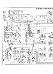
main schematic diagram - schema de la platine principale - I-lap
main schematic diagram - schema de la platine principale - I-lap
main schematic diagram - schema de la platine principale - I-lap

Create successful ePaper yourself
Turn your PDF publications into a flip-book with our unique Google optimized e-Paper software.
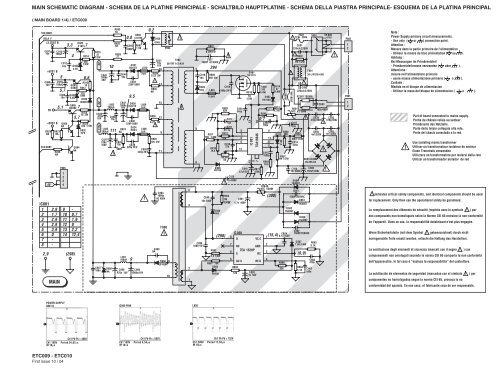
MAIN SCHEMATIC DIAGRAM - SCHEMA DE LA PLATINE PRINCIPALE - SCHALTBILD HAUPTPLATINE - SCHEMA DELLA PIASTRA PRINCIPALE- ESQUEMA DE LA PLATINA PRINCIPAL( MAIN BOARD 1/4) / ETC009STA NDBYRELA Y+3.3VST BC01110nC00810nSTA NDBY+5VST B5V+5VST BR829NA8VIC80112345678C013100uFC010100uFR827NAR828NA2,91,72,92,93,90--MAIN+C01210nC00910n+Q806NAP80512343,34D0033.9VQ001D882D0025.6VQ805SD882Q804NAQ002C1815R0146801/4WR01310R0122201/4WD8341N4001R82510 2WR826330 1/4WD8325V675 6,65,75,1910111213142,9 (298)75,7-0,71,902,212,4R015471/2W112v 8V9VC849470u16VC867100nC8451000u25V+L802100uHC827220u160V10++L803100uHD866NAC84810n111!R8931KR850NA+R85527C8421000u16V+D831RU4 YXD830RU3 YXQ850C1815C84410nC843220P 500VC840220P 500VD824R824 RU3 CNAC82610n500VL861100uHC868470u 16V0,8C8651000P9,5C830220p 2K V9R8921.5KL8102uHL8092uHL8082uHC839220p 2K V+C8661000u/16V!0,2D8504148+ C85110u16V16R8340.22 2W!R835NA1415R836120.22 1W!9R820120 2WC869NA11C8941000pAC 400VT860!P804D868 6UF 4004T80236-TRF 112-A X110!!53213186C81810nD8051HBC890100P/1K VR8378.2M 1WC8371000P AC400VR80956K 2WL8010.6uHR81115K 1/4WC86010n 500V294R8107K 5D806FR104D8601H8R8622.2 1/4WR861 75KD865FR102C819560p 2K VR80382KC81210nC8111nR81256KC81022pVR 8015K!(298)!R8601M1/4WC8251n 400V8765C820560pD513612IC 860R865120Q801SK 3115R8151K1/2W13C81647uF/25VC8614.7u 400VAU X914+10IC 801TDA16846+7R817470KVC CNCGNDTEA 1520PSRC+ C8931u 50VRE GR808 R814100 471/4W 1/4WD8071N4148R84112K0,7C850100n4R8041K 81182C8151000pRT8 60NTC 5OHM1234(300)R8134.7M(15,4)D8104148JP880R80656KR8071M 1/2WC8640.1uF/63VR86833K!!JP881/NAF801T2AL 250VC801220n/AC250V!R8021M 1/2WC802220n/AC250VRT 801 20OHMR801NTC 4.7 OHMC81710nR8054M7 1/2WC814220nC80810n 500VD8641N4007C891R8645.1K!!1500P/250VACD8611N4007D8621N4007D8631N4007C8921500P/250VACD8677.5K/1/4W(0,9)S801T80136-LIF010-A X0D801-D804RL 255 X4+ C806150uF/400vC862100nC803100n/400VC834470p/400V!C8044n7/250VR8639.1KC863470p1 2!VR 800471VC833470p/400vC8054n7/250v!!P80212P80112Note :Power Supply primary circuit measurements.- Use only ( or ) connection point.Attention :Mesure dans <strong>la</strong> partie primaire <strong>de</strong> l'alimentation- Utiliser <strong>la</strong> masse du bloc alimentation ( ou ).Achtung :Bei Messungen im Primärnetzteil- Primärnetzteilmasse verwen<strong>de</strong>n ( o<strong>de</strong>r ).Attenzione :misure nell'alimentatore primario- usare massa alimentazione primario ( o ).Cuidado :Medida en el bloque <strong>de</strong> alimentacion- Utilizar <strong>la</strong> masa <strong>de</strong>l bloque <strong>de</strong> alimentacion ( o ).!Part of board connected to <strong>main</strong>s supply.Partie du châssis reliée au secteur.Primärseite <strong>de</strong>s Netzteils.Parte <strong>de</strong>llo te<strong>la</strong>io collegata al<strong>la</strong> rete.Parte <strong>de</strong>l chasis conectada a <strong>la</strong> red.Use iso<strong>la</strong>ting <strong>main</strong>s transformerUtiliser un transformateur iso<strong>la</strong>teur du secteurEinen Trenntrafo verwen<strong>de</strong>nUtilizzare un transformatore per iso<strong>la</strong>rvi dal<strong>la</strong> reteUtilizar un transformador ais<strong>la</strong>dor <strong>de</strong> red! Indicates critical safety components, and i<strong>de</strong>ntical components should be usedfor rep<strong>la</strong>cement. Only then can the operational safety be garanteed.Le remp<strong>la</strong>cement <strong>de</strong>s éléments <strong>de</strong> sécurité (repérés avec le symbole ! ) par<strong>de</strong>s composants non homologués selon <strong>la</strong> Norme CEI 65 entraine <strong>la</strong> non-conformité<strong>de</strong> l'appareil. Dans ce cas, <strong>la</strong> responsabilité dufabricant n'est plus engagée.Wenn Sicherheitsteile (mit <strong>de</strong>m Symbol ! gekennzeichnet) durch nichtnormgerechte Teile ersetzt wer<strong>de</strong>n, erlischt die Haftung <strong>de</strong>s Herstellers.La sostituzione <strong>de</strong>gli elementi di sicurezza (marcati con il segno ! ) concomponenenti non omologati secondo <strong>la</strong> norma CEI 65 comporta <strong>la</strong> non conformitá<strong>de</strong>ll'apparecchio. In tal caso é “esclusa <strong>la</strong> responsabilità” <strong>de</strong>l costruttore.La subtitución <strong>de</strong> elementos <strong>de</strong> seguridad (marcados con el simbolo ! ) porcomponentes no homologados segun <strong>la</strong> norma CEI 65, provoca <strong>la</strong> noconformidad <strong>de</strong>l aparato. En ese caso, el fabricante cesa <strong>de</strong> ser responsable.POWER SUPPLYQ801 DIC860 PIN8L808111Ch1 100VM 10µsCh1 Pk-Pk = 408VPeriod 24,87µsCh1 100VM 10µsCh1 Pk-Pk = 502VPeriod 4,54µsCh1 200VM 10µsCh1 Pk-Pk = 732VPeriod 17,63µsETC009 - ETC010First issue 10 / 04
MAIN SCHEMATIC DIAGRAM - SCHEMA DE LA PLATINE PRINCIPALE - SCHALTBILD HAUPTPLATINE - SCHEMA DELLA PIASTRA PRINCIPALE- ESQUEMA DE LA PLATINA PRINCIPAL( MAIN BOARD 2/4 ) / ETC009SCANNING / DEFLECTIONVertical Deflection (pin 1 P400 )VD RAVD RBX- RA YAB LSA NDCA SEH-OUTE-WQ281BC 847C300100uF/50V+R3502K 2C3501500PD3042V4D3054148R286330-0,1R282-0,10R283270R3141KD3004148R3001K 2D28024VIN PUT1VCC0,8+14VC308220uF/25V+13D3063V9+C3512200PC307CA P POLR2805K 6+14VD2812,54148Q280BC 85719D601R285470D3074148R284100KR3161KD3084148C3134.7uF/50V+ C43147uF25VR401470+R40610KD413IN 40010,42D309IN 4001C405100nD4045V6R4071 1/2WPOMP UP GND OUT-11,5 -13 0,23+R40415K1W112V9V10,4D8334004+R402221WIC 300STV 93024C323100uF35VC360100uF/35V!R4132201/2WC4143300+C4225600p/63V33VP403R40311/2WC3250.33u5R3131 1W-14VC324100uF/25V4321T401R40815K1/4W+ C411100u160VD4054004+14V210Q402SC5885C4041000P500VVP6R4201.52W10913VREF70,8D C3342n2-14VC413470u/25V+14vC415470u 25vC40810U 250vD421RS3FSD422FR104+D403FR104-13+++13C409C4163300P1.6KVC403390P/500VD402FR104C412390p/500VD401FR104!D3204148R35110KR40931 1/2WR4051 1/2WR418390P 500VC4177600pF1.6KV-14V!1 1/2W61074291C41922001.6KVR3211.5112VT402C3371000PC420+10u 160vJP401!R3152K 2D400FR104R3242201WR41047K 1/4WC4210.39u/250vHVC3420.22uL41150uHEH TL4120uHR4111K 2WFO CU SSCRE EN8C410100n+14VR4151KP400CON4R41410KC4072n2To CRT12341111-10VCh1 20VM 10msCh1 Pk-Pk = 50VPeriod 20msSCANNING / DEFLECTIONHorizontal Deflection (pin 3 P400 )60V0Ch1 50VM 20µsSCANNING / DEFLECTIONVertical Deflection (PIN 2 P400 )Ch1 1VM 10msCh1 Pk-Pk = 108VPeriod 15,68µsSCANNING / DEFLECTIONPIN 1 Of IC300 (Input)Ch1 Pk-Pk = 1,8VCh1 1V Period 200µsM 20msCh1 Pk-Pk = 2,4VPeriod 20,16ms0Q401C2235C4011000P/500VC45010nD4505V6R45068KR4513.92WQ450IRF630L450600UHC4514.7uF50VC41822n400V1SCANNING / DEFLECTIONHorizontal Deflection (PIN 4 P400 )Ch1 Pk-Pk = 1040VCh1 500V Period 64µsM 40µsETC009 - ETC010First issue 01 / 06
MAIN SCHEMATIC DIAGRAM - SCHEMA DE LA PLATINE PRINCIPALE - SCHALTBILD HAUPTPLATINE - SCHEMA DELLA PIASTRA PRINCIPALE- ESQUEMA DE LA PLATINA PRINCIPAL( MAIN BOARD 3/4) / ETC009111SCL / SDASCLCh1 200mVM 400µsSCL / SDASDACh1 200mVM 100µsCVBSCVBS From Scart OutCh1 50mVM 20µsCh1 Pk-Pk = 508mVPeriod 11,13msCh1 Pk-Pk = 516mVPeriod 55,65µsCh1 Pk-Pk = 516mVPeriod 225,2nsETC009 - ETC010First issue 10 / 04RLVP961P964C9631nC9603n32468101214161820P9012468101214161820C9641nP901SIDE AVP960YCR9631001357911131517192113579111315171921C9382n2R90875D9048.2VD9058.2VD9068.2VR90933KR91175R913100R91475D9038.2VC909220PC918220PR91010KR91275R92147KP962=>P902C9641nC9651nD9008.2V+C963100uF+ C962100uFC9362n2D9018.2VD9028.2VVoR960220 R961220R962C9613n3100L9052.2uHL9062.2uHC9392n2C9432n2C9442n2P96287654321L9002.2uHR92022KR92347KR92433KP902R92510KR92675L9022.2uHD9078.2VD9088.2VP963=>P602P9631234C9372n2C9412n2C9422n287654321P6021234R91675R900330R901100kR902330R903100kR92222K5VR90547KR90747K0,1C910220PC919220PC9452n2C9462n2Q900BC 847C932220PP13000C902100pQ902BC 847C903100pC905R904 2.2uF22KC9062n2R9151kR9171kR90622kC9132n2C9152n2C916220PR91875+R927751KR930R93147KR93347K1KR932C9072n2C90410uF0 16VQ901 1,5BC 857C9110.1uF+C9122.2uFC9142.2uF+L9032.2uHR93575P1301234C933220P+C130220P+C9082.2uF+C9200.1uFC9302n2C9312n2C935220PJP130C90110uF16VR93475+-1+BST1GRFBST2R131220R130220 C131220PSDAQ903BC 837MSCLC20010uFAOUTLC2032.2uF+R21782kAOUTR+P201 R25247K1R2512 1KR250 1K3Vo5R203 100R202 100+5VC201220nC229100nR25347KL20410uHC2023n3R241 41390C234 421uF43Test1L205 C24710uH 2.2u/50vC235100nC22822nC2362.2uFC2372.2uFC2310.1uFC23322nC2391uFC2381uFR21882kR2251KC2304n7+++++R22068KR20147K33C2502.2uF34++C2512.2uF36++3537383940444546474849505152535455565758596061626364+5VC2042n2R2041KAV L32A.IN5LAGCR205680IFVEDIO OUTV CC8VEHTA.IN5RA.OUTSLA.OUTSRDECSDEMAU DEEMGND 2PLLI FSIFA GCDVB /FM OUTAG C2SI FVP2SVOA.IN4LA.IN4RCV BS4/Y4C4A.IN2LA.IN2RCV BS2/Y2A.IN3LA.IN3RCV BS3/Y3C2/C3A.OUTLA.OUTRA.OUT HLA.OUT HRCV BSOSVM6531R22110kSANDCASEAGC OUTFB ISO6630R2231k5VC268220pR222100C269220pC20522nFSIF2HOUT67H OUT2912SIF1GND com b6828GNDIF+5V comb69C2420.1uF+C24110uF16VL20610uH5VR20639K27C2431nIREFBIN70P20326C2441nVSCGI N7134VDRAVDRBC2670.1uFP203C20810uF16V+RC21022nFC206150n C211 220n25VIFIN2RIN72C2450.47u24R207100C207 C2091n 1nVIFIN1YSYNC7312345623VD RAYOUT7422VD RBUOUT75R208100C2131n21E-WVOUT76C240220pR20910020FBDE CBGINSSW 37719SECPL LR/PrIN 378C24622n18C24822nGGND 1G/YIN379C217100n+C2146n817C24922nIC201BC2640.1uFC26310uF16VR227120K+C21210uF16VC2152.2uF50VR21012KPH1LFB/P bIN 38016PH2LFGND 381ABL4C21610n15VP1LPF82+L20010uHC218100n14+L20710uHC2522n2R228220DECDIG3,3+13C25322uF16V R2294K 75VBCLIN83Q204BC 857C220C219 33P10uF16VVG/LEDBL KI N84+5V12D.GNDRO85D2045V 611XTALOUTGO862Q207BC 8572,720Q206BC 857R2301K5VC223100uFC221 10V+33P10C2702n2Z20024.576MHzXTALI NBO879vrefP_Sdac+3.3V analog88R27118KR27033KC255 C256220n 100nL20810uHQ208BC 857R2311K8VrefN_SdacVR EFAD_NEG89L201C222 1uH100n27R2321KVrefP_SdacVR EFAD_POS90L20910uH2,6+3.3V-S TB6VrefN_SdacVR EFAD91C258100nL2021uH5VrefP_SdacGND A9243.3VA3TDA1 2020HVDDA193+ C26547uF16VD2704148C254100PP202=>P502123456C224100n31.8VC4VDDA294P202L2101uHD2714148+5VST B+5VST BR213R215 R216R212 2.233K2.233k 1/2W 1/2W4,2 Q200 4,2R211 2,5 Q201 BC 327 2,5 Q202BC 847BC 8474k7R2141,9 4k71,9+ C22510uF16VC227 +C226L203100n 10uF 10uH16V2GNDC257100P1GNDSCAR T1 P3.1SCAR T2 P3.0ROTA TION P2.2TUNING P2.0SDA2 P1.3C260220nFSCL P1.6D2724148C259100PP2.3P2.13.3VSDA P1.7SCL2 P0.0IB O D/A P0.1IB O STB P0.2VSS953.3V-S TBGA ME L P1.5GA ME R P1.4LE D P0.3P0.4VSSC 2VDDC2TV STB P1.1IRQ P1.0VD D96P1.2GND1.8VP2.5MUTE P2.4GNDKE YB P3.3X-RA Y P3.2DECV1V81.8VIR P0.5C261220n5V128127126125L2111uH+ C26247uFC01810n+L00110uH124C017 C019100n 10uF123 16V122121120119118117C022220n116R038 100115R037114 100113112111L00210uHR26022kC028220nR04810KL00310uH2,5 Q210BSH 10322KR01722KR018R024100D0042V4L004 R26110uH 22K+R281150KC02447uF16VD007IN 4148R04622kQ209BSH 103R04015KR0391kC2811nD0064148D0054148110 C023R027 3K 3220nF+5VST BR025 100109R029 3K 3108R026 100R028 3K 3R041 100107R042 3K 3106R043 100R021 R044 1K100105R045 1KR035 100104+5VST B10310210110099989716VR0361K+3.3V STBR03447R0325K 6D2054148 +C28047uF16V+5VST B+5VST B+3.3VST B8VR03110KR26222K5R03010KC027100P123456Q203BC 327R0332K 2+5VST BSYSMU TEKEYX- RA YST1ST2RELA YC026100PaSDASCLP008P008LED-0,6 MR04747KP8051234bbIRccQ205BC 847STA NDBYa
MAIN SCHEMATIC DIAGRAM - SCHEMA DE LA PLATINE PRINCIPALE - SCHALTBILD HAUPTPLATINE - SCHEMA DELLA PIASTRA PRINCIPALE- ESQUEMA DE LA PLATINA PRINCIPAL( MAIN BOARD 4/4) / ETC009PowerK 001A. SEARCHK 002P+K 003P- VO L+ VO L- ME NU TV /A V D001K 004K 005K 006K 007K 008IR001P00154321IRLED+5VS TBKEYGND1AGCC100 +10uF16VAGCR0011K 5TU 100UV 1336VT2R10339kR10068kR10110kHi/n.c.3D100IN 4148C101100PR0021K+5VSCLMi/BS1(SCL )4R003680C104100PR104100SDALo/BS2(SDA)5R109100L10110uHR004470V+6C10210n+5Vi.c.(V+)7R0053904,9+ C103100uF10Vi.c.8C10547uF50V+R006300i.c.(+33V)9P001R007220R00847+P001(KDB)=>P001(MAIN)C10610nIFGND1033VD102BYV 79C33C11210n12345IF25IF11R113100R112330C10710nR114563C00147u/16VL1021uH2R1161KR117150C00210nR1114701R11533C10810nQ101C3779R11822+8vR12733L103220nHC10910nC11010nR12482R1292k21234C1131nL1041uHWPn.c.A2VssZ10040.4MHzR1196K 854321IC 00124C16Vd dPTCSCLSDAZ102K3953DZ102=> Z101D1051S110D1041S110Q102BC 847876C00356P5P001(MAIN)=>P001(KDB)Z101K9453DC00410nR12647KR125100k22C00556pP003R010R009225432122R0115VSTBR128220R1216K 8R1206K 8P003+5v43214321+ C11110uF/16VSCLSYSSDAETC009 - ETC010First issue 01 / 06
ETC009 - ETC010First issue 01 / 0614153216 896711101IC 600TEA2025B+C6061000uFR60110kR6004K 7R6024K 7C6010.22C6003300pC6050.22R60310KR5001.5KC5001nscreenAOUTRAOUTLR517470R516470 1/4WQ512BF422Q522BF422Q532BF422Q531BF422R527470R537470R53310R5201K 1/4WC531470PR51515KR5181.5K 1/2WR5281.5K 1/2WR5381.5K 1/2WQ513BF423Q533BF423Q523BF423R526470 1/4WR52515KR53515KR536470 1/4WQ521BF422Q511BF422R52310C521470PR51310C511470PR524270R514270D5114148D5214148R534270D5314148R52147R52210KR51147R51210KR53147R53210KD503BAV2 1D501BAV2 1D500BAV2 1D502BAV2 1123456P502=>P202 (MAIN)1234P503=>P4031P504EH TG1G2G3KBKGKRX 501TUBE+C50110uF 250VR503150KR50410+C50210uF 250VC6080.15C6110.154,5,12,1312P600=>12P601=>P602R5022.2MC6043300p+ C602100uF+C603100uF+ C607100uF+C612100uF/25V+C609100uF/25V+C610100uF/25V+C613100uF/25VJP601JP602R6052209V1212C61410nR6110.22/2WR60910KR610 10KD60041489V+C616100uFQ602C1815Q601A1 015R60810KMU TELRPML50110uHJP60325V25V25V25V25V1/2W2K V1W1W1WCRTMAINKEY BOARDS086P082+P083P081S083S082C082C081R088R080D081D081AR081R085 R084 R083R082J082543211212S085S084S081POWER+VOL-VOLCH+CH-MenuJ080J081P600P60114153216896711101IC600TEA2025B+C6061000uFR6013k3C6010.22C6003300pC6050.22R6033K3AOUTRAOUTLC6080.15C6110.154,5,12,1312P60012P601(P602)C6043300p+ C602100uF+C603100uF+ C607100uF+C612100uF/25V+C609100uF/25V+C610100uF/25V+C613100uF/25VJP601JP602R6124k79V12121215143138967412IC601TDA7266C61410nR6110.22/2WR60810KR60747K+C61510uF/25VR60647K8VR6131KD60141485VQ604BC847Q600BC857MUTELRPRLPP600P601JP60325V25V25V25VQ603BC847R6141KQ602BC847R61010KR60910KD6004148+ C616100uFQ601BC85716VMMR6154k7C622100n1215143 138 967412IC 601TDA 7266R60747K+C61510uF/25VR60647K9VRLPP600P601M2 x 6W versionCRTAUDIOAUDIO209,4209,4127,5124121,55,75,74,7209,4128,2209,42101252,62,82,12,22,62132200V200V200V200V1,6Vpp-H02,2V4 P5021,8Vpp-H02V3 P5021.Vpp-H02V5 P5021 P5022,8Vpp-V3V010msT=64µs88Vpp-HT=64µs80V-HT=64µsRGB80Vpp-HETC009
MAIN BOARD - PLATINE PRINCIPALE - CHASSIS GRUNDPLATTE - PIASTRA PRINCIPALE - PLATINA PRINCIPALCOMPONENT SIDE - COTE COMPOSANTS - BESTÜCKUNGSSEITE - LATO COMPONENTI - LADO COMPONENTESETC009 - ETC010First issue 10 / 04
VIDEO AMPLIFIER BOARD - PLATINE AMPLIFICATEURS VIDEO -VIDEOVERSTÄRKERPLATTE - PIASTRA AMPLIFICATORE VIDEO -PLATINA AMPLIFICADOR VIDEOCOMPONENT SIDE - COTE COMPOSANTS - BESTÜCKUNGSSEITE - LATO COMPONENTI - LADO COMPONENTESKBCOMPONENT SIDE - COTE COMPOSANTS - BESTÜCKUNGSSEITE - LATO COMPONENTI - LADO COMPONENTESAVCOMPONENT SIDE - COTE COMPOSANTS - BESTÜCKUNGSSEITE - LATO COMPONENTI - LADO COMPONENTESETC009 - ETC010First issue 01 / 06
VIDEO AMPLIFIER BOARD - PLATINE AMPLIFICATEURS VIDEO -VIDEOVERSTÄRKERPLATTE - PIASTRA AMPLIFICATORE VIDEO -PLATINA AMPLIFICADOR VIDEOSOLDER SIDE - COTÉ CUIVRE - LÖTSEITE - LATO SALDATURE - LADO DEL COBREKBSOLDER SIDE - COTÉ CUIVRE - LÖTSEITE - LATO SALDATURE - LADO DEL COBREAVSOLDER SIDE - COTÉ CUIVRE - LÖTSEITE - LATO SALDATURE - LADO DEL COBREETC009 - ETC010First issue 01 / 06
I - ENTER/EXIT SERVICE MODESERVICE-MODE - ALIGNMENT PROCEDURE EN1.1. Accessing Service Mo<strong>de</strong>A) Switch the TV set into the Standby Mo<strong>de</strong>.B) Switch off Power Supply.C) Switch on Power supply whilst pressing the magenta ”TEXT”key continuously until TV set switch on and enter service mo<strong>de</strong>.1.2. Page selectingPress 1,2....8 or 9 key of the RCU to enter page 1,2,...8 or 9 ofService Mo<strong>de</strong>.U03C00C 1.8 2005. 07 . 20-01ADR0 01111010 ADR1 01010000ADR2 10000010 ADR3 00011110AFC 00000000 RG 00110111GG 10110111 BG 00110111DEFL 00001111 DISC 128LAST NV : 1878ERR: 00000000REV: 8822041.3. Navigation:- Press ”Up” and ”Down” key to select option;- Press ”Left ” and ”Right ” key to adjust or select option.- All change in service mo<strong>de</strong> will be saved in EEPROM automatically1.4 Temporary exit from Service Mo<strong>de</strong>- Press ”9” key and select MODE 1.- Set D-MODE to ”Direct key enter enable” .- Press ”OK” KEY on the RC to exit or access to service menu.1.5. Exiting from Service Mo<strong>de</strong>- Press ”OK” KEY on the RC.Note : Before exiting from Service mo<strong>de</strong> check that D-MODE is set to ”Direct key enter disable” (see 1.4).1.6. Brief introduction on some special mo<strong>de</strong>s1.6.1. Aging Mo<strong>de</strong>It is used before set alignment and should operate in Service mo<strong>de</strong>;The TV set cannot enter standby after 15 minutes when no signal if the ”AGING” Mo<strong>de</strong> is selected.Press blue ”GUIDE” Key, the Aging Mo<strong>de</strong> will be entered when ”Aging Mo<strong>de</strong>” is shown on screen.Press blue ”GUIDE” key again will exit ” Aging Mo<strong>de</strong> ”.1.6.2. Vertical Stop mo<strong>de</strong>- it is used to adjust the screen voltage.Press red ”PRESETS” key and repress ”PRESETS” (red) key to exit.1.6.3. White ba<strong>la</strong>nce alignment mo<strong>de</strong>- Press ”EXIT” key on factory RCU, The set will disp<strong>la</strong>y ” BUS OPEN ”, which means the I2C bus from the CPU toother UOC3 module and ICs had been released. This is only used during automatic adjustment of white ba<strong>la</strong>nce.Press other key will exit ” BUS OPEN ”.1.6.4. Reset- Initialization before the set will took away from factory.In factory mo<strong>de</strong>, press ”INFO” (P
III - ALIGNMENT PROCEDURENotes: - Alignment should be done after 3 minutes warm up of TV .3.1. B+ VOLTAGESB+ Voltage ETC009: VR801ETC010: -(no alignment)Standard TV - Settings :CRT typeB+ Voltage+ + =50%IRICO A36CPAA 00X02 108V +/- 0.5VV=TTD A51ELD 032X004 112V +/- 0.5VTV to AV1 : B<strong>la</strong>ck testDP805 (ETC010)DP824 (ETC009) LGPD A51ERS 357X440 (SLIM)patternZHONGHUA CHA34AGT13X53 108V +/- 0.5VTTD ELM021X001 130V +/- 1.5VTTD W76ELC011X001 132.5V +/- 1.5V3.2. RF AGC3.2.1. Method 11) Input 60dB PAL BG , with half-Color Bar signal2) Press key "2" to enter page 2 of factory mo<strong>de</strong> (Fig.1)3) Select RF AGC with " up " or " down " key. .4) Press "ZOOM- "(left) and " ZOOM+ " (light) keyuntil the hint disp<strong>la</strong>y just change from "Inactive" to"active".)5) Adjust AGCL for SECAM L /L' same as the PAL.3.2.2. Method 21) Apply RF signal of 210.25MHz (BG CH 10) modu<strong>la</strong>tedwith color bar at 3mVrmx to Tuner input2) Tune to CH103) Go to factory mo<strong>de</strong>, entry page 2 (Fig.1) & set"RF AGC" to 00 (max IF output).4) Monitor 38.9MHz IF frequency response at Tunerpin11 with spectrum analyzer by using high impedanceprobe or equivalent.5) Increase RF AGC control until IF frequency response8 +1/-2 d B down from maximum.210.25 MHz3mVU0C300C 1 . 8 2005. 07 . 20-015VPOS 245VAM 295VSL 385VL 305VSC 315VSCL 34RF AGC 14AGCL 14Fig.1antennainputActivepage 2chassis ETC009/ETC010Tuner11IFBG CH 10Monitor IF38.9 MHz3.3. CRYSTAL OSCILLATOR FREQUENCYNotes: - If TV had NICAM function, we recommend to adjust crystal with NICAM.3.3.1. Crystal oscil<strong>la</strong>tor frequency adjustment with NICAMa) Apply PAL BG NICAM signal with good reception quality.b) Enter factory mo<strong>de</strong>, press "Vol -"(FORMAT) key ,it will disp<strong>la</strong>y " DCXOAUTO " , (Fig.2) then press "ZOOM+" (light)key to start auto adjust , when it disp<strong>la</strong>ys "DCXOAUTO OK" ,the adjust is finished .3.3.2. Crystal oscil<strong>la</strong>tor frequency adjustment without NICAM( for software with UOC3 TDA12070/12072 only )a) Input PAL color bar signal.b) Enter factory mo<strong>de</strong>, press "Vol -"(FORMAT) key ,it will disp<strong>la</strong>y " DCXOAUTO " , then press "ZOOM+"(light) key to start auto adjust , when it disp<strong>la</strong>ys "DCXOAUTO OK" ,the adjust is finished .3.3.3. Crystal oscil<strong>la</strong>tor frequency adjustment without NICAMa) Input PAL color bar signal.b) In factory mo<strong>de</strong>, press "0" to entry page 0 , (Fig.3).Adjust "DCXO CAP" until disp<strong>la</strong>y " DISC " is steady at 128.U0C300C 1 . 8 2005. 07 . 20-01DCXOAUTOFig.2U0C300C 1 . 8 2005. 07 . 20-01YDFE PAL 15DEC LVL 2MONO LVL 0NIC LVL 0SAP LVL 0SAP LVL 0ADC LVL 27DCX0 CAP 56 DISC: 128PSCALE 0.375 DCX0:61PLIM 96PCENTER 12LOUDNESS 3DUB100Hz 6Fig.3page 0ETC009 - ETC010First issue 01 / 06
Notes: - Alignment below should be done after 15 minutes warm up of TV.3.4. G2 & FOCUSU G2Screen voltageadjustmentG2 potentiometer :SCREENFocus-BlockStandard TV - Settings :+ + = 50%TV to AV1 : B<strong>la</strong>ck testpattern1- Press red "PRESETS" (Led)Key on the remote contro<strong>la</strong>nd the screen will become ahorizontal line,2- adjust the "screen voltage"of the fly back transformeruntil the horizontal line canjust be seen barely(minimum visible intensity).No correct Correct :minimum visibleintensityFOCUSFOCUSVRFocus-BlockStandard TV - Settings :+ + = 50%TV to AV1Test patternSharp picture3.5. SUB COLORa) Input NTSC Vi<strong>de</strong>o pattern : AVb) Press key "4" : page 4. (Fig.4).Measure at the CRT blue Catho<strong>de</strong> (Fig.5).c) Adjust COLC to make level a and d equal;then TNTC to make level b and c equal;d) Input PAL color bar signal.e) Adjust COLP to make level of a,b,c,d equal ;f) Input SECAM color bar signal, and adjustCOLS to make level of a,b,c,d equal.3.6. WHITE BALANCEU0C300C 1 . 8 2005. 07 . 20-01VOL 01 30VOL 10 104VOL 90 170VOL 100 188CNTC 31BRTC 30COLC 23TNTC 35COLP 3COLS 23SHPTV 32Fig.4 page 4BlueCatho<strong>de</strong>a b c dCRTAFig.5White Ba<strong>la</strong>nce adjustment (neutral)a) Input RF B<strong>la</strong>ck and White pattern signal (PAL).b) Press "1" key to enter white ba<strong>la</strong>nce adjustment (Page 1:Fig.6)c) Measure the dark si<strong>de</strong> of the picture with a color analyzer.Adjust RED and GRN until the data on the analyzerbecome x=284 +/-8, y=299 +/-8.d) Measure the bright si<strong>de</strong> of the picture.Adjust WPR, WPG and WPB until the data on the analyzerbecome x=284 +/-8, y=299 +/-8.e) Repeat step c and d until you get right white ba<strong>la</strong>nceon both dark and bright si<strong>de</strong> of the screen.f) Input RGB B<strong>la</strong>ck and White pattern signal (PAL).g) Measure the dark si<strong>de</strong> of the picture with a color analyzer.Adjust REDC and GRNC until the data on theanalyzer become x=284 +/-8, y=299 +/-8.h) Measure the bright si<strong>de</strong> of the picture.Adjust WPRC and WPGC and WPBC until the data on theanalyzer become x=284 +/-8, y=299 +/-8.i) Input SECAM L B<strong>la</strong>ck and White pattern signal.j) Measure the dark si<strong>de</strong> of picture with a color analyzer,Adjust REDSECAM and GRNSECAM until the data onthe analyzer become x=284 +/-8, y=299 +/-8.Warm color temperaturea) Press green " LIST" key .b) item: Warm R ; Warm G ; Warm B : Factory adjustc) Check the item values are as shown opposite.Alignment of Cool color temperaturea) Press green " LIST" key.b) item: Cool R ; Cool G ; Cool B : : Factory adjustc) Check the item values are as shown opposite.U0C300C 1 . 8 2005. 07 . 20-01WPR 26 GRNC 40WPG 29 WPRC 18RED 31 WPB 31 WPGC 18GRN 29 REDC 32 WPBC 15greyU0C300C 1 . 8 2005. 07 . 20-01Warm R 10Warm G 10Warm B 10Cool R 10Cool G 10Cool B 10page 1Fig.6ETC009 - ETC010First issue 01 / 06
3.7. SUB BRIGHTNESS3.7.1. Sub brightness adjustment1) Input eight steps gray signal.2) Press key "4" to enter sub-brightness adjustment.3) Adjust "BRTC" until the secondary gray bar just to be seen.(Fig.7).U0C300C 1 . 8 2005. 07 . 20-01VOL 01 30VOL 10 104VOL 90 170VOL 100 188CNTC 31BRTC 30COLC 23TNTC 35COLP 3COLS 23SHPTV 32The 2nd gray scaleFig.7page 43.8 PICTURE GEOMETRY ADJUSTMENT3.8.1. Vertical geometry items- Press key "2" to enter Vertical geometry adjustment.U0C300C 1 . 8 2005. 07 . 20-015VPOS 245VAM 295VSL 385VL 305VSC 315VSCL 34RF AGC 14AGCL 14Active5VSL(V-Slope)5VAM(V-Amplitu<strong>de</strong>)VERTICAL GEOMETRY ITEMS5VL(V-Linearity)5SCL(VerticalS-Correction)Spage 25VPOS(V-Position)5VX*(VerticalOver scan)* According to Software3.8.2. Horizontal geometry items- Press key "3" to enter Horizontal geometry adjustment.U0C300C 1 . 8 2005. 07 . 20-015HSH 365PAR 245BOW 225EWW 335EWP 355UCR 425LCR 325EWT 365WBR 75WBF 7page 35HSH*(H-Position)5PAR*(Parallelogram)5BOW*(Bow Adjust.)HORIZONTAL GEOMETRY ITEMS5UCR(EW-UpperCorner)5LCR(EW-LowerCorner)5EWT(EW -Trapezium)5EWW(H-Amplitu<strong>de</strong>)5WBR**End ofB<strong>la</strong>nking5EWP(Pincushioncorrect.)5WBF**Start ofB<strong>la</strong>nking* Only valid for ETC009 except mo<strong>de</strong>ls with Slim CRT** Only valid with 16:9 tubesETC009 - ETC010First issue 01 / 06
0,8MHz0,8MHz0% 20%0% 20%1,8MHz1,8MHz2,8MHz3,8MHz40% 60% 80%2,8MHz3,8MHz4,8MHz40% 60% 80%100%4,8MHz100%3.8.3. AdjustmentsSignal : 4/3 test pattern - Cross hatch pattern (PAL or SECAM), NTSC signal to adjust NTSC geometry.4/3 picture tube4 / 3standard mo<strong>de</strong>Overscan V=107% , H=107%Vertical adjustment : press ”2”1- Check the Factory adjust 5VSC = 31; Adjust Vertical Slope : 5VSLCorrectNo correct2- Adjust Vertical Position (5VPOS) , Vertical amplitu<strong>de</strong> (5VAM).3- Adjust Vertical Linearity (5VL) and S correctionHorizontal adjustment : press ”3”1- Adjust Horizontal Position (5HSH) and Horizontal parallelogram (5PAR),2 -Adjust Horizontal Bow (5BOW)3 -Adjust Horizontal width (5EWW) and Pincushion correction (5LCR)S4 -Adjust EW Amplitu<strong>de</strong> (5EWP) , EW Upper (5UCR) / Lower Corner (5LCR)5 -Adjust Trapezium correction (5EWT)16/9 picture tubeOverscan V=107% , H=107%Vertical adjustment : press ”2”1- Check the Factory adjust 5VSC = 31; Adjust Vertical Slope : 5VSL16 / 9standard mo<strong>de</strong>CorrectNo correct2- Adjust Vertical Position (5VPOS) , Vertical amplitu<strong>de</strong> (5VAM).3- Adjust Vertical Linearity (5VL) and S correctionHorizontal adjustment : press ”3”1- Adjust Horizontal Position (5HSH) and Horizontal parallelogram (5PAR),2 -Adjust Horizontal Bow (5BOW)3 -Adjust Horizontal width (5EWW) and Pincushion correction (5LCR)S4 -Adjust EW Amplitu<strong>de</strong> (5EWP) , EW Upper (5UCR) / Lower Corner (5LCR)5 -Adjust Trapezium correction (5EWT)Overscan V=107% , H=77%4 / 3 centered1 - Check the 16 / 9 standard mo<strong>de</strong> geometry.2 - Adjust H. width 77% (5EWW) and pincushion correction (5LCR)3 - Adjust if necessary lower/upper corner (5UCR/5LCR)4 - Adjust if necessary the Bow correction (5BOW) and parallelogram (5PAR).5 - Adjust 5WBF 4/3 and 5WBR 4/3to make the castel<strong>la</strong>tion just un-visible.Overscan V=122% , H=90%14 / 91 - Check the 16 / 9 standard mo<strong>de</strong> geometry.2 - Adjust H. width 90% (5EWW) and pincushion correction (5LCR)3 - Adjust if necessary lower/upper corner (5UCR/5LCR)4 - Adjust if necessary the Bow correction (5BOW) and parallelogram (5PAR).5 - Adjust 5WBF 14/9 and 5WBR 14/9 to make the castel<strong>la</strong>tion just un-visible.3.9 RESET TVWhen all item alignment is finished, please make the TV to RESET as 1.4.4.ETC009 - ETC010First issue 01 / 06
IV - FACTORY ALIGNMENT VALUESKEY 1 KEY 2 KEY 3 KEY 4Item Data Item Data Item Data Item DataRED 32 5VPOS 32 5HSH 42 VOL 01 30GRN 32 5VAM 23 5PAR 33 VOL 10 104WPRWPB32325VSL5VL28305BOW5EWW2939VOL 90VOL 100170188( ETC009 5W)194(ETC010 6W)WPG 32 5VSC * 31 5EWP 34 CNTC176(ETC010,10W)31(ETC009)21( for 14”15”)31(ETC010)REDC 32 5SCL 31 5UCR 46 BRTC 30GRNC 32 RF AGC 22 5LCR 43 COLC 23WPRC 32 5EWT 26 TNTC 35WPGC 32 AGCL 22 5WBR 7 COLP 3WPBC 325WBF 7 COLS 23REDSECAM 32 SHPTV 32GRNSECAM 32* No adjustableV - SERVICE MODE VALUES5.1 Analog control adjustmentPress key "5" to enter analog adjustment.KEY 5ItemDataETC009 ETC010CNTX Max. Contrast value 63 63CNTN Min. Contrast value 1 3BRTX Max. Brightness value 63 63BRTN Min. Brightness value 15 15COLX Max. Color value 50 50COLN Min. Color value 0 0TNTX Max. Tint value 63 63TNTN Min. Tint value0 0SHPX Max. Sharpness value 63 63SHPN Min. Sharpness value 0 05.2 - Picture item adjustmentPress key "6" to enter analog adjustment.DataItemETC009ETC010CPFK PAL Peaking value32 32CFPEK PAL PAL peaking frequency & value 3.5M 143NS 3.5M 143NSCFPEK NTS NTS peaking frequency & value 3.1M 160NS 3.1M 160NSCFPEK YUV YUV peaking frequency & value 4.0M 125NS 4.0M 125NSIFPL IF Offset 32 32BBTC Base-band tint control (phase U,V signal) 32 32PGR Original value of R 55 55PGG Original value of G 55 55PGB Original value of B 55 55ON VAM (<strong>de</strong>pends on tube)3 ( <strong>de</strong>pends on tube) 0VG2BRI Brightness of V line when adjust G2 20 20HDOL RGB drive gain.3 4`5.3 - OSD Position adjustmentPress key "7" to enter analog adjustment.ETC009 - ETC010First issue 01 / 06ItemDataOSD BRI OSD brightness 8CC BRI Teletext brightness 55CCD H Position for Teletext 115CCD V Position for Teletext 405OSD H OSD H position 95OSD V OSD V position 325MENU V Menu V. position 555MENU H Menu H. position 10
5.4 - Option adjustmentPress key "8" to enter Option adjustment.U0C300C 1 . 8 2005. 07 . 20-01OP01 00001110OP02 10000100OP03 00010011OP04 00000000OP05 00100111OP06 00001011OP07 11000011OP08 00000000OP09 00001100OP010 00110000ItemBit 7DataOP01 00001110OP02 10000100OP03 00010011OP04 00000000OP05 00100111 (10100111 for TDA12070/12072/H/N1F00)OP06 00001011 (00000100 for TDA12070H/N1F00)OP07 11000011OP08 00000000OP09 00001100OPT010 0011000000001110Bit 0Fig.8Check the bytes values. They indicate the configuration of the chassis and are given for information only.The <strong>de</strong>fault values are indicated in the follow table.- Choose the item Op01 ,Op02 ... by pressing up/down key.- Access to the selected Option adjustments by pressing ”Left” or ”Right” keyOP01U0C300C 1 . 8 2005. 07 . 20-01FMWS0/1 450kHzAGN 6dBAGC0/1 NormalAVLM Normal gainCMCA Stereo mo<strong>de</strong>MAT Adapted to standardOP01 : <strong>de</strong>fault value : 00001110Bit 0 - Bit 1: FMWS0/1 (Band width FM; 10: 450kHz)Bit 2 : AGN (Audio output amplitu<strong>de</strong>; 1: +6dB gain)Bit 3-Bit 4 : AGC0/1 (AGC time content selection; 01: Normal)Bit 5 : AVLM (Gain for analog FM <strong>de</strong>co<strong>de</strong>r; 0: Normal gain)Bit 6 : CMCA (stereo/mono- 0: stereo 1: mono)Bit 7 : MAT (Y,U,V to RGB matrix selection - 0:adapted to standard).OP02U0C300C 1 . 8 2005. 07 . 20-01MUS japanase matrixCB FSCCHSE0/1 -37dBCL0 4.29MHzDTR single chroma trapSDC Duty cycle 55:45HC0 EHT traking on vertical and EWOP02 : <strong>de</strong>fault value : 10000100Bit 0 : MUS (Y,U,V to RGB matrix selection).Bit 1 : CB (Select. for center of chroma band; 0: Fsc)Bit 2-Bit 3 : CHSE0/1 (Sensivity of color killer; 01: -37dB)Bit 4 : CL0 (center frequency of SECAM bell filter; 0: 4.29MHz)Bit 5 : DTR (Dual Chroma trap; 0: single chroma trap) .Bit 6 : SDC (Hor. drive pulse width; 0: Duty cycle 55:45).Bit 7 : HC0 (EHT tracking only vertical or vertical and EW).OP03U0C300C 1 . 8 2005. 07 . 20-01OP03 : <strong>de</strong>fault value : 00010011MVKFBCEVBSLGACLIFSGD L IMacro vision key activeoff with fix beam currentNorman vertical b<strong>la</strong>nking280uANot activeNormalNo group correctionBit 0 : MVK (Macro Vision Keying; 1: active).Bit 1 : FBC (switch-off with b<strong>la</strong>nked RGB outputs or fixed beam current)Bit 2 : EVB (normal Vert. picture or exten<strong>de</strong>d vertical b<strong>la</strong>nking)Bit 3-Bit 4 : SLG0-SLG1 (selection of AKB b<strong>la</strong>ck current; 10: 280uA)Bit 5 : ACL (control the ratio of chroma/color burst; 0: Not active).Bit 6 : IFS (IF sensitivity; 0: Normal).Bit 7 : GDLI (group correction/group <strong>de</strong><strong>la</strong>y correction switch for L and I.0: No group correction).OP04U0C300C 1 . 8 2005. 07 . 20-01FFI Normal time constantBPB Normal operationBPB2 bandpass filterSSL 50%FSL <strong>de</strong>pen<strong>de</strong>nt on noise <strong>de</strong>tectorNo use OFFOP04 : <strong>de</strong>fault value : 00000000Bit 0 : FFI (IF PLL lock time constant, used for over modu<strong>la</strong>tion).Bit 1 : BPB (sound bandpass - filter for mono 0: Normal operation).Bit 2 : BPB2 (stereo band pass - filter for stereo/dual 0: active).Bit 3 : SSL (slice level of Hor. syn. Pulse; 0: 50%).Bit 4 : ACL (slice level of Vert. syn. Pulse; 0: <strong>de</strong>pendant on noise<strong>de</strong>tector).Bit 5,6,7 : No useETC009 - ETC010First issue 01 / 06
OP05U0C300C 1 . 8 2005. 07 . 20-01VAI Amplitu<strong>de</strong> 12%VA0/VA1 Amplitu<strong>de</strong> +5%FC0 OFFVG2 MODE LIGHT LINEDSS Normal operationDSG 0dBOP06U0C300C 1 . 8 2005. 07 . 20-01DCXOMUX NicamQSS QSS Amp activeFMI Output conn to QSS0NICAM ONRPA0/1 1:1RP00/1 1:1OP05 : <strong>de</strong>fault value : 00100111Bit 0 : VAI (gain correction; 0: no correction 1: +12% PAL I).Bit 1-Bit 2 : VA0/VA1 (IF CVBS output amplitu<strong>de</strong> correction; 10: +5%).Bit 3 : OFB (Offset control on Red and Blue channel).Bit 4 : FCO (force color on when bad signal, color killer not active).Bit 5 : VG2 MODE (0:OSD indication 1:Line).Bit 6 : DSS (0: normal operation 1: LCD / PscanBit 7 : DSG (audio output selection amplitu<strong>de</strong>; 0: 0dB)OP06 : <strong>de</strong>fault value : 00001011Bit 0 : DCXOMUX (0:P3DCX0 TDA12070/12072/without NICAM1: NICAM).Bit 1 : QSS (validation QSS amplifier; 1: active).Bit 2 : FMI (connexion QSS AMP output to SSD module or soundPLL <strong>de</strong>modu<strong>la</strong>tor; 0: Output conn to QSS0).Bit 3 : NICAM (NICAM selection; 1: ON)Bit 4-Bit 5 : RPA0 /1 (00)Bit 6-Bit 7 : RPO0/1 (00)OP07U0C300C 1 . 8 2005. 07 . 20-01PWL 3SOC0/1 0% above PWLPWL ON PWL circuit activeGD BG DK Group <strong>de</strong><strong>la</strong>y correctionOP07 : <strong>de</strong>fault value : 11000011Bit 0-1-2-3 : PWL (peak white limit; <strong>de</strong>fault : 3)Bit 4-Bit 5 : SOC0/1 (% above PW level; 00: 0% above PWL).Bit 6 : PWL ON (activation of the peak white limiting circuit; 1: active)Bit 7 : GD BG DK (activation of the Group <strong>de</strong><strong>la</strong>y correction;0: group correction)OP08U0C300C 1 . 8 2005. 07 . 20-01No useOFFOP08 : <strong>de</strong>fault value : 00000000Bit: OFF (No use)OP09U0C300C 1 . 8 2005. 07 . 20-01AFG FalseTYUV1 FalseBPBS TrueCLF TrueBWYC FalseCBPS FalseSLD FalseOSB FalseOP10U0C300C 1 . 8 2005. 07 . 20-01BKC FalseTYUV0 FalseQDT FalseTCCON TrueTCI2X TrueTXTS FalseBlue SCN FalseOP09 : <strong>de</strong>fault value : 00001100Bit 0 : AFG (AFC measurement; 0: AFC False)Bit 1 : TYUV1(Analog output selection for text; valid if TYUV0=1)Bit 2 : BPBS (Enable bypass of sound filter at stereo mo<strong>de</strong>)Bit 3 : CLF (Comb filter dio<strong>de</strong> c<strong>la</strong>mp; set to1)Bit 4 : BWYC (Bandwidth of anti aliasing filter at YC mo<strong>de</strong> of3.58MHz systems; 0: False)Bit 5 : CBPS (Internal chroma bandpass filter mo<strong>de</strong>; 0: False)Bit 6 : SLD (Sleep mo<strong>de</strong> <strong>de</strong>tector status; 0: sleep enabled, False)Bit 7 : OSB (width of Burstkey; 0: False burstkey=3.52us)OP10 : <strong>de</strong>fault value : 00110000Bit 0 : BKC (Internal burst key position; 0: False normal position)Bit 1 : TYUV0 (TXT/CC output selection; 0: False, RGB format)Bit 2 : QDT (Q values of Second chroma trap; 0: False)Bit 3 : FBC1 (Fixed beam current during switch off; 0: False, 1mA)Bit 4 : TCCON (Top sync. c<strong>la</strong>mp control; 1: True , active)Bit 5 : TCI2X (Top sync. c<strong>la</strong>mp time constant; 1: True)Bit 6 : TXTS (TXTS Mo<strong>de</strong> : TEXT source; 0: False TXT from CVBS)Bit 7 : Blue SCN (Blue screen with no signal; 0: False)ETC009 - ETC010First issue 01 / 06
5.5 - Mo<strong>de</strong> adjustmentPress key "9" to enter Mo<strong>de</strong> adjustment.U0C300C 1 . 8 2005. 07 . 20-01MODE 1 00110101MODE 2 10010111MODE 3 00000000MODE 4 11111101MODE 5 11000000MODE 6 10001100MODE 7 01110010MODE 8 00101000MODE 9 11001000MODE10 00100000ItemDataMODE 1 010110100MODE 2 10011111 (10011011 for TDA12070/12072 without L standard)MODE 3 00000000MODE 4 11111101MODE 5 01000000MODE 6 10001100MODE 7 01110010MODE 8 00000000MODE 9 11001000MODE 10 00110000Bit 700001110Bit 0Check the bytes values. They indicate the configuration of the chassis and are given for information only.The <strong>de</strong>fault values are indicated in the follow table.- Choose the item MODE 1 ,MODE 2 ... by pressing up/down key.- Access to the selected MODE adjustments by pressing ”Left” or ”Right” keyMODE 1U0C300C 1 . 8 2005. 07 . 20-01D-MODE Direct Key enter disabledAV OUT Always TVNO SIG. Mute when no signalMUTE AV0 Don't mute AV-OutNI ADISP OFFSEARCH FastTUNER CP OFFTXT FIN OFFMODE 2MODE1 : <strong>de</strong>fault value : 10110100Bit 0Bit 1Bit 2Bit 3Bit 4Bit 5Bit 6Bit 7: D-MODE (Direct enter D-mo<strong>de</strong> (Service mo<strong>de</strong>) with ”OK” key0:enable 1:disable): AV OUT (0: Always TV - 1: Follow source): No Signal (0: Demute when no signal - 1 mute when no signal): MUTE AV0 (Mute AV-out): NI ADISP (1: Nicam auto <strong>de</strong>tection OSD disp<strong>la</strong>y enable): SEARCH (Auto search speed setting): TUNER CP (CP bit selection of tuner): TXTFIN (TXT fine tuning selection)U0C300C 1 . 8 2005. 07 . 20-01SOUND DK ONSOUND BG ONSOUND M OFFDEF SND BGMAX PROG 100 ProgAUTO SND Request auto soundMODE 3U0C300C 1 . 8 2005. 07 . 20-01DBB/DVB DVBAVL OFFTilt OFFCOMBFILT OFFVM OFFSecam OFFSuperRec OFFMODE 2 : <strong>de</strong>fault value : 10011111Bit 0 : SOUND DK (<strong>de</strong>pends on requirement)Bit 1 : SOUND BG (<strong>de</strong>pends on requirement)Bit 2 : SOUND L (or I)* (<strong>de</strong>pends on requirement)Bit 3 : SOUND M (or I)* (<strong>de</strong>pends on requirement)Bit 4 - Bit5 : DEF SOUND (00: DK; 01: BG; 10: I; 11:M)Bit 6 : MAX PROG. (0: 100, 1:200 (no used))Bit 7 : AUTO SND (Request auto sound <strong>de</strong>tect when auto searching(0: Don’t request 1: request auto sound)* according mo<strong>de</strong>lsMODE 3 : <strong>de</strong>fault value : 00000000Bit 0-Bit 1 : DBB/DVB (Woofer 00:DVB; 01:DB; 10: Woofer, 11:OFF)Bit 2 : AVL (0: OFF)Bit 3 : Tilt (0: OFF)Bit 4 : COMB (Comb filter : 0: OFF)Bit 5 : VM (0:OFF)Bit 6 : SECAM (0:OFF)Bit 7 : SUPERREC (0:OFF)MODE 4U0C300C 1 . 8 2005. 07 . 20-01IF Freq 38.9MHzAV1 ONAV2 ONAV3 ONS-VIDEO1 ONS-VIDEO2 ONRGB ONMODE 4 : <strong>de</strong>fault value : 11111101Bit 0-Bit 1 : IF FREQ (00:45.75MHz; 01:38.9MHz; 10: 38MHz)Bit 2 : AV1 (1:ON) (<strong>de</strong>pends on requirement)Bit 3 : AV2 (1: ON) (<strong>de</strong>pends on requirement)Bit 4 : AV3 (1: ON) (<strong>de</strong>pends on requirement)Bit 5 : S-VIDEO1 (1: ON) (<strong>de</strong>pends on requirement)Bit 6 : S-VIDEO2 (1: ON) (<strong>de</strong>pends on requirement)Bit 7 : RGB (1: ON) (<strong>de</strong>pends on requirement)ETC009 - ETC010First issue 01 / 06
MODE 5U0C300C 1 . 8 2005. 07 . 20-01RADIO OFFEQ BAR Equalizer BarBCFCHECK ON MODE 5 : <strong>de</strong>fault value : 01000000Bit 0,1,2,3,4 : No useBit 5 : Radio (FM Radio 0:OFF)Bit 6 : EQ BAR (User menu disp<strong>la</strong>y (0: bass & Treble; 1:Equalizer)Bit 7 : BCF CHEK (Beam current protection 1:ON)MODE 6U0C300C 1 . 8 2005. 07 . 20-01POWER ON Power OnMUTE PIC ONHCTONDURATION 8MODE 6 : <strong>de</strong>fault value : 10001100Bit 0 - Bit 1: Power ON (Power on status 00:ON, 01:standby, 10 <strong>la</strong>st status)Bit 2 : MUTE PIC (Mute picture when changing channel; 1:ON)Bit 3 : HCT (High Contrast for OSD; 1:ON)Bit 4,5,6,7 : DURATION (mute time when changing channel; <strong>de</strong>fault 8)MODE 7U0C300C 1 . 8 2005. 07 . 20-0116:9TUBE OFFXRAY V 1.9VXRAY T 750ms4:3 OSVE ONDOLBY OFFMODE 7 : <strong>de</strong>fault value : 01110010Bit 0 : No useBit 1 - Bit 2: X-RAY V (Detection voltage for X-ray protection; 01:1.9V)Bit 3 - Bit 4: X-RAY T (Detect. time for X-ray protection; 10: 750ms)Bit 5 : No useBit 6 : 4:3 OSVE (selection of vertical over scan; 1:ON)Bit 7 : DOLBY (selection of DOLBY; 1:ON)MODE 8U0C300C 1 . 8 2005. 07 . 20-01VMA ST offSVMSPRST 50nsST 0/-3/-3 MODE 8 : <strong>de</strong>fault value : 00101000Bit 0-Bit 1 : VMA (Amplitu<strong>de</strong> of SVM output ; 00 : ST OFF)Bit 2,3,4 : SVM (De<strong>la</strong>y of RGB to SVM output; 010 : ST 50ns)Bit 5,6,7 : SPR (Parabo<strong>la</strong> on SVM output; 001 : 0/-3/-3)MODE 9U0C300C 1 . 8 2005. 07 . 20-01VMA WK offSVM WK 50nsSPR WK -6/-3/-0 MODE 9 : <strong>de</strong>fault value : 11001000Bit 0-Bit 1 : VMA (WEAK status 00: OFF)Bit 2,3,4 : SVM (WEAK status 010: 50ns)Bit 5,6,7 : SPR (WEAK status 110: -6/-3/-0)MODE 10U0C300C 1 . 8 2005. 07 . 20-01SVMA 600mVppCRA0 8%TXTLV 0COFF FalseNo use OFFMODE 10 : <strong>de</strong>fault value : 00100000Bit 0 : SVMA (SVM output signal ; 0 : 600mVpp)Bit 1 : CRA0 ( adjusted to 8% - Bit 1 = 0)Bit 2,3 : TXTLV (Scavem on TXT ampl.; 10: 1000mVpp)Bit 4 : COFF ( adjusted to False - Bit 4= 0)Bit 5,6,7 : No useETC009 - ETC010First issue 01 / 06
VI - TEXT KEYPress the ”Text” key and check the item values are as shown below.Text key menu according toequalizer presetted in soundmenu: ie ”Standard”U0C300C 1 . 8 2005. 07 . 20-01BASS S 16TREBBLE S 16100Hz S 6300Hz S 91Khz S 83Khz S 68Khz S 7ItemKEY TEXT (change item in sound menu / Equalizer)DataFL M V F S P(F<strong>la</strong>t) (Music) (Voice) (Film) (Standard) (Perso..)BASS 12 24 24 16 16 12TREBLE 20 24 16 24 16 20100HZ 6 7 6 7 6 6300Hz 6 9 9 8 9 61KHz 6 6 9 6 8 65KHz 6 8 9 6 6 68KHz 6 10 6 9 7 6VII - ”PR-” / ”0” KEYSPress the ”PR-” then ”0” key and check the item values are as shown below.”PR-” KEYU0C300C 1 . 8 2005. 07 . 20-01SET P1 147MHzSET P2 423MHzDATA VL 00000001DATA VH 00000010DATA UF 00001000SPE POS1 00000000SPE DATA 00000000SENSI ON 00000000SENSI OFF 00000000”0” KEYU0C300C 1 . 8 2005. 07 . 20-01YDEFE PAL 15DEC LVL 2MONO LVL 0NIC LVL 0SAP LVL 0ADC LVL 27DCX0 CAP 56 DISC:127PSCALE 0.375 DCX0:56PLIM 96PCENTER 12LOUDNESS 3DUB100Hz 6ETC009 - ETC010First issue 01 / 06