NE/SE567 Tone decoder/phase-locked loop
NE/SE567 Tone decoder/phase-locked loop
NE/SE567 Tone decoder/phase-locked loop

Create successful ePaper yourself
Turn your PDF publications into a flip-book with our unique Google optimized e-Paper software.
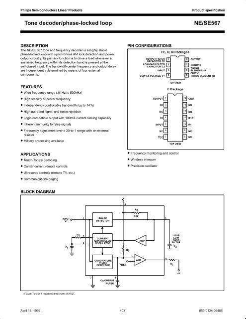
Philips Semiconductors Linear ProductsProduct specification<strong>Tone</strong> <strong>decoder</strong>/<strong>phase</strong>-<strong>locked</strong> <strong>loop</strong><strong>NE</strong>/<strong>SE567</strong>DESCRIPTIONThe <strong>NE</strong>/<strong>SE567</strong> tone and frequency <strong>decoder</strong> is a highly stable<strong>phase</strong>-<strong>locked</strong> <strong>loop</strong> with synchronous AM lock detection and poweroutput circuitry. Its primary function is to drive a load whenever asustained frequency within its detection band is present at theself-biased input. The bandwidth center frequency and output delayare independently determined by means of four externalcomponents.PIN CONFIGURATIONSOUTPUT FILTERCAPACITOR C3LOW-PASS FILTERCAPACITOR C2INPUTSUPPLY VOLTAGE V+FE, D, N Packages1238764 5OUTPUTGROUNDTIMINGELEMENTS R1AND C1TIMING ELEMENT R1FEATURES• Wide frequency range (.01Hz to 500kHz)• High stability of center frequency• Independently controllable bandwidth (up to 14%)• High out-band signal and noise rejection• Logic-compatible output with 100mA current sinking capability• Inherent immunity to false signals• Frequency adjustment over a 20-to-1 range with an externalresistor• Military processing availableAPPLICATIONS• Touch-<strong>Tone</strong>® decoding• Carrier current remote controls• Ultrasonic controls (remote TV, etc.)• Communications pagingOUTPUTC3NCC2INPUTNC123456TOP VIEWF Package1413121110V CC 7 8TOP VIEW• Frequency monitoring and control• Wireless intercom• Precision oscillator9GNDNCNCR1C1R1NCNCBLOCK DIAGRAM4R 2INPUTV13PHASEDETECTOR3.9k2C 1R 156CURRENTCONTROLLEDOSCILLATORR 3AMPLOOPLOWPASSFILTERC 2QUADRATUREPHASEDETECTORV REF+–AMP8R L7 1C 3 OUTPUTFILTER+V®Touch-<strong>Tone</strong> is a registered trademark of AT&T.April 15, 1992 403853-0124 06456
Philips Semiconductors Linear Products<strong>Tone</strong> <strong>decoder</strong>/<strong>phase</strong>-<strong>locked</strong> <strong>loop</strong>Product specification<strong>NE</strong>/<strong>SE567</strong>ORDERING INFORMATIONDESCRIPTION TEMPERATURE RANGE ORDER CODE DWG #8-Pin Plastic SO 0 to +70°C <strong>NE</strong>567D 0174C14-Pin Cerdip 0 to +70°C <strong>NE</strong>567F 0581B8-Pin Plastic DIP 0 to +70°C <strong>NE</strong>567N 0404B8-Pin Plastic SO -55°C to +125°C <strong>SE567</strong>D 0174C8-Pin Cerdip -55°C to +125°C <strong>SE567</strong>FE 0581B8-Pin Plastic DIP -55°C to +125°C <strong>SE567</strong>N 0404BABSOLUTE MAXIMUM RATINGST ASYMBOL PARAMETER RATING UNITOperating temperature<strong>NE</strong>567 0 to +70 °C<strong>SE567</strong> -55 to +125 °CV CC Operating voltage 10 VV+ Positive voltage at input 0.5 +V S VV- Negative voltage at input -10 V DCV OUT Output voltage (collector of output transistor) 15 V DCT STG Storage temperature range -65 to +150 °CP D Power dissipation 300 mWApril 15, 1992 405
Philips Semiconductors Linear Products<strong>Tone</strong> <strong>decoder</strong>/<strong>phase</strong>-<strong>locked</strong> <strong>loop</strong>Product specification<strong>NE</strong>/<strong>SE567</strong>DC ELECTRICAL CHARACTERISTICSV +=5.0V; T A =25°C, unless otherwise specified.SYM-BOLCenter frequency 1PARAMETER TEST CONDITIONS <strong>SE567</strong> <strong>NE</strong>567 UNITMin Typ Max Min Typ Maxf O Highest center frequency 500 500 kHzf O Center frequency stability 2 -55 to +125°C 35 ±140 35 ±140 ppm/°Cf OCenter frequency distributionf O0 to +70°C 35 ±60 35 ±60 ppm/°C 100kHz 1 -10 0 +10 -10 0 +10 %1.1R 1 C 1f OCenter frequency shift with supplyvoltageDetection bandwidthBWLargest detection bandwidthf Of O 100kHz 100kHz 10.5 1 0.7 2 %/V1.1R 1 C 11 12 14 16 10 14 18 % of f O1.1R 1 C 1BW Largest detection bandwidth skew 2 4 3 6 % of f OBW Largest detection bandwidth— V I =300mV RMS ±0.1 ±0.1 %/°Cvariation with temperatureBW Largest detection bandwidth— V I =300mV RMS ±2 ±2 %/VInputvariation with supply voltageR IN Input resistance 15 20 25 15 20 25 kΩV I Smallest detectable input voltage 4 I L =100mA, f I =f O 20 25 20 25 mV RMSOutputLargest no-output input voltage 4 I L =100mA, f I =f O 10 15 10 15 mV RMSGreatest simultaneous out-band +6 +6 dBsignal-to-in-band signal ratioMinimum input signal to wide-bandnoise ratioB n =140kHz -6 -6 dBFastest on-off cycling rate f O /20 f O /20“1” output leakage current V 8 =15V 0.01 25 0.01 25 µA“0” output voltage I L =30mA 0.2 0.4 0.2 0.4 VI L =100mA 0.6 1.0 0.6 1.0 Vt F Output fall time 3 R L =50Ω 30 30 nst R Output rise time 3 R L =50Ω 150 150 nsGeneralV CC Operating voltage range 4.75 9.0 4.75 9.0 VSupply current quiescent 6 8 7 10 mASupply current—activated R L =20kΩ 11 13 12 15 mAt PD Quiescent power dissipation 30 35 mWNOTES:1. Frequency determining resistor R 1 should be between 2 and 20kΩ2. Applicable over 4.75V to 5.75V. See graphs for more detailed information.3. Pin 8 to Pin 1 feedback R L network selected to eliminate pulsing during turn-on and turn-off.4. With R 2 =130kΩ from Pin 1 to V+. See Figure 1.April 15, 1992 406
Philips Semiconductors Linear Products<strong>Tone</strong> <strong>decoder</strong>/<strong>phase</strong>-<strong>locked</strong> <strong>loop</strong>Product specification<strong>NE</strong>/<strong>SE567</strong>TYPICAL PERFORMANCE CHARACTERISTICS300Bandwidth vs InputSignal Amplitude(Hz * F)µ15Largest Detection bandwidthvs Operating FrequencyDetection bandwidth as aFunction of C 2 and C 3INPUT VOLTAGE — mVrms2502001501005000 2 4 6 8 10 12 14 16BANDWIDTH — % OF f OOLARGEST BANDWIDTH — % OF f10500.1 1 10 100 1000CENTER FREQUENCY — kHz10 510 410 610 3C 320 2 4 6 8 10 12 14 16BANDWIDTH — % OF f OTypical Supply Current vsSupply VoltageGreatest Number of CyclesBefore OutputTypical Output Voltage vsTemperatureCUPPLY CURRENT — mA2520151050NO LOAD“ON” CURRENTQUIESCENTCURRENT4 5 6 7 8 9 10CYCLES1000500300100503010BANDWIDTH LIMITED BYEXTERNAL RESISTOR(MINIMUM C 2 )BANDWIDTHLIMITED BY (C 2 )1 5 10 50 100OUTPUT VOLTAGE PIN 8 — V1.00.90.8I L = 100mA0.70.60.50.40.3I L = 30mA0.20.10–75 –25 0 25 75 125SUPPLY VOLTAGE — VBANDWIDTH — % OF f OTEMPERATURE — °CTypical Frequency DriftWith Temperature(Mean and SD)Typical Frequency DriftWith Temperature(Mean and SD)Typical Frequency DriftWith Temperature(Mean and SD)1.51.0+V = 4.75V1.51.0+V = 5.75V5.52.5(2)+V = 7.0V (1)+V = 9.0V (2)0.50.50(1)00–2.5–0.5–0.5–5.0–1.0–1.0–7.5–1.5–75 –25 0 25 75 125–1.5–75 –25 0 25 75 125–10–75 –25 0 25 75 125TEMPERATURE — °C TEMPERATURE — °C TEMPERATURE — °CApril 15, 1992 407
Philips Semiconductors Linear Products<strong>Tone</strong> <strong>decoder</strong>/<strong>phase</strong>-<strong>locked</strong> <strong>loop</strong>Product specification<strong>NE</strong>/<strong>SE567</strong>TYPICAL PERFORMANCE CHARACTERISTICS (Continued)TEMPERATURE COEFFICIENT— ppm/ C°1000–100–200Center Frequency TemperatureCoefficient(Mean and SD)∆t = 0°C to 70°C–3004.5 5.0 5.5 6.0 6.5 7.0SUPPLY VOLTAGE — Vt Ot O V 1.00.90.80.70.6% V0.50.40.30.20.1Center FrequencyShift With SupplyVoltage Change vsOperating Frequency01 2 3 4 5 10 20 40 100CENTER FREQUENCY — kHzBANDWIDTH — % OF f O15.012.510.07.55.02.50Typical Bandwidth VariationTemperature1412108642BANDWIDTH AT 25°C–75 –25 0 25 75 125TEMPERATURE – °CDESIGN FORMULASf O 11.1R 1 C 1BW 1070V I V If O C 2200mV RMSin % of f OWhereV I =Input voltage (V RMS )C 2 =Low-pass filter capacitor (µF)PHASE-LOCKED LOOP TERMINOLOGY CENTERFREQUENCY (f O )The free-running frequency of the current controlled oscillator (CCO)in the absence of an input signal.Detection Bandwidth (BW)The frequency range, centered about f O , within which an input signalabove the threshold voltage (typically 20mV RMS ) will cause a logicalzero state on the output. The detection bandwidth corresponds tothe <strong>loop</strong> capture range.Lock RangeThe largest frequency range within which an input signal above thethreshold voltage will hold a logical zero state on the output.Detection Band SkewA measure of how well the detection band is centered about thecenter frequency, f O . The skew is defined as (f MAX +f MIN -2f O )/2f Owhere fmax and fmin are the frequencies corresponding to theedges of the detection band. The skew can be reduced to zero ifnecessary by means of an optional centering adjustment.OPERATING INSTRUCTIONSFigure 1 shows a typical connection diagram for the 567. For mostapplications, the following three-step procedure will be sufficient forchoosing the external components R 1 , C 1 , C 2 and C 3 .1. Select R1 and C1 for the desired center frequency. For besttemperature stability, R1 should be between 2K and 20K ohm,and the combined temperature coefficient of the R1C1 productshould have sufficient stability over the projected temperaturerange to meet the necessary requirements.2. Select the low-pass capacitor, C 2 , by referring to the Bandwidthversus Input Signal Amplitude graph. If the input amplitudeVariation is known, the appropriate value of f O ⋅ C 2 necessary togive the desired bandwidth may be found. Conversely, an area ofoperation may be selected on this graph and the input level andC2 may be adjusted accordingly. For example, constantbandwidth operation requires that input amplitude be above200mV RMS . The bandwidth, as noted on the graph, is thencontrolled solely by the f O ⋅ C 2 product (f O (Hz), C2(µF)).April 15, 1992 408
Philips Semiconductors Linear Products<strong>Tone</strong> <strong>decoder</strong>/<strong>phase</strong>-<strong>locked</strong> <strong>loop</strong>Product specification<strong>NE</strong>/<strong>SE567</strong>TYPICAL RESPONSEINPUTOUTPUTNOTE:R L = 100ΩResponse to 100mV RMS <strong>Tone</strong> Burstsaturates; its collector voltage being less than 1.0 volt (typically0.6V) at full output current (100mA). The voltage at Pin 2 is the<strong>phase</strong> detector output which is a linear function of frequency overthe range of 0.95 to 1.05 f O with a slope of about 20mV per percentof frequency deviation. The average voltage at Pin 1 is, during lock,a function of the in-band input amplitude in accordance with thetransfer characteristic given. Pin 5 is the controlled oscillator squarewave output of magnitude (+V -2V BE )≅(+V-1.4V) having a DCaverage of +V/2. A 1kΩ load may be driven from pin 5. Pin 6 is anexponential triangle of 1V P-P with an average DC level of +V/2. Onlyhigh impedance loads may beOUTPUTINPUTOUTPUT(PIN 8)7% 14% BWV CE (SAT) < 1.0VV+0NOTES:S/N = –6dBR L = 100ΩNoise Bandwidth = 140HzResponse to Same Input <strong>Tone</strong> BurstWith Wideband Noise3. The value of C3 is generally non-critical. C3 sets the band edgeof a low-pass filter which attenuates frequencies outside thedetection band to eliminate spurious outputs. If C3 is too small,frequencies just outside the detection band will switch the outputstage on and off at the beat frequency, or the output may pulseon and off during the turn-on transient. If C3 is too large, turn-onand turn-off of theINPUT 35+V +V4R LLOW PASSFILTER(PIN 2)PIN 1VOLTAGE(AVG)4.03.50.9f Of O1.1f OV REFTHRESHOLD VOLTAGE3.0f 1 = f O2.50 100 200mVrmsIN-BANDINPUTVOLTAGEFigure 2. Typical Output Response3.9V3.8V3.7Vf O 1R 1C 1R 1567 86 2 7 1R 2C 1C 2LOWPASSFILTERFigure 1.C 3OUTPUTFILTERoutput stage will be delayed until the voltage on C 3 passes thethreshold voltage. (Such delay may be desirable to avoid spuriousoutputs due to transient frequencies.) A typical minimum value forC 3 is 2C 2 .4. Optional resistor R2 sets the threshold for the largest “no output”input voltage. A value of 130kΩ is used to assure the tested limitof 10mV RMS min. This resistor can be referenced to ground forincreased sensitivity. The explanation can be found in the“optional controls” section which follows.AVAILABLE OUTPUTS (Figure 1)The primary output is the uncommitted output transistor collector,Pin 8. When an in-band input signal is present, this transistorApril 15, 1992 409
Philips Semiconductors Linear Products<strong>Tone</strong> <strong>decoder</strong>/<strong>phase</strong>-<strong>locked</strong> <strong>loop</strong>Product specification<strong>NE</strong>/<strong>SE567</strong>V+R567 1 567 1C 3C 3Rcause supply voltage fluctuations which could, for example, shift thedetection band of narrow-band systems sufficiently to causemomentary loss of lock. The result is a low-frequency oscillation intoand out of lock. Such effects can be prevented by supplying heavyload currents from a separate supply or increasing the supply filtercapacitor.DECREASESENSITIVITY567 1R A50kC 3R B2.5kR C1.0kINCREASESENSITIVITYSILICONDIODES FORTEMPERATURECOMPENSATION(OPTIONAL)Figure 3. Sensitivity Adjustconnected to pin 6 without affecting the CCO duty cycle ortemperature stability.V+DECREASESENSITIVITYINCREASESENSITIVITYSPEED OF OPERATIONMinimum lock-up time is related to the natural frequency of the <strong>loop</strong>.The lower it is, the longer becomes the turn-on transient. Thus,maximum operating speed is obtained when C 2 is at a minimum.When the signal is first applied, the <strong>phase</strong> may be such as to initiallydrive the controlled oscillator away from the incoming frequencyrather than toward it. Under this condition, which is of courseunpredictable, the lock-up transient is at its worst and the theoreticalminimum lock-up time is not achievable. We must simply wait for thetransient to die out.The following expressions give the values of C 2 and C 3 which allowhighest operating speeds for various band center frequencies. Theminimum rate at which digital information may be detected withoutinformation loss due to the turn-on transient or output chatter isabout 10 cycles per bit, corresponding to an information transfer rateof f O /10 baud.V+V+V+V+OPERATING PRECAUTIONSA brief review of the following precautions will help the user achievethe high level of performance of which the 567 is capable.1. Operation in the high input level mode (above 200mV) will freethe user from bandwidth variations due to changes in the in-bandsignal amplitude. The inputstage is now limiting, however, so that out-band signals or highnoise levels can cause an apparent bandwidth reduction as theinband signal is suppressed. Also, the limiting action will createin-band components from sub-harmonic signals, so the 567becomes sensitive to signals at f O /3, f O /5, etc.2. The 567 will lock onto signals near (2n+1) f O , and will give anoutput for signals near (4n+1) f O where n=0, 1, 2, etc. Thus,signals at 5f O and 9f O can cause an unwanted output. If suchsignals are anticipated, they should be attenuated beforereaching the 567 input.3. Maximum immunity from noise and out-band signals is affordedin the low input level (below 200mV RMS ) and reduced bandwidthoperating mode. However, decreased <strong>loop</strong> damping causes theworst-case lock-up time to increase, as shown by the GreatestNumber of Cycles Before Output vs Bandwidth graph.4. Due to the high switching speeds (20ns) associated with 567operation, care should be taken in lead routing. Lead lengthsshould be kept to a minimum. The power supply should beadequately bypassed close to the 567 with a 0.01µF or greatercapacitor; grounding paths should be carefully chosen to avoidground <strong>loop</strong>s and unwanted voltage variations. Another factorwhich must be considered is the effect of load energization onthe power supply. For example, an incandescent lamp typicallydraws 10 times rated current at turn-on. This can be somewhatgreater when the output stage is made less sensitive, rejection ofthird harmonics or in-band harmonics (of lower frequencysignals) is also improved.C 356718R f *10kR LC f*OPTIONAL - PERMITSLOWER VALUE OF C f56718C 3R A200 TO1kR LR f10k567Figure 4. Chatter Prevention567 2 567 2LOWERS f O567 1RAISES f OV+RC 2R A50kC 2V+RAISES f OR B2.5kR C1.0kFigure 5. Skew AdjustR A200 TO 1kR f1 10kC 28LOWERS f ORAISES f ORSILICONDIODES FORTEMPERATURECOMPENSATION(OPTIONAL)R LApril 15, 1992 410
Philips Semiconductors Linear Products<strong>Tone</strong> <strong>decoder</strong>/<strong>phase</strong>-<strong>locked</strong> <strong>loop</strong>Product specification<strong>NE</strong>/<strong>SE567</strong>C 2 130f OC 3 260f O F FIn cases where turn-off time can be sacrificed to achieve fastturn-on, the optional sensitivity adjustment circuit can be used tomove the quiescent C 3 voltage lower (closer to the thresholdvoltage). However, sensitivity to beat frequencies, noise andextraneous signals will be increased.OPTIONAL CONTROLS (Figure 3)The 567 has been designed so that, for most applications, noexternal adjustments are required. Certain applications, however,will be greatly facilitated if full advantage is taken of the addedcontrol possibilities available through the use of additional externalcomponents. In the diagrams given, typicalvalues are suggested where applicable. For best results theresistors used, except where noted, should have the sametemperature coefficient. Ideally, silicon diodes would below-resistivity types, such as forward-biased transistor base-emitterjunctions. However, ordinary low-voltage diodes should be adequatefor most applications.SENSITIVITY ADJUSTMENT (Figure 3)When operated as a very narrow-band detector (less than 8percent), both C 2 and C 3 are made quite large in order to improvenoise and out-band signal rejection. This will inevitably slow theresponse time. If, however, the output stage is biased closer to thethreshold level, the turn-on time can beimproved. This is accomplished by drawing additional current toterminal 1. Under this condition, the 567 will also give an output forlower-level signals (10mV or lower).By adding current to terminal 1, the output stage is biased furtheraway from the threshold voltage. This is most useful when, to obtainmaximum operating speed, C 2 and C 3 are made very small.Normally, frequencies just outside the detection band could causefalse outputs under this condition. By desensitizing the output stage,the out-band beat notes do not feed through to the output stage.Since the input level mustR A10kV+567 81V+R LINPUT VOLTAGE MV — RMS2500.5k 0.9k 1.4k 1.9k 2.5k 3.2k 4.0k20015010k20k100100k50R0 0 2 4 6 8 10 12 14 16UNLATCHUNLATCHV+C AC 3567 81R f20kR f20kC 3V+R LDETECTION BAND — % OF f OV+NOTE:C A prevents latch-up when power supply is turned on.PIN 2567R A50kR BR R AR BR BR CR CFigure 7. Output LatchingC 2R COPTIONAL SILICONDIODES FORTEMPERATURECOMPENSATIONNOTE:130 10k R Cf R 2O1300 10k Rf R OAdjust control for symmetry of detection band edgesabout f O .Figure 6. BW ReductionApril 15, 1992 411
Philips Semiconductors Linear Products<strong>Tone</strong> <strong>decoder</strong>/<strong>phase</strong>-<strong>locked</strong> <strong>loop</strong>Product specification<strong>NE</strong>/<strong>SE567</strong>CHATTER PREVENTION (Figure 4)Chatter occurs in the output stage when C 3 is relatively small, sothat the lock transient and the AC components at the quadrature<strong>phase</strong> detector (lock detector) output cause the output stage tomove through its threshold more than once. Many loads, forexample lamps and relays, will not respond to the chatter. However,logic may recognize the chatter as a series of outputs. By feedingthe output stage output back to its input (Pin 1) the chatter can beeliminated. Three schemes for doing this are given in Figure 4. Alloperate by feeding the first output step (either on or off) back to theinput, pushing the input past the threshold until the transientconditions are over. It is only necessary to assure that the feedbacktime constant is not so large as to prevent operation at the highestanticipated speed. Although chatter can always be eliminated bymaking C 3 large, the feedback circuit will enable faster operation ofthe 567 by allowing C 3 to be kept small. Note that if the feedbacktime constant is made quite large, a short burst at the inputfrequency can be stretched into a long output pulse. This may beuseful to drive, for example, stepping relays.DETECTION BAND CENTERING (OR SKEW)ADJUSTMENT (Figure 5)When it is desired to alter the location of the detection band(corresponding to the <strong>loop</strong> capture range) within the lock range, thecircuits shown above can be used. By moving the detection band toone edge of the range, for example, input signal variations willexpand the detection band in only one direction. This may proveuseful when a strong but undesirable signal is expected on one sideor the other of the center frequency. Since R B also alters the dutycycle slightly, this method may be used to obtain a precise dutycycle when the 567 is used as an oscillator.ALTERNATE METHOD OF BANDWIDTHREDUCTION (Figure 6)Although a large value of C 2 will reduce the bandwidth, it alsoreduces the <strong>loop</strong> damping so as to slow the circuit response time.This may be undesirable. Bandwidth can be reduced by reducingthe <strong>loop</strong> gain. This scheme will improve damping and permit fasteroperation under narrow-band conditions. Note that the reducedimpedance level at terminal 2 will require that a larger value of C 2 beused for a given filter cutofffrequency. If more than three 567s are to be used, the network of R Band R C can be eliminated and the R A resistors connected together.A capacitor between this junction and ground may be required toshunt high frequency components.OUTPUT LATCHING (Figure 7)To latch the output on after a signal is received, it is necessary toprovide a feedback resistor around the output stage (between Pins 8and 1). Pin 1 is pulled up to unlatch the output stage.REDUCTION OF C1 VALUEFor precision very low-frequency applications, where the value of C 1becomes large, an overall cost savings may be achieved byinserting a voltage-follower between the R 1 C 1 junction and Pin 6,so as to allow a higher value of R 1 and a lower value of C 1 for agiven frequency.PROGRAMMINGTo change the center frequency, the value of R 1 can be changedwith a mechanical or solid state switch, or additional C 1 capacitorsmay be added by grounding them through saturating NPNtransistors.April 15, 1992 412
Philips Semiconductors Linear Products<strong>Tone</strong> <strong>decoder</strong>/<strong>phase</strong>-<strong>locked</strong> <strong>loop</strong>Product specification<strong>NE</strong>/<strong>SE567</strong>TYPICAL APPLICATIONS+R 1C 1567897Hz567770HzC 3R 3R 2+C 21234567852Hz567941Hz++5678905671209Hz+*NOTES:Component values (Typical)R 1 = 26.8 to 15kΩR 2 = 24.7kΩR 3 = 20kΩC 1 = 0.10mFDIGITC 2 = 1.0mF 5VC 3 = 2.2mF 6VC 4 = 250µF 6V5671336Hz5671477Hz++Touch-<strong>Tone</strong> ® DecoderApril 15, 1992 413
Philips Semiconductors Linear Products<strong>Tone</strong> <strong>decoder</strong>/<strong>phase</strong>-<strong>locked</strong> <strong>loop</strong>Product specification<strong>NE</strong>/<strong>SE567</strong>TYPICAL APPLICATIONS (Continued)+5 TO 15V60Hz AC LI<strong>NE</strong>500pF50–200V RMSC 427pF3 567 85 6 2 1K 1LOADR 1–++565671:1R 12.5kΩC 15741f O ≈ 100kHz C 2C .00610.004mfdC 3.02AUDIO OUT(IF INPUT ISFREQUENCYMODULATED)Precision VLF+VCarrier-Current Remote Control or Intercom356785 6 2 1+V20kINPUT SIGNAL(>100mVrms)R 1C 2f 13 567 85 6 2 1C 1C 3R LR 1INPUTCHAN<strong>NE</strong>LOR RECEIVERC 1 C 2 C 3+VNORV O35675 6 2 18f 23 567 85 6 2 120kR’ 1C’ 1C’ 2C2 C 2 130f O(mfd)C1 C 1R1 1.12R 1R’ 124% Bandwidth <strong>Tone</strong> DecoderC’ 1 C’ 2 C’ 3Dual-<strong>Tone</strong> Decoder100mv (pp)SQUARE OR50mVRMSSI<strong>NE</strong> INPUT567 3 526R 1f 2OUTPUT(INTO 1kOHM MIN.LOAD)+90°PHASESHIFTC 2C 1NOTES:R 2 = R 1 /5Adjust R 1 so that φ = 90° with control midway.NOTES:1. Resistor and capacitor values chosen for desired frequencies and bandwidth.2. If C3 is made large so as to delay turn-on of the top 567, decoding of sequential (f 1 f 2 ) tones is possible.0° to 180° Phase ShifterApril 15, 1992 414
Philips Semiconductors Linear Products<strong>Tone</strong> <strong>decoder</strong>/<strong>phase</strong>-<strong>locked</strong> <strong>loop</strong>Product specification<strong>NE</strong>/<strong>SE567</strong>TYPICAL APPLICATIONS (Continued)++R LR L5673CON<strong>NE</strong>CT PIN 3TO 2.8V TOINVERT OUTPUT5672 6 5880°5672 6 538f OVCOTERMINAL(±6%)2 6 5R 1R L > 1000ΩR 1R L > 1000ΩR 110kC 2C 1C LC 2C 1Oscillator With Quadrature OutputOscillator With Double FrequencyOutputPrecision Oscillator With 20nsSwitching++567R L6 55678R LOUTPUT3 6 5110kΩVCOTERMINAL(±6%)5672 6 518R 1100kΩ1kΩ (MIN)R 1C 1C 2C 1C 1DUTYCYCLEADJUSTPulse Generator With 25% Duty CyclePrecision Oscillator to Switch 100mALoadsPulse GeneratorApril 15, 1992 415
This datasheet has been download from:www.datasheetcatalog.comDatasheets for electronics components.