EM260 ZigBee/802.15.4 Network Processor - 120-0260 ... - wless.ru
EM260 ZigBee/802.15.4 Network Processor - 120-0260 ... - wless.ru
EM260 ZigBee/802.15.4 Network Processor - 120-0260 ... - wless.ru
You also want an ePaper? Increase the reach of your titles
YUMPU automatically turns print PDFs into web optimized ePapers that Google loves.
INSPIRE GK12 Lesson PlanLesson TitleDensity ExperimentsLength of Lesson1 dayCreated ByKimberley LeggettSubjectScienceGrade Level10 th , 11 th , 12 th (Chemistry)State StandardsChemistry: 1c, e, g; 2aDOK Level DOK 3DOK ApplicationCompare; formulate; critique; hypothesize; drawconclusionsNational Standards9-12: A: Science as Inquiry; B: Physical Science;E: Science and Technology; G: History andNature of ScienceGraduate Research Element Density is a property of matter; properties ofmatter are relevant to my everyday researchStudent Learning Goal:Inquiry: 1. Apply inquiry-based and problem-solving processes and skills to scientificinvestigations: (c) Demonstrate the use of scientific inquiry and methods to formulate,conduct, and evaluate laboratory investigations (e.g., hypotheses, experimental design,observations, data analyses, interpretations, theory development); (e) evaluateprocedures, data, and conclusions to critique the scientific validity of research; (g)collect, analyze, and draw conclusions from data to create a formal presentation usingavailable technology (e.g., calculators)Physical Science: 2. Demonstrate an understanding of the atomic model of matter byexplaining atomic st<strong>ru</strong>cture and chemical bonding: (a) describe and classify matter basedon physical and chemical properties and interactions between molecules of atoms.Physical properties (e.g.; densities) of a variety of substancesNational Science Education Standards of Content 9-12A: Science as Inquiry: Use technology and mathematics to improve investigationsand communications:A variety of technologies, such as hand tools, measuring inst<strong>ru</strong>ments, andcalculators, should be an integral component of scientific investigations.Mathematics plays an essential role in all aspects of an inquiry. For example,measurement is used for posing questions, formulas are used for developingexplanations, and charts and graphs are used for communicating results.B: st<strong>ru</strong>cture and properties of matterE: implement a proposed solution; evaluate the solution and its consequences;communicate the problem, process, and solutionG: historical perspectivesINSPIRE Project Funded by the NSF Graduate K-12 Program 1
<strong>EM260</strong>General DescriptionNote: Ember has moved several important sections into standalone documents. Section 6 describing theASH protocol has been moved to the UART Gateway Protocol Reference (<strong>120</strong>-3010-000). Section 7on EZSP has been moved to the EZSP Reference Guide (<strong>120</strong>-3009-000).The <strong>EM260</strong> integrates a 2.4GHz, IEEE <strong>802.15.4</strong>-compliant transceiver with a 16-bit network processor (XAP2bcore) to <strong>ru</strong>n EmberZNet, the Ember <strong>ZigBee</strong>-compliant network stack. The <strong>EM260</strong> exposes access to theEmberZNet API across a standard SPI module or a UART module, allowing application development on a Hostplatform. This means that the <strong>EM260</strong> can be viewed as a <strong>ZigBee</strong> peripheral connected over a serial interface.The XAP2b microprocessor is a power-optimized core integrated in the <strong>EM260</strong>. It contains integrated Flash andRAM memory along with an optimized peripheral set to enhance the operation of the network stack.The transceiver utilizes an efficient architecture that exceeds the dynamic range requirements imposed bythe IEEE <strong>802.15.4</strong>-2003 standard by over 15dB. The integrated receive channel filtering allows for co-existencewith other communication standards in the 2.4GHz spect<strong>ru</strong>m such as IEEE 802.11g and Bluetooth. Theintegrated regulator, VCO, loop filter, and power amplifier keep the external component count low. Anoptional high-performance radio mode (boost mode) is software selectable to boost dynamic range by afurther 3dB.The <strong>EM260</strong> contains embedded Flash and integrated RAM for program and data storage. By employing aneffective wear-leveling algorithm, the stack optimizes the lifetime of the embedded Flash, and affords theapplication the ability to configure stack and application tokens within the <strong>EM260</strong>.To maintain the strict timing requirements imposed by <strong>ZigBee</strong> and the IEEE <strong>802.15.4</strong>-2003 standard, the <strong>EM260</strong>integrates a number of MAC functions into the hardware. The MAC hardware handles automatic ACKtransmission and reception, automatic backoff delay, and clear channel assessment for transmission, as wellas automatic filtering of received packets. In addition, the <strong>EM260</strong> allows for t<strong>ru</strong>e MAC level debugging byintegrating the Packet Trace Interface.An integrated voltage regulator, power-on-reset circuitry, sleep timer, and low-power sleep modes areavailable. The deep sleep and power down modes draw less than 1μA, allowing products to achieve longbattery life.Finally, the <strong>EM260</strong> utilizes the non-int<strong>ru</strong>sive SIF module for powerful software debugging and programming ofthe network processor.Target applications for the <strong>EM260</strong> include:• Building automation and control• Home automation and control• Home entertainment control• Asset trackingThe <strong>EM260</strong> can only be purchased with the EmberZNet stack. This technical datasheet details the <strong>EM260</strong>features available to customers using it with the EmberZNet stack.<strong>120</strong>-<strong>0260</strong>-000J Page 2
<strong>EM260</strong>1 Pin AssignmentsVDD_24MHZOSCAOSCBVDD_SYNTH_PREVDD_COREnWAKELINK_ACTIVITYSDBGVDD_FLASHGND40 39 38 37 36 35 34 33 32 31VDD_VCORF_P1241GND3029nSIF_LOADSIF_MOSIRF_N328SIF_MISOVDD_RFRF_TX_ALT_PRF_TX_ALT_N456<strong>EM260</strong>272625SIF_CLKnHOST_INTN.C.VDD_IF724VDD_PADSBIAS_R823PTI_DATAVDD_PADSA922PTI_ENTX_ACTIVE1021nSSEL11 12 13 14 15 16 17 18 19 20nRESETVREG_OUTVDD_PADSVDD_COREnSSEL_INTN.C.MOSIMISOVDD_PADSSCLKFigure 1. <strong>EM260</strong> Pin Assignment for SPI ProtocolVDD_24MHZOSCAOSCBVDD_SYNTH_PREVDD_COREN.C.LINK_ACTIVITYSDBGVDD_FLASHGND40 39 38 37 36 35 34 33 32 31VDD_VCORF_P1241GND3029nSIF_LOADSIF_MOSIRF_N328SIF_MISOVDD_RFRF_TX_ALT_PRF_TX_ALT_N456<strong>EM260</strong>272625SIF_CLKRXDTXDVDD_IF724VDD_PADSBIAS_R823PTI_DATAVDD_PADSA922PTI_ENTX_ACTIVE1021N.C.11 12 13 14 15 16 17 18 19 20nRESETVREG_OUTVDD_PADSV DD_COREnCTSnRTSN.C.N.C.VDD_PADSN.C.Figure 2. <strong>EM260</strong> Pin Assignment for UART Protocol<strong>120</strong>-<strong>0260</strong>-000J Page 4
<strong>EM260</strong>Table 1. Pin DescriptionsPin # Signal DirectionDescription1 VDD_VCO Power 1.8V VCO supply; should be connected to VREG_OUT2 RF_P I/O Differential (with RF_N) receiver input/transmitter output3 RF_N I/O Differential (with RF_P) receiver input/transmitter output4 VDD_RF Power 1.8V RF supply (LNA and PA); should be connected to VREG_OUT5 RF_TX_ALT_P O Differential (with RF_TX_ALT_N) transmitter output (optional)6 RF_TX_ALT_N O Differential (with RF_TX_ALT_P) transmitter output (optional)7 VDD_IF Power 1.8V IF supply (mixers and filters); should be connected to VREG_OUT8 BIAS_R I Bias setting resistor9 VDD_PADSA Power Analog pad supply (1.8V); should be connected to VREG_OUT10 TX_ACTIVE O Logic-level control for external RX/TX switch11 nRESET I Active low chip reset (internal pull-up)12 VREG_OUT Power Regulator output (1.8V)13 VDD_PADS Power Pads supply (2.1 – 3.6V)The <strong>EM260</strong> baseband controls TX_ACTIVE and drives it high (1.8V) when in TX mode.(Refer to Table 6 and section 4.2.2.)14 VDD_CORE Power 1.8V digital core supply; should be connected to VREG_OUT15nSSEL_INT I SPI Slave Select Inter<strong>ru</strong>pt (from Host to <strong>EM260</strong>)When using the SPI interface, this signal must be connected to nSSEL (Pin 21)nCTS I UART Clear To Send (enables <strong>EM260</strong> transmission)When using the UART interface, this signal should be left unconnected if not used.16N.C. I When using the SPI interface, this signal is left not connected.nRTS O UART Request To Send (enables Host transmission)When using the UART interface, this signal should be left unconnected if not used.17MOSI I SPI Data, Master Out / Slave In (from Host to <strong>EM260</strong>)N.C. I When using the UART interface, this signal is left not connected.18MISO O SPI Data, Master In / Slave Out (from <strong>EM260</strong> to Host)N.C. I When using the UART interface, this signal is left not connected.19 VDD_PADS Power Pads supply (2.1 – 3.6V)20SCLK I SPI Clock (from Host to <strong>EM260</strong>)N.C. I When using the UART interface, this signal is left not connected.21nSSEL I SPI Slave Select (from Host to <strong>EM260</strong>)N.C. I When using the UART interface, this signal is left not connected.22 PTI_EN O Frame signal of Packet Trace Interface (PTI)23 PTI_DATA O Data signal of Packet Trace Interface (PTI)Page 5<strong>120</strong>-<strong>0260</strong>-000J
<strong>EM260</strong>Pin # Signal DirectionDescription24 VDD_PADS Power Pads supply (2.1 – 3.6V)25N.C. I When using the SPI interface, this signal is left not connected.TXD O UART Transmitted Data (from <strong>EM260</strong> to Host)26nHOST_INT O SPI Host Inter<strong>ru</strong>pt signal (from <strong>EM260</strong> to Host)RXD I UART Received Data (from Host to <strong>EM260</strong>)27 SIF_CLK I Programming and Debug Interface, Clock (internal pull down)28 SIF_MISO O Programming and Debug Interface, Master In / Slave Out29 SIF_MOSI I Programming and Debug Interface, Master Out / Slave In (external pull-down requiredto guarantee state in Deep Sleep Mode)30 nSIF_LOAD I/O Programming and Debug Interface, load strobe (open collector with internal pull up)31 GND Power Ground Supply32 VDD_FLASH Power 1.8V Flash memory supply; should be connected to VREG_OUT33 SDBG O Spare Debug signal34 LINK_ACTIVITY O Link and Activity signal35nWAKE I SPI Wake Inter<strong>ru</strong>pt signal (from Host to <strong>EM260</strong>)N.C. I When using the UART interface, this signal is left not connected.36 VDD_CORE Power 1.8V digital core supply; should be connected to VREG_OUT37 VDD_SYNTH_PRE Power 1.8V synthesizer and prescalar supply; should be connected to VREG_OUT38 OSCB I/O 24MHz crystal oscillator or left open for when using an external clock input on OSCA39 OSCA I/O 24MHz crystal oscillator or external clock input40 VDD_24MHZ Power 1.8V high-frequency oscillator supply; should be connected to VREG_OUT41 GND Ground Ground supply pad in the bottom center of the package forms Pin 41 (see the <strong>EM260</strong>Reference Design for PCB considerations)<strong>120</strong>-<strong>0260</strong>-000J Page 6
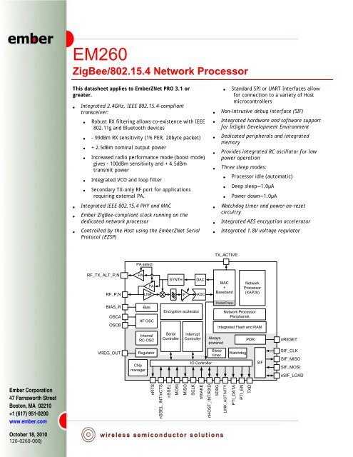
<strong>EM260</strong>2 Top-Level Functional DescriptionFigure 3 shows a detailed block diagram of the <strong>EM260</strong>.TX_ACTIVEPA selectRF_TX_ALT_P,NRF_P,NPAPALNASYNTHIFDACADCMAC+Baseband<strong>Network</strong><strong>Processor</strong>(XAP2b)BIAS_ROSCAOSCBBiasHF OSCEncryption accleratorPacketTrace<strong>Network</strong> <strong>Processor</strong>PeripheralsIntegrated Flash and RAMInternalRC-OSCSerialControllerInter<strong>ru</strong>ptControllerAlwayspoweredPORnRESETVREG_OUTRegulatorChipmanagerIO ControllerSleeptimerWatchdogSIFSIF_CLKSIF_MISOSIF_MOSInSIF_LOADnRTSnSSEL_INT/nCTSnSSELMOSIMISOSCLKnWAKEnHOST_INT/RXDSDBGLINK_ACTIVITYPTI_DATAPTI_ENTXDFigure 3. <strong>EM260</strong> Block DiagramThe radio receiver is a low-IF, super-heterodyne receiver. It utilizes differential signal paths to minimize noiseinterference, and its architecture has been chosen to optimize co-existence with other devices within the2.4GHz band (namely, IEEE 802.11g and Bluetooth). After amplification and mixing, the signal is filtered andcombined prior to being sampled by an ADC.The digital receiver implements a coherent demodulator to generate a chip stream for the hardware-basedMAC. In addition, the digital receiver contains the analog radio calibration routines and control of the gainwithin the receiver path.The radio transmitter utilizes an efficient architecture in which the data stream directly modulates the VCO.An integrated PA boosts the output power. The calibration of the TX path as well as the output power iscontrolled by digital logic. If the <strong>EM260</strong> is to be used with an external PA, the TX_ACTIVE signal should be usedto control the timing of the external switching logic.The integrated 4.8 GHz VCO and loop filter minimize off-chip circuitry. Only a 24MHz crystal with its loadingcapacitors is required to properly establish the PLL reference signal.Page 7<strong>120</strong>-<strong>0260</strong>-000J
<strong>EM260</strong>The MAC interfaces the data memory to the RX and TX baseband modules. The MAC provides hardware-basedIEEE <strong>802.15.4</strong> packet-level filtering. It supplies an accurate symbol time base that minimizes thesynchronization effort of the software stack and meets the protocol timing requirements. In addition, itprovides timer and synchronization assistance for the IEEE <strong>802.15.4</strong> CSMA-CA algorithm.The <strong>EM260</strong> integrates hardware support for a Packet Trace module, which allows robust packet-based debug.This element is a critical component of InSight Desktop, the Ember software IDE, providing advanced networkdebug capability when coupled with the InSight Adapter.The <strong>EM260</strong> integrates a 16-bit XAP2b microprocessor developed by Cambridge Consultants Ltd. This powerefficient,industry-proven core provides the appropriate level of processing power to meet the needs of theEmber <strong>ZigBee</strong>-compliant stack, EmberZNet. In addition, the SIF module provides a non-int<strong>ru</strong>sive programmingand debug interface allowing for real-time application debugging.The <strong>EM260</strong> exposes the Ember Serial API over either a SPI or UART interface, which allows applicationdevelopment to occur on a Host platform of choice. The SPI interface uses the four standard SPI signals plustwo additional signals, nHOST_INT and nWAKE, which provide an easy-to-use handshake mechanism betweenthe Host and the <strong>EM260</strong>. The UART interface uses the two standard UART signals and also supports eitherstandard RTS/CTS or XON/XOFF flow control.The integrated voltage regulator generates a regulated 1.8V reference voltage from an unregulated supplyvoltage. This voltage is decoupled and routed externally to supply the 1.8V to the core logic. In addition, anintegrated POR module allows for the proper cold start of the <strong>EM260</strong>.The <strong>EM260</strong> contains one high-frequency (24MHz) crystal oscillator and, for low-power operation, a second lowfrequencyinternal 10 kHz oscillator.The <strong>EM260</strong> contains two power domains. The always-powered High Voltage Supply is used for powering theGPIO pads and critical chip functions. The rest of the chip is powered by a regulated Low Voltage Supply whichcan be disabled during deep sleep to reduce the power consumption.<strong>120</strong>-<strong>0260</strong>-000J Page 8
<strong>EM260</strong>3 Electrical Characteristics3.1 Absolute Maximum RatingsTable 2 lists the absolute maximum ratings for the <strong>EM260</strong>.Table 2. Absolute Maximum RatingsParameter Test Conditions Min. Max. UnitRegulator voltage (VDD_PADS) - 0.3 3.6 VCore voltage (VDD_24MHZ, VDD_VCO,VDD_RF, VDD_IF, VDD_PADSA, VDD_FLASH,VDD_SYNTH_PRE, VDD_CORE)- 0.3 2.0 VVoltage on RF_P,N; RF_TX_ALT_P,N - 0.3 3.6 VRF input power(for max level for correct packet reception,see Table 7)Voltage on nSSEL_INT, MOSI, MISO, SCLK,nSSEL, PTI_EN, PTI_DATA, nHOST_INT,SIF_CLK, SIF_MISO, SIF_MOSI, nSIF_LOAD,SDBG, LINK_ACTIVITY, nWAKE, nRESET,VREG_OUT+15 dBm- 0.3 VDD_PADS+0.3 VVoltage on TX_ACTIVE, BIAS_R, OSCA, OSCB - 0.3 VDD_CORE+0.3 VStorage temperature - 40 + 140 °C3.2 Recommended Operating ConditionsTable 3 lists the rated operating conditions of the <strong>EM260</strong>.Table 3. Operating ConditionsParameter Test Conditions Min. Typ. Max. UnitRegulator input voltage (VDD_PADS) 2.1 3.6 VCore input voltage (VDD_24MHZ, VDD_VCO,VDD_RF, VDD_IF, VDD_PADSA, VDD_FLASH,VDD_SYNTH_PRE, VDD_CORE)1.7 1.8 1.9 VTemperature range - 40 + 85 °CPage 9<strong>120</strong>-<strong>0260</strong>-000J
<strong>EM260</strong>3.3 Environmental CharacteristicsTable 4 lists the environmental characteristics of the <strong>EM260</strong>.Table 4. Environmental CharacteristicsParameter Test Conditions Min. Typ. Max. UnitESD (human body model) On any Pin - 2 + 2 kVESD (charged device model) Non-RF Pins -400ESD (charged device model) RF Pins -225+400+225VVMoisture Sensitivity Level (MSL)MSL3<strong>120</strong>-<strong>0260</strong>-000J Page 10
<strong>EM260</strong>3.4 DC Electrical CharacteristicsTable 5 lists the DC electrical characteristics of the <strong>EM260</strong>.Note: Current measurements were collected using the EmberZNet software stack Version 3.0.1.Table 5. DC CharacteristicsParameter Test Conditions Min. Typ. Max. UnitRegulator input voltage (VDD_PADS) 2.1 3.6 VPower supply range (VDD_CORE) 1.7 1.8 1.9 VDeep Sleep CurrentQuiescent current, including internalRC oscillatorAt 25° C 1.0 μARESET CurrentQuiescent current, nRESET assertedRX CurrentRadio receiver, MAC, and baseband(boost mode)Typ at 25° C/3VMax at 85° C/3.6V1.5 2.0 mA30.0 mARadio receiver, MAC, and baseband 28.0 mACPU, RAM, and Flash memory At 25° C and 1.8V core 8.0 mATotal RX current( = I Radio receiver, MAC and baseband, CPU +I RAM, and Flash memory )At 25° C, VDD_PADS = 3.0V 36.0 mATX CurrentRadio transmitter, MAC, and baseband(boost mode)Radio transmitter, MAC, and basebandAt max. TX power (+ 5dBmtypical)At max. TX power (+ 3dBmtypical)34.0 mA28.0 mAAt 0 dBm typical 24.0 mAAt min. TX power (- 32dBmtypical)19.0 mACPU, RAM, and Flash memory At 25° C, VDD_PADS = 3.0V 8.0 mATotal TX current( = I Radio transmitter, MAC and baseband, CPU +I RAM, and Flash memory )At 25° C and 1.8V core; max.power out36.0 mAPage 11<strong>120</strong>-<strong>0260</strong>-000J
<strong>EM260</strong>3.5 Digital I/O SpecificationsTable 6 contains the digital I/O specifications for the <strong>EM260</strong>. The digital I/O power (named VDD_PADS) comesfrom three dedicated pins (pins 13, 19, and 24). The voltage applied to these pins sets the I/O voltage.Table 6. Digital I/O SpecificationsParameter Name Min. Typ. Max. UnitVoltage supply VDD_PADS 2.1 3.6 VInput voltage for logic 0 V IL 0 0.2 xVDD_PADSVInput voltage for logic 1 V IH 0.8 x VDD_PADS VDD_PADS VInput current for logic 0 I IL -0.5 μAInput current for logic 1 I IH 0.5 μAInput pull-up resistor value R IPU 30 kΩInput pull-down resistor value R IPD 30 kΩOutput voltage for logic 0 V OL 0 0.18 xVDD_PADSVOutput voltage for logic 1 V OH 0.82 xVDD_PADSVDD_PADSVOutput source current (standardcurrent pad)Output sink current (standardcurrent pad)Output source current (high currentpad: pins 33, 34, and 35)Output sink current (high currentpad: pins 33, 34, and 35)I OHS 4 mAI OLS 4 mAI OHH 8 mAI OLH 8 mATotal output current (for I/O pads) I OH + I OL 40 mAInput voltage threshold for OSCA0.2 xVDD_CORE0.8 xVDD_PADSVOutput voltage level (TX_ACTIVE)0.18 xVDD_CORE0.82 xVDD_COREVOutput source current (TX_ACTIVE) 1 mA<strong>120</strong>-<strong>0260</strong>-000J Page 12
<strong>EM260</strong>3.6 RF Electrical Characteristics3.6.1 ReceiveTable 7 lists the key parameters of the integrated IEEE <strong>802.15.4</strong> receiver on the <strong>EM260</strong>.Note: Receive Measurements were collected with Ember’s <strong>EM260</strong> Ceramic Balun Reference Design at 2440MHzand using the EmberZNet software stack Version 3.0.1. The Typical number indicates one standard deviationabove the mean, measured at room temperature (25C). The Min and Max numbers are measured over processcorners at room temperature (25C).Note: The adjacent channel rejection (ACR) measurements were performed by using an unfiltered, ideal IEEE<strong>802.15.4</strong> signal of continuous pseudo-random data as the interferer. For more information on ACRmeasurement techniques, see Adjacent Channel Rejection Measurements (<strong>120</strong>-5059-000).Table 7. Receive CharacteristicsParameter Test Conditions Min. Typ. Max. UnitFrequency range 2400 2500 MHzSensitivity (boost mode)1% PER, 20byte packet defined byIEEE <strong>802.15.4</strong>-100- 95 dBmSensitivity1% PER, 20byte packet defined byIEEE <strong>802.15.4</strong>- 99 - 94 dBmHigh-side ACR IEEE <strong>802.15.4</strong> signal at -82dBm 35 dBLow-side ACR IEEE <strong>802.15.4</strong> signal at - 82dBm 35 dB2 nd high-side ACR IEEE <strong>802.15.4</strong> signal at - 82dBm 40 dB2 nd low-side ACR IEEE <strong>802.15.4</strong> signal at - 82dBm 40 dBChannel rejection for all otherchannels802.11g rejection centered at +12MHz or - 13MHzMaximum input signal level forcorrect operation (low gain)IEEE <strong>802.15.4</strong> signal at - 82dBm 40 dBIEEE <strong>802.15.4</strong> signal at - 82dBm 35 dB0 dBmImage suppression 30 dBCo-channel rejection IEEE <strong>802.15.4</strong> signal at - 82dBm - 6 dBcRelative frequency error(2 x 40 ppm required by IEEE<strong>802.15.4</strong>)-<strong>120</strong>+<strong>120</strong>ppmRelative timing error(2 x 40 ppm required by IEEE<strong>802.15.4</strong>)-<strong>120</strong>+<strong>120</strong>ppmLinear RSSI range 40 dBRSSI Range - 90 - 30 dBPage 13<strong>120</strong>-<strong>0260</strong>-000J
<strong>EM260</strong>3.6.2 TransmitTable 8 lists the key parameters of the integrated IEEE <strong>802.15.4</strong> transmitter on the <strong>EM260</strong>.Note: Transmit Measurements were collected with Ember’s <strong>EM260</strong> Ceramic Balun Reference Design at2440MHz and using the EmberZNet software stack Version 3.0.1. The Typical number indicates one standarddeviation below the mean, measured at room temperature (25C). The Min and Max numbers are measuredover process corners at room temperature (25C).Table 8. Transmit CharacteristicsParameter Test Conditions Min. Typ. Max. UnitMaximum output power (boostmode)At highest power setting 4.5 dBmMaximum output power At highest power setting -0.52.5 dBmMinimum output power At lowest power setting - 32 dBmError vector magnitude As defined by IEEE <strong>802.15.4</strong>,which sets a 35% maximum15 25 %Carrier frequency error - 40 + 40 ppmLoad impedance 200 ΩPSD mask relative 3.5MHz away - 20 dBPSD mask absolute 3.5MHz away - 30 dBm3.6.3 SynthesizerTable 9 lists the key parameters of the integrated synthesizer on the <strong>EM260</strong>.Table 9. Synthesizer CharacteristicsParameter Test Conditions Min. Typ. Max. UnitFrequency range 2400 2500 MHzFrequency resolution 11.7 kHzLock time From off, with correct VCO DAC setting 100 μsRelock timeChannel change or RX/TX turnaround(IEEE <strong>802.15.4</strong> defines 192μs turnaroundtime)100 μsPhase noise at 100kHz - 71 dBc/HzPhase noise at 1MHz - 91 dBc/HzPhase noise at 4MHz -103Phase noise at 10MHz -111dBc/HzdBc/Hz<strong>120</strong>-<strong>0260</strong>-000J Page 14
<strong>EM260</strong>4 Functional DescriptionThe <strong>EM260</strong> connects to the Host platform through either a standard SPI interface or a standard UARTinterface. The EmberZNet Serial Protocol (EZSP) has been defined to allow an application to be written on ahost platform of choice. Therefore, the <strong>EM260</strong> comes with a license to EmberZNet, the Ember <strong>ZigBee</strong>compliantsoftware stack. The following brief description of the hardware modules provides the necessarybackground on the operation of the <strong>EM260</strong>. For more information, contact www.ember.com/support.4.1 Receive (RX) PathThe <strong>EM260</strong> RX path spans the analog and digital domains. The RX architecture is based on a low-IF, superheterodynereceiver. It utilizes differential signal paths to minimize noise interference. The input RF signal ismixed down to the IF frequency of 4MHz by I and Q mixers. The output of the mixers is filtered and combinedprior to being sampled by a 12Msps ADC. The RX filtering within the RX path has been designed to optimize theco-existence of the <strong>EM260</strong> with other 2.4GHz transceivers, such as the IEEE 802.11g and Bluetooth.4.1.1 RX BasebandThe <strong>EM260</strong> RX baseband (within the digital domain) implements a coherent demodulator for optimalperformance. The baseband demodulates the O-QPSK signal at the chip level and synchronizes with the IEEE<strong>802.15.4</strong>-2003 preamble. An automatic gain control (AGC) module adjusts the analog IF gain continuously(every ¼ symbol) until the preamble is detected. Once the packet preamble is detected, the IF gain is fixedduring the packet reception. The baseband de-spreads the demodulated data into 4-bit symbols. Thesesymbols are buffered and passed to the hardware-based MAC module for filtering.In addition, the RX baseband provides the calibration and control interface to the analog RX modules,including the LNA, RX Baseband Filter, and modulation modules. The EmberZNet software includes calibrationalgorithms which use this interface to reduce the effects of process and temperature variation.4.1.2 RSSI and CCAThe <strong>EM260</strong> calculates the RSSI over an 8-symbol period as well as at the end of a received packet. It utilizesthe RX gain settings and the output level of the ADC within its algorithm. The linear range of RSSI is specifiedto be 40dB over all temperatures. At room temperature, the linear range is approximately 60dB (-90 dBm to -30dBm).The <strong>EM260</strong> RX baseband provides support for the IEEE <strong>802.15.4</strong>-2003 required CCA methods summarized inTable 10. Modes 1, 2, and 3 are defined by the <strong>802.15.4</strong>-2003 standard; Mode 0 is a proprietary mode.Table 10. CCA Mode BehaviorCCA ModeMode Behavior0 Clear channel reports busy medium if either carrier sense OR RSSI exceeds their thresholds.1 Clear channel reports busy medium if RSSI exceeds its threshold.2 Clear channel reports busy medium if carrier sense exceeds its threshold.3 Clear channel reports busy medium if both RSSI and carrier sense exceed their thresholds.The EmberZNet Software Stack sets the CCA Mode, and it is not configurable by the Application Layer. Forsoftware versions beginning with EmberZNet 2.5.4, CCA Mode 1 is used, and a busy channel is reported if theRSSI exceeds its threshold. For software versions prior to 2.5.4, the CCA Mode was set to 0.At RX input powers higher than –25dBm, there is some compression in the receive chain where the gain is notproperly adjusted. In the worst case, this has resulted in packet loss of up to 0.1%. This packet loss can bePage 15<strong>120</strong>-<strong>0260</strong>-000J
<strong>EM260</strong>seen in range testing measurements when nodes are closely positioned and transmitting at high power or whenreceiving from test equipment. There is no damage to the <strong>EM260</strong> from this problem. This issue will rarelyoccur in the field as <strong>ZigBee</strong> Nodes will be spaced far enough apart. If nodes are close enough for it to occur inthe field, the MAC and networking software treat the packet as not having been received and therefore theMAC level and network level retries resolve the problem without needing to notify the upper level application.4.2 Transmit (TX) PathThe <strong>EM260</strong> transmitter utilizes both analog circuitry and digital logic to produce the O-QPSK modulated signal.The area-efficient TX architecture directly modulates the spread symbols prior to transmission. Thedifferential signal paths increase noise immunity and provide a common interface for the external balun.4.2.1 TX BasebandThe <strong>EM260</strong> TX baseband (within the digital domain) performs the spreading of the 4-bit symbol into its IEEE<strong>802.15.4</strong>-2003-defined 32-chip I and Q sequence. In addition, it provides the interface for software to performthe calibration of the TX module in order to reduce process, temperature, and voltage variations.4.2.2 TX_ACTIVE SignalEven though the <strong>EM260</strong> provides an output power suitable for most <strong>ZigBee</strong> applications, some applications willrequire an external power amplifier (PA). Due to the timing requirements of IEEE <strong>802.15.4</strong>-2003, the <strong>EM260</strong>provides a signal, TX_ACTIVE, to be used for external PA power management and RF Switching logic. When inTX, the TX Baseband drives TX_ACTIVE high (as described in Table 6). When in RX, the TX_ACTIVE signal islow. If an external PA is not required, then the TX_ACTIVE signal should be connected to GND through a 100kOhm resistor, as shown in the application circuit in Figure 14.The TX_ACTIVE signal can only source 1mA of current, and it is based upon the 1.8V signal swing. If the PAControl logic requires greater current or voltage potential, then TX_ACTIVE should be buffered externally tothe <strong>EM260</strong>.4.3 Integrated MAC ModuleThe <strong>EM260</strong> integrates critical portions of the IEEE <strong>802.15.4</strong>-2003 MAC requirements in hardware. This allowsthe <strong>EM260</strong> to provide greater bandwidth to application and network operations. In addition, the hardware actsas a first-line filter for non-intended packets. The <strong>EM260</strong> MAC utilizes a DMA interface to RAM memory tofurther reduce the overall microcontroller interaction when transmitting or receiving packets.When a packet is ready for transmission, the software configures the TX MAC DMA by indicating the packetbuffer RAM location. The MAC waits for the backoff period, then transitions the baseband to TX mode andperforms channel assessment. When the channel is clear, the MAC reads data from the RAM buffer, calculatesthe CRC, and provides 4-bit symbols to the baseband. When the final byte has been read and sent to thebaseband, the CRC remainder is read and transmitted.The MAC resides in RX mode most of the time, and different format and address filters keep non-intendedpackets from using excessive RAM buffers, as well as preventing the <strong>EM260</strong> CPU from being inter<strong>ru</strong>pted. Whenthe reception of a packet begins, the MAC reads 4-bit symbols from the baseband and calculates the CRC. Itassembles the received data for storage in a RAM buffer. A RX MAC DMA provides direct access to the RAMmemory. Once the packet has been received, additional data is appended to the end of the packet in the RAMbuffer space. The appended data provides statistical information on the packet for the software stack.The primary features of the MAC are:• CRC generation, appending, and checking• Hardware timers and inter<strong>ru</strong>pts to achieve the MAC symbol timing• Automatic preamble, and SFD pre-pended to a TX packet• Address recognition and packet filtering on received packets<strong>120</strong>-<strong>0260</strong>-000J Page 16
<strong>EM260</strong>• Automatic acknowledgement transmission• Automatic transmission of packets from memory• Automatic transmission after backoff time if channel is clear (CCA)• Automatic acknowledgement checking• Time stamping of received and transmitted messages• Attaching packet information to received packets (LQI, RSSI, gain, time stamp, and packet status)• IEEE <strong>802.15.4</strong>-2003 timing and slotted/unslotted timing4.4 Packet Trace Interface (PTI)The <strong>EM260</strong> integrates a t<strong>ru</strong>e PHY-level PTI for effective network-level debugging. This two-signal interfacemonitors all the PHY TX and RX packets (in a non-int<strong>ru</strong>sive manner) between the MAC and baseband modules.It is an asynchronous 500kbps interface and cannot be used to inject packets into the PHY/MAC interface. Thetwo signals from the <strong>EM260</strong> are the frame signal (PTI_EN) and the data signal (PTI_DATA). The PTI is supportedby InSight Desktop.4.5 XAP2b MicroprocessorThe <strong>EM260</strong> integrates the XAP2b microprocessor developed by Cambridge Consultants Ltd., making it a t<strong>ru</strong>enetwork processor solution. The XAP2b is a 16-bit Harvard architecture processor with separate program anddata address spaces. The word width is 16 bits for both the program and data sides.The standard XAP2 microprocessor and accompanying software tools have been enhanced to create the XAP2bmicroprocessor used in the <strong>EM260</strong>. The XAP2b adds data-side byte addressing support to the XAP2 allowing formore productive usage of RAM and optimized code.The XAP2b clock speed is 12MHz. When used with the EmberZNet stack, firmware may be loaded into Flashmemory using the SIF mechanism (described in section 7) or over the air or by a serial link using a built-inbootloader 1 in a reserved area of the Flash. Alternatively, firmware may be loaded via the SIF interface withthe assistance of RAM-based utility routines also loaded via SIF.4.6 Embedded MemoryThe <strong>EM260</strong> contains embedded Flash and RAM memory for firmware storage and execution. In addition itpartitions a portion of the Flash for Simulated EEPROM and token storage.4.6.1 Simulated EEPROMThe Ember stack reserves a section of Flash memory to provide Simulated EEPROM storage area for stack andcustomer tokens. The Flash cell has been qualified for a data retention time of >100 years at roomtemperature and is rated to have a guaranteed 1,000 write/erase cycles. Because the Flash cells are qualifiedfor up to 1,000 write cycles, the Simulated EEPROM implements an effective wear-leveling algorithm whicheffectively extends the number of write cycles for individual tokens.The number of set-token operations is finite due to the write cycle limitation of the Flash. It is not possible toguarantee an exact number of set-token operations because the life of the Simulated EEPROM depends onwhich tokens are written and how often.The <strong>EM260</strong> stores non-volatile information necessary for network operation as well as 8 tokens available to theHost (see EZSP Reference Guide (<strong>120</strong>-3009-000)). The majority of internal tokens is only written when the<strong>EM260</strong> performs a network join or leave operation. As a simple ballpark estimate of possible set-token1 See EmberZNet Application Developer's Reference Manual (<strong>120</strong>-3021-000) for more information on thebootloader.Page 17<strong>120</strong>-<strong>0260</strong>-000J
<strong>EM260</strong>operations, consider an <strong>EM260</strong> in a stable network (no joins or leaves) not sending any messages and the Hostis using only one of the 8-byte tokens available to it. Under this scenario, a very rough estimate results inapproximately 330,000 possible set-token operations. The number of possible set-token calls, though, dependson which tokens are being set, so the ratios of set-token calls for each token play a large factor. A very roughestimate for the total number of times an App token can bet set is approximately 320,000.These estimates would typically increase if the <strong>EM260</strong> is kept closer to room temperature, since the 1,000guaranteed write cycles of the Flash is for across temperature.4.6.2 Flash Information Area (FIA)The <strong>EM260</strong> also includes a separate 1024-byte FIA that can be used for storage of data during manufacturing,including serial numbers and calibration values. Programming of this special Flash page can only be enabledusing the SIF interface to prevent accidental cor<strong>ru</strong>ption or erasure. The EmberZNet stack reserves a smallportion of this space for its own use and in addition makes eight manufacturing tokens available to theapplication. See EZSP Reference Guide (<strong>120</strong>-3009-000) for more information.4.7 Encryption AcceleratorThe <strong>EM260</strong> contains a hardware AES encryption engine that is attached to the CPU using a memory-mappedinterface. The CBC-MAC and CTR modes are implemented in hardware, and CCM* is implemented in software.The first two modes are described in the IEEE <strong>802.15.4</strong>-2003 specification. CCM* is described in the <strong>ZigBee</strong>Specification (<strong>ZigBee</strong> Document 053474). The EmberZNet stack implements a security API for applications thatrequire security at the application level.4.8 nRESET SignalWhen the asynchronous external reset signal, nRESET (Pin 13), is driven low for a time greater than 200ns, the<strong>EM260</strong> resets to its default state. An integrated glitch filter prevents noise from causing an inadvertent resetto occur. If the <strong>EM260</strong> is to be placed in a noisy environment, an external LC Filter or supervisory reset circuitis recommended to guarantee the integrity of the reset signal.When nRESET asserts, all <strong>EM260</strong> registers return to their reset state. In addition, the <strong>EM260</strong> consumes 1.5mA(typical) of current when held in RESET.4.9 Reset DetectionThe <strong>EM260</strong> contains multiple reset sources. The reset event is logged into the reset source register, which letsthe CPU determine the cause of the last reset. The following reset causes are detected:• Power-on-Reset• Watchdog• PC rollover• Software reset• Core Power Dip4.10 Power-on-Reset (POR)Each voltage domain (1.8V Digital Core Supply VDD_CORE and Pads Supply VDD_PADS) has a power-on-reset(POR) cell.The VDD_PADS POR cell holds the always-powered high-voltage domain in reset until the following conditionshave been met:• The high-voltage Pads Supply VDD_PADS voltage rises above a threshold.• The internal RC clock starts and generates three clock pulses.<strong>120</strong>-<strong>0260</strong>-000J Page 18
<strong>EM260</strong>• The 1.8V POR cell holds the main digital core in reset until the regulator output voltage rises above athreshold.Additionally, the digital domain counts 1,024 clock edges on the 24MHz crystal before releasing the reset tothe main digital core.Table 11 lists the features of the <strong>EM260</strong> POR circuitry.Table 11. POR SpecificationsParameter Min. Typ. Max. UnitVDD_PADS POR release 1.0 1.2 1.4 VVDD_PADS POR assert 0.5 0.6 0.7 V1.8V POR release 1.35 1.5 1.65 V1.8V POR hysteresis 0.08 0.1 0.12 V4.11 Clock SourcesThe <strong>EM260</strong> integrates two oscillators: a high-frequency 24MHz crystal oscillator and a low-frequency internal10kHz RC oscillator.4.11.1 High-Frequency Crystal OscillatorThe integrated high-frequency crystal oscillator requires an external 24MHz crystal with an accuracy of±40ppm. Based upon the application Bill of Materials and current consumption requirements, the externalcrystal can cover a range of ESR requirements. For a lower ESR, the cost of the crystal increases but theoverall current consumption decreases. Likewise, for higher ESR, the cost decreases but the currentconsumption increases. Therefore, the designer can choose a crystal to fit the needs of the application.Page 19<strong>120</strong>-<strong>0260</strong>-000J
<strong>EM260</strong>Table 12 lists the specifications for the high-frequency crystal.Table 12. High-Frequency Crystal SpecificationsParameter Test Conditions Min. Typ. Max. UnitFrequency 24 MHzDuty cycle 40 60 %Phase noise from 1kHz to 100kHz -<strong>120</strong>dBc/HzAccuracy Initial, temperature, and aging - 40 + 40 ppmCrystal ESR Load capacitance of 10pF 100 ΩCrystal ESR Load capacitance of 18pF 60 ΩStart-up time to stable clock(max. bias)Start-up time to stable clock(optimum bias)Current consumptionCurrent consumptionGood crystal: 20Ω ESR, 10pFloadWorst-case crystals (60Ω, 18pFor 100Ω, 10pF)1 ms2 ms0.2 0.3 mA0.5 mACurrent consumption At maximum bias 1 mA4.11.2 Internal RC OscillatorThe <strong>EM260</strong> has a low-power, low-frequency RC oscillator that <strong>ru</strong>ns all the time. Its nominal frequency is10kHz.The RC oscillator has a coarse analog trim control, which is first adjusted to get the frequency as close to10kHz as possible. This raw clock is used by the chip management block. It is also divided down to 1kHz usinga variable divider to allow software to accurately calibrate it. This calibrated clock is used by the sleep timer.Timekeeping accuracy depends on temperature fluctuations the chip is exposed to, power supply impedance,and the calibration interval, but in general it will be better than 150ppm (including crystal error of 40ppm).Table 13 lists the specifications of the RC oscillator.Table 13. RC Oscillator SpecificationsParameter Test Conditions Min. Typ. Max. UnitFrequency 10 kHzAnalog trim steps 1 kHzFrequency variation with supplyFor a voltage drop from 3.6V to3.1V or 2.6V to 2.1V0.75 1.5 %4.12 Random Number GeneratorThe <strong>EM260</strong> allows for the generation of random numbers by exposing a randomly generated bit from the RXADC. Analog noise current is passed through the RX path, sampled by the receive ADC, and stored in a<strong>120</strong>-<strong>0260</strong>-000J Page 20
<strong>EM260</strong>register. The value contained in this register could be used to seed a software-generated random number. TheEmberZNet stack utilizes these random numbers to seed the Random MAC Backoff and Encryption KeyGenerators.4.13 Watchdog TimerThe <strong>EM260</strong> contains an internal watchdog timer clocked from the internal oscillator. If the timer reaches itstime-out value of approximately 2 seconds, it will reset the <strong>EM260</strong>. This reset signal cannot be routedexternally to the Host.The <strong>EM260</strong> firmware will periodically restart the watchdog timer while the firmware is <strong>ru</strong>nning normally. TheHost cannot effect or configure the watchdog timer.4.14 Sleep TimerThe 16-bit sleep timer is contained in the always-powered digital block. The clock source for the sleep timeris a calibrated 1kHz clock. The frequency is slowed down with a 2 N prescaler to generate a final timerresolution of 1ms. With a 1ms tick and a 16-bit timer, the timer wraps about every 65.5 seconds. TheEmberZNet stack appropriately handles timer wraps allowing the Host to order a theoretical maximum sleepdelay of 4 million seconds.4.15 Power ManagementThe <strong>EM260</strong> supports four different power modes: active, idle, deep sleep, and power down.Active mode is the normal, operating state of the <strong>EM260</strong>.While in idle mode, code execution halts until any inter<strong>ru</strong>pt occurs. All modules of the <strong>EM260</strong> including theradio continue to operate normally. The EmberZNet stack automatically invokes idle as appropriate.Deep sleep mode and power down mode both power off most of the <strong>EM260</strong>, including the radio, and leave onlythe critical chip functions powered. The internal regulator is disabled and VREG_OUT is turned off. All outputsignals are maintained in a frozen state. Upon waking from deep sleep or power down mode, the internalregulator is re-enabled. Deep sleep and power down result in the same sleep current consumption. The twosleep modes differ as follows: the <strong>EM260</strong> can wake on both an internal timer and an external signal from deepsleep mode; power down mode can only wake on an external signal.Page 21<strong>120</strong>-<strong>0260</strong>-000J
<strong>EM260</strong>5 SPI ProtocolThe <strong>EM260</strong> Low Level Protocol centers on the SPI interface for communication with a pair of GPIO forhandshake signaling.• The <strong>EM260</strong> looks like a hardware peripheral.• The <strong>EM260</strong> is the slave device and all transactions are initiated by the Host (the master).• The <strong>EM260</strong> supports a reasonably high data rate.5.1 Physical Interface ConfigurationThe <strong>EM260</strong> supports both SPI Slave Mode 0 (clock is idle low, sample on rising edge) and SPI Slave Mode 3(clock is idle high, sample on rising edge) at a maximum SPI clock rate of 5MHz, as illustrated in Figure 4. Theconvention for the waveforms in this document is to show Mode 0.Clock, Mode 0 (SCLK)Clock, Mode 3 (SCLK)Host – Master (MOSI)<strong>EM260</strong> – Slave (MISO)MSB LSBMSB LSBFigure 4. SPI Transfer Format, Mode 0 and Mode 3The nHOST_INT signal and the nWAKE signal are both active low. The Host must supply a pull-up resistor onthe nHOST_INT signal to prevent errant inter<strong>ru</strong>ptions during undefined events such as the <strong>EM260</strong> resetting.The <strong>EM260</strong> supplies an internal pull-up on the nWAKE signal to prevent errant inter<strong>ru</strong>ptions during undefinedevents such as the Host resetting.5.2 SPI TransactionThe basic <strong>EM260</strong> SPI transaction is half-duplex to ensure proper framing and to give the <strong>EM260</strong> adequateresponse time. The basic transaction, as shown in Figure 5, is composed of three sections: Command, Wait,and Response. The transaction can be considered analogous to a function call. The Command section is thefunction call, and the Response section is the return value.nHOST_INTnSSELMOSIMISOSCLKCommandWaitResponseFigure 5. General Timing Diagram for a SPI Transaction<strong>120</strong>-<strong>0260</strong>-000J Page 22
<strong>EM260</strong>5.2.1 Command SectionThe Host begins the transaction by asserting the Slave Select and then sending a command to the <strong>EM260</strong>. Thiscommand can be of any length from 2 to 136 bytes and must not begin with 0xFF. During the Commandsection, the <strong>EM260</strong> will respond with only 0xFF. The Host should ignore data on MISO during the Commandsection. Once the Host has completed transmission of the entire message, the transaction moves to the Waitsection.5.2.2 Wait SectionThe Wait section is a period of time during which the <strong>EM260</strong> may be processing the command or performingother operations. Note that this section can be any length of time up to 200 milliseconds. Because of thevariable size of the Wait section, an inter<strong>ru</strong>pt-driven or polling-driven method is suggested for clocking the SPIas opposed to a DMA method. Since the <strong>EM260</strong> can require up to 200 milliseconds to respond, as long as theHost keeps Slave Select active, the Host can perform other tasks while waiting for a Response.To determine when a Response is ready, use one of two methods:• Clock the SPI until the <strong>EM260</strong> transmits a byte other than 0xFF.• Inter<strong>ru</strong>pt on the falling edge of nHOST_INT.The first method, clocking the SPI, is recommended due to simplicity in implementing. During the Waitsection, the <strong>EM260</strong> will transmit only 0xFF and will ignore all incoming data until the Response is ready. Whenthe <strong>EM260</strong> transmits a byte other than 0xFF, the transaction has officially moved into the Response section.Therefore, the Host can poll for a Response by continuing to clock the SPI by transmitting 0xFF and waiting forthe <strong>EM260</strong> to transmit a byte other than 0xFF. The <strong>EM260</strong> will also indicate that a Response is ready byasserting the nHOST_INT signal. The falling edge of nHOST_INT is the indication that a Response is ready. Oncethe nHOST_INT signal asserts, nHOST_INT will return to idle after the Host begins to clock data.5.2.3 Response SectionWhen the <strong>EM260</strong> transmits a byte other than 0xFF, the transaction has officially moved into the Responsesection. The data format is the same format used in the Command section. The response can be of any lengthfrom 2 to 136 bytes and will not begin with 0xFF. Depending on the actual response, the length of theresponse is known from the first or second byte and this length should be used by the Host to clock out exactlythe correct number of bytes. Once all bytes have been clocked, it is allowable for the Host to deassert chipselect. Since the Host is in control of clocking the SPI, there are no ACKs or similar signals needed back fromthe Host because the <strong>EM260</strong> will assume the Host could accept the bytes being clocked on the SPI. After everytransaction, the Host must hold the Slave Select high for a minimum of 1ms. This timing requirement is calledthe inter-command spacing and is necessary to allow the <strong>EM260</strong> to process a command and become ready toaccept a new command.5.2.4 Asynchronous SignalingWhen the <strong>EM260</strong> has data to send to the Host, it will assert the nHOST_INT signal. The nHOST_INT signal isdesigned to be an edge-triggered signal as opposed to a level-triggered signal; therefore, the falling edge ofnHOST_INT is the t<strong>ru</strong>e indicator of data availability. The Host then has the responsibility to initiate atransaction to ask the <strong>EM260</strong> for its output. The Host should initiate this transaction as soon as possible toprevent possible backup of data in the <strong>EM260</strong>. The <strong>EM260</strong> will deassert the nHOST_INT signal after receiving abyte on the SPI. Due to inherent latency in the <strong>EM260</strong>, the timing of when the nHOST_INT signal returns to idlecan vary between transactions. nHOST_INT will always return to idle for a minimum of 10us before assertingagain. If the <strong>EM260</strong> has more output available after the transaction has completed, the nHOST_INT signal willassert again after Slave Select is deasserted and the Host must make another request.Page 23<strong>120</strong>-<strong>0260</strong>-000J
<strong>EM260</strong>5.2.5 SpacingTo ensure that the <strong>EM260</strong> is always able to deal with incoming commands, a minimum inter-command spacingis defined at 1ms. After every transaction, the Host must hold the Slave Select high for a minimum of 1ms.The Host must respect the inter-command spacing requirement, or the <strong>EM260</strong> will not have time to operate onthe command; additional commands could result in error conditions or undesired behavior. If the nHOST_INTsignal is not already asserted, the Host is allowed to use the Wake handshake instead of the inter-commandspacing to determine if the <strong>EM260</strong> is ready to accept a command.5.2.6 Waking the <strong>EM260</strong> from SleepWaking up the <strong>EM260</strong> involves a simple handshaking routine as illustrated in Figure 6. This handshaking insuresthat the Host will wait until the <strong>EM260</strong> is fully awake and ready to accept commands from the Host. If the<strong>EM260</strong> is already awake when the handshake is performed (such as when the Host resets and the <strong>EM260</strong> isalready operating), the handshake will proceed as described below with no ill effects.Note: A wake handshake cannot be performed if nHOST_INT is already asserted.Note: nWAKE should not be asserted after the <strong>EM260</strong> has been reset until the <strong>EM260</strong> has fully booted, asindicated by the <strong>EM260</strong> asserting nHOST_INT. If nWAKE is asserted during this boot time, the <strong>EM260</strong> may enterbootloader mode. See section 5.6.1, Bootloading the <strong>EM260</strong>.nWAKEnHOST_INTWaking the <strong>EM260</strong> involves the following steps:1. Host asserts nWAKE.2. <strong>EM260</strong> inter<strong>ru</strong>pts on nWAKE and exits sleep.Figure 6. <strong>EM260</strong> Wake Sequence3. <strong>EM260</strong> performs all operations it needs to and will not respond until it is ready to accept commands.4. <strong>EM260</strong> asserts nHOST_INT within 10ms of nWAKE asserting. If the <strong>EM260</strong> does not assert nHOST_INT within10ms of nWAKE, it is valid for the Host to consider the <strong>EM260</strong> unresponsive and to reset the <strong>EM260</strong>.5. Host detects nHOST_INT assertion. Since the assertion of nHOST_INT indicates the <strong>EM260</strong> can accept SPItransactions, the Host does not need to hold Slave Select high for the normally required minimum 1ms ofinter-command spacing.6. Host deasserts nWAKE after detecting nHOST_INT assertion.7. <strong>EM260</strong> will deassert nHOST_INT within 25μs of nWAKE deasserting.8. After 25μs, any change on nHOST_INT will be an indication of a normal asynchronous (callback) event.5.2.7 Error ConditionsIf two or more different error conditions occur back to back, only the first error condition will be reported tothe Host (if it is possible to report the error). The following are error conditions that might occur with the<strong>EM260</strong>.• Unsupported SPI Command: If the SPI Byte of the command is unsupported, the <strong>EM260</strong> will drop theincoming command and respond with the Unsupported SPI Command Error Response. This error means theSPI Byte is unsupported by the current Mode the <strong>EM260</strong> is in. Bootloader Frames can only be used with thebootloader and EZSP Frames can only be used with the EZSP.<strong>120</strong>-<strong>0260</strong>-000J Page 24
<strong>EM260</strong>• Oversized Payload Frame: If the transaction includes a Payload Frame, the Length Byte cannot be a valuegreater than 133. If the <strong>EM260</strong> detects a length byte greater than 133, it will drop the incoming Commandand abort the entire transaction. The <strong>EM260</strong> will then assert nHOST_INT after Slave Select returns to Idleto inform the Host through an error code in the Response section what has happened. Not only is theCommand in the problematic transaction dropped by the <strong>EM260</strong>, but the next Command is also dropped,because it is responded to with the Oversized Payload Frame Error Response.• Aborted Transaction: An aborted transaction is any transaction where Slave Select returns to Idleprematurely and the SPI Protocol dropped the transaction. The most common reason for Slave Selectreturning to Idle prematurely is the Host unexpectedly resetting. If a transaction is aborted, the <strong>EM260</strong> willassert nHOST_INT to inform the Host through an error code in the Response section what has happened.When a transaction is aborted, not only does the Command in the problematic transaction get dropped bythe <strong>EM260</strong>, but the next Command also gets dropped since it is responded to with the Aborted TransactionError Response.• Missing Frame Terminator: Every Command and Response must be terminated with the Frame Terminatorbyte. The <strong>EM260</strong> will drop any Command that is missing the Frame Terminator. The <strong>EM260</strong> will thenimmediately provide the Missing Frame Terminator Error Response.• Long Transaction: A Long Transaction error occurs when the Host clocks too many bytes. As long as theinter-command spacing requirement is met, this error condition should not cause a problem, since the<strong>EM260</strong> will send only 0xFF outside of the Response section as well as ignore incoming bytes outside of theCommand section.• Unresponsive: Unresponsive can mean the <strong>EM260</strong> is not powered, not fully booted yet, incorrectlyconnected to the Host, or busy performing other tasks. The Host must wait the maximum length of theWait section before it can consider the <strong>EM260</strong> unresponsive to the Command section. This maximum lengthis 200 milliseconds, measured from the end of the last byte sent in the Command Section. If the <strong>EM260</strong>ever fails to respond during the Wait section, it is valid for the Host to consider the <strong>EM260</strong> unresponsiveand to reset the <strong>EM260</strong>. Additionally, if nHOST_INT does not assert within 10ms of nWAKE asserting duringthe wake handshake, the Host can consider the <strong>EM260</strong> unresponsive and reset the <strong>EM260</strong>.5.3 SPI Protocol TimingFigure 7 illustrates all critical timing parameters in the SPI Protocol. These timing parameters are a result ofthe <strong>EM260</strong>’s internal operation and both constrain Host behavior and characterize <strong>EM260</strong> operation. Theparameters shown are discussed elsewhere in this document. Note that Figure 7 is not drawn to scale, but isinstead drawn only to illustrate where the parameters are measured.nRESETt1 t2 t3 t4 t5 t6 t7 t8t9t10nWAKEnHOST_INTnSSELMOSIMISOSCLKWakeReset Command Wait ResponseFigure 7. SPI Protocol Timing WaveformPage 25<strong>120</strong>-<strong>0260</strong>-000J
<strong>EM260</strong>Table 14 lists the timing parameters of the SPI Protocol. These parameters are illustrated in Figure 7.Table 14. SPI Protocol Timing ParametersParameter Description Min. Typ. Max. Unitt1 (a) Wake handshake, while 260 is awake 133 150 μst1 (b) Wake handshake, while 260 is asleep 7.3 10 mst2 Wake handshake finish 1.1 1.2 25 μst3 Reset pulse width 8 μst4 (a) Startup time, entering application 250 1500 mst4 (b) Startup time, entering bootloader 2.5 7.5 st5 nHOST_INT deasserting after Command 13 35 75 μst6 Clock rate 200 nst7 Wait section 25 755 200000 μst8 nHOST_INT deasserting after Response 20 130 800 μst9 nHOST_INT asserting after transaction 25 70 800 μst10 Inter-command spacing 1 ms5.4 Data FormatThe data format, also referred to as a command, is the same for both the Command section and the Responsesection. The data format of the SPI Protocol is straightforward, as illustrated in Figure 8.SPI ByteLength orErrorPayload Frame (Variable Length)FrameTerminatorFigure 8. SPI Protocol Data FormatThe total length of a command must not exceed 136 bytes.All commands must begin with the SPI Byte. Some commands are only two bytes—that is, they contain the SPIByte and Frame Terminator only.The Length Byte is only included if there is information in the Payload Frame and the Length Byte defines thelength of just the Payload Frame. Therefore, if a command includes a Payload Frame, the Length Byte canhave a value from 2 through 133 and the overall command size will be 5 through 136 bytes. The SPI Byte canbe a specific value indicating if there is a Payload Frame or not, and if there is a Payload Frame, then theLength Byte can be expected.The Error Byte is used by the error responses to provide additional information about the error and appears inplace of the length byte. This additional information is described in the following sections.The Payload Frame contains the data needed for operating EmberZNet. The EZSP Frame and its format areexplained in the EZSP Reference Guide (<strong>120</strong>-3009-000). The Payload Frame may also contain the data neededfor operating the bootloader, which is called a Bootloader Frame. Refer to the EmberZNet ApplicationDeveloper’s Guide (<strong>120</strong>-4028-000) for more information on the bootloader.The Frame Terminator is a special control byte used to mark the end of a command. The Frame Terminatorbyte is defined as 0xA7 and is appended to all Commands and Responses immediately after the final databyte. The purpose of the Frame Terminator is to provide a known byte the SPI Protocol can use to detect a<strong>120</strong>-<strong>0260</strong>-000J Page 26
<strong>EM260</strong>cor<strong>ru</strong>pt command. For example, if the <strong>EM260</strong> resets during the Response Section, the Host will still clock outthe correct number of bytes. But when the host attempts to verify the value 0xA7 at the end of the Response,it will see either the value 0x00 or 0xFF and know that the <strong>EM260</strong> just reset and the cor<strong>ru</strong>pt Response shouldbe discarded.Note: The Length Byte only specifies the length of the Payload Frame. It does not include the FrameTerminator.5.5 SPI ByteTable 15 lists the possible commands and their responses in the SPI Byte.Table 15. SPI Commands & ReponsesCommandValueCommandResponseValueResponseAny Any 0x00 <strong>EM260</strong> reset occurred—This is never used inanother Response; it always indicates an <strong>EM260</strong>Reset.Any Any 0x01 Oversized Payload Frame received—This is neve<strong>ru</strong>sed in another Response; it always indicates anoverflow occurred.Any Any 0x02 Aborted Transaction occurred—This is neve<strong>ru</strong>sed in another Response; it always indicates anaborted transaction occurred.Any Any 0x03 Missing Frame Terminator—This is never used inanother Response; it always indicates a MissingFrame Terminator in the Command.Any Any 0x04 Unsupported SPI Command—This is never used inanother Response; it always indicates an unsupportedSPI Byte in the Command.0x00 – 0x09 Reserved [none] [none]0x0ASPI ProtocolVersion0x81 – 0xBFbit[7] is always set. bit[6] is always cleared.bit[5:0] is a number from 1–63.0x0B SPI Status 0xC0 – 0xC1 bit[7] is always set. bit[6] is always set. bit[0]—Set if Alive.0x0C – 0xFC Reserved [none] [none]0xFDBootloaderFrame0xFDBootloader Frame0xFE EZSP Frame 0xFE EZSP Frame0xFF Invalid 0xFF Invalid5.5.1 Primary SPI BytesThere are four primary SPI Bytes: SPI Protocol Version, SPI Status, Bootloader Frame, and EZSP Frame.• SPI Protocol Version [0x0A]: Sending this command requests the SPI Protocol Version number from the SPIInterface. The response will always have bit 7 set and bit 6 cleared. In this current version, the responsePage 27<strong>120</strong>-<strong>0260</strong>-000J
<strong>EM260</strong>will be 0x82, since the version number corresponding to this set of Command-Response values is versionnumber 2. The version number can be a value from 1 to 63 (0x81–0xBF).• SPI Status [0x0B]: Sending this command asks for the <strong>EM260</strong> status. The response status byte will alwayshave the upper 2 bits set. In this current version, the status byte only has one status bit [0], which is set ifthe <strong>EM260</strong> is alive and ready for commands.• Bootloader Frame [0xFD]: This byte indicates that the current transaction is a Bootloader transaction andthere is more data to follow. This SPI Byte will cause the transaction to look like the full data formatillustrated in Figure 8. The byte immediately after this SPI Byte will be a Length Byte, and it is used toidentify the length of the Bootloader Frame. Refer to the EmberZNet Application Developer’s Guide (<strong>120</strong>-4028-000) for more information on the bootloader. If the SPI Byte is 0xFD, it means the minimumtransaction size is four bytes.• EZSP Frame [0xFE]: This byte indicates that the current transaction is an EZSP transaction and there ismore data to follow. This SPI Byte will cause the transaction to look like the full data format illustrated inFigure 8. The byte immediately after this SPI Byte will be a Length Byte, and it is used to identify thelength of the EZSP Frame. (The EZSP Frame is defined in the EZSP Reference Guide, <strong>120</strong>-3009-000.) If theSPI Byte is 0xFE, it means the minimum transaction size is five bytes.5.5.2 Special Response BytesThere are only five SPI Byte values, 0x00–0x04, ever used as error codes (see Table 16). When the errorcondition occurs, any command sent to the <strong>EM260</strong> will be ignored and responded to with one of these codes.These special SPI Bytes must be trapped and dealt with. In addition, for each error condition the Error Byte(instead of the Length Byte) is also sent with the SPI Byte.Table 16. Byte Values Used as Error CodesSPI ByteValueError Message Error Description Error Byte Description0x00 <strong>EM260</strong> Reset See section 5.6, Powering On, PowerCycling, and Rebooting.The reset type. Refer toEmber’s API documentationdiscussing EmberResetType.0x01Oversized EZSPFrameThe command contained an EZSPframe with a Length Byte greater than133. The <strong>EM260</strong> was forced to drop theentire command.Reserved0x02Aborted TransactionThe transaction was not completedproperly and the <strong>EM260</strong> was forced toabort the transaction.Reserved0x03Missing FrameTerminatorThe command was missing the FrameTerminator. The <strong>EM260</strong> was forced todrop the entire command.Reserved0x04Unsupported SPICommandThe command contained an unsupportedSPI Byte. The <strong>EM260</strong> was forcedto drop the entire command.Reserved5.6 Powering On, Power Cycling, and RebootingWhen the Host powers on (or reboots), it cannot guarantee that the <strong>EM260</strong> is awake and ready to receivecommands. Therefore, the Host should always perform the Wake <strong>EM260</strong> handshake to guarantee that the<strong>EM260</strong> is awake. If the <strong>EM260</strong> resets, it needs to inform the Host so that the Host can reconfigure the stack ifneeded.<strong>120</strong>-<strong>0260</strong>-000J Page 28
<strong>EM260</strong>When the <strong>EM260</strong> resets, it will assert the nHOST_INT signal, telling the Host that it has data. The Host shouldrequest data from the <strong>EM260</strong> as usual. The <strong>EM260</strong> will ignore whatever command is sent to it and respond onlywith two bytes. The first byte will always be 0x00 and the second byte will be the reset type as defined byEmberResetType. This specialty SPI Byte is never used in another Response SPI Byte. If the Host sees 0x00from the <strong>EM260</strong>, it knows that the <strong>EM260</strong> has been reset. The <strong>EM260</strong> will deassert the nHOST_INT signalshortly after receiving a byte on the SPI and process all further commands in the usual manner. In addition tothe Host having control of the reset line of the <strong>EM260</strong>, the EmberZNet Serial Protocol also provides amechanism for a software reboot.5.6.1 Bootloading the <strong>EM260</strong>The SPI Protocol supports a Payload Frame called the Bootloader Frame for communicating with the <strong>EM260</strong>when the <strong>EM260</strong> is in bootloader mode. The <strong>EM260</strong> can enter bootload mode through either an EZSP commandor holding one of two pins low while the <strong>EM260</strong> exits reset. Both the nWAKE pin and the PTI_DATA pin arecapable of activating the bootloader while performing a standard <strong>EM260</strong> reset procedure. Assert nRESET tohold the <strong>EM260</strong> in reset. While nRESET is asserted, assert (active low) either nWAKE or PTI_DATA and thendeassert nRESET to boot the <strong>EM260</strong>. Do not deassert nWAKE or PTI_DATA until the <strong>EM260</strong> asserts nHOST_INT,indicating that the <strong>EM260</strong> has fully booted and is ready to accept data over the SPI Protocol. Once nHOST_INTis asserted, nWAKE or PTI_DATA way be deasserted. Refer to the EmberZNet Application Developer’s Guide(<strong>120</strong>-4028-000) for more information on the bootloader and the format of the Bootloader Frame.5.6.2 Unexpected ResetsThe <strong>EM260</strong> is designed to protect itself against undefined behavior due to unexpected resets. The protection isbased on the state of Slave Select since the inter-command spacing mandates that Slave Select must return toidle. The <strong>EM260</strong>’s internal SPI Protocol uses Slave Select returning to idle as a trigger to reinitialize its SPIProtocol. By always reinitializing, the <strong>EM260</strong> is protected against the Host unexpectedly resetting orterminating a transaction. Additionally, if Slave Select is active when the <strong>EM260</strong> powers on, the <strong>EM260</strong> willignore SPI data until Slave Select returns to idle. By ignoring SPI traffic until idle, the <strong>EM260</strong> will not beginreceiving in the middle of a transaction.If the Host resets, in most cases it should reset the <strong>EM260</strong> as well so that both devices are once again in thesame state: freshly booted. Alternately, the Host can attempt to recover from the reset by recovering itsprevious state and resynchronizing with the state of the <strong>EM260</strong>.If the <strong>EM260</strong> resets during a transaction, the Host can expect either a Wait Section timeout or a missing FrameTerminator indicating an invalid Response.If the <strong>EM260</strong> resets outside of a transaction, the Host should proceed normally.5.7 Transaction ExamplesThis section contains the following transaction examples:• SPI Protocol Version• EmberZNet Serial Protocol Frame-Version Command• <strong>EM260</strong> Reset• Three-Part Transaction: Wake, Get Version, Stack Status CallbackPage 29<strong>120</strong>-<strong>0260</strong>-000J
<strong>EM260</strong>5.7.1 SPI Protocol VersionnHOST_INTnSSELMOSI0x0A 0xA7MISOSCLK0x82 0xA7Cmd Wait RespFigure 9. SPI Protocol Version Example1. Activate Slave Select (nSSEL).2. Transmit the command 0x0A - SPI Protocol Version Request.3. Transmit the Frame Terminator, 0xA7.4. Wait for nHOST_INT to assert.5. Transmit and receive 0xFF until a byte other than 0xFF is received.6. Receive response 0x82 (a byte other than 0xFF), then receive the Frame Terminator, 0xA7.7. Bit 7 is always set and bit 6 is always cleared in the Version Response, so this is Version 2.8. Deactivate Slave Select.<strong>120</strong>-<strong>0260</strong>-000J Page 30
<strong>EM260</strong>5.7.4 Three-Part Transaction: Wake, Get Version, Stack Status CallbacknWAKEnHOST_INTnSSELMOSI0x0A 0xA70xFE 0x03 0x00 0x00 0x06 0xA7MISO0x82 0xA70xFE 0x040x000x80 0x19 0x910xA7SCLKCmdWaitRespCommand Wait ResponseFigure 12. Timing Diagram of the Three-Part Transaction1. Activate nWAKE and activate timeout timer.2. <strong>EM260</strong> wakes up (if not already) and enables communication.3. nHOST_INT asserts, indicating the <strong>EM260</strong> can accept commands.4. Host sees nHOST_INT activation within 10ms and deactivates nWAKE and timeout timer.5. nHOST_INT deasserts immediately after nWAKE.6. Activate Slave Select.7. Transmit the Command 0x0A - SPI Protocol Version Request.8. Transmit the Frame Terminator, 0xA7.9. Wait for nHOST_INT to assert.10. Transmit and receive 0xFF until a byte other than 0xFF is received.11. Receive response 0x82 (a byte other than 0xFF), then receive the Frame Terminator, 0xA7.12. Bit 7 is always set and bit 6 is always cleared in the Version Response, so this is Version 2.13. Deactivate Slave Select.14. Host begins timing the inter-command spacing of 1ms in preparation for sending the next command.15. nHOST_INT asserts shortly after deactivating Slave Select, indicating a callback.16. Host sees nHOST_INT, but waits for the 1ms before responding.17. Activate Slave Select.18. Transmit the command:• 0xFE: SPI Byte indicating an EZSP Frame• 0x03: Length Byte showing the EZSP Frame is 3 bytes long• 0x00: EZSP Sequence Byte (Note that this value should vary based upon previous sequence bytes)• 0x00: EZSP Frame Control Byte indicating a command with no sleeping• 0x06: EZSP Frame ID Byte indicating the callback command• 0xA7: Frame Terminator19. Wait for nHOST_INT to assert.20. Transmit and receive 0xFF until a byte other than 0xFF is received.21. Receive response 0xFE (a byte other than 0xFF), read the next byte for a length.Page 33<strong>120</strong>-<strong>0260</strong>-000J
<strong>EM260</strong>22. Stop transmitting after the number of bytes (length) is received plus the Frame Terminator.23. Decode the response:• 0xFE: SPI Byte indicating an EZSP Frame• 0x04: Length Byte showing the EZSP Frame is 3 bytes long• 0x00: EZSP Sequence Byte (Note that this value should vary based upon previous sequence bytes)• 0x80: EZSP Frame Control Byte indicating a response with no overflow• 0x19: EZSP Frame ID Byte indicating the stackStatusHandler command• 0x91: EZSP Parameter for this response (EmberStatus EMBER_NETWORK_DOWN)• 0xA7 – Frame Terminator24. Deactivate Slave Select.25. Since nHOST_INT does not assert again, there is no more data for the Host.<strong>120</strong>-<strong>0260</strong>-000J Page 34
<strong>EM260</strong>6 UART Gateway ProtocolThe UART Gateway protocol is designed for network gateway systems in which the host processor is <strong>ru</strong>nning afull-scale operating system such as embedded Linux or Windows. The host sends EmberZNet Serial Protocol(EZSP) commands to the UART interface using Ember’s Asynchronous Serial Host (ASH) protocol. The EZSPcommands are the same as those used in the SPI protocol, but the SPI protocol is better suited for resourceconstrainedmicrocontroller hosts since ASH uses considerably more host RAM and program storage.ASH implements error detection/recovery and tolerates latencies on multi-tasking hosts due to scheduling andI/O buffering. The ASH protocol is described in detail in the UART Gateway Protocol Reference, <strong>120</strong>-3010-000.Ember supplies ASH host software in source form compatible with Linux and Windows. In most cases it willneed only a few simple edits to adapt it to a particular host system.TXDDataRXDRXDTXDHOSTnCTSFlow ControlnRTS<strong>EM260</strong>nRTSnCTSGPIOnRESETFigure 13. UART Interface SignalsThe UART hardware interface uses the following <strong>EM260</strong> signals:• Serial data: TXD and RXDThe ASH protocol sends data in both directions, so both TXD and RXD signals are required. An externalpull-up resistor should be connected to TXD to avoid data glitches while the <strong>EM260</strong> is resetting.• Flow control: nRTS and nCTS (optional)ASH uses hardware handshaking for flow control: nRTS enables transmission from the host to the<strong>EM260</strong>, and nCTS enables <strong>EM260</strong> transmissions to the host. If the host serial port cannot supportRTS/CTS, XON/XOFF flow control may be used instead. But, XON/XOFF will deliver slightly lowerperformance.When using hardware flow control, the <strong>EM260</strong>’s nRTS must be able to control host serial output.However, in many gateway systems, the host will not need to throttle transmission by the <strong>EM260</strong>. Inthose systems nCTS may be left unconnected since it has an internal pull-down and will becontinuously asserted.• Reset control: nRESETThe host must be able to reset the <strong>EM260</strong> to <strong>ru</strong>n the ASH protocol. The best way to do this is to use ahost output connected to nRESET. If this is not feasible, the host can send a special ASH frame thatrequests the <strong>EM260</strong> to reboot, but this method is less reliable than asserting nRESET and is notrecommended for normal use.Page 35<strong>120</strong>-<strong>0260</strong>-000J
<strong>EM260</strong>The UART signals follow the usual conventions:• When idle, serial data is high (marking)• The start bit is low (spacing), and the stop bit is high (marking)• Data bits are sent least-significant bit first, with positive (non-inverting) logic• The flow control signals are asserted lowNote that commonly used EIA transceivers invert these logic levels.Ember supplies the UART Gateway protocol software in two versions: one uses RTCS/CTS flow control and theother uses XON/XOFF. The UART is set up as follows for these versions:• 115,200 bps for the RTS/CTS version• 57,600 bps for the XON/XOFF version• No parity bit• 8 data bits• 1 stop bitThe ASH protocol has been tuned for optimal operation with the two configurations listed here. Theseconfigurations can be changed through manufacturing tokens, but doing so may result in a degradation ofperformance. To learn how to change the configuration, contact Ember support at www.ember.com/support.<strong>120</strong>-<strong>0260</strong>-000J Page 36
<strong>EM260</strong>7 SIF Module Programming and Debug InterfaceSIF is a synchronous serial interface developed by Cambridge Consultants Ltd. It is the primary programmingand debug interface of the <strong>EM260</strong>. The SIF module allows external devices to read and write memory-mappedregisters in real-time without changing the functionality or timing of the XAP2b core. See the application notePCB Design with an <strong>EM260</strong> (<strong>120</strong>-5047-000) for the PCB-level design details regarding the implementation of theSIF interface.The <strong>EM260</strong> pins involved in the SIF Interface:• nSIF_LOAD• SIF_CLK• SIF_MOSI• SIF_MISO• nRESETIn addition, the VDD_PADS and Ground Net are required for external voltage translation and buffering of theSIF Signals.The SIF interface provides the following:• PCB production test interface via Virtual UART and an InSight Adapter• Programming and debug interface during EmberZNet Application DevelopmentIn order to achieve the deep sleep currents specified in Table 5, a pull-down resistor must be connected tothe SIF_MOSI pin. In addition, Ember recommends a pull-up resistor to be placed on the nSIF_LOAD pin inorder to prevent noise from coupling onto the signal. Both of these recommendations are documented withinthe <strong>EM260</strong> Reference designs.When developing application-specific manufacturing test procedures, Ember recommends the designer referto Manufacturing Test Guidelines (<strong>120</strong>-5016-000). This document provides more detail regarding importanceof designing the proper SIF interface as well as timing of the SIF.Page 37<strong>120</strong>-<strong>0260</strong>-000J
<strong>EM260</strong>8 Typical ApplicationFigure 14 illustrates the typical application circuit for the <strong>EM260</strong> using the SPI Protocol. This figure does notcontain all decoupling capacitance required by the <strong>EM260</strong>. The Balun provides the impedance transformationfrom the antenna to the <strong>EM260</strong> for both TX and RX modes. The harmonic filter provides additional suppressionof the second harmonic, which increases the margin over the FCC limit. The 24MHz crystal with loadingcapacitors is required and provides the high frequency source for the <strong>EM260</strong>. The RC debounce filter (R4 andC7) is suggested to improve the noise immunity of the nRESET logic (Pin 11).The SIF (nSIF_LOAD, SIF_MOSI, SIF_MISO, and SIF_CLK), Packet Trace (PTI_EN and PTI_DATA), and SDBG signalsshould be brought out test points or, if space permits to a 10-pin, dual row, 0.05-inch pitch header footprint.With a header populated, a direct connection to the InSight Adapter is possible which enhances the debugcapability of the <strong>EM260</strong>. For more information, refer to the <strong>EM260</strong> Reference Design.1.8V1.8VC4R3VDD_24MHZX1OSCAOSCBVDD_SYNTH_PREC5VDD_COREnWAKELINK_ACTIVITYSDBGVDD_FLASHGNDRoute to LEDor leave unconnectedProgramming andDebug Interface (thesepins should be routedto test points)40 39 38 37 36 35 34 33 32 31C3L2HarmonicFilterC1C2CeramicBalun (BLN1)R1R2L1VDD_VCORF_PRF_NVDD_RFRF_TX_ALT_PRF_TX_ALT_NVDD_IFBIAS_RVDD_PADSATX_ACTIVE1234567891041GNDU1<strong>EM260</strong>11 12 13 14 15 16 17 18 19 2030292827262524232221nSIF_LOADSIF_MOSISIF_MISOSIF_CLKnHOST_INTN.C.VDD_PADSPTI_DATAPTI_ENnSSELVDD_PADS(2.1V to 3.6V)VDD_PADS(2.1V to 3.6V)nRESETVREG_OUTVDD_PADSVDD_COREnSSEL_INTN.C.MOSIMISOVDD_PADSSCLKR4C7Serial Interface(route to Host uP)C6Figure 14. Typical Application Circuit for SPI Protocol<strong>120</strong>-<strong>0260</strong>-000J Page 38
<strong>EM260</strong>Table 17 contains the Bill of Materials for the application circuit shown in Figure 14.Table 17. Bill of MaterialsItem Quantity Reference Description Manufacturer/Part No.1 1 C2 CAPACITOR, 5PF, 50V, NPO, 0402 2 2 C1,C3 CAPACITOR, 0.5PF, 50V, NPO, 0402 3 4 C4,C5 CAPACITOR, 27PF, 50V, NPO, 0402 4 1 C6 CAPACITOR, 10UF, 10V, TANTALUM, 3216(SIZE A)5 1 C7 CAPACITOR, 10PF, 5V, NPO, 0402 6 1 L1 INDUCTOR, 2.7NH, +/- 5%, 0603, MULTILAYER MURATALQG18HN2N77 2 L2 INDUCTOR, 3.3NH, +/- 5%, 0603, MULTILAYER MURATALQG18HN3N38 1 R1 RESISTOR, 169 KOHM, 1%, 0402 9 1 R2 RESISTOR, 100 KOHM, 5% O402 10 1 R3 RESISTOR, 3.3 KOHM, 5% 0402 11 1 R4 RESISTOR, 10 KOHM, 5%, 0402 12 1 U1 <strong>EM260</strong> SINGLE-CHIP ZIGBEE/<strong>802.15.4</strong> SOLU-TION13 1 X1 CRYSTAL, 24.000MHZ, +/- 10PPM TOLER-ANCE, +/- 25PPM STABILITY, 18PF, - 40 TO +85CEMBER<strong>EM260</strong>ILSIILCX08-JG5F18-24.000MHZ14 1 BLN1 BALUN, CERAMIC TDKHHM1521Page 39<strong>120</strong>-<strong>0260</strong>-000J
<strong>EM260</strong>9 Mechanical DetailsThe <strong>EM260</strong> package is a plastic 40-pin QFN that is 6mm x 6mm x 0.9mm. Figure 15, Figure 16, and Figure 17illustrate the package mechanical drawings for <strong>EM260</strong>s assembled in Wales, China and Malaysia, respectively.The main differences between the Wales and China packages are the package height and ground slugdimensions. See 121-1005-000_Chengdu_<strong>EM260</strong> PCN for more details. The main difference between the Chinaand Malaysia assembled parts are in the dimension tolerances. See 121-1101-000_<strong>EM260</strong> Supplier PCN for moredetails. Despite these package differences, the footprint design in Chapter 10 applies to all three packageassemblies. Please see Chapter 12 for more information about how to determine the package assembly site.Lnx kTA1A30.27 typFigure 15: Package Dimensions for <strong>EM260</strong>s assembled in Wales<strong>120</strong>-<strong>0260</strong>-000J Page 40
<strong>EM260</strong>Pin 1 Marking6.00 +/- 0.054.15 +/- 0.05Pin 1 Marking0.500 BSC0.400 +/- 0.056.00 +/- 0.05 40L T/SLP(6x6mm)0.250 +/- 0.054.15 +/- 0.054.50 REFTop ViewBottom View0.203 REF0.850 +/- 0.050Edge View0.000 +/- 0.050Figure 16. Package Dimensions for <strong>EM260</strong>s assembled in ChinaPin 1 Marking6.00 +/- 0.104.15 +/- 0.10Pin 1 Marking0.500 BSC0.400 +/- 0.106.00 +/- 0.10 40L T/SLP(6x6mm)0.250 +/- 0.054.15 +/- 0.104.50 REFTop ViewBottom View0.203 REF0.90 +/- 0.10Edge View0.02 +/- 0.02Figure 17: Package Dimensions for <strong>EM260</strong>s assembled in MalaysiaPage 41<strong>120</strong>-<strong>0260</strong>-000J
<strong>EM260</strong>10 QFN40 FootprintFigure 18 demonstrates the IPC-7351 recommended PCB footprint for the <strong>EM260</strong> (QFN50P600x600x90-41). Aground pad in the bottom center of the package forms a 41 st pin.A 3 x 3 array of non-thermal vias should connect the <strong>EM260</strong> decal center shown in Figure 18 to a PCB groundplane. To properly solder the <strong>EM260</strong> to the footprint, the Paste Mask layer (shown in Figure 19) should have a3 x 3 array of circular openings at 0.076mm diameter spaced approximately 1.525mm apart (center to center).The solder mask (shown in Figure 20) has the same dimensions as the copper pour. This will force an evenlydistributed solder flow and coplanar attachment to the PCB.For more information on the package footprint, please refer to the <strong>EM260</strong> Reference Design.Figure 18. PCB Footprint for the <strong>EM260</strong>Figure 19. Paste Mask DimensionsFigure 20. Solder Mask Dimensions<strong>120</strong>-<strong>0260</strong>-000J Page 42
<strong>EM260</strong>11 IR Temperature ProfileFigure 21 details the recommended solder reflow temperature profile for the <strong>EM260</strong>. The same profile shouldbe used for both first and second reflows.TemperatureTpeakRamp-upRamp-downT LTsoak maxTsoakTsoak min25Ctsoaktpeaktimet 25C to tpeakTable 18 reflects the reflow parameters.Figure 21. <strong>EM260</strong> IR Temperature ProfileTable 18. IR Reflow ParametersParameterAverage Ramp Up Rate (from Tsoakmax to Tpeak)Value3°C per second maxMinimum Soak Temperature (Tsoakmin) 150°CMaximum Soak Temperature (Tsoakmax) 200°CTL 217°CTime above TL60 – 150 secondsTpeak 260 + 0°CTime within 5°C of TpeakRamp Down RateTime from 25°C to Tpeak20 – 40 seconds6°C per second max8 minutes maxPage 43<strong>120</strong>-<strong>0260</strong>-000J
<strong>EM260</strong>12 Part MarkingThe <strong>EM260</strong> part marking is shown in Figure 22. The circle in the top left corner indicates Pin 1. Pins arenumbered counter-clockwise from Pin 1, 10 pins per package edge.Figure 22. Part marking for <strong>EM260</strong>• ZZZZZZ.ZZ defines the production lot code• YYWW define the year and week assembled• M defines the package assembly location (if there is no letter on the package, then the package wasassembled in South Wales)oooW indicates South WalesC indicates ChinaM indicates Malaysia<strong>120</strong>-<strong>0260</strong>-000J Page 44
<strong>EM260</strong>13 Ordering InformationUse the following part numbers to order the <strong>EM260</strong>:• <strong>EM260</strong>-RTR Reel, RoHS – contains 3500 units / reel• <strong>EM260</strong>-RTY Tray, RoHS – contains 490 units / tray<strong>EM260</strong>-RTR Reel conforms to EIA specification 481. Table 19 describes the general tape and reel dimensions,and Figure 23 shows the tape, pocket, and sprocket dimensions in more detail.Table 19. General Tape and Reel DimensionsPackageTapeWidthComponentPitchHole Pitch Reel Diameter Units per reelQFN40 16mm 12mm 4mm 13” 3500Page 45<strong>120</strong>-<strong>0260</strong>-000J
<strong>EM260</strong>Figure 23. Detailed Tape and Reel Dimensions<strong>120</strong>-<strong>0260</strong>-000J Page 46
<strong>EM260</strong>Figure 24 and Figure 25 illustrate the <strong>EM260</strong> tray information.Figure 24. <strong>EM260</strong> Tray Information #1Page 47<strong>120</strong>-<strong>0260</strong>-000J
<strong>EM260</strong>Figure 25. <strong>EM260</strong> Tray Information #2To order parts, contact Ember at +1-617-951-0200, or send your inquiry by email to sales@ember.com. Detailsabout our international distributors can be found on the Ember website: www.ember.com.<strong>120</strong>-<strong>0260</strong>-000J Page 48
<strong>EM260</strong>14 Shipping Box LabelEmber includes the following information on each tape and reel box label (<strong>EM260</strong>-RTR):• Package• Device type• Quantity (Bar coded)• Box ID (Bar coded)• Lot Number (Bar coded)• Date Code (Bar coded)Figure 26 depicts the label position on the box. As shown in Figure 26, there can be up to two date codes in asingle tape and reel.Figure 26. Shipping LabelPage 49<strong>120</strong>-<strong>0260</strong>-000J
<strong>EM260</strong>15 Abbreviations and AcronymsAcronym/AbbreviationACRAESAGCASHCBC-MACCCACCMCCM*CSMACTRCTSEEPROMESDESREZSPFFDFIAGPIOHFI 2 CIDEIFIP3ISRkBkbpsLFLNALQIMACMSLMspsO-QPSKMeaningAdjacent Channel RejectionAdvanced Encryption StandardAutomatic gain controlAsynchronous Serial Host ProtocolCipher Block Chaining—Message Authentication CodeClear Channel AssessmentCounter with CBC-MAC Mode for AES encryptionImproved Counter with CBC-MAC Mode for AES encryptionCarrier Sense Multiple AccessCounter ModeClear To SendElectrically Erasable Programmable Read Only MemoryElectro Static DischargeEquivalent Series ResistanceEmberZNet Serial ProtocolFull Function Device (<strong>ZigBee</strong>)Flash Information AreaGeneral Purpose I/O (pins)High Frequency (24MHz)Inter-Integrated Circuit busIntegrated Development EnvironmentIntermediate FrequencyThird order Intermodulation ProductInter<strong>ru</strong>pt Service RoutineKilobytekilobits/secondLow FrequencyLow Noise AmplifierLink Quality IndicatorMedium Access ControlMoisture Sensitivity LevelMega samples per secondOffset-Quadrature Phase Shift Keying<strong>120</strong>-<strong>0260</strong>-000J Page 50
<strong>EM260</strong>Acronym/AbbreviationPAPERPHYPLLPORPSDPSRRPTIPWMRoHSRSSIRTSRXDSFDSIFSPITXDUARTVCOVDDMeaningPower AmplifierPacket Error RatePhysical LayerPhase-Locked LoopPower-On-ResetPower Spectral DensityPower Supply Rejection RatioPacket Trace InterfacePulse Width ModulationRestriction of Hazardous SubstancesReceive Signal Strength IndicatorRequest To SendReceived DataStart Frame DelimiterSerial InterfaceSerial Peripheral InterfaceTransmitted DataUniversal Asynchronous Receiver/TransmitterVoltage Controlled OscillatorVoltage SupplyPage 51<strong>120</strong>-<strong>0260</strong>-000J
<strong>EM260</strong>16 References• <strong>ZigBee</strong> Specification (www.zigbee.org; <strong>ZigBee</strong> Document 053474) (<strong>ZigBee</strong> Alliance membership required)• <strong>ZigBee</strong>-PRO Stack Profile (www.zigbee.org; <strong>ZigBee</strong> Document 074855) (<strong>ZigBee</strong> Alliance membershiprequired)• <strong>ZigBee</strong> Stack Profile (www.zigbee.org; <strong>ZigBee</strong> Document 064321) (<strong>ZigBee</strong> Alliance membership required)• Bluetooth Core Specification v2.1 (http://bluetooth.com/Specification%20Documents/Core_V21__EDR.zip)• IEEE <strong>802.15.4</strong>-2003 (standards.ieee.org/getieee802/download/<strong>802.15.4</strong>-2003.pdf)• IEEE 802.11g (standards.ieee.org/getieee802/download/802.11g-2003.pdf)• Ember <strong>EM260</strong> Reference Design (http://ember.com/products_documentation.html)<strong>120</strong>-<strong>0260</strong>-000J Page 52
<strong>EM260</strong>17 Revision HistoryRevision Location Description of ChangeJIChapter 9 (new Figure 17) and Chapter12Table 7. Receive Characteristics andTable 8. Transmit CharacteristicsFigure 18. PCB Footprint for the <strong>EM260</strong>Section 5.2.6, Waking the <strong>EM260</strong> fromSleepChapter 15, ReferencesContent additions for Malaysian manufacture.Changed notes above tables to reflectcollection using a Ceramic Balun.Corrected X2 and Y2 dimensions.Added new text about when to assert nWAKE.Update references.HFigure 23. <strong>EM260</strong> Tray Information #1 Updated figure per PCN 121-1009-000.Figure 24. <strong>EM260</strong> Tray Information #2 Updated figure per PCN 121-1009-000.GFEDCFigure 13. UART Interface SignalsTable 15. SPI Commands & ReponsesFigure 16. “M” = C (Chengdu) PackageDrawingFigure 22. Detailed Tape and ReelDimensionsTable 1. Pin DescriptionsFigure 16. “M” = C (Chengdu) PackageDrawingTable 16. Byte Values Used as ErrorCodesChapter 6, UART Gateway ProtocolFigure 16. PCB Footprint for the <strong>EM260</strong>Figure 17. Paste Mask DimensionsFigure 18. Solder Mask DimensionsSection 4.1.1, RX BasebandTable 5. DC CharacteristicsFigure 17. Paste Mask DimensionsFigure 18. Solder Mask DimensionsChapter 11, IR Temperature ProfileChapter, 6 UART Gateway ProtocolChapter 16, ReferencesCorrected the direction of the nRTS to nCTSsignals.Updated table response column.Updated figure.Updated figure.Revised descriptions for the following pins:1, 4, 7, 9, 14, 32, 36, 37, 40Added new figure with mechanical drawingdetails for the China assembled product asdescribed in PCN 121-1005-000.Corrected error code 0x01 error description.Deleted note at end of chapter.Corrected via dimensions.Corrected via dimensions.Corrected via dimensions.Updated AGC information.Added nRESET active current parameter.Added new figure.Added new figure.Added new chapter and figures.Added new text about XON/XOFF flow control.Added new chapter.B Section 4.5, XAP2b Microprocessor Added new text about Application Note <strong>120</strong>-3021-000.Page 53<strong>120</strong>-<strong>0260</strong>-000J
<strong>EM260</strong>Revision Location Description of ChangeFigure 24, Shipping LabelAdded new figure.A N/A First release.Copyright © 2006-2010 Ember Corporation. All rights reserved.The information in this document is subject to change without notice. This document is believed to beaccurate and reliable, but the statements contained herein are presented without express or impliedwarranty.EmberNet, EmberZNet, EmberZNet PRO, and Ember are trademarks of Ember Corporation. All othertrademarks are the property of their respective holders.<strong>120</strong>-<strong>0260</strong>-000J Page 54


