a comparative study of sepic, cuk and zeta converters - Scientific ...
a comparative study of sepic, cuk and zeta converters - Scientific ...
a comparative study of sepic, cuk and zeta converters - Scientific ...

Create successful ePaper yourself
Turn your PDF publications into a flip-book with our unique Google optimized e-Paper software.
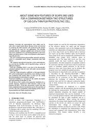
<strong>Scientific</strong> Bulletin <strong>of</strong> the Electrical Engineering Faculty – 2008A COMPARATIVE STUDY OF SEPIC, CUK AND ZETA CONVERTERSFlorian ION 1 , Gabriel PREDUSCA 2Abstract: In this paper a <strong>comparative</strong> <strong>study</strong> <strong>of</strong> DC-DC<strong>converters</strong> is presented. The SEPIC, Cuk <strong>and</strong> ZETA<strong>converters</strong> in applications are detailed. Also are presentedthe operating simulation for these <strong>converters</strong>. The results<strong>of</strong> simulations are compared with the measurements donefor a ZETA converter with an output <strong>of</strong> 3.3V <strong>and</strong> differentoutput currents.Keywords: DC-DC <strong>converters</strong>, SEPIC converter, Cukconverter, ZETA converter2.1. OPERATING PRINCIPLES2.1 Fundamental DC-DC ConvertersFrom the viewpoint <strong>of</strong> input <strong>and</strong> output voltages – V 1<strong>and</strong> V o , the fundamental <strong>converters</strong> are: (1) step-down orbuck <strong>converters</strong>, (2) step-up or boost <strong>converters</strong>, (3) stepdown/up or buck-boost <strong>converters</strong>. Figure 1 shows theprinciple diagrams <strong>of</strong> these topologies.1. INTRODUCTIONL1SL2It’s well known that to have the maximum efficiency<strong>of</strong> the solar panels, the load must be connected to thesolar panel through a DC-DC converter. The topologies<strong>and</strong> the operation <strong>of</strong> these <strong>converters</strong> are very welldescribed in the literature. A classification <strong>of</strong> these<strong>converters</strong> is presented in [1]. The authors <strong>of</strong> [1]consider the DC-DC <strong>converters</strong> in six decades: (1)classical/traditional <strong>converters</strong>, (2) multiple-quadrant<strong>converters</strong>, (3) switched component <strong>converters</strong>, (4) s<strong>of</strong>tswitching<strong>converters</strong>, (5) synchronous rectifier<strong>converters</strong>, (6) multiple energy-storage elementsresonant <strong>converters</strong>. The classical/traditional <strong>converters</strong>are divided in five categories: (1) fundamental<strong>converters</strong>, (2) transformer-type <strong>converters</strong>, (3)developed <strong>converters</strong>, (4) voltage-lift <strong>converters</strong>, <strong>and</strong> (5)super-lift <strong>converters</strong>.The <strong>converters</strong> studied in this paper are classicaldeveloped <strong>converters</strong> well known in literature like<strong>converters</strong> in SEPIC (Single Ended Primary InductanceConverter) topology, Cuk <strong>and</strong> ZETA (Positive OutputLuo Converter). The developed-type <strong>converters</strong> derivedfrom fundamental <strong>converters</strong> by addition <strong>of</strong> a low-passfilter. In [2] these <strong>converters</strong> are considered like aMASTER converter switched by a PWM signal, <strong>and</strong> aSLAVE converter achieved with passive components.Because the great usage <strong>of</strong> <strong>converters</strong> in thetopologies mentioned above in applications, we foundopportunity for a short presentation <strong>of</strong> operatingprinciples, simulations <strong>and</strong> some experimental resultsin this work. The equations <strong>of</strong> main operatingparameters, advantages <strong>and</strong> disadvantages <strong>of</strong> eachtopology are presented in chapter 2 <strong>of</strong> this paper. Thesimulations <strong>and</strong> the measurements are presented inchapter 3, <strong>and</strong> the final conclusions in chapter 4.V1V1V1L1L1C1SC1DSa)b)c)Figure 1. Fundamental DC-DC Converters: a) buckconverter, b) boost converter, c) buck-boost converter.In ideal operating conditions (no voltage loss on theswitch S, the average voltage across inductors L atsteady state zero, no current loss on capacitors C, <strong>and</strong>no voltage loss on diode at forward conduction) theequations <strong>of</strong> ratio V o /V 1 are:– for the buck converter (1):V o= D (1)V1where D is the duty cycle <strong>of</strong> PWM signal <strong>of</strong> switch S,with the meaning from equation (2),tOND = (2)TDC1L1L2DCoCoCoRsRsRs1 Valahia University/Electronic Department, Targoviste, Romania, e-mail: flion@valahia.ro2 Valahia University/Electronic Department, Targoviste, Romania, e-mail: gpredusca@valahia.ro17
<strong>Scientific</strong> Bulletin <strong>of</strong> the Electrical Engineering Faculty – 2008where t ON is the conduction time <strong>of</strong> switch S <strong>and</strong> T isthe period <strong>of</strong> PWM signal.– for the boost converter (3):V o 1= (3)V 1 − D– for the buck-boost converter (4):V o D=V 1 − D11(4)In all these equations the internal resistance <strong>of</strong>power supply V 1 was considered zero [3].V1V1L1L1SSCCa)L2DDL2CoCoRsRs2.2. Developed DC-DC <strong>converters</strong>b)Figure 2 shows the topologies <strong>of</strong> developed DC-DC<strong>converters</strong>.These topologies have few similitudes:– The equation <strong>of</strong> the transfer function <strong>of</strong> these<strong>converters</strong> is (4), the same with that one <strong>of</strong> buck-boostconverter, if the conditions <strong>of</strong> Continuous ConductionMode – CCM are assured.– These <strong>converters</strong> are used in differentapplications, such as with solar panels, in systemssupplied with electrical energy where the outputvoltage V o <strong>of</strong> converter can be superior or inferior <strong>of</strong>the input voltage V 1 <strong>of</strong> converter. The fundamental<strong>converters</strong> don’t accept this situation. These <strong>converters</strong>are integrated in the MPPT <strong>of</strong> solar panels.– The capacitor C assures the galvanic insulationbetween input <strong>and</strong> output. The short-circuits or othersbreakdown <strong>of</strong> the load don’t affect the power supply –solar panels.– The output voltage becomes zero if the PWMcontrol signal <strong>of</strong> switch S is missing.– The diode D can be replaced by a transistorswitched synchronal with the main switch in thesynchronous <strong>converters</strong>.The differences between these topologies are:– SEPIC <strong>and</strong> Cuk <strong>converters</strong> became from the boostconverter, <strong>and</strong> ZETA converter from the buck-boostconverter.– The ripple current in the load is greater for Cuk<strong>and</strong> ZETA <strong>converters</strong> than SEPIC, because the SEPICconverter has an inductor L 2 that smooth the currentspikes.– The switch S <strong>of</strong> SEPIC ad Cuk <strong>converters</strong> is a Nchannel MOS transistor that needs a Low Side driver,when the ZETA converter has a P channel MOStransistor that needs a High Side driver.Because, these three topologies have manyadvantages mentioned above, these things makeenable their integration in applications with a greatefficiency <strong>of</strong> using the solar energy in solar panelswith MPP trackers.V1SL1Cc)Figure 2. Developed DC-DC Converters: a) SEPICconverter, b) Cuk converter, c) ZETA converter2.3 Integration <strong>of</strong> convertors in MPPT systemsThe perturb-<strong>and</strong>–observe (PAO) method for theMPPT is an iterative approach. The MPP is obtainedby making the derivate <strong>of</strong> power equal with zero in thefeedback circuit that comm<strong>and</strong>s the duty cycle <strong>of</strong>switch S. This is very useful because doesn’t need thedisconnection <strong>of</strong> panels from the load. Through thismethod can be reached good results if it is compared theinstantaneous conductance <strong>of</strong> panel with the incrementalconductance <strong>of</strong> panel – the method is known asIncremental Conductance Technique (ICT) [4].If it is considered the equivalent circuit <strong>of</strong> the solarpanel like in Fig. 3, with v i the input voltage <strong>of</strong> panel<strong>and</strong> r i the equivalent input resistance <strong>of</strong> panel, P i theinput power, P o the output power (5), the∂P = 0 means (6).2viPi= Po=(5)ri∂viVi=(6)∂ri2RiThe method proposed in [4] resides in theconnection <strong>of</strong> a SEPIC or Cuk converter between thesolar panel <strong>and</strong> load. The converter works incontinuous current mode (CCM) through inductor L 1 –Figure 2 a), but with discontinuous voltage (DCV) onthe capacitor C. The duty cycle <strong>of</strong> PWM signal <strong>of</strong>switch is adjusted in a proper way to achieve the inputresistance <strong>of</strong> converter equal with the output resistance<strong>of</strong> solar panel. Figure 3 shows the equivalent circuit <strong>of</strong>solar panel <strong>and</strong> converter.DL2CoRs18
<strong>Scientific</strong> Bulletin <strong>of</strong> the Electrical Engineering Faculty – 2008Figure 3. Equivalent circuit <strong>of</strong> a solar panel <strong>and</strong>converter [4]The operating equations <strong>of</strong> SEPIC converter inDCV mode are the next: (7a) – the voltage oncapacitor C, (7b) – the voltage on diode D.vC⎧ I1(1− d)TS⎪ −V⎪C( t)= ⎨−Vo,⎪I⎪1( t − dT −S ) V⎩ Coo,I 2− t,0 < t < d1TSCd T < t < dT1dTSS< t < TSS(7a)vD⎧Vo + vC( t),0 < t < d1TS( t)= ⎨(7b)⎩0,d1TS< t < TSwhere I 1 <strong>and</strong> I 2 are the inductor currents - assumed tobe constant, dT S is the conduction time <strong>of</strong> switch, d 1 T Sis the conduction time <strong>of</strong> diode D, <strong>and</strong> T S is the period1<strong>of</strong> PWM signal <strong>of</strong> switch - TS= , f S – frequency <strong>of</strong>fPWM signal.The three sequences in one switching cycle areshown in Figure 4.Because the voltage <strong>of</strong> capacitor C at d 1 T SI1is vC( d 1 TS) = −Vo , the duty cycle is d1 = (1 − d).IIn the steady state the voltage on the inductor L 2 iszero. From this moment the output voltage V o is equalwith the average voltage <strong>of</strong> diode D (8).Vo1 d1TSTS= v ( t)dt I1(1d)d1T ∫ D = − (8)02CSMoreover, the voltage stress on the switch S isgiven by (9).In the same way can be determined the operatingequations <strong>of</strong> Cuk <strong>and</strong> ZETA topologies. This isshown in [4].I1v stres = vC( TS) + Vo= (1 − d)TS(9)CS2Figure 4. Operating principle <strong>of</strong> the SEPIC converter.a) equivalent circuits, b) theoretical waveforms [4]3. SimulationsIn this chapter it will be presented fewrepresentative waveforms <strong>of</strong> each topology. Thesimulations were done in OrCAD, in the nextconditions:– input voltage – V 1 =12V,– output voltage – V o =3.3V,– load resistance – R S =3.3Ω,– duty cycle – D=0.22,– switching frequency – f S =500kHz,– coupling capacitor C=47μF,– output capacitor C o =100μF,– inductors L 1 =L 2 =6.2μH.3.1 The SEPIC converterTo simulate the operation <strong>of</strong> SEPIC <strong>converters</strong> itwas used the diagram from Figure 2 a). In Figure 5 a),b), <strong>and</strong> c), is shown the output voltage V o , the ripple <strong>of</strong>19
<strong>Scientific</strong> Bulletin <strong>of</strong> the Electrical Engineering Faculty – 2008output voltage ΔV o , <strong>and</strong> the voltage stress V stress <strong>of</strong>switch S.At steady state – after 1.5ms, these values are:V 0 =3.5V, ΔV o =6mV pp , <strong>and</strong> V stress =16V.0V-2.0V6.0V-4.0V4.0V2.0V-6.0V0s 0.5ms 1.0ms 1.5ms 2.0ms 2.5ms 3.0ms 3.5ms 4.0msV(R4:2)Timea) V o – output voltage0V-3.60V-2.0V0s 0.5ms 1.0ms 1.5ms 2.0ms 2.5ms 3.0ms 3.5ms 4.0msV(R4:2)Timea) V o – output voltage-3.65V-3.70V3.7200V-3.75V3.7150V3.7100V-3.80V0.8773ms 0.9000ms 0.9500ms 1.0000ms 1.0500ms 1.1000msV(R4:2)Timeb) ΔV o – output ripple20V3.7056V2.960ms 2.962ms 2.964ms 2.966ms 2.968ms 2.970ms 2.972ms 2.974ms 2.976ms 2.978msV(R4:2)Timeb) ΔV o – output ripple15V10V20V5V15V10V0V877.34us 878.00us 879.00us 880.00us 881.00us 882.00us 883.00us 884.00usV(M2:d)Timec) V stress – voltage stress on switch5V0V2.96000ms 2.96400ms 2.96800ms 2.97200ms 2.97600ms 2.97897msV(M2:d)Timec) V stress – voltage stress on switchFigure 5. Simulated waveforms <strong>of</strong> SEPIC converter: a)output voltage, b) output ripple, c) voltage stress <strong>of</strong> switch3.2. The Cuk conveterTo simulate the operation <strong>of</strong> Cuk converter it wasused the diagram from Figure 2 b). Figure 6 a), b) <strong>and</strong>c) shows the waveforms <strong>of</strong> output voltage, outputripple <strong>and</strong> voltage stress <strong>of</strong> switch in the sameconditions.At steady state – after 0.5ms, these values are:V 0 =3.51V, ΔV o =28mV pp , <strong>and</strong> V stress =16V.3.3. The ZETA converterTo simulate the operation <strong>of</strong> ZETA converter it wasused the diagram from Figure 2 c). Figure 7 a), b) <strong>and</strong> c)shows the waveforms <strong>of</strong> output voltage, output ripple<strong>and</strong> voltage stress <strong>of</strong> switch in the same conditions.At steady state – after 0.5ms, these values are:V 0 =3.41V, ΔV o =26mV pp , <strong>and</strong> V stress =16V.Figure 6. Simulated waveforms <strong>of</strong> Cuk converter: a)output voltage, b) output ripple, c) voltage stress <strong>of</strong> switchConclusions on simulations are in Table 1.Table 1. Simulation ResultsVoltageTopologySEPIC Cuk ZETAV o [V] 3.51 3.51 3.41ΔV o [mV pp ] 6 28 26V stress [V] 16 16 163.4. Experimental verificationsAn experiment has been performed using a ZETAtopology on a LTC1622 – a Current Mode Step-DownDC/DC converter <strong>of</strong> Linear Technology [5]. Theschematic diagram is the typical application proposedby the producer <strong>and</strong> is shown in Figure 8 [6].In Figure 9 are the waveforms in the nextconditions: V 1 =8.3V, V o =3.3V, R S =20Ω (I o =165mA).The channels <strong>of</strong> oscilloscope represent: CH1 – V G –PWM signal on the gate <strong>of</strong> MOS transistor, CH2 – V D– drain voltage <strong>of</strong> MOS transistor, CH3 – V C – voltage20
<strong>Scientific</strong> Bulletin <strong>of</strong> the Electrical Engineering Faculty – 2008on positive pin <strong>of</strong> capacitor C, CH4 – ΔV o – outputvoltage ripple.In Figure 10 are the waveforms in these conditions:V 1 =4.9V, V o =3.4V, R S =10Ω (I o =340mA). It can beobserved other values for switching frequency <strong>and</strong>duty cycle <strong>of</strong> PWM signal.6.0V4.0V2.0Vsystems where these conditions are reached very <strong>of</strong>ten –like solar panels in different levels <strong>of</strong> solar radiation.The results <strong>of</strong> measurements are in Table 2.The circuit LTC1622 changes the switchingfrequency – Figure 9, 10, 11, in a wide range – from265 kHz to 1024 kHz. Also, the duty cycle D <strong>of</strong> PWMsignal in the gate <strong>of</strong> the MOS transistor is changedaccording with the work conditions – input <strong>and</strong> outputvoltage, <strong>and</strong> the output current, to insure a constantvalue <strong>of</strong> output voltage.The ripple <strong>of</strong> output voltage measured in realconditions is few times greater than that one obtainedin ideal conditions <strong>of</strong> simulations.0V0s 0.5ms 1.0ms 1.5ms 2.0ms 2.5ms 3.0ms 3.5ms 4.0msV(R8:2)Timea) V o – output voltage3.62V3.61V3.60V3.59V4.65ms 4.70ms 4.75ms 4.80ms 4.85ms 4.90ms 4.95ms 5.00msV(R8:2)Timeb) ΔV o – output ripple20V15V10VFigure 9. Waveforms <strong>of</strong> V G , V D , V C , ΔV o in conditions:V 1 =8.3V, V o =3.3V, R S =20Ω5V0V4.650ms 4.652ms 4.654ms 4.656ms 4.658ms 4.660msV(M1:s)- V(M1:d)Timec) V stress – voltage stress on switchFigure 7. Simulated waveforms <strong>of</strong> ZETA converter: a)output voltage, b) output ripple, c) voltage stress <strong>of</strong> switchFigure 8. ZETA converter with LTC1622 [9]The experimental waveforms in the conditions:V 1 =7.1V, V o =3.4V, R S =5Ω (I o =680mA) are shown inFigure 11.It can be seen that the ZETA converter build with theLTC1622 integrated circuit works well with inputvoltages less than output voltage <strong>and</strong> at an input voltageover the output voltage. This advantage can be used inFigure 10. Waveforms <strong>of</strong> V G , V D , V C , ΔV o in conditions:V 1 =4.9V, V o =3.4V, R S =10Ω21
<strong>Scientific</strong> Bulletin <strong>of</strong> the Electrical Engineering Faculty – 2008REFERENCESFigure 11. Waveforms <strong>of</strong> V G , V D , V C , ΔV o in conditions:V 1 =7,1V, V o =3,4V, R S =5Ω[1] F. L. Luo, H. Ye, “Advanced DC/DC Converters”,CRC Press, 2004.[2] S. Maniktala, “Slave Converters Power AuxiliaryOutputs”, EDN Magazine, Elsevier, 2002.[3] P. Constantin, et al., “Electronică industrială”, EdituraDidactică şi Pedagogică, Bucureşti, 1983.[4] H. S-H. Chung, et al., “A Novel Maximum PowerPoint Tracking Technique for Solar Panels Using aSEPIC or Cuk Converter”, IEEE Transaction on PowerElectronics, Vol. 18, No. 3, May 2003.[5] M. Dobre, F. Ion - supervisor, “Corecţia factorului deputere în convertoarele în comutaţie cu reţele decomutare de ordin zero”, Proiect de diplomă,Universitatea Valahia, Târgovişte, iulie 2007.***, “LTC1622 Low Voltage Input Current Mode Step-Down DC/DC Controller”, Data Sheet, LinearTechnology, 1998.Table 2. Measurement resultsZETA converter with LTC1622with output voltage 3.3VVoltageV 1 =8.3V, V 1 =4.8V, V 1 =3.2V,I o =165mA I o =165mA I o =165mAΔV o [V pp ] 1.37 0.82 0.60f S [kHz] 265 524 504VoltageV 1 =8.3V, V 1 =4.9V, V 1 =8.3V, V 1 =7.1V,I o =340mA I o =340mA I o =680mA I o =680mAΔV o [V pp ] 1.25 0.83 1.45 1.12f S [kHz] 913 759 1024 5624. CONCLUSIONSIn this paper was presented a <strong>comparative</strong> <strong>study</strong> <strong>of</strong>DC-DC <strong>converters</strong> in SEPIC, Cuk <strong>and</strong> ZETAtopologies.It was studied the fundamental <strong>converters</strong> <strong>and</strong>developed <strong>converters</strong> in the topologies mentionedabove. The operation equations <strong>of</strong> main parameterswere presented.Moreover, it was presented the simulations <strong>of</strong> these<strong>converters</strong> in the same work conditions.The waveforms that have seen on a ZETAconverter with a constant output voltage <strong>and</strong> variableinput voltage <strong>and</strong> load confirmed the simulationsresults <strong>of</strong> that converter.22