24AA512/24LC512/24FC512 - Microchip Taiwan
24AA512/24LC512/24FC512 - Microchip Taiwan
24AA512/24LC512/24FC512 - Microchip Taiwan

Create successful ePaper yourself
Turn your PDF publications into a flip-book with our unique Google optimized e-Paper software.
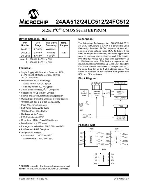
<strong>24AA512</strong>/<strong>24LC512</strong>/<strong>24FC512</strong>512K I 2 C CMOS Serial EEPROMDevice Selection TablePartNumberFeatures:VCCRangeMax. ClockFrequencyTemp.Ranges<strong>24AA512</strong> 1.7-5.5V 400 kHz (1) I<strong>24LC512</strong> 2.5-5.5V 400 kHz I, E<strong>24FC512</strong> 1.7-5.5V 1 MHz (2) INote 1: 100 kHz for VCC < 2.5V2: 400 kHz for VCC < 2.5V• Single Supply with Operation Down to 1.7V for<strong>24AA512</strong> and <strong>24FC512</strong> Devices, 2.5V for<strong>24LC512</strong> Devices• Low-Power CMOS Technology:- Active current 400 uA, typical- Standby current 100 nA, typical• 2-Wire Serial Interface, I 2 C Compatible• Cascadable for up to Eight Devices• Schmitt Trigger Inputs for Noise Suppression• Output Slope Control to Eliminate Ground Bounce• 100 kHz and 400 kHz Clock Compatibility• Page Write Time 5 ms max.• Self-Timed Erase/Write Cycle• 128-Byte Page Write Buffer• Hardware Write-Protect• ESD Protection >4000V• More than 1 Million Erase/Write Cycles• Data Retention > 200 years• Packages Include 8-lead PDIP, SOIJ and DFN• Pb-Free and RoHS Compliant• Temperature Ranges:- Industrial (I): -40°C to +85°C- Automotive (E):-40°C to +125°CDescription:The <strong>Microchip</strong> Technology Inc. <strong>24AA512</strong>/<strong>24LC512</strong>/<strong>24FC512</strong> (24XX512*) is a 64K x 8 (512 Kbit) SerialElectrically Erasable PROM, capable of operationacross a broad voltage range (1.7V to 5.5V). It hasbeen developed for advanced, low-power applicationssuch as personal communications and data acquisition.This device also has a page write capability of upto 128 bytes of data. This device is capable of bothrandom and sequential reads up to the 512K boundary.Functional address lines allow up to eight devices onthe same bus, for up to 4 Mbit address space. Thisdevice is available in the standard 8-pin plastic DIP,SOIJ and DFN packages.Block DiagramI/OControlLogicI/OSDAVCCVSSSCLPackage TypeA0A1A2VSS123424XX512A0 A1 A2 WPPDIPMemoryControlLogic8765XDECVCCA0WP A1SCL A2SDA VSS1234HV GeneratorEEPROMArrayPage LatchesYDECSense Amp.R/W ControlSOIJ24XX5128765VCCWPSCLSDADFN* 24XX512 is used in this document as a generic partnumber for the <strong>24AA512</strong>/<strong>24LC512</strong>/<strong>24FC512</strong> devices.A0A1A2VSS1 8 VCC23424XX5127 WP6 SCL5 SDA© 2008 <strong>Microchip</strong> Technology Inc. DS21754J-page 1
<strong>24AA512</strong>/<strong>24LC512</strong>/<strong>24FC512</strong>1.0 ELECTRICAL CHARACTERISTICSAbsolute Maximum Ratings (†)VCC.............................................................................................................................................................................6.5VAll inputs and outputs w.r.t. VSS ......................................................................................................... -0.6V to VCC +1.0VStorage temperature ...............................................................................................................................-65°C to +150°CAmbient temperature with power applied................................................................................................-40°C to +125°CESD protection on all pins ......................................................................................................................................................≥ 4kV† NOTICE: Stresses above those listed under “Absolute Maximum Ratings” may cause permanent damage to thedevice. This is a stress rating only and functional operation of the device at those or any other conditions above thoseindicated in the operational listings of this specification is not implied. Exposure to maximum rating conditions forextended periods may affect device reliability.TABLE 1-1: DC CHARACTERISTICSElectrical Characteristics:DC CHARACTERISTICSIndustrial (I): VCC = +1.7V to 5.5V TA = -40°C to +85°CAutomotive (E): VCC = +2.5V to 5.5V TA = -40°C to +125°CParam.No.Sym. Characteristic Min. Max. Units ConditionsD1 — A0, A1, A2, SCL, SDA — — — —and WP pins:D2 VIH High-level input voltage 0.7 VCC — V —D3 VIL Low-level input voltage — 0.3 VCC0.2 VCCD4 VHYS Hysteresis of SchmittTrigger inputs(SDA, SCL pins)VVVCC ≥ 2.5VVCC < 2.5V0.05 VCC — V VCC ≥ 2.5V (Note)D5 VOL Low-level output voltage — 0.40 V IOL = 3.0 ma @ VCC = 4.5VIOL = 2.1 ma @ VCC = 2.5VD6 ILI Input leakage current — ±1 μA VIN = VSS or VCC, WP = VSSVIN = VSS or VCC, WP = VCCD7 ILO Output leakage current — ±1 μA VOUT = VSS or VCCD8 CIN,COUTPin capacitance(all inputs/outputs)— 10 pF VCC = 5.0V (Note)TA = 25°C, FCLK = 1 MHzD9 ICC Read Operating current — 400 μA VCC = 5.5V, SCL = 400 kHzICC Write — 5 mA VCC = 5.5VD10 ICCS Standby current — 1 μA TA = -40°C to +85°CSCL = SDA = VCC = 5.5VA0, A1, A2, WP = VSS— 5 μA TA = -40°C to +125°CSCL = SDA = VCC = 5.5VA0, A1, A2, WP = VSSNote: This parameter is periodically sampled and not 100% tested.DS21754J-page 2© 2008 <strong>Microchip</strong> Technology Inc.
<strong>24AA512</strong>/<strong>24LC512</strong>/<strong>24FC512</strong>TABLE 1-2:AC CHARACTERISTICSParam.No.AC CHARACTERISTICSElectrical Characteristics:Industrial (I): VCC = +1.7V to 5.5V TA = -40°C to +85°CAutomotive (E): VCC = +2.5V to 5.5V TA = -40°C to +125°CSym. Characteristic Min. Max. Units Conditions1 FCLK Clock frequency ————2 THIGH Clock high time 40006006005003 TLOW Clock low time 4700130013005004 TR SDA and SCL rise time (Note 1) ———5 TF SDA and SCL fall time (Note 1) ——6 THD:STA Start condition hold time 40006006002507 TSU:STA Start condition setup time 47006006002501004004001000————————10003003008 THD:DAT Data input hold time 0 — ns (Note 2)9 TSU:DAT Data input setup time 25010010010 TSU:STO Stop condition setup time 400060060025011 TSU:WP WP setup time 400060060012 THD:WP WP hold time 47001300130013 TAA Output valid from clock (Note 2) ————14 TBUF Bus free time: Time the busmust be free before a new transmissioncan start470013001300500300100—————————————————————3500900900400————kHz 1.7V ≤ VCC < 2.5V2.5V ≤ VCC ≤ 5.5V1.7V ≤ VCC < 2.5V <strong>24FC512</strong>2.5V ≤ VCC ≤ 5.5V <strong>24FC512</strong>ns 1.7V ≤ VCC < 2.5V2.5V ≤ VCC ≤ 5.5V1.7V ≤ VCC < 2.5V <strong>24FC512</strong>2.5V ≤ VCC ≤ 5.5V <strong>24FC512</strong>ns 1.7V ≤ VCC < 2.5V2.5V ≤ VCC ≤ 5.5V1.7V ≤ VCC < 2.5V <strong>24FC512</strong>2.5V ≤ VCC ≤ 5.5V <strong>24FC512</strong>ns 1.7V ≤ VCC< 2.5V2.5V ≤ VCC ≤ 5.5V1.7V ≤ VCC ≤ 5.5V <strong>24FC512</strong>nsAll except, <strong>24FC512</strong>1.7V ≤ VCC ≤ 5.5V <strong>24FC512</strong>ns 1.7V ≤ VCC < 2.5V2.5V ≤ VCC ≤ 5.5V1.7V ≤ VCC < 2.5V <strong>24FC512</strong>2.5V ≤ VCC ≤ 5.5V <strong>24FC512</strong>ns 1.7V ≤ VCC < 2.5V2.5V ≤ VCC ≤ 5.5V1.7V ≤ VCC < 2.5V <strong>24FC512</strong>2.5V ≤ VCC ≤ 5.5V <strong>24FC512</strong>ns 1.7V ≤ VCC < 2.5V2.5V ≤ VCC ≤ 5.5V1.7V ≤ VCC ≤ 5.5V <strong>24FC512</strong>ns 1.7V ≤ VCC < 2.5V2.5V ≤ VCC ≤ 5.5V1.7V ≤ VCC < 2.5V <strong>24FC512</strong>2.5V ≤ VCC ≤ 5.5V <strong>24FC512</strong>ns 1.7V ≤ VCC < 2.5V2.5V ≤ VCC ≤ 5.5V1.7V ≤ VCC ≤ 5.5V <strong>24FC512</strong>ns 1.7V ≤ VCC < 2.5V2.5V ≤ VCC ≤ 5.5V1.7V ≤ VCC ≤ 5.5V <strong>24FC512</strong>ns 1.7V ≤ VCC < 2.5V2.5V ≤ VCC ≤ 5.5V1.7V ≤ VCC < 2.5V <strong>24FC512</strong>2.5V ≤ VCC ≤ 5.5V <strong>24FC512</strong>ns 1.7V ≤ VCC < 2.5V2.5V ≤ VCC ≤ 5.5V1.7V ≤ VCC < 2.5V <strong>24FC512</strong>2.5V ≤ VCC ≤ 5.5V <strong>24FC512</strong>Note 1: Not 100% tested. CB = total capacitance of one bus line in pF.2: As a transmitter, the device must provide an internal minimum delay time to bridge the undefined region (minimum300 ns) of the falling edge of SCL to avoid unintended generation of Start or Stop conditions.3: The combined TSP and VHYS specifications are due to new Schmitt Trigger inputs which provide improved noise spikesuppression. This eliminates the need for a TI specification for standard operation.4: This parameter is not tested but ensured by characterization. For endurance estimates in a specific application, pleaseconsult the Total Endurance Model which can be obtained from <strong>Microchip</strong>’s web site at www.microchip.com.© 2008 <strong>Microchip</strong> Technology Inc. DS21754J-page 3
<strong>24AA512</strong>/<strong>24LC512</strong>/<strong>24FC512</strong>AC CHARACTERISTICS (Continued)Param.No.16 TSP Input filter spike suppression(SDA and SCL pins)Electrical Characteristics:Industrial (I): VCC = +1.7V to 5.5V TA = -40°C to +85°CAutomotive (E): VCC = +2.5V to 5.5V TA = -40°C to +125°CSym. Characteristic Min. Max. Units Conditions17 TWC Write cycle time (byte or page) — 5 ms —— 50 ns All except, <strong>24FC512</strong> (Notes 1 and 3)18 — Endurance 1,000,000 — cycles 25°C (Note 4)Note 1: Not 100% tested. CB = total capacitance of one bus line in pF.2: As a transmitter, the device must provide an internal minimum delay time to bridge the undefined region (minimum300 ns) of the falling edge of SCL to avoid unintended generation of Start or Stop conditions.3: The combined TSP and VHYS specifications are due to new Schmitt Trigger inputs which provide improved noise spikesuppression. This eliminates the need for a TI specification for standard operation.4: This parameter is not tested but ensured by characterization. For endurance estimates in a specific application, pleaseconsult the Total Endurance Model which can be obtained from <strong>Microchip</strong>’s web site at www.microchip.com.DS21754J-page 4© 2008 <strong>Microchip</strong> Technology Inc.
<strong>24AA512</strong>/<strong>24LC512</strong>/<strong>24FC512</strong>FIGURE 1-1:BUS TIMING DATA52D44SCLSDAIN167638 910SDAOUT1314WP(protected)(unprotected)11 12© 2008 <strong>Microchip</strong> Technology Inc. DS21754J-page 5
<strong>24AA512</strong>/<strong>24LC512</strong>/<strong>24FC512</strong>2.0 PIN DESCRIPTIONSThe descriptions of the pins are listed in Table 2-1.TABLE 2-1:PIN FUNCTION TABLEName PDIP SOIJ DFN FunctionA0 1 1 1 User Configured Chip SelectA1 2 2 2 User Configured Chip Select(NC) — — — Not ConnectedA2 3 3 3 User Configured Chip SelectVSS 4 4 4 GroundSDA 5 5 5 Serial DataSCL 6 6 6 Serial Clock(NC) — — — Not ConnectedWP 7 7 7 Write-Protect InputVCC 8 8 8 +1.7V to 5.5V (<strong>24AA512</strong>)+2.5V to 5.5V (<strong>24LC512</strong>)+1.7V to 5.5V (<strong>24FC512</strong>)2.1 A0, A1 and A2 Chip AddressInputsThe A0, A1 and A2 inputs are used by the 24XX512 formultiple device operations. The logic levels on theseinputs are compared with the corresponding bits in theslave address. The chip is selected if the compare istrue.Up to eight devices may be connected to the same busby using different Chip Select bit combinations. Theseinputs must be connected to either VCC or VSS.In most applications, the chip address inputs A0, A1and A2 are hard-wired to logic ‘0’ or logic ‘1’. Forapplications in which these pins are controlled by amicrocontroller or other programmable logic device,the chip address pins must be driven to logic ‘0’ or logic‘1’ before normal device operation can proceed.2.2 Serial Data (SDA)This is a bidirectional pin used to transfer addressesand data into and data out of the device. It is an opendrainterminal, therefore, the SDA bus requires a pullupresistor to VCC (typical 10 kΩ for 100 kHz, 2 kΩ for400kHz and 1MHz).For normal data transfer, SDA is allowed to changeonly during SCL low. Changes during SCL high arereserved for indicating the Start and Stop conditions.2.3 Serial Clock (SCL)This input is used to synchronize the data transfer fromand to the device.2.4 Write-Protect (WP)This pin must be connected to either VSS or VCC. If tiedto VSS, write operations are enabled. If tied to VCC,write operations are inhibited but read operations arenot affected.3.0 FUNCTIONAL DESCRIPTIONThe 24XX512 supports a bidirectional 2-wire bus anddata transmission protocol. A device that sends dataonto the bus is defined as a transmitter and a devicereceiving data as a receiver. The bus must becontrolled by a master device which generates theSerial Clock (SCL), controls the bus access andgenerates the Start and Stop conditions, while the24XX512 works as a slave. Both master and slavecan operate as a transmitter or receiver, but themaster device determines which mode is activated.DS21754J-page 6© 2008 <strong>Microchip</strong> Technology Inc.
<strong>24AA512</strong>/<strong>24LC512</strong>/<strong>24FC512</strong>4.0 BUS CHARACTERISTICSThe following bus protocol has been defined:• Data transfer may be initiated only when the busis not busy.• During data transfer, the data line must remainstable whenever the clock line is high. Changes inthe data line, while the clock line is high, will beinterpreted as a Start or Stop condition.Accordingly, the following bus conditions have beendefined (Figure 4-1).4.1 Bus Not Busy (A)Both data and clock lines remain high.4.2 Start Data Transfer (B)A high-to-low transition of the SDA line while the clock(SCL) is high determines a Start condition. Allcommands must be preceded by a Start condition.4.5 AcknowledgeEach receiving device, when addressed, is obliged togenerate an Acknowledge signal after the reception ofeach byte. The master device must generate an extraclock pulse which is associated with this Acknowledgebit. See Figure 4-2 for acknowledge timing.Note:The 24XX512 does not generate anyAcknowledge bits if an internal programmingcycle is in progress.A device that acknowledges must pull down the SDAline during the Acknowledge clock pulse in such a waythat the SDA line is stable low during the high period ofthe acknowledge related clock pulse. Of course, setupand hold times must be taken into account. Duringreads, a master must signal an end of data to the slaveby NOT generating an Acknowledge bit on the last bytethat has been clocked out of the slave. In this case, theslave (24XX512) will leave the data line high to enablethe master to generate the Stop condition.4.3 Stop Data Transfer (C)A low-to-high transition of the SDA line while the clock(SCL) is high determines a Stop condition. Alloperations must end with a Stop condition.4.4 Data Valid (D)The state of the data line represents valid data when,after a Start condition, the data line is stable for theduration of the high period of the clock signal.The data on the line must be changed during the lowperiod of the clock signal. There is one bit of data perclock pulse.Each data transfer is initiated with a Start condition andterminated with a Stop condition. The number of thedata bytes transferred between the Start and Stopconditions is determined by the master device.© 2008 <strong>Microchip</strong> Technology Inc. DS21754J-page 7
<strong>24AA512</strong>/<strong>24LC512</strong>/<strong>24FC512</strong>FIGURE 4-1:DATA TRANSFER SEQUENCE ON THE SERIAL BUSSCL(A) (B) (D) (D) (C) (A)SDAStartConditionAddress orAcknowledgeValidDataAllowedto ChangeStopConditionFIGURE 4-2:ACKNOWLEDGE TIMINGAcknowledgeBitSCL 1 2 3 4 5 6 7 8 9 1 2 3SDAData from transmitterTransmitter must release the SDA line at this pointallowing the Receiver to pull the SDA line low toacknowledge the previous eight bits of data.Data from transmitterReceiver must release the SDA lineat this point so the Transmitter cancontinue sending data.DS21754J-page 8© 2008 <strong>Microchip</strong> Technology Inc.
<strong>24AA512</strong>/<strong>24LC512</strong>/<strong>24FC512</strong>5.0 DEVICE ADDRESSINGFIGURE 5-1:CONTROL BYTE FORMATA control byte is the first byte received following theStart condition from the master device (Figure 5-1).The control byte consists of a 4-bit control code; for the24XX512 this is set as ‘1010’ binary for read and writeoperations. The next three bits of the control byte arethe Chip Select bits (A2, A1 and A0). The Chip Selectbits allow the use of up to eight 24XX512 devices onthe same bus and are used to select which device isaccessed. The Chip Select bits in the control byte mustcorrespond to the logic levels on the corresponding A2,A1 and A0 pins for the device to respond. These bitsare in effect the three Most Significant bits of the wordaddress.The last bit of the control byte defines the operation tobe performed. When set to a one a read operation isselected and when set to a zero a write operation isselected. The next two bytes received define theaddress of the first data byte (Figure 5-2). Because allA15…A0 are used, there are no upper address bits thatare “don’t care”. The upper address bits are transferredfirst, followed by the Less Significant bits.Following the Start condition, the 24XX512 monitorsthe SDA bus checking the device type identifier beingtransmitted. Upon receiving a ‘1010’ code and appropriatedevice select bits, the slave device outputs anAcknowledge signal on the SDA line. Depending on thestate of the R/W bit, the 24XX512 will select a read orwrite operation.SStart BitControl Code1 0 1 0 A2 A1 A0Slave AddressRead/Write BitChip SelectBitsR/WAcknowledge Bit5.1 Contiguous Addressing AcrossMultiple DevicesACKThe Chip Select bits A2, A1 and A0 can be used toexpand the contiguous address space for up to 4 Mbitby adding up to eight 24XX512 devices on the samebus. In this case, software can use A0 of the controlbyte as address bit A16; A1 as address bit A17; and A2as address bit A18. It is not possible to sequentiallyread across device boundaries.FIGURE 5-2:ADDRESS SEQUENCE BIT ASSIGNMENTSControl Byte Address High Byte Address Low Byte1 0 1 0A2A1A0 R/WA15A14A13A12A11A10 A 9A A A8 7• • • • • • 0ControlCodeChipSelectBits© 2008 <strong>Microchip</strong> Technology Inc. DS21754J-page 9
<strong>24AA512</strong>/<strong>24LC512</strong>/<strong>24FC512</strong>6.0 WRITE OPERATIONS6.1 Byte WriteFollowing the Start condition from the master, thecontrol code (four bits), the Chip Select (three bits) andthe R/W bit (which is a logic low) are clocked onto thebus by the master transmitter. This indicates to theaddressed slave receiver that the address high byte willfollow after it has generated an Acknowledge bit duringthe ninth clock cycle. Therefore, the next bytetransmitted by the master is the high-order byte of theword address and will be written into the AddressPointer of the 24XX512. The next byte is the LeastSignificant Address Byte. After receiving anotherAcknowledge signal from the 24XX512, the masterdevice will transmit the data word to be written into theaddressed memory location. The 24XX512 acknowledgesagain and the master generates a Stopcondition. This initiates the internal write cycle andduring this time, the 24XX512 will not generateAcknowledge signals (Figure 6-1). If an attempt ismade to write to the array with the WP pin held high, thedevice will acknowledge the command, but no writecycle will occur, no data will be written and the devicewill immediately accept a new command. After a byteWrite command, the internal address counter will pointto the address location following the one that was justwritten.6.3 Write ProtectionThe WP pin allows the user to write-protect the entirearray (0000-FFFF) when the pin is tied to VCC. If tied toVSS the write protection is disabled. The WP pin issampled at the Stop bit for every Write command(Figure 1-1). Toggling the WP pin after the Stop bit willhave no effect on the execution of the write cycle.Note:Page write operations are limited to writingbytes within a single physical page,regardless of the number of bytesactually being written. Physical pageboundaries start at addresses that areinteger multiples of the page buffer size (or‘page size’) and end at addresses that areinteger multiples of [page size – 1]. If aPage Write command attempts to writeacross a physical page boundary, theresult is that the data wraps around to thebeginning of the current page (overwritingdata previously stored there), instead ofbeing written to the next page as might beexpected. It is therefore necessary for theapplication software to prevent page writeoperations that would attempt to cross apage boundary.6.2 Page WriteThe write control byte, word address and the first databyte are transmitted to the 24XX512 in the same wayas in a byte write. But instead of generating a Stopcondition, the master transmits up to 127 additionalbytes, which are temporarily stored in the on-chip pagebuffer and will be written into memory after the masterhas transmitted a Stop condition. After receipt of eachword, the seven lower Address Pointer bits are internallyincremented by one. If the master should transmitmore than 128 bytes prior to generating the Stop condition,the address counter will roll over and the previouslyreceived data will be overwritten. As with the bytewrite operation, once the Stop condition is received, aninternal write cycle will begin (Figure 6-2). If an attemptis made to write to the array with the WP pin held high,the device will acknowledge the command, but no writecycle will occur, no data will be written and the devicewill immediately accept a new command.DS21754J-page 10© 2008 <strong>Microchip</strong> Technology Inc.
<strong>24AA512</strong>/<strong>24LC512</strong>/<strong>24FC512</strong>FIGURE 6-1:BYTE WRITEBus ActivityMasterSDA LineSTARTControlByteS 1010A A A2 1 00AddressHigh ByteAddressLow ByteDataSTOPPBus ActivityACKACKACKACKFIGURE 6-2:PAGE WRITEBus ActivityMasterSTARTControlByteAddressHigh ByteAddressLow Byte Data Byte 0Data Byte 127STOPSDA LineA A AS 1010 2 1 0 0PBus ActivityACKACKACKACKACK© 2008 <strong>Microchip</strong> Technology Inc. DS21754J-page 11
<strong>24AA512</strong>/<strong>24LC512</strong>/<strong>24FC512</strong>7.0 ACKNOWLEDGE POLLINGSince the device will not acknowledge during a writecycle, this can be used to determine when the cycle iscomplete (this feature can be used to maximize busthroughput). Once the Stop condition for a Writecommand has been issued from the master, the deviceinitiates the internally timed write cycle. ACK pollingcan be initiated immediately. This involves the mastersending a Start condition, followed by the control bytefor a Write command (R/W = 0). If the device is stillbusy with the write cycle, then no ACK will be returned.If no ACK is returned, then the Start bit and control bytemust be re-sent. If the cycle is complete, then thedevice will return the ACK and the master can thenproceed with the next Read or Write command. SeeFigure 7-1 for flow diagram.FIGURE 7-1:ACKNOWLEDGE POLLINGFLOWSendWrite CommandSend StopCondition toInitiate Write CycleSend StartSend Control Bytewith R/W = 0Did DeviceAcknowledge(ACK = 0)?NoYesNextOperationDS21754J-page 12© 2008 <strong>Microchip</strong> Technology Inc.
<strong>24AA512</strong>/<strong>24LC512</strong>/<strong>24FC512</strong>8.0 READ OPERATIONRead operations are initiated in the same way as writeoperations with the exception that the R/W bit of thecontrol byte is set to ‘1’. There are three basic types ofread operations: current address read, random readand sequential read.8.1 Current Address ReadThe 24XX512 contains an address counter that maintainsthe address of the last word accessed, internallyincremented by ‘1’. Therefore, if the previous readaccess was to address ‘n’ (n is any legal address), thenext current address read operation would access datafrom address n + 1.Upon receipt of the control byte with R/W bit set to ‘1’,the 24XX512 issues an acknowledge and transmits the8-bit data word. The master will not acknowledge thetransfer but does generate a Stop condition and the24XX512 discontinues transmission (Figure 8-1).8.3 Sequential ReadSequential reads are initiated in the same way as arandom read except that after the 24XX512 transmitsthe first data byte, the master issues an acknowledgeas opposed to the Stop condition used in a randomread. This acknowledge directs the 24XX512 totransmit the next sequentially addressed 8-bit word(Figure 8-3). Following the final byte transmitted to themaster, the master will NOT generate an acknowledge,but will generate a Stop condition. To providesequential reads, the 24XX512 contains an internalAddress Pointer which is incremented by one at thecompletion of each operation. This Address Pointerallows the entire memory contents to be serially readduring one operation. The internal Address Pointer willautomatically roll over from address FFFF to address0000 if the master acknowledges the byte receivedfrom the array address FFFF.FIGURE 8-1:Bus ActivityMasterSDA LineBus ActivityCURRENT ADDRESSREADSTA ControlR ByteTS 1 0 1 0 AAA 12 1 0ACKDataByteNOACKSTOPP8.2 Random ReadRandom read operations allow the master to accessany memory location in a random manner. To performthis type of read operation, first the word address mustbe set. This is done by sending the word address to the24XX512 as part of a write operation (R/W bit set to‘0’). After the word address is sent, the mastergenerates a Start condition following the acknowledge.This terminates the write operation, but not before theinternal Address Pointer is set. Then, the master issuesthe control byte again but with the R/W bit set to a one.The 24XX512 will then issue an acknowledge andtransmit the 8-bit data word. The master will notacknowledge the transfer but does generate a Stopcondition which causes the 24XX512 to discontinuetransmission (Figure 8-2). After a random Readcommand, the internal address counter will point to theaddress location following the one that was just read.© 2008 <strong>Microchip</strong> Technology Inc. DS21754J-page 13
<strong>24AA512</strong>/<strong>24LC512</strong>/<strong>24FC512</strong>FIGURE 8-2:RANDOM READBus ActivityMasterSTARTControlByteAddressHigh ByteAddressLow ByteSTARTControlByteDataByteSTOPSDA Line S 1010 AAA 0210ABus ActivityCKx = “don’t care” bitACKACKS 1010 AAA 1210ACKPNOACKFIGURE 8-3:Bus ActivityMasterSDA LineBus ActivitySEQUENTIAL READControlByte Data (n) Data (n + 1) Data (n + 2) Data (n + x)ACKACKACKACKNOACKSTOPPDS21754J-page 14© 2008 <strong>Microchip</strong> Technology Inc.
<strong>24AA512</strong>/<strong>24LC512</strong>/<strong>24FC512</strong>9.0 PACKAGING INFORMATION9.1 Package Marking Information8-Lead PDIP (300 mil)XXXXXXXXT/XXXNNNYYWWExample:<strong>24AA512</strong>I/P e3 01705108-Lead SOIJ (5.28 mm)XXXXXXXXT/XXXXXXYYWWNNNExample:<strong>24LC512</strong>I/SM e305100178-Lead DFN-SXXXXXXXT/XXXXXYYWWNNNExample:<strong>24LC512</strong>I/MF e30510017Legend: XX...X Customer-specific information*Y Year code (last digit of calendar year)YY Year code (last 2 digits of calendar year)WW Week code (week of January 1 is week ‘01’)NNNe3Alphanumeric traceability codePb-free JEDEC designator for Matte Tin (Sn)* This package is Pb-free. The Pb-free JEDEC designator ( e3 )can be found on the outer packaging for this package.T TemperatureBlank CommercialI IndustrialE ExtendedNote:In the event the full <strong>Microchip</strong> part number cannot be marked on one line, it willbe carried over to the next line, thus limiting the number of availablecharacters for customer-specific information.*Standard device marking consists of <strong>Microchip</strong> part number, year code, week code, and traceability code. Fordevice marking beyond this, certain price adders apply. Please check with your <strong>Microchip</strong> Sales Office.© 2008 <strong>Microchip</strong> Technology Inc. DS21754J-page 15
<strong>24AA512</strong>/<strong>24LC512</strong>/<strong>24FC512</strong>NNOTE 1E11 2 3DEAA2A1Lcb1beeB DS21754J-page 16© 2008 <strong>Microchip</strong> Technology Inc.
<strong>24AA512</strong>/<strong>24LC512</strong>/<strong>24FC512</strong>NDEE1b1 2eαAA2cφA1βL © 2008 <strong>Microchip</strong> Technology Inc. DS21754J-page 17
<strong>24AA512</strong>/<strong>24LC512</strong>/<strong>24FC512</strong>Note:For the most current package drawings, please see the <strong>Microchip</strong> Packaging Specification located athttp://www.microchip.com/packagingDS21754J-page 18© 2008 <strong>Microchip</strong> Technology Inc.
<strong>24AA512</strong>/<strong>24LC512</strong>/<strong>24FC512</strong>NDbeNLKEE2EXPOSED PADNOTE 1 1 2TOP VIEW2 1D2BOTTOM VIEWNOTE 1AA3A1NOTE 2 © 2008 <strong>Microchip</strong> Technology Inc. DS21754J-page 19
<strong>24AA512</strong>/<strong>24LC512</strong>/<strong>24FC512</strong>DS21754J-page 20© 2008 <strong>Microchip</strong> Technology Inc.
<strong>24AA512</strong>/<strong>24LC512</strong>/<strong>24FC512</strong>APPENDIX A:REVISION HISTORYRevision DCorrection to Section 1.0, Electrical Characteristics.Revision ECorrection to Section 1.0., Ambient TemperatureCorrection to Section 6.2, Page WriteRevision FAdd E3 (Pb-free) to marking examples.Updated Marking Legend and On-line Support.Revision GRevised Sections 2.1, 2.4 and 6.3.Revision HRevised Features section; Revised 1.8V voltage to1.7V; Replaced Package Drawings; Revised ProductID System; Removed 14 Lead TSSOP.Revision JRevised Table 1-2, AC Characteristics; UpdatedPackaging.© 2008 <strong>Microchip</strong> Technology Inc. DS21754J-page 21
<strong>24AA512</strong>/<strong>24LC512</strong>/<strong>24FC512</strong>NOTES:DS21754J-page 22© 2008 <strong>Microchip</strong> Technology Inc.
<strong>24AA512</strong>/<strong>24LC512</strong>/<strong>24FC512</strong>THE MICROCHIP WEB SITE<strong>Microchip</strong> provides online support via our WWW site atwww.microchip.com. This web site is used as a meansto make files and information easily available tocustomers. Accessible by using your favorite Internetbrowser, the web site contains the followinginformation:• Product Support – Data sheets and errata,application notes and sample programs, designresources, user’s guides and hardware supportdocuments, latest software releases and archivedsoftware• General Technical Support – Frequently AskedQuestions (FAQ), technical support requests,online discussion groups, <strong>Microchip</strong> consultantprogram member listing• Business of <strong>Microchip</strong> – Product selector andordering guides, latest <strong>Microchip</strong> press releases,listing of seminars and events, listings of<strong>Microchip</strong> sales offices, distributors and factoryrepresentativesCUSTOMER SUPPORTUsers of <strong>Microchip</strong> products can receive assistancethrough several channels:• Distributor or Representative• Local Sales Office• Field Application Engineer (FAE)• Technical Support• Development Systems Information LineCustomers should contact their distributor,representative or field application engineer (FAE) forsupport. Local sales offices are also available to helpcustomers. A listing of sales offices and locations isincluded in the back of this document.Technical support is available through the web siteat: http://support.microchip.comCUSTOMER CHANGE NOTIFICATIONSERVICE<strong>Microchip</strong>’s customer notification service helps keepcustomers current on <strong>Microchip</strong> products. Subscriberswill receive e-mail notification whenever there arechanges, updates, revisions or errata related to aspecified product family or development tool of interest.To register, access the <strong>Microchip</strong> web site atwww.microchip.com, click on Customer ChangeNotification and follow the registration instructions.© 2008 <strong>Microchip</strong> Technology Inc. DS21754J-page 23
<strong>24AA512</strong>/<strong>24LC512</strong>/<strong>24FC512</strong>READER RESPONSEIt is our intention to provide you with the best documentation possible to ensure successful use of your <strong>Microchip</strong> product.If you wish to provide your comments on organization, clarity, subject matter, and ways in which our documentationcan better serve you, please FAX your comments to the Technical Publications Manager at (480) 792-4150.Please list the following information, and use this outline to provide us with your comments about this document.To:RE:Technical Publications ManagerReader ResponseTotal Pages Sent ________From: NameCompanyAddressCity / State / ZIP / CountryTelephone: (_______) _________ - _________Application (optional):Would you like a reply? Y NFAX: (______) _________ - _________Device:<strong>24AA512</strong>/<strong>24LC512</strong>/<strong>24FC512</strong>Literature Number:DS21754JQuestions:1. What are the best features of this document?2. How does this document meet your hardware and software development needs?3. Do you find the organization of this document easy to follow? If not, why?4. What additions to the document do you think would enhance the structure and subject?5. What deletions from the document could be made without affecting the overall usefulness?6. Is there any incorrect or misleading information (what and where)?7. How would you improve this document?DS21754J-page 24© 2008 <strong>Microchip</strong> Technology Inc.
<strong>24AA512</strong>/<strong>24LC512</strong>/<strong>24FC512</strong>PRODUCT IDENTIFICATION SYSTEMTo order or obtain information, e.g., on pricing or delivery, refer to the factory or the listed sales office.PART NO. X /XXExamples:DeviceTemperatureRangePackageDevice: <strong>24AA512</strong>: 512 Kbit 1.8V I 2 C SerialEEPROM<strong>24AA512</strong>T: 512 Kbit 1.8V I 2 C SerialEEPROM (Tape and Reel)<strong>24LC512</strong>: 512 Kbit 2.5V I 2 C SerialEEPROM<strong>24LC512</strong>T: 512 Kbit 2.5V I 2 C SerialEEPROM (Tape and Reel)<strong>24FC512</strong>: 512 Kbit 1 MHz I 2 C SerialEEPROM<strong>24FC512</strong>T: 512 Kbit 1 MHz I 2 C SerialEEPROM (Tape and Reel)TemperatureRange:I = -40°C to +85°CE = -40°C to +125°CPackage: P = Plastic DIP (300 mil body), 8-leadSM = Plastic SOIJ (5.28 mm body), 8-leadMF = Micro Lead Frame (6x5 mm body),8-leada) <strong>24AA512</strong>-I/P: Industrial Temp.,1.7V, PDIP package.b) <strong>24AA512</strong>T-I/SM: Tape and Reel,Industrial Temp., 1.7V, SOIJpackage.c) <strong>24AA512</strong>-I/MF: Industrial Temp.,1.7V, DFN package.d) <strong>24LC512</strong>-E/P: Extended Temp.,2.5V, PDIP package.e) <strong>24LC512</strong>-I/SM: Industrial Temp.,2.5V, SOIJ package.f) <strong>24LC512</strong>T-I/SM: Tape and Reel,Industrial Temp., 2.5V, SOIJpackage.g) <strong>24LC512</strong>-I/MF: Industrial Temp.,2.5V, DFN package.h) <strong>24FC512</strong>-I/P: Industrial Temp.,1.7V, High Speed, PDIP package.i) <strong>24FC512</strong>-I/SM: Industrial Temp.,1.7V, High Speed, SOIJ package.j) <strong>24FC512</strong>T-I/SM: Tape and Reel,Industrial Temp., 1.7V, High Speed,SOIJ package.© 2008 <strong>Microchip</strong> Technology Inc. DS21754J-page25
<strong>24AA512</strong>/<strong>24LC512</strong>/<strong>24FC512</strong>NOTES:DS21754J-page26© 2008 <strong>Microchip</strong> Technology Inc.
Note the following details of the code protection feature on <strong>Microchip</strong> devices:• <strong>Microchip</strong> products meet the specification contained in their particular <strong>Microchip</strong> Data Sheet.• <strong>Microchip</strong> believes that its family of products is one of the most secure families of its kind on the market today, when used in theintended manner and under normal conditions.• There are dishonest and possibly illegal methods used to breach the code protection feature. All of these methods, to ourknowledge, require using the <strong>Microchip</strong> products in a manner outside the operating specifications contained in <strong>Microchip</strong>’s DataSheets. Most likely, the person doing so is engaged in theft of intellectual property.• <strong>Microchip</strong> is willing to work with the customer who is concerned about the integrity of their code.• Neither <strong>Microchip</strong> nor any other semiconductor manufacturer can guarantee the security of their code. Code protection does notmean that we are guaranteeing the product as “unbreakable.”Code protection is constantly evolving. We at <strong>Microchip</strong> are committed to continuously improving the code protection features of ourproducts. Attempts to break <strong>Microchip</strong>’s code protection feature may be a violation of the Digital Millennium Copyright Act. If such actsallow unauthorized access to your software or other copyrighted work, you may have a right to sue for relief under that Act.Information contained in this publication regarding deviceapplications and the like is provided only for your convenienceand may be superseded by updates. It is your responsibility toensure that your application meets with your specifications.MICROCHIP MAKES NO REPRESENTATIONS ORWARRANTIES OF ANY KIND WHETHER EXPRESS ORIMPLIED, WRITTEN OR ORAL, STATUTORY OROTHERWISE, RELATED TO THE INFORMATION,INCLUDING BUT NOT LIMITED TO ITS CONDITION,QUALITY, PERFORMANCE, MERCHANTABILITY ORFITNESS FOR PURPOSE. <strong>Microchip</strong> disclaims all liabilityarising from this information and its use. Use of <strong>Microchip</strong>devices in life support and/or safety applications is entirely atthe buyer’s risk, and the buyer agrees to defend, indemnify andhold harmless <strong>Microchip</strong> from any and all damages, claims,suits, or expenses resulting from such use. No licenses areconveyed, implicitly or otherwise, under any <strong>Microchip</strong>intellectual property rights.TrademarksThe <strong>Microchip</strong> name and logo, the <strong>Microchip</strong> logo, Accuron,dsPIC, KEELOQ, KEELOQ logo, MPLAB, PIC, PICmicro,PICSTART, PRO MATE, rfPIC and SmartShunt are registeredtrademarks of <strong>Microchip</strong> Technology Incorporated in theU.S.A. and other countries.FilterLab, Linear Active Thermistor, MXDEV, MXLAB,SEEVAL, SmartSensor and The Embedded Control SolutionsCompany are registered trademarks of <strong>Microchip</strong> TechnologyIncorporated in the U.S.A.Analog-for-the-Digital Age, Application Maestro, CodeGuard,dsPICDEM, dsPICDEM.net, dsPICworks, dsSPEAK, ECAN,ECONOMONITOR, FanSense, In-Circuit SerialProgramming, ICSP, ICEPIC, Mindi, MiWi, MPASM, MPLABCertified logo, MPLIB, MPLINK, mTouch, PICkit, PICDEM,PICDEM.net, PICtail, PIC 32 logo, PowerCal, PowerInfo,PowerMate, PowerTool, REAL ICE, rfLAB, Select Mode, TotalEndurance, UNI/O, WiperLock and ZENA are trademarks of<strong>Microchip</strong> Technology Incorporated in the U.S.A. and othercountries.SQTP is a service mark of <strong>Microchip</strong> Technology Incorporatedin the U.S.A.All other trademarks mentioned herein are property of theirrespective companies.© 2008, <strong>Microchip</strong> Technology Incorporated, Printed in theU.S.A., All Rights Reserved.Printed on recycled paper.<strong>Microchip</strong> received ISO/TS-16949:2002 certification for its worldwideheadquarters, design and wafer fabrication facilities in Chandler andTempe, Arizona; Gresham, Oregon and design centers in Californiaand India. The Company’s quality system processes and proceduresare for its PIC ® MCUs and dsPIC ® DSCs, KEELOQ ® code hoppingdevices, Serial EEPROMs, microperipherals, nonvolatile memory andanalog products. In addition, <strong>Microchip</strong>’s quality system for the designand manufacture of development systems is ISO 9001:2000 certified.© 2008 <strong>Microchip</strong> Technology Inc. DS21754J-page 27
WORLDWIDE SALES AND SERVICEAMERICASCorporate Office2355 West Chandler Blvd.Chandler, AZ 85224-6199Tel: 480-792-7200Fax: 480-792-7277Technical Support:http://support.microchip.comWeb Address:www.microchip.comAtlantaDuluth, GATel: 678-957-9614Fax: 678-957-1455BostonWestborough, MATel: 774-760-0087Fax: 774-760-0088ChicagoItasca, ILTel: 630-285-0071Fax: 630-285-0075DallasAddison, TXTel: 972-818-7423Fax: 972-818-2924DetroitFarmington Hills, MITel: 248-538-2250Fax: 248-538-2260KokomoKokomo, INTel: 765-864-8360Fax: 765-864-8387Los AngelesMission Viejo, CATel: 949-462-9523Fax: 949-462-9608Santa ClaraSanta Clara, CATel: 408-961-6444Fax: 408-961-6445TorontoMississauga, Ontario,CanadaTel: 905-673-0699Fax: 905-673-6509ASIA/PACIFICAsia Pacific OfficeSuites 3707-14, 37th FloorTower 6, The GatewayHarbour City, KowloonHong KongTel: 852-2401-1200Fax: 852-2401-3431Australia - SydneyTel: 61-2-9868-6733Fax: 61-2-9868-6755China - BeijingTel: 86-10-8528-2100Fax: 86-10-8528-2104China - ChengduTel: 86-28-8665-5511Fax: 86-28-8665-7889China - Hong Kong SARTel: 852-2401-1200Fax: 852-2401-3431China - NanjingTel: 86-25-8473-2460Fax: 86-25-8473-2470China - QingdaoTel: 86-532-8502-7355Fax: 86-532-8502-7205China - ShanghaiTel: 86-21-5407-5533Fax: 86-21-5407-5066China - ShenyangTel: 86-24-2334-2829Fax: 86-24-2334-2393China - ShenzhenTel: 86-755-8203-2660Fax: 86-755-8203-1760China - WuhanTel: 86-27-5980-5300Fax: 86-27-5980-5118China - XiamenTel: 86-592-2388138Fax: 86-592-2388130China - XianTel: 86-29-8833-7252Fax: 86-29-8833-7256China - ZhuhaiTel: 86-756-3210040Fax: 86-756-3210049ASIA/PACIFICIndia - BangaloreTel: 91-80-4182-8400Fax: 91-80-4182-8422India - New DelhiTel: 91-11-4160-8631Fax: 91-11-4160-8632India - PuneTel: 91-20-2566-1512Fax: 91-20-2566-1513Japan - YokohamaTel: 81-45-471- 6166Fax: 81-45-471-6122Korea - DaeguTel: 82-53-744-4301Fax: 82-53-744-4302Korea - SeoulTel: 82-2-554-7200Fax: 82-2-558-5932 or82-2-558-5934Malaysia - Kuala LumpurTel: 60-3-6201-9857Fax: 60-3-6201-9859Malaysia - PenangTel: 60-4-227-8870Fax: 60-4-227-4068Philippines - ManilaTel: 63-2-634-9065Fax: 63-2-634-9069SingaporeTel: 65-6334-8870Fax: 65-6334-8850<strong>Taiwan</strong> - Hsin ChuTel: 886-3-572-9526Fax: 886-3-572-6459<strong>Taiwan</strong> - KaohsiungTel: 886-7-536-4818Fax: 886-7-536-4803<strong>Taiwan</strong> - TaipeiTel: 886-2-2500-6610Fax: 886-2-2508-0102Thailand - BangkokTel: 66-2-694-1351Fax: 66-2-694-1350EUROPEAustria - WelsTel: 43-7242-2244-39Fax: 43-7242-2244-393Denmark - CopenhagenTel: 45-4450-2828Fax: 45-4485-2829France - ParisTel: 33-1-69-53-63-20Fax: 33-1-69-30-90-79Germany - MunichTel: 49-89-627-144-0Fax: 49-89-627-144-44Italy - MilanTel: 39-0331-742611Fax: 39-0331-466781Netherlands - DrunenTel: 31-416-690399Fax: 31-416-690340Spain - MadridTel: 34-91-708-08-90Fax: 34-91-708-08-91UK - WokinghamTel: 44-118-921-5869Fax: 44-118-921-582001/02/08DS21754J-page 28© 2008 <strong>Microchip</strong> Technology Inc.