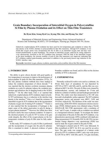
Grain Boundary Incorporation of Interstitial Oxygen in Polycrystalline ...
Grain Boundary Incorporation of Interstitial Oxygen in Polycrystalline ...
Grain Boundary Incorporation of Interstitial Oxygen in Polycrystalline ...

You also want an ePaper? Increase the reach of your titles
YUMPU automatically turns print PDFs into web optimized ePapers that Google loves.
Electronic Materials Letters, Vol. 4, No. 2 (2008), pp. 45-49<strong>Gra<strong>in</strong></strong> <strong>Boundary</strong> <strong>Incorporation</strong> <strong>of</strong> <strong>Interstitial</strong> <strong>Oxygen</strong> <strong>in</strong> Polycrystall<strong>in</strong>eSi Film by Plasma Oxidation and its Effect on Th<strong>in</strong> Film TransistorsBo Hyun Kim, Seung Ryul Lee, Kyung M<strong>in</strong> Ahn, and Byung Tae Ahn*Department <strong>of</strong> Materials Science and Eng<strong>in</strong>eer<strong>in</strong>g, Korea Advanced Institute <strong>of</strong>Science and Technology (KAIST), 335 Gwahangno, Yuseong-gu, Daejeon 305-701, KoreaInductively coupled plasma (ICP) oxidation has been used for low-temperature gate oxidation to reduce thetrap density at the Si/SiO 2 <strong>in</strong>terface <strong>in</strong> polycrystall<strong>in</strong>e-Si th<strong>in</strong> film transistors. Through ICP oxidation, it wasfound that oxygen atoms were <strong>in</strong>corporated <strong>in</strong>to the Si film as an <strong>in</strong>terstitial oxygen state and they werelocated predom<strong>in</strong>antly at gra<strong>in</strong> boundaries. The amount <strong>of</strong> <strong>in</strong>terstitial oxygen, analyzed by energy dispersivex-ray spectroscopy, <strong>in</strong>creased as the ICP oxidation time <strong>in</strong>creased. With the help <strong>of</strong> the <strong>in</strong>terstitial oxygenat the gra<strong>in</strong> boundaries, the electron mobility <strong>of</strong> poly-Si th<strong>in</strong> film transistors was improved, <strong>in</strong>dicat<strong>in</strong>g thatICP oxidation enabled gra<strong>in</strong>-boundary passivation <strong>in</strong> addition to the previously-known trap reduction at theSi/SiO 2 <strong>in</strong>terface state.Keywords: <strong>in</strong>terstitial oxygen, plasma oxydation, passivation, polycrystall<strong>in</strong>e silicon th<strong>in</strong> film transistor1. INTRODUCTIONThe ability to grow silicon dioxide with good quality atlow temperatures is necessary to improve the performance <strong>of</strong>polycrystall<strong>in</strong>e Si (poly-Si) th<strong>in</strong> film transistors (TFTs). Tothis end, plasma oxidation methods have been studied toreduce the oxidation temperature <strong>of</strong> silicon dioxide. [1-4] Itwas reported that the electron cyclotron resonance plasmaoxidation on a poly-Si substrate reduces the oxidation temperatureand m<strong>in</strong>imizes the Si dangl<strong>in</strong>g bonds at the Si/SiO 2<strong>in</strong>terface. [1,2] On the other hand, Choi et al. reported that<strong>in</strong>ductively coupled plasma (ICP) oxidation improved poly-Si TFT performance due to a reduction <strong>in</strong> the <strong>in</strong>terface trapdensity at the <strong>in</strong>terface. [3] Kim et al. found the existence <strong>of</strong><strong>in</strong>terstitial oxygen by ICP oxidation due to the <strong>in</strong>corporation<strong>of</strong> plasma oxygen <strong>in</strong>to Si dur<strong>in</strong>g ICP oxidation. [5,6] Nickel etal. also reported that the <strong>in</strong>corporation <strong>of</strong> hydrogen is themajor cause <strong>of</strong> the defect passivation <strong>in</strong> poly-Si dur<strong>in</strong>g aoxygen plasma treatment. [7,8] However, few efforts have beendevoted to clarify this issue <strong>in</strong> plasma oxidation. To improvethe electrical property <strong>of</strong> a poly-Si TFT <strong>in</strong> terms <strong>of</strong> its gateoxide <strong>in</strong>tegrity, the effect <strong>of</strong> the oxygen plasma on the lowtemperature oxidation <strong>of</strong> poly-Si film must be fully understood.In this study, ICP oxidation <strong>of</strong> a poly-Si film is performedand the <strong>in</strong>corporation <strong>of</strong> oxygen <strong>in</strong>to the poly-Si substratefilm is exam<strong>in</strong>ed <strong>in</strong> detail. A physical evidence <strong>of</strong> gra<strong>in</strong>*Correspond<strong>in</strong>g author: btahn@kaist.ac.krboundary oxidation was found, and its effect on the electronmobility <strong>of</strong> TFTs is discussed.2. EXPERIMENTALThermally oxidized Si wafers were used as a substrate. An84-nm thick layer <strong>of</strong> amorphous Si was deposited byLPCVD at 550°C with SiH 4 and H 2 , and the film was crystallizedat 600°C for 48 h. The poly-Si films were cleaned bytrichloroethylene, acetone, and methanol for 15 m<strong>in</strong> andboiled <strong>in</strong> a solution <strong>of</strong> sulfuric acid and hydrogen peroxide for20 m<strong>in</strong>. The wafers were then immersed <strong>in</strong> a 50:1 HF solutionuntil a hydrophobic surface appeared. The ICP oxidationtemperature, power, and pressure were 400°C, 2 kW, and10 mTorr, respectively. The thickness <strong>of</strong> the oxide was measuredus<strong>in</strong>g a JEM-3010 JEOL transmission electron microscopy(TEM). Infrared spectra were obta<strong>in</strong>ed us<strong>in</strong>g a NicoletMAGNA-IR 560 FTIR spectrometer with a resolution <strong>of</strong>4cm -1 and 32 scans. A sample with no oxidation was utilizedas a background reference sample. To <strong>in</strong>vestigate the chemicalcomposition <strong>of</strong> the poly-Si film after ICP oxidation, x-rayphotoelectron spectroscopy (XPS) comb<strong>in</strong>ed with depth pr<strong>of</strong>il<strong>in</strong>gmeasurement (VG Scientific ESCALAB 250) was performed.Energy dispersive x-ray spectroscopy (EDS) wasused to study the oxygen content <strong>in</strong> the poly-Si film.Self-aligned n-channel poly-Si TFTs were fabricated. Sifilm crystallized at 600°C for 48 h was used for an activelayer. The gate oxide was composed <strong>of</strong> a bottom oxidegrown by ICP O 2 oxidation at 400°C and a top oxide grownby LPCVD at 340°C with SiH 4 and O 2 . For gate electrodes,
46 B. H. Kim et al.: <strong>Gra<strong>in</strong></strong> <strong>Boundary</strong> <strong>Incorporation</strong> <strong>of</strong> <strong>Interstitial</strong> <strong>Oxygen</strong> <strong>in</strong> Polycrystall<strong>in</strong>e Si Filma 150-nm thick amorphous Si was deposited by PECVD at400°C with SiH 4 and was crystallized at 600°C for 48 h. Thegate and source/dra<strong>in</strong> regions were doped at 450°C us<strong>in</strong>g anion shower method with a dose <strong>of</strong> 2.2×10 16 cm -2 by H 2 -diluted PH 3 gas at an acceleration voltage <strong>of</strong> 10 kV. A 300-nm thick <strong>in</strong>terlayer oxide was deposited by LPCVD at340°C with SiH 4 and O 2 , and was annealed at 500°C for 30m<strong>in</strong> <strong>in</strong> N 2 . After open<strong>in</strong>g contact holes, a 500-nm thick Allayer was deposited by sputter<strong>in</strong>g and the layer was patterned.F<strong>in</strong>ally, the TFT samples were annealed at 450°C for30 m<strong>in</strong> <strong>in</strong> a 10% H 2 /N 2 gas. Electrical properties <strong>of</strong> the TFTswere measured us<strong>in</strong>g an HP 4145B semiconductor parameteranalyzer.film by ICP oxidation at 400°C. The oxidation times for 7.5,11.9 and 16.0-nm thick oxides were 10, 50, and 90 m<strong>in</strong>,respectively. The absorption spectra show the characteristics3. RESULTS AND DISCUSSIONFigure 1(a) shows the <strong>in</strong>frared absorption peaks <strong>of</strong> a SiO 2 /Si film with various oxide thicknesses grown on a poly-SiFig. 1. Infrared absorption spectra <strong>of</strong> (a) an ICP SiO 2/poly-Si filmwith various oxide thicknesses and (b) a poly-Si film after removal <strong>of</strong>the ICP oxide <strong>in</strong> a 50:1 HF solution.Fig. 2. XPS depth pr<strong>of</strong>ile <strong>of</strong> the (a) Si 2p and (b) O 1s peaks <strong>of</strong> apoly-Si film with a 16.0-nm thick ICP oxide, and (c) the enlarged O1s peak from (b) after sputter<strong>in</strong>g <strong>of</strong> 80 and 130 m<strong>in</strong>.Electron. Mater. Lett. Vol. 4, No. 2 (2008)
B. H. Kim et al.: <strong>Gra<strong>in</strong></strong> <strong>Boundary</strong> <strong>Incorporation</strong> <strong>of</strong> <strong>Interstitial</strong> <strong>Oxygen</strong> <strong>in</strong> Polycrystall<strong>in</strong>e Si Film 47<strong>of</strong> SiO 2 with stretch<strong>in</strong>g, bend<strong>in</strong>g, and rock<strong>in</strong>g bands locatedat 1100, 800, and 455 cm -1 , respectively. [9] Figure 1(b) showsthe <strong>in</strong>frared absorption peaks <strong>of</strong> the poly-Si film after etch<strong>in</strong>gaway the ICP oxide <strong>in</strong> a 50:1 HF solution until hydrophobiaappears. The absorption peaks do not exist on thepoly-Si film on which a 7.5-nm thick oxide was grown andetched away. However, the Si-O absorption peak appears onthe poly-Si film where 11.9-nm thick oxide was grown andremoved. The poly-Si film on which 16.0-nm thick oxidewas grown and removed shows clear Si-O bond<strong>in</strong>g characteristics,<strong>in</strong>clud<strong>in</strong>g Si-O stretch<strong>in</strong>g, bend<strong>in</strong>g, and rock<strong>in</strong>gbands. The results <strong>in</strong>dicate that oxygen exists <strong>in</strong> the poly-Sifilm and the amount <strong>of</strong> oxygen with<strong>in</strong> the film <strong>in</strong>creases asthe oxidation time <strong>in</strong>creases.Figure 2 shows the XPS depth pr<strong>of</strong>ile <strong>of</strong> the (a) Si 2p and(b) O 1s peaks from the SiO 2 /poly-Si film with 16.0-nmthick ICP oxide. In Fig. 2(a), two Si 2p peaks are clearlyseen: Si 4+ <strong>in</strong> the oxide layer and Si 0 <strong>in</strong> the poly-Si film. [10] Inthe beg<strong>in</strong>n<strong>in</strong>g, only the Si 4+ peak (104.4 eV) was evident.The Si 0 peak (99.3 eV) then appeared after 15-m<strong>in</strong> <strong>of</strong> sputter<strong>in</strong>g.The Si 4+ peak completely disappeared after 45-m<strong>in</strong> <strong>of</strong>sputter<strong>in</strong>g and only the Si 0 peak rema<strong>in</strong>ed. This <strong>in</strong>dicates thata sputter<strong>in</strong>g time <strong>of</strong> 45 m<strong>in</strong> completely removes the ICPoxide from the SiO 2 /poly-Si film. In Fig. 2(b), <strong>in</strong>itially, the O1s peak (534.0 eV) from SiO 2 is shown and then the peakgradually shifts to an <strong>in</strong>terstitial O 1s peak (531.5 eV). TheSiO 2 O 1s peak completely disappears after 45-m<strong>in</strong> <strong>of</strong> sputter<strong>in</strong>g.Figure 2(c) shows the enlarged O 1s peak with 80-and 130-m<strong>in</strong> sputter<strong>in</strong>g from Fig. 1. Here, the O 1s peak canstill be detected after 130-m<strong>in</strong> <strong>of</strong> sputter<strong>in</strong>g, whereas theSiO 2 layer on the poly-Si film is completely removed after45-m<strong>in</strong> <strong>of</strong> sputter<strong>in</strong>g, as shown <strong>in</strong> Figs. 2(a) and 2(b). Thisclearly demonstrates that <strong>in</strong>terstitial O atoms exist deep <strong>in</strong>the poly-Si film as well as on the surface <strong>of</strong> the film. Theoxygen content <strong>in</strong> the poly-Si film after 130-m<strong>in</strong> <strong>of</strong> sputter<strong>in</strong>gwas approximately 5.2 at% from the XPS analysis.To <strong>in</strong>vestigate the oxygen distribution with<strong>in</strong> the poly-Sifilm, TEM and EDS were utilized. Figure 3 shows a crosssectionalTEM micrograph <strong>of</strong> the poly-Si film on which (a)7.5-, (b) 11.9-, and (c) 16.0-nm thick ICP oxide were grownand removed. The areas with arrows are the sites where theEDS measurements were performed.Figure 4 shows the oxygen atomic contents <strong>in</strong>side thegra<strong>in</strong>s and at the gra<strong>in</strong> boundaries <strong>in</strong> the poly-Si film wherethe ICP oxides with various thicknesses were grown andremoved. The oxygen atomic contents <strong>in</strong> the poly-Si film, onwhich 16.0-nm thick ICP oxide was grown and removed,were 15.0 at% <strong>in</strong>side the gra<strong>in</strong>s and 33.7 at% at the gra<strong>in</strong>boundaries. The oxygen content measured by EDS is largerthan that measured by XPS (5.2 at %). As the beam size used<strong>in</strong> the EDS measurement was approximately 5 nm, the precisecontent at a specific po<strong>in</strong>t cannot be determ<strong>in</strong>ed. Thethermal SiO 2 below the poly-Si and the ICP oxide above thepoly-Si may have had a background effect on the oxygenatomic content <strong>in</strong> the poly-Si. However, a trend <strong>in</strong> the compositionaldifference between the gra<strong>in</strong>s and gra<strong>in</strong> boundariesis clearly seen. Given that no oxygen with<strong>in</strong> the gra<strong>in</strong>sis expected dur<strong>in</strong>g thermal oxidation, the oxygen detected byFig. 3. Cross-sectional TEM micrograph <strong>of</strong> a poly-Si on which (a)7.5-, (b) 11.9-, and (c) 16.0-nm thick ICP oxide was grown.Fig. 4. EDS analysis <strong>of</strong> the <strong>in</strong>terstitial oxygen content <strong>in</strong>side thegra<strong>in</strong>s and at the gra<strong>in</strong> boundaries <strong>in</strong> the poly-Si film where the ICPoxide was grown and removed as a function <strong>of</strong> the ICP oxide thickness.Electron. Mater. Lett. Vol. 4, No. 2 (2008)
48 B. H. Kim et al.: <strong>Gra<strong>in</strong></strong> <strong>Boundary</strong> <strong>Incorporation</strong> <strong>of</strong> <strong>Interstitial</strong> <strong>Oxygen</strong> <strong>in</strong> Polycrystall<strong>in</strong>e Si FilmFig. 5. Schematic diagram <strong>of</strong> <strong>in</strong>terstitial oxygen distribution <strong>in</strong> polycrystall<strong>in</strong>eSi film by plasma oxidation: The <strong>in</strong>terstitial oxygen contentis high at the gra<strong>in</strong> boundaries.XPS must have orig<strong>in</strong>ated from the oxygen at the gra<strong>in</strong>boundaries. The amount <strong>of</strong> oxygen at the gra<strong>in</strong> boundaries<strong>in</strong>creases as the oxidation time <strong>in</strong>creases. This result <strong>in</strong>dicatesthat the ma<strong>in</strong> route <strong>of</strong> oxygen <strong>in</strong>corporation <strong>in</strong> the poly-Si film is the gra<strong>in</strong> boundaries.Figure 5 shows a schematic diagram <strong>of</strong> oxygen <strong>in</strong>corporationby ICP oxidation. When the ICP oxidation time is long,the concentration <strong>of</strong> <strong>in</strong>terstitial oxygen is high at the gra<strong>in</strong>boundaries, whereas it is low when the oxidation time isshort. The <strong>in</strong>corporation <strong>of</strong> oxygen at the gra<strong>in</strong> boundaries isan important f<strong>in</strong>d<strong>in</strong>g <strong>in</strong> this paper.Figure 6 shows the dra<strong>in</strong> current and electron mobility versusthe gate voltage <strong>of</strong> the poly-Si TFTs with two differentgate oxides. One gate oxide was prepared by grow<strong>in</strong>g a 7.5-nm ICP oxide and a 72-nm LPCVD oxide (total 79.5 nm),and the second gate oxide was prepared by grow<strong>in</strong>g a 16.0-nm ICP oxide and a 68-nm LPCVD oxide (total 84 nm). TheICP oxide was grown at 400°C. The width and length <strong>of</strong> thetransistor are 10 and 10 µm, respectively, and the dra<strong>in</strong>sourcevoltage, V DS , is 3 V. The field effect mobility, µ FE ,was calculated from the transconductance. The maximumµ FE value <strong>of</strong> a TFT with a 7.5-nm thick ICP oxide is 11.4cm 2 /Vs, while that <strong>of</strong> a TFT with a 16.0-nm thick ICP oxideis 13.0 cm 2 /Vs. A TFT with a thicker ICP oxide and moreoxygen <strong>in</strong> the active layer shows a higher value <strong>of</strong> µ FE .The mobility <strong>of</strong> a poly-Si TFT is affected by surface scatter<strong>in</strong>gwith<strong>in</strong> the gra<strong>in</strong>s and by gra<strong>in</strong> boundary scatter<strong>in</strong>g.Accord<strong>in</strong>g to the thermionic emission model [11] , the dra<strong>in</strong>current, I D , is expressed byI D =(W/L)µ C ox (V G -V FB )V DS =(W/L)µ 0 exp(-qE B /kT)C ox (V G -V FB )V DS , (1)where W is the channel width, L is the channel length, µ 0 isthe carrier mobility with<strong>in</strong> each gra<strong>in</strong> and C ox is the gateoxide capacitance, respectively. The electron mobility term,µ, is divided <strong>in</strong>to µ 0 and exp(-qE B /kT). The second term isFig. 6. Log I D versus V G and electron mobility versus the V G characteristics<strong>of</strong> poly-Si TFTs with two different double-layer gate oxides:one with ICP oxide (7.5 nm)/ LPCVD oxide (72 nm) and the otherwith ICP oxide (16.0 nm)/ LPCVD oxide(68 nm).Fig. 7. Plot <strong>of</strong> ln[I D/(V G-V FB)V DS] versus 1/(V G-V FB) 2 <strong>of</strong> poly-Si TFTswith two different double-layer gate oxides: one with ICP oxide (7.5nm)/ LPCVD (72 nm) and the other with ICP oxide (16.0 nm )/LPCVD (68 nm).the energy barrier term at the gra<strong>in</strong> boundaries. The energybarrier, E B , and the thickness <strong>of</strong> the channel, t ch , areexpressed, respectively, asE B = q 2 N 2 T t ch /8ε Si C ox (V G -V FB ) (2)t ch = [8kTt ox (ε Si /ε SiO2 ) 0.5 ]/[q(V G -V FB )], (3)where ε Si and ε SiO2 are the permittivities <strong>of</strong> Si and SiO 2 ,Electron. Mater. Lett. Vol. 4, No. 2 (2008)