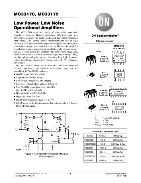
MC33178, MC33179 Low Power, Low Noise Operational ... - Intusoft
MC33178, MC33179 Low Power, Low Noise Operational ... - Intusoft
MC33178, MC33179 Low Power, Low Noise Operational ... - Intusoft

You also want an ePaper? Increase the reach of your titles
YUMPU automatically turns print PDFs into web optimized ePapers that Google loves.
<strong>MC33178</strong>, <strong>MC33179</strong>DC ELECTRICAL CHARACTERISTICS (V CC = +15 V, V EE = –15 V, T A = 25°C, unless otherwise noted.)Characteristics Figure Symbol Min Typ Max UnitInput Offset Voltage (R S = 50 Ω, V CM = 0 V, V O = 0 V)(V CC = +2.5 V, V EE = –2.5 V to V CC = +15 V, V EE = –15 V)T A = +25°CT A = –40° to +85°CAverage Temperature Coefficient of Input Offset Voltage(R S = 50 Ω, V CM = 0 V, V O = 0 V)T A = –40° to +85°CInput Bias Current (V CM = 0 V, V O = 0 V)T A = +25°CT A = –40° to +85°CInput Offset Current (V CM = 0 V, V O = 0 V)T A = +25°CT A = –40° to +85°CCommon Mode Input Voltage Range(∆V IO = 5.0 mV, V O = 0 V)Large Signal Voltage Gain (V O = –10 V to +10 V, R L = 600 Ω)T A = +25°CT A = –40° to +85°COutput Voltage Swing (V ID = ±1.0 V)(V CC = +15 V, V EE = –15 V)R L = 300 ΩR L = 300 ΩR L = 600 ΩR L = 600 ΩR L = 2.0 kΩR L = 2.0 kΩ(V CC = +2.5 V, V EE = –2.5 V)R L = 600 ΩR L = 600 Ω3 |V IO |3 ∆V IO /∆T––4, 5 I IB––|I IO |0.15–3.04.0– 2.0 –––6 V ICR –13–7, 8 A VOL50259, 10, 11V O +V O –V O +V O –V O +V O –V O +V O –––+12–+13–1.1–100–5.0––14+14200–+12–12+13.6–13+14–13.8Common Mode Rejection (V in = ±13 V) 12 CMR 80 110 – dB<strong>Power</strong> Supply RejectionV CC /V EE = +15 V/ –15 V, +5.0 V/ –15 V, +15 V/ –5.0 VOutput Short Circuit Current (V ID = ±1.0 V, Output to Ground)Source (V CC = 2.5 V to 15 V)Sink (V EE = –2.5 V to –15 V)<strong>Power</strong> Supply Current (V O = 0 V)(V CC = 2.5 V, V EE = –2.5 V to V CC = +15 V, V EE = –15 V)<strong>MC33178</strong> (Dual)T A = +25°CT A = –40° to +85°C<strong>MC33179</strong> (Quad)T A = +25°CT A = –40° to +85°C13 PSR14, 15 I SC+50–5016 I D––1.6–1.65006005060–+13––––––12––13––1.180 110 –––+80–100––1.7–––1.41.62.42.6mVµV/°CnAnAVkV/VVdBmAmAhttp://onsemi.com3
<strong>MC33178</strong>, <strong>MC33179</strong>AC ELECTRICAL CHARACTERISTICS (V CC = +15 V, V EE = –15 V, T A = 25°C, unless otherwise noted.)Characteristics Figure Symbol Min Typ Max UnitSlew Rate17, 32 SRV/µs(V in = –10 V to +10 V, R L = 2.0 kΩ, C L = 100 pF, A V = +1.0 V)1.2 2.0 –Gain Bandwidth Product (f = 100 kHz) 18 GBW 2.5 5.0 – MHzAC Voltage Gain (R L = 600 Ω, V O = 0 V, f = 20 kHz) 19, 20 A VO – 50 – dBUnity Gain Bandwidth (Open–Loop) (R L = 600 Ω, C L = 0 pF) BW – 3.0 – MHzGain Margin (R L = 600 Ω, C L = 0 pF) 21, 23, 24 A m – 15 – dBPhase Margin (R L = 600 Ω, C L = 0 pF) 22, 23, 24 φ m – 60 – DegChannel Separation (f = 100 Hz to 20 kHz) 25 CS – –120 – dB<strong>Power</strong> Bandwidth (V O = 20 V pp, R L = 600 Ω, THD ≤ 1.0%) BW p – 32 – kHzTotal Harmonic Distortion (R L = 600 Ω,, V O = 2.0 V pp , A V = +1.0 V)(f = 1.0 kHz)(f = 10 kHz)(f = 20 kHz)26 THD–––0.00240.0140.024–––%Open Loop Output Impedance(V O = 0 V, f = 3.0 MHz, A V = 10 V)27 |Z O |– 150 –ΩDifferential Input Resistance (V CM = 0 V) R in – 200 – kΩDifferential Input Capacitance (V CM = 0 V) C in – 10 – pFEquivalent Input <strong>Noise</strong> Voltage (R S = 100 Ω,)f = 10 Hzf = 1.0 kHz28 e n––8.07.5––nV/ √HzEquivalent Input <strong>Noise</strong> Currentf = 10 Hzf = 1.0 kHz29 i n––0.330.15––pA/ √Hz ° ° Ω Figure 2. Maximum <strong>Power</strong> Dissipationversus TemperatureFigure 3. Input Offset Voltage versusTemperature for 3 Typical Unitshttp://onsemi.com4
<strong>MC33178</strong>, <strong>MC33179</strong> ° °Figure 4. Input Bias Currentversus Common Mode VoltageFigure 5. Input Bias Currentversus Temperature ° ∆ Figure 6. Input Common Mode VoltageRange versus Temperature ∆ Ω °Figure 7. Open Loop Voltage Gainversus Temperature Ω Ω, Ω Ω °φ ° Ω Ω Figure 8. Voltage Gain and Phaseversus FrequencyFigure 9. Output Voltage Swingversus Supply Voltagehttp://onsemi.com5
<strong>MC33178</strong>, <strong>MC33179</strong> ° ° ° ° ±Figure 10. Output Saturation Voltageversus Load Current Ω ≤ ° Figure 11. Output Voltageversus Frequency∆ ∆ ∆ ± °°∆ ∆ Figure 12. Common Mode Rejectionversus Frequency Over Temperature ∆ ∆ ∆ °° ∆ ± Figure 13. <strong>Power</strong> Supply Rejectionversus Frequency Over Temperature ± Figure 14. Output Short Circuit Currentversus Output Voltage ° ± Ω Figure 15. Output Short Circuit Currentversus Temperaturehttp://onsemi.com6
<strong>MC33178</strong>, <strong>MC33179</strong> µ ° ° ° Figure 16. Supply Current versus SupplyVoltage with No Load ∆ ∆ °Figure 17. Normalized Slew Rateversus TemperatureΩ Ω °Figure 18. Gain Bandwidth Productversus Temperature Ω ° Figure 19. Voltage Gain and Phaseversus Frequencyφ ° ∞ Figure 20. Voltage Gain and Phaseversus Frequencyφ Ω ° Figure 21. Open Loop Gain Marginversus Temperaturehttp://onsemi.com7
<strong>MC33178</strong>, <strong>MC33179</strong>φ Ω °Figure 22. Phase Marginversus Temperature ° ΩFigure 23. Phase Margin and Gain Marginversus Differential Source Resistanceφ Ω Figure 24. Open Loop Gain Margin and PhaseMargin versus Output Load Capacitanceφ Figure 25. Channel Separationversus Frequency Ω ° ° Ω Figure 26. Total Harmonic Distortionversus Frequency Ω Figure 27. Output Impedanceversus Frequency °http://onsemi.com8
<strong>MC33178</strong>, <strong>MC33179</strong> nV/ √ Hz ° pA/ √ Hz ° Ω Figure 28. Input Referred <strong>Noise</strong> Voltageversus FrequencyFigure 29. Input Referred <strong>Noise</strong> Currentversus Frequency ° Ω Figure 30. Percent Overshoot versusLoad Capacitance Ω ° Ω Ω °µFigure 31. Non–inverting Amplifier Slew Rate Ω °Figure 32. Small Signal Transient ResponseµFigure 33. Large Signal Transient Responsehttp://onsemi.com9
<strong>MC33178</strong>, <strong>MC33179</strong>PACKAGE DIMENSIONSPDIP–8P SUFFIXCASE 626–05ISSUE L–B– NOTE 2–T–HF–A–GCND K LJM SO–8D SUFFIXCASE 751–07ISSUE W–X–B–Y––Z–HGADSC N X 45MKJ http://onsemi.com12
<strong>MC33178</strong>, <strong>MC33179</strong>PACKAGE DIMENSIONSPDIP–14P SUFFIXCASE 646–06ISSUE MB –T–NA FL C K J H G D 14 PLM SO–14D SUFFIXCASE 751A–03ISSUE F–A––B–P 7 PL –T–GD 14 PL K C R X 45 F MJ http://onsemi.com13
<strong>MC33178</strong>, <strong>MC33179</strong>Noteshttp://onsemi.com14
<strong>MC33178</strong>, <strong>MC33179</strong>Noteshttp://onsemi.com15
<strong>MC33178</strong>, <strong>MC33179</strong>ON Semiconductor and are trademarks of Semiconductor Components Industries, LLC (SCILLC). SCILLC reserves the right to make changeswithout further notice to any products herein. SCILLC makes no warranty, representation or guarantee regarding the suitability of its products for any particularpurpose, nor does SCILLC assume any liability arising out of the application or use of any product or circuit, and specifically disclaims any and all liability,including without limitation special, consequential or incidental damages. “Typical” parameters which may be provided in SCILLC data sheets and/orspecifications can and do vary in different applications and actual performance may vary over time. All operating parameters, including “Typicals” must bevalidated for each customer application by customer’s technical experts. SCILLC does not convey any license under its patent rights nor the rights of others.SCILLC products are not designed, intended, or authorized for use as components in systems intended for surgical implant into the body, or other applicationsintended to support or sustain life, or for any other application in which the failure of the SCILLC product could create a situation where personal injury ordeath may occur. Should Buyer purchase or use SCILLC products for any such unintended or unauthorized application, Buyer shall indemnify and holdSCILLC and its officers, employees, subsidiaries, affiliates, and distributors harmless against all claims, costs, damages, and expenses, and reasonableattorney fees arising out of, directly or indirectly, any claim of personal injury or death associated with such unintended or unauthorized use, even if such claimalleges that SCILLC was negligent regarding the design or manufacture of the part. SCILLC is an Equal Opportunity/Affirmative Action Employer.PUBLICATION ORDERING INFORMATIONLiterature Fulfillment:Literature Distribution Center for ON SemiconductorP.O. Box 5163, Denver, Colorado 80217 USAPhone: 303–675–2175 or 800–344–3860 Toll Free USA/CanadaFax: 303–675–2176 or 800–344–3867 Toll Free USA/CanadaEmail: ONlit@hibbertco.comN. American Technical Support: 800–282–9855 Toll Free USA/CanadaJAPAN: ON Semiconductor, Japan Customer Focus Center4–32–1 Nishi–Gotanda, Shinagawa–ku, Tokyo, Japan 141–0031Phone: 81–3–5740–2700Email: r14525@onsemi.comON Semiconductor Website: http://onsemi.comFor additional information, please contact your localSales Representative.http://onsemi.com16<strong>MC33178</strong>/D