Conversion Efficiency Optimization of Cryogenically ... - nLIGHT
Conversion Efficiency Optimization of Cryogenically ... - nLIGHT
Conversion Efficiency Optimization of Cryogenically ... - nLIGHT
Create successful ePaper yourself
Turn your PDF publications into a flip-book with our unique Google optimized e-Paper software.
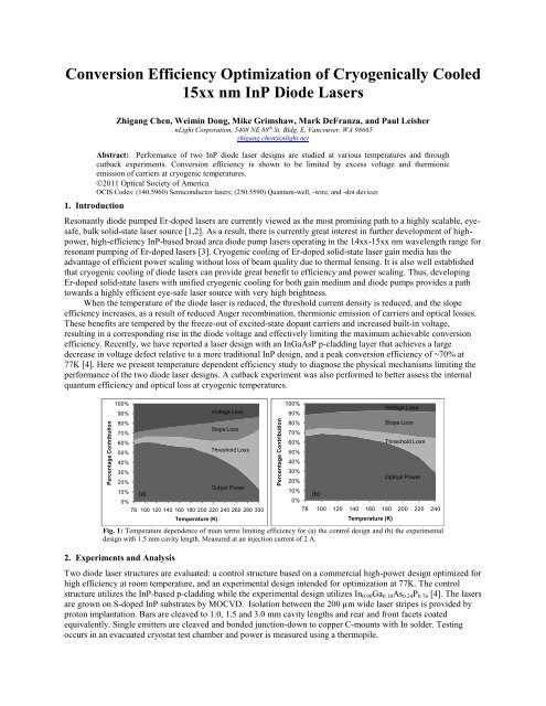
Percentage ContributionPercentage Contribution<strong>Conversion</strong> <strong>Efficiency</strong> <strong>Optimization</strong> <strong>of</strong> <strong>Cryogenically</strong> Cooled15xx nm InP Diode Lasers1. IntroductionZhigang Chen, Weimin Dong, Mike Grimshaw, Mark DeFranza, and Paul LeishernLight Corporation, 5408 NE 88 th St. Bldg. E, Vancouver, WA 98665zhigang.chen@nlight.netAbstract: Performance <strong>of</strong> two InP diode laser designs are studied at various temperatures and throughcutback experiments. <strong>Conversion</strong> efficiency is shown to be limited by excess voltage and thermionicemission <strong>of</strong> carriers at cryogenic temperatures.2011 Optical Society <strong>of</strong> AmericaOCIS Codes: (140.5960) Semiconductor lasers; (250.5590) Quantum-well, -wire, and -dot devicesResonantly diode pumped Er-doped lasers are currently viewed as the most promising path to a highly scalable, eyesafe,bulk solid-state laser source [1,2]. As a result, there is currently great interest in further development <strong>of</strong> highpower,high-efficiency InP-based broad area diode pump lasers operating in the 14xx-15xx nm wavelength range forresonant pumping <strong>of</strong> Er-doped lasers [3]. Cryogenic cooling <strong>of</strong> Er-doped solid-state laser gain media has theadvantage <strong>of</strong> efficient power scaling without loss <strong>of</strong> beam quality due to thermal lensing. It is also well establishedthat cryogenic cooling <strong>of</strong> diode lasers can provide great benefit to efficiency and power scaling. Thus, developingEr-doped solid-state lasers with unified cryogenic cooling for both gain medium and diode pumps provides a pathtowards a highly efficient eye-safe laser source with very high brightness.When the temperature <strong>of</strong> the diode laser is reduced, the threshold current density is reduced, and the slopeefficiency increases, as a result <strong>of</strong> reduced Auger recombination, thermionic emission <strong>of</strong> carriers and optical losses.These benefits are tempered by the freeze-out <strong>of</strong> excited-state dopant carriers and increased built-in voltage,resulting in a corresponding rise in the diode voltage and effectively limiting the maximum achievable conversionefficiency. Recently, we have reported a laser design with an InGaAsP p-cladding layer that achieves a largedecrease in voltage defect relative to a more traditional InP design, and a peak conversion efficiency <strong>of</strong> ~70% at77K [4]. Here we present temperature dependent efficiency study to diagnose the physical mechanisms limiting theperformance <strong>of</strong> the two diode laser designs. A cutback experiment was also performed to better assess the internalquantum efficiency and optical loss at cryogenic temperatures.100%90%80%70%60%50%40%30%20%10%0%(a)78 100 120 140 160 180 200 220 240 260 280 300Temperature (K)Voltage LossSlope LossThreshold LossOutput Power100%90%80%70%60%50%40%30%20%10%0%(b)78 100 120 140 160 180 200 220 240Temperature (K)Voltage LossSlope LossThreshold LossOptical PowerFig. 1: Temperature dependence <strong>of</strong> main terms limiting efficiency for (a) the control design and (b) the experimentaldesign with 1.5 mm cavity length. Measured at an injection current <strong>of</strong> 2 A.2. Experiments and AnalysisTwo diode laser structures are evaluated: a control structure based on a commercial high-power design optimized forhigh efficiency at room temperature, and an experimental design intended for optimization at 77K. The controlstructure utilizes the InP-based p-cladding while the experimental design utilizes In 0.90 Ga 0.10 As 0.24 P 0.76 [4]. The lasersare grown on S-doped InP substrates by MOCVD. Isolation between the 200 µm wide laser stripes is provided byproton implantation. Bars are cleaved to 1.0, 1.5 and 3.0 mm cavity lengths and rear and front facets coatedequivalently. Single emitters are cleaved and bonded junction-down to copper C-mounts with In solder. Testingoccurs in an evacuated cryostat test chamber and power is measured using a thermopile.
Internal quantum efficiencyoptical loss (1/cm)Internal quantum efficiencyoptical loss (1/cm)The relative contribution <strong>of</strong> main terms limiting efficiency can be represented by their percentage contributionto the injected electrical power. Fig. 1(a) illustrates these terms in the control design at various temperatures. Asshown, at cryogenic temperatures, slope loss and threshold current is greatly reduced, due to a dramatic reduction innon-radiative losses such as Shockley-Read-Hall and Auger recombination, as well as reduction in leakage currentassociated with thermionic emission <strong>of</strong> carriers from the quantum wells (QWs). However, the voltage defect (excessdiode voltage drop beyond photon voltage) is greatly increased at low temperatures, affecting the overall conversionefficiency. The experimental design features a reduction <strong>of</strong> voltage defect at cryogenic temperature throughincreasing doping density, reducing the energy band <strong>of</strong>fsets at the heterobarriers, and changing p-cladding materialsto reduce dopant ionization energy. The improved voltage loss is shown in Fig. 1(b), reduced from 30% in thecontrol design to ~10% in the experimental design. However, the slope loss remains relative large at cryogenictemperatures, mitigating the conversion efficiency gain through voltage improvement.110%100%90%80%70%60%50%(a)50 100 150 200 250 300Temperature (K)4.03.53.02.52.01.51.00.50.085%80%75%70%65%60%55%60 80 100 120 140 160 180 200 220Temperature (K)Fig. 2: Internal quantum efficiency ( i) and optical loss ( i) as a function <strong>of</strong> temperature for (a) control design and (b)experimental design, retrieved from cutback experiments.External differential efficiency D <strong>of</strong> the laser diode is related the internal quantum efficiency i and losses. Itcan be expressed in terms <strong>of</strong> D = i m /( m + i ), with m =ln(1/R 1 R 2 )/2L the mirror loss and i the internal opticalloss. i and i can be determined from the linear fit to inverse D versus cavity length L (so called cutback study).The extracted i and i at various temperatures are plotted in Fig. 2 for both the control and experimental designs. i<strong>of</strong> the control design tends toward 100% at low temperatures, indicating a total suppression <strong>of</strong> leakage current. Thelarge value <strong>of</strong> optical loss (>3 cm -1 ) at room temperature is probably due to strong intervalence band absorption(IVBA) at QWs and optical waveguide. If a temperature-independent absorption coefficient is assumed [5], IVBAshould be proportional to the free hole density, which follows Fermi function over temperature. The optical loss inFig. 2(a) qualitatively follows such dependence, until saturates at low temperatures at losses related to the scatteringloss and free carrier absorption within QWs. The optical loss in the experimental design has similar values to thosein the control design at low temperatures [Fig. 2(b)], excluding it as the limiting factor to conversion efficiency.However, the internal quantum efficiency is below 80% even at 77K, indicating non-vanishing leakage currentassociated with thermionic emission <strong>of</strong> carriers. This is probably related to reduced band <strong>of</strong>fset, as well as shallowQWs in the experimental design. A further improvement to the design <strong>of</strong> laser structure including the active regionand waveguide could result in further optimization <strong>of</strong> the overall conversion efficiency.3. ConclusionIn summary, the performance <strong>of</strong> two InP diode laser designs, optimized for room temperature and cryogenictemperatures, respectively, are studied at various temperatures. Analysis <strong>of</strong> the test data reveals how the major termslimiting efficiency evolve over temperature. Internal quantum efficiency and optical loss extracted from cutbackstudy provide further information on conversion efficiency, limited by excess diode voltage and thermionic emission<strong>of</strong> carriers at cryogenic temperatures, indicating opportunities for further efficiency improvement.4. References[1] S. Setzler, M. Francis, Y. Young, J. Konves, and E. Chicklis, IEEE J. Sel. Top. Quant. Electron., 11, 645-657 (2005).[2] D. Garbuzov, I. Kudryashov, and M. Dubinskii, Appl. Phys. Lett., 87, 121101, (2005).[3] M. Osowski, Y. Gewirtz, R. Lammert, S. Oh, C. Panja, V. Elarde, L. Vaissie, F. Patel, and J. Ungar, Proc. SPIE, 7325, 29, (2009).[4] P. Leisher, W. Dong, M. Grimshaw, M. DeFranza, M. Dubinskii, and S. Patterson, IEEE Photon. Technol. Lett., 22, 1829-1831 (2010).[5] C. Henry, R.Logan, F. Merritt, and J. Luongo, IEEE J. Quant. Electron., 19, 947-952 (1983).(b)1.41.31.21.11.00.90.80.70.60.50.4


