STM - Boulder School for Condensed Matter and Materials Physics
STM - Boulder School for Condensed Matter and Materials Physics
STM - Boulder School for Condensed Matter and Materials Physics
- No tags were found...

Create successful ePaper yourself
Turn your PDF publications into a flip-book with our unique Google optimized e-Paper software.
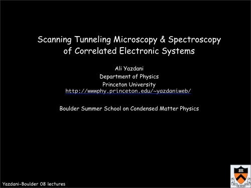
Scanning Tunneling Microscopy & Spectroscopyof Correlated Electronic SystemsAli YazdaniDepartment of <strong>Physics</strong>Princeton Universityhttp://wwwphy.princeton.edu/~yazdaniweb/<strong>Boulder</strong> Summer <strong>School</strong> on <strong>Condensed</strong> <strong>Matter</strong> <strong>Physics</strong>Yazdani-<strong>Boulder</strong> 08 lectures
Why do we need local measurements?• Conventional wisdom in solid state physics: b<strong>and</strong> theory• Past: Underst<strong>and</strong>ing things in momentum space is enough!• New wisdom?: <strong>for</strong> correlated or nanoscale systems this may not be enoughExamples:• R<strong>and</strong>omly doped systems are not spatially homogenous• Systems close to a transition may segregate in to different phases(ex: last conducting link in a metal-insulator transition)• Can learn about correlated system by study of their response to defects (impurities,vortices, boundaries)• “Fluctuating order”--search <strong>for</strong> “propensity” <strong>for</strong> organization of electrons• Complimenting spatially average measurements is also criticalYazdani-<strong>Boulder</strong> 08 lectures
Length Scales:• Inter-atomic distances: few Å• Electron wavelength: depending on density; “good metals” few Å, “Unconventionalmetals” about 10-15 Å, semiconductors 100-200 Å• Correlation lengths: conventional superconductors 100-1000 Å; unconventional onebelow 20 typically (size of a vortex or a defect state)• “Phase separation lengths”: depends on the model from 10s of Å to 1000 ÅYazdani-<strong>Boulder</strong> 08 lectures
Plan <strong>for</strong> LecturesLecture I• Brief history of tunneling: tunneling through insulating barriers• Basics of scanning tunneling microscopy• Some comments on construction of an <strong>STM</strong>• <strong>STM</strong> on simple metals--quantum interference of electronic states• <strong>STM</strong> on semiconductors--imaging <strong>and</strong> probing single dopants• <strong>STM</strong> on conventional superconductors--impurity effects in a BCS superconductorLecture II• <strong>STM</strong> on high-Tc superconductors• Local signatures of d-wave pairing• Quasi-particle Interference• Local Pairing above Tc <strong>and</strong> the phase diagram• Clues on the mechanism: electron-boson or not?Yazdani-<strong>Boulder</strong> 08 lectures
Leo EsakiIvar GiaeverShared Nobel Prize in <strong>Physics</strong>(with B. Josephson 1973)Yazdani-<strong>Boulder</strong> 08 lectures
Giaever Tunneling: Aluminum-oxide the key to tunneling1963Yazdani-<strong>Boulder</strong> 08 lectures
Giaever Tunneling: Aluminum-oxide the key to tunnelingPinhole free tunnel barrierYazdani-<strong>Boulder</strong> 08 lectures
Giaever Tunneling: Tunneling into a superconductorYazdani-<strong>Boulder</strong> 08 lectures
Giaever Tunneling: Tunneling into a superconductor (1963)Yazdani-<strong>Boulder</strong> 08 lecturesAl-AlOx-Pb junction: Pb goes superconducting at 7.2K
Basics of Tunneling• Giaever tunneling: conducting electrodes separated by an insulating barrier• Apply a voltage bias across the barrier to get a net tunneling current I• First consider elastic tunneling: electrons get across without change in E• Tunneling current depends on density of states (DOS) of the electrodes• If one of the electrodes has a simple DOS, we can use this technique to measurethe unknown DOS. (Except can not <strong>for</strong>get the influence of T)I(V, r ! ) = 4" 2" dE M(E) # tip(E) f (E)# 2 sample(E $ eV, r !++ %)(1$ f (E $ eV )) (, '$# tip(E)(1$ f (E))# sample(E $ eV, r ! *$+ &) f (E $ eV ))M 2 "e #z / z 0!Yazdani-<strong>Boulder</strong> 08 lecturesVery low T limit
Basics of Tunneling• Giaever tunneling: conducting electrodes separated by an insulating barrier• Apply a voltage bias across the barrier to get a net tunneling current I• First consider elastic tunneling: electrons get across without change in E• Tunneling current depends on density of states (DOS) of the electrodes• If one of the electrodes has a simple DOS, we can use this technique to measurethe unknown DOS. (Except can not <strong>for</strong>get the influence of T)I(V, r ! ) = 4" 2" dE M(E) # tip(E) f (E)# 2 sample(E $ eV, r !++ %)(1$ f (E $ eV )) (, '$# tip(E)(1$ f (E))# sample(E $ eV, r ! *$+ &) f (E $ eV ))M 2 "e #z / z 0I(V, ! r ) = 4" 2"+%&$%dE M(E) 2 # tip(E)# sample(E $ eV, ! r ) f (E) $ f (E $ eV )( )!Yazdani-<strong>Boulder</strong> 08 lecturesVery low T limit
Basics of Tunneling• Giaever tunneling: conducting electrodes separated by an insulating barrier• Apply a voltage bias across the barrier to get a net tunneling current I• First consider elastic tunneling: electrons get across without change in E• Tunneling current depends on density of states (DOS) of the electrodes• If one of the electrodes has a simple DOS, we can use this technique to measurethe unknown DOS. (Except can not <strong>for</strong>get the influence of T)I(V, r ! ) = 4" 2" dE M(E) # tip(E) f (E)# 2 sample(E $ eV, r !++ %)(1$ f (E $ eV )) (, '$# tip(E)(1$ f (E))# sample(E $ eV, r ! *$+ &) f (E $ eV ))M 2 "e #z / z 0I(V, ! r ) = 4" 2"+%&$%dE M(E) 2 # tip(E)# sample(E $ eV, ! r ) f (E) $ f (E $ eV )( )E F +V%I(V, r ! ) " M 2 dE# tip(E)# sample(E F$ eV, r ! )E F!Yazdani-<strong>Boulder</strong> 08 lecturesVery low T limit
Principles of Tunneling SpectroscopyA la J. Bardeen, Phys. Rev. Lett. 6, 57 (1960).E F +V%I(V, r ! ) " M 2 # tipdE# sample(E F$ eV, r ! )E F!In the limit of low temperature, theFermi functions can be replaced by stepfunctions. If the tip DOS <strong>and</strong> thetunneling matrix M are constant in theenergy range of interest, then thisexpression reduces to:dI(V,! dVr ) " M 2 # tip# sample(E F$ eV, r ! )So far consider elastic tunneling only!Yazdani-<strong>Boulder</strong> 08 lectures!
Vacuum Tunneling: Binning & Rohrer (IBM-1980)• Tunneling exponential with distance• In vacuum: order of magnitude I/Angstrom• With a tip per<strong>for</strong>m local tunneling• First idea was to do local spectroscopy• Imaging was a secondary realizationYazdani-<strong>Boulder</strong> 08 lectures
Yazdani-<strong>Boulder</strong> 08 lectures
Yazdani-<strong>Boulder</strong> 08 lecturesThe First Scanning Tunneling Microscope
Commonly used piezo-electric element <strong>for</strong> an <strong>STM</strong> ScanHeadYazdani-<strong>Boulder</strong> 08 lectures
Various Coarse Approach MechanismPan WalkerBesoke/Bettle WalkerYazdani-<strong>Boulder</strong> 08 lectures
TipBasics of <strong>STM</strong>:Vacuum• Tunnel not from a macroscopic electrode butfrom a sharp tip• The barrier is vacuum• Since tunneling is exponential in distance--allcurrent happens with a tunneling cone under thetipcurrentSurface• If the tip is sharp, the spatial extent isroughly the height of the tip• Typical condition: 5-6 Å, 1V, you get a 1 nano-Amp of current (easy to measure with room tempelectrometer)Yazdani-<strong>Boulder</strong> 08 lectures
Block Diagram of an <strong>STM</strong>VibrationIsolationCurrentAmplifierSampleTipPiezoVoltageControlledEnvironmentBiasVoltageSystemControlYazdani-<strong>Boulder</strong> 08 lectures
Basics II: <strong>STM</strong> topography• The most typical use of the <strong>STM</strong> is to record a constant current image• A feedback loop adjusts the height of the tip to keep I constant• As another circuit scans the tip across an area (typically 100 Å)• Computer record <strong>and</strong> displays the trajectory of the tip• Constant-I topograph is a map of contours of constant DOS in vacuumTipTipVacuumTip Trajectory <strong>for</strong>constant currentcurrentSurfaceYazdani-<strong>Boulder</strong> 08 lectures
Atomic Scale Imaging with <strong>STM</strong>• Binning & Rohrer realized how local tunneling can be usedas an atomic scale imaging tool• First example: Si 7X7 surface reconstructionFirst “<strong>STM</strong> Topograph”--Binning& Rohrer 1983Si (111) SurfaceYazdani-<strong>Boulder</strong> 08 lectures
Yazdani-<strong>Boulder</strong> 08 lecturesRohrer & BinnigIBM Lab in ZurichInvented <strong>STM</strong> in 1981Nobel Prize awarded 1986
Construction of an <strong>STM</strong>• Scanning with piezoelectric elements: 1A/V• Tips: “hard” metals such as W, Pt, Ir• Coarse (mm range) <strong>and</strong> fine motion (0.1um range) are separate• Need clean surfaces: UHV environment (10 -6 Torr about 1 monolayer/sec)• Need low vibrations: floating table, rigid construction, acoustic rooms• Need low electrical noise: Rf shielding, low noise high voltage amplification• Need to measure small currents: Large gain, low noise, electrometers• Most important of all you need the sample surface to cooperate!• It can be a pain to make all these work at the same time!Yazdani-<strong>Boulder</strong> 08 lectures
Scanning Tunneling Microscopy Laboratory:(1.5K
The schematic of a UHV low temperature <strong>STM</strong>Load LockSputter GunAugerMass SpectrometerScanner AssemblyEvaporatorVibrationIsolationLEEDOpticalTableMicroscopeLiquid Helium DeWar <strong>and</strong>10 Tesla MagnetVacuum PumpsYazdani-<strong>Boulder</strong> 08 lectures
The schematic of a Variable Temperature UHV <strong>STM</strong> systemVacuum PumpsYazdani-<strong>Boulder</strong> 08 lectures
VT-<strong>STM</strong> HeadDesigned <strong>for</strong> highertemperatures• Thermal compensation• Compact design• Result :• Extremely low drift athightemperaturesYazdani-<strong>Boulder</strong> 08 lectures
Trouble with a movable vacuum tunnel junction:Yazdani-<strong>Boulder</strong> 08 lectures
Princeton Nanoscale Microscopy Lab:• Floating 30T slab of concrete supporting an acoustic/rf enclosure• For operation high resolution scanning probe microscopes• Outcome: better than 30ng of floor vibrationYazdani-<strong>Boulder</strong> 08lectures
<strong>STM</strong> on Simple MetalsElectron Waves & QuantumInterferenceYazdani-<strong>Boulder</strong> 08 lectures
Electron Waves:Surface waves onnoble metal surfaceCu(111)1000Å x 1000ÅYazdani-<strong>Boulder</strong> 08 lectures
Substrate: Au(111) on MicaReconstructedSurface &adsorbatesYazdani-<strong>Boulder</strong> 08 lecturesConstant current image, V=100 mV, I=90 pA1000 Å x 1000 Å
Simple Examples of Spectroscopy• Surface state on noble metal surfaces (Au, Cu, Ag);where bulk states are <strong>for</strong>bidden• Au(111) surface has a two-dimensional surface state• Measured previously with photoemission• <strong>STM</strong> spectroscopy can probe these statesBulk b<strong>and</strong> structureYazdani-<strong>Boulder</strong> 08 lectures
Yazdani-<strong>Boulder</strong> 08 lecturesScattering from chemical impurities
St<strong>and</strong>ing Waves in Simple Metals• Scattering from step edges <strong>and</strong> defect creates a situation <strong>for</strong> wave interference• At each energy electrons have different wavelength <strong>and</strong> hence a satisfy slightlydifferent interference conditiondI/dV maps Ag(111)500Å x 500ÅYazdani-<strong>Boulder</strong> 08 lectures500Å x 500Å
St<strong>and</strong>ing Waves in Simple Metals• Scattering from step edges <strong>and</strong> defect creates a situation <strong>for</strong> wave interference• At each energy electrons have different wavelength <strong>and</strong> hence a satisfy slightlydifferent interference conditiondI/dV maps Ag(111)500Å x 500ÅYazdani-<strong>Boulder</strong> 08 lectures500Å x 500Å
St<strong>and</strong>ing Waves in Simple Metals• Elastic scattering electron from k 1 to k 2allows mapping the Fermi Surface• A st<strong>and</strong>ing wave occur with Q=k1 - k2• At different energies different Q’sFourier Trans<strong>for</strong>m of the dI/dV maps Ag(111)<strong>STM</strong> & ARPES E(!) <strong>for</strong>Au111Yazdani-<strong>Boulder</strong> 08 lectures
St<strong>and</strong>ing Waves in Simple Metals• Elastic scattering electron from k 1 to k 2allows mapping the Fermi Surface• A st<strong>and</strong>ing wave occur with Q=k1 - k2• At different energies different Q’sFourier Trans<strong>for</strong>m of the dI/dV maps Ag(111)<strong>STM</strong> & ARPES E(!) <strong>for</strong>Au111Yazdani-<strong>Boulder</strong> 08 lectures
Scattering of Electrons from a Hard WallYazdani-<strong>Boulder</strong> 08 lectures
Yazdani-<strong>Boulder</strong> 08 lectures
Particle in a boxSurface waves : states that decay into the bulk of the sampleAdsorbates at 4K can be used to confine these states into artificial boxesYazdani-<strong>Boulder</strong> 08 lecturesExample: Iron atom corrals onCu(111) Crommie <strong>and</strong> Eigler1992-3
Spectroscopy Fabrication of of a device: particle Quantum in a box Corrals statesIron atom corrals on Cu(111)Yazdani-<strong>Boulder</strong> 08 lecturesCrommie <strong>and</strong> Eigler- 1992-93Particle in a box states.Complete description by two quantum numbers
Spectroscopy Fabrication of of a device: particle Quantum in a box Corrals statesIron atom corrals on Cu(111)Yazdani-<strong>Boulder</strong> 08 lecturesCrommie <strong>and</strong> Eigler- 1992-93Particle in a box states.Complete description by two quantum numbers
<strong>STM</strong> on SemiconductorsImaging Single DopantsYazdani-<strong>Boulder</strong> 08 lectures
<strong>STM</strong> on GaAs (110) surface•Easily cleaved (110) surface—exposed in UHV•Simple buckling of the surface bonds•Ga or As atoms via empty or filled states•<strong>STM</strong> can be used to image individual acceptors &donorsGa atoms on GaAs surfaceEmpty states, +1.6V100Å x 100Å[1-10][001]AsGa
<strong>STM</strong> on GaAs (110) surface•Easily cleaved (110) surface—exposed in UHV•Simple buckling of the surface bonds•Ga or As atoms via empty or filled states•<strong>STM</strong> can be used to image individual acceptors &donorsGa atoms on GaAs surfaceEmpty states, +1.6V100Å x 100Å[1-10][001]AsGaAs atoms on GaAs surfaceFilled States, -1.6V100Å x 100Å
<strong>STM</strong> on GaAs (110) surface•Easily cleaved (110) surface—exposed in UHV•Simple buckling of the surface bonds•Ga or As atoms via empty or filled states•<strong>STM</strong> can be used to image individual acceptors &donorsGa atoms on GaAs surfaceEmpty states, +1.6V100Å x 100ÅGa atoms on GaAs surfaceEmpty states, +1.6V30Å x 30Å[1-10][001]AsGaAs atoms on GaAs surfaceFilled States, -1.6V100Å x 100Å
<strong>STM</strong> on GaAs (110) surface•Easily cleaved (110) surface—exposed in UHV•Simple buckling of the surface bonds•Ga or As atoms via empty or filled states•<strong>STM</strong> can be used to image individual acceptors &donorsGa atoms on GaAs surfaceEmpty states, +1.6V100Å x 100ÅAs atoms on GaAs surfaceFilled States, -1.6V30Å x 30Å[1-10][001]AsGaAs atoms on GaAs surfaceFilled States, -1.6V100Å x 100Å
<strong>STM</strong> on GaAs (110) surface•Easily cleaved (110) surface—exposed in UHV•Simple buckling of the surface bonds•Ga or As atoms via empty or filled states•<strong>STM</strong> can be used to image individual acceptors &donorsAs atoms on GaAs surfaceFilled States, -1.6V30Å x 30Å[1-10][001]AsGaSi dopant in n-typeGaAsFilled states, -2 VZn dopants in p-typeGaAsEmpty states, +1.5 V
Substrate: n-type GaAs(110) Single Si-donorsFeesntra et al 2002Conduction b<strong>and</strong>Valance b<strong>and</strong>Si Gae -E f<strong>STM</strong>TipYazdani-<strong>Boulder</strong> 08 lectures
Substrate: n-type GaAs(110) Single Si-donorsFeesntra et al 2002Yazdani-<strong>Boulder</strong> 08 lectures
High-Temperature Ferromagnetism inGaAs with Mn doping• Mn-doping makes GaAs ferromagnetic• Mn contributed spins & holes• Mn in Ga site an acceptor• Holes make GaAs both conducting <strong>and</strong>couples the spins• Low T-MBE various defects presentReview by MacDonald et al, Nat. Mat. (2005)
High-Temperature Ferromagnetism inGaAs with Mn doping• Mn-doping makes GaAs ferromagnetic• Mn contributed spins & holes• Mn in Ga site an acceptor• Holes make GaAs both conducting <strong>and</strong>couples the spins• Low T-MBE various defects presentReview by MacDonald et al, Nat. Mat. (2005)
Mn-Acceptor State in GaAs (Kitchen et al. 2006)Yazdani-<strong>Boulder</strong> 08 lectures• Mn modifies DOS of neighboring atoms inducing changes to valence b<strong>and</strong>• Modifications are anisotropic, modifying strongly along directions• Large in-gap acceptor level shows wavefunction of highly anisotropic characterImage of Mn’s acceptor state4.0Å0Empty states, 40Å 2Kitchen, A. Richardella, J.-M. Tang, M. E. Flatté, A. Yazdani, Nature 442, 436 (2006)
Mn-Acceptor State in GaAs• Mn modifies DOS of neighboring atoms inducing changes to valence b<strong>and</strong>• Modifications are anisotropic, modifying strongly along directions• Large in-gap acceptor level shows wavefunction of highly anisotropic characterH = H 0 + V• Bulk calculation viewed inthe 110 direction• Tang et al PRL (2004)Yazdani-<strong>Boulder</strong> 08 lectures
X-<strong>STM</strong> of Ga1-xMnxAs Heterostructures(Ga,Mn)As (200nm)p-type GaAs buffer (150nm)n-type GaAs buffer (150nm)n-type GaAs substrate150!m
X-<strong>STM</strong> of Ga1-xMnxAs Heterostructures(Ga,Mn)As (200nm)p-type GaAs buffer (150nm)n-type GaAs buffer (150nm)n-type GaAs substrate150!m
X-<strong>STM</strong> of Ga1-xMnxAs Heterostructures(Ga,Mn)As (200nm)p-type GaAs buffer (150nm)n-type GaAs buffer (150nm)n-type GaAs substrate150!m
X-<strong>STM</strong> of Ga1-xMnxAs Heterostructures(Ga,Mn)As (200nm)p-type GaAs buffer (150nm)n-type GaAs buffer (150nm)n-type GaAs substrate150!m
GaAs/Ga1-xMnxAs Hetrostructures• 1.5% doped sample• Tc~ 25K as grownGrownEmpty states (+1.6V )at UCSB
GaAs/Ga1-xMnxAs Hetrostructures• 1.5% doped sample• Tc~ 25K as grownGrownEmpty states (+1.6V )Mn doped GaAsx=1.5%P-typeGaAsat UCSB
dI / dV measurements acrossGaAs / Mn 0.015Ga 0.985As JunctionValence B<strong>and</strong>In-gap statesConduction B<strong>and</strong>EnergyDistance (Å)
1300Å
Yazdani-<strong>Boulder</strong> 08 lectures<strong>STM</strong> on Superconductors
Giaever Tunneling:Planar Tunneling into a superconductor (1963)Yazdani-<strong>Boulder</strong> 08 lectures
BCS Density of StatesYazdani-<strong>Boulder</strong> 08 lectures
BCS Density of StatesYazdani-<strong>Boulder</strong> 08 lectures
Quantum Tunneling of Electrons as a probe ofsuperconductivity & pairing:Planar Tunneling into a superconductor Giaever (1963)"
Quantum Tunneling of Electrons as a probe ofsuperconductivity & pairing:Planar Tunneling into a superconductor Giaever (1963)
Quantum Tunneling of Electrons as a probe ofsuperconductivity & pairing:Planar Tunneling into a superconductor Giaever (1963)2"(0)k BT C= 3.5 # 4.3
Tunneling Spectroscopy <strong>and</strong> thePairing InteractionYazdani-<strong>Boulder</strong> 08 lectures
Electron Boson Coupling & FrequencyDependent of the Pairing Interaction:Ns(V)/Nn is a function of V<strong>and</strong> can be less than 1A simple model:• # must have some $dependence• #($)= #R($) + i #I($)Scalapino (1969)
Yazdani-<strong>Boulder</strong> 08 lectures
Application of <strong>STM</strong> to Superconductors• Probing superconductivity on the nanoscale• Imaging defects <strong>and</strong> vortices• Can we detect the influence of a single impurity?• Impurities in conventional s-wave superconductors• High-Tc Superconductors: defects, inhomogeneity, phase diagram,clues to the mechanismYazdani-<strong>Boulder</strong> 08 lectures
<strong>STM</strong> Spectroscopy of a SuperconductorNiobium Diselenide(NbSe 2 )Yazdani-<strong>Boulder</strong> 08 lecturesH.F. Hess et al. Phys. Rev. Lett. 64, 2711 (1990).
<strong>STM</strong> Spectroscopy of Flux Vortices in NbSe 2H.F. Hess et al. Phys. Rev. Lett. 64, 2711 (1990).Localized states are observed at the center of vortices in spectroscopy measurementsYazdani-<strong>Boulder</strong> 08 lectures
Yazdani-<strong>Boulder</strong> 08 lecturesH.F. Hess et al.
Yazdani-<strong>Boulder</strong> 08 lectures
PURE S-WAVE BCS SUPERCONDUCTORCooper pairDDfQuasiparticle excitation spectrumES-WAVE SUPERCONDUCTOR WITH MAGNETIC IMPURITYE = -J S sexchange impurity conductionelectronWeak <strong>and</strong> staticmagnetic impurityTcExchange interaction breaks pairs!Impurity ConcentrationYazdani-<strong>Boulder</strong> 08 lectures
Impurity-Induced States in SuperconductorsShiba 1968, Yu 1965, Rusinov 1969S-wave SuperconductorJS! EnergyTotal (Not Local) Density of Electronic StatesSee Review by Balatsky et al.arXiv:cond-mat/0409474Yazdani-<strong>Boulder</strong> 08 lecturesEvidence <strong>for</strong> these states from Thermodynamic<strong>and</strong> Tunneling Measurements:D. Ginsburg in the 80’s.
Nb(110) with Magnetic Impurities200Å x 200Å AreaYazdani-<strong>Boulder</strong> 08 lecturesA. Yazdani et al., Science 275, 1767 (1997)
<strong>STM</strong> Spectra: Resolution limited by temperature1.5dI/dV [10 7 # $1 ]10.5BCS Fit"=1.48 meVT= 3.85K0-0.008 -0.004 0 0.004 0.008Yazdani-<strong>Boulder</strong> 08 lecturesVoltage [V]A. Yazdani et al., Science 275, 1767 (1997)
Yazdani-<strong>Boulder</strong> 08 lecturesA. Yazdani et al., Science 275, 1767 (1997)
Tunneling Spectra on Nb near a magnetic defectsYazdani-<strong>Boulder</strong> 08 lectures
Yazdani-<strong>Boulder</strong> 08 lecturesMn on Nb(110)
<strong>STM</strong> Spectra on&off the Mn Atom1.41.2dI/dV [10 7 # $1 ]10.80.60.4Mn in Nb:Large Spin: No Kondo effect,i.e. T k
Shiba State Localized Near Mn Atom1.2r=14!Difference dI/dV [10 7 # $1 ]A. Yazdani et al., Science 275, 1767 (1997)0.80.40Offsetr=12!r=9!r=7!r=5!r=3!r=0!-0.008 -0.004 0 0.004 0.008Voltage [V]Yazdani-<strong>Boulder</strong> 08 lectures
1.2Shiba State in the Gap near Gd AtomGd in Nb:Difference dI/dV [10 7 # $1 ]1r=10!0.8r=8!0.6r=6!0.4r=4!0.2r=2!0r=0!-0.2-0.008 -0.004 0 0.004 0.008Voltage [V]Large Spin: No Kondo effect,A. Yazdani et al., Science 275, 1767 (1997)i.e. T k
Shiba State nearGd Atoms on NbYazdani-Princeton 06 lectures
Yazdani-<strong>Boulder</strong> 08 lecturesA. Yazdani et al., Science 275, 1767 (1997)
What happens near a magnetic atom?! A Simple ViewAttractive Potential! Unpaired electron can!t go far in a" " superconductorWave function of anunpaired electronLocal Theory of Shiba state in s-wave superconductors:Flatte <strong>and</strong> Byers, PRL 78, 3761 (1997); PRB 56, 11213 (1997)Solkola, Balatsky, <strong>and</strong> Shrieffer, PRB 55, 12648 (1997)Yazdani-Princeton 06 lectures
Bound state wavefunction"(r) 20.2J=0.2Weak Scattering"(r) 20.2J=0.76E FStrong Scattering0.10.1Electron PartHole Part!0Electron partHole partA. Yazdani et al., Science 275, 1767 (1997)Yazdani-<strong>Boulder</strong> 08 lectures
A. Yazdani et al., Science 275, 1767 (1997)Yazdani-<strong>Boulder</strong> 08 lectures
SummaryLecture I• Brief history of tunneling: tunneling through insulating barriers• Basics of scanning tunneling microscopy• Some comments on construction of an <strong>STM</strong>• <strong>STM</strong> on simple metals--quantum interference of electronic states• <strong>STM</strong> on semiconductors--imaging <strong>and</strong> probing single dopants• <strong>STM</strong> on conventional superconductors--impurity effects in a BCS superconductorOther basic things I could have talk about:spin polarized measurementsInelastic Tunneling Spectroscopy79