TK-981 Service Manual Supplement
TK-981 Service Manual Supplement
TK-981 Service Manual Supplement
- No tags were found...

You also want an ePaper? Increase the reach of your titles
YUMPU automatically turns print PDFs into web optimized ePapers that Google loves.
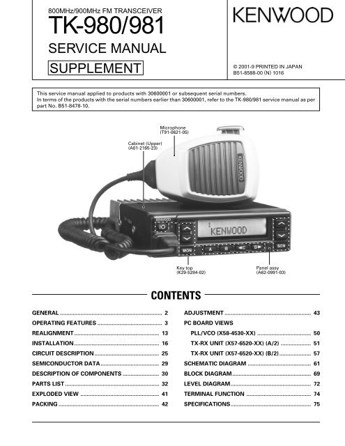
800MHz/900MHz FM TRANSCEIVER<strong>TK</strong>-980/<strong>981</strong>SERVICE MANUALSUPPLEMENT© 2001-9 PRINTED IN JAPANB51-8588-00 (N) 1016This service manual applied to products with 30600001 or subsequent serial numbers.In terms of the products with the serial numbers earlier than 30600001, refer to the <strong>TK</strong>-980/<strong>981</strong> service manual as perpart No. B51-8478-10.Cabinet (Upper)(A01-2165-23)Microphone(T91-0621-05)Key top(K29-5284-02)Panel assy(A62-0991-03)CONTENTSGENERAL ................................................................. 2OPERATING FEATURES ......................................... 3REALIGNMENT...................................................... 13INSTALLATION...................................................... 16CIRCUIT DESCRIPTION......................................... 25SEMICONDUCTOR DATA..................................... 29DESCRIPTION OF COMPONENTS ....................... 30PARTS LIST ............................................................ 32EXPLODED VIEW .................................................. 41PACKING ................................................................ 42ADJUSTMENT ....................................................... 43PC BOARD VIEWSPLL/VCO (X58-4530-XX) .................................. 50TX-RX UNIT (X57-6520-XX) (A/2) ................... 51TX-RX UNIT (X57-6520-XX) (B/2).................... 57SCHEMATIC DIAGRAM ........................................ 61BLOCK DIAGRAM.................................................. 69LEVEL DIAGRAM................................................... 72TERMINAL FUNCTION ......................................... 74SPECIFICATIONS................................................... 75
<strong>TK</strong>-980/<strong>981</strong>GENERALINTRODUCTIONSCOPE OF THIS MANUALThis manual is intended for use by experienced techniciansfamiliar with similar types of commercial grade communicationsequipment. It contains all required service informationfor the equipment and is current as of the publicationdate. Changes which may occur after publication arecovered by either <strong>Service</strong> Bulletins or <strong>Manual</strong> Revisions,which are issued as required.ORDERING REPLACEMENT PARTSWhen ordering replacement parts or equipment information,the full part identification number should be included.This applies to all parts : components, kits, and chassis. Ifthe part number is not known, include the chassis or kitnumber of which it is a part, and a sufficient description ofthe required component for proper identification.PERSONNEL SAFETYThe following precautions are recommended for personnelsafety :• DO NOT transmit if someone is within two feet (0.6meter) of the antenna.• DO NOT transmit until all RF connectors are secure andany open connectors are properly terminated.• SHUT OFF and DO NOT operate this equipment nearelectrical blasting caps or in an explosive atmosphere.• All equipment should be properly grounded beforepower-up for safe operation.• This equipment should be serviced by only qualifiedtechnicians.PRE-INSTALLATION CONSIDERNATIONS1. UNPACKINGUnpack the radio from its shipping container and checkfor accessory items. If any item is missing, please contactKENWOOD immediately.2. LICENSING REQUIREMENTSFederal regulations require a station license for each radioinstallation (mobile or base) be obtained by the equipmentowner. The licensee is responsible for ensuring transmitterpower, frequency, and deviation are within the limitspermitted by the station license.Transmitter adjustments may be performed only by a licensedtechnician holding an FCC first, second or generalclass commercial radiotelephone operator’s license. Thereis no license required to install or operate the radio.3. PRE-INSTALLATION CHECKOUT3-1. IntroductionEach radio is adjusted and tested before shipment. However,it is recommended that receiver and transmitter operationbe checked for proper operation before installation.3-2. TestingThe radio should be tested complete with all cabling andaccessories as they will be connected in the final installation.Transmitter frequency, deviation, and power outputshould be checked, as should receiver sensitivity, squelchoperation, and audio output. QT equipment operationshould be verified.4. PLANNING THE INSTALLATION4-1. GeneralInspect the vehicle and determine how and where theradio antenna and accessories will be mounted.Plan cable runs for protection against pinching or crushingwiring, and radio installation to prevent overheating.4-2. AntennaThe favored location for an antenna is in the center of alarge, flat conductive area, usually at the roof center. Thetrunk lid is preferred, bond the trunk lid and vehicle chassisusing ground straps to ensure the lid is at chassis ground.4-3. RadioThe universal mount bracket allows the radio to bemounted in a variety of ways. Be sure the mounting surfaceis adequate to support the radio’s weight. Allow sufficientspace around the radio for air cooling. Position the radioclose enough to the vehicle operator to permit easy accessto the controls when driving.4-4. DC Power and wiring1. This radio may be installed in negative ground electricalsystems only. Reverse polarity will cause the cable fuseto blow. Check the vehicle ground polarity before installationto prevent wasted time and effort.2. Connect the positive power lead directly to the vehiclebattery positive terminal. Connecting the Positive lead toany other positive voltage source in the vehicle is not recommended.CAUTIONIf DC power is to be controlled by the vehicle ignitionswitch, a switching relay should be used to switch the positivepower lead. The vehicle ignition switch then controlsDC to the relay coil.3. Connect the ground lead directly to the battery negativeterminal.4. The cable provided with the radio is sufficient to handlethe maximum radio current demand. If the cable must beextended, be sure the additional wire is sufficient for thecurrent to be carried and length of the added lead.2
GENERAL / OPERATING FEATURES<strong>TK</strong>-980/<strong>981</strong>5. INSTALLATION PLANNING – CONTROL STATIONS5-1. Antenna systemControl station. The antenna system selection dependson many factors and is beyond the scope of this manual.Your KENWOOD dealer can help you select an antenna systemthat will best serve your particular needs.5-2. Radio locationSelect a convenient location for your control station radiowhich is as close as practical to the antenna cable entrypoint. Secondly, use your system’s power supply (whichsupplies the voltage and current required for your system).Make sure sufficient air can flow around the radio and powersupply to allow adequate cooling.SERVICEThis radio is designed for easy servicing. Refer to theschematic diagrams, printed circuit board views, and alignmentprocedures contained in this manual.NoteWhen you modify your radio as described in system setup,take the following precaution.The rating of pin 7 (SB) of the accessory connector cable(KCT-19) on the rear of the radio is 13.6V (1A). Insert a 1Afuse if you use the SB pin for external equipment.131576Accessory connectorcable (KCT-19)13If you do not intend to use the 3.5-mm jack for the externalspeaker, fit the supplied speaker-jack cap (B09-0235-05)to stop dust and sand getting in.Speaker-jack cap(B09-0235-05)+–1. Operation FeaturesThe <strong>TK</strong>-980/<strong>981</strong> is an 800MHz/900MHz band EFJ LTR -compatible trunked radio designed to operate in bothtrunking and conventional modes. The programmable featuresare summarized.This model can handle up to 32 systems with up to 250groups in each system. The transceiver can be used in bothtrunked mode and conventional mode. Systems, groups,and their functions are programmed.2. Transceiver Controls and Indicators (Fig. 1)2-1. Front Panel ControlsAll the keys on the front panel are momentary-type pushbuttons. The functions of these keys are explained below.• POWER keyTransceiver POWER key. When the power is switchedoff, all the parameters, such as the system and group arestored in memory. When the power is switched on again,the transceiver returns to the previous conditions.• SYSTEM UP/DOWN key (Programmable)• SCAN key (Programmable)• MONITOR key (Programmable)• A, B, C and D key (Programmable)• VOLUME UP/DOWN key (Programmable)• BUSY/TX LEDThe BUSY indicator (Green LED) shows that the group isin use. The TX indicator (Red LED) shows that you are transmitting.2-2. Programmable KeysThe FPU (KPG-49D) enables programmable keys to selectthe following functions.Auto tel, AUX-A, AUX-B (Only when voice scrambler isnot selected), DTMF ID (BOT), DTMF ID (EOT), Display character,Emergency (Only foot key), Function, Group down,Group up, Home group, Horn alert, Key lock, Memory (RCL/STO), Memory (RCL), Memory (STO), Message mode (OnlyA key), Monitor A, Monitor B, Monitor C, Monitor D, Publicaddress, Redial, Scan, Scan del/add, Scan temporary delete,Scrambler (Only when voice scrambler is selected), SendGPS, System down, System up, TEL disconnect, Volumedown, Volume up and None.These functions the FPU programs to the function keysand described in the following sections.• Auto TELAutomatically connects available repeaters that are connectedto telephone circuits when operating as LTR system.The time allocated to search for available repeaters is 60seconds, after which connection failure occurs, a DTMFtone is output and the function terminates.If connection to an available circuit is made, only ID 253,EOT or hang-up time-out can terminate the function.3
<strong>TK</strong>-980/<strong>981</strong>OPERATING FEATURES• AUX-AIf this key is pressed, “AUX” icon lights on the LCD andAUX port which is inside of the transceiver turns to the highlevel. If pressed again, the “AUX” icon goes off and theAUX ports turns to the lower level.• AUX-BThis function can be programmed when the voice scramblerboard is not installed.If this key is pressed, an underscore (“_”) appears at theextreme right of the LCD and AUX port which is inside of thetransceiver turns to the active level. If pressed again, theunderscore disappears and the AUX ports turns to thedeactive level.• DTMF ID (BOT)In conventional mode, if you press this key, a predeterminedDTMF ID (Begin of TX) will be sent automatically.• DTMF ID (EOT)In conventional mode, if you press this key, a predeterminedDTMF ID (End of TX) will be automatically sent.• Display characterThis key switches the LCD display between the systemand group number and the system and group name.• EmergencyPressing this key for longer than the programmed “EmergencyKey Delay Time” causes the transceiver to enter theemergency mode. The transceiver jumps to the programmed“Emergency system and group” and transmits forthe programmed “Active Time”.The transceiver disables mic mute while transmitting.After finishing transmission, the transceiver receivers forthe programmed “Interval Time”. The transceiver mutesthe speaker while receiving. Following the above sequence,the transceiver continues to transmit and receive.• FunctionPressing this key causes the transceiver to display“FCN”. Then, pressing a microphone DTMF key causes thecorresponding programmed function to start. This key maybe convenient when using many functions with the microphone12-key keypad.• Group Up/DownWhen the key is pressed each time, the group number tobe selected is incremented/decremented and repeats if heldfor one second or longer.• Home GroupEach pressing of the key selects a preset system/group.• Horn AlertIf you are called from the base station using DTMF whileyou are away from your transceiver, you will be alerted bythe vehicle horn or some other type of external alert. To turnthe horn alert function on , press this key. A confirmationtone sounds, and the display shows “HA” on the sub LCD.If this key is pressed again, the horn alert function isturned off.• Key LockPressing this key causes the transceiver to accept entryof only the [Function], [Key lock], [PTT], [Monitor A], [MonitorB], [Monitor C], [Monitor D], and [Emergency] keys.• Message ModePress this key to enter the message mode. (See “AlphanumericTwo-way Paging Function” for details)• MemoryThis key allows DTMF memory data to be recalled; up to32 memories each with a memory dial of up to 16 digits andan A/N of up to 10 digits per memory.• MonitorUsed to release signalling or squelch when operating as aconventional. It is also used to reset option signalling.• Public AddressPublic address amplifies the microphone audio, and outputsit through a PA speaker. PA is activated by pressingthis key. A confirmation tone sounds, and the displayshows “PUBLIC ADRS”. PA can be activated at anytime(scanning or non-scanning).The RADIO continues to scan & receive calls while in PAmode. Pressing PTT activates PA, and will override an incomingcall at anytime; however, no RADIO transmissiontakes place.If this key is pressed again, a confirmation tone willsound, the display will return to the normal group or SCANdisplay, and the PA function will turn off.• RedialIf you press this key when the system/group is displayed,the last transmitted DTMF code will appear on the display.Pressing the PTT switch at this time will transmit the displayedDTMF code.• ScanPress this key starts scanning. Pressing this key stopsscanning.• Scan Del/AddUsed to select whether system scan routines are usedduring system scan. Each pressing of the key (to ON)toggles between lockout and lock. The scan routine isstarted when on lock. The DEL indicator flashes when thesystem is on lockout.4
OPERATING FEATURES<strong>TK</strong>-980/<strong>981</strong>• Scan Temporary DeleteThis key is temporarily deleted a system being scanned.If you press this key when scan is stopped (when a call isbeing received from another station), the system is temporarilydeleted and scanning restarts.This key operates even when “Scan Type” is set to “ListType System Scan”.• ScramblerIf a scrambler code (1 to 16) has been set in the FPU, anunderscore (“_”) appears at the extreme right of the LCDdisplay when scrambler is active. Pressing this key changeson/off of scramble operation. Press this key for 2 secondsto enter scrambler code selection mode.• Send GPS (Optional)Pressing this key causes the transceiver to send a singleGPS data. (GPS receiver must be installed.)• System Up/DownWhen the key is pressed each time, the system numberto be selected is incremented/decremented and repeats ifheld for one second or longer.• Telephone DisconnectPressing this key ends an RIC connection (disconnectsthe telephone line).• Volume Up/DownWhen the key is pressed, the volume level is increased/decreased and repeats if held for 200ms or longer.• NoneSounds error operation beep, and no action will occur.Use this function when the transceiver is required to bemore simple operated.2-3. Front Panel Displays and Indicators1 Sub displayDisplays the system and group numbers. Also displaysvarious functions, such as TA.2 P (Priority) indicatorThe P indicator ( ) appears when a selected group is programmedas priority, in conventional operation.3 MON (Monitor) indicatorThe MON indicator appears when the button programmedas MONITOR is pressed.45SVC (<strong>Service</strong>) indictorThis icon is not used this transceiver.SCN (Scan) indicatorThe SCN indicator appears when using scan mode.6 AUX (Auxiliary) indicatorappears when the auxiliary function is activated (ON) bypressing the AUX-A key.7 Handset indicatorThe handset indicator ( ) appears when the selectedgroup is programmed as telephone IDs.8 MAIL indicatorFlashes when a status message (FleetSync) is received.Lights when a status message is stored in the stackmemory.9 Alphanumeric displayThe twelve-character dot matrix alphanumeric displayshows the system/group numbers. You can program system/groupnames with up to ten characters in place of thesenumbers. The left display is used as a delete indicator ( )and the right is used for the selective call ( ) or scrambler(_) function. The delete indicator shows*the systemslocked out of the scanning sequence. Selective call andscrambler are optional functions that can be programmed.Displays received messages when using FleetSync.10 A,B,C,D keyThese keys are programmable function (PF) keys.BUSY/ VOLUMETX LED UPVOLUMEPOWER DOWN1 2 34 5 6 7 8SYSTEM UPSYSTEM DOWNMODULARMIC JACKMONITOR10 9SCANFig. 15
<strong>TK</strong>-980/<strong>981</strong>OPERATING FEATURES3. Scan Operating■ System ScanSystem scan can be selected with the “Scan” key by programmingthe scan feature. When the “Scan” key ispressed and the “SCN” mark appears, scan mode in entered.Scanning starts from the system following the currentlydisplayed system. When a call is received, scanningstops, and the system and group are displayed.When programming key is touched during scanning, thescan stops and the revert system or group can be changed.Scanning resumes one second after the key is released.There are two types of system scan.• Fix System ScanAll the set systems except locked-out ones are scanned.If the Del/Add feature is assigned to the programmable key,it can be controlled from the front panel.• List Type System ScanA scan list can be set for each system.The list to be scanned can be changed by changing thedisplay system.If many systems have been set, the scan speed can beincreased by narrowing the systems to be scanned withscan lists.■ System LockoutThe system lockout feature is used to lock systems outof the scan sequence, and can be selected by programmingin the following two ways;• Fixed LockoutThe system to be locked out is selected by programming.When a locked system is selected, the Delete ( ) indicatorappears on the left of the SYSTEM indicator. The revert systemis scanned even if it is locked out. If there is a lockedsystem, the Delete ( ) indicator flashes during fixed scanning.• User Selectable LockoutIf the scan lockout feature is programmed to a key, theuser can lock systems out of the scan sequence with thekey. To lock a system out of the scan sequence, press thekey when the system is displayed. The Delete ( ) indicatoris displayed on the left of the SYSTEM indicator.To unlock a system, select the system and press the key.The Delete ( ) indicator disappears to indicate that the systemhas returned to the scan sequence. The revert systemis scanned even if it is locked out. If there a locked system,the Delete ( ) indicator flashes during fixed scanning. If allsystems are locked out, the scan stops and only the revertsystem is received.■ Drop-out Delay Time (Scan Resume Time)If a call is received during scan, the scan stops. The scanresume time can be programmed as 0 to 300 seconds inone-second increments. The default value is 3 seconds.■ Dwell TimeThe dwell time is the time after transmission ends untilthe scan resumes in scan mode. It can be set 0 to 300 secondsby programming. The default value is 3 seconds.■ System/Group RevertSystem/group revert can be programmed for one of thefollowing;• Last Called RevertThe system or group changes to the revert system orgroup when a call is received with the system or group beingscanned.• Last Used RevertIf a system/group call is received during scanning and thePTT button is pressed for transmission and response withinthe drop out delay time, the system or group is assigned asthe new revert system or group.• Selected RevertIf the system/group was changed while scanning, thenewly selected system/group.• Selected + Talkback RevertIf the system/group was changed while scanning, thenewly selected system/group. The transceiver “talks back”on the current receive group.■ Scan Massage WaitThe time for staying with the home repeater that receivesa signal during system scan and monitoring datamessages can be programmed. If there is no signal fromthe home repeater, the system is scanned for about 50ms.If there is a signal, three data messages are monitored.Normally, three data messages are monitored for each system,and it can be increased in multiples of three data messagesper line to up to eight lines.If the repeater data message indicates that there is nocall, data monitoring is terminated and the home repeater ofthe next system is scanned.■ Group Scan OperationGroup scan can be programmed for each group. In additionto the ID codes of the selected group, the ID codes ofthe other groups that are permitted for group scan are decoded.(The two fixed ID and block decode codes are alwaysdecoded.)If, during group scanning, a call is received with one ofthe selectable group ID codes for which group scan is enabled,the group display indicates the group number that thecall came in with. That group then becomes the new selectedgroup. Group scan resumes after the specified dropoutdelay time or dwell time shared by the system scanelapses.6
OPERATING FEATURES<strong>TK</strong>-980/<strong>981</strong>■ In Conventional SystemIf QT or DQT is set for the group, the groups, includingsignalling, are scanned.In case of the priority group is set in conventional system,if a group scan (including group scan during a system scan)temporarily stops (receiving) in a group that does not havepriority, a look back is performed to the priority group. Lookback is performed according to the look back time A and Bsettings. If a call is received on the priority group, receptionimmediately switches to the priority group.4. Details of Features■ Time-out TimerThe time-out timer can be programmed in 15 secondsincrements from 15 seconds to 10 minutes. If the transmitteris keyed continuously for longer than the programmedtime, the transmitter is disabled and a warning tone soundswhile the PTT button is held down. The alert tone stopswhen the PTT button is released.■ Sub LCD DisplayYou can use 3-digit the display to display the systemnumber or group number. It is useful when the main (12-digit) display indicates system, group name or other functions.■ Selective Call Alert LEDYou can select whether or not the LED on the transceiverflashes in an orange color when selective call was occurred.■ PTT IDPTT ID provides a DTMF or MSK (FleetSync : Fleet-ID)ANI to be sent with every time PTT (beginning of transmission,end of transmission, or both).You can program PTT ID for each group. You can programPTT ID as “on” or “off” when “DTMF” is selected forthe PTT ID type. You can program a PTT ID as “own”, “sel”or “off” when “MSK” is selected for the PTT ID type. Thecontents of ID are programmed for each transceiver.The timing that the transceiver sends ID is programmable.BOT : DTMF ID (BOT)/MSK ID is sent on beginning oftransmission.EOT : DTMF ID (EOT)/MSK ID is sent on end of transmission.Both : DTMF ID (BOT)/MSK ID is sent on beginning oftransmission and DTMF ID (EOT)/MSK ID is sent on endof transmission.■ Off Hook DecodeIf the Off hook decode function has been enabled, removingand replacing the microphone on the hook has noeffect for decoding QT/DQT and option signalling.■ Timed Power OffThis function works as “Automatic Power Switch Off”.Timed power off timer starts from the ignition-off. Afterthe timer expires, the radio will automatically turn off. Thetimer will be reset if the ignition is turned on and off.This function requires ignition-sense. Connect the ignition-lineto the 9-pin connector which is located at the rear ofthe radio.After the timer expires, press the power switch to turnon the radio.■ Horn AlertHorn alert can be set to on or off for each group. If hornalert has been set to YES for a group and DEC ID/QT/DQT/MSK matches, the horn alert, HOR. is turned on and off.The group for which the optional signalling is set works byANDing the decode ID/QT/DQT/MSK with the optional signalling.Either continuous or non-continuous operation can be setby the FPU. The horn alert port is enabled or disabled asfollows;Off hook horn alert Hook off Hook onEnable Yes YesDisable No Yes■ Non-continuousThe horn alert port, HOR, is turned on and off as follows;0.5s 0.5s 0.5s 0.5s 0.5sThe timing when the fixed LTR ID matches is as follows;1s 0.5s 1sHOR■ Radio PasswordWhen the password is set in the transceiver, user can notuse the transceiver unless enter the correct password.This code can be up to 6 digits from 0 to 9 and input withthe key, and “SCN” key.7
<strong>TK</strong>-980/<strong>981</strong>OPERATING FEATURES■ ContinuousHorn alert can be reset by setting an expiration time fromthe FPU, pressing the any key, or setting off hook.Operation when KCT-18 R151 R152is connectedKCT-18 cannot be connected Enable EnablePower on/off and Disable EnableHorn alert on/offHorn alert on/off Enable DisablePower cannot be turned on Disable DisableTX-RX unit A/2Foil side■ Free System RingbackThis feature is available only when a telephone interconnectedID code is selected. If a busy tone sounds when thePTT button is pressed, the transceiver enters this mode automatically.When the PTT button is released, a beep sounds for400ms to indicate that the mode has been entered. If thescan is on, it is resumed (the “SCN” mark goes on). Whenany repeater becomes available, a ringing tone sounds andthis mode ends.The mode is terminated when the system, group, scan,PTT, key is changed.■ System SearchThis feature can be programmed to automatically accessother programmed systems when the selected system cannotbe accessed. If an intercept tone sounds when the PTTbutton is pressed after setting the mode, the transceiverhas entered the mode.If the group ID is a telephone interconnect ID, the transceiverthen attempts to access, in succession, other systemsthat have a telephone interconnect ID in the revertgroup location. If the group ID is a dispatch ID, the transceiverattempts to access other systems that have a dispatchID programmed in the revert group location.If there is no system to be accessed, an intercept tonesounds, the mode is terminated, and the transceiver returnsto the first system. If the access is successful, the mode isterminated, and the searched system becomes the new selectedsystem (If during scanning, the scan stops).R152R151Q27■ TranspondThis feature can be programmed to turn on and off foreach group. If the ID of the group for which transpond isenabled is received, two data messages (transmit ID andturn-off code) are automatically transmitted if the PTT buttonis not pressed as a response within the time set (0 to300 seconds in 1-second increments). If the PTT button ispressed within the time, the transpond is not preformed.■ Data TX with QT/DQTWhether programmed QT/DQT is modulated or not witha data transmission except for Selcall. A radio unit can receivea data message regardless of QT/DQT if the receivingunit is not scanning.■ Call IndicatorThe call indicator can be programmed for each group. Intrunked system, it can be set to respond to a selectable decodeID or one of two fixed IDs, except block IDs. When acall is received with a selectable decode ID, the call indicatorflashes. When a call is received with a fixed ID, the callindicator lights continuously.On a conventional system, the call indicator can be programmedto light for each QT or DQT code. It keeps flashingwhile a call is being received. It is turned off by pressingany front panel key.■ Transmit InhibitThe transceiver can be programmed with a transmit inhibitblock of ID codes. If an ID code within this block isdecoded the preset time before the PTT button is pressed,transmission is inhibited. The BUSY indicator lights and abusy tone sounds until the PTT button is released to indicatethat transmission is not possible (except clear-to talk mode).Transmission with the group for which the encode ID isnot set is inhibited, and the busy tone is output while thePTT button is held down, regardless of the clear-to talk setting.8
OPERATING FEATURES<strong>TK</strong>-980/<strong>981</strong>■ Auto TELA telephone interconnect call can be made by simplypressing the key by assigning this feature to the key. Thisfeature accesses the TEL channel of the available systemautomatically.When the key is pressed, a queue tone is output, and the“AUTO TEL” appears on the alphanumeric display alongwith a flashing handset indicator ( ) to indicate that thismode has been entered. If the TEL ID is set for the revertsystem, the TEL channel of that system is accessed. If allTEL channels are busy, an attempt is made to access theTEL channels of another system in which the TEL ID codehas been programmed. It is repeated for 60 seconds untilthe access succeeds. If the access succeeds, a dial tonereturns from the repeater. If the key is pressed again whenthe queue tone is sounding, this mode is canceled.If the access fails after 60 seconds, a deny tone is outputand this mode is terminated. When the talk ends, the revertsystem/group returns. When the scan mode is effective,the scan resumes. The Auto TEL feature can be programmedto turn on or off for each system.■ ARQ ModeIf affects Trunking mode only. Automatic RepeatreQuest (ARQ) mode is a manner to minimize the air trafficof data communication. Also, it enables to occupy thetrunking repeater channel for the data communication period.5. Option Signalling5-1. DTMFBuilt-in DTMF decoder is available for option signalling.It is possible to use individual call, group call, D.B.D.(Dead Beat Disable). D.B.D. is used with DTMF only.If the option signalling matches, a predetermined actionwill occur.If option signalling matches on a group which is set upwith option signalling, the option signalling indicator (* ) willflash and option signalling will be released. The transpondor alert tone will sound.If the selective call alert LED is set up, the orange LEDwill flash.While option signalling matches (or if option signalling isdeactivated when you are transmitting), you can mute orunmute ID/QT/DQT/Carrier.■ AND/ORYou can select AND or OR for option signalling matchconditions.ANDORANDORAlert/TranspondQT/DQT/ID+DTMF; Option matches = ActionQT/DQT/ID+DTMF; Option matches = ActionAF mute openQT/DQT/ID+DTMF; Option matches = ActionQT/DQT/ID; Signalling only matches = ActionWith OR set up, alert/transpond will not function withonly DTMF.With OR set up, AF mute will not release when onlyDTMF matches.With a conventional group not set up with QT or DQT,only the carrier is considered when signalling matches.■ Auto ResetIf option signalling matches a group set up with optionsignalling, option signalling is released. After matching optionsignalling, option signalling will temporarily reset automatically.■ Dead Beat DisableIf the D.B.D. code matches, a predetermined action willoccur. Whether option signalling is activated or not, whenD.B.D. matches on any group, the transceiver will becomeTX inhibited or TX/RX inhibited. While D.B.D. is active, if theD.B.D. code + “#” code is received, D.B.D. will disactivate.When D.B.D. matches, transpond will function. Alert willnot be output, and option signalling match icon will not appear.5-2. MSKBuilt-in MSK (FleetSync : Fleet-ID) decoder is availablefor option signalling. When the group ID matches, squelchremains muted while the station waits for reception ofproper MSK signal. When MSK signal matches, squelchunmutes.■ AND/ORAND : QT/DQT/ID + MSK to unmute. MSK matches =alert toneOR : QT/DQT/ID to unmute. MSK matches = alert tone6. Alphanumeric Two-way Paging Function(FleetSync)■ GeneralThe Alphanumeric Two-way Paging Function(FleetSync) is a Kenwood proprietary protocol. It enablesa variety of paging functions.■ ID ConstructionA radio unit ID is defined by a combination of 3-digit Fleetand 4-digit ID numbers. Each radio unit must be assigned itsown Fleet and ID numbers.■ PTT IDA pre-programmed unique ID (own) can be sent at thebeginning of transmission and/or the end of transmission toidentify which radio unit is on air.When selecting (sel) for MSK ID, the radio calls he specificFleet user the same as selective call.9
<strong>TK</strong>-980/<strong>981</strong>OPERATING FEATURES■ Selective Call (SELCALL)This is a voice call to a particular individual or group ofstations.• Example of Call Types;[100][ALL ] : All the units whose fleet number is “100” are called.[100][1000] : The unit, whose the fleet number is “100” and ID numberis “1000”, is called.[ALL][ALL ] : All the units are called.[ALL][1000] : All ID “1000” are called regardless of their fleet number.• Unit ID Encode BlockEncode ID Block can be set to limit manual dial ID. Theradio unit will not accept an ID other than these IDs whichare entered from the keypad. If Inter-fleet Call is enabled,block ID setting affects each fleet group.■ Status MessageUsing a 2-digit number, you can send and receive a Statusmessage which may be decided in your talk group. EachStatus may be displayed with 16 alphanumeric characters ifprogrammed in the radio. A maximum of 9 received messagescan be stored in the stack memory, and it can be reviewedafter reception. If the message memory becomesfull, the oldest one will be erased. The stack memory will becleared by turning radio power off.• Status 80~99 (Special)Status numbers from 80 to 99 are reserved for specialpurposes. Entering these statuses from the DTMF keypadcan be inhibited.Please notice that the following status numbers are usedfor special purposes;80~87 : Reserved for future use.88 : Terminates to emergency mode.89 : Request for horn alert.90 : Remote stun on. Disable the received radio unit’sTX.91 : Remote stun on. Disable the received radio unit’sTX/RX.92 : Cancel remote stun. Enable the received radio unit’sTX/RX.93 : Acknowledgement status sent when the radio unit isin stun mode (TX disabled).94 : Acknowledgement status sent when the radio unit isin stun mode (TX/RX disabled).95~97 : Reserved for future use.98 : Man down emergency status (For portable).99 : Emergency Status.Note : Remote stun works with DTMF D.B.D. function also.• Automatic Status ResponseIf you pre-select a status number and leave the radio inthe Status Mode, it can automatically respond with the selectedstatus number upon request from the base station.(The request function is initiated by serial control on thebase station (Optional).)■ Short Messase (Optional)A maximum of 48 characters can be sent (External equipmentis required). Received Short Messages will be displayedin the same manner as a Status Message. A maximumof 4 received messages can be stored in the stackmemory. In the Stack Mode, 3-digit LCD indicates the receivedShort Message as “M01”~”M04".■ Long Message (Optional)A maximum of 1024 characters can be sent (Externalequipment is required). Received Long Message will not bedisplayed or stacked in the radio memory but is outputthrough the COM (Data) port.■ Emergency FunctionEmergency status 99 will be sent at the beginning ofeach emergency transmission.• Emergency Status responseEither “Horn” or “Alert” can be selected for the calledradio unit’s response to reception of status 99 which is usedas an emergency status.■ Other Functions• <strong>Manual</strong> DialFleet, ID and Status numbers can be entered from DTMFkeypad. (DTMF microphopne is required.)• FleetSync Baud RateMSK data baud rate setting. The same rate must be setas a communication partner.1200bps :Data communication is made in 1200bps. The communicationarea is much wider than 2400bps. Recommendedfor repeater operation.2400bps :Data communication is made in 2400bps. The communicationarea is narrower than 1200bps, but it will decreasethe data traffic. Data rate 2400bps may not work properlydepending on the repeater’s characteristic.• Message Mode TimerMessage Mode Timer is a delay timer returning frommessage/stack mode to Normal mode.• Status/Short/Long Message on Data GroupStatus/Short/Long Message transmission is madewhether on the Data System/Group.10
OPERATING FEATURES<strong>TK</strong>-980/<strong>981</strong>• Status/Short/Unit ID Message Serial Output(Option)Whether a received Status/Short message or PTT ID isoutput or not from serial port.• Caller ID DisplayPTT ID is displayed on LCD.• Call Alert (Continuous)The radio can provide the alert tone repeatedly until nextoperation.• PTT ID SidetoneThis function allows a single beep sound after the PTT ID(MSK) for FleetSync signalling is encoded.• Caller ID StackThe radio stores the last 3 received caller IDs to volatilememory.■ GPS Report (Optional)ANMEA-0183 GPS unit must be installed.• GPS Report ModeGPS data can be sent automatically or upon request.<strong>Manual</strong>ly sending GPS data works regardless of this setting.Auto : GPS data is sent both automatically and by request.GPS Auto TX Interval and GPS Time Mark mustbe adjusted if required.Poll : GPS data is sent upon request from dispatcher.• GPS Report IntervalInterval time between automatic GPS data transmissions.• GPS Time Mark (Per Mobile)The amount of time from the 0 (zero) minute of the standardizedGPS UTC time to starting the first transmission ofGPS data. It must be set to a different value for each radiounit to avoid a transmission crash.• Send GPSPressing this key causes the transceiver to send a singleGPS data.• GPS Report On Data GroupGPS data transmission is made on the Data System/Group.• Received GPS Data OutputAny selected sentence can be output through the radioserial port (COM0 or COM1).1) MAP HEADER NMEA1 ($GPGGA), NMEA2 ($GPGLL),NMEA3 ($GPRMC)NMEA-0183 standard command. This should be set accordingto your PC application.2) MAP HEADER KW1 ($PKLDS)This is a Kenwood original sentence which consists of“$GPGLL + Fleet + ID + Status”. This item should be setaccording to your PC application.3) MAP HEADER KW2 ($PKLID)This is a Kenwood original sentence which consists of“Fleet + ID”. This should be set according to your PCapplication.■ Parameters• GTC CountNumber of Go To data Channel messages to be sent beforetransmitting a data message if it is being made on DataSystem/ Group. If a radio unit receives a GTC message, itwill move to the Data System/Group of the current system.Increase this item to make sure the called radio unit movesto the Data System/Group.• Random Access (Contention)When a channel (or all the repeater channels for Trunkingmode) is busy, radio unit will not transmit (depending on itsBusy Channel Lockout setting in conventional mode). Assoon as a channel is cleared, some transmissions maycrash. Random access is used to avoid this by employing arandom transmission sequence.• Number of RetriesNumber of Retries is the maximum number of retrytransmission when no acknowledgement is received in theMaximum ACK Wait Time. Increase this item to improvedata communication reliability.• TX Busy Wait TimeTX Busy Wait Time is the maximum amount of time beforegiving up the data transmission when the channel (or allthe repeater channels for Trunking mode) is busy. Also, thistimer affects if it expires during Random Access period.• Maximum ACK Wait TimeMaximum ACK Wait Time is the maximum amount oftime to wait for an acknowledgement from the called radiounit. It is used as an interval time of retries. It must be setgreater than the ACK Delay Time of the called radio unit.11
<strong>TK</strong>-980/<strong>981</strong>OPERATING FEATURES• ACK Delay TimeACK Delay Time is the amount of time from the end ofreceiving a data to the beginning of sending anacknowledgement. It should be adjusted as the repeater’shang-up delay time. Also, it must be set less than the MaximumACK Wait Time of the calling radio unit.• TX Delay Time (RX Capture)TX Delay Time is the amount of unmodulated transmissionto let the called unit stop scanning or exit its batterysave mode. It is used only when starting a data communicationsequence.• Data TX Modulation Delay TimeData TX Modulation Delay Time is the amount of timefrom the beginning of transmission to the beginning of adata modulation. It is used every time data is transmitted.It must be set to more than 300ms if data communication ismade in Trunking Mode.7. Audible User Feedback TonesThe transceiver outputs various combinations of tones tonotify the user of the transceiver operating state. The maintones are listed below.The high tone is 1477Hz, the mid tone is 941Hz, and thelow tone is 770Hz.■ Power On ToneThis tone is output when the transceiver is turned on.(The high tone is output for 500ms.)■ Alert ToneThis tone is output when the transceiver is TX inhibitionfor TOT and PLL unlocked. It is output until the PTT buttonis released. (The 697Hz tone is output.)■ DBD On ToneWhen a D.B.D. code is received, transpond tone sounds.■ DBD Off ToneWhen a D.B.D. release code is received, transpond tonesounds.■ Password Agreement ToneWhen the correct password is entered, the tone sounds.The optional feature’s control tone can be set to yes or no.■ PTT Release ToneWhen you release the PTT switch, the PTT release tonesounds.■ Busy ToneSounds in LTR mode, when you cannot use a repeater(system busy or TX inhibit). Sounds in conventional mode,when busy channel lockout is functioning. You can selectyes or no for the optional feature’s warning tone.■ Group Call ToneSounds when a group call with the correct DTMF optionsignalling is received, repeats 7 times. You can select yes orno for the optional feature’s warning tone.■ Individual Call ToneSounds when an individual call with the correct DTMFoption signalling is received. You can select yes or no forthe optional feature’s warning tone.■ Key Press Tone [A]Sounds when a key is pressed. For toggle keys, soundswhen toggle function is turned on (key press tone [B]sounds when it is turned off). You can select yes or no forthe optional feature’s control tone.■ Key Press Tone [B]Sounds when a key is pressed. For toggle keys, soundswhen the toggle function is turned off (key press tone [A]sounds when it is turned on). You can select yes or no forthe optional feature’s control tone.■ Key Press Tone [C]Sounds when a key is pressed. Also sounds when storingdata, adding a DTMF code to memory, and when changingtest mode settings. You can select yes or no for theoptional feature’s control tone.■ Key Input Error ToneSounds when a key is pressed but that key cannot beused. You can select yes or no for the optional feature’swarning tone.■ Roll Over ToneSounds at the smallest system/group. You can selectyes or no for the optional feature’s control tone.■ Transpond ToneSounds when an individual call with the correct LTR/DTMF option signalling is received. For group calls, only thegroup tone will sound, not the transpond tone.■ Intercept ToneThis tone indicates that the transceiver is out of range. Itindicates that the PTT button is pressed, and transmissionhas started, but the repeater cannot be connected and talkingis not possible. It is output until the PTT button is released.(The mid tone and low tone are output alternately in200ms intervals.)■ Delay ToneThis tone is output when the PTT button is pressed andthe repeater is accessed three times or more to indicateconnection with the repeater is delayed. This tone is thesame as the busy tone. (It is not output of clear to talk hasbeen set to yes.)12
OPERATING FEATURES / REALIGNMENT<strong>TK</strong>-980/<strong>981</strong>■ Proceed ToneThis tone is output when the PTT button is pressed,transmission starts, and the repeater is connected to indicatethat the user can talk if the clear to talk function hasbeen set. (The high tone is output for 100ms.)REALIGNMENT1. ModesUser mode■ Queue ToneThis tone is output until the auto TEL function is set andthe TEL channel is accepted successfully. (The mid tone onfor 50ms, off for 50ms, and on for 50ms in 1 second intervals.)Panel test modePC modeFirmware programmingmodePanel tuning modeData programmingmodePC test modePC tuning mode■ Deny ToneThis tone is output if the auto TEL function is set, thequeue tone is output, but the TEL channel cannot be accessedwithin 60 seconds. It is similar to the intercept tone.(The mid tone and low tone are output alternately in 150msintervals.)■ Free System Ringback Mode Tone, SystemSearch Mode ToneThis tone indicates that the transceiver is free systemringback mode or system search mode. (The mid tone isoutput for 400ms.)■ Ringing ToneThis tone indicates that the transceiver can use the repeaterin free system ringback mode. (The mid tone and notone are output eight cycles alternately in 50ms intervals.)■ System Search ToneSounds when the system changes during system search.You can select yes or no for the optional feature’s warningtone.Clone modeModeUser modePanel test modePanel tuning modePC modeData programmingmodePC test modeFirmware programmingmodeClone modeFunctionFor normal use.Used by the dealer to check the fundamentcharacteristics.Used by the dealer to tune the radio.Used for communication between theradio and PC (IBM compatible).Used to read and write frequency dataand other features to and from the radio.Used to check the radio using the PC.This feature is included in the FPU.See panel tuning.Used when changing the main programof the flash memory.Used to transfer programming data fromone radio to another.■ System Search End ToneSounds when a possible connection to a repeater in systemsearch is not mode. You can select yes or no for theoptional feature’s warning tone.2. How to Enter Each ModeModeOperationUser modePower ONPanel test mode[A]+Power ON (Two seconds)PC modeReceived commands from PCPanel tuning mode[Panel test mode]+[SCN]Firmware programming mode [SCN]+Power ON (Two seconds)Clone mode[C]+Power ON (Two seconds)3. Panel Test ModeSetting method refer to ADJUSTMENT.4. Panel Tuning ModeSetting method refer to ADJUSTMENT.13
<strong>TK</strong>-980/<strong>981</strong>REALIGNMENT5. PC Mode5-1. PrefaceThe transceiver is programmed by using a personal computer,programming interface (KPG-46) and programmingsoftware (KPG-49D).The programming software can be used with an IBM PCor compatible. Figure 1 shows the setup of an IBM PC forprogramming.5-2. Connection Procedure1. Connect the transceiver to the personal computer withthe interface cable.2. When the Power switch on, user mode can be enteredimmediately. When PC sends command the radio enterPC mode, and “PROGRAM” is displayed on the LCD.When data transmitting from transceiver, the red LED isblinking.When data receiving to transceiver, the green LED isblinking.Notes :• The data stored in the personal computer must matchmodel type, when it is written into the flash memory.• Change the transceiver to PC mode, then attach the interfacecable.5-3. KPG-46 Description(PC programming interface cable : Option)The KPG-46 is required to interface the transceiver to thecomputer. It has a circuit in its D-subconnector (25-pin) casethat converts the RS-232C logic level to the TTL level.The KPG-46 connects the modular microphone jack ofthe Ttransceiver to the computers RS-232C serial port.5-4. Programming Software DescriptionThe KPG-49D programming disk is supplied in 3-1/2" diskformat. The software on this disk allows a user to programthe transceiver radio via programming interface cable (KPG-46).IBM-PCKPG-465-5. Programming With IBM PCIf data is transferred to the transceiver from an IBM PCwith the KPG-49D, the destination data (basic radio information)for each set can be modified. Normally, it is not necessaryto modify the destination data because their values aredetermined automatically when the frequency range (frequencytype) is set.The values should be modified only if necessary.Data can be programmed into the flash memory in RS-232C format via the modular microphone jack.KPG-49D instruction manual parts No. : B62-1096-XX.6. Firmware Programming Mode6-1. PrefaceFlash memory is mounted on the transceiver. This allowsthe transceiver to be upgraded when new features arereleased in the future. (For details on how to obtain thefirmware, contact Customer <strong>Service</strong>.)6-2. Connection ProcedureConnect the transceiver to the personal computer (IBMPC or compatible) with the interface cable (KPG-46). (Connectionis the same as in the PC Mode.)6-3. Programming1. Start up the programming software (KPG-49D), select“firmware program” in the “Program” item, and pressthe Return key on the personal computer. This starts upthe firmware programmer.2. The top screen is displayed. Press any key to advance tothe next screen.3. Set the communications speed (normally, 57600 bps)and communications port in the Setup item.4. Set the firmware to be updated by File select (=F1).5. Turn the transceiver Power ON with the [SCN] switchheld down. Hold the switch down for two seconds untilthe display changes to “PROG 57600”. When “PROG57600” appears, release your finger from the switch.6. Check the connection between the transceiver and thepersonal computer, and make sure that the transceiver isin the Program mode.7. Press F10 on the personal computer. A window openson the display to indicate progress of writing. When thetransceiver starts to receive data, the [P] icon is blinking.8. If writing ends successfully, the LED on the transceiverlights and the checksum is displayed.9. If you want to continue programming other transceivers,repeat steps 5 to 8.14KPG-49DFig. 1<strong>TK</strong>-980/<strong>981</strong>Notes :• To start the Firmware Programmer from KPG-49D, theFpro path must be set up by KPG-49D setup.• This mode cannot be entered if the Firmware programmingmode is set to Disable in the Programming software(KPG-49D).• When programming the firmware, it is recommend tocopy the data from the floppy disk to your hard disk beforeupdate the radio firmware.Directly copying from the floppy disk to the radio may notwork because the access speed is too slow.
REALIGNMENT<strong>TK</strong>-980/<strong>981</strong>6-4. Function1. If you press the [MON] switch while “PROG 57600” isdisplayed, the checksum is displayed. If you press the[MON] switch again while the checksum is displayed,“PROG 57600” is redisplayed.2. If you press the [D] switch while “PROG 57600” is displayed,the display changes to “PROG 19200” to indicatethat the write speed is low speed (19200 bps). If youpress the [D] switch again while “PROG 19200” is displayed,the display changes to “PROG 38400”, and thewrite speed becomes the middle speed (38400 bps). Ifyou press the [D] switch again while “PROG 38400” isdisplayed, the display returns to “PROG 57600”.Note :Normally, write in the high-speed mode.6. Press the [SCN] key on the master while the master displays“CLONE MODE”. The data of the master is sent tothe slave. While the slave is receiving the data, “PRO-GRAM” is displayed. When cloning of data is completed,the mater displays “END”, and the slave automaticallyoperates in the User mode. The slave can then be operatedby the same program as the master.7. The other slave can be continuously cloned. When the[SCN] key on the master is pressed while the master displays“END”, the master displays “CLONE MODE”.Carry out the operation in step 4 to 6.Note :Only the same models can be cloned together.7. Clone ModeProgramming data can be transferred from one radio toanother by connecting them via their modular microphonejacks. The operation is as follows (the transmit radio is themaster and the receive radio is a slave).1. Turn the master radio power ON with the [C] key helddown. If the password is set to the radio, the radio displays“CLONE LOCK”. If the password is not set, theradio displays “CLONE MODE”.2. When “CLONE LOCK” is displayed, only the [System up/down] key and [SCN], and [0] to [9] keys can be accepted.When you enter the correct password, and “CLONEMODE” is displayed, the radio can be used as the cloningmaster. The following describes how to enter the password.3. How to enter the password with the microphone keypad.If you press a key while “CLONE LOCK” is displayed, thenumber that was pressed is displayed on the radio. Eachpress of the key shifts the display in order to the left.When you enter the password and press the [SCN] key,“CLONE MODE” is displayed if the entered password iscorrect. If the password is incorrect, “CLONE LOCK” isredisplayed.How to enter the password with the [System up/down]key;If the [System up/down] key is pressed while “CLONELOCK” is displayed, numbers (0 to 9) are displayed flashing.When you press the [SCN] key, the currently selectednumber is determined, and the display shifts tothe left. If you press the [SCN] key after entering thepassword in this procedure, “CLONE MODE” is displayedif the entered password is correct. If the passwordis incorrect, “CLONE LOCK” is redisplayed.4. Power on the slave radio.5. Connect the cloning cable (No. E30-3382-05) to themodular microphone jacks on the master and slave.Cloning cable(E30-3382-05)Fig. 215
<strong>TK</strong>-980/<strong>981</strong>INSTALLATION1. Accessory Connection Cable(KCT-19 : Option)The KCT-19 is an accessory connection cable for connectingexternal equipment. The connector has 15 pins andthe necessary signal lines are selected for use.1-1. Installing the KCT-19 in the transceiver1. Remove the upper and lower halves of the transceivercase, and lift the DC cord bushing ( 1 ) from the chassis.2. Remove the pad as shown in Figure 1 ( 2 ).3. Insert the KCT-19 cable ( 3 ) into the chassis ( 4 ).The wire harness band ( 5 ) must be inside the chassis.4. Replace the DC cord bushing ( 6 ).5. Connect the KCT-19 to the TX-RX unit (A/2) as shown inFigure 2 ( 7 ).6. Connect the KCT-19 to the external accessory by insertingthe crimp terminal ( 8 ) into the square plug ( 9 ),both of which are supplied with the KCT-19.12Fig. 11-2. Accessory Port FunctionNo. (A) No. (B,C,D,E) Name Function Note1 D-2 AHK External hook input *1BUSY System busy output2 D-5 ME Microphone ground *1AM Speaker audio mute input3 D-3 IGN Ignition sense input4 D-1 DEO Receiver detector output5 D-6 MI External microphone input *1TXS Transmitter sense output6 B-2 E Ground7 B-3 SB Switched B+, DC 13.6V output.Maximum 1A8 D-7 PTT External PTT input, active low.During DTC is low, it works asDATA PTT.9 D-4 DI Data modulation input10 B-1 HOR Horn alert/call output11 D-8 SQ Squelch detect output (Conventional)/Logic squelch output (LTR), active low.12 C-1 SP Speaker audio output.13 E-1 CN2 LOK Link complete pulse output. *2andCN4CN2 AM Speaker mute input.14 E-2 CN4 RXD Serial control data input *2CN2 MM MIC mute input, active high.15 E-3 CN4 TXD Serial control data output. *2CN2 DTC Data control channel signal input,Data channel : LowLOK Link complete pulse output.TXS Transmitter sense output,Active highFSW Foot switch input, active lowDEBC7CN4 CN1CN3 CN2CN6ECBD5643A9 Square plug(E09-1571-05)113 3Contact15 12 8Crimp terminal(E23-0613-05)Note*1 : The functions of A-1, A-2 and A-5 are changed as described inthe jumper chart.*2 : The functions of A-13, A-14 and A-15 are changed if the connectorE is connected to CN2 or CN4 of the radio.No. CN2 CN4E-1 LOK/AM LOKE-2 MM RXDE-3 LOK/DTC/TXS/FSW TXD· Connect CN6 of the radio to connector C of the KCT-19 instead ofto the internal speaker connector, if use external speaker.Fig. 216
INSTALLATION<strong>TK</strong>-980/<strong>981</strong>1-3. Data Equipment ConnectionThe jumpers must be set to either one for each function.Otherwise, the radio will not work properly.AHK/BUSYR64 (0Ω) R18 (0Ω)FunctionYes No BUSY System busy output indicates if norepeater channel is available in thecurrently selected LTR systemwhen PTT is pressed, active low: DefaultNo Yes AHK MIC hook input/RXD2 (com2).ME/AMR12 (0Ω) R167 (0Ω)FunctionYes No AM Speaker mute input, active high: DefaultNo Yes ME MIC ground.MI/TXSR94 (0Ω) R24 (0Ω)FunctionYes No TXS Transmitter sense output, activehigh : DefaultNo Yes MI Internal MIC input.LOK/AMR5 (0Ω) R6 (0Ω) FunctionYes No AM Audio mute signal input.No Yes LOK Link complete pulse output : DefaultDTC/LOK/TXS/FSWR168 R84 R51 R13 Function(0Ω) (0Ω) (0Ω) (0Ω)No No No Yes LOK Link complete pulse output.Yes No No No DTC Data control channel signal input,Data channel : low (Default)No No Yes No TXS Transmitter sense output,active highNo Yes No No FSW Foot switch input, active lowR51R13R167R12R24R94TX-RX unit (A/2)Foil side viewR168R18R64R84Note : The following parts are not installed at the time ofshipping; R5,R13,R18,R24,R51,R84,R1672. Accessory Terminal (TX-RX Unit)2-1. External Connector Accessory Terminal MethodConnector Pin Pin I/O FunctionNo. No. nameCN1 1 DEO O Detect signal output. (Output level :(DO) 250mVrms; standard modulation)2 AHK I external hook signal input.(AH) “COM2” port must be select “AUXHOOK/PTT” / “DATA PTT” functionin the KPG-49D.On hook : L, Off hook : HBUSY O System busy signal output fortrunking system. No vacant repeater: L, Vacant repeater : HRXD2 I Serial data input 2.“COM2” port must be select“REM” / “DATA” / “DATA+GPS”function in the KPG-49D.3 IGN (IG) I Ignition input for KCT-18.4 DI I External modulation signal input.5 ME – MIC earth.AM I Audio mute signal input.6 MI I Internal MIC input.TXS O Signal indicating whether thetransceiver is transmitting or not.TX : H, Another : L7 PTT I External PTT signal input.(PT) “COM2” port must be select“AUX HOOK/PTT” / “DATA PTT”function in the KPG-49D.TX : L, Another : HTXD2 O Serial data output 2.“COM2” port must be select“REM” / “DATA” / “DATA+GPS”function in the KPG-49D.R6R5TX-RX unit (A/2)Component side view17
<strong>TK</strong>-980/<strong>981</strong>INSTALLATION18Connector Pin Pin I/O FunctionNo. No. name8 SQ O Squelch signal output. Signal logictype can select “Carrier operaterelay” or “Tone operate relay”.Active logic level or type can selectin the KPG-49D.CN2 1 AM I Audio mute signal input.LOK O Access logic signal output.Active level or type can be selectablein the KPG-49D.2 MM I MIC mute input.3 DTC I Data control channel signal input.Data channel : L, Normal channel : HTXS O Signal indicating whether the transceiveris transmitting or not.TX : H, Another : LFSW I Foot switch signal input.Foot sw on : L, Foot sw off : HLOK O Access logic signal output.Active level or type can be selectablein the KPG-49D.CN3 1 HOR O Horn alert signal output. Signaloutput for horn relay drive (opencollector). L level during horn drive :Max. sink current 100mA.2 E – Earth.3 SB O Power output after power switch(DC 13.6V± 15%, 0.75A max.).CN4 1 LOK O Access logic signal output.Active level or type can be selectablein the KPG-49D.2 RXD1 I Serial data input 1.“COM1” port must be select “REM”/ “DATA” / “GPS” / “DATA+GPS”function in the KPG-49D.3 TXD1 O Serial data output 1.“COM1” port must be select “REM”/ “DATA” / “GPS” / “DATA+GPS”function in the KPG-49D.CN5 1 PA O Relay for PA function in KAP-1control signal. PA on : H, PA off : L2 SPO O Audio signal input from KAP-1.3 SPI I Audio signal output to KAP-1.CN6 1 SP O Output for internal/external speaker.2 E – Earth.3. Optional Board TerminalTerminal is for mounting the option board are provided atthe TX-RX unit (A/2) and TX-RX unit (B/2). The table belowshows the correspondence between the board and terminals.Disconnect R529 and R571 in control unit when thescrambler board is attached.The table below shown the differences between theschematic terminals and the PC board terminals.Schematic diagramPC board viewName I/O Function Name UnitSB – Switched B+, DC 13.6V SB TX-RX (A/2)output. Maximum 0.75A5C – 5C 5C TX-RX (A/2)GND – Earth E TX-RX (A/2)DEO O Detect signal output (Output DEO TX-RX (A/2)level : 250mVrms; standardmodulation)RXAI I RX audio input RXAI TX-RX (B/2)RXAO O RX audio output RXAO TX-RX (B/2)TXAI I TX audio input TXAI TX-RX (B/2)TXAO O TX audio output TXAO TX-RX (B/2)LOK O Access logic signal output. LOK TX-RX (A/2)Active level or type can beselectable in the KPG-49D.OPT O Option board select. Please OP TX-RX (A/2)(EMG) select option board type in theKPG-49D.OP1 O Option code 1 (for voice C1 TX-RX (A/2)scrambler code 1)OP2 O Option code 1 (for voice C2 TX-RX (A/2)scrambler code 2)OP3 O Option code 1 (for voice C3 TX-RX (A/2)scrambler code 3)OP4 O Option code 1 (for voice C4 TX-RX (A/2)scrambler code 4)SQ O Squelch signal output. Signal SQ TX-RX (A/2)logic type can select “Carrieroperate relay” or “Tone operaterelay”. Active logic level or typecan select in the KPG-49D.TXD1 O Serial data output 1 TD1 TX-RX (A/2)RXD1 I Serial data input 1 RD1 TX-RX (A/2)TXD2 O Serial data output 2 TD2 TX-RX (A/2)RXD2 I Serial data input 2 RD2 TX-RX (A/2)RSSI O Receive signal strength indication RSSI TX-RX (A/2)PTT I PTT PTT TX-RX (B/2)MPTT I MIC PTT MPTT TX-RX (B/2)FSW I Foot switch input FW TX-RX (A/2)ST I Side-tone input ST TX-RX (A/2)
INSTALLATION<strong>TK</strong>-980/<strong>981</strong>SBLOKEDEO RD2 5C C4 C3TD2 RD1 SQ OPTD1 FW C2 C1TX-RX unit (A/2)Foil side viewRSSIKCT-19311315613Contact2KCT-18STFig. 3TX-RX unit (A/2)Component side view4-2. Modifying the TransceiverModify the transceiver as follows to turn the power orthe Horn Alert or <strong>Manual</strong> Relay function on and off with theignition key.1. Remove the lower half of the transceiver case.2. Set jumper resistors (0Ω) R151 and R152 of the TX-RXunit (A/2) as shown in Table 1.RXAOR529PTTMPTTRXAIR152TXAOTXAIR571TX-RX unit (B/2)Foil side viewKCT-19CN7R151TX-RX UNIT(A/2)ANTFig. 44. Ignition Sense Cable (KCT-18 : Option)The KCT-18 is an optional cable for enabling the ignitionfunction. The ignition function lets you turn the power to thetransceiver on and off with the car ignition key.If you use the Horn Alert function or the <strong>Manual</strong> Relayfunction, you can turn the function off while driving with theignition key.4-1. Connecting the KCT-18 to the Transceiver1. Install the KCT-19 in the transceiver. (See the KCT-19section.)2. Insert the KCT-18 lead terminal ( 2 ) into pin 3 of thesquare plug ( 1 ) supplied with the KCT-19, then insertthe square plug into the KCT-19 connector ( 3 ).Operation when KCT-18 is connected. R151 R152KCT-18 cannot be connected. Enable EnablePower on/off and Horn Alert or Disable EnableAUX-A on/off.Horn Alert or AUX-A on/off, Enable DisableTimed power off.Power cannot be turned on. Disable DisableTable 1 R151 and R152 setup chart19
<strong>TK</strong>-980/<strong>981</strong>INSTALLATION5. Connection Cable (KCT-29 : Option)The KCT-29 connection cable kit is used to connect the<strong>TK</strong>-980/<strong>981</strong> transceiver to the KPG-1A Modem GPS Receiveror the KPG-1B Modem GPS Controller.5-1. Installing the KCT-29 in the transceiver1. Remove the upper cover from the transceiver.2. Lift the DC cord bushing ( 1 ) from the chassis.3. Remove the pad as shown in Figure 5 ( 2 ).4. Insert the KCT-29 cable ( 3 ) into the chassis ( 4 ). Thewire harness band ( 5 ) must be inside the chassis.5. Replace the DC cord bushing ( 6 ).6. Connect the KCT-29 to the TX-RX unit (A/2) as shown inFigure 6 ( 7 ).126. Interface Cable (KCT-31 : Option)The KCT-31 is a RS-232C interface cable for LMR mobileradios, <strong>TK</strong>-980/<strong>981</strong>.The 9-pin (D-sub) connector is connected to an externalRS-232C terminal. The other end of the cable is connectedto the internal connector of LMR mobile radio.Note : You cannot write a firmware with the KCT-31.6-1. Features• This KCT-31 has a RS-232C-TTL level interface circuit.• This KCT-31 does not require an external power supply.• This KCT-31 can be used up to 9600 bps.• Compatible with an ER terminal of DTE that has the voltage6V or more.6-2. Terminal function (D-sub connector)Pin No. I/O Port name Function1 I CD Carrier detect2 I RD Receive data3 O SD Transmit data4 O ER Data terminal ready5 – SG Signal ground6 I DR Data set ready7 O RS Request to send8 I CS Clear to send9 – CI Ring indicatorFig. 55196CDBCN4 CN1CN3 CN2BBD5C463AKCT-297Fig. 620
INSTALLATION<strong>TK</strong>-980/<strong>981</strong>6-3. Installing the KCT-31 in the transceiverNote :When the COM1 is used, A connector is unused.When the COM2 is used, C connector is unused.2. Make sure the unit’s power is turned off.3. Remove the upper case of the transceiver and lift the DCcable bushing ( 1 ) from the chassis.4. Remove the pad as shown in Figure 8 ( 2 ).1. Bind the unused connecor to the cable with a retainingband as shown.When the COM1 is used.When the COM2 is used.CAYellowYellowBGreenBGreen1RedRed2BlackBlackACFig. 8A B CCOM1 No Yes YesCOM2 Yes Yes NoFig. 75. Insert the KCT-31 cable ( 3 ) into the chassis ( 4 ).The write retaining band ( 5 ) must be inside the chassis.6. Replace the DC cable bushing ( 6 ).7. Connect the KCT-31 to the TX-RX unit (A/2) as shown inFigure 9 ( 7 ).8. Replace the upper case.AACCN4CN1CN4CN1BBCN3 CN2BCN3 CN254CN6CN6637When the COM1 is used.When the COM2 is used.Fig. 9Note :· The modification must be applied to the <strong>TK</strong>-980/<strong>981</strong>transceivers with a serial number of 30600000 or smallerwhen using a COM2 port. Replace the 47kΩ (R675) chipresistor on the TX-RX unit (B/2) with a 4.7kΩ resistor.· Enable the serial port function on the terminal.· Refer to the service manual of each radio or the help filethat came with the FPU (Field Programming Unit) for details.OriginalNew47kΩ (RK73GB1J473J) → 4.7kΩ (RK73GB1J472J)21
<strong>TK</strong>-980/<strong>981</strong>INSTALLATION7. PA/HA Unit (KAP-1 : Option)7-1. Installing the KAP-1 in the TransceiverThe Horn Alert (max. 2A drive) and Public Address functionsare enabled by inserting the KAP-1 W1 (3P; white/black/red) into CN3 on the TX-RX unit (A/2), inserting W2(3P; green) into CN5 on the TX-RX unit (A/2), and connectingthe KCT-19 (option) to CN2 and CN3 of the KAP-1.HR1 (Default)HR2R1YesNoOutput formHR1HR1• Installation procedure1. Open the upper case of the transceiver.2. Insert the two cables ( 1 ) with connectors from theKAP-1 switch unit into the connectors on the transceiver.3. Secure the switch unit board to the chassis with ascrews ( 3 ). The notch ( 2 ) in the board must beplaced at the front left side.4. Attach the cushion on the top of the KAP-1 switch unit.HR2Cushion(G13-1710-04)43W12CN1CN2CN31W21R1Fig. 11KAP-1 foil side viewCN3CN5• Public addressThe signal from pin 13 of IC7 on the TX-RX unit (A/2)drives PA relay in the KAP-1 and switches the audio poweramplifier output between the external PA system (throughKCT-19) and internal and external speakers.To use the PA function, R109 on the TX-RX unit (A/2)must be removed.Fig. 10KCT-19Use the PA functionDo not use the PA functionR109NoYes7-2. Modifying the Transceiver• Horn alertThe signal from pin 4 of IC7 on the TX-RX unit (A/2) turnsQ4 and Q6 on and off and drives KAP-1 HA relay to drive thehorn with a maximum of 2A.The default output is HR1. The relay open output can beobtained between HR1 and HR2 by removing R1 in the KAP-1.KCT-19R109CN7TX-RX UNIT(A/2)ANTPAFig. 1222
INSTALLATION<strong>TK</strong>-980/<strong>981</strong>• OthersIf the PA and HR2 are not necessary and the speaker outputis output to an external unit through the KCT-19, connectthe KCT-19 C connector to CN6 on the TX-RX unit (A/2).TX-RX UNIT (A/2)IC7Shiftregister4Q1Q613IGNQ6Q58CR58Q4D7CN3W1HORESBKAP-1 (SWITCH UNIT : X41-3380-20)Q1 : DTD114EKD1,2 : 1SS193123R1 0C11000PC5 1000PK2± +D1C6C71000P1000P12123CN1HR2NCCN2HR1ESBCBGRNBRNORGYELKCT-19R3 0K1C3 0.0112CN3PAO/LIOECGRNAudiopower ampIC10+12R109CN6CN5W2PA/LISPOSPI123C21000PR4 0Q1± +D2C4 0.01KCT-19 Terminal13 10 115 12636 : Earth10 : HR112 : PA (HR2)SPEInternal/ExternalspeakerFig. 138. Fitting the Control Panel Upside DownThe <strong>TK</strong>-980/<strong>981</strong> control panel can be fitted upside down,so the transceiver can be mounted with its internal speaker(in the upper half of the case) facing down in your car.1. Remove the control panel and the TX-RX unit (B/2) controlsection. (Fig. 14)2. Fold the flat cable ( 1 ) in the opposite direction ( 2 ).3. Rotate the control section ( 3 ) 180 degrees ( 4 ).4. Insert the flat cable into the control section connector,CN502 ( 5 ).5. Mount the control section on the transceiver ( 6 ).2613CN5025Fig. 144Fig. 1523
<strong>TK</strong>-980/<strong>981</strong>INSTALLATION6. Rotate the control panel 180 degrees and mount it on thetransceiver. Refit the two halves of the case to completeinstallation. (Fig. 16)9-2. KES-4 : OptionThe KES-4 is an external speaker used with the accessoryconnection cable.• Connection procedure1. Install the KCT-19 in the transceiver. (See the KCT-19section.)2. Insert the crimp terminal into the square plug suppliedwith the KCT-19.3. Connect CN5 of the transceiver to connector C of theKCT-19 instead of to the internal speaker connector.KES-41Fig. 1613151236Crimp terminal(E23-0613-05)Black leadBlack/White lead9. External Speaker9-1. KES-3 : OptionThe KES-3 is an external speaker for the 3.5-mm-diameterspeaker jack.• Connection procedure1. Connect the KES-3 to the 3.5-mm-diameter speaker jackon the rear of the transceiver.Fig. 18KES-3Fig. 1724
CIRCUIT DESCRIPTION<strong>TK</strong>-980/<strong>981</strong>Frequency ConfigurationThe TX-RX unit (A/2) incorporates a VCO, based on a fractionalN type PLL synthesizer system, that allows a channelstep of 12.5kHz to be selected. The incoming signal fromthe antenna is mixed with a first local oscillation frequencyto produce a first intermediate frequency of 44.85MHz.The signal is then mixed with a second local oscillationfrequency of 44.395MHz to produce a second intermediatefrequency of 455kHz. This is called a double-conversionsystem. The transmit signal frequency is generated by thePLL VCO, and modulated by the signal from the microphone.It is then amplified by TX amplifier and PA amplifier,and sent to the antenna.<strong>TK</strong>-980<strong>TK</strong>-<strong>981</strong>TX 806~825MHz TX 896~902MHz851~870MHz 935~941MHzRX 851~870MHz RX 935~941MHzANTANTSWRFAMP1stMIXMCF44.85MHzCF 455kHzIF SYSTEMAFO■ AF Signal SystemThe detection signal (DEO) from the TX-RX unit (A/2)goes to the audio processor (IC504) of the TX-RX unit (B/2).The signal passes through a filter in the audio processor toadjust the gain, and is output to IC502. IC502 sums the AFsignal and the DTMF signal and returns the resulting signalto the TX-RX unit (A/2). The signal (AFO) sent to the TX-RXunit (A/2) is input to the D/A converter (IC5). The AFO outputlevel is adjusted by the D/A converter. The signal outputfrom the D/A converter is added with the BEEP signal (BPO)and the resulting signal is input to the audio power amplifier(IC10). The AF signal from IC10 switches between the internalspeaker and speaker jack (J1) output.DEOTX-RX UNIT (B/2)IC504 IC504 IC5AFOAUDIOPROCE.Fig. 3SUMAMPDTMFD/ACONV.BPOAF signal systemIC10AF PASPPAAMP<strong>TK</strong>-980806.15~825.15MHz<strong>TK</strong>-<strong>981</strong>890.15~896.15MHzTXAMPFig. 1<strong>TK</strong>-980806~825MHz851~870MHz<strong>TK</strong>-<strong>981</strong>896~902MHz935~941MHz44.395MHzPLL/VCOVCXO16.8MHzFrequency configurationMDMB■ Squelch CircuitThe detection output from the FM IF IC (IC11) is amplifiedby IC2 and the signal (DEO) is sent to the TX-RX unit (B/2). The signal passes through a high-pass filter and a noiseamplifier (Q503) in the TX-RX unit (B/2) to detect noise. Avoltage is applied to the CPU (IC511). The CPU controlssquelch according to the voltage (ASQ) level. The signalfrom the RSSI pin of IC11 is monitored. The electric fieldstrength of the receive signal can be known before the ASQvoltage is input to the CPU, and the scan stop speed is improved.TX-RX UNIT (B/2)Receiver System■ OutlineAn incoming RF signal from the antenna terminal passesthrough the antenna switch (D208, D209, and D210 are off)and then the bandpass filter (L203). The signal is amplifiedby RF amplifier Q201, and passes through the bandpass filter(L207) again. The resulting signal goes to the first mixer(Q203), where it is mixed with the first local oscillator signaloutput from the frequency synthesizer to produce the firstIF 44.85MHz.IC11IFSYSTEMIC2AMPDEORSSIFig. 4HPFIC503AMPQ503NOISE AMPSquelch circuitD509DETIC511CPUANTD208~210ANTSWL203BPFQ201RF AMPL207BPFQ2031st MIX1st localOSC (PLL)XF1MCFQ151st IFX22ndlocal OSCIC11MIX,DET,IFCF1DET DETIC2AF AMPDEOFig. 2Receiver system25
<strong>TK</strong>-980/<strong>981</strong>CIRCUIT DESCRIPTIONTransmitter System■ OutlineThe transmitter circuit amplifies the desired frequency. ItFM-modulates the carrier signal by means of a varicap diode.■ Younger-stage circuitThe signal output from the VCO is amplified by a bufferamplifier (Q7) and goes to the drive block. The youngerstagecircuit provides a stable drive output without a needfor adjustment. The APC circuit controls voltage in theyounger final stage (Q204).■ VCO/PLL CircuitThe <strong>TK</strong>-980/<strong>981</strong> has a common VCO for the transmitterand the receiver in a sub-unit (A1). It is housed in a solidshielded case and connected to the TX-RX unit (A/2) throughCN101. A filtered low-noise power supply is used for theVCO and varicap diodes.The VCO is described below. It is designed so that Q101turns on with a prescribed frequency when a reverse bias isapplied to D100 and D101 by using the control voltage (CV)through CN101. The control voltage is changed by turningthe trimmer capacitor (TC100). The output from Q103 is appliedto the buffer amplifier (Q102) the output from Q102 isapplied to the doubler (Q100) to generate a VCO output signal.This signal is used as a drive input signal or a local signalof the first mixer. Since a signal output from Q100 is inputto the PLL IC, it passes through CN101 and buffer amplifier(Q300) and goes to the PLL IC (IC300). The modulation signalfrom CN101 is applied to D102 and passes through C106and C107 to modulate the carrier.The PLL IC uses a fractional N type synthesizer to improvethe C/N ratio and lock-up speed. The VCO output signalinput to the pin 5 of the PLL IC is divided to produce acomparison frequency according to a channel step. This signalis compared with the reference frequency which is outputfrom the VCXO (X1). VCXO provides 16.8MHz, 1.5ppm(–30 to +60°C) and guarantees stable performance whenthe temperature changes. The output signal from the phasecomparator passes through a charge pump and an externalactive LPF (Q301, Q302) in the PLL IC to generate a DC VCOcontrol voltage CV. Serial data (DT, CK, EP) are output fromthe CPU (IC511) and shift register (IC8) in the TX-RX unit (B/2) to control the PLL IC. The PLL lock status is always monitoredby the CPU.■ Unlock CircuitDuring reception, the TR line goes high, the KEY linegoes low, and Q10 turns on. Q11 turns on and a voltage isapplied to the collector (8R). During transmission, the TRline goes low, the KEY line goes high and Q13 turns on. Q12turns on and a voltage is applied to 8T.The CPU in the TX-RX unit (B/2) monitors the PLL (IC300)LD line directly. When the PLL is unlocked during transmission,the PLL LD line goes low. The CPU detects this signaland makes the KEY line low. When the KEY line goes low,no voltage is applied to 8T, and no signal is transmitted.PLL lock: LD “H”IC300PLLLD8RIC511CPUQ11SWQ10SWTX-RX UNIT (B/2)Fig. 6TR8CIC508SHIFTREG.Q12SWQ13SWKEYUnlock circuit■ Power Amplifier Circuit/FinalThe transmit output signal from the VCO is amplified to aspecified level of the power module (IC400) by the driveblock (Q202, Q204). The amplified signal goes to a low-passfilter. The low-pass filter removes unwanted high-frequencyharmonics. The resulting signal passes through the transmission/receptionselection diode (D208), then goes to theantenna terminal.■ APC CircuitThe direct current that flows through the final module(IC400) produces a voltage across resistors R127. This voltageis applied to pin 6 of IC13 (2/2), and is input as the referencevoltage difference of pin 5 and amplified.Q2048TIC6(1/2)PCIC400POWERAMPQ19APCDRIVERQ17PRIDRIVERDCAMPFig. 7LPFBCURR.DETR127IC13ANTD20ANT SWQ20DCSWAPC circuit8TQ21DCSWAN<strong>TK</strong>EYIC508MICIC711AF AMPTA75S01FIC504 IC3 Q101AF AMP,IDC, LPFTC35453FSUM AMPTA75W558FUVCO2SK508NV(K52)Q102RF AMP2SC4226(R24)Q7BUFFER2SC4226(R24)Q202RF AMP2SC3356(R24)Q204RF AMP2SK2596IC400POWER AMPM67760LC : <strong>TK</strong>-980M67760HC : <strong>TK</strong>-<strong>981</strong>MIC KEYINPUTIC511CPU30622M8A-4F9GPX1VCXO16.8MHzIC300PLLSA7025DKQ300BUFFER2SC4226(R24)26Fig. 5Transmitter system
CIRCUIT DESCRIPTION<strong>TK</strong>-980/<strong>981</strong>Control CircuitThe CPU carries out the following tasks:1) Controls the shift register (IC7, IC8, IC508) AF MUTE, T/RKEY outputs.2) Adjusts the AF signal level of the audio processor (IC504)and turns the filter select compounder on or off.3) Controls the DTMF decoder (IC507).4) Controls the LCD assembly display data.5) Controls the PLL (IC300).6) Controls the D/A converter (IC5) and adjusts the volume,modulation and transmission power.IC508ShiftregisterIC504AudioprocessorIC507DTMFDECO.AFCLRAFMSKEAFDATAFRDTAFTRDAFRTMAFSTBOECSCKDTACKSDCPEPFig. 8LCD ASSYIC511CPURFCKESENControl circuitTX-RX UNIT (A/2)IC8ShiftregisterDTIC7ShiftregisterIC5D/AconverterIC300PLL■ Memory CircuitThe transceiver has a 2M-bit (256k x 8) flash ROM(IC510) and an 8k-bit EEPROM (IC512). The flash ROM containsfirmware programs, data and user data which is programmedwith the FPU. The EEPROM contains adjustmentdata. The CPU (IC511) controls the flash ROM through anexternal address bus and an external data bus. The CPUcontrols the EEPROM through two serial data lines.IC510FLASHROMADDRESS BUSDATA BUSFig. 9IC511CPUSCLSDAMemory circuitIC512EEPROM■ Display CircuitThe CPU (IC511) controls the shift register (IC508) anddisplay LEDs. When the LG line goes high when the transceiveris busy, Q508 turns on and the green LED on D511lights. In transmit mode, the LR line goes high, Q509 turnson and the red light lights. Backlighting LEDs for the keyoperation unit (D512~D517) and LCD are provided.When the KBLC line goes high, Q512 turns on, thenQ515 and Q513 turns on, and the key illumination LEDlights. A voltage is applied to the LEDA line to turn on theLCD backlight.■ Key Matrix CircuitThe <strong>TK</strong>-980/<strong>981</strong> front panel has ten keys. Each of them isconnected to a cross point of a matrix of the KEY1 to KEY7ports of the microprocessor. The KEY5 to KEY7 ports arealways high, while the KEY1 to KEY4 ports are always low.The microprocessor monitors the status of the KEY1 toKEY7 ports. If the state of one of the ports changes, themicroprocessor assumes that the key at the matrix pointcorresponding to that port has been pressed. Unusedpoints (KEY1 to KEY7) are also used for foot switch (FSW)input.IC511CPUIC508ShiftregisterKEY7KEY6KEY5KEY4KEY3KEY2KEY1KBLCLGLRFig. 10Q512SWQ508SWQ509SWQ515SWD511Q513AVRGRNREDDisplay circuitLEDAD512~517■ EncodeThe QT, DQT, and LTR signals are output from LSDO ofthe CPU (IC511) and go to the D/A converter (IC5) of the TX-RX unit (A/2). The DTMF signal is output from HSDO of theCPU and goes to the audio processor (IC504). An MSK signalis output from the audio processor according to the data(AFDAT) from the CPU. The signal is summed with a MIC/MSK signal by the audio processor (IC504), and the resultingsignal passes through an analog switch (IC506) and goes tothe TX-RX unit (A/2) (MO).MO is summed with the external pin DI line by the summingamplifier (IC3) and the resulting signal goes to the D/Aconverter (IC5). The D/A converter (IC5) adjusts the MOlevel and the balance between the MO and TO levels. Partof a TO signal is summed with an output signal from pin 3(MO) of IC5 and the resulting signal goes to the MD pin ofthe VCO. This signal is applied to a varicap diode in the VCOfor direct FM modulation.IC511CPULSDOAFDATHSDOFig. 11MICIC504AudioprocessorVOLUPMONIVOLDOWNABD SCAN SYSDOWNCQ511SYSUPKey matrix circuitIC506AnalogSWFig. 12TX-RX UNIT(A/2)TOMODIIC3SUMAMPEncodeMBX1VCXOIC5D/AMDFSWIC300PLLA1VCOHT27
<strong>TK</strong>-980/<strong>981</strong>CIRCUIT DESCRIPTION■ DecodeThe signal (DEO) detected by the TX-RX unit (A/2) passesthrough two low-pass filters of IC501, goes to LSDI of theCPU (IC511) to decode QT, DQT, and LTR. The DTMF signalis decoded by a dedicated IC (IC507) and the resulting signalis sent to the CPU (IC511) as serial data (STD).IC511CPUIC501(2/2)LPFLSDISTDIC507DTMFDECO.Fig. 13IC501(1/2)LPFDecodeDEO■ D/A ConverterThe D/A converter (IC5) is used to adjust TONE and MOmodulation, beep, AF volume, TV voltage, FC reference voltage,and PC POWER CONTROL voltage level.Adjustment values are sent from the CPU as serial data.The D/A converter has a resolution of 256 and the followingrelationship is valid:D/A output = (Vin – VDAref) / 256 x n + VDArefVin : Analog inputVDAref : D/A reference voltagen : Serial data value from the microprocessor (CPU)■ Horn ControlThe horn switch, consisting of Q4, Q5, and Q6, controlsthe horn relay. It is supplied by the dealer to provide theexternal horn alert function.Q5 disables horn alert, turning on when its base is high,to inhibit the function. Normally, the output from IC7 is low,and Q6 is off; the base of Q4 is about 0V and Q4 is off.When horn alert is enabled, the output from IC7 goes highand Q6 turns on. The base current flows through R58 to Q4to turn Q4 on. Q4 can sink a maximum of 100mA. If theoperational KAP-1 is used, it can drive up to 2A.8CHOR■ PA SwitchIf the optional KAP-1 is used, the PA (Public Address)function becomes available. In this case, the signal flowchanges as follows;“PA2” Q507 SW.A SW.B SW.D Public addressL L L H H OFFH H H L L ONIC504AudioprocessorRXOUTTXOUTMSKGSRXINIC506AnalogSWSW.DSW.BSW.AFig. 15PA switchPower Supply CircuitWhen the POWER switch on the TX-RX unit (B/2) ispressed, the PSW signal goes low. This signal is inverted byQ26 and sent to a flip-flop IC (IC15). This IC outputs a controlsignal when the PSW goes low. When the power turnson, pin 1 of IC15 outputs a low signal and Q30 turns on. Thebase of Q28 goes high, Q28 turns on, SB SW (Q27) turns onand power (SB) is supplied to the set.This circuit has an over-voltage protection circuit. If a DCvoltage of 20V or higher is applied to the power cable, D34turns on and a voltage is applied to the base of Q31. Thisvoltage turns Q31 on and turns Q28 and SBSW off. Thiscircuit has a TIMED POWER OFF (TOF) function which canbe programmed by software.It is controlled through pin 6 of IC7. When the TOF linegoes high, Q22 turns on and then Q25 turns on. Pin 6 ofIC15 goes high, then pin 1 goes high to turn Q27 off.MO47KQ5075C“PA2”IC7ShiftregisterIGNR2HNC+BR50R152Q6Q5R58Q4D7IGNQ27SB +BSWQ26INV.PSWIC15F.F.Q28SWR152R151Q30SWQ25SWFig. 14Horn controlQ31SWD24SWQ22SWTOFIC76pinFig. 16Power supply circuit28
SEMICONDUCTOR DATA<strong>TK</strong>-980/<strong>981</strong>Microprocessor : 30622M8A-4F9GP (TX-RX Unit (B/2) IC511)■ Terminal functionPin No. Name I/O Function1 LSDOUT O Low speed data output.2 HSDOUT O High speed data output.3 HSDIN I High speed data input.4 DTMSTD I DTMF decode IC data detect input.5 SELF I Not used.6 BYTE I +5V.7 CNVSS I GND.8 SFTOE O Shift register output enable.9 LCDCS O LCD driver chip select output.10 RESET I Microcomputer reset input.11 XOUT – 9.8304MHz (System clock).12 VSS – GND.13 XIN – 9.8304MHz (System clock).14 VCC – +5V.15 IGN I Ignition input.16 AFTRD I MSK modulation data output timingpulse input.17 AFRTM I MSK demodulation data input timingpulse input.18 MICDAT O MIC key data output.19 CP O PLL IC clock output.20 BEEP O Beep data output.21 AFRDT I MSK demodulation data input.22 AFREG1 O AF IC register switching data output 1.23 AFREG2 O AF IC register switching data output 2.24 EEPDAT O EEPROM data output.25 EN O D/A converter IC data strobe output.26 AFCLR O MSK flame reset output.27 RXCOM2 I External hook input / External serialinterface input.28 TXCOM2 I/O External PTT input / External serialinterface output.29 TXCOM1 O External serial interface output.30 RXCOM1 I External serial interface input.31 LD I PLL unlock detect input.32 AFMSKE O MSK modulation enable.(Enable active “H”)33 TXD O Serial interface output.34 HOOK I Hook input / Serial interface input.35 AFDAT O MSK data output.Pin No. Name I/O Function36 RFCLK O Common clock output. (TX-RX unit A/2)37 RDY – Not used.38 ALE – Not used.39 HOLD – Not used.40 HLDA – Not used.41 BLCK – Not used.42 RD – Flash memory RD bus.43 BHE – Not used.44 WR – Flash memory WR bus.45 DTMCLK O DTMF decode IC clock output.46 CNTCLK O Common clock output. (TX-RX unit B/2)47 EP O PLL IC data strobe output.48 CSO O Flash memory chip enable.49 A19 – Not used.50~59 A18~A9 – Flash memory address bus.60 VCC – +5V.61 A8 – Flash memory address bus.62 VSS – GND.63~70 A7~A0 – Flash memory address bus.71~74 KEY1~KEY4 I/O Key matrix data input/output 1~4.75 MINDAT O Common data output.76~78 KEY5~KEY7 I Key matrix data input 5~7.79~86 D7~D0 – Flash memory data bus.87 DTMDAT I DTMF decode IC data input.88 AUXDTC I External DTC input.89 MICBLC O MIC back light control output.90 POWSW I Power switch input.91 ANLSQL I Squelch level input.92 PTT I PTT switch input.93 RSSI I Received signal strength indicatorinput (RSSI).94 AVSS – GND.95 LSDIN I Low speed data input.96 VREF – +5V.97 AVCC – +5V.98 ES1 O Shift register data strobe output.(TX-RX unit B/2)99 ES2 O Shift register data strobe output.(TX-RX unit A/2)100 AFSTB O AF IC data strobe output.29
<strong>TK</strong>-980/<strong>981</strong>SEMOCONDUCTOR DATA / DESCRIPTION OF COMPONENTSShift Register : BU4094BCFV■ Terminal function (TX-RX unit (B/2) IC508)Pin No. Port Name Function1 ES ES1 Strobe2 DT DAT Data3 CK Clock4 Q1 LEDR Red LED. H : ON, L : OFF5 Q2 LEDG Green LED. H : ON, L : OFF6 Q3 KEYBLT Key back light. H : ON, L : OFF7 Q4 MMUTE MIC mute. H: Mute, L : Unmute8 VSS GND9 NC10 NC11 Q8 PA2 Public address 2. H : ON, L : OFF12 Q7 BSHIFT Beat shift. H : ON, L : OFF13 Q6 KEY TX power switching. H : TX, L : RX14 Q5 T/R TX/RX switching. H : RX, L : TX15 OE Output enable16 VDC +5V■ Terminal function (TX-RX unit (A/2) IC8)Pin No. Port Name Function1 STB ES Strobe2 SI DT Data3 CLK CK Clock4 Q1 AM1 Audio mute 1. H : Mute, L : Unmute5 Q2 LOK Link complete.(Programmable active H/L)6 Q3 POR Buffer amplifier and mixer switch.H : Normal, L : Power sw on (an instant)7 Q4 DM Dead mute. H : RX, L : TX8 VSS GND9 QS IC7 data output10 NC11 Q8 SQ External squelch.(Programmable active H/L)12 Q7 CODE2 Option board data 2. H : ON, L : OFF13 Q6 CODE1 Option board data 1. H : ON, L : OFF14 Q5 OPT Option board control.H : ON, L : OFF / Auxiliary B.(Programmable active H/L)15 OE Output16 VDC +5V.■ Terminal function (TX-RX unit (A/2) IC7)Pin No. Port Name Function1 STB ES Strobe2 SI DT Data3 CLK CK Clock4 Q1 HORN Horn alert. H : ON, L : OFF5 Q2 H/L NC6 Q3 TIMOFF Timed power off. H : Power off7 Q4 CODE3 Option board data 1. H : ON, L : OFF8 VSS GND9 NC10 NC11 Q8 W/N Wide/Narrow switching. (Not used)H : Wide, L : Narrow12 Q7 BUSY Trunked system busy.H : Not busy, L : Busy13 Q6 PA1 Public address 1. H : ON, L : OFF14 Q5 CODE4 Option board data 1. H : ON, L : OFF15 OE Output enable16 VDC +5VDESCRIPTION OF COMPONENTSTX-RX Unit (X57-6520-XX) (A/2)-10 : <strong>TK</strong>-980 -11 : <strong>TK</strong>-<strong>981</strong>Ref. No. Use / Function Operation / ConditionIC1~3 AmplifierIC4 SwitchIC5 D/A convertIC6 AmplifierIC7,8 Shift/store registerIC9 5V AVRIC10 AF amplifierIC11 FM demodulationIC12 5V AVRIC13 DC amplifier Current detect/PCIC14 8V AVRIC15 Power supply logiccircuit controlIC16 9V AVR 8CLIC300 PLL synthesizerIC400 Power module RF power 15WQ1AF switchQ2Ripple filter30
<strong>TK</strong>-980/<strong>981</strong>DESCRIPTION OF COMPONENTSRef. No. Use / Function Operation / ConditionQ4 DC switch HORQ5 DC switch IGNQ6 DC switch HOR CONT.Q7Buffer amplifierQ8,9 AF mute switchQ10,11 DC switch 8RQ12,13 DC switch 8TQ15 IF amplifierQ17 APC pre drive APCQ18 RX muteQ19 APC drive APCQ20 Current detector SW TX onQ21 Pre current detector SW TX onQ22 DC switch TOFQ25 DC switch TOFQ26 DC switch PSWQ27 SB switchQ28 DC switch SBQ30,31 DC switch SBQ32 AF switchQ33 DC switch POR. Q7 SWQ34 Thermal protection SWQ201 RF amplifier Front amplifierQ202 RF amplifier Pre driveQ203 MixerQ204 RF amplifier DriveQ205 DC switch POR. Q203 SWQ300 RF amplifier PLL inputQ301,302 CPD1~6 Surge absorptionD7Voltage referenceD11 DC switchD16Reverse current preventionD17 Surge absorptionD18,19 RF switch TX/RXD20Reverse current preventionD21 Voltage referenceD24 Current protectionD26Reverse current preventionD28 Voltage referenceD31Reverse current preventionD32 Surge absorptionD34 Voltage referenceD35 LimiterD37 Reverse protectionRef. No. Use / Function Operation / ConditionD200 Limiter Excessive input protectionD208~210 RF switch TX/RXTX-RX Unit (X57-6520-XX) (B/2)-10 : <strong>TK</strong>-980 -11 : <strong>TK</strong>-<strong>981</strong>Ref. No. Use / Function Operation / ConditionIC501~503 AmplifierIC504 Audio processorIC506 Analog switchIC507 DTMF decoderIC508 Shift/store registerIC509 Reset ICIC510 Flash ROMIC511 CPUIC512 EEPROMIC513 8V AVRIC711 AmplifierQ501 MIC muteQ502 AF muteQ503 Amplifier NoiseQ507 DC switch PAQ508,509 DC switch LEDQ510 Clock shiftQ511 DC switch FSWQ512 DC switch BLCQ513 AVRQ515 DC switch Q513 SWD501 Surge absorptionD502 Current protectionD503~505 Surge absorptionD507 OR gate MIC muteD508,509 LimiterD510 Reverse current preventionD511~517 Light emissionD518 Voltage referenceback lightD520 Discharge Speed upPLL/VCO (X58-4530-XX) -10 : <strong>TK</strong>-980 -11 : <strong>TK</strong>-<strong>981</strong>Ref. No. Use / Function Operation / ConditionQ100 Buffer amplifierQ101 VCOQ102 DoublerD100,101 VCO controlD102 VCO modulation31
<strong>TK</strong>-980/<strong>981</strong>PARTS LISTCAPACITORS CC 45 TH 1H 220 J1 2 3 4 5 6CC451 = Type … ceramic, electrolytic, etc. 4 = Voltage rating2 = Shape … round, square, ect. 5 = Value3 = Temp. coefficient 6 = Tolerance• Temperature coefficient1st Word C L P R S T UColor* Black Red Orange Yellow Green Blue Violetppm/°C 0 –80 –150 –220 –330 –470 –750Color* • Capacitor value010 = 1pF2 2 0 = 22pF100 = 10pFMultiplier101 = 100pF2nd number102 = 1000pF = 0.001µF1st number103 = 0.01µF2nd Word G H J K Lppm/°C ± 30 ± 60 ±120 ±250 ±500Example : CC45TH = –470 ± 60ppm/°C• Tolerance (More than 10pF)Code C D G J K M X Z P No code(%) ± 0.25 ±0.5 ± 2 ± 5 ±10 ±20 +40 +80 +100 More than 10µF – 10 ~ +50–20 –20 –0 Less than 4.7µF –10 ~ +75(Less than 10pF)Code B C D F G(pF) ±0.1 ± 0.25 ±0.5 ± 1 ± 2• Voltage rating2nd word A B C D E F G H J K V1st word0 1.0 1.25 1.6 2.0 2.5 3.15 4.0 5.0 6.3 8.0 –1 10 12.5 16 20 25 31.5 40 50 63 80 352 100 125 160 200 250 315 400 500 630 800 –3 1000 1250 1600 2000 2500 3150 4000 5000 6300 8000 –• Chip capacitors(EX) C C 7 3 F S L 1 H 0 0 0 J1 2 3 4 5 6 7(Chip) (CH, RH, UJ, SL)(EX) C K 7 3 F F 1 H 0 0 0 Z1 2 3 4 5 6 7(Chip) (B, F)Refer to the table above.1 = Type2 = Shape3 = Dimension4 = Temp. coefficient5 = Voltage rating6 = Value7 = ToleranceDimension (Chip capacitors)Dimension code L W TEmpty 5.6 ± 0.5 5.0 ± 0.5 Less than 2.0A 4.5 ± 0.5 3.2 ± 0.4 Less than 2.0B 4.5 ± 0.5 2.0 ± 0.3 Less than 2.0C 4.5 ± 0.5 1.25 ± 0.2 Less than 1.25D 3.2 ± 0.4 2.5 ± 0.3 Less than 1.5E 3.2 ± 0.2 1.6 ± 0.2 Less than 1.25F 2.0 ± 0.3 1.25 ± 0.2 Less than 1.25G 1.6 ± 0.2 0.8 ± 0.2 Less than 1.0H 1.0 ± 0.05 0.5 ± 0.05 0.5 ± 0.05RESISTORS• Chip resistor (Carbon)(EX) R D 7 3 E B 2 B 0 0 0 JDimensionLT1 2 3 4 5 6 7(Chip) (B,F)W• Carbon resistor (Normal type)(EX) R D 1 4 B B 2 C 0 0 0 J1 2 3 4 5 6 71 = Type … ceramic, electrolytic, etc. 5 = Voltage rating2 = Shape … round, square, ect. 6 = Value3 = Dimension 7 = Tolerance4 = Temp. coefficient32Dimension (Chip resistor)Dimension code L W TE 3.2 ± 0.2 1.6 ± 0.2 1.0F 2.0 ± 0.3 1.25 ± 0.2 1.0G 1.6 ± 0.2 0.8 ± 0.2 0.5 ± 0.1H 1.0 ± 0.05 0.5 ± 0.05 0.35 ± 0.05Rating wattageCode Wattage Code Wattage Code Wattage1J 1/16W 2C 1/6W 3A 1W2A 1/10W 2E 1/4W 3D 2W2B 1/8W 2H 1/2W
PARTS LIST<strong>TK</strong>-980/<strong>981</strong>✽ New Parts. indicates safety critical components.Parts without Parts No. are not supplied.Les articles non mentionnes dans le Parts No. ne sont pas fournis.Teile ohne Parts No. werden nicht geliefert.<strong>TK</strong>-980/<strong>981</strong>1 1A A01-2165-23 CABINET UPPER2 2A A01-2166-23 CABINET LOWER3 2A A62-0991-03 PANEL ASSYL : Scandinavia K : USA P : CanadaY : PX (Far East, Hawaii) T : England E : EuropeY : AAFES (Europe) X : Australia M: Other AreasDesti-nationRef. No.NewAddresspartsParts No. DescriptionC23 C92-0507-05 CHIP-TAN 4.7UF 6.3WVC24 CC73GCH1H101J CHIP C 100PF JC25 C92-0507-05 CHIP-TAN 4.7UF 6.3WVC27 CK73GB1H102K CHIP C 1000PF KC28 CC73GCH1H220J CHIP C 22PF J<strong>TK</strong>-980/<strong>981</strong>TX-RX UNIT (X57-6520-XX)Desti-nationNewRef. No. AddresspartsParts No. Description5 1D B09-0235-05 CAP ACC6 2B B38-0814-05 LCD ASSY7 2D ✽ B62-1549-00 INSTRUCTION MANUAL8 1C ✽ B72-2047-04 MODEL NAME PLATE <strong>TK</strong>-9808 1C ✽ B72-1488-24 MODEL NAME PLATE <strong>TK</strong>-<strong>981</strong>10 2B ✽ E23-1136-04 GROUND TERMINAL11 1C E30-3031-15 ANTENNA CABLE12 1D E30-3339-05 DC CORD ACC13 1C E30-3340-05 DC CORD14 2B E37-0789-05 FLAT CABLE CONT-TX-RX15 1B ✽ E37-0790-25 LEAD WIRE WITH CONNECTOR SP17 2B F20-1192-04 INSULATING SHEET18 1D F51-0016-05 FUSE (6✽30) 6A20 1B,1C G02-0791-04 FLAT SPRING AF,APC,AVR21 1B,1C G10-1221-04 FIBROUS SHEET SIDE22 1B G10-1222-14 FIBROUS SHEET UP,DOWN23 1A,2B G10-1223-14 FIBROUS SHEET SHIELD CASE24 1C G13-1468-04 CUSHION DC CORD25 1B ✽ G13-1873-04 CUSHION SP26 2C G53-0796-04 PACKING PHONE JACK28 3D H10-6618-12 POLYSTYRENE FOAMED FIXTURE29 2E H10-6619-12 POLYSTYRENE FOAMED FIXTURE30 1D H12-1391-03 INNER PACKING CASE ACC31 1E H25-0720-04 PROTECTION BAG (200X350)32 3E H52-1431-02 ITEM CARTON CASE <strong>TK</strong>-98032 3E H52-1432-02 ITEM CARTON CASE <strong>TK</strong>-<strong>981</strong>34 2D J19-1584-05 HOLDER ACC35 1D J29-0627-23 BRACKET ACC37 2B K29-5284-02 KEY TOPA 1A,2A N33-2606-45 OVAL HEAD MACHINE SCREWB 2C N67-3008-46 PAN HEAD SEMS SCREW WC 1A,2B,1C N87-2606-46 BRAZIER HEAD TAPTITE SCREWD 2B N87-2612-46 BRAZIER HEAD TAPTITE SCREW39 2D N99-0395-05 SCREW SET ACC41 1B T07-0246-05 SPEAKER42 1D T91-0621-05 MICROPHONE ACCTX-RX UNIT (X57-6520-XX) -10 : <strong>TK</strong>-980D511 B30-2151-05 LED (RED/GRE)D512-517 B30-2171-05 LED (D)C1-15 CC73GCH1H101J CHIP C 100PF JC16 C92-0628-05 CHIP-TAN 10UF 10WVC18 C92-0507-05 CHIP-TAN 4.7UF 6.3WVC19 CC73GCH1H100D CHIP C 10PF DC20-22 CC73GCH1H101J CHIP C 100PF J-11 : <strong>TK</strong>-<strong>981</strong>C29 C92-0628-05 CHIP-TAN 10UF 10WVC30 CK73GB1H102K CHIP C 1000PF KC31 C92-0628-05 CHIP-TAN 10UF 10WVC32 CC73GCH1H100D CHIP C 10PF DC33 CK73GB1E103K CHIP C 0.010UF KC34 C92-0568-05 CHIP-TAN 22UF 10WVC35 CC73GCH1H101J CHIP C 100PF JC36 C92-0628-05 CHIP-TAN 10UF 10WVC37 C92-1341-05 ELECTRO 100UF 16WVC38 C92-0507-05 CHIP-TAN 4.7UF 6.3WVC39 CK73GB1E103K CHIP C 0.010UF KC40 CC73GCH1H101J CHIP C 100PF JC41 C92-0628-05 CHIP-TAN 10UF 10WVC42 C92-0546-05 CHIP-TAN 68UF 6.3WVC43,44 CC73GCH1H101J CHIP C 100PF JC45 C92-0507-05 CHIP-TAN 4.7UF 6.3WVC46 C92-0004-05 CHIP-TAN 1.0UF 16WVC47 CC73GCH1H101J CHIP C 100PF JC48 CK73FF1C105Z CHIP C 1.0UF ZC49 CC73GCH1H101J CHIP C 100PF JC51 CC73GCH1H101J CHIP C 100PF JC52 CC73GCH1H100D CHIP C 10PF DC54 CK73GB1C104K CHIP C 0.10UF KC55 CC73GCH1H030C CHIP C 3.0PF CC56 CC73GCH1H101J CHIP C 100PF JC57 CK73GB1E103K CHIP C 0.010UF KC58 CC73GCH1H101J CHIP C 100PF JC59 CC73GCH1H030C CHIP C 3.0PF CC60 CC73GCH1H101J CHIP C 100PF JC61 CK73GB1E103K CHIP C 0.010UF KC62 CC73GCH1H030C CHIP C 3.0PF CC63 CK73FF1C105Z CHIP C 1.0UF ZC64 CC73GCH1H101J CHIP C 100PF JC65 CK73GB1C104K CHIP C 0.10UF KC66 CK73GB1E103K CHIP C 0.010UF KC67 CC73GCH1H101J CHIP C 100PF JC68 CK73GB1C104K CHIP C 0.10UF KC70 C92-0719-05 ELECTRO 47UF 25WVC71 CK73GB1C104K CHIP C 0.10UF KC72,73 CK73GB1H102K CHIP C 1000PF KC74 C92-0719-05 ELECTRO 47UF 25WVC75 C92-0044-05 CHIP-ELE 47UF 10WVC76 CK73GB1H102K CHIP C 1000PF KC77 C92-0719-05 ELECTRO 47UF 25WVC78 CK73GB1E103K CHIP C 0.010UF KC79 C92-0722-05 ELECTRO 470UF 16WVC80 CK73GB1C104K CHIP C 0.10UF KC83 CK73FB1H473K CHIP C 0.047UF KC84 CC73GCH1H120J CHIP C 12PF J <strong>TK</strong>-980C84 CC73GCH1H220J CHIP C 22PF J <strong>TK</strong>-<strong>981</strong>33
<strong>TK</strong>-980/<strong>981</strong>PARTS LISTTX-RX UNIT (X57-6520-XX)C85 CK73GB1H102K CHIP C 1000PF KC87 CC73GCH1H101J CHIP C 100PF JC88 CK73GB1E103K CHIP C 0.010UF KC89 CK73GB1H471K CHIP C 470PF KC90 CK73GB1H102K CHIP C 1000PF KRef. No. AddressNewParts No. DescriptionDestipartsnationRef. No. AddressNewParts No. DescriptionpartsDesti-nationC173 CK73GB1E103K CHIP C 0.010UF KC174 C92-0585-05 CHIP-TAN 4.7UF 16WVC175 CC73GCH1H101J CHIP C 100PF JC176 CC73GCH1H470J CHIP C 47PF J <strong>TK</strong>-980C176 CC73GCH1H101J CHIP C 100PF J <strong>TK</strong>-<strong>981</strong>C91,92 CK73GB1E103K CHIP C 0.010UF KC94 CK73GB1H471K CHIP C 470PF KC96 CC73GCH1H180J CHIP C 18PF JC97 CK73GB1H102K CHIP C 1000PF KC98 CC73GCH1H150J CHIP C 15PF JC99 CK73GB1H102K CHIP C 1000PF KC100 C92-0628-05 CHIP-TAN 10UF 10WV <strong>TK</strong>-980C102 CC73GCH1H270J CHIP C 27PF JC103 CK73GB1C104K CHIP C 0.10UF KC104 CK73GB1E103K CHIP C 0.010UF KC105 C92-0004-05 CHIP-TAN 1.0UF 16WVC106 CK73GB1H102K CHIP C 1000PF KC107 C92-0628-05 CHIP-TAN 10UF 10WVC108 CK73GB1C104K CHIP C 0.10UF KC109,110 CK73GB1H102K CHIP C 1000PF KC111 CC73GCH1H101J CHIP C 100PF JC112 CK73GB1H102K CHIP C 1000PF KC113 CK73GB1E103K CHIP C 0.010UF KC114 C92-0543-05 CHIP-TAN 3.3UF 10WVC115 CK73GB1H102K CHIP C 1000PF KC116 C92-0507-05 CHIP-TAN 4.7UF 6.3WVC117 CK73GB1E103K CHIP C 0.010UF KC118 CK73GB1C104K CHIP C 0.10UF KC121 C92-0543-05 CHIP-TAN 3.3UF 10WVC123 CK73GB1C104K CHIP C 0.10UF KC124,125 CK73GB1H102K CHIP C 1000PF KC126 CK73GB1C104K CHIP C 0.10UF KC127 CK73GB1E103K CHIP C 0.010UF KC128,129 CC73GCH1H470J CHIP C 47PF JC131 CC73GCH1H101J CHIP C 100PF JC132 CK73GB1C104K CHIP C 0.10UF KC134 CK73FB1C224K CHIP C 0.22UF KC136 CK73FB1C224K CHIP C 0.22UF KC137 CK73GB1H471K CHIP C 470PF KC142,143 CK73GB1H471K CHIP C 470PF KC144 CK73GB1H102K CHIP C 1000PF KC150 CC73GCH1H220J CHIP C 22PF JC151 CK73GB1H102K CHIP C 1000PF KC152 C92-0777-05 ELECTRO 1000UF 25WVC153 CC73GCH1H100D CHIP C 10PF DC155 CK73GB1H102K CHIP C 1000PF KC156 CK73GB1E103K CHIP C 0.010UF KC157 CK73GB1C104K CHIP C 0.10UF KC158,159 CC73GCH1H040C CHIP C 4.0PF CC160 CK73GB1C104K CHIP C 0.10UF KC161 CC73GCH1H101J CHIP C 100PF JC162 C92-0585-05 CHIP-TAN 4.7UF 16WVC164 CK73GB1H471K CHIP C 470PF KC166 CK73GB1C104K CHIP C 0.10UF KC167 CC73GCH1H100D CHIP C 10PF DC168 CC73GCH1H080D CHIP C 8.0PF DC169 CK73GB1H102K CHIP C 1000PF KC170 CC73GCH1H050C CHIP C 5.0PF CC171 CC73GCH1H101J CHIP C 100PF JC172 CK73GB1C104K CHIP C 0.10UF KC177 C92-0519-05 CHIP-TAN 1.0UF 25WVC178 CC73GCH1H470J CHIP C 47PF J <strong>TK</strong>-980C179 CC73GCH1H101J CHIP C 100PF J <strong>TK</strong>-<strong>981</strong>C195-198 CK73GB1H102K CHIP C 1000PF KC207 CC73GCH1H101J CHIP C 100PF JC209 CC73GCH1H101J CHIP C 100PF JC210 CC73GCH1H030C CHIP C 3.0PF CC211 CC73GCH1H101J CHIP C 100PF JC212 CC73GCH1H050C CHIP C 5.0PF CC213 CC73GCH1H010B CHIP C 1.0PF BC214,215 CC73GCH1H101J CHIP C 100PF JC216 CC73GCH1H010B CHIP C 1.5PF B <strong>TK</strong>-<strong>981</strong>C216 CC73GCH1H1R5B CHIP C 1.5PF B <strong>TK</strong>-980C217 CK73GB1H102K CHIP C 1000PF KC218 CC73GCH1H101J CHIP C 100PF JC219 CC73GCH1H110J CHIP C 11PF J <strong>TK</strong>-980C219 CC73GCH1H120J CHIP C 12PF J <strong>TK</strong>-<strong>981</strong>C220 CC73GCH1H101J CHIP C 100PF JC221 CK73GB1H102K CHIP C 1000PF KC222 CC73GCH1H101J CHIP C 100PF JC224 CK73GB1H102K CHIP C 1000PF KC227 CK73GB1H103K CHIP C 0.010UF KC228 CK73GB1H102K CHIP C 1000PF KC229 CK73GB1H103K CHIP C 0.010UF KC234 CC73GCH1H101J CHIP C 100PF JC235 CC73GCH1H080D CHIP C 8.0PF DC236 CC73GCH1H101J CHIP C 100PF JC240 CK73GB1E103K CHIP C 0.010UF KC245 CC73GCH1H101J CHIP C 100PF JC246 C92-0001-05 CHIP C 0.1UF 35WVC247 CC73GCH1H101J CHIP C 100PF JC249 CC73GCH1H100D CHIP C 10PF DC251 CC73GCH1H050C CHIP C 5.0PF C <strong>TK</strong>-<strong>981</strong>C251 CC73GCH1H060D CHIP C 6.0PF D <strong>TK</strong>-980C252 CK73GB1H102K CHIP C 1000PF KC253 CC73FCH1H080D CHIP C 8.0PF D <strong>TK</strong>-<strong>981</strong>C253 CC73FCH1H100D CHIP C 10PF D <strong>TK</strong>-980C255 CC73FCH1H040C CHIP C 4.0PF C <strong>TK</strong>-<strong>981</strong>C255 CC73FCH1H060D CHIP C 6.0PF D <strong>TK</strong>-980C256 CK73GB1H102K CHIP C 1000PF KC257 C92-0719-05 ELECTRO 47UF 25WVC258 CK73GB1C104K CHIP C 0.10UF KC259 C92-0719-05 ELECTRO 47UF 25WVC260 CK73GB1H102K CHIP C 1000PF KC261 CK73GB1C104K CHIP C 0.10UF KC262 C92-0719-05 ELECTRO 47UF 25WVC263 CK73GB1H102K CHIP C 1000PF KC264 CK73GB1C104K CHIP C 0.10UF KC265 C93-0550-05 CHIP C 1.0PF CC266 C93-0552-05 CHIP C 2.0PF C <strong>TK</strong>-<strong>981</strong>C266 C93-0553-05 CHIP C 3.0PF C <strong>TK</strong>-980C267 C93-0568-05 CHIP C 47PF JC268 CC73FCH1H010C CHIP C 1.0PF C <strong>TK</strong>-<strong>981</strong>C268 CC73FCH1H470J CHIP C 47PF J <strong>TK</strong>-980C269 C93-0560-05 CHIP C 10PF D34
PARTS LIST<strong>TK</strong>-980/<strong>981</strong>C271 C93-0550-05 CHIP C 1.0PF CC272 CC73GCH1H010C CHIP C 1.0PF CC273 C93-0552-05 CHIP C 2.0PF C <strong>TK</strong>-<strong>981</strong>C273 C93-0553-05 CHIP C 3.0PF C <strong>TK</strong>-980C274 CC73GCH1H221J CHIP C 220PF JC531 CK73GB1H562K CHIP C 5600PF KC533 CK73GB1H562K CHIP C 5600PF KC535 CK73GB1H102K CHIP C 1000PF KC536 CC73GCH1H030C CHIP C 3.0PF CC537 CK73GB1H272K CHIP C 2700PF KTX-RX UNIT (X57-6520-XX)Ref. No. AddressNewParts No. DescriptionDestipartsnationRef. No. AddressNewParts No. DescriptionpartsDesti-nationC275 C92-0002-05 CHIP-TAN 0.22UF 35WVC276 C92-0657-05 CHIP-TAN 2.2UF 20WV <strong>TK</strong>-<strong>981</strong>C276 C92-0754-05 CHIP-TAN 4.7UF 20WV <strong>TK</strong>-980C284-286 CC73GCH1H470J CHIP C 47PF JC289 CK73GB1E103K CHIP C 0.010UF KC303 C92-0565-05 CHIP-TAN 6.8UF 10WVC304 CC73GCH1H101J CHIP C 100PF JC306 CC73GCH1H101J CHIP C 100PF JC307 CK73GB1H103K CHIP C 0.010UF KC308 CC73GCH1H2R5B CHIP C 2.5PF BC309 CC73GCH1H010B CHIP C 1.0PF BC310 CC73GCH1H1R5B CHIP C 1.5PF B <strong>TK</strong>-<strong>981</strong>C310 CC73GCH1H2R5B CHIP C 2.5PF B <strong>TK</strong>-980C313 CC73GCH1H101J CHIP C 100PF JC314 C92-0001-05 CHIP C 0.1UF 35WV <strong>TK</strong>-980C314 C92-0503-05 CHIP C 0.068UF 35WV <strong>TK</strong>-<strong>981</strong>C315 CK73GB1C104K CHIP C 0.10UF KC317 CC73GCH1H101J CHIP C 100PF JC318,319 CK73GB1C104K CHIP C 0.10UF KC320 C92-0003-05 CHIP-TAN 0.47UF 25WV <strong>TK</strong>-<strong>981</strong>C320 C92-0519-05 CHIP-TAN 1.0UF 25WV <strong>TK</strong>-980C321 CC73GCH1H040C CHIP C 4.0PF CC322 C92-0003-05 CHIP-TAN 0.47UF 25WV <strong>TK</strong>-<strong>981</strong>C322 C92-0519-05 CHIP-TAN 1.0UF 25WV <strong>TK</strong>-980C325 C92-0003-05 CHIP-TAN 0.47UF 25WV <strong>TK</strong>-<strong>981</strong>C325 C92-0519-05 CHIP-TAN 1.0UF 25WV <strong>TK</strong>-980C326 CK73FB1C154K CHIP C 0.15UF KC327 CC73GCH1H101J CHIP C 100PF JC328 CK73GB1H471K CHIP C 470PF KC330 CC73FCH1H101J CHIP C 100PF JC437 CK73GB1H102K CHIP C 1000PF KC438 CC73GCH1H220J CHIP C 22PF JC501 CK73GB1H471K CHIP C 470PF KC503,504 CK73GB1H471K CHIP C 470PF KC505 CK73GB1C683K CHIP C 0.068UF KC506 CK73GB1E123K CHIP C 0.012UF KC509 CK73GB1H222K CHIP C 2200PF KC510 C92-0507-05 CHIP-TAN 4.7UF 6.3WVC511 CK73GB1H103K CHIP C 0.010UF KC512 CK73GB1H471K CHIP C 470PF KC513 CK73GB1H102K CHIP C 1000PF KC514 CK73GB1H152K CHIP C 1500PF KC515 CK73GB1C104K CHIP C 0.10UF KC516,517 CK73GB1H103K CHIP C 0.010UF KC518 CK73GB1H102K CHIP C 1000PF KC519 C92-0507-05 CHIP-TAN 4.7UF 6.3WVC520 CC73GCH1H121J CHIP C 120PF JC521,522 CK73GB1C104K CHIP C 0.10UF KC523 CK73GB1H103K CHIP C 0.010UF KC524 CK73GB1C104K CHIP C 0.10UF KC525 CK73GB1H103K CHIP C 0.010UF KC526 CK73GB1C104K CHIP C 0.10UF KC527 CK73GB1C333K CHIP C 0.033UF KC528 CK73GB1H102K CHIP C 1000PF KC529 CK73GB1H562K CHIP C 5600PF KC539 CK73GB1H272K CHIP C 2700PF KC540 CC73GCH1H271J CHIP C 270PF JC541 CC73GCH1H151J CHIP C 150PF JC542 CC73GCH1H271J CHIP C 270PF JC543 CK73GB1H272K CHIP C 2700PF KC544 CC73GCH1H030C CHIP C 3.0PF CC545 CK73GB1H102K CHIP C 1000PF KC546 CK73GB1H122K CHIP C 1200PF KC547 CK73GB1H102K CHIP C 1000PF KC548 C92-0712-05 CHIP-TAN 22UF 6.3WVC549 CK73GB1C104K CHIP C 0.10UF KC550 CC73GCH1H101J CHIP C 100PF JC552 CK73GB1C333K CHIP C 0.033UF KC553 CK73GB1H472K CHIP C 4700PF KC554-558 CK73GB1C104K CHIP C 0.10UF KC559 CK73GB1H102K CHIP C 1000PF KC560 C92-0507-05 CHIP-TAN 4.7UF 6.3WVC561 CK73GB1H102K CHIP C 1000PF KC562,563 CK73GB1H472K CHIP C 4700PF KC564 CK73GB1E223K CHIP C 0.022UF KC565 CK73GB1H102K CHIP C 1000PF KC566 CC73GCH1H101J CHIP C 100PF JC567 CK73GB1E223K CHIP C 0.022UF KC568 C92-0712-05 CHIP-TAN 22UF 6.3WVC569 CC73GCH1H470J CHIP C 47PF JC570 CK73GB1C104K CHIP C 0.10UF KC571 CK73GB1H102K CHIP C 1000PF KC572 CK73FB1H563K CHIP C 0.056UF KC574 CK73GB1C104K CHIP C 0.10UF KC575 CK73FB1C334K CHIP C 0.33UF KC576 CK73GB1C473K CHIP C 0.047UF KC577 CK73GB1C104K CHIP C 0.10UF KC578 CK73GB1H103K CHIP C 0.010UF KC579 CK73GB1H472K CHIP C 4700PF KC580 CK73GB1H102K CHIP C 1000PF KC581,582 CK73GB1H103K CHIP C 0.010UF KC583 CK73GB1H102K CHIP C 1000PF KC584 CK73GB1H471K CHIP C 470PF KC592 CK73GB1H102K CHIP C 1000PF KC593 CK73GB1H103K CHIP C 0.010UF KC594,595 CC73GCH1H270J CHIP C 27PF JC596 CC73GCH1H680J CHIP C 68PF JC597 CK73GB1H103K CHIP C 0.010UF KC598,599 CC73GCH1H101J CHIP C 100PF JC600,601 CK73GB1H102K CHIP C 1000PF KC602 CK73GB1H103K CHIP C 0.010UF KC603 CK73GB1C104K CHIP C 0.10UF KC604 C92-0560-05 CHIP-TAN 10UF 6.3WVC605 CK73GB1H102K CHIP C 1000PF KC606 CK73GB1H472K CHIP C 4700PF KC607 CK73GB1C104K CHIP C 0.10UF KC608 CK73GB1H392K CHIP C 3900PF KC609,610 CK73GB1H103K CHIP C 0.010UF KC612 CK73GB1H103K CHIP C 0.010UF KC613 C92-0606-05 CHIP-TAN 4.7UF 10WV35
<strong>TK</strong>-980/<strong>981</strong>PARTS LISTTX-RX UNIT (X57-6520-XX)C614 CK73GB1H102K CHIP C 1000PF KC616 CK73GB1H102K CHIP C 1000PF KC617 CC73GCH1H101J CHIP C 100PF JC620 CC73GCH1H101J CHIP C 100PF JC622,623 CK73GB1H102K CHIP C 1000PF KL224 L34-1306-15 AIR-CORE COILL225 L92-0179-05 FERRITE CHIPL226 L40-1078-94 SMALL FIXED INDUCTOR (10NH)L229 L34-1308-15 AIR-CORE COILL300 L40-1563-92 SMALL FIXED INDUCTOR (1.5NH)Ref. No. AddressNewParts No. DescriptionDestipartsnationRef. No. AddressNewParts No. DescriptionpartsDesti-nationC624 CC73GCH1H101J CHIP C 100PF JC625 CK73GB1H102K CHIP C 1000PF KC626 CC73GCH1H101J CHIP C 100PF JC627 CK73GB1H102K CHIP C 1000PF KC628 CC73GCH1H101J CHIP C 100PF JC630 CK73GB1H102K CHIP C 1000PF KC631-634 CC73GCH1H101J CHIP C 100PF JC714 CC73GCH1H331J CHIP C 330PF JC715 CK73GB1H102K CHIP C 1000PF KC718 C92-0712-05 CHIP-TAN 22UF 6.3WVC720 CC73GCH1H470J CHIP C 47PF JC722,723 CC73GCH1H221J CHIP C 220PF JC726 CK73GB1C104K CHIP C 0.10UF KC728 C92-0772-05 CHIP-TAN 10UF 6.3WVCN1 E40-5737-05 PIN ASSYCN2 E40-5738-05 PIN ASSYCN3 E40-3247-05 PIN ASSYCN4 E40-5738-05 PIN ASSYCN5 E40-3247-05 PIN ASSYCN6 E40-3246-05 PIN ASSYCN7 E40-5982-05 FLAT CABLE CONNECTORCN501 E40-5823-05 FLAT CABLE CONNECTORCN502 E40-5982-05 FLAT CABLE CONNECTORJ1 2C E11-0442-05 3.5D PHONE JACK (3P)J501 1B E08-0877-05 MODULAR JACK- J31-0543-05 COLLAR (LH-5-1.5)CF1 L72-0986-05 CERAMIC FILTER <strong>TK</strong>-<strong>981</strong>CF1 L72-0998-05 CERAMIC FILTER <strong>TK</strong>-980L1 L40-4795-34 SMALL FIXED INDUCTOR (4.7UH)L3,4 L40-1875-92 SMALL FIXED INDUCTOR (18NH)L5 L40-1092-34 SMALL FIXED INDUCTORL6 L34-4459-05 COILL8 L92-0138-05 FERRITE CHIPL9 L40-8265-92 SMALL FIXED INDUCTOR (8.2NH)L10 L40-1092-34 SMALL FIXED INDUCTORL11 L40-1091-37 SMALL FIXED INDUCTOR (1.000UH)L203 L79-1465-05 DIELECTRIC FILTER <strong>TK</strong>-980L203 L79-1467-05 DIELECTRIC FILTER <strong>TK</strong>-<strong>981</strong>L205 L40-1075-92 SMALL FIXED INDUCTOR (10NH) <strong>TK</strong>-<strong>981</strong>L205 L40-8265-92 SMALL FIXED INDUCTOR (8.2NH) <strong>TK</strong>-980L206 L40-6865-92 SMALL FIXED INDUCTOR (6.8NH) <strong>TK</strong>-<strong>981</strong>L206 L40-8265-92 SMALL FIXED INDUCTOR (8.2NH) <strong>TK</strong>-980L207 L79-1465-05 DIELECTRIC FILTER <strong>TK</strong>-980L207 L79-1467-05 DIELECTRIC FILTER <strong>TK</strong>-<strong>981</strong>L208 L40-4763-92 SMALL FIXED INDUCTOR (4.7NH)L209 L40-8265-92 SMALL FIXED INDUCTOR (8.2NH)L210 L40-3985-45 SMALL FIXED INDUCTOR (0.39UH)L211 L40-6885-45 SMALL FIXED INDUCTOR (0.68UH)L218 L40-1078-94 SMALL FIXED INDUCTOR (10NH)L220 L34-1306-15 AIR-CORE COILL221 L34-1317-05 AIR-CORE COILL222,223 L34-1307-05 AIR-CORE COIL <strong>TK</strong>-980L222,223 L34-1313-05 AIR-CORE COIL <strong>TK</strong>-<strong>981</strong>L301 L40-3963-92 SMALL FIXED INDUCTOR (3.9NH) <strong>TK</strong>-<strong>981</strong>L301 L40-4763-92 SMALL FIXED INDUCTOR (4.7NH) <strong>TK</strong>-980L303,304 L40-2763-92 SMALL FIXED INDUCTOR (2.7NH)L305 L92-0179-05 FERRITE CHIPL501-508 L92-0138-05 FERRITE CHIPX1 L77-1882-05 VCXO (16.8MHZ)X2 L77-1762-05 CRYSTAL RESONATOR (44.395MHZ)X501 L77-1708-05 CRYSTAL RESONATOR (3.579545MHZ)X502 L78-0462-05 RESONATOR (9.8304MHz)XF1 L71-0525-05 MCF (5KHZ) <strong>TK</strong>-980XF1 L71-0583-05 MCF (3.75KHZ) <strong>TK</strong>-<strong>981</strong>CP501 R90-0724-05 MULTI-COMP 1K X4R1 RK73GB1J102J CHIP R 1.0K J 1/16WR2 R92-1252-05 CHIP R 0 OHM J 1/16WR3 RK73GB1J101J CHIP R 100 J 1/16WR4 RK73GB1J102J CHIP R 1.0K J 1/16WR6,7 R92-1252-05 CHIP R 0 OHM J 1/16WR8 RK73GB1J102J CHIP R 1.0K J 1/16WR9 R92-1252-05 CHIP R 0 OHM J 1/16WR10,11 RK73GB1J102J CHIP R 1.0K J 1/16WR12 R92-1252-05 CHIP R 0 OHM J 1/16WR14 RK73GB1J473J CHIP R 47K J 1/16WR15 RK73GB1J103J CHIP R 10K J 1/16WR16 RK73GB1J274J CHIP R 270K J 1/16WR17 R92-1252-05 CHIP R 0 OHM J 1/16WR19 RK73GB1J153J CHIP R 15K J 1/16WR20 RK73GB1J104J CHIP R 100K J 1/16WR21 RK73GB1J563J CHIP R 56K J 1/16WR22 RK73GB1J104J CHIP R 100K J 1/16WR23 RK73GB1J224J CHIP R 220K J 1/16WR25 RK73GB1J394J CHIP R 390K J 1/16WR26 RK73GB1J104J CHIP R 100K J 1/16WR27 RK73GB1J473J CHIP R 47K J 1/16WR28 R92-1252-05 CHIP R 0 OHM J 1/16WR29 RK73GB1J220J CHIP R 22 J 1/16WR30 RK73GB1J224J CHIP R 220K J 1/16WR31 RK73GB1J104J CHIP R 100K J 1/16WR32,33 RK73GB1J474J CHIP R 470K J 1/16WR34 R92-1252-05 CHIP R 0 OHM J 1/16WR36 RK73GB1J103J CHIP R 10K J 1/16WR37 R92-1252-05 CHIP R 0 OHM J 1/16WR39 RK73GB1J101J CHIP R 100 J 1/16WR40 RK73GB1J472J CHIP R 4.7K J 1/16WR41 RK73GB1J183J CHIP R 18K J 1/16WR42 RK73GB1J333J CHIP R 33K J 1/16WR44,45 RK73GB1J154J CHIP R 150K J 1/16WR46 RK73GB1J104J CHIP R 100K J 1/16WR47 RK73GB1J473J CHIP R 47K J 1/16WR48 RK73GB1J122J CHIP R 1.2K J 1/16WR49 RK73GB1J102J CHIP R 1.0K J 1/16WR50 RK73GB1J103J CHIP R 10K J 1/16WR52 RK73GB1J104J CHIP R 100K J 1/16WR53 R92-1252-05 CHIP R 0 OHM J 1/16WR54 RK73GB1J154J CHIP R 150K J 1/16W36
PARTS LIST<strong>TK</strong>-980/<strong>981</strong>R55 RK73GB1J104J CHIP R 100K J 1/16WR56 RK73GB1J103J CHIP R 10K J 1/16WR57 RK73GB1J473J CHIP R 47K J 1/16WR58 RK73GB1J102J CHIP R 1.0K J 1/16WR60 RK73GB1J472J CHIP R 4.7K J 1/16WR134 RK73GB1J473J CHIP R 47K J 1/16WR135 R92-1261-05 CHIP R 150 J 1/2WR137 RK73GB1J473J CHIP R 47K J 1/16WR139 RK73GB1J102J CHIP R 1.0K J 1/16WR140 R92-1252-05 CHIP R 0 OHM J 1/16WTX-RX UNIT (X57-6520-XX)Ref. No. AddressNewParts No. DescriptionDestipartsnationRef. No. AddressNewParts No. DescriptionpartsDesti-nationR61 RK73GB1J103J CHIP R 10K J 1/16WR62 RK73GB1J101J CHIP R 100 J 1/16WR63-65 R92-1252-05 CHIP R 0 OHM J 1/16WR66 RK73GB1J682J CHIP R 6.8K J 1/16WR67 RK73GB1J470J CHIP R 47 J 1/16WR69 RK73GB1J102J CHIP R 1.0K J 1/16WR70-73 R92-1252-05 CHIP R 0 OHM J 1/16WR74 RK73GB1J473J CHIP R 47K J 1/16WR75 RK73GB1J102J CHIP R 1.0K J 1/16WR76 RK73GB1J153J CHIP R 15K J 1/16WR77 RK73GB1J333J CHIP R 33K J 1/16WR78 RK73GB1J104J CHIP R 100K J 1/16WR79 RK73GB1J180J CHIP R 18 J 1/16W <strong>TK</strong>-<strong>981</strong>R79 RK73GB1J390J CHIP R 39 J 1/16W <strong>TK</strong>-980R80 RK73GB1J473J CHIP R 47K J 1/16WR82,83 RK73GB1J151J CHIP R 150 J 1/16W <strong>TK</strong>-980R82,83 RK73GB1J271J CHIP R 270 J 1/16W <strong>TK</strong>-<strong>981</strong>R85 RK73GB1J122J CHIP R 1.2K J 1/16WR86,87 R92-1252-05 CHIP R 0 OHM J 1/16WR88 RK73EB2B181J CHIP R 180 J 1/8WR89 RK73EB2B151J CHIP R 150 J 1/8WR90 RK73GB1J2R2J CHIP R 2.2 J 1/16WR91 RK73GB1J472J CHIP R 4.7K J 1/16WR92 RK73FB2A472J CHIP R 4.7K J 1/10WR93 RK73FB2A470J CHIP R 47 J 1/10WR94 R92-1252-05 CHIP R 0 OHM J 1/16WR95 RK73FB2A154J CHIP R 150K J 1/10WR96 RK73GB1J181J CHIP R 180 J 1/16W <strong>TK</strong>-<strong>981</strong>R96 RK73GB1J331J CHIP R 330 J 1/16W <strong>TK</strong>-980R97,98 RK73GB1J473J CHIP R 47K J 1/16WR99 RK73GB1J152J CHIP R 1.5K J 1/16WR100 RK73GB1J151J CHIP R 150 J 1/16W <strong>TK</strong>-<strong>981</strong>R100 RK73GB1J331J CHIP R 330 J 1/16W <strong>TK</strong>-980R101 RK73FB2A470J CHIP R 47 J 1/10WR102 RK73FB2A102J CHIP R 1.0K J 1/10WR103 RK73FB2A223J CHIP R 22K J 1/10WR104 RK73FB2A473J CHIP R 47K J 1/10WR105 R92-2538-05 RN 3.9K B 1/8WR106 R92-1252-05 CHIP R 0 OHM J 1/16WR107 RK73GB1J473J CHIP R 47K J 1/16WR109 R92-0670-05 CHIP R 0 OHMR110 RK73GB1J470J CHIP R 47 J 1/16WR111 RK73GB1J472J CHIP R 4.7K J 1/16WR112,113 R92-1268-05 RN 4.7K B 1/8WR116 RK73GB1J473J CHIP R 47K J 1/16WR118 RK73GB1J392J CHIP R 3.9K J 1/16W <strong>TK</strong>-980R119 RK73GB1J103J CHIP R 10K J 1/16WR120 R92-1268-05 RN 4.7K B 1/8WR121 RK73GB1J472J CHIP R 4.7K J 1/16WR122 RK73FB2A272J CHIP R 2.7K J 1/10WR124 RK73GB1J223J CHIP R 22K J 1/16WR127 R92-2680-05 RESISTORR128 RK73GB1J223J CHIP R 22K J 1/16WR129 RK73GB1J100J CHIP R 10 J 1/16WR132 RK73GB1J104J CHIP R 100K J 1/16WR141 RK73GB1J104J CHIP R 100K J 1/16WR143 RK73GB1J102J CHIP R 1.0K J 1/16WR144 RK73GB1J223J CHIP R 22K J 1/16WR145 RK73GB1J104J CHIP R 100K J 1/16WR146 R92-1215-05 CHIP R 470 J 1/2WR148 RK73FB2A472J CHIP R 4.7K J 1/10WR150 R92-0670-05 CHIP R 0 OHMR151-153 R92-1252-05 CHIP R 0 OHM J 1/16WR154 RK73GB1J103J CHIP R 10K J 1/16WR155 RK73GB1J333J CHIP R 33K J 1/16WR156 RK73GB1J471J CHIP R 470 J 1/16WR157 RK73GB1J101J CHIP R 100 J 1/16WR158,159 R92-1252-05 CHIP R 0 OHM J 1/16WR160 RK73GB1J184J CHIP R 180K J 1/16WR163 RK73GB1J104J CHIP R 100K J 1/16WR166 R92-1252-05 CHIP R 0 OHM J 1/16WR168 R92-1252-05 CHIP R 0 OHM J 1/16WR170,171 R92-1252-05 CHIP R 0 OHM J 1/16WR172 RK73GB1J221J CHIP R 220 J 1/16WR176 R92-0670-05 CHIP R 0 OHMR181,182 R92-0679-05 CHIP R 0 OHMR209 RK73GB1J103J CHIP R 10K J 1/16WR210 RK73GB1J473J CHIP R 47K J 1/16WR211 RK73GB1J101J CHIP R 100 J 1/16WR212 RK73GB1J5R6J CHIP R 5.6 J 1/16WR214 RK73GB1J221J CHIP R 220 J 1/16WR217 RK73GB1J101J CHIP R 100 J 1/16WR218 RK73GB1J473J CHIP R 47K J 1/16WR219 RK73GB1J273J CHIP R 27K J 1/16WR220 RK73GB1J473J CHIP R 47K J 1/16WR221 RK73GB1J153J CHIP R 15K J 1/16WR223 RK73GB1J102J CHIP R 1.0K J 1/16WR226 RK73GB1J471J CHIP R 470 J 1/16WR231 RK73GB1J100J CHIP R 10 J 1/16WR235 RK73GB1J471J CHIP R 470 J 1/16WR236 RK73GB1J470J CHIP R 47 J 1/16WR237 RK73GB1J153J CHIP R 15K J 1/16WR239 RK73GB1J154J CHIP R 150K J 1/16WR240 RK73GB1J223J CHIP R 22K J 1/16WR241 R92-1252-05 CHIP R 0 OHM J 1/16WR243-245 R92-1252-05 CHIP R 0 OHM J 1/16WR247 R92-0699-05 CHIP R 10 J 1/2W <strong>TK</strong>-<strong>981</strong>R247 R92-1259-05 CHIP R 18 J 1/2W <strong>TK</strong>-980R248,249 R92-1215-05 RESISTOR 470 1/2W <strong>TK</strong>-<strong>981</strong>R248,249 R92-2571-05 RESISTOR 270 1/2W <strong>TK</strong>-980R250 RK73GB1J470J CHIP R 47 J 1/16WR251 RK73GB1J474J CHIP R 470K J 1/16WR252 R92-1217-05 CHIP R 0 OHMR253,254 RK73GB1J821J CHIP R 820 J 1/16WR255,256 R92-1308-05 CHIP R 22 J 1WR257,258 R92-0670-05 CHIP R 0 OHMR301-303 RK73GB1J102J CHIP R 1.0K J 1/16WR305 RK73GB1J103J CHIP R 10K J 1/16WR306 RK73GB1J471J CHIP R 470 J 1/16W <strong>TK</strong>-<strong>981</strong>R306 RK73GB1J102J CHIP R 1.0K J 1/16W <strong>TK</strong>-98037
<strong>TK</strong>-980/<strong>981</strong>PARTS LISTTX-RX UNIT (X57-6520-XX)R307 R92-1252-05 CHIP R 0 OHM J 1/16WR308 RK73GB1J101J CHIP R 100 J 1/16WR309 RK73GB1J333J CHIP R 33K J 1/16W <strong>TK</strong>-980R309 RK73GB1J154J CHIP R 150K J 1/16W <strong>TK</strong>-<strong>981</strong>R310 RK73GB1J103J CHIP R 10K J 1/16W <strong>TK</strong>-980R551 RK73GB1J223J CHIP R 22K J 1/16WR552 RK73GB1J334J CHIP R 330K J 1/16WR553 RK73GB1J102J CHIP R 1.0K J 1/16WR554 RK73GB1J332J CHIP R 3.3K J 1/16WR555 RK73GB1J394J CHIP R 390K J 1/16WRef. No. AddressNewParts No. DescriptionDestipartsnationRef. No. AddressNewParts No. DescriptionpartsDesti-nationR310 RK73GB1J473J CHIP R 47K J 1/16W <strong>TK</strong>-<strong>981</strong>R311 RK73GB1J561J CHIP R 560 J 1/16WR312 RK73GB1J472J CHIP R 4.7K J 1/16WR313 RK73GB1J273J CHIP R 27K J 1/16WR314 RK73GB1J103J CHIP R 10K J 1/16W <strong>TK</strong>-<strong>981</strong>R314 RK73GB1J223J CHIP R 22K J 1/16W <strong>TK</strong>-980R315 RK73GB1J473J CHIP R 47K J 1/16WR316,317 R92-1252-05 CHIP R 0 OHM J 1/16WR318 RK73GB1J391J CHIP R 390 J 1/16WR319 RK73GB1J102J CHIP R 1.0K J 1/16WR320 R92-1252-05 CHIP R 0 OHM J 1/16WR321 RK73GB1J470J CHIP R 47 J 1/16WR322 RK73GB1J100J CHIP R 10 J 1/16WR323 R92-1252-05 CHIP R 0 OHM J 1/16WR408 R92-1252-05 CHIP R 0 OHM J 1/16WR411 R92-1252-05 CHIP R 0 OHM J 1/16WR414 R92-1252-05 CHIP R 0 OHM J 1/16WR502 RK73GB1J184J CHIP R 180K J 1/16WR503 RK73GB1J223J CHIP R 22K J 1/16WR504 RK73GB1J184J CHIP R 180K J 1/16WR505 RK73GB1J102J CHIP R 1.0K J 1/16WR506 R92-1252-05 CHIP R 0 OHM J 1/16WR507,508 RK73GB1J154J CHIP R 150K J 1/16WR512 RK73GB1J122J CHIP R 1.2K J 1/16WR513 R92-1252-05 CHIP R 0 OHM J 1/16WR515 RN73GH1J913D CHIP R 91K D 1/16WR516 RK73GB1J102J CHIP R 1.0K J 1/16WR518 RN73GH1J333D CHIP R 33K D 1/16WR519 RN73GH1J913D CHIP R 91K D 1/16WR520 RN73GH1J683D CHIP R 68K D 1/16WR521 RK73GB1J105J CHIP R 1.0M J 1/16WR522 RN73GH1J913D CHIP R 91K D 1/16WR523 RK73GB1J154J CHIP R 150K J 1/16WR524 RN73GH1J274D CHIP R 270K D 1/16WR525 RK73GB1J334J CHIP R 330K J 1/16WR526 RK73GB1J154J CHIP R 150K J 1/16WR527 RK73GB1J103J CHIP R 10K J 1/16WR528 RK73GB1J153J CHIP R 15K J 1/16WR529 R92-1252-05 CHIP R 0 OHM J 1/16WR530 RK73GB1J394J CHIP R 390K J 1/16WR531 RK73GB1J473J CHIP R 47K J 1/16WR532 RK73GB1J334J CHIP R 330K J 1/16WR533 R92-1252-05 CHIP R 0 OHM J 1/16WR535 RK73GB1J155J CHIP R 1.5M J 1/16WR536 RN73GH1J682D CHIP R 6.8K D 1/16WR537,538 RK73GB1J473J CHIP R 47K J 1/16WR540 RK73GB1J474J CHIP R 470K J 1/16WR541 RK73GB1J274J CHIP R 270K J 1/16WR542 RN73GH1J683D CHIP R 68K D 1/16WR544 RK73GB1J101J CHIP R 100 J 1/16WR545 RK73GB1J182J CHIP R 1.8K J 1/16WR546 RK73GB1J224J CHIP R 220K J 1/16WR547 RK73GB1J103J CHIP R 10K J 1/16WR548 RK73GB1J183J CHIP R 18K J 1/16WR550 RN73GH1J682D CHIP R 6.8K D 1/16WR556 RK73GB1J223J CHIP R 22K J 1/16WR558 R92-1252-05 CHIP R 0 OHM J 1/16WR562 RK73GB1J273J CHIP R 27K J 1/16WR564 R92-1252-05 CHIP R 0 OHM J 1/16WR566 RK73GB1J470J CHIP R 47 J 1/16WR567 RK73GB1J220J CHIP R 22 J 1/16WR568 RK73GB1J473J CHIP R 47K J 1/16WR569 RK73GB1J103J CHIP R 10K J 1/16WR571,572 R92-1252-05 CHIP R 0 OHM J 1/16WR573 RK73GB1J104J CHIP R 100K J 1/16WR574 RK73GB1J473J CHIP R 47K J 1/16WR575 RK73GB1J103J CHIP R 10K J 1/16WR576 RK73GB1J473J CHIP R 47K J 1/16WR577 RK73GB1J153J CHIP R 15K J 1/16WR579 R92-1252-05 CHIP R 0 OHM J 1/16WR580 RK73GB1J103J CHIP R 10K J 1/16WR581 RK73GB1J472J CHIP R 4.7K J 1/16WR582 R92-1252-05 CHIP R 0 OHM J 1/16WR584 R92-1252-05 CHIP R 0 OHM J 1/16WR585,586 RK73GB1J473J CHIP R 47K J 1/16WR587 R92-1252-05 CHIP R 0 OHM J 1/16WR588 RK73GB1J473J CHIP R 47K J 1/16WR612 RK73GB1J224J CHIP R 220K J 1/16WR614 R92-1252-05 CHIP R 0 OHM J 1/16WR616 RK73GB1J473J CHIP R 47K J 1/16WR624 R92-1252-05 CHIP R 0 OHM J 1/16WR633 R92-1252-05 CHIP R 0 OHM J 1/16WR645 RK73GB1J472J CHIP R 4.7K J 1/16WR658 RK73GB1J472J CHIP R 4.7K J 1/16WR667,668 RK73GB1J181J CHIP R 180 J 1/16WR670 RK73GB1J473J CHIP R 47K J 1/16WR672,673 RK73GB1J473J CHIP R 47K J 1/16WR674 RK73FB2A222J CHIP R 2.2K J 1/10WR675 RK73GB1J472J CHIP R 4.7K J 1/16WR676 RK73GB1J103J CHIP R 10K J 1/16WR677 RK73GB1J223J CHIP R 22K J 1/16WR678 RK73GB1J103J CHIP R 10K J 1/16WR679 RK73FB2A390J CHIP R 39 J 1/10WR680 RK73FB2A222J CHIP R 2.2K J 1/10WR681 RK73GB1J223J CHIP R 22K J 1/16WR682 RK73GB1J473J CHIP R 47K J 1/16WR683 RK73GB1J103J CHIP R 10K J 1/16WR701 RK73GB1J102J CHIP R 1.0K J 1/16WR702 RK73GB1J101J CHIP R 100 J 1/16WR705,706 RK73GB1J473J CHIP R 47K J 1/16WR716 RK73GB1J472J CHIP R 4.7K J 1/16WR718 RK73GB1J154J CHIP R 150K J 1/16WR719 RK73GB1J103J CHIP R 10K J 1/16WR720 RK73GB1J683J CHIP R 68K J 1/16WR721 RK73GB1J334J CHIP R 330K J 1/16WR722 RK73FB2A680J CHIP R 68 J 1/10WR723 R92-1252-05 CHIP R 0 OHM J 1/16WR724 RK73GB1J392J CHIP R 3.9K J 1/16WR725 RK73GB1J562J CHIP R 5.6K J 1/16WR726,727 R92-1252-05 CHIP R 0 OHM J 1/16W38
PARTS LIST<strong>TK</strong>-980/<strong>981</strong>D1-6 DA204U DIODED7 02DZ20(Y,Z) ZENER DIODED11 DAN202U DIODED16 1SS355 DIODED17 DA204U DIODEQ1 2SK1824 FETQ2 2SC2412K(S) TRANSISTORQ4 DTD114EK DIGITAL TRANSISTORQ5,6 DTC114EE DIGITAL TRANSISTORQ7 2SC4226(R24) TRANSISTORTX-RX UNIT (X57-6520-XX)PLL/VCO (X58-4530-XX)Ref. No. AddressNewParts No. DescriptionDestipartsnationRef. No. AddressNewParts No. DescriptionpartsDesti-nationD18,19 HVC131 DIODED20 1SS355 DIODED21 02DZ5.6(X,Y) ZENER DIODED24 MINISMDC075-02 VARISTORD26 1SS355 DIODED28 02DZ15(X,Y) ZENER DIODED31 1SS355 DIODED32 22ZR-10D SURGE ABSORBERD34 02DZ18(X,Y) ZENER DIODED35 MA742 DIODED37 DSA3A1 DIODED200 HSM88AS DIODED208 MA4PH633 DIODED209,210 XB15A709 DIODED501 DA204U DIODED502 MINISMDC075-02 VARISTORD503-505 DA204U DIODED507 DAN202U DIODED508,509 MA742 DIODED510 HSC119 DIODED518 02DZ9.1(X,Y) ZENER DIODED520 MA2S111 DIODEIC1 TA75W01FU MOS ICIC2 TC75W51FU MOS ICIC3 TA75W558FU MOS ICIC4 TC4S66F MOS ICIC5 M62363FP MOS ICIC6 TA75W558FU MOS ICIC7,8 BU4094BCFV MOS ICIC9 TA78L05F MOS ICIC10 LA4422 BI-POLAR ICIC11 TA31136FN MOS ICIC12 TA78L05F MOS ICIC13 NJM2904E MOS ICIC14 TA7808S MOS ICIC15 TC4013BF(N) MOS ICIC16 NJM78L08UA BI-POLAR ICIC300 SA7025DK MOS ICIC400 2C M67760HC HYBRID IC <strong>TK</strong>-<strong>981</strong>IC400 2C M67760LC HYBRID IC <strong>TK</strong>-980IC501 TA75W558FU MOS ICIC502 TC75W51FU MOS ICIC503 TA75W558FU MOS ICIC504 TC35453F MOS ICIC506 BU4066BCFV MOS ICIC507 LC73872M MOS ICIC508 BU4094BCFV MOS ICIC509 RH5VL42C MOS ICIC510 AT29C020-90TI ROM ICIC510 W29C020C90 SRAM ICIC511 30622M8A-4F9GP MPUIC512 AT2408N10SI2.5 ROM ICIC512 24LC08BT-ISN ROM ICIC513 TA78L05F MOS ICIC711 TA75S01F MOS ICQ8 DTC363EU DIGITAL TRANSISTORQ9 DTA114YUA DIGITAL TRANSISTORQ10 DTC114EE DIGITAL TRANSISTORQ11 2SA1362(Y) TRANSISTORQ12 2SB1132(Q,R) TRANSISTORQ13 DTC114EE DIGITAL TRANSISTORQ15 2SC2059K(P) TRANSISTORQ17 2SC4116(GR) TRANSISTORQ18 2SK1824 FETQ19 2SB1370(E,F) TRANSISTORQ20 DTA144EUA DIGITAL TRANSISTORQ21 DTC144EUA DIGITAL TRANSISTORQ22 DTC114EE DIGITAL TRANSISTORQ25,26 DTA114EE DIGITAL TRANSISTORQ27 2SA1641(S,T) TRANSISTORQ28 DTC114EE DIGITAL TRANSISTORQ30 DTA114EE DIGITAL TRANSISTORQ31 DTC114EE DIGITAL TRANSISTORQ32 2SK1824 FETQ33 DTC144EE DIGITAL TRANSISTORQ34 2SC2712(GR) TRANSISTORQ201 2SC4094(R37) TRANSISTORQ202 2SC3356(R24) TRANSISTORQ203 3SK255 FETQ204 2SK2596 FETQ205 DTC144EE DIGITAL TRANSISTORQ300 2SC4226(R24) TRANSISTORQ301,302 2SC3722K(S) TRANSISTORQ501 DTC314TU DIGITAL TRANSISTORQ502 DTC144EE DIGITAL TRANSISTORQ503 2SC4617(S) TRANSISTORQ507 DTC144EE DIGITAL TRANSISTORQ508,509 2SC4617(S) TRANSISTORQ510 2SC4619 TRANSISTORQ511 DTA144WE DIGITAL TRANSISTORQ512 DTC114EE DIGITAL TRANSISTORQ513 2SC2873(Y) TRANSISTORQ515 DTC114EE DIGITAL TRANSISTORTH1 157-104-55001 THERMISTORPLL/VCO (X58-4530-XX) -10 : <strong>TK</strong>-980C100 CK73GB1H471K CHIP C 470PF KC101 CC73GCH1H4R5B CHIP C 4.5PF B <strong>TK</strong>-<strong>981</strong>C101 CC73GCH1H080B CHIP C 8.0PF B <strong>TK</strong>-980C102 CC73GCH1HR75C CHIP C 0.75PF CC103 CK73GB1H471K CHIP C 470PF KC104 CC73GCH1H1R5B CHIP C 1.5PF B <strong>TK</strong>-980C104 CC73GCH1H020B CHIP C 2.0PF B <strong>TK</strong>-<strong>981</strong>C105 CC73GCH1H040B CHIP C 4.0PF B <strong>TK</strong>-<strong>981</strong>C105 CC73GCH1H060B CHIP C 6.0PF B <strong>TK</strong>-980C106,107 CC73GCH1HR75B CHIP C 0.75PF BC108 CK73GB1H102K CHIP C 1000PF KC109 CC73GCH1H030B CHIP C 3.0PF BC110 CC73GCH1H050B CHIP C 5.0PF B-11 : <strong>TK</strong>-<strong>981</strong>39
<strong>TK</strong>-980/<strong>981</strong>PARTS LISTPLL/VCO (X58-4530-XX)C111 CC73GCH1H470J CHIP C 47PF JC112 CK73GB1H471K CHIP C 470PF KC113 CC73GCH1H040B CHIP C 4.0PF B <strong>TK</strong>-980C113 CC73GCH1H050B CHIP C 5.0PF B <strong>TK</strong>-<strong>981</strong>C114 CK73GB1H471K CHIP C 470PF K <strong>TK</strong>-<strong>981</strong>Ref. No. AddressNewParts No. DescriptionDestipartsnationRef. No. AddressNewParts No. DescriptionpartsDesti-nationC114 CK73GB1H102K CHIP C 1000PF K <strong>TK</strong>-980C115 CC73GCH1H030B CHIP C 3.0PF BC116 CC73GCH1H060B CHIP C 6.0PF BC117 CK73GB1H102K CHIP C 1000PF KC118 CC73GCH1HR75B CHIP C 0.75PF BTC100 C05-0384-05 CERAMIC TRIMMER CAP (10P)CN100 E40-5699-05 PIN ASSY- F10-2279-04 SHIELDING CASEL100,101 L40-1595-34 SMALL FIXED INDUCTOR (1.5UH)L102 L40-1071-35 SMALL FIXED INDUCTOR (10NH) <strong>TK</strong>-<strong>981</strong>L102 L40-1271-35 SMALL FIXED INDUCTOR (12NH) <strong>TK</strong>-980L103 L34-4518-05 AIR-CORE COILL104 L40-1098-76 SMALL FIXED INDUCTOR (1UH)L105 L40-1571-35 SMALL FIXED INDUCTOR (15NH) <strong>TK</strong>-<strong>981</strong>L105 L40-3971-35 SMALL FIXED INDUCTOR (39NH) <strong>TK</strong>-980L106 L40-1571-35 SMALL FIXED INDUCTOR (15NH) <strong>TK</strong>-<strong>981</strong>L106 L40-2771-35 SMALL FIXED INDUCTOR (27NH) <strong>TK</strong>-980L107 L40-1595-34 SMALL FIXED INDUCTOR (1.5UH)R100,101 R92-1252-05 CHIP R 0 OHM J 1/16WR102 RK73GB1J102J CHIP R 1.0K J 1/16WR103 R92-1252-05 CHIP R 0 OHM J 1/16WR104 RK73GB1J101J CHIP R 100 J 1/16WR105 RK73GB1J823J CHIP R 82K J 1/16WR106 RK73GB1J154J CHIP R 150K J 1/16WR107 RK73GB1J270J CHIP R 27 J 1/16WR108,109 RK73GB1J101J CHIP R 100 J 1/16WR110 RK73GB1J181J CHIP R 180 J 1/16W <strong>TK</strong>-<strong>981</strong>R110 RK73GB1J221J CHIP R 220 J 1/16W <strong>TK</strong>-980R111 RK73GB1J223J CHIP R 22K J 1/16WR112 RK73GB1J103J CHIP R 10K J 1/16WR113 RK73GB1J470J CHIP R 47 J 1/16WR114 R92-1252-05 CHIP R 0 OHM J 1/16WD100,101 1SV283 VARIABLE CAPACITANCE DIODED102 1SV214 VARIABLE CAPACITANCE DIODEQ100 2SC4226(R24) TRANSISTORQ101 2SK508NV(K52) FETQ102 2SC4226(R24) TRANSISTOR40
EXPLODED VIEW<strong>TK</strong>-980/<strong>981</strong>A B CAA4125211520x2Cx21124 1323703822x2701702J50121C617CTX-RX unit(B/2)10BB26IC40037J114Cx2TX-RX unit (A/2)Ax2Dx1170423A M2.6 x 6 (OC) BLK : N33-2606-45B M3 x 8 : N67-3008-46C M2.6 x 6 (Br-Tap) : N87-2606-46D M2.6 x 12 (Br-Tap) : N87-2612-463703123212Parts with the exploded numbers larger than 700 are not supplied.41
<strong>TK</strong>-980/<strong>981</strong>PACKINGDE12 DC cord(E30-3339-05)42 Microphone(T91-0621-05)5 Cap(B09-0235-05)31 Protection bag(H25-0720-04)118 Fuse(F51-0016-05) x 235 Bracket(J29-0627-23)30 Inner packing case(H12-1391-03)34 Holder(J19-1584-05)39 Screw set(N99-0395-05)29 Polystyrene foamed fixture(H10-6619-12)2705 Warranty card31 Protection bag(H25-0720-04)7 Instruction manual(B62-1549-00)328 Polystyrene foamed fixture(H10-6618-12)32 Item carton case(H52-1431-02) : <strong>TK</strong>-980(H52-1432-02) : <strong>TK</strong>-<strong>981</strong>42Parts with the exploded numbers larger than 700 are not supplied.
ADJUSTMENT<strong>TK</strong>-980/<strong>981</strong>Test Mode■ Test Mode Operating FeaturesThis transceiver has a test mode. To enter test mode,press [A] key and turn power on. Hold [A] key until testchannel No. and test signalling No. appears on LCD.Test mode can be inhibited by programming. To exit testmode, switch the power on again. The following functionsare available in test mode.• Controls (“FCN” appears)[PTT]Used when making a transmission.[MON]Monitor on and off.[SCN]MSK 1200bps and 2400bps.[A]Function off.[B]Compander function on and off.[C]Talk around on and off.[D]Function off.[System Up/Down] Changes channel[Volume Up/Down] Volume up/down.• Controls (“FCN” not appears)[PTT]Used when making a transmission.[MON]Monitor on and off.[SCN]Sets to the tuning mode.[A]Function on.[B]None.[C]Changes signalling.[D]None.[System Up/Down] Changes channel[Volume Up/Down] Volume up/down.Note : If a [SCN], [A], [B], [C] key is pressed during transmission,the DTMF corresponding to the key that was pressedis sent.• LCD indicator“SCN” Unused“ ” Lights at compander on.“AUX” Unused.“P” Unused.“MON” Lights at monitor on.“SVC” Unused.“ ” Lights at MSK 2400bps.• LED indicatorRed LED Lights during transmission.Green LED Lights when there is a carrier.• Sub LCD indicator“FCN” Appears at function on.■ Frequency and SignallingThe set has been adjusted for the frequencies shown inthe following table. When required, re-adjust them followingthe adjustment procedure to obtain the frequencies youwant in actual operation.• Frequency (MHz)Channel <strong>TK</strong>-980 <strong>TK</strong>-<strong>981</strong>No. RX (TX : TA) TX RX (TX : TA) TX1 851.05000 806.05000 935.0250 896.02502 851.55000 806.55000 935.0500 896.05003 860.00000 815.00000 938.0000 899.00004 860.50000 815.50000 938.0250 899.02505 865.98750 820.98750 939.9875 900.98756 869.40000 824.40000 940.4000 901.40007 869.90000 824.90000 940.9000 901.90008 855.40000 810.40000 936.2500 897.25009 865.60000 820.60000 939.3000 900.300010 867.50000 822.50000 936.7500 897.750011~16 – – – –• SignallingSignalling No. RX TX1 None None2 None 100Hz square3 LTR data LTR data4 QT 67.0Hz QT 67.0Hz5 QT 151.4Hz QT 151.4Hz6 QT 210.7Hz QT 210.7Hz7 QT 250.3Hz QT 250.3Hz8 DQT D023N DQT D023N9 DQT D754I DQT D754I10 DTMF DEC, (159D) DTMF ENC, (159D)11 None DTMF tone12 None None13 None Single tone 1200Hz14 None MSK15 MSK code MSK codeNote : In test mode, if the operation frequency is in NPSPACband (e.g. SYS 10), all deviations are automatically changedas the system deviation becomes ±4kHz.• Preparations for tuning the transceiverBefore attempting to tune the transceiver, connect theunit to a suitable power supply.Whenever the transmitter is turned, the unit must beconnected to a suitable dummy load (i.e. power meter).The speaker output connector must be terminated with a4Ω dummy load and connected to an AC voltmeter and anaudio distortion meter or a SINAD measurement meter at alltimes during tuning.• Transceiver tuning(To place transceiver in tuning mode)Channel appears on LCD. Set channel according to tuningrequirements.LCD display (Test mode)1 – 1Channel No.Signalling No.43
<strong>TK</strong>-980/<strong>981</strong>ADJUSTMENTPress [SCN], now in tuning mode. Use [B] button towrite tuning data through tuning modes, and [System Up/Down] : to adjust tuning requirements (1 to 256 appears onLCD).Use [C] button to select the adjustment item through tuningmodes. Use [A] button to adjust 3-point tuning.LCD display (Tuning mode)FREQ 1Adjustment item Adjustment (1~256)■ Tuning ModeFREQ 256Frequency adj.[C]POW 256Power[C][A]L POW 256Power (Low)[C]DisplayFunction name[A] [A] [A][C]C POW 256Power (Cen)[C]H POW 256Power (Hi)[C]TPOW 256TA power[C][A][A] [A] [A]L TPOW 256TA power (Low) [C]C TPOW 256TA power (Cen) [C]H TPOW 256TA power (Hi)[C][C]MAX 256Max deviation[C][A][A] [A] [A]L MAX 256Max deviation (L) [C]C MAX 256Max deviation (C) [C]H MAX 256Max deviation (H)[C][C]NMAX 256Max deviation (NPSPAC <strong>TK</strong>-980)[A][C]L NMAX 256Max deviation (NPSPAC) (L)[A] [A] [A][C][C]C NMAX 256Max deviation (NPSPAC) (C) [C]H NMAX 256Max deviation (NPSPAC) (H)[C]BAL 256DQT balance[C][A][A] [A] [A]L BAL 256DQT balance (L) [C]C BAL 256DQT balance (C) [C]H BAL 256DQT balance (H)[C][C]FQT 256Fine QT[C][A][A] [A] [A]L FQT 256Fine QT (L) [C]C FQT 256Fine QT (C) [C]H FQT 256Fine QT (H)[C][C]FDQT 256Fine DQT[C][A][A] [A] [A]L FDQT 256Fine DQT (L) [C]C FDQT 256Fine DQT (C) [C]H FDQT 256Fine DQT (H)[C][C]FLTR 256Fine LTR[C]DTMF 256DTMF deviation[C]FMSK 256MSK deviation[C]TONE 256Tone deviation[C]SQL 256Squelch (Wide)[C][A][A] [A] [A]L FLTR 256Fine LTR (L) [C]C FLTR 256Fine LTR (C) [C]H FLTR 256Fine LTR (H)[C][C]44
ADJUSTMENT<strong>TK</strong>-980/<strong>981</strong>Test Equipment Required for AlignmentTest EquipmentMajor Specifications1. Standard Signal Generator Frequency Range 806 to 870MHz (<strong>TK</strong>-980), 896 to 941MHz (<strong>TK</strong>-<strong>981</strong>)(SSG) Modulation Frequency modulation and external modulationOutput–127dBm/0.1µV to greater than –7dBm/100mV2. Power Meter Input Impedance 50ΩOperation Frequency 806 to 870MHz or more (<strong>TK</strong>-980), 896 to 941MHz (<strong>TK</strong>-<strong>981</strong>)Measurement Capability Vicinity of 30W3. Deviation Meter Frequency Range 806 to 870MHz (<strong>TK</strong>-980), 896 to 941MHz (<strong>TK</strong>-<strong>981</strong>)4. Digital Volt Meter Measuring Range 1 to 16V DC(DVM) Accuracy High input impedance for minimum circuit loading5. Oscilloscope DC through 30MHz6. High Sensitivity Frequency Range 10Hz to 1000MHzFrequency Counter Frequency Stability 0.2ppm or less7. Ammeter 10A8. AF Volt Meter Frequency Range 50Hz to 10kHz(AF VTVM) Voltage Range 3mV to 3V9. Audio Generator (AG) Frequency Range 50Hz to 5kHz or moreOutput0 to 1V10. Distortion Meter Capability 3% or less at 1kHzInput Level50mV to 10Vrms11. Voltmeter Measuring Range 1.5 to 30V DC or lessInput Impedance50kΩ/V or greater12. 4Ω Dummy Load Approx. 4Ω, 4W13. Regulated Power Supply 13.6V, approx. 10A (adjustable from 9 to 17V)Useful if ammeter requippedTuning cable (E30-3383-05)Adapter cable (E30-3383-05) is required forinjecting an audio if PC tuning is used.See “PC Mode” section for the connection.MIC connector(Front view)81Test cable for microphone input1 : BLC2 : PSB3 : E4 : PTT5 : ME6 : MIC7 : HOOK8 : CM81E30-3382-05PTT (TXD) BLKME (GND) REDHOOK (RXD) YELLead wire +CutMICShiel wire –45
<strong>TK</strong>-980/<strong>981</strong>ADJUSTMENTAdjustment Location■ Switch■ Adjustment PointPOWERBUSY/TX LEDVOLUMEDOWNVOLUMEUPSUBDISPLAYPRIORITYMONITORSERVICESCANAUXILIAYHANDSETMAILSYSTEMUPSYSTEMDOWNTX-RX UNIT (A/2)PLL/VCOMODULARMIC JACKMONITORPROGRAMMABLESCANALPHANUMERIC FUNCTION KEYSDISPLAYTP1TC100L6■ Note• Flash memoryThe firmware program (User mode, Test mode, Tuningmode, etc.) and the data programmed by the FPU (KPG-49D)for the flash memory, is stored in memory. When parts arechanged, program the data again.• EEPROMThe tuning data (Deviation, Squelch, etc.) for theEEPROM, is stored in memory. When parts are changed,readjust the transceiver.■ Repair Jig (Chassis)Use jig (Part No. : A10-4010-02) for repairing the<strong>TK</strong>-980/<strong>981</strong>. The jig facilitates the voltage checkwhen the voltage on the component side TX-RX unit(A/2) is checked during repairs.Common SectionMeasurementAdjustmentItemConditionTestequipmentUnit Terminal Unit Parts MethodSpecifications/Remarks1. PLL lock 1) Set test mode DVM TX-RX TP1 PLL TC100 1.5V ± 0.1Vvoltage CH : (TA) CH7 - Sig1 Power meter (A/2)PTT : ON (Transmit)F. conter2) CH : CH1 - Sig1 Check 6.6V or lessPTT : ON (Transmit)46
Receiver SectionItemConditionADJUSTMENTMeasurementTestequipmentUnit TerminalAdjustmentUnit Parts Method1. Discriminator 1) Set test mode SSG Rear ANT TX-RX L6 AF output maximum.CH : CH4 - Sig1 panel (A/2)SSG output : –53dBm AF VTVM ACCAF : 1.4V/4Ω Oscilloscope (EXT.SP)<strong>TK</strong>-980/<strong>981</strong>Specifications/Remarks2. Sensitivity 1) Set test mode SSG ANT Check 12dB SINAD or more.check CH : CH1 - Sig 1 .SSG output : –116dBm AF VTVM ACCSSG MOD : 3kHz Distortion (EXT.SP)AF output : 1V/4ΩmeterOscilloscope3. Squelch 1) Set test mode AG Squelch closedCH : CH4 - Sig 1once.Select “SQL” in tuning mode.Then squelch mustSSG freq’be opened.: 860.5MHz (<strong>TK</strong>-980): 938.025MHz (<strong>TK</strong>-<strong>981</strong>)SSG output : Value when 2dBis subtracted from thesensitivity value of 12dBSINAD.SSG MOD : 3kHz (<strong>TK</strong>-980)1.5kHz (<strong>TK</strong>-<strong>981</strong>)4. Squelch 1) Set test mode Check Squelch must be opened.check CH : CH4 - Sig1SSG output : 12dB SINAD level2) SSG output : OFF Squelch must be closed.5. QT check 1) Set test modeCH : CH4 - Sig5SSG MODINT : 1kHzEXT : 151.4HzSSG system MOD DEV: ±3.75kHz (<strong>TK</strong>-980): ±1.85kHz (<strong>TK</strong>-<strong>981</strong>)SSG output : 10dB SINAD level2) CH : CH1 - Sig4 Check Squelch must be closed.CH1 - Sig6CH1 - Sig7Transmitter SectionItemConditionMeasurementTestequipmentUnit TerminalAdjustmentUnit Parts MethodSpecifications/Remarks1. Frequency 1) Set test mode Power meter Rear ANT Check 806.050MHz±100Hz (<strong>TK</strong>-980)Select “FREQ” in tuning mode. F. counter panel 896.025MHz±100Hz (<strong>TK</strong>-<strong>981</strong>)PTT : ON2. Maximum 1) Set test mode Check 16.0W or more.power check Select “H POW” in tuning mode. .“POW 256”PTT : ON47
<strong>TK</strong>-980/<strong>981</strong>ADJUSTMENTItemConditionMeasurementTestequipmentUnit TerminalAdjustmentUnit Parts Method3. High power 1) Set test mode Power meter Rear ANT 15.0W ± 1.0WSelect “POW” in tuning mode. F. counter panel“L POW”PTT : ON2) “C POW”PTT : ON3) “H POW”PTT : ON4. TA power 1) Set test mode Power meter 13.0W ± 1.0WSelect “L POW” in tuning mode.“L TPOW”PTT : ON2) “C TPOW”PTT : ON3) “H TPOW”PTT : ON5. Power check 1) Set test mode Power meter ANT Check 15W±1WCH : CH1 - Sig17A or lessCH4 - Sig1 Ammeter DC INCH7 - Sig1PTT : ON6. Modulation 1) Set test mode Power meter Rear ANT Make the debalancedMIC input : OFF Deviation panel modulationSelect “BAL” in tuning mode. meterwaveform neat.“L BAL” OscilloscopeDeviation meter filterLPF : 3kHz, HPF : OFF AF VTVM Front MICDe-emphasis : OFF AG panel2) “C BAL”PTT : ON3) “H BAL”PTT : ON7. Maximum 1) Set test mode 3.8kHz (<strong>TK</strong>-980) ± 50Hzdeviation Connect AG to the MIC terminal. 1.75kHz (<strong>TK</strong>-<strong>981</strong>)Select “MAX” in tuning mode.(According to the“L MAX” larger +, –)AG : 1kHz/50mVDeviation meter filterLPF : 15kHz, HPF : OFFDe-emphasis : OFFPTT : ON2) “C MAX”PTT : ON3) “H MAX”PTT : ON8. NPSPAC 1) Set test mode 2.9kHz (<strong>TK</strong>-980) ± 50Hzmaximum Connect AG to the MIC terminal. (According to thedeviation Select “NMAX” in tuning mode. larger +, –)“L NMAX”AG : 1kHz/50mVDeviation meter filterLPF : 15kHz, HPF : OFFDe-emphasis : OFFPTT : ON2) “C NMAX”PTT : ON3) “H NMAX”PTT : ONSpecifications/Remarks48
ADJUSTMENT<strong>TK</strong>-980/<strong>981</strong>ItemConditionMeasurementTestequipmentUnit TerminalAdjustmentUnit Parts MethodSpecifications/Remarks9. MIC 1) Set test mode Power meter Rear ANT Check 2.2~3.8kHz (<strong>TK</strong>-980)sensitivity CH : CH4 - Sig1 Deviation panel 1.1~1.9kHz (<strong>TK</strong>-<strong>981</strong>)check AG : 1kHz/5mV meterPTT : ONOscilloscope10. QT 1) Set test mode 0.75kHz (Tk-980) ± 50Hzdeviation Select “FQT” in tuning mode. AF VTVM Front MIC 0.35kHz (<strong>TK</strong>-<strong>981</strong>)“L FQT” AG panelDeviation meter filterLPF : 3kHzHPF : OFFPTT : ON2) “C FQT”PTT : ON3) “H FQT”PTT : ON11. DQT 1) Set test mode 0.75kHz (<strong>TK</strong>-980) ± 50Hzdeviation Select “F DQT” in tuning mode. 0.35kHz (<strong>TK</strong>-<strong>981</strong>)“L FDQT”Deviation meter filterLPF : 3kHzHPF : OFFPTT : ON2) “C FDQT”PTT : ON3) “H FDQT”PTT : ON12. Fine LTR 1) Set test mode 1.0kHz (<strong>TK</strong>-980) ± 50HzSelect “FLTR” in tuning mode.0.75kHz (<strong>TK</strong>-<strong>981</strong>)“L FLTR”deviation meter filterLPF : 3kHzHPF : OFFPTT : ON2) “C FLTR”PTT : ON3) “H FLTR”PTT : ON13. DTMF 1) Set test mode 3.0kHz (<strong>TK</strong>-980) ± 0.2kHzdeviation Select “DTMF” in tuning mode. 1.5kHz (<strong>TK</strong>-<strong>981</strong>)Deviation meter filterLPF : 15kHzHPF : OFFPTT : ON14. MSK 1) Set test mode 3.0kHz (<strong>TK</strong>-980) ± 0.1kHzdeviation Select “FMSK” in tuning mode. 1.5kHz (<strong>TK</strong>-<strong>981</strong>)Deviation meter filterLPF : 15kHzHPF : OFFPTT : ON15. TONE 1) Set test mode 3.0kHz (<strong>TK</strong>-980) ± 0.1kHzdeviation Select “TONE” in tuning mode. 1.5kHz (<strong>TK</strong>-<strong>981</strong>)Deviation meter filterLPF : 15kHzHPF : OFFPTT : ON49
ABCPC BOARD VIEWS <strong>TK</strong>-980/<strong>981</strong>DE1PLL/VCO (X58-4530-XX) -10 : <strong>TK</strong>-980 -11 : <strong>TK</strong>-<strong>981</strong>Component side viewJ72-0608-02R108C117R112L107R110Q102R111R113 C118C113DSC106 C107L106C115L104C114L105L103C109R109R107Q100C105D102R105C112C104 R114R103R104C108C111L102R106R102C100C102C101R101C103L101R100CN100EOUTENC8CLMDCV23L100D100D101TC100C110Q101GC1164PLL/VCO (X58-4530-XX) -10 : <strong>TK</strong>-980 -11 : <strong>TK</strong>-<strong>981</strong>Foil side viewC116Q101GC110TC100D101D100L1005L107R110DSC113C118C107 C106L103C105D102C101C100C102R102L101C103R101R100CVMD8CLR112C117R108R113R111Q102L106L104C114C115L105R107R109C109R105C112Q100C111R106L102C104R104C108R114R103NCEOUTECN100J72-0608-02Component sideFoil side6750
123A B C D E F G H I J K L M N O P Q R S<strong>TK</strong>-980/<strong>981</strong> PC BOARD VIEWPattern 1Pattern 2Pattern 3Pattern 4Component sideFoil sideTX-RX UNIT (X57-6520-XX) (A/2) -10 : <strong>TK</strong>-980 -11 : <strong>TK</strong>-<strong>981</strong>Component side viewIC4005 4 3 2 1Ref No. AddressIC5 10MIC6 9KIC9 10OIC10 8RIC11 12JIC14 6OIC300 10HIC400 2IRef No. AddressQ4 11RQ5 10RQ6 10RQ8 9OQ9 9QQ10 7MQ13 7MQ19 5ORef No. AddressQ20 6LQ21 6LQ32 12JQ205 13CQ300 9FQ301 11GQ302 11FD7 11RRef No. AddressD11 9MD16 9RD24 10RD32 5OD37 6P4Q195L224L221C273C262++C259+C257R89R88ECBD32C152J1EXT. SPL229R127IC14O+B+CN6E 2SP 16L222L220R255Q20C131C115GID37R176CN53SPISPO1PA107L223C128 C129C124 C125R135R256R120R113R122R98Q21R99R97Q13R91C90Q10C132C79C778R77C68+R80+R85IC10R76910111213L203L207Q205C171TP1L8C161A1EOUTENC8CLMDCVR309 C317C321C325 +R310R318Q300C326R308L303Q302L304R319C310C309+ C322 C320 +XF1R316R317C308L301Q301L300R315C327R321C307R312+ C303R311C304L111011R306+C314R320C306IC300C313C315C318R303R305R307R313C94C91R302120R322C319R110R111R301R314C102TP3L6R129G DSQ32R118R121 C1699 8IC1116 1R41R45 C51R42+ C45C96L5C431 8IC64 5+ C41C100 + C107 +CF1C98R119C99X2R53R52 R55R171D11R60C541 24IC512 13R47R48R49R57C48C40RSSIQ8ER74C63R4ST8C9SQR3PTTC7C70+C71C65MI/TXSC6R70C3 C4 5C RD2 DEOC1OP SQ RD1 TD2C2SQ2IGOIC9FWTD1ME/AMC5ECN1DIR2IGNC3AHK/BUSYR1R8C12R7R6C11C14DEOC2C75+1C1Q93DTC/TXS/FSWMMLOK/AM1CN2+ C74D241C15CN3SB 3EED163TXDRXDLOK1C13C8C4Q6Q4R58R50Q5HOR 1 D7C10CN41451J72-0816-09 A/2
SRQPONMLKJIHGFEDCBA1234567891011121314IC1581417IC81891618916IC21 84 5IC7R56C143C106R116R144R408R411R414R145R140R132R137C89C117C116C57C58C49C47Q15C25C27R19IC1G DSC29C19C22C42C78R69R82R83R40Q2R100R96D26C127C162Q12BCER109R148R106R90R86C72C24C36R20R14R21R23R28R29L3C55C118R107C92R31R22R26R67R27D18D19C30R34C153C168R160C289R64D35Q1C160R163R166R231C235C246+++++++C245R236C249C276C252R252R240R245R239C274C275C26554321IC400C267D208D209C271D210C272C179C210C227R211L205R212C211C216C213C215L206L209C218C220C221C219C255C87C110C111R92R101R102R103R105C105++R54R78C35C44C38L4R159C52C66C33C34 ++C158C64R241R243R244R254R218R221R139L211L10Q202R248R249C328C172 C173 R170Q33C330TH1ANTQ34X1TP1TP2EOUTENC8CLMDCVINEPDTCPMBLD1458OUTTP3DMQADKEYW/NDEO8C8T5CTR8RDTESCKBPOBPELOKC3C45CRD2DEOOPSQRD1TD2C1C2FWTD1PSWSBSPR181R182C195C197C196C198PAHORSBC269C268C266C207R172C176C178C240R223R66R87R61C209L208D200R210R209C229C228C222C224C212R253R79C159L9C170R214R219R220R217C217C214L210C84R75C67C39C37C164C60C32Q7 C175 C56R62C16+++++++R16L1R46C236C234R226R235C247R237R323R257C263C264C286L225C260C258C261C256C284C285L305L218C251C253R250L226R258C174Q18GSDC103C114C113R124C104C108C155C156R251C157R158C166R71R72R73R65R63R25C20C23 +C21R15R32RSSIR157C167C61C46R37R30R44C18C88C112C83R95R104R112Q11C137C144Q17R93R247C151C438C109C85 C97C121C150C126R146R150R128D34D28 R156R143R152D31R154R141R153R17R39R36R155R151Q30Q31Q28R33R134C31C28C177Q26Q25Q22R12R94R168D17D4D1D5D3D2C437R10R11D6R9C142C80C76C136C134C123C73D21D20Q20112 34Q20312 34C62C59Q204D1458SGIC16OGIOGIIC12IC13Q27BECIC4114 58345IC3CN7133J72-0816-09 A/2W/NT/RMOTOBEEPNCPSWDEOMMAFOMEMIAHKIGNSBSB8CKEYCKDTRSSILDESEPENAPTTCPDTCTXDRXDOEFSW E+++PC BOARD VIEW <strong>TK</strong>-980/<strong>981</strong>54TX-RX UNIT (X57-6520-XX) (A/2) -10 : <strong>TK</strong>-980 -11 : <strong>TK</strong>-<strong>981</strong>Foil side viewComponent sideFoil sidePattern 1Pattern 2Pattern 3Pattern 4Ref. No. AddressIC19MIC213GIC310EIC48EIC79GIC810GIC129HIC136GIC1510DIC1610IRef. No. AddressIC4002KQ18EQ211NQ710OQ117GQ127HQ1513LQ175GQ1811JQ2210CRef. No. AddressQ2510CQ2610CQ277DQ288DQ308CQ318CQ339NQ347QQ20110QQ2027LRef. No. AddressQ20313QQ2047JD113DD213CD313CD413CD513ED612CD1713ED1810NRef. No. AddressD1910ND208CD218CD268DD288CD318CD348CD3512FD2009RD2086QRef. No. AddressD2097QD2107R
II123A B C D E F G H I J K L M N O P Q R S<strong>TK</strong>-980/<strong>981</strong> PC BOARD VIEWPattern 1Pattern 2Pattern 3Pattern 4Component sideFoil sideConnect 1 and 4TX-RX UNIT (X57-6520-XX) (A/2) -10 : <strong>TK</strong>-980 -11 : <strong>TK</strong>-<strong>981</strong>Component side view + Foil sideIC4005 4 3 2 1Ref. No. Address Ref. No. Address Ref. No. Address Ref. No. Address Ref. No. Address Ref. No. Address Ref. No. AddressIC1IC2IC3IC4IC5IC6IC7IC8IC9IC10IC11IC129G13M10O8O10M9K9M10M10O8R12J9LIC13IC14IC15IC16IC300IC400Q1Q2Q4Q5Q6Q76M6O10P10K10H2I8O11F11R10R10R10EQ8Q9Q10Q11Q12Q13Q15Q17Q18Q19Q20Q219O9Q7M7M7L7M13H5M11J5O6L6LQ22Q25Q26Q27Q28Q30Q31Q32Q33Q34Q201Q20210Q10Q10Q7P8P8Q8Q12J9F7C10C7HQ203Q204Q205Q300Q301Q302D1D2D3D4D5D613C7J13C9F11G11F13P13Q13Q13Q13O12QD7D11D16D17D18D19D20D21D24D26D28D3111R9M9R13O10F10F8Q8Q10R8P8Q8QD32D34D35D37D200D208D209D2105O8Q12N6P9B6C7C7B45678910111213L224C271ANTC269L222D210D200C272Q201R22041C212C207TP2D208TH1L205R253D209R172C210C211R209C224R212R139C176C178C209L208R210C222C268C267Q34R135C179C227R211R221 C213 C216C215 L206 L209R218C221C218Q205C220C217L221L223L2032 3L207C171412 3R214Q203C219L211C128C124L220C228C229C161R254 TP1R217L210C129C125C214L8R219C49C47R56C273L229A1C37+C266EOUTENC8CLR96C240R66C265L3R69R231R308C57L303C55 R309 C317Q33R67R87C58Q300Q2R40C235D18D19R319MD L4 + C322 C320 +C158 C66CV R82R83R318R316C64INR223R61Q7C164R62C170C236C234C175C56C321C59C325 +C33+R310C62R79C39R226C60C326C159C34R235C67L9XF1R75Q302C84L304R1604 5 + C303IC11 8 C304R26 R27 C289L11C309 L301 R321 MBC310R166R317R241C246 +C308C32C52Q301C245R243L1OUTL300R323R315C327R34C30R100R236C44R78C307R312C35C264C247R237X1R3111011R46C92L225+ C262C263R16R306+C314R257C286Q202+R320C16 +C306C25 +C27IC300C313C318R303R305R307C315Q15R110R107L218C38C276 +C249R54EP DT CPR313C94C91R302120R322C319R111R301R28R29R244R314C168C153C251C260C252R239R245L10C261LDC102TP3+C259C285R240R252R255C328R250R256C157+L305GSQADC103C275 +C274DQ2048CR170C155C156G D R251 C114 R124C104R129C1139L616IC1181R118SQ18DL226R159KEYC118C330C173+C174C253W/NC2565CC258R248R249C255+C172C41DEOC100 + C107 +Q32C108R121 C169R158GSC96R41L5C51R45+ C45R42OGR119C99+C257R163DMX2C284R258IC16C1668TR120C117C43 R53C116 + 1 8IC64 5CF1C98OR55GR52C160R15R247Q20C88R171R113BPOC23 +IC12BPC83C21R103R122DTCKC20BCEQ12R37R95R98C131C548 91 161 ES 24R65R2518Q21D118 9112R63R93R104R99R101Q17IC7IC8IC5R157R127IC13C115R97Q11C8716+ C42R228 1IC25 4C111R60R64R1945Q13R9113R47R71R89R88C90Q10R112R31R92R1058RC78R48R49R72C167C150C61R73R32C112C110R57+C48C46C40D35TRRSSIC121+IC14ISBC106R414R80Q1GD S3 4R74IC41 5C63R411 + C29R14 R20C22 Q8 R23R21 C19ST+IC9IC18+Q19ECBR77EC85 C97C126OGC68C36C109R102C105 +C1444 5IC3R14681R44C137R30C28BR17R36R39R33R408C143R148C24+C31Q27CC127C438Q2814 18D26+ C162E R7LOKR6C3 C4 5C RD2 DEOC11C1R4R76338C9EC132C71C65R70R168ER94CN7R12C142C151C152R90R150IC157R109R144R137R145R1403R132DTC/TXS/FSWMMLOK/AM PSW+R143R153R134C177D28 R156R151D34R152Q31Q30C123D4C80R155Q26 Q25R128D31R154FSWOERXDTXDDTCCPAPTTENEPESLDRSSIDTCKKEY8CSBSBIGNAHKMIMEAFOMMDEOPSWNCBEEPTOMOT/RW/NSQR3D32PTTC7C70+OP SQ RD1 TD2C2SQ2GOFWD37TD1MI/TXSC6CN1ME/AMC5+BDIR2IGNC3C79+AHK/BUSYR1R8C12C14DEOC2C75+1C1R176+1CN53SPICN2D3D2SPOR116Q9R141Q22C77+1C89R106D21D20C74+C136C15ED63R181R182J1EXT. SP1PAC197C196D24C134CN3SBER85D16TXDC13R863HOR 1R11C195C76C73CN4RXDC8Q6R10LOK2EC4C72R58Q4SPC1<strong>981</strong>0IC101C10R911SPR50D7CN6Q51455J72-0816-09 A/2D5D17D1C437
IIABCDEFGHTX-RX UNIT (X57-6520-XX) (B/2) -10 : <strong>TK</strong>-980 -11 : <strong>TK</strong>-<strong>981</strong> Component side viewIJKLMNOPPC BOARD VIEWS <strong>TK</strong>-980/<strong>981</strong>QRS1D512D517PSWD511Q511C600VOLUPR525R532C520C513C519 +R527R528C523R569R504R503C553C509C505R541C542 R554C559Q5 03R5521 8IC509VOLIC503DN4 5C540 R545R551 R548R612 C593J501C574D513D520CM MIC PTT/TXD PSBD514HOOK/RXD ME E BLCC527R5265 4IC5018 1C506C535R502R726C547R553L503C564C555R568C575D509C510 +D510R573C518C5831 81 16IC502C524 R5724 5R531IC508R5078 9R508 R523C511C714C561R530C522OGR587C584R682D515L507C5921617IC510132SYSUPSYSDND5162345MON A B C DSCNJ72-0816-09 B/26TX-RX UNIT (X57-6520-XX) (B/2) -10 : <strong>TK</strong>-980 -11 : <strong>TK</strong>-<strong>981</strong> Foil side viewRef No. AddressIC501 2GIC502 2JIC503 4GIC508 2LIC509 4LRef No. AddressIC510 3OQ503 3HQ511 3CD509 3ID510 3IRef No. AddressD511 2CD512 2ED513 5ED514 5ID515 5MRef No. AddressD516 5RD517 2RD520 4KPattern 1Pattern 2Pattern 3Pattern 4Component sideFoil side7C501R505D505D503SPOGNDC601D507Q515Q512D518R683BR512R701Q513C512C726 R702R723MUTED504L501R506 R513C503L502C528CER516Q501R679R724C598C599R674 R722R680C607 MPTT PTTR725Q508Q509R668R667GNDD501D502C614C504SBX501141C544C536R538IC507R537C582C578R575R5447 8CP501R579C577R567R577R5662223C554C560 +IC504C556121133134 44R522R533C576C566C525R720C568+C557R721C55834R524IC711C722C51715C526C516R719C715R718D508R555C514R521R518R520C569C728C562C563C549R515C572C720R519R571C515TXAOC567R562C550C531TXAIC723+ C548R540 R546C537 C541C539C546R535C521C529R529C533R536C622R547C543Q502R556R542R550C552RXAIRXAO33C565C545C628C571 R574C626C580C624R564Q507814C620C570IC506L508R727CN502EPSWOERXDTXDDTCCPAPTTENEPESLDRSSIDTCKKEY8CSBSBIGNAHKMIMEAFOMMDEOPSW8RBEEPTOMOT/RW/N71C617C616C632R5581R582C630CN501C633E5CCSCKSIDNCNCLEDALEDKNCC627101C634R716R576C631C623C625C604+C579R580OR673R681IC513GC612R678C602 C609C613+R670R675C610R616R614C608R676C581 C606 R677R581C605R672R706R7055 4IC5128 1R658R6332526L505IC511C594R624C595110050 7651 75X502C717+R645C597C596Q510C603L504L506R584R585R586R58889101112J72-0816-09 B/2Ref No. AddressIC504 10FIC506 11IIC507 9DIC511 10PIC512 11NRef No. AddressIC513 10LIC711 8FQ501 10BQ502 11HQ507 11IRef No. AddressQ508 11CQ509 11CQ510 9RQ512 11AQ513 11BRef No. AddressQ515 12AD501 8CD502 9DD503 10AD504 9CRef No. AddressD505 9AD507 10AD508 9GD518 12APattern 1Pattern 2Pattern 3Pattern 4Component sideFoil side581314
II1A B C D E F G H I J K L M N O P Q R S<strong>TK</strong>-980/<strong>981</strong> PC BOARD VIEWTX-RX UNIT (X57-6520-XX) (B/2) -10 : <strong>TK</strong>-980 -11 : <strong>TK</strong>-<strong>981</strong> Component side view + Foil side23456Q515Q512D518R683C601BC607R680R674PSWCQ513MPTTER679PTTR722C598 C599GNDR667R668Q509Q511X501R520C516 R518 C515C527RXAOR521R526R525C5145 4IC501RXAI34 448 1R522R536331C513R502C506C533 C552C531R726 R550C518 CN501C5831 81 16C524 R673IC502R5724 5R531IC508R507C5101C63314+8 9R508 R523C602 C609IC506 C511 C714GNDQ508IC504D510R5528 7R544R542R705C535C575C547SPOQ50 3C570IC5131 8C565 R564R706IC509R675C528VOLIC5032311 + C548DN4 52212C540C549 C550R670C503R551D503C578R548 R545C563R506 R513SBC554 C556 R555R562R612 C593R566C562L501D504C574J501C625 D520R616MUTED505 CM MIC PTT/C623TXD PSBD513C560 +D515R577TXAOHOOK/CN502RXD ME E BLC C577D514TXAIR505 R723MONB C C610 R676DC582C501 C726 R702AC608D507R512C512R701R516L502R724Q501J72-0816-09 B/2R725D511D501C600D502C614 C504114C536R538C544R537IC507D512VOLUPCP501R57578R579R567R533C566C525C576C568 +R720C557R524R721C558C517R532C519 +C7223 4IC711C526C52051R527R528C715R719C523D508R718R569R515C720R503C569R519C728R535C572C521R504R540R546C553R571R529C509C529C537C541C567C505C539R541C723R554C559C543Q502C542C546R547C622R553C555C564R568R556L50333C571R574C545C628C580D509C626Q507R573C624C620L508R727C6171C616E5CCSR558R530C561R582C632CKSIDNCNCC522LEDALEDKC630NC10C627EPSWOERXDTXDDTCCPAPTTENEPESLDRSSIDTCKKEY8CSBSBIGNAHKMIMEAFOMMDEOPSW8RBEEPTOMOT/RW/NC634R7161C631C604 +R576R580OC579OGGR681R587C584C612R678+C613R614R682C605R677 C606 C581 R581R6728L5071C592IC5125416R65817IC51051 7550 762625R633132IC511L505R624C594C595D517SYSUPSYSDN1001 D516X502SCNC717 +R585R586R588C603R584L504L506Q510C596R645C59778Ref No. AddressIC501 3GIC502 3JIC503 4HIC504 4GIC506 4JIC507 5ERef No. AddressIC508 3MIC509 4LIC510 4PIC511 4QIC512 3OIC513 4LRef No. AddressIC711 6GQ501 4BQ502 4IQ503 4IQ507 3JQ508 4CRef No. AddressQ509 3CQ510 5SQ511 4CQ512 3BQ513 3BQ515 3BRef No. AddressD501 6DD502 5DD503 4BD504 5CD505 5BD507 4BRef No. AddressD508 5GD509 4ID510 4JD511 3CD512 2ED513 5ERef No. AddressD514 5ID515 5ND516 5RD517 2RD518 2BD520 5LPattern 1Pattern 2Pattern 3Pattern 4Component sideFoil sideConnect 1 and 4910DTA114EEDTA144EUADTA144WEDTC114EEDTC144EEDTD114EK2SA13622SC2059K2SC2412K2SC27122SC33562SC3722K2SC41162SC42262SC46172SC46192SB11322SC28732SA1641 2SB1370 2SC4094 DTC314TUDTC363EU4312B C EDTC144EUA 2SK2596 LA4422 NJM2904ETA75W558FUDAN202U TA78L05F DTA114YUAHAM88ASVREFGNDVIN113SK255MA742 2SK508NV 2SK1824 TC4013BF BU4066BCFV M62363FP TC4S66F NJM78L08UA AT29C020-90TIW29C020C90AT2408N10SI2.524LC08BT-ISN12TC35453FM67760HCM67760LCSA7025DK RH5VL42C BU4094BCFV TA7808S TA75W01FUTC75W51FUTA75S01F TA31136FN LC73872M 30622M8A-4F9GP131459
ABCDNote : Components marked with a dot (·) are parts of pattern 1.EFGHIJKLMNOPQRSCHEMATIC DIAGRAM <strong>TK</strong>-980/<strong>981</strong>ST123456764
1A B C D E F G H I J K L M N O P Q R ST<strong>TK</strong>-980/<strong>981</strong> SCHEMATIC DIAGRAMNote : Components marked witha dot (·) are parts of pattern 1.23456765
<strong>TK</strong>-980/<strong>981</strong> <strong>TK</strong>-980/<strong>981</strong> <strong>TK</strong>-980/<strong>981</strong>BLOCK DIAGRAM697071
<strong>TK</strong>-980/<strong>981</strong>LEVEL DIAGRAM<strong>TK</strong>-980/<strong>981</strong>Receiver SectionTransmitter Section7273
<strong>TK</strong>-980/<strong>981</strong>TERMINAL FUNCTIONCN7 (TX-RX Unit A/2) ←→ CN502 (TX-RX Unit B/2)Pin No. Name Function1 W/N Wide/Narrow switch input. H : Wide2 T/R TX/RX switch input. H : Receive3 MO Modulation signal input.4 TO Low speed data signal input.5 BEEP Beep input.6 8R NC (8V)7 PSW Power switch.8 DEO Recovery signal output.9 MM MIC mute. H : MIC mute10 AFO Recovery signal input.11 ME MIC ground.12 MI Internal MIC output.13 AHK Hook signal output. H : Off hook14 IGN Ignition output.15 SB 13.6V output.16 SB 13.6V output.17 8C 8V output.18 KEY TX/Lock detection input.19 CK Shift register clock input.20 DT PLL/Shift register/DA converter input.21 RSSI RSSI signal output.22 LD PLL unlock detection output.23 ES Shift register enable input.24 EP PLL enable signal input.25 EN DA converter enable signal input.26 APTT PTT signal output.27 CP PLL clock.28 DTC Data control signal output.29 TXD Serial data30 RXD Serial data.31 OE Serial data.32 FSW Foot switch output.33 E Ground.CN101 (VCO) ←→ TX-RX Unit (A/2)Pin No. Name Function1 E Ground.2 HT Signal output.3 E Ground.4 NC Unused terminal.5 8CL 8V input.6 MD Modulation output.7 CV Control voltage input.CN501 (TX-RX Unit B/2)Pin No. Name Function1 E Ground (0V).2 5C Logic power.3 CS Chip selector signal. L : Option4 CK Serial clock signal.5 SID Serial data input.6 (NC) Unused terminal.7 (NC) Unused terminal.8 LED(A) LED anode terminal.9 LED(K) LED cathode terminal.10 NC Unused terminal.J501 (TX-RX Unit B/2)Pin No. Name Function1 BLC MIC backlight control.2 PSB 13.6V.3 E Ground.4 PTT/TXD PTT.5 ME MIC ground.6 MIC MIC signal input.7 HOOK/RXD Hook detection8 CM MIC data detection.74
SPECIFICATIONS<strong>TK</strong>-980/<strong>981</strong>GENERALFrequency Range ................................ <strong>TK</strong>-980 RX : 851~870MHz TX : 806~825MHz, 851~870MHz<strong>TK</strong>-<strong>981</strong> RX : 935~941MHz TX : 896~902MHz, 935~941MHzNumber of Channels ........................... Maximum 600 channels (LTR mode)Maximum 250 channels (Conventional mode)Channel Spacing ................................. <strong>TK</strong>-980 25kHz (PLL channel step 12.5kHz)<strong>TK</strong>-<strong>981</strong> 12.5kHz (PLL channel step 12.5kHz)Input Voltage....................................... 13.6V DC negative groundCurrent Drain ...................................... 0.4A on standby1.0A on receive7A on transmitTemperature Range ............................ –30°C to +60°C (–22°F to +140°F)Dimensions & Weight ........................ 140 (5.51) W x 40 (1.58) H x 145 (5.73) D mm (inch), 0.94kg (2.07 lbs)RECEIVER (Measurements made per EIA standard EIA/TIA-603)RF Input Impedance ........................... 50ΩSensitivity (EIA 12dB SINAD) ............. 0.25µVSelectivity ........................................... <strong>TK</strong>-980 : 75dB <strong>TK</strong>-<strong>981</strong> : 68dBIntermodulation................................... <strong>TK</strong>-980 : 70dB <strong>TK</strong>-<strong>981</strong> : 65dBSpurious and Image Rejection............ 80dBAudio Power Output ........................... 4W at 4Ω less than 5% distortionFrequency Stability ............................. ±1.5ppm from –30°C to +60°CChannel Frequency Spread ................ <strong>TK</strong>-980 : 19MHz <strong>TK</strong>-<strong>981</strong> : 6MHzTRANSMITTER (Measurements made per EIA standard EIA/TIA-603)RF Power Output ................................ 15WSpurious and Harmonics..................... –60dBModulation .......................................... <strong>TK</strong>-980 : 16K0F3E <strong>TK</strong>-<strong>981</strong> : 11K0F3EFM Noise ............................................ <strong>TK</strong>-980 : –45dB <strong>TK</strong>-<strong>981</strong> : –40dBMicrophone Impedance...................... Low impedanceAudio Distortion .................................. <strong>TK</strong>-980 : 3% or less at 1kHz <strong>TK</strong>-<strong>981</strong> : 5% or less at 1kHzFrequency Stability ............................. ±1.5ppm from –30°C to +60°CChannel Frequency Spread ................ <strong>TK</strong>-980 : 64MHz <strong>TK</strong>-<strong>981</strong> : 45MHzSpecifications are for K (U.S.A) models only.75
<strong>TK</strong>-980/<strong>981</strong>KENWOOD CORPORATION14-6, Dogenzaka 1-chome, Shibuya-ku, Tokyo 150-8501, JapanKENWOOD SERVICE CORPORATIONP.O. BOX 22745, 2201 East Dominguez Street, Long Beach, CA 90801-5745, U.S.A.KENWOOD ELECTRONICS CANADA INC.6070 Kestrel Road, Mississauga, Ontario, Canada L5T 1S8KENWOOD ELECTRONICS DEUTSCHLAND GMBHRembrücker Str. 15, 63150 Heusenstamm, GermanyKENWOOD ELECTRONICS BELGIUM N.V.Mechelsesteenweg 418 B-1930 Zaventem, BelgiumKENWOOD ELECTRONICS FRANCE S.A.13, Boulevard Ney, 75018 Paris, FranceKENWOOD ELECTRONICS U.K. LIMITEDKENWOOD House, Dwight Road, Watford, Herts., WD1 8EB United KingdomKENWOOD ELECTRONICS EUROPE B.V.Amsterdamseweg 37, 1422 AC Uithoorn, The NetherlandsKENWOOD ELECTRONICS ITALIA S.p.A.Via G. Sirtori, 7/9 20129 Milano, ItalyKENWOOD IBERICA S.A.Bolivia, 239-08020 Barcelona, SpainKENWOOD ELECTRONICS AUSTRALIA PTY. LTD.(A.C.N. 001 499 074)16 Giffnock Avenue, Centrecourt Estate, North Ryde, N.S.W. 2113 AustraliaKENWOOD ELECTRONICS (HONG KONG) LTD.Unit 3712-3724, Level 37, Tower one Metroplaza, 223 Hing Fong Road, Kwai Fong, N.T., Hong KongKENWOOD ELECTRONICS TECHNOLOGIES(S) PTE LTD.Sales Marketing Division1 Ang Mo Kio Street 63, Singapore 569110