ECE 5250/4250 Microwave Circuit Design Hardware Project
ECE 5250/4250 Microwave Circuit Design Hardware Project
ECE 5250/4250 Microwave Circuit Design Hardware Project

Create successful ePaper yourself
Turn your PDF publications into a flip-book with our unique Google optimized e-Paper software.
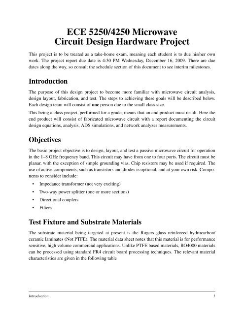
<strong>ECE</strong> <strong>5250</strong>/<strong>4250</strong> <strong>Microwave</strong> <strong>Circuit</strong> <strong>Design</strong> <strong>Hardware</strong> <strong>Project</strong>Table 1: RO4000® series materials available at Advance <strong>Circuit</strong>s (www.4pcb.com).Type Nominal er Loss Tangenttan RO4003CRO4350BFor circuitdesign 3.55Proc. Spec3.380.05@ 10 GHzFor circuitdesign 3.66Proc. Spec3.480.05@ 10 GHz0.0021 @ 2.5 GHz0.0027 @ 10 GHz0.0031 @ 2.5 GHz0.0037 @ 10 GHzSubstrate Thickness20 milother sizes:32 mil60 mil20 milother sizes:30 mil60 milFoilThickness0.5 oz0.5 ozThe test fixture layouts, come in two sizes. One being 3 inches square and the other being 3 by 6inches. The details are given in the following drawings:SMA withflat tab0.25"2-56Small TestFixtureFigure 1: The 3” by 3” test fixture.Test Fixture and Substrate Materials 2
<strong>ECE</strong> <strong>5250</strong>/<strong>4250</strong> <strong>Microwave</strong> <strong>Circuit</strong> <strong>Design</strong> <strong>Hardware</strong> <strong>Project</strong>SMA withflat tab0.25"2-56Large TestFixtureFigure 2: The 3” by 6” test fixture.An alternate fixture configuration, which does not use a mounting plate but does use the sameboard sizes for compatibility with the panel size, is to simply attach SMA connectors directly tothe pc board. With this configuration you can take your project with you. A low-cost connectorthat has been used in the past is the Pasternack Enterprises PE44206 of Figure 3. The RF/microwaveperformance of this edge connector has not been researched. In theory EMDA could be usedto model this connector along with the planar microwave circuit.Test Fixture and Substrate Materials 3
<strong>ECE</strong> <strong>5250</strong>/<strong>4250</strong> <strong>Microwave</strong> <strong>Circuit</strong> <strong>Design</strong> <strong>Hardware</strong> <strong>Project</strong>Figure 3: Pasternack PE44206 mechanical details.ScheduleThe design project will proceed in stages, with the final report due at the end of the semester. Themilestones are itemized below:• A brief description of the proposed design including preliminary ADS artwork and/or filesis due by no later than Monday November 16, 2009.• <strong>Project</strong> comments and final approval will be given during class on Wednesday November18. The next step is to fine tune your ADS layout file. A copy of your ADS layout (likely aGerber file) is due by no later than Monday November 24. The circuits will be sent out forfab Tuesday November 24.• Assembly and test will occur starting December 3 and through the last week of classes(December 7–11). Your measurement data should be incorporated into a re-work of yourADS model in an attempt to rationalize your hardware measurements. This can be thoughtof as a form or reverse engineering your design based on say actual physical measurementsof your circuit, etc.• On Wednesday December 16 a Final project report is due.Schedule 4