Altera DE2 Board Pin Table - DCE FEL ÄVUT v Praze
Altera DE2 Board Pin Table - DCE FEL ÄVUT v Praze
Altera DE2 Board Pin Table - DCE FEL ÄVUT v Praze

You also want an ePaper? Increase the reach of your titles
YUMPU automatically turns print PDFs into web optimized ePapers that Google loves.
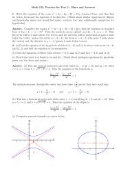
<strong>Altera</strong> <strong>DE2</strong> <strong>Board</strong> <strong>Pin</strong> <strong>Table</strong>LEDR[2] PIN_AB21 LED Red[2]LEDR[3] PIN_AC22 LED Red[3]LEDR[4] PIN_AD22 LED Red[4]LEDR[5] PIN_AD23 LED Red[5]LEDR[6] PIN_AD21 LED Red[6]LEDR[7] PIN_AC21 LED Red[7]LEDR[8] PIN_AA14 LED Red[8]LEDR[9] PIN_Y13 LED Red[9]LEDR[10] PIN_AA13 LED Red[10]LEDR[11] PIN_AC14 LED Red[11]LEDR[12] PIN_AD15 LED Red[12]LEDR[13] PIN_AE15 LED Red[13]LEDR[14] PIN_AF13 LED Red[14]LEDR[15] PIN_AE13 LED Red[15]LEDR[16] PIN_AE12 LED Red[16]LEDR[17] PIN_AD12 LED Red[17]LEDG[0] PIN_AE22 LED Green[0]LEDG[1] PIN_AF22 LED Green[1]LEDG[2] PIN_W19 LED Green[2]LEDG[3] PIN_V18 LED Green[3]LEDG[4] PIN_U18 LED Green[4]LEDG[5] PIN_U17 LED Green[5]LEDG[6] PIN_AA20 LED Green[6]LEDG[7] PIN_Y18 LED Green[7]LEDG[8] PIN_Y12 LED Green[8]Signal Name FPGA <strong>Pin</strong> No. DescriptionCLOCK_27 PIN_D13 On <strong>Board</strong> 27 MHz, <strong>Pin</strong>_C4 must be high to enableCLOCK_50 PIN_N2 On <strong>Board</strong> 50 MHzEXT_CLOCK PIN_P26 External ClockSignal Name FPGA <strong>Pin</strong> No. DescriptionUART_RXD PIN_C25 UART ReceiverUART_TXD PIN_B25 UART TransmitterSignal Name FPGA <strong>Pin</strong> No. DescriptionPS2_CLK PIN_D26 PS2 DataPS2_DAT PIN_C24 PS2 ClockSignal Name FPGA <strong>Pin</strong> No. DescriptionI2C_SCLK PIN_A6 I2C DataI2C_SDAT PIN_B6 I2C ClockSignal Name FPGA <strong>Pin</strong> No. DescriptionTD_DATA[0] PIN_J9 TV Decoder Data[0]TD_DATA[1] PIN_E8 TV Decoder Data[1]TD_DATA[2] PIN_H8 TV Decoder Data[2]TD_DATA[3] PIN_H10 TV Decoder Data[3]TD_DATA[4] PIN_G9 TV Decoder Data[4]TD_DATA[5] PIN_F9 TV Decoder Data[5]TD_DATA[6] PIN_D7 TV Decoder Data[6]TD_DATA[7] PIN_C7 TV Decoder Data[7]TD_HS PIN_D5 TV Decoder H_SYNCTD_VS PIN_K9 TV Decoder V_SYNCTD_RESET PIN_C4 TV Decoder ResetSignal Name FPGA <strong>Pin</strong> No. DescriptionVGA_R[0] PIN_C8 VGA Red[0]VGA_R[1] PIN_F10 VGA Red[1]VGA_R[2] PIN_G10 VGA Red[2]VGA_R[3] PIN_D9 VGA Red[3]VGA_R[4] PIN_C9 VGA Red[4]VGA_R[5] PIN_A8 VGA Red[5]VGA_R[6] PIN_H11 VGA Red[6]VGA_R[7] PIN_H12 VGA Red[7]VGA_R[8] PIN_F11 VGA Red[8]VGA_R[9] PIN_E10 VGA Red[9]VGA_G[0] PIN_B9 VGA Green[0]VGA_G[1] PIN_A9 VGA Green[1]VGA_G[2] PIN_C10 VGA Green[2]