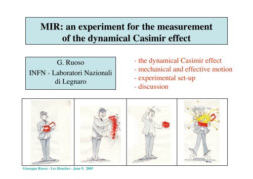
an experiment for the measurement of the dynamical Casimir effect
an experiment for the measurement of the dynamical Casimir effect
an experiment for the measurement of the dynamical Casimir effect
- No tags were found...

Create successful ePaper yourself
Turn your PDF publications into a flip-book with our unique Google optimized e-Paper software.
Surface mech<strong>an</strong>ical motionStrong limitation <strong>for</strong> a moving layer: INERTIA€δxE = 1 2 ρVω 2 δx 2ω / 2 π = 10 GHzδx > 1 nmMech<strong>an</strong>ical powerP ~ kW - MWTo be tr<strong>an</strong>sferred @ 10 GHzVery inefficient technique: to move <strong>the</strong> electrons giving <strong>the</strong> reflectivityone has to move also <strong>the</strong> nuclei with large waste <strong>of</strong> energyAlso, problems with <strong>the</strong> mech<strong>an</strong>ical designInstead <strong>of</strong> moving <strong>the</strong> complete layer one c<strong>an</strong> produce oscillations on <strong>the</strong>surfaces. Maximum de<strong>for</strong>mations be<strong>for</strong>e damage δ = ω a / v s , v s sound velocityGiuseppe Ruoso - Les Houches - June 9, 2005Maximum boundary velocity ~ 50 m/s
How to produce high frequency motioni) Acoustic waves in solidsIn <strong>the</strong> 60’s Bömmel-Dr<strong>an</strong>sfeldproduced GHz acoustic waves inquartz using piezo excitation, butexciting all modes. Motion <strong>of</strong> asingle mode δx
Surface <strong>effect</strong>ive motionV<strong>an</strong> der Walls <strong>for</strong>cesmeasured at µm dist<strong>an</strong>ces onsilicon sample ch<strong>an</strong>ge underillumination <strong>of</strong> <strong>the</strong> sampleParametric excitation <strong>of</strong> e.m.waves using a dense plasma layerin a cavity; <strong>the</strong> layer is created byirradiating a semiconductor filmwith femtosecond laser pulsesUse <strong>of</strong> laser pulse onsemiconductor to ch<strong>an</strong>ge veryrapidly its index <strong>of</strong> refractionGiuseppe Ruoso - Les Houches - June 9, 2005
Surface <strong>effect</strong>ive motion IIGenerate periodic motion by placing <strong>the</strong> reflecting surface intwo distinct positions alternativelyPosition 1 - metallic platePosition 2 - microwave mirror with driven reflectivityMetalplateVariablemirrorMicrowaveUSEP1 P2Semiconductors under illumination c<strong>an</strong> ch<strong>an</strong>ge <strong>the</strong>ir dielectric properties <strong>an</strong>d becomefrom completely tr<strong>an</strong>sparent to completely reflective <strong>for</strong> microwaves.Light with photon energyhν > E b<strong>an</strong>d gap <strong>of</strong> semiconductorEnh<strong>an</strong>ces electron density in <strong>the</strong> conduction b<strong>an</strong>dLaser ON - OFFOn semiconductorTime variable mirrorGiuseppe Ruoso - Les Houches - June 9, 2005
MIR - <strong>the</strong> <strong>experiment</strong>al schemeA semiconductor layer (thickness ~ 1 mm)is placed on one end <strong>of</strong> a niobium superconductingcavity. Cavity reson<strong>an</strong>ce ν r.Using <strong>an</strong> amplitude modulated (at frequencyf) laser light <strong>the</strong> semiconductorswitches from tr<strong>an</strong>sparency to reflection,thus producing <strong>an</strong> <strong>effect</strong>ive motion.whenf = 2 ν rPhotons will be produced in <strong>the</strong> vacuum<strong>an</strong>d will be picked-up by <strong>the</strong> <strong>an</strong>tennaWith this set-up <strong>the</strong> amplitude <strong>of</strong><strong>the</strong> motion in very large, thusproviding a large <strong>effect</strong>ive velocityΔT = 100 psT = 1 µs..n = 1 , 2 , 3 , 4, ... . , 10 3P las = 10 nJ/100 psGiuseppe Ruoso - Les Houches - June 9, 2005
Experimental issuesEffective mirror• <strong>the</strong> semiconductor when illuminated behavesas a metal (in <strong>the</strong> microwave b<strong>an</strong>d)• timing <strong>of</strong> <strong>the</strong> generation <strong>an</strong>d recombinationprocesses• quality factor <strong>of</strong> <strong>the</strong> cavity with insertedsemiconductor• possible noise coming fromgeneration/recombination <strong>of</strong> carriersLaser system• possibility <strong>of</strong> high frequencyswitching• pulse energy > threshold <strong>for</strong>complete reflectivity• number <strong>of</strong> consecutive pulsesDetection system• minimum detectable signal• noise from blackbodyradiationGiuseppe Ruoso - Les Houches - June 9, 2005
Semiconductor as a reflectorReflection curves <strong>for</strong> Si <strong>an</strong>d CuLight pulseExperimental set-upResults:• Perfect reflectivity <strong>for</strong> microwave Si, GaAs: R=1;• Light energy to make a good mirror ≈ 1 µJ/cm 2Time (µs)Giuseppe Ruoso - Les Houches - June 9, 2005
Timing <strong>of</strong> <strong>the</strong> reflection processIs it feasible to make <strong>the</strong> mirror appear <strong>an</strong>d disappear at GHz frequencies?mirror appear<strong>an</strong>cerise time <strong>of</strong> <strong>the</strong> laser pulse(e¯ tr<strong>an</strong>sition time ≈ fs)mirror disappear<strong>an</strong>cerecombination time <strong>of</strong> e¯property <strong>of</strong> <strong>the</strong> semiconductorτ needed is 20-40 psLow Temperature Grown GaAsGiuseppe Ruoso - Les Houches - June 9, 2005
Cavity with semiconductor wallComputer model <strong>of</strong>a cavity with asemiconductorwafer on a wallFundamental mode TE 101: <strong>the</strong> electric field Ea = 7.2 cmb = 2.2 cml = 11.2 cm=c2⎛ 1 ⎞⎜ ⎟⎝ a ⎠2⎛1⎞+ ⎜ ⎟⎝ l ⎠2f rQ L = πντ measured ≈ 3 · 10 6≅ 2.4899 GHzGiuseppe Ruoso - Les Houches - June 9, 2005600 µm thick slab <strong>of</strong> GaAs
Detection electronicsMinimum detectable signal inside <strong>the</strong> cavity
Detection electronics 2• Per<strong>for</strong>med a sensitivity <strong>measurement</strong> feeding a test signalP in=10 -12 dBm = 10 -15 W Δt = 1.6 µsE RF pulse=10 -15 J/s × 1.6 10 -6 s = 1.6 × 10 -21 J = 10 -2 eV ⇒10 3 RF photonsOscilloscope averagingafter 100 sweeps:• Measured <strong>the</strong> cavity output when flashing <strong>the</strong> ligth on <strong>the</strong>semiconductor --> NO signal detected --> NO noise inducedby <strong>the</strong> plasmaGiuseppe Ruoso - Les Houches - June 9, 2005
Laser systemPulsed laser with rep rate 5 GHz, pulse energy ~10 µJ, train<strong>of</strong> 10 3 - 10 4 pulses, slightly frequency tunable ~ 800 nmLaser master oscillator5 GHz, low powerPulse pickerOptical amplifierTotal number <strong>of</strong> pulses limited by <strong>the</strong>energy available in <strong>the</strong> opticalamplifier: good estimate 1000-5000(Total energy 10 - 50 mJ)Each train repeated every few secondsGiuseppe Ruoso - Les Houches - June 9, 2005
Detailed set-upWorking temperature4 - 9 KComplete freeze out <strong>of</strong>carriers insemiconductorNo background noisefrom <strong>the</strong>rmal photonsCavity reson<strong>an</strong>ce in <strong>the</strong>r<strong>an</strong>ge 2 - 3 GHzSemiconductorthickness ~ 1 mmGiuseppe Ruoso - Les Houches - June 9, 2005
Giuseppe Ruoso - Les Houches - June 9, 2005The apparatus
Giuseppe Ruoso - Les Houches - June 9, 2005Inside <strong>the</strong> cryostat
Detection schemeN pulsesSteps5. Look <strong>for</strong> signal with τ ~ Q / 2πν r1. Find cavity frequency ν r2. Wait <strong>for</strong> empty cavity3. Set laser system to 2 ν r4. Send burst with > 1000 pulsest p= 1/ 2 ν rCharged cavity.Will decay with itstime const<strong>an</strong>tExpected number <strong>of</strong> photons:Niobium cavity with TE 101 ν r = 2.5 GHz (22 x 71 x 110 mm 3 )Semiconductor GaAs with thickness δx = 0.6 mmSingle run with ~ 5000 pulsesN ≥ 10 4 photonsGiuseppe Ruoso - Les Houches - June 9, 2005
Check listSeveral things c<strong>an</strong> be employed to disent<strong>an</strong>gle a real signal from aspurious oneSignal (a.u.)Ch<strong>an</strong>ge temperature <strong>of</strong> cavityEffect on black body photonsCh<strong>an</strong>ge laser pulse rep. frequency1.61.41.210.80.60.85 0.9 0.95 1 1.05 1.1Laser pulse frequency (a.u)Loading <strong>of</strong> cavity with real photons (isour system a microwave amplifier?)Power inside cavity at end <strong>of</strong> laser pulses (a.u.)14121086420Determine vacuum <strong>effect</strong> from several<strong>measurement</strong>s with pre-loaded cavity0 1 2 3 4 5 6Power inside cavity at t = t0 (a.u.)-ch<strong>an</strong>ge recombination time <strong>of</strong> semiconductor-ch<strong>an</strong>ge width <strong>of</strong> semiconductor layerGiuseppe Ruoso - Les Houches - June 9, 2005
ConclusionThe <strong>experiment</strong> MIR seems feasibleFinish R & D within 1 year• complete laser system with high power part• develop a system to characterize semiconductors (autocorrelation)Giuseppe Ruoso - Les Houches - June 9, 2005