Dual-Mode Capacitive Proximity Sensor for Robot Application ...
Dual-Mode Capacitive Proximity Sensor for Robot Application ...
Dual-Mode Capacitive Proximity Sensor for Robot Application ...

Create successful ePaper yourself
Turn your PDF publications into a flip-book with our unique Google optimized e-Paper software.
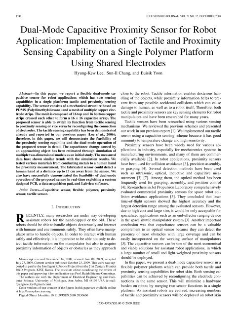
LEE et al.: DUAL-MODE CAPACITIVE PROXIMITY SENSOR FOR ROBOT APPLICATION 1749Fig. 2. (a) Structure of a tactile cell consisting of five layers. (b) Cross-sectionview of a tactile cell.Fig. 1. Conceptual diagram of the proposed dual mode tactile sensor. (a) Deployedon a robot arm. (b) On a robot hand.in a large area <strong>for</strong> dexterous and safe operation. Minimizinghardware burden will be one of the serious issues in deployingsensors in terms of pay load in weight, volume, and number ofdevices. By switching operation modes (tactile and proximitymodes), we can monitor proximity and tactile in<strong>for</strong>mation of anobject as it approaches to and touches on the sensor. Since thetactile sensing capability of the proposed sensor was reportedin our previous paper [1], in this paper, proximity sensing capabilityand dual-mode operation of the implemented proximitysensor will be described in detail.II. SENSOR STRUCTURE AND OPERATION PRINCIPLEFig. 1 illustrates the conceptual diagram of the proposed dualmodesensor. Each sensor has a modular structure and can beconnected through interconnection lines to <strong>for</strong>m an extendedsensor array <strong>for</strong> large-area coverage, as shown in Fig. 1(a). Inthe proximity mode, the sensor detects an approaching objectwithin a detectable range by using a fringing electric field. In thetactile mode, the sensor captures the contact <strong>for</strong>ce distributioninduced by a physical contact of the object. The sensor is ableto monitor both proximity and tactile in<strong>for</strong>mation by switchingbetween the two modes as it is required. Fig. 1(b) illustrates anotherexample of possible applications <strong>for</strong> robot hands or manipulators<strong>for</strong> grasping an object. The control of manipulatorcan be more accurate and safer by using both sensors together.The structure of the proposed dual-mode sensor is shown inFig. 2. The sensor consists of a 16 16 array of unit cells. Acell is composed of five Polydimethylsiloxane (PDMS) layers.Copper electrodes are embedded in the PDMS layers. Two electrodes(top and bottom electrodes) <strong>for</strong>m a capacitor <strong>for</strong> tactilesensing, separated by total ( by air and by aninsulation layer, respectively). The cell size isand the capacitor size is, respectively. Thecell pitch is 1 mm. Initial capacitance of a cell has been estimatedas 171 fF, assuming the relative permittivity of PDMS as2.75 given by product datasheet (Sylgard 184, Dow Corning).When a contact pressure is applied to a bump, the upper PDMSlayer de<strong>for</strong>ms and capacitance increases until the air gap is completelyclosed.Fig. 3(a) shows the electrode configuration of the proposedsensor. The 16 16 array sensor has the total 16 strips in the topelectrodes and another 16 strips in the bottom electrodes. Thetop and bottom copper strips are crossing each other to <strong>for</strong>m acell capacitor which can be addressed individually. The conceptof operation of each mode is depicted in Fig. 3(b) and (c). Thetop 16 strips are reconfigured to select either tactile or proximityoperation. In the proximity mode [Fig. 3(b)], the fringing capacitancebetween the two groups of the top electrodes is monitored.In the tactile mode [Fig. 3(c)], the capacitance betweenthe top and bottom electrodes in a cell is measured. The whole16 16 array is scanned to acquire a tactile image.The sensor has been fabricated by bonding five separatepolymer layers, as shown in Fig. 2(a): a bump layer, upperand lower electrode layers, an insulation layer, and a spacerlayer. Each layer is <strong>for</strong>med by vulcanizing liquid PDMS on acarrier silicon wafer. Copper electrodes are <strong>for</strong>med using electroplating.The fabrication process of the sensor is explained
1750 IEEE SENSORS JOURNAL, VOL. 9, NO. 12, DECEMBER 2009Fig. 5. Two different top electrode configurations tested <strong>for</strong> proximity modeoperation.Fig. 3. Principle of dual mode operation of the proposed capacitive sensorarray. (a) The mesh structure of top and bottom metal electrodes. (b) <strong>Proximity</strong>mode operation by detecting a fringe capacitance change in the top electrodesfrom an approaching object. (c) Tactile mode operation by measuring the capacitancechange in each tactile cell induced by physical contact of the object.Fig. 6. Diagram describing division of the electrode structure <strong>for</strong> two-dimensionalsimulation models. (a) Plain view of top and bottom electrodes of fourtactile cells showing three parts of a different cross section in a cell. (b) Thecross-section of each part.III. PROXIMITY SENSING EXPERIMENTFig. 4. (a) Fabricated dual mode tactile sensor array. (b) Magnified view closeto tactile cell array.in detail in our previous paper [1]. Fig. 4 shows the completedtactile sensor reported previously [1].A. Simulation of the <strong>Proximity</strong> Sensing Capability of theFabricated <strong>Sensor</strong>Since the fabricated sensor has the 16 strips of top electrodes,there exist many possible variations of the electrode configurationto generate a fringing electric field. Among them, we chosetwo extreme configurations in this work to compare the effect ofthe number of fringes. We also tested different status of bottomelectrodes: floating and grounded (fixed potential). Fig. 5 illustratesthe two top electrode configurations. Type A is a combelectrode structure which has fifteen fringes consisting of alternateelectrode strips. Type B has only one fringe which consistsof two large electrodes (eight strips per electrode). The potentialof bottom electrodes is floating <strong>for</strong> both configurations.Type B’, which is not shown in the figure, has grounded bottomelectrodes while the top electrode configuration is same withType B.
LEE et al.: DUAL-MODE CAPACITIVE PROXIMITY SENSOR FOR ROBOT APPLICATION 1751Fig. 7. The simulated two-dimensional map of electric potential (0 1V)and equipotential lines from every part of type A, B, and B configuration.TABLE IINITIAL CAPACITANCE VALUES AND CAPACITANCE CHANGES WITH RESPECT TO THE DISTANCE TO THE OBJECT OBTAINED FROM THE SIMULATIONFor quick simulation of the proximity sensing capability ofthe sensor with limited resources, we estimated three-dimensionalsensor response by combining simulation results frommultiple two-dimensional models. Fig. 6 describes two-dimensionalmodels we used <strong>for</strong> simulation. Fig. 6(a) shows the plainview of a portion of top and bottom electrode array. We dividedthe sensor into three parts depending on their cross sections.Fig. 6(b) displays the cross sections of three parts. Part 1is in the middle of the tactile cell area which has bottom electrodesin both cell and interconnection area. The width of Part 1is 0.2 mm. Part 2 is comprised of top and bottom electrodes ofsame size in the cell area, which has total 0.2 mm width. Part 3is between cell areas which consist of narrow top electrodes tointerconnect each tactile cell. Part 3 has 0.6 mm width as shownin the figure. The PDMS structure also has been modeled aroundthe top and bottom electrodes. The gap between top and bottomelectrodes is determined as and filled with PDMS in themodel, which is electrically similar to the real structure, in orderto reduce the complexity of the model. The capacitance value ofeach part has been simulated using FEM software (COMSOL3.2b). The total capacitance value of the sensor has been calculatedby summing up the contribution from each part assumingthat the discontinuity between parts would not affect the totalcapacitance much. The whole 16 16 array was included inthe calculation. The approaching object has been assumed asa grounded metal.Fig. 7 displays the map of electric potential and equipotentiallines of each part in every configuration obtained by simulation.The potential varies from 0 to 1 V. The simulated initial capacitancevalues of Type A, B, and B’ are 16.6, 14.5, and 0.4 pF,respectively. The simulated capacitance change from the initialvalue as a function of the distance to the approaching object hasbeen summarized in Table I. The “SUM” column contains thetotal capacitance change that is the sum of other columns. Thedata in Table I have been visualized and compared in Fig. 8.Each graph displays the capacitance change of Part 1, 2, 3, andthe whole sensor (the sum of part 1, 2, and 3), respectively.One of the significant observations is that the initial capacitanceis dominated by Part 1 and 2, while the capacitance changeis dominated by Part 3 when the potential of the bottom electrodeis floating. The contribution of Part 3 to the total capacitancechange is the greatest though the contribution to the initialcapacitance is the least among three parts. The reason <strong>for</strong> largeinitial capacitance in Part 1 and 2 is that most of the electricflux from the positive top electrodes goes to the top negativeelectrodes through the floating bottom electrodes since the gap
1752 IEEE SENSORS JOURNAL, VOL. 9, NO. 12, DECEMBER 2009Fig. 8. Simulated capacitance change as a function of the distance to the object from (a) Part 1, (b) Part 2, (c) Part 3, and (d) the whole sensor.between top and bottom electrodes are much smallerthan that between top electrodes. The larger capacitancechange in Part 3 is because its width is three timesbigger than Part 1 and 2. Part 1 and Part 2 show slightly biggerchanges than Part 3 if the capacitance change normalized withtheir width is compared. However, Part 3 exhibits the largestcapacitance change compared to its initial capacitance whichmeans the highest sensitivity.Another important observation is that the capacitance changeof the two types is almost same at a far distance as shown inFig. 8 though Type A shows larger capacitance change thanType B in all parts at a close distance due to larger numberof fringes. Part 3 exhibits the largest difference between TypeA and B at a close distance, as displayed in Fig. 8(c). Part 2is between Part 1 and Part 3. As a result, the total capacitancechange of the sensor also exhibits the same behavior, as shownin Fig. 8(d). It seems from the result that the number of fringingcapacitance affects on the sensitivity at a close distance but noton the maximum detectable distance which depends on the minimumdetectable capacitance change. The maximum detectabledistance is almost same <strong>for</strong> both types. In a system perspective,Type B is more desirable configuration owing to its smaller initialcapacitance value.The comparison between Type B and Type B’ is also shown inFig. 8(d). If the bottom electrode is fixed to the ground or otherpotentials, little electric flux from the positive top electrode goesto the negative top electrode because the bottom electrode connectedto an external source consumes most of flux in Part 1 andPart 2. There<strong>for</strong>e, both of the initial capacitance and the capacitancechange drop significantly, so that they are much smallerFig. 9. Schematic diagram of the proximity sensing circuit.than other types as shown in Table I and Fig. 8(d). The maximumdetectable distance of Type B’ is also inferior to that ofType A and B.B. Measurement of the <strong>Proximity</strong> Sensing Capability of theFabricated <strong>Sensor</strong>The proximity sensing capability of the fabricated sensor hasbeen measured using a simple charge amplifier circuit and a digitallock-in amplifier <strong>for</strong> low-noise measurement, as illustratedin Fig. 9. A 250 kHz sinusoidal signal has been used to operatethe sensor. In order to block any parasitic electric fields fromthe backside of the sensor, a shielding plate which is fixed to thereference voltage (2.5 V) through a buffer was placedbelow the sensing electrodes as shown in the figure. An aluminumplate ofhas been used as anapproaching object.
LEE et al.: DUAL-MODE CAPACITIVE PROXIMITY SENSOR FOR ROBOT APPLICATION 1753Fig. 10. (a) Measurement results of capacitance change from all the configurations. (b)–(d) Comparison between simulation and measurement data from Type A,B, and B’.TABLE IISIMULATION AND MEASUREMENT DATA OF INITIAL CAPACITANCE ANDCAPACITANCE CHANGE FROM EACH SENSOR CONFIGURATIONThe measurement data have been summarized in Table II. Thegraphs in Fig. 10 display the measured capacitance change alongwith the simulation results <strong>for</strong> comparison. They exhibit similartrends we expected through simulation. The measured initial capacitanceof Type A, B, and B’ are 13.1, 8.6, and 0.2 pF, respectively.As observed in the simulation, Type A has the largerinitial capacitance and capacitance change at a close distancethan Type B, as shown in Fig. 10(a). However, the measured capacitancechange of Type B at a far distance is slightly biggerthan Type A which is different from the simulation though thedifference is subtle. This might be caused by the measurementenvironment. Since the sensor is sensitive to the electric field, itis easily affected by parasitic signals from the measurement environment.We have also observed some signal drift from timeto time during the experiment. A more rigorous experiment ina well-shielded environment will be needed to characterize thesensor more accurately. This will be addressed in our next work.The measurement data of Type B’ are much smaller than thoseof Type A and B as expected in simulation.In general, the measurement data of initial capacitance valueand capacitance change at a far distance are much smaller thanthe simulation data. This discrepancy comes from the approximativemodeling we used <strong>for</strong> simulation. The shielding plateplaced 10 mm under the sensor which is not modeled in simulationalso might affect significantly. At a close distance, themeasurement data show higher capacitance change than simulationin Type A and B. It seems that this is from the inefficientmesh used <strong>for</strong> simulation. The measurement data show abruptchange in a distance range shorter than 2 cm. A well-definedfine mesh structure in this range would provide more accuratesimulation results. However, the simulation provided us reasonabledata to predict the sensor behavior in advance.In order to compare proximity signals from various materials,we tested metals, plastics, and other dielectrics such as copper,steel, PVC, Acrylic, HDPE, glass, wood, and ceramic. All thematerials have the same size as in the aluminum sample that weused in our previous measurement. Fig. 11 displays the capacitancechange measured by the various materials as a function ofapproaching distance. While metals produce almost the same response,dielectrics show wide variations. Interestingly, this variationdoes not have any correlation with the dielectric properties(e.g., relative permittivity). We initially expected that the capacitancechange would depend on dielectric constant. However, theresults were quite the opposite. It seems that there are surfacecharges on the surface of dielectric materials and this affects the
1754 IEEE SENSORS JOURNAL, VOL. 9, NO. 12, DECEMBER 2009Fig. 11.Comparison of measurement data from different materials.Fig. 12. Block diagram of the implemented sensor system <strong>for</strong> dual-modeoperation.electric field generated by the sensor. We are currently workingon this issue to understand the cause of this phenomenon. Formetals, however, we observed reproducible responses. We alsomeasured the proximity of a human hand as shown in the figure.The signal from the hand was larger than metals because the sizeof a hand including a wrist is bigger than metal samples usedin the experiment. The maximum detectable distance has beenmeasured as large as 17 cm <strong>for</strong> the hand.IV. DUAL-MODE OPERATIONFor dual mode operation, we integrated the readout circuits<strong>for</strong> both operation modes (proximity and tactile) with analogswitch matrices in a PCB. Fig. 12 shows the block diagramof our prototype system. Analog switches connect sensor electrodesto either tactile or proximity readout circuits accordingto the control signals from a controller. The controller implementedusing a field programmable gate array (FPGA) generatestiming control and switching signals. Function generatorand data acquisition pad from National Instruments are connectedto the prototype system. The data acquisition pad providespower to the PCB. It also sends a few handshaking controlsignals including synchronization, and receives the proximityand tactile data from the PCB.Fig. 13. Photographs of the implemented sensor system demonstrating dualmodeoperation displaying: (a) <strong>Proximity</strong> mode operation to monitor the distanceof a finger from the sensor; (b) Switching mode from proximity to tactilesensing mode when the finger touches the sensor; and (c) Tactile mode operationto display real-time images of contact <strong>for</strong>ce applied to the sensor by the finger.In the proximity sensing mode, the left half of the total 16 topelectrode strips is connected to an external function generatorand the right half is connected through a signal amplifier to thedata acquisition pad by the column switch array. All the lowerelectrodes are connected to a reference voltage by the rowswitch array to provide ac ground. In the tactile sensing mode,the upper and lower electrodes are connected to the column androw decoders by the analog switch arrays, respectively, <strong>for</strong> scanningtactile images.Labview software is used to control the automatic switchingbetween the two modes. Normally, the sensor is operating inproximity sensing mode and continuously monitoring the distanceto approaching objects. Once the approaching object iswithin the preset threshold level of proximity signal, the systemis switched to the tactile sensing mode and begins to readout tactilein<strong>for</strong>mation. The sensor measures both tactile and proximitysignals by switching each mode alternately in order to monitorthe detachment of the object from the sensor. When the objectmoves away from the sensor beyond the threshold, the sensorsystem returns to the proximity sensing mode. Fig. 13 displays
LEE et al.: DUAL-MODE CAPACITIVE PROXIMITY SENSOR FOR ROBOT APPLICATION 1755the operation of the prototype system <strong>for</strong> an approaching humanfinger. The measured proximity and tactile signals are transmittedto the data acquisition pad and displayed on a laptopcomputer by Labview software. There are two display images;the left one shows the contact <strong>for</strong>ce distribution (tactile image)and the right one displays proximity in<strong>for</strong>mation, respectively.As the finger approaches, the distance in the proximity gaugedecreases, as shown in Fig. 12(a). When the finger touches thesensor, as shown in Fig. 12(b), the proximity gauge displays zeroand the sensor switches its mode to the tactile sensing mode.Then, the measured contact <strong>for</strong>ce distribution appears on the tactiledisplay in the screen (Fig. 12(c)). When the finger leaves thesensor, the proximity mode takes over the operation again.V. CONCLUSIONIn this paper, we have successfully demonstrated the feasibilityof a flexible dual-mode capacitive sensor <strong>for</strong> robot applicationswhich has two sensing capabilities in a single plat<strong>for</strong>m;tactile and proximity sensing capability. The sensor consists oftwo layers of 16 16 electrode arrays embedded in a siliconerubber (PDMS) structure. The electrode array is composed of 16top copper strips and 16 bottom copper strips crossed each otherto <strong>for</strong>m a 16 16 capacitor array. In this paper, the proximitysensing capability of the proposed sensor has been simulatedand evaluated through an experiment. We characterized the per<strong>for</strong>manceof proximity measurement <strong>for</strong> various materials includingmetals, plastics, glass, wood, and a human hand. Thesensor could detect the proximity of a human hand up to 17 cmaway from the sensor. We also demonstrated switching betweentwo modes in real-time by exploiting a custom circuit board withLabview software. The proposed dual-mode sensor will be anattractive option <strong>for</strong> robot applications because it provides twoessential sensing functions in a single plat<strong>for</strong>m mitigating thehardware burden required <strong>for</strong> multiple sensor deployment.REFERENCES[1] H.-K. Lee, S.-I. Chang, and E. Yoon, “A flexible polymer tactilesensor: Fabrication and modular expandability <strong>for</strong> large area deployment,”ASME/IEEE J. Microelectromech., vol. 15, pp. 1681–1686,Dec. 2006.[2] R. C. Ruo, “<strong>Sensor</strong> technologies and microsensor issues <strong>for</strong> mechatronicssystems,” IEEE/ASME Trans. Mechatron., vol. 1, no. 3, pp.39–49, 1996.[3] R. Volpe and R. Ivlev, “A survey and experimental evaluation of proximitysensors <strong>for</strong> space robots,” in Proc. IEEE Int. Conf. <strong>Robot</strong>. Autom.,1994, vol. 4, pp. 3466–3473.[4] A. Bonen, R. E. Saad, K. C. Smith, and B. Benhabib, “A novelelectrooptical proximity sensor <strong>for</strong> robotics: Calibration and activesensing,” IEEE Trans. <strong>Robot</strong>. Autom., vol. 13, pp. 377–386, Mar. 1997.[5] S. Hongo, K. Nakamura, and N. Hosokawa, “<strong>Proximity</strong> sensors utilizingan evanescent acoustic field <strong>for</strong>med by flexural plate waves,” inProc. Ultrasonics Symp., 1997, vol. 1, pp. 475–478.[6] K. Koibuchi, K. Sawa, T. Honma, T. Hayashi, K. Ueda, and H. Sasaki,“Loss estimation and sensing property enhancement <strong>for</strong> eddy-currenttypeproximity sensor,” IEEE Trans. Magn., vol. 42, pp. 1447–1450,Apr. 2006.[7] Z. Chen and R. C. Ruo, “Design and implementation of capacitiveproximity sensor using microelectromechanical systems technology,”IEEE Trans. Ind. Electron., vol. 45, pp. 886–894, Dec. 1998.[8] J. L. Novak and I. T. Feddema, “A capacitive-based proximity sensor<strong>for</strong> whole arm obstacle avoidance,” in Proc. IEEE Int. Conf. <strong>Robot</strong>.Autom., 1992, pp. 1307–1314.[9] H.-K. Lee, S.-I. Chang, and E. Yoon, “A capacitive proximity sensor indual implementation with tactile imaging capability on a single flexibleplat<strong>for</strong>m <strong>for</strong> robot assistant applications,” in Proc. IEEE MEMS Conf.,2006, pp. 606–609.Hyung-Kew Lee received the B.S. degree and theM.S. degree in electrical engineering from the KoreaAdvanced Institute of Science and Technology(KAIST), Daejeon, Korea, in 1996 and 1999, respectively.He worked on uncooled infrared bolometers<strong>for</strong> his M.S. thesis. He received the Ph.D. degreefrom KAIST in 2004 <strong>for</strong> the research about a tunableoptical filter.He joined the University of Minnesota in 2005as a Postdoctoral Research Scholar and worked ontactile devices <strong>for</strong> robots and mobile handsets. He iscurrently working at Seagate Technology in Minnesota. His primary researchinterests are tactile interface system, flexible electronics, microsystems,and photonics.Sun-Il Chang received the B.S. degree in electricalengineering from Korea University, Seoul, in 2003.He is currently working towards the Ph.D. degree atthe Department of Electrical Engineering and ComputerScience, University of Michigan, Ann Arbor.He worked on a tactile sensor readout systemat the Korea Advanced Institute of Science andTechnology (KAIST). His current research interestis in smart sensor system design with low noise andpower readout.Euisik Yoon received the B.S. and M.S. degrees inelectronics engineering from Seoul National University,Seoul, Korea, in 1982 and 1984, respectively,and the Ph.D. degree in electrical engineering fromthe University of Michigan, Ann Arbor, in 1990.From 1990 to 1994, he worked <strong>for</strong> the FairchildResearch Center of the National Semiconductor Corporation,Santa Clara, CA, where he engaged in researchingdeep submicron CMOS integration and advancedgate dielectrics. From 1994 to 1996, he wasa Member of the Technical Staff at Silicon GraphicsInc., Mountain View, CA, where he worked on the design of the MIPS microprocessorR4300i and the RCP 3-D graphic coprocessor. He took faculty positionsin the Department of Electrical Engineering, Korea Advanced Instituteof Science and Technology (KAIST), Daejeon, Korea, from 1996 to 2005, andin the Department of Electrical and Computer Engineering, University of Minnesota,Minneapolis, from 2005 to 2008, respectively. During the academic yearof 2000 to 2001, he was a Visiting Faculty at Agilent Laboratory, Palo Alto, CA.In 2008, he joined the Department of Electrical Engineering and Computer Science,University of Michigan, Ann Arbor. His research interests are in MEMS,integrated microsystems, and VLSI circuit design.Dr. Yoon was the co-recipient of the Student Paper Award at the IEEE InternationalMicrowave Symposium in 1999 and 2000, respectively, concerningthe topics on MEMS inductors and RF MEMS switch work. He has servedon various Technical Program Committees including the Microprocesses andNanotechnology Conference, the International <strong>Sensor</strong> Conference, the IEEE APASIC Conference, the IEEE MEMS Conference and Transducers Conference.He also served on the IEEE ISSCC Program Committee and currently is servingon the IEEE IEDM Executive Committee.