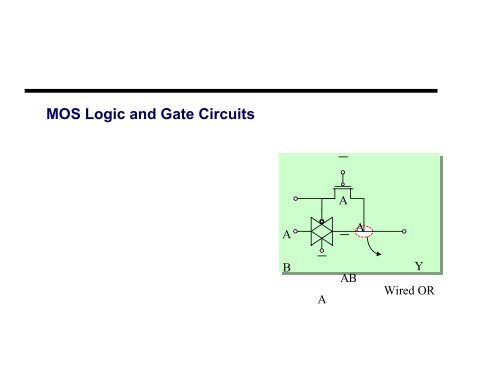
MOS Logic and Gate Circuits
MOS Logic and Gate Circuits
MOS Logic and Gate Circuits

Create successful ePaper yourself
Turn your PDF publications into a flip-book with our unique Google optimized e-Paper software.
<strong>MOS</strong> <strong>Logic</strong> <strong>and</strong> <strong>Gate</strong> <strong>Circuits</strong>AAABAABYWired OR
ContentsIntroductionN<strong>MOS</strong> <strong>Logic</strong>Resistive LoadSaturated Enhancement LoadLinear Enhancement LoadDepletion LoadSome <strong>Gate</strong>sTransient in N<strong>MOS</strong> CircuitPseudo-N<strong>MOS</strong>C<strong>MOS</strong> <strong>Logic</strong>Static C<strong>MOS</strong> <strong>Logic</strong> <strong>Gate</strong>s• NOT• NAND• NOR• Realization of More Complicated <strong>Gate</strong> <strong>Circuits</strong>Transmission <strong>Gate</strong>s Family• N<strong>MOS</strong> Only Switch• C<strong>MOS</strong>Differential Cascode Voltage Switch <strong>Logic</strong>Rules of ThumbSummary
IntroductionThe <strong>MOS</strong> inverter is the basic circuit exhibits all of theessential features of <strong>MOS</strong> <strong>Logic</strong>. Extension of <strong>MOS</strong> inverterconcepts to NOR <strong>and</strong> NAND <strong>Gate</strong> is very simple. In thislecture we will analysis for VTC, NM, PD,… . Both N<strong>MOS</strong><strong>and</strong> C<strong>MOS</strong> circuits are considered. Digital <strong>MOS</strong> circuits canbe classified into two categories: Static <strong>Circuits</strong>: require no clock or other periodic signal foroperation. Clocks are required for static circuit in sequentiallogic Dynamic <strong>Circuits</strong>: require periodic clock signals, synchronizedwith data signals, for proper operation even in combinationallogic
N<strong>MOS</strong> <strong>Logic</strong>Resistive Load⎛ W ⎞⎜ VoL C SpeedL⎟ ↑⇒ ↓⇒ ↑⇒ ↓⎝ ⎠P↓⇒ RL↑⇒ Area ↑VoVddVi+VddRLVoV OLoVi
N<strong>MOS</strong> <strong>Logic</strong>Resistive Load Properties N transistors + Load V OH= Vdd V OL= Vdd ( rN/(rN + RL)) Assymetrical response Static power consumption t PL= 0.69RLCL
N<strong>MOS</strong> <strong>Logic</strong>Saturated Enhancement LoadVds2 = Vgs2 ⇒+ Vdd + VddVds2 > Vgs2 −V⇒VoV OHδVoδVi= −1T2M2 is in saturationViM2M1Vo∝β RV OLoV ILViV IH
N<strong>MOS</strong> <strong>Logic</strong>Saturated Enhancement Load V ILV ≥V ⇒ M1, M2 are in saturationILT1⇒ K(Vgs1− V ) = K(Vgs2−V ),V ≈Cte2 21 T1 2 T2δVoVgs1 = Vi, Vgs2 = Vdd −Vo ⇒ = − βR, βR> 1δViδVo⇒ ≠ −1⇒ VI L≈ VT1δViT2VoV OHV OLoδVoδViV ILV IH= −1∝ β RVi
N<strong>MOS</strong> <strong>Logic</strong>Saturated Enhancement Load V OL• V OL is difficult to obtainbecause it is the outputvoltage when input equal toV OH , the resulting expressionis a fourth order polynomial!VoV OHδVoδVi= −1∝ β RV OLoV ILViV IH
N<strong>MOS</strong> <strong>Logic</strong>Saturated Enhancement Load V IH• M1 is in triode <strong>and</strong> M2 in saturationδVoδi1=−δViδViδVords1 rds2 ≈ rds1 = δ i( rds1 rds2)( )⎡⎣1i2 = K2(Vgs2−V T2)2δiKVo1δVi2i1 = K1 Vgs1−VT1Vo−Vo 21⇒ =12⎤⎦δiδVoK ( Vgs1 V Vo)δVoKVoδVi K (Vgs1 −V −Vo)1⇒ =1−T1−1⇒ =− = −⇒ Vo =Vi − V2V1 T1T1− VIH T1Vi = VIH⇒ = Vo21
N<strong>MOS</strong> <strong>Logic</strong>Saturated Enhancement Load V IH• M1 is in triode <strong>and</strong> M2 in saturationi= i ⇒1 21K ⎡⎣( V −V ) Vo− Vo 2⎤⎦= K (Vdd−Vo−V )22(Vdd − V )VT13β + 12 21 IH T1 2 T2T2⇒ VIH= +R
N<strong>MOS</strong> <strong>Logic</strong>Saturated Enhancement Load NMNML = V −V ≈Some tenth of voltILOLNMH = V − V = Vdd −V −VOH IH T2 IH PowerP ≈ 0, P = I VdddisH disL d⇒ P = 1 2I Vdddisd
N<strong>MOS</strong> <strong>Logic</strong>Linear Enhancement LoadVGG ≥ Vdd + V T2⇒ M2 is in triodeLinear Enhancement LoadVGGVi+VddM2VoM1
N<strong>MOS</strong> <strong>Logic</strong>Linear Enhancement Load VTC• By this circuit the V OHcan be increased (or Vddcan be decreasedbecause Vo max = Vdd )VoVddV OLoV ILVddViV TV IH
N<strong>MOS</strong> <strong>Logic</strong>Linear Enhancement Load V IL• M1 is in saturation <strong>and</strong> M2 in triodeδVoδi1 δi1δVds2=− rds2 =−δVi δVi δVi δi( )⎣⎡⎤⎦δi2= K2( VGG −Vo −VT2δVds2−Vds2)2i2 = K2 Vgs2 −VT2Vds2 −Vds2 2112i1 = K1(Vi−V T1)2δi1= K1( Vi−VT1)δViδVo−K(Vi 1−V T1)=− 1 =δVi K (VGG −Vo −V −Vds2)⇒ V = f(Vo)IL2 T2 V IH• M1 <strong>and</strong> M2 are in trioderds2 → rds1 rds2
N<strong>MOS</strong> <strong>Logic</strong>Linear Enhancement Load Disadvantages:• More chip area is required (since an extra voltage source VGG)• Additional interconnection on the chip is neededβ R• The required value of is even larger than a saturated load+VddVGGM2VoViM1
N<strong>MOS</strong> <strong>Logic</strong> Depletion Load Ion implantation processing step is needed to createdepletion device, but overcome the disadvantages ofthe previous circuit+VddM2VoViM1
N<strong>MOS</strong> <strong>Logic</strong> Depletion Load VTCVi = Low ⇒ i = 0, M1 in cutoff ⇒ i = i = 01 1 2K22if M2 is in saturation then i2= (Vgs2 − VT2) ,Vgs2 = 0 ⇒ i2> 02 Therefore M2 is in triodeVoVddV OLoV ILV TV IHVddVi
N<strong>MOS</strong> <strong>Logic</strong> Depletion Load V OL , V IL , V IH2 K22K ⎡1⎣( VOH −VT1)VOL − VOL 2 ⎤⎦= (0−V T2) ⇒ VOL= ?2δVoK(Vgs1−V )=− ⇒ =− = ⇒ =δVi K (Vgs2 −V −Vds2)1 T11 1, i1 i2 VIL?2 T22 K22 δVoi1 = K ⎡1⎣( VIH −VT1)Vds1− Vds1 2⎤⎦= i2= (0− VT2) , =−1⇒ VIH= ?2 δVi
N<strong>MOS</strong> <strong>Logic</strong> Some <strong>Gate</strong>s In all previous structures which different only in load,the following <strong>Gate</strong>s can be implemented. Note that theN<strong>MOS</strong> <strong>Gate</strong>s are not available as separately packagedindividual circuits, but they are used extensively in LSIsystems• NOR <strong>Gate</strong>s• NAND <strong>Gate</strong>s
N<strong>MOS</strong> <strong>Logic</strong> Some <strong>Gate</strong>s NOR <strong>Gate</strong>+VddAM1BRLM2YABY
N<strong>MOS</strong> <strong>Logic</strong> Some <strong>Gate</strong>s NAND <strong>Gate</strong>+VddARLM2YABYBM1
N<strong>MOS</strong> <strong>Logic</strong> Some <strong>Gate</strong>s In NOR <strong>Gate</strong> two transistors are paralleled but inNAND <strong>Gate</strong> two transistors are in series. Because ofthe need for increased area when adding NAND inputs,NAND logic with more than 2 inputs is noteconomically be attractive in N<strong>MOS</strong>. NOR logic ispreferable In NAND the M2 has body effect In NOR we need the less interconnection (this can beshown from layout)
N<strong>MOS</strong> <strong>Logic</strong>Transient in N<strong>MOS</strong> <strong>Circuits</strong> Saturated Enhancement Load+VddM2Cgs2Cgd1+VddCs − sub2CLVoViM1Cd − sub1C = C + Ceq + Ceq + Cgs2 + 2×Cgd1tot L d−sub1 s−sub2
N<strong>MOS</strong> <strong>Logic</strong> Super Buffer (1)If Fan-out is very large thenC tot will be large. Forreduction it <strong>and</strong> decrease theswitching time the SuperBuffer circuit is usedIn this circuit if Vi is Lowstate then V1 will be highvery more rapid than Vo.Thus the <strong>Gate</strong> of M2 is inhigh state very rapidly.Therefore M2 will be insaturation which result thereduction of switching time(t on )+Vdd +VddM4M2V1VoM1M3ViSuper Buffer (1) Circuit
N<strong>MOS</strong> <strong>Logic</strong> Super Buffer (2) It is non-Inverting Describe the operation ofthis circuit!M4+Vdd+VddM2ViV1M1M3VoSuper Buffer (2) Circuit
N<strong>MOS</strong> <strong>Logic</strong>Pseudo-N<strong>MOS</strong> What makes a circuit fast?• I = C dV/dt -> tpd ∝ (C/I) DV• low capacitance• high current• small swing <strong>Logic</strong>al effort is proportional to C/I P<strong>MOS</strong> are the enemy!• High capacitance for a given current Can we take the P<strong>MOS</strong> capacitance off the input? Various circuit families try to do this…
N<strong>MOS</strong> <strong>Logic</strong>Pseudo-N<strong>MOS</strong> In the old days, N<strong>MOS</strong> processes had no P<strong>MOS</strong>• Instead, use pull-up transistor that is always ON In C<strong>MOS</strong>, use a P<strong>MOS</strong> that is always ON• Make P<strong>MOS</strong> about ¼ effective strength of pulldownnetwork
N<strong>MOS</strong> <strong>Logic</strong>Pseudo-N<strong>MOS</strong> Uses a p-type as a resistive pullup, n-type network forpulldowns+VddM2VoViM1
N<strong>MOS</strong> <strong>Logic</strong>Pseudo-N<strong>MOS</strong> Characteristics Compared to C<strong>MOS</strong>, thisfamily has higher packingdensity, since for n inputs onlyn+1 transistors are required The main disadvantages withPseudo-N<strong>MOS</strong> <strong>Gate</strong>s is thelarge static power dissipationthat occurs whenever a pulldownpath is activated Has much smaller pullupnetwork than static gate Pulldown time is longerbecause pullup is fightingVi+VddM2VoM1
N<strong>MOS</strong> <strong>Logic</strong>Pseudo-N<strong>MOS</strong> Output Voltages <strong>Logic</strong> 1 output is always at Vdd <strong>Logic</strong> 0 output is above Vss V OL= 0.25 (Vdd - Vss) is oneplausible choice+VddM2VoViM1
N<strong>MOS</strong> <strong>Logic</strong>Pseudo-N<strong>MOS</strong> Design Topics For logic 0 output, pullup <strong>and</strong>pulldown form a voltage divider Must choose n, p transistorsizes to create effectiveresistances of the requiredratio Effective resistance ofpulldown network must becomputed in worst case—series n-types means largertransistorsVi+VddM2VoM1
N<strong>MOS</strong> <strong>Logic</strong>Pseudo-N<strong>MOS</strong> Transistor Ratio Calculation <strong>MOS</strong>FET sizing is important Need to have reasonable W/L ratios for circuit to workcorrectly V OL>VSS but must be low enough to turn off/on next<strong>MOS</strong>FET in the chain Static current drain when “on” Vout is a function of the number of parallel <strong>and</strong> series Nchannels in the pull down network
N<strong>MOS</strong> <strong>Logic</strong>Pseudo-N<strong>MOS</strong> Transistor Ratio CalculationFor single supplyVOH= Vdd, For the worst case one N<strong>MOS</strong> to be on2⎡V ⎤ KK ⎢ Vdd V V Vdd V⎣2 ⎦ 2OL P( − ) − ⎥ = ( − )n Tn OL TP⎡ KV = K (Vdd−V ) ⎢1− 1−K⎣OL n T 2⎢nAssuming that V = V = VV →0⇒ K
N<strong>MOS</strong> <strong>Logic</strong> Pseudo-N<strong>MOS</strong> VTC ( W/L n =1)3.02.52.0W/L p = 4V out[V]1.51.0W/L p= 20.5W/L p= 0.5W/L p = 0.25W/L p= 10.00.0 0.5 1.0 1.5 2.0 2.5V in[V]
N<strong>MOS</strong> <strong>Logic</strong>Pseudo-N<strong>MOS</strong> <strong>Gate</strong>s Design for unit current on output P<strong>MOS</strong> fights N<strong>MOS</strong>inputsfY
N<strong>MOS</strong> <strong>Logic</strong>Pseudo-N<strong>MOS</strong> Power Pseudo-N<strong>MOS</strong> draws power whenever Y = 0• Called static power P = I•VDD• A few mA / gate * 1M gates would be a problem• This is why N<strong>MOS</strong> went extinct! Use Pseudo-N<strong>MOS</strong> sparingly for wide NORs Turn off P<strong>MOS</strong> when not in useenABCY
N<strong>MOS</strong> <strong>Logic</strong>Pseudo-N<strong>MOS</strong> ( NAND) Layout ExampleOutIn1 In2 In3 In4
C<strong>MOS</strong> <strong>Logic</strong> Static C<strong>MOS</strong> <strong>Logic</strong> Family All of the circuits described in the previous sectionshave a large static power dissipation. Thisdisadvantage can be overcome by using Static C<strong>MOS</strong><strong>Logic</strong> Family
C<strong>MOS</strong> <strong>Logic</strong> Static C<strong>MOS</strong> <strong>Logic</strong> Family NOT+VddViM2M1Vo
C<strong>MOS</strong> <strong>Logic</strong> Static C<strong>MOS</strong> <strong>Logic</strong> Family Two inputs NAND+VddM3M4YBM2AM1
C<strong>MOS</strong> <strong>Logic</strong> Static C<strong>MOS</strong> <strong>Logic</strong> Family Two inputs NOR+VddABY
C<strong>MOS</strong> <strong>Logic</strong> Static C<strong>MOS</strong> <strong>Logic</strong> Family NAND is more suitable for C<strong>MOS</strong> because by supposethe equal W/L for N<strong>MOS</strong> <strong>and</strong> P<strong>MOS</strong> transistors, theP<strong>MOS</strong> transistor has more resistance respect toN<strong>MOS</strong>, therefore it is better to design circuit byparalleling the P<strong>MOS</strong> <strong>and</strong> cascading the N<strong>MOS</strong> The better Technology for digital circuit is N-Well,because in this Technology the N<strong>MOS</strong> transistors aremade in the Sub. Which result better characteristic fortransistor
C<strong>MOS</strong> <strong>Logic</strong>Realization of More Complicated <strong>Gate</strong> <strong>Circuits</strong> a) Y = A(B+C) It can be implemented in three levels:• <strong>Gate</strong> Level• Transistor Level• Layout Level
C<strong>MOS</strong> <strong>Logic</strong>Realization of More Complicated <strong>Gate</strong> <strong>Circuits</strong> a) Y = A(B+C)• <strong>Gate</strong> Level– It consists of 10 transistors, 4 transistors for NOR, 2 for NOT <strong>and</strong> 4 forNANDBCAY
C<strong>MOS</strong> <strong>Logic</strong>Realization of More Complicated <strong>Gate</strong> <strong>Circuits</strong> a) Y = A(B+C)• Transistor Level– It need only 6 transistorsAB+VddCYABC
C<strong>MOS</strong> <strong>Logic</strong>Realization of More Complicated <strong>Gate</strong> <strong>Circuits</strong> a) Y = A(B+C)• Layout Level– By proper construction of layout, the parasitic capacitors are alsoreduced <strong>and</strong> area can be saved
C<strong>MOS</strong> <strong>Logic</strong>Realization of More Complicated <strong>Gate</strong> <strong>Circuits</strong> b) XNOR (Y = AB + AB)• <strong>Gate</strong> Level– 16 transistors are neededAYB
C<strong>MOS</strong> <strong>Logic</strong>Realization of More Complicated <strong>Gate</strong> <strong>Circuits</strong> b) XNOR (Y = AB + AB)• Transistor Level (1)» How many transistors are» needed?+VddABBAY = AB+ABBBAA
C<strong>MOS</strong> <strong>Logic</strong>Realization of More Complicated <strong>Gate</strong> <strong>Circuits</strong> b) XNOR• Transistor Level (2)– Previous circuit can besimplified by eliminatingtwo wiring linesAB+VddBAY = AB+ABBABA
C<strong>MOS</strong> <strong>Logic</strong>Realization of More Complicated <strong>Gate</strong> <strong>Circuits</strong> b) XNOR• Transistor Level (3)– In this circuit we havestatic power dissipationin the state of (A=0,B=1)or (A=1,B=0)+VddM3Y = AB+ABM1M2AB
C<strong>MOS</strong> <strong>Logic</strong>Realization of More Complicated <strong>Gate</strong> <strong>Circuits</strong> b) XNOR• Transistor Level (4) (For less dissipation)– Note to the state of A = B = VddABY+Vdd000VddVdd0M4M3Y = AB+ABVdd00M1M2VddVddVdd-VthAB
C<strong>MOS</strong> <strong>Logic</strong>Realization of More Complicated <strong>Gate</strong> <strong>Circuits</strong> c) XOR• As Previous the Source <strong>and</strong> Drain of M3 (or M4) arereplaced by each other in different states, for example instate of A=0, B=0 the b connection of M3 is SourceABY+ Vdd000VddVthVdd-VthAM2BaM3Y = AB+ABa b bVdd0VddM1M4VddVdd0A
C<strong>MOS</strong> <strong>Logic</strong>Realization of More Complicated <strong>Gate</strong> <strong>Circuits</strong> d) Tri-State Outputs• A floating state at the output is needed– Non-Inverting⎧En = 1 ⇒ Y = D⎨⎩En = 0 ⇒ Y = Hi −ZEn+VddDEnYDY
C<strong>MOS</strong> <strong>Logic</strong>Realization of More Complicated <strong>Gate</strong> <strong>Circuits</strong> d) Tri-State Outputs• A floating state at the output is needed– Inverting⎧⎪ En = 1 ⇒ Y = Hi −Z⎨⎪⎩ En = 0 ⇒ Y = DD YEnEn+VddYD
C<strong>MOS</strong> <strong>Logic</strong>Realization of More Complicated<strong>Gate</strong> <strong>Circuits</strong> e) Schmitt Trigger• M3 <strong>and</strong> M6 have minimum sizedgeometries• With Vin = 0 , the transistors M1 <strong>and</strong>M2 will be on but conductingnegligible Drain current since M4<strong>and</strong> M5 are offVinVxVy+VddM1M3M2Y⇒Vy ≈Vx ≈ VddM4Vy ≈ Vdd ⇒M6 ≅on ⇒ Vz = Vy −VTNVzM6M5+Vdd
C<strong>MOS</strong> <strong>Logic</strong>Realization of More Complicated<strong>Gate</strong> <strong>Circuits</strong> e) Schmitt Trigger• When Vin rise to V TN, M5 turns on,but M4 is off. M5 <strong>and</strong> M6 form anN<strong>MOS</strong> amplifier. Thus as Vin rises,Vz is falling <strong>and</strong> in the certainvoltage M4 turns on. With both M4<strong>and</strong> M5 conducting, Vy rapidly goesto zero turning off M6. With Vy=0, M3turns on, which aids in turning offM2 as Vx goes from Vdd to Vy-V TP• As Vin decrease from Vdd to zerothe operation is essentially similar.But now M1 turns on, in differentvoltage <strong>and</strong> …VinVxVyVz+VddM1M3M2M4M6M5Y+Vdd
C<strong>MOS</strong> <strong>Logic</strong>Transmission <strong>Gate</strong>s Family Use pass transistors like switches to do logic Inputs drive diffusion terminals as well as gates N transistors instead of 2N No static power consumption Ratioless Bidirectional
C<strong>MOS</strong> <strong>Logic</strong>Transmission <strong>Gate</strong>s Family N<strong>MOS</strong> Only SwitchVddXIn3.0InVoltage [V]2.01.0Outx0.00 0.5 1 1.5 2Time [ns]
C<strong>MOS</strong> <strong>Logic</strong>Transmission <strong>Gate</strong>s FamilyN<strong>MOS</strong> Only Switch• V Bdoes not pull up to 2.5V, but 2.5-V TN• Threshold voltage loss causes (M 2may be weaklyconducting forming a path from Vdd to GND)• N<strong>MOS</strong> has higher threshold than P<strong>MOS</strong> (body effect)
C<strong>MOS</strong> <strong>Logic</strong>Transmission <strong>Gate</strong>s FamilyN<strong>MOS</strong> Only Switch• Pass transistor gates should never be cascaded as onthe left• <strong>Logic</strong> on the right suffers from static power dissipation<strong>and</strong> reduced noise margins
C<strong>MOS</strong> <strong>Logic</strong>Transmission <strong>Gate</strong>s Family N<strong>MOS</strong> Only Switch• Solution1: Level Restoring TransistorLevel RestorerBV ddM rV ddM 2AMnXOutM 1
C<strong>MOS</strong> <strong>Logic</strong>Transmission <strong>Gate</strong>s FamilyN<strong>MOS</strong> Only Switch• Solution1: Level Restoring TransistorAdvantages• Full swing on x (due to Level Restorer) so no static powerconsumption by inverter• No static backward current path through Level Restorer <strong>and</strong> PTsince Restorer is only active when A is high• Restorer adds capacitance, takes away pull down current at XFor correct operation Mr must be sized correctly (ratioed)
C<strong>MOS</strong> <strong>Logic</strong>Transmission <strong>Gate</strong>s Family N<strong>MOS</strong> Only Switch• Solution2: Multiple V T Transistorslow V TtransistorsIn 2 = 0VA= 2.5VonOutIn 1 = 2.5Voff butleakingB= 0Vsneak path
C<strong>MOS</strong> <strong>Logic</strong>Transmission <strong>Gate</strong>s FamilyN<strong>MOS</strong> Only Switch• Solution2: Multiple V T Transistors Technology solution: Use (near) zero V Tdevices for theN<strong>MOS</strong> TGs to eliminate most of the threshold drop (bodyeffect still in force preventing full swing to Vdd) Impacts static power consumption due to subthresholdcurrents flowing through the TGs (even if VGS is below V T)In 2 = 0VA= 2.5Vonlow V TtransistorsOutIn 1 = 2.5Voff butleakingB= 0Vsneak path
C<strong>MOS</strong> <strong>Logic</strong> Transmission <strong>Gate</strong>s Family N<strong>MOS</strong> Only Switch• Disadvantage:– It can be bad because the signal can be degraded– We do not allow a few gates in series for one signal (Pure TG logicis not regenerative, the signal gradually degrades after passingthrough a number of TGs)• Advantage:– Allow us to save transistor or less stage of logicAZB
C<strong>MOS</strong> <strong>Logic</strong> C<strong>MOS</strong> Transmission <strong>Gate</strong>s Family P<strong>MOS</strong>AYC C<strong>MOS</strong>CCAYAYCC
C<strong>MOS</strong> <strong>Logic</strong>C<strong>MOS</strong> Transmission <strong>Gate</strong>s Family There are many symbols for transmission gateBBBAZAZAZORB'BOOKB'MEAB'Z Be careful, because it is bi-directional
C<strong>MOS</strong> <strong>Logic</strong>C<strong>MOS</strong> Transmission <strong>Gate</strong>s FamilyThis circuit performs a function similar to that of the well known diode bridgeC = Vss, C = 0 ⇒ Both transistor are on ⇒ A = YThe input voltage VA (which must be between Vss <strong>and</strong> Vdd) is thenconnected to the output through the parallel on resistance of the channels ofthe two transistors. As VA approaches Vdd, the N-channel device cuts off butthe P-channel device remains non saturated, as VA approaches Vss, the P-channel device cuts off but the N-channel device remains non saturated.Therefore there is always a non saturated transistor between input <strong>and</strong> outputCCA YA YCC
C<strong>MOS</strong> <strong>Logic</strong>C<strong>MOS</strong> Transmission <strong>Gate</strong>s Family For more underst<strong>and</strong>ing note to this circuit We assume:−Vy(0 ) = 0, C = Vdd, C = 0, V < Vdd −VTPTNVACVddVyASDI PI NYCLtC
C<strong>MOS</strong> <strong>Logic</strong>C<strong>MOS</strong> Transmission <strong>Gate</strong>s Family⎧N= sat0 ≤ t ≤ t ⇒ I I IVy=V⎨ ⇒ = +TP⎩P= satCL N P⎧N= satt ≤ t ≤ t ⇒ rVy VPCL= TPVy= Vdd−V⎨ ⇒τ≈TN⎩P= triode⎧N= offt ≤ t ≤ t ⇒ rVy Vdd VPCL= − TNVy=Vdd⎨ ⇒τ≈⎩P= triodeACI PI NCYCL
C<strong>MOS</strong> <strong>Logic</strong>C<strong>MOS</strong> Transmission <strong>Gate</strong>s Family It is normally assumed as a resistorV (t)A=Vddu(t)C⎡ ⎛ −t⎞⎤Vy(t) = Vdd ⎢1 −exp⎜⎟⎥u(t)⎢⎣⎝τTG⎠⎥⎦τ = R CLTGTGR = r rTG N PAI PI NCYCL
C<strong>MOS</strong> <strong>Logic</strong>C<strong>MOS</strong> Transmission <strong>Gate</strong>s Family r N<strong>and</strong> r Pare approximately as follow (In saturation region)rrANN 2N(Vdd − VTN)APP 2P(Vdd − VTP)A≈ β≈ β2V2VV is Early VoltageRrPVTPRTG = rN rPr NVdd − VTNVddVy
C<strong>MOS</strong> <strong>Logic</strong>C<strong>MOS</strong> Transmission <strong>Gate</strong>s Family What to note about TG• The inputs must be able to give high current because they areconnected directly to Drain <strong>and</strong> Source of transistors• Since each input is connected to an RC circuit, The delay canbe considered directly• Limited Fan-in• Excessive Fan-out• Noise vulnerability (not restoring)• Supply voltage offset/bias vulnerability• Poor high voltage levels if N<strong>MOS</strong>-only• Body effect
C<strong>MOS</strong> <strong>Logic</strong>C<strong>MOS</strong> Transmission <strong>Gate</strong>s FamilyRules of Thumb• Pass-<strong>Logic</strong> may consume half the power of static logic. But becareful of V T drop resulting in static leakage• Pass-<strong>Gate</strong> <strong>Logic</strong> is not appropriate when long interconnectsseparate logic stages or when circuits have high Fan-out load(use buffering)
C<strong>MOS</strong> <strong>Logic</strong>C<strong>MOS</strong> Transmission <strong>Gate</strong>s FamilyAND
C<strong>MOS</strong> <strong>Logic</strong>C<strong>MOS</strong> Transmission <strong>Gate</strong>s Family ORY = A+ AB = (A+ A)(A+ B) = A+BAAABAABYWired OR
C<strong>MOS</strong> <strong>Logic</strong>C<strong>MOS</strong> Transmission <strong>Gate</strong>s Family MUX⎧A S = 1Y = ⎨⎩B S = 0SABSYS
C<strong>MOS</strong> <strong>Logic</strong>C<strong>MOS</strong> Transmission <strong>Gate</strong>s Family MUXF = (In1S+In2S)S S FV ddIn 1 In 2GNDSS
C<strong>MOS</strong> <strong>Logic</strong>C<strong>MOS</strong> Transmission <strong>Gate</strong>s Family XORBABY = A⊕BB
C<strong>MOS</strong> <strong>Logic</strong>C<strong>MOS</strong> Transmission <strong>Gate</strong>s Family XNORBABY = AB+ABB
C<strong>MOS</strong> <strong>Logic</strong>C<strong>MOS</strong> Transmission <strong>Gate</strong>s Family D Latch1) Load Q = D2) Hold Q = Qnnn n-1DLDQQLDDLDLDQLD
C<strong>MOS</strong> <strong>Logic</strong>C<strong>MOS</strong> Transmission <strong>Gate</strong>s Family D Latch1) Load LD = 1D Q = DD=Q2) Hold LD = 0QQ
C<strong>MOS</strong> <strong>Logic</strong>C<strong>MOS</strong> Transmission <strong>Gate</strong>s Family D Latch (Simpler Realization)• If in Load Mode a level voltage opposite to the output of weakinverter is applied to the input by TG, Q = D <strong>and</strong> weak inverteris not damaged!LDDQLDQWeak Inverter
C<strong>MOS</strong> <strong>Logic</strong> Delay in Transmission <strong>Gate</strong>InV1V2ViVi + 1V n−1C C C C C CV nInReqRV eq1V2ReqV eq eqiVi + 1V n−1C C C C C CRRReqV nInm644474448ReqReqReqReqReqReqC C C C C C
C<strong>MOS</strong> <strong>Logic</strong>Delay Optimization Delay of RC chainn∑t = 0.69 C R k = 0.69C RP eq eqk=1 Delay of Buffered chainn(n + 1)2⎡ n m(m+1) ⎤ ⎛ n ⎞tP= 0.69 ⎢ C Re q1 tbufm 2⎥+ ⎜ −m⎟⎣ ⎦ ⎝ ⎠⎡ n(m + 1) ⎤ ⎛ n ⎞= 0.69 ⎢C Re q1 tbuf2⎥+ ⎜ −m⎟⎣ ⎦ ⎝ ⎠tPbufmopt= 1.7 CReq
C<strong>MOS</strong> <strong>Logic</strong>TG Points to Remember Stored charge leaks away due to reverse-bias leakagecurrent Stored value is good for about 1 ms Value must be rewritten to be valid If not loaded every cycle, must ensure that latch isloaded often enough to keep data valid Capacitance comes primarily from inverter’s gate logic
C<strong>MOS</strong> <strong>Logic</strong>TG Layout
C<strong>MOS</strong> <strong>Logic</strong>TG Properties Strong pull-up Strong pull-down May be difficult to design into a circuit (layout) becauseof close proximity of N <strong>and</strong> P devices (design ruleseparation) Always requires 2N transisitors for any N x TG design Many logic functions (multiplexers in particular) areeasily implemented using TG based designs
C<strong>MOS</strong> <strong>Logic</strong>Complementary Pass-transistor <strong>Logic</strong> (CPL) orDifferential (+) TG <strong>Logic</strong> Dual-rail form of pass transistor logic Avoids need for ratioed feedbackAABBAABBPT NetworkInverse PTNetworkFFFFABABSSSSLLYY
C<strong>MOS</strong> <strong>Logic</strong>CPLBBABABAND/NAND
C<strong>MOS</strong> <strong>Logic</strong>4 Input NAND in CPL
C<strong>MOS</strong> <strong>Logic</strong>CPL Advantages Differential so complementary data inputs <strong>and</strong> outputsare always available (so don’t need extra inverters) Still static, since the output defining nodes are alwaystied to Vdd or GND through a low resistance path Design is modular, all gates use the same topology,only the inputs are permuted Simple XOR makes it attractive for structures likeadders Fast (assuming number of transistors in series is small)
C<strong>MOS</strong> <strong>Logic</strong>CPL Disadvantages Additional routing overhead for complementary signals Still have static power dissipation problems V OH is very weak! Then we need an inverter at theoutput
C<strong>MOS</strong> <strong>Logic</strong>Differential Cascode Voltage Switch <strong>Logic</strong> (DCVSL)Compute both true <strong>and</strong> complementary outputs using a pair ofcomplementary N<strong>MOS</strong> pull-down network The P<strong>MOS</strong> transistors are driven by the output of thecomplementary network No static power consumption Fast responseYYInputsff
C<strong>MOS</strong> <strong>Logic</strong>Differential Cascode Voltage Switch <strong>Logic</strong> (DCVSL) Example: NAND/ANDY=ABY= A+BABA⎫⎬SeriesB⎭
C<strong>MOS</strong> <strong>Logic</strong>Differential Cascode Voltage Switch <strong>Logic</strong> (DCVSL) General DesignA00001111B00110011C01010101F10010111CBA0 1_+_+_+_+_+_+_+
C<strong>MOS</strong> <strong>Logic</strong>Differential Cascode Voltage Switch <strong>Logic</strong> (DCVSL) General Designababx_+≡xxx_+≡uu = ax+bxuuuabababx_+_+≡x_+u 1u 2u 1u 2
C<strong>MOS</strong> <strong>Logic</strong>Differential Cascode Voltage Switch <strong>Logic</strong> (DCVSL) General Design0 1C0 1_+_+_+_+C_+_+BA_+_+_+BA_+__++
C<strong>MOS</strong> <strong>Logic</strong>Differential Cascode Voltage Switch <strong>Logic</strong> (DCVSL) Example: XOR/XNOR
C<strong>MOS</strong> <strong>Logic</strong>Rules of ThumbStep-up (alpha) ratio of 2.7 (“e”) produces minimum powerdelayproductP vs. N (beta) ratio of 2 balances pull-up <strong>and</strong> pull-downtimes <strong>and</strong> noise marginsApproximately 75% of static logic are NAND stacks (limitstack to 3-4, use ordering <strong>and</strong> tapering for speed)Glitches consume approximately 15% of overall chip powerCrossover (short-circuit) current consumes ~ 10% of astatic chip’s total power (but is a function of input/outputslews, ie sizing)
Summary This lecture describes the basic <strong>MOS</strong> <strong>Logic</strong><strong>Gate</strong>s which require no clock or other periodicsignal for operation <strong>and</strong> also implementation ofthem in three following levels <strong>Gate</strong> Level Transistor level Layout Level
Contents Introduction Dynamic C<strong>MOS</strong> <strong>Logic</strong> C<strong>MOS</strong> Domino <strong>Logic</strong> CD Domino <strong>Logic</strong> Dynamic CVSL Sample-Set Differential <strong>Logic</strong> (SSDL) Summary
IntroductionAs mentioned before Digital <strong>MOS</strong> circuits can be classifiedinto two categories: Static <strong>Circuits</strong>: require no clock or other periodic signal foroperation (except sequential logic). In these circuits at everypoint in time (except when switching) the output is connectedto either GND or Vdd via a low resistance path fan-in of N requires 2N devices (n N-type + n P-type) Dynamic <strong>Circuits</strong>: require periodic clock signals, synchronizedwith data signals, for proper operation even in combinationallogic. These circuits rely on the temporary storage of signalvalues on the (parasitic) capacitance of high impedance nodes requires only N + 2 transistors (n+1 N-type + 1 P-type) takes a sequence of precharge <strong>and</strong> conditional evaluationphases to realize logic functions
IntroductionWhy Dynamic <strong>Logic</strong>?In the area of high speed, higher Fan-in, extremely lowpower dissipation, other digital logic circuit have beenconsidered. In this lecture, two of these alternatives toC<strong>MOS</strong> are described. The circuits are basically N<strong>MOS</strong> orC<strong>MOS</strong> <strong>Gate</strong>s with slight improvements. These are: Dynamic C<strong>MOS</strong> <strong>Logic</strong> C<strong>MOS</strong> Domino <strong>Logic</strong>Each of them have specific operating advantages overN<strong>MOS</strong> or C<strong>MOS</strong>, but exhibit disadvantages in other areas
Dynamic C<strong>MOS</strong> <strong>Logic</strong>Dynamic <strong>Gate</strong>s use a clocked P<strong>MOS</strong> pullupTwo modes: precharge <strong>and</strong> evaluateφ Precharge EvaluatePrechargeY
Dynamic C<strong>MOS</strong> <strong>Logic</strong>The Foot What if pulldown network is ON during precharge? Use series evaluation transistor to prevent fightφAYprecharge transistorfoot
Dynamic C<strong>MOS</strong> <strong>Logic</strong>Dynamic C<strong>MOS</strong> <strong>Logic</strong> To make the gate dynamic, aclock pulse is applied to the gateof complementary P <strong>and</strong> Nchannel devices. This gateconsists of an N<strong>MOS</strong> <strong>Logic</strong> circuitwhose output node is prechargedto Vdd by the P<strong>MOS</strong>, when theclock is zero. The output node isdischarged by the N<strong>MOS</strong>transistor connected to groundwhen the clock is highCLKP CLKN<strong>MOS</strong><strong>Logic</strong>CircuitN CLK
Dynamic C<strong>MOS</strong> <strong>Logic</strong>Dynamic C<strong>MOS</strong> <strong>Logic</strong>M p1L23M ePrecharge (Clk = 0)Evaluate (Clk = 1)
Dynamic C<strong>MOS</strong> <strong>Logic</strong>Once the output of a dynamic gate is discharged, it cannotbe charged again until the next precharge operationInputs to the gate can make at most one transition duringevaluationOutput can be in the high impedance state during <strong>and</strong> afterevaluation (PDN off), state is stored on C L
Dynamic C<strong>MOS</strong> <strong>Logic</strong>Canonical Forms
Dynamic C<strong>MOS</strong> <strong>Logic</strong>Properties of Dynamic <strong>Gate</strong>s <strong>Logic</strong> function is implemented by the PDN only• should be smaller in area than static complementary C<strong>MOS</strong> Full swing outputs (V OL= GND <strong>and</strong> V OH= V DD) Nonratioed - sizing of the devices is not important for properfunctioning (only for performance) Faster switching speeds• reduced load capacitance due to lower number of transistors pergate (C int ) so a reduced logical effort• reduced load capacitance due to smaller fan-out (C ext )• no I sc , so all the current provided by PDN goes into dischargingC L• Ignoring the influence of precharge time on the switching speedof the gate, t pLH = 0 but the presence of the evaluation transistorslows down the t pHL
Dynamic C<strong>MOS</strong> <strong>Logic</strong>Properties of Dynamic <strong>Gate</strong>s Power dissipation should be better• consumes only dynamic power – no short circuit powerconsumption since the pull-up path is not on when evaluating• lower C L - both C int (since there are fewer transistors connectedto the drain output) <strong>and</strong> C ext (since there the output load is oneper connected gate, not two) But power dissipation can be significantly higher due to• higher transition probabilities• extra load on CLK PDN starts to work as soon as the input signals exceed V Tn,so set V M, V IH<strong>and</strong> V ILall equal to V Tn• low noise margin (NM L ) Needs a precharge/evaluate clock
Dynamic C<strong>MOS</strong> <strong>Logic</strong>Leakage Sources Subthreshold conduction Transistors can’t abruptly turnON or OFF Reverse-biased PN junctiondiode current• I sdepends on doping levels And area<strong>and</strong> perimeter of diffusion regions,typically < 1 fA/µm 2 <strong>Gate</strong> Leakage• Carriers may tunnel thorough very thingate oxides• Negligible for older processes10 9 t ox10 6 V DD trend0. 6 nm0. 8 nm10 31. 0 nm1. 2 nm10 010 -310 -610 -90 0.3 0.6 0.9 1.2 1.5 1.8V DD1. 5 nm1. 9 nm
Dynamic C<strong>MOS</strong> <strong>Logic</strong>Leakage SourcesOutput settles to an intermediate voltage determined by a resistivedivider of the pull-up <strong>and</strong> pull-down networksOnce the output drops below the switching threshold of the fan-outlogic gate, the output is interpreted as a low voltage2.5CLKVoltage (V)1.50.5Out-0.50 20 40Time (ms)
Dynamic C<strong>MOS</strong> <strong>Logic</strong> Leakage Sources Subthreshold leakage is dominant in modern transistorsCLKpLeV OutPrechargeEvaluateLeakage sources
Dynamic C<strong>MOS</strong> <strong>Logic</strong> Solution to Charge LeakageM p M kpLM e
Dynamic C<strong>MOS</strong> <strong>Logic</strong>Charge SharingCharge stored originally on CY is redistributed (shared) over CXleading to static power consumption by downstream gates <strong>and</strong>possible circuit malfunctionWhen ∆Vout = - Vdd (CX / (CX + CY )) the drop in Vout is largeenough to be below the switching threshold of the gate it drivescausing a malfunctionφφAB = 0xC xxYC YYACharge sharing noiseCYV = V = VC + Cx Y ddx Y
Dynamic C<strong>MOS</strong> <strong>Logic</strong>Solution to Charge Redistribution Add secondary precharge transistors (at the cost ofincreased area <strong>and</strong> power)• Typically need to precharge every other node• Secondary precharge transistors should be small because theirdiffusion capacitance slows the evaluation (increase delay)• Big load capacitance C Y helps as wellABxYsecondaryprechargetransistor
Dynamic C<strong>MOS</strong> <strong>Logic</strong>Charge Sharing Example What is the worst case voltage drop on y? (Assume allinputs are low during precharge <strong>and</strong> that all internal nodesare initially at 0V)
Dynamic C<strong>MOS</strong> <strong>Logic</strong>Charge Sharing Example⎡⎣( a c) ( a c y)( ( ))∆ Vout = − Vdd C + C C + C + C=− 2.5V 30 30 + 50 =−0.94V⎤⎦CLKy = A B CLoadinverteraAAC y =50fFyC a =15fFB B BcbBdC b =15fFC c =15fFCCC d =10fFCLK
Dynamic C<strong>MOS</strong> <strong>Logic</strong> Backgate Coupling Susceptible to crosstalk due to• High impedance of the output node• Capacitive coupling– Out2 capacitively couples with Out1 through the gate-source <strong>and</strong> gatedraincapacitances of M4CLKA=0B=0CLKM pM 1M eC L1Out1 =1M 6M 2M 3M 4M 5C L2Out2 =0InDynamic NANDStatic NAND
Dynamic C<strong>MOS</strong> <strong>Logic</strong> Backgate Coupling Capacitive coupling means Out1 drops significantly so Out2doesn’t go all the way to ground3Due to clk feedthroughVoltage21ClkOut1Due to backgate0InOut2-10 2 4 6Time, ns
Dynamic C<strong>MOS</strong> <strong>Logic</strong> Clock Feedthrough A special case of capacitivecoupling between the clockinput of the precharge transistor<strong>and</strong> the dynamic output nodedue to the gate to draincapacitance So voltage of Out can rise aboveVdd. The fast rising (<strong>and</strong> fallingedges) of the clock couple toOutM pM eL
Dynamic C<strong>MOS</strong> <strong>Logic</strong> Clock FeedthroughClock feedthrough2.51.5Voltage0.5In &ClkOut-0.50 0.5 Time, ns 1Clock feedthrough
Dynamic C<strong>MOS</strong> <strong>Logic</strong> Other Effects Capacitive coupling Substrate coupling Minority charge injection Supply noise (Ground bounce) Floating output nodes
Dynamic C<strong>MOS</strong> <strong>Logic</strong> Floating output nodes Solutions:• Only connect to gates• Add staticizer to refresh the charges00s
Dynamic C<strong>MOS</strong> <strong>Logic</strong>Advantages:For n inputs, dynamic logic requiresn+2 transistorshave small area, high speed <strong>and</strong>compact layoutsCLKP CLKDisadvantages:Circuit operation is more complexdue to the required clockThe inputs can only change duringthe precharge phase <strong>and</strong> must bestable during the evaluate portion ofthe cycleN<strong>MOS</strong><strong>Logic</strong>CircuitN CLKNeed Monotonicity• can not be cascaded
Dynamic C<strong>MOS</strong> <strong>Logic</strong>Monotonicity Dynamic gates require monotonically rising inputsduring evaluationAviolates monotonicityduring evaluationφφ Precharge EvaluatePrechargeAYOutput should rise but does not
Dynamic C<strong>MOS</strong> <strong>Logic</strong>Monotonicity Woes Dynamic gates produce monotonically falling outputs duringevaluation Illegal for one dynamic gate to drive another!A 1 =PrechargeEvaluatePrechargeXX monotonically falls during evaluationYY should rise but cannot
Dynamic C<strong>MOS</strong> <strong>Logic</strong> CascadingVClkInOut1V TnOut2∆VOnly 0 → 1 transitions allowed at inputs!t
Dynamic C<strong>MOS</strong> <strong>Logic</strong> Cascading Input going from high to low during evaluation• a is 5V when precharge b = 5V, c = 5V• During evaluation:– Wanted: b 0V, c 5V– But, b takes some time to drop to 0V– Consequently, c may fall to some unknown value Solution NP-C<strong>MOS</strong> NORA <strong>Logic</strong> Domino logicabc
Dynamic C<strong>MOS</strong> <strong>Logic</strong> NP-C<strong>MOS</strong> Only 0 → 1 transitions allowed at inputs of PDN Only 1 → 0 transitions allowed at inputs of PUNClkIn 1In 2In 3ClkM pPDNM e1 11 0Out1ClkIn 4In 5ClkM eM pPUN0 00 1Out2(to PDN)
Dynamic C<strong>MOS</strong> <strong>Logic</strong> NORA <strong>Logic</strong> WARNING: Very sensitive to noise!ClkIn 1In 2In 3ClkM pPDNM e1 11 0Out1ClkIn 4In 5ClkM eM pPUN0 00 1Out2(to PDN)to otherPDN’sto otherPUN’s
Dynamic C<strong>MOS</strong> <strong>Logic</strong>An example
Dynamic C<strong>MOS</strong> <strong>Logic</strong> Dynamic 4 Input NAND <strong>Gate</strong>V DDOutIn 1In 2In 3In 4φGND
Dynamic C<strong>MOS</strong> <strong>Logic</strong>Power Consumption Power only dissipated when previous Out = 0p1L23e
Dynamic C<strong>MOS</strong> <strong>Logic</strong>Power Consumption Dynamic Power Consumption is Data Dependent• Assume signal probabilities (Dynamic 2-input NOR <strong>Gate</strong>)• P A=1 = 1/2• P B=1 = 1/2A B Out• Then transition probability• P 1→0 = P out=0 = ¾0 0 1011101000Switching activity can be higher in dynamic gates!
Dynamic C<strong>MOS</strong> <strong>Logic</strong>Rules of ThumbDynamic logic is best for wide OR/NOR structure (e.g. bitlines),providing 50% delay improvement over static C<strong>MOS</strong>Dynamic logic consumes 2x power due to its phase activity(unconditional pre-charging), not counting clock power
Dynamic C<strong>MOS</strong> <strong>Logic</strong> Notes No need to implement the complement of the function,leading to smaller area We can avoid the long P<strong>MOS</strong> chains H<strong>and</strong>le the charge sharing problem <strong>and</strong> floating outputnodes Input transistors should not change from on to offduring evaluation
C<strong>MOS</strong> Domino <strong>Logic</strong>It is an extension of dynamic C<strong>MOS</strong> gates that allowcascading of stagesThe simple modification entails incorporating a staticC<strong>MOS</strong> inverter at the output of each logic gateIn 1In 2ClkM pPDN1 11 0Out1Clk0 00 1In 4M p M kpPDNOut2ABdomino ANDWX Y ZCIn 3In 5φClkM eClkM edynamicNANDstaticinverter
C<strong>MOS</strong> Domino <strong>Logic</strong> Stage A should be precharged in Φ 1 <strong>and</strong> evaluate in Φ 2 Stage B should be precharged in Φ 2 <strong>and</strong> evaluate in Φ 1
C<strong>MOS</strong> Domino <strong>Logic</strong>During precharge (clk=0), the output node of the dynamicgate is precharged high <strong>and</strong> the output node of the C<strong>MOS</strong>inverter is low. Then subsequent stages will be turned offduring the precharge phaseWhen the clk=1, the output of the driving gate willconditionally discharge, allowing the output of the inverterto conditionally go high. Each connected gate output canthen make a transition from low-to-high, in sequenceThere is no restriction on the number of logic stages thatcan be cascaded provided that all stages can evaluateduring one clock pulse
C<strong>MOS</strong> Domino <strong>Logic</strong> pc = Φ 1 <strong>and</strong> ev = Φ 2pcpc = 1 ev = 2cycleVWn- networkXY11ev22prechargeinput latchedhereevaluateoutput latchedhere
C<strong>MOS</strong> Domino <strong>Logic</strong> Won’t work! If pc = Φ 2 <strong>and</strong> ev = Φ 1pc = 2 ev = 1cycle12evaluateprechargeinput latchedhereevaluateoutput latchedhereprecharge
C<strong>MOS</strong> Domino <strong>Logic</strong> Why Domino? Like falling dominos!
C<strong>MOS</strong> Domino <strong>Logic</strong>Produces monotonic outputsφ Precharge EvaluatePrechargedomino ANDWWX Y ZXABCYφZdynamicNANDstaticinverterABφWHCXφYHφA XZ = BCφZ
C<strong>MOS</strong> Domino <strong>Logic</strong>Domino OptimizationsEach domino gate triggers next one, like a string of dominos topplingover<strong>Gate</strong>s evaluate sequentially but precharge in parallel Thus evaluationis more critical than prechargeHI-skewed static stages can perform logicStatic inverter can be optimized to match fan-outφS0S1S2S3D0D1D2D3φHYS4S5S6S7D4D5D6D7
C<strong>MOS</strong> Domino <strong>Logic</strong>Leakage Dynamic node floats high during evaluation• Transistors are leaky (I OFF ≠ 0)• Dynamic value will leak away over time• Formerly miliseconds, now nanoseconds! Use keeper to hold dynamic node• Must be weak enough not to fight evaluationweak keeperφA1 k2XHY2
C<strong>MOS</strong> Domino <strong>Logic</strong>Noise Sensitivity Dynamic gates are very sensitive to noise• Inputs: V IH≈ V tn• Outputs: floating output susceptible noise Noise sources• Capacitive crosstalk• Charge sharing• Power supply noise• Feedthrough noise• And … !
C<strong>MOS</strong> Domino <strong>Logic</strong> Designing with Domino <strong>Logic</strong>If all the inputs come from other domino gates, then all the inputs will be lowduring the precharge. You don’t need to explicit evaluate transistorNeed to be a little careful. When precharge begins, the first gate’s output mustprecharge before the next gate can precharge. Both evaluate <strong>and</strong> prechargeripple in this scheme. But, if there is already a tall stack, transistor ratioing willlet precharge win anyway. (but you waste power until the precharge ripples)
C<strong>MOS</strong> Domino <strong>Logic</strong> Example During precharge, x, y, z = 1, x, y = 0 During evaluation, x = 0 when a = b = 1 Therefore, z = abcdaxxyyzbcd
C<strong>MOS</strong> Domino <strong>Logic</strong>Advantages: Large Fan-in, fewer transistors (n+4 transistors, whereas C<strong>MOS</strong>requires 2n) Single clock can be used to precharge <strong>and</strong> evaluate all stages at thesame time It is attractive for high-speed circuits 1.5 – 2x faster than static C<strong>MOS</strong> Widely used in high-performance microprocessorsDisadvantages: Each logic block must incorporate a separate inverter Each block performs only non-inverting logic Monotonicity Leakage Charge sharing Noise
C<strong>MOS</strong> Domino <strong>Logic</strong>Dual Rail DominoDomino only performs noninvertingfunctions• AND, OR but not NAND, NOR, or XORDual-rail domino solves this problem• Takes true <strong>and</strong> complementary inputsY_linputsfφφfY_h• Produces true <strong>and</strong> complementaryoutputssig_h0011sig_l0101MeaningPrecharged‘0’‘1’invalid
C<strong>MOS</strong> Domino <strong>Logic</strong>Example AND/NAND Given A_h, A_l, B_h, B_l Compute Y_h = A * B, Y_l = ~(A * B)Pulldown networks are conduction complementsY_l= A*BφA_hY_h= A*BA_lB_lB_hφ
C<strong>MOS</strong> Domino <strong>Logic</strong>Example XOR/XNOR Sometimes possible to share transistorsY_l= A xnor BA_hA_lφA_lA_hY_h= A xor BB_lB_hφ
C<strong>MOS</strong> Domino <strong>Logic</strong>Rules of ThumbTypical domino keepers have W/L = 5-20% of effective widthof evaluate treeTypical domino output buffers have a beta ratio of ~ 6:1 topush the switch point higher for fast rise-time
CD Domino <strong>Logic</strong> We noted that dynamic inputs never make 1 to 0transitions while in evaluation Two solutions: Precharge outputs low using an inverting gate(st<strong>and</strong>ard domino) Delay the evaluate clock until inputs settle (CDdomino)
CD Domino <strong>Logic</strong> Self-timed dynamic logic family Consists of a dynamic gate, <strong>and</strong> an optionaldelay element for the clock signalMpreOut = a+babclk(i)Mevaldelayclk(i+1)
CD Domino <strong>Logic</strong> Advantages Uses single-rail circuits, rather than dual-rail forst<strong>and</strong>ard domino Provides both inverting <strong>and</strong> non-inverting functions High-speed, large fan-in NOR <strong>and</strong> OR circuits
CD Domino <strong>Logic</strong> Delay Matching CD domino requires delay matching between theslowest dynamic gate at a level <strong>and</strong> a delay element A 20% margin is typically added to the delay of thefixed delay element to account for PVT variations Thus, 20% of the speed gain possible with CD dominois not realized Average speed gain of (60+20)% is theoreticallypossible Use digitally programmable delay elements(PDEs) to reduce the margin <strong>and</strong> attain a speedimprovement without affecting the reliability inthe presence of variations
CD Domino <strong>Logic</strong> Clocking Scheme The circuits are fully levelized The delay element on each level is tuned to theslowest gate at its level, plus a 20% margin(other gates).dynamicgate(other gates).dynamicgate(other gates).dynamicgateprimaryinputsdynamicgatedynamicgatedynamicgateclk1 fixed delayclk2 fixed delayclk3 fixed delayclk4gate levelgate levelgate level123
Dynamic CVSLPositive feedback does not existFFCIn {N<strong>MOS</strong><strong>Logic</strong> Array}InC
Sample-Set Differential <strong>Logic</strong> (SSDL)It is one type of Dynamic CVSL with positive feedbackBy this logic the low level output is guaranteed to zero inevaluation phaseFCCFIn {N<strong>MOS</strong><strong>Logic</strong> Array}In
Summary This lecture describes many basics C<strong>MOS</strong> <strong>Logic</strong><strong>Gate</strong>s which require clock or other periodicsignal for operation These circuits rely on the temporary storage ofsignal values on the (parasitic) capacitance ofhigh impedance nodes