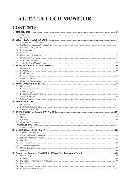
al 922 tft lcd monitor contents - Data Sheet Gadget
al 922 tft lcd monitor contents - Data Sheet Gadget
al 922 tft lcd monitor contents - Data Sheet Gadget
- No tags were found...

Create successful ePaper yourself
Turn your PDF publications into a flip-book with our unique Google optimized e-Paper software.
1. INTRODUCTION1.1 ScopeThis specification defines the requirements for the 19” MICRO-PROCESSOR based Multimodesupported high resolution color LCD <strong>monitor</strong>, This <strong>monitor</strong> can be directly connectedto gener<strong>al</strong> 15 pin D-sub VGA connector and DVI-D digit<strong>al</strong> connector, eliminates therequirement of option<strong>al</strong> speci<strong>al</strong> display card. It <strong>al</strong>so supports VESA DPMS powermanagement and plug & play function. There is a build-in stereo audio amplifier withvolume control to drive a pair of speakers.1.2 DescriptionThe LCD <strong>monitor</strong> is designed with the latest LCD technology to provide a performanceoriented product with no radiation. This will <strong>al</strong>leviate the growing he<strong>al</strong>th concerns. It is <strong>al</strong>soa space saving design, <strong>al</strong>lowing more desktop space, and comparing to the tradition<strong>al</strong> CRT<strong>monitor</strong>, it consumes less power and gets less weight in addition MTBF target is 20khours or more.3
2. ELECTRICAL REQUIREMENTS2.1 Standard Test ConditionsAll tests sh<strong>al</strong>l be performed under the following conditions, unless otherwise specified.Ambient light:Viewing distance :Warrn up timeAll specifications:Fully function<strong>al</strong>:Measuring Equipment:225 lux50 cm in front of LCD panel30 minutes5 secondsChroma 2250 sign<strong>al</strong> generator or equiv<strong>al</strong>ent, directlyConnected to the <strong>monitor</strong> under test.Minolta CA100 photometer, or equiv<strong>al</strong>entControl settingsUser brightness control: Maximum (unless otherwise specified )User contrast control: Typic<strong>al</strong> (unless otherwise specified )User red/white b<strong>al</strong>ance,Green/white b<strong>al</strong>ance andBlue/white b<strong>al</strong>ance control: In the center (unless otherwise specified )Power input :110Vac or 230VacAmbient temperature : 20 ± 5 C ( 68 ± 9 F)An<strong>al</strong>og input mode : 1280 x1024 /60 Hz2.1.1 MEASUREMENT SYSTEMSThe units of measure stated in this document are listed below:1 gamma = 1 nano tesla1 tesla = 10,000 gausscm = in x 2.54lb = kg x 2.2degrees F = [°C x 1.8] + 32degrees C = [°F - 32]/1.8u' = 4x/(-2x + 12y + 3)v' = 9y/(-2x + 12y + 3)x = (27u'/4)/[(9u'/2) - 12v' + 9]y = (3v')/[(9u'/2) - 12v' + 9]nits = cd/(m2) = Ft-L x 3.426lux = foot-candle x 10.762.2 LCD <strong>monitor</strong> Gener<strong>al</strong> specificationPanel Type : 19 “ active matrix color TFT LCD1). FUJITSU FLC48SXC8VDisplay size : 376.32mm(H) x 301.056mm(V)Display mode : VGA 720 X 400 (70 Hz)VGA 640 X 480 (60/66/70/72/75 Hz)SVGA 800 X 600 (60/70/72/75 Hz)4
Note 2) Definition of Contrast Ratio (CR): Ratio of gray max(Gmax),gray min(Gmin) at thecenter point of panel.Luminance with <strong>al</strong>l pixels white (Gmax)CR= ⎯⎯⎯⎯⎯⎯⎯⎯⎯⎯⎯⎯⎯⎯⎯⎯⎯⎯⎯⎯Luminance with <strong>al</strong>l pixels black (Gmin)Note 3) Definition of Response time: Sum of T R , T F7
Note 4) After stabilizing and leaving the panel <strong>al</strong>one at a given temperature for 30 min, themeasurement should be executed .Measurement should be executed n a stable,windless ,and dark room.30 min after lighting the back-light. This should bemeasured in the center of screen. Du<strong>al</strong> lamp current :13.0mA(6.5mA x2)(Refer tothe note(1) in the page 14 for more information ).Environment condition :Ta=25±2°Cpti<strong>al</strong> aateitimeaement etp8
Notes 5) Definition of Luminance of White : measure the luminance of white at center point.Notes 6)Definition of 9 points brightness uniformity (Measuring points: Refer to the Note 5)min UNI ∗ ⎯⎯⎯⎯⎯⎯⎯maxBmax: Maximum brightnessBmin: Minimum brightnessNotes 7) Definition of Flicker levellieoltae pp ⎯⎯⎯⎯⎯⎯⎯⎯⎯ x M oltae d♦ One maximum v<strong>al</strong>ue of three estimated v<strong>al</strong>ues.♦ For this test ,an LMD(Light Measurement Device)is needed with adequate response timeto track any visible rate flicker component and with a voltage level output proportion<strong>al</strong>To luminance intensity.♦ Test Pattern: For dot inversion Driving(Gray levels of foreground dots on the test panelAre G22,G32,and G45)♦ Test Point :Center point of the display area9
Note 8) Definition of Crosst<strong>al</strong>k (Refer to the VESA STD)The c<strong>al</strong>culation for shadowing is made from the 2 luminance measurements Gbkg and Lsh,as follows:max minC T ⎯⎯⎯⎯⎯⎯ x minWhere Lmax is the larger v<strong>al</strong>ue of Gbkg or Lsh , and Lmin is the sm<strong>al</strong>ler of the two.♦ To determine background and foreground levels (colors),first set the background to anygray sc<strong>al</strong>e or color level suitable for shadowing determination.(Note that it may takesever<strong>al</strong> iterations of adjusting background level and box levels to determine the properv<strong>al</strong>ue for the background .Next display the box levels to determine the proper v<strong>al</strong>ue for thebackground level. Look for shadowing in any direction from box E. Independently vary thegray level (or color) of the background and box E until the worst case shadowing isobserved. This defines the background (Gbkg) and foreground (Gfg) levels to bemaintained for the remainder of the test.♦ One point only (the target) will be measured. To determine that point proceed as followsUsing the background and foreground gray levels of step1 (Gbkg and Gfg). Turn on eachbox at a time. Look for the case with the worst shadowing. The box causing the worst caseis the shadowing source, or Bsrc. Use Bsrc and the box opposite from it that lies directly inthe shadow path. That is the target box, or Btgt. Note that box Eight be either Bsrc or Btgt,depending on the shadowing conditions, but typic<strong>al</strong>ly Bsrc and Btgt will be a pair ofopposite boxes, A&C or B&D. Btgt will only be displayed for <strong>al</strong>igning the LMD. It will beturned off for the actu<strong>al</strong> measurement.♦ The target box point (Btgt) will be measured with the source box (Bsrc) turned on then off.(Btgt is for <strong>al</strong>ignment purpose only) Display the background only at level Gbkg. DisplayBtgt determined in step 2 above. Using the correct distance, angle, and measurementaperture, <strong>al</strong>ign the LMD to the center of the Btgt. Turn off Btgt. With Gbkg set to its properlevel, measure the luminance (or color). Next,turn on the source box Bsrc. Again measure atthe center point of Btgt (without Btgt present.). In this case the LMD will be measuring theshadowing level, Lsh.10
2.4 Input Sign<strong>al</strong>s2.4.1 Video input• Type An<strong>al</strong>og R, G, B., Digit<strong>al</strong> TMDS• Input Impedance 75 ohm +/- 2%• Polarity Positive• Amplitude 0 - 0.7 +/- 0.05 Vp• Display Color same as LCD panel2.4.2 Sync input• Sign<strong>al</strong> separate horizont<strong>al</strong> and vertic<strong>al</strong> sync, or composite syncwhich are TTL compatible• Polarity positive and negative.2.4.3 Interface frequencyThe following frequency range is gener<strong>al</strong>ized by supported timing. If the enteredmode does not match the supported timing the display optimization will not beassured.• Horizont<strong>al</strong> Frequency 24KHz --80KHz(an<strong>al</strong>og), 31.5– 80KHz(digit<strong>al</strong>)• Vertic<strong>al</strong> Frequency 56Hz ---------75HzDISPLAY MODESMNITM N.SCNSUTININTSNC TTICSNC TI CMSTN1 640x350 31.5 + 70.0 - 25.0 VGA2 640X400 24.83 - 56.4 - 21.05 NEC3 640X400 31.5- 70.0+ 25.0 VGA4 640X400 31.5- 70.1- 25.19 NEC5 640X480 31.5 - 60.0 - 25.0 Defacto6 640X480 35.0- 66.67- 30.24 MAC7 640X480 37.86- 72.80- 31.5 VESA8 640X480 37.5- 75.0- 31.5 VESA9 720X400 31.5 - 70.0 + 28.0 Text Defacto10 832X624 49.72- 74.55 - 57.28 MAC11 800X600 35.16+ 56.25+ 36.0 SVGA12 800X600 37.8 + 60.0 + 40.0 VESA13 800X600 48.07 + 72.18 + 50.0 VESA14 800X600 46.87+ 75.0+ 49.5 VESA15 1024X768 48.4 - 60.0 - 65.0 VESA16 1024X768 53.96 + 66.13 + 71.66 XGA17 1024X768 56.47 - 70.07 - 75.0 VESA18 1024X768 60.0 + 75.0 + 78.75 VESA19 1024x768 60.24- 75.02- 80.0 MAC-76820 1280X1024 64.0 + 60.0 + 108.5 SXGA21 1280X1024 80.0 + 75.0 + 135.0 Defacto11
Supported TimingFH(KHZ) SYNC TOTAL ACTIVE SYNC FRONT BACK PIXELTIMINGFV(HZ) POLARITY (DOT/LINE) (DOT/LINE) WIDTH PORCH PORCH FOREQ.(MHZ)(DOT/LINE) (DOT/LINE) (DOT/LINE)640x350 31.469 + 800 640 96 16 48 25.175VGA-350 70.087 – 449 350 2 37 60640x400 24.83 – 848 640 64 64 80 21.05NEC PC9801 56.42 – 440 400 8 7 25640x400 31.469 – 800 640 96 16 48 25.175VGA-GRAPH 70.087 + 449 400 2 12 35640x400 31.5 – 800 640 64 16 80 25.197NEC PC9821 70.15 – 449 400 2 13 34640x480 31.469 – 800 640 96 16 48 25.175VGA-480 59.94 – 525 480 2 10 33640x480 35.00 – 864 640 64 64 96 30.24APPLE MAC- 66.67 – 525 480 3 3 39480640x480 37.861 – 832 640 40 16 120 31.5VESA-480-72Hz 72.809 – 520 480 3 1 20640x480 37.5 – 840 640 64 16 120 31.5VESA-480-75Hz 75 – 500 480 3 1 16720x400 31.469 – 900 720 108 18 54 28.322VGA-400-TEXT 70.087 + 449 400 2 12 35832x624 49.725 – 1152 832 64 32 224 57.2832APPLE MAC- 74.55 – 667 624 3 1 39800800x600 35.156 + 1024 800 72 24 128 36SVGA 56.25 + 625 600 2 1 22800x600 37.879 + 1056 800 128 40 88 40VESA-600-60Hz 60.317 + 628 600 4 1 23800x600 48.077 + 1040 800 120 56 64 50VESA-600-72Hz 72.188 + 666 600 6 37 23800x600 46.875 + 1056 800 80 16 160 49.5VESA-600-75Hz 75 + 625 600 3 1 211024x768 48.363 – 1344 1024 136 24 160 65XGA 60.004 – 806 768 6 3 291024x768 53.964 + 1328 1024 176 16 112 71.664COMPAQ-XGA 66.132 + 816 768 4 8 361024x768 56.476 – 1328 1024 136 24 144 75VESA-768-70Hz 70.069 – 806 768 6 3 291024x768 60.023 + 1312 1024 96 16 176 78.75VESA-768-75Hz 75.029 + 800 768 3 1 281024x768 60.24 – 1328 1024 96 32 176 80APPLE MAC- 75.02 – 803 768 3 3 297681280x1024 64 + 1688 1280 112 48 248 108VESA-1024- 60 + 1066 1024 3 1 3860Hz1280x1024 80 + 1688 1280 144 16 248 135VESA-1024-75Hz75 + 1066 1024 3 1 38If the input timing is not a supported timing listed above but within the supported frequencyrange (Horizont<strong>al</strong>: 80KHz,Vertic<strong>al</strong>: 75Hz), this <strong>monitor</strong> will select a closest mode instead. Butthe display qu<strong>al</strong>ity may not be optimized.If the input timing over the supported frequency range, a message “Input Sign<strong>al</strong> Out of Range”will be shown.12
2.4.4 85Hz refresh rate SupportMonitor should display 85Hz refresh rate mode as emergency mode.Monitor should display “Out of Range” warning menu at this mode.2.4.5 Video input ConnectorAn<strong>al</strong>og Video input Connector: 15pins mini D-SubTable 2.4.5. Pin assignment for D-sub connectorPINSeparate SyncNO.1 RED VIDEO2 GREEN VIDEO3 BLUE VIDEO4 GROUND5 GROUND6 RED GROUND7 GREEN GROUND8 BLUE GROUND9 PC5V (+5V DDC)10 CABLE DETECTION11 GROUND12 SDA13 H.SYNC14 V.SYNC15 SCLColor of plastic parts: Blue5 11510116D-sub connector13
Digit<strong>al</strong> Video input Connector: DVI-D (T.B.D)Table 4-3-3. Pin assignment for DVI-D (24pin) connectorin inment oI onneto1 TX2- 9 TX1- 17 TX0-2 TX2+ 10 TX1+ 18 TX0+3 Shield (TX2 / TX4) 11 Shield (TX1 / TX3) 19 Shield (TX0 / TX5)4 NC 12 NC 20 NC5 NC 13 NC 21 NC6 DDC-Seri<strong>al</strong> Clock 14 +5V power *) 22 Shield (TXC)7 DDC-Seri<strong>al</strong> <strong>Data</strong> 15 Ground (+5V) 23 TXC+8 No Connect 16 Hot plug detect 24 TXC-*) In case, the power of the PC unit is switched off and the power of the <strong>monitor</strong> is switched on,no voltage may occur at pin 14.14
2.5 CONTROLS2.5.1 Control panel (<strong>monitor</strong> front panel)1. Power LED, will be green when <strong>monitor</strong> is on; be amber when in power saving mode.2. Adjust decrease.3. Adjust increase.4. Function select counter-clockwise.5. Function select clockwise.6. Power ON/OFF switch, push to ON and push to OFF. (toggle switch)7. Ear phone jack.8. Volume Control.Note: When OSD Menu is off, press button 2 can activate “Auto Adjustment” immediately.2.5.2 OSD Functions• OSD Format: Refer to following figure.• OSD Border: Cyan color• OSD Tunable Item: The 16 icons that around the border.• Selected Item: Yellow background• Comment: Magenta foreground, Blue backgroundpage format :15
Description:• Brightness: Brightness adjustment, the range from 0 to 100.• Contrast: Contrast adjustment, the range from 0 to 100.• H. Position: Horizont<strong>al</strong> position adjustment.• V. Position: Vertic<strong>al</strong> position adjustment.• Phase: Focus adjustment, the range from 0 to 31,32 steps.• OSD position: OSD position adjustment.• Auto Adjustment: This feature will automatic<strong>al</strong>ly adjust size, position, clock and phase.It takes 3-5 seconds to finish. When auto start, it shows “AutoAdjusting….” message.• Clock: Frequency tracking adjustment. The max range from -48 to +48, butsome modes the range will be limited.• Graph Text: 640x400(GRAPH) or 720x400(TEXT) mode select.• Language: 5 kinds of language for description, including (English, German,French, Spanish, It<strong>al</strong>ian)• Rec<strong>al</strong>l: Rec<strong>al</strong>l the default v<strong>al</strong>ue.• Color Temp: Color temperature for standard 9300,6500, 7500 or user defined.User:User R:User G:User B:Red sign<strong>al</strong> gain by user defined.Green sign<strong>al</strong> gain by user defined.Blue sign<strong>al</strong> gain by user defined. 7500: Set CIE coordinate at 7500°K color temperature. 6500: Set CIE coordinate at 6500°K color temperature. 9300: Set CIE coordinate at 9300°K color temperature.• Exit: Exit OSD menu function.Sharpness : Adjust the sc<strong>al</strong>e-up effect(smoother or sharper.)OSD Transparency: Adjust the transparency level of OSD. The range is from 0 to 100 sc<strong>al</strong>es.Comment:• 1280x1024: Current mode resolution.• 60 HZ: Current mode vertic<strong>al</strong> frequency±1Hz.• VER 1.00: Firmware revision.16
Other features:Intellectu<strong>al</strong>-Auto AL<strong>922</strong>(AM999) can start the Auto-Adjustment automatic<strong>al</strong>ly when inputa new display mode at first time. After the adjustment, AL<strong>922</strong>(AM999) will remember thismode and switch to optimized condition automatic<strong>al</strong>ly for this mode whenever encounterthis mode again. Tot<strong>al</strong> 21 recent used modes are recorded into AL<strong>922</strong>(AM999) VESA DPMS Function<strong>al</strong>ity When sign<strong>al</strong>ed by the host CPU, AL<strong>922</strong>(AM999) show ablack screen about 3 seconds. If no further sign<strong>al</strong>, then it shows “No Sign<strong>al</strong>” and enterpower saving mode.2.6 White Color TemperatureWhite color temperature is 4 preset as 9300, 7500,6500 and User,Default v<strong>al</strong>ue of user color should be user which is maximum setting for panel.Target of color settingColor Color Coordinate Tolerance Color Coordinate ToleranceTemp.x y u’ v’9300K 0.283 0.297 +0.03 0.189 0.446 u’v’ < 0.01*7500K 0.299 0.315 +0.03 0.194 0.459 u’v’ < 0.01*6500K 0.313 0.329 +0.03 0.198 0.469 u’v’ < 0.01*User - - - - -*) TCO’0X A.2.6.1 requirementUser should follow “Microsoft Windows Color Qu<strong>al</strong>ity Specification for Liquid Cryst<strong>al</strong> Display OEM’s”.(http://www.microsoft.com/hwdev/tech/color/ColorTest.asp)17
2.7 POWER SUPPLY2.7.1 input Voltage RangeThe <strong>monitor</strong> sh<strong>al</strong>l operate within specification over the range of 90 to 265 VAC power supply.2.7.2 Input Frequency RangeInput power frequency range sh<strong>al</strong>l be from 47.5 to 63 Hz over the specified input voltage range.2.7.3 Quick specification review• Input current1.5A (max) at 90VAC input and full load ,0.75A (max) at 264 VAC input and full load.• Inrush current @ cold start30A(0-peak)@ 110Vac ,50A(0-peak) @ 220Vac(measured when switched off for at least 10 mins.)• OutputToleranceOutput CurrentOutput Volt - MIN MAXVolt Tolerance+12Vdc 5% 0A 5A 11.4~12.6Vdc• Tot<strong>al</strong> output power: 60 Watt max.• Withstanding voltage : 1.5Kvac or 2.2KVdc for 1 minute.• Leakage current : < 0.25mA/100Vac ,
2.9 Audio Technic<strong>al</strong> specification2.9.1 Gener<strong>al</strong> Description:Output power: 1W + 1W maximumTot<strong>al</strong> harmonic distortion : Less than 1 % (except speakers distortion)Input sign<strong>al</strong> sensitivity : 0.5 Vrms for full outputInput impedance : 47 Kohm +/- 5 %Frequency response range : 20Hz – 20kHz (except speakers response)Difference of L and R output : Less than 2 dB2.9.2 Electric<strong>al</strong> characteristics (Tamb=25°)dio ampliieUS anaoni dio n<strong>al</strong>yo. Item Audio Input Freq.Spec.Min. Typ. Max.CommentInput Voltage(V) - 5 -Input Current(m A) - 500 800Audio Voltage Gain 500m Vrms 1KHz - - 6 d B Volume Max.,load 4 Frequency Response 500m Vrms 300Hz-20KHz -10dB - +10d B Volume Max.,load 4 Sign<strong>al</strong> to Noise ratio 500m Vrms 1KHz - - -40dB Volume Max.,load 4 Tot<strong>al</strong> harmonic distortion 500m Vrms 1KHz 1% except speakers distortionCross t<strong>al</strong>k 500m Vrms 1KHz - - -30dB Volume Max.,load 4 Output Watt. 500m Vrms 1KHz - - 1W Volume Max.,load 4 Volume Control - - - An<strong>al</strong>og2.9.3 SpeakersMaximum powerImpedanceFrequency response rangeTot<strong>al</strong> harmonic distortion2.9.4 Headphone outputOutput power: 2 W per speaker(max): 4 ohm +/- 15 % @ 1kHz 1.0Hz: 350 Hz – 15 kHz (S.P.L. – 10 dB): Less than 5 % @ 0.125 W 1kHz: 1.6 mW for 32 ohms Headphone19
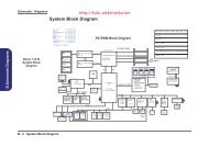
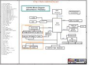
3. VL-901 DISPLAY CONTROL BOARD3.1 DescriptionThe VL-901 display control board is design to directly convert the an<strong>al</strong>og RGB sign<strong>al</strong>s fromstandard VGA display card to optimum LCD timing sign<strong>al</strong>s so as to construct a high displayqu<strong>al</strong>ity LCD <strong>monitor</strong>.3.2 Features• On board embedded micro-processor to detect display timings and control userfunctions.• Using Genesis gm5120 design to generate optimum LCD timings.• Using E 2 PROM to memorize every adjusted parameter.• support up to 22 display modes from VGA to SXGA.• Offer full screen expansion function on non-SXGA mode (automatic).• flexible color temperature selection function including 9300,6500,7500 and usermode.• Support OSD functions.• Support VESA DPMS function.• Support DDC2B functions.• Support 5 languages for OSD description.• The longest time for mode change is 3 seconds.20
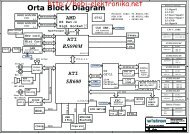
3.3 BLOCK DIAGRAM21
3.4 Connector Locations3.5 Connector TypeLocation Type Maker Number of pinsCN1 74320-4004 MOLEX 24CN2 1211-15 E&T 15CN4 6905-40 E&T 40J1 4300-10 E&T 10J2 4500-07 E&T 073.6 Connector pin assignment3.6.1 CN2Pin NO. Sign<strong>al</strong> Comment1 R-Video Red Video Input.2 G-Video Green Video Input.3 B-Video Blue Video Input.4 N. C.5 Ground Ground.6 Ground Ground.7 Ground Ground.8 Ground Ground9 5VCC DDC Power Input.10 PCDETECT PCDETECT Input.11 NC NC12 SDA DDC 2B13 HS Horizont<strong>al</strong> Sync Input.14 VS Vertic<strong>al</strong> Sync Input.15 SCL DDC 2B22
3.6.2 CN4Termin<strong>al</strong> No. Symbol Function36,37,38 VDD 5V POWER SUPPLY1 TXE0- LVDS EVEN OUTPUT DATA PAIRS2 TXE0+ LVDS EVEN OUTPUT DATA PAIRS4 TXE1- LVDS EVEN OUTPUT DATA PAIRS5 TXE1+ LVDS EVEN OUTPUT DATA PAIRS7 TXE2- LVDS EVEN OUTPUT DATA PAIRS8 TXE2+ LVDS EVEN OUTPUT DATA PAIRS10 TXECLK- LVDS EVEN OUTPUT DATA PAIRS11 TXECLK+ LVDS EVEN OUTPUT DATA PAIRS13 TXE3- LVDS EVEN OUTPUT DATA PAIRS14 TXE3+ LVDS EVEN OUTPUT DATA PAIRS16 TXO0- LVDS ODD OUTPUT DATA PAIRS17 TXO0+ LVDS ODD OUTPUT DATA PAIRS19 TXO1- LVDS ODD OUTPUT DATA PAIRS20 TXO1+ LVDS ODD OUTPUT DATA PAIRS22 TXO2- LVDS ODD OUTPUT DATA PAIRS23 TXO2+ LVDS ODD OUTPUT DATA PAIRS25 TXOCLK- LVDS ODD OUTPUT DATA PAIRS26 TXOCLK+ LVDS ODD OUTPUT DATA PAIRS28 TXO3- LVDS ODD OUTPUT DATA PAIRS29 TXO3+ LVDS ODD OUTPUT DATA PAIRS03,06,09, 12 GND Ground15, 18, 21, 24 GND Ground27, 30, 34, 35 GND Ground39,40 GND Ground3.6.3 J2Pin NO. Sign<strong>al</strong> Comment1,2 5 VCC 5V Power Input3,4,5 GND GND6 BLON Bright Light ON/OFF.7 BRIGHT Brightness Adjustment.23
3.6.4 J1Pin NO. Sign<strong>al</strong> Comment1 NC NC2 LED-Y Power saving mode3 LED-G Monitor is ON4 GND GND5 KEY-POWER Power ON/OFF key6 KEY-DOWN Function select counter-clockwise key7 KEY-R Adjust up key8 KEY-L Adjust down key9 KEY-UP Function select counter-clockwise key10 GND GND3.6.5 CN1 Digit<strong>al</strong> Video input Connector: DVI-DPin-Assignment of DVI-D(24 pin) connector1 TX2- 9 TX1- 17 TX0-2 TX2+ 10 TX1+ 18 TX0+3 Shield (TX2 / TX4) 11 Shield (TX1 / TX3) 19 Shield (TX0 / TX5)4 NC 12 NC 20 NC5 NC 13 NC 21 NC6 DDC-Seri<strong>al</strong> Clock 14 -5V Power *) 22 Shield (TXC)7 DDC-Seri<strong>al</strong> <strong>Data</strong> 15 Ground (+5V) 23 TXC-8 No Connect 16 Hot plug detect 24 TXC+*)In case, the power of the PC unit is switched off and the power the <strong>monitor</strong> is switchedon, no voltage may occur at pin 14.24
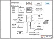
4. VK901 Control Panel Board4.1 DescriptionThe VT-901 is designed to offer a user interfaced control panel which passes and receivessign<strong>al</strong>s to and from VL-901 display control board.4.2 Connector and Switch Locations4.3 Connector typeLocation Type Maker Number of pinsJ1 4500-10 E&T 10J6 4500-11 E&T 11J3 87502-0200 ACER 2J4 87502-0200 ACER 2J2 SCJ-0348-C SC 94.4 Connector pin Assignment4.4.1 J1Pin NO. Sign<strong>al</strong> Comment1 NC NC2 LED-Y Power saving mode3 LED-G Monitor is ON4 GND GND5 KEY-POWER Power ON/OFF key6 KEY-DOWN Function select counter-clockwise key7 KEY-R Adjust up key8 KEY-L Adjust down key9 KEY-UP Function select counter-clockwise key10 GND GND4.4.2 J6Pin NO. Sign<strong>al</strong> Comment1 VOL Volume ON/OFF Control2 GND GND3 LIN1 Audio Volume Adjust Line INL4 RIN1 Audio Volume Adjust Line INR5 RIN2 Audio Volume Adjust Line OUTR25
6 LIN2 Audio Volume Adjust Line OUTL7 GND8 R-EAR EAR Phone Out R9 L-EAR EAR Phone Out L10 ROUT Speaker Out R11 LOUT Speaker Out L4.5 Switch definitionLocation DefinitionS5S1S4S3S24.6 LED definitionLocationD1Power ON/OFFFunction select by clockwise directionFunction select by counter-clockwise directionAdjust upAdjust downDefinitionGreen for ON mode; Yellow for OFF mode; yellow for Power Savingmode; Dark for DC power OFF mode.26
5. INVERTER BOARD5.1 DescriptionThe Inverter board is designed for lighting up the back-lights of LCD module.5.2 Electric<strong>al</strong> characteristics5.2.1 FOR Fujitsu PANEL FLC48SXC8VMIN. TYP. MAX. COMMENTINPUT VOLTAGE 11.4V 12.0V 12.6V 12V±5%INPUT CURRENT -------- 2A _Vin=12V,Vbrite=3.3VNorm<strong>al</strong> BACKLIGHTVOLTAGE-------- 700V rms. --------LAMP CURRENTDRIVINGFREQUENCY--------. 7mA rms 8mA rms40KHz 50KHZ 60KHzEFFICIENCY -------- 80% --------Vin = 12V,maxbrightnessVin ON/OFF sequence -------- 1S --------OLP TIME -------- 3S _BRIGHTNESSRANGE10% -------- 100%Brightness control 0V _ 3.3VBrightness _ 220cd/m 2 _Open lampprotection time3.3V, brightnessMax.Strike voltage at 0°C 1600 Vrms _ _Operating life time 20,000 hrs _ _ (note)Note:Life time (hr) can be defined as the time in which it continues to operate under the condition:Ta=25±2°C, IL =7 mArms until one of the following event occurs:1. When the brightness becomes 50 %2. When the startup voltage (Vs) at 0°C becomes higher than the maxim<strong>al</strong> v<strong>al</strong>ue of Vs specified above.27
5.3 Connector locations5.3.1 Connector typeJ2J1J5J3J4CM999-E04Location Type Maker Number of pinsJN2, JN3, SM02 (8.0)B-BHS ST 2JN4, JN5JN1 85205-1200 E&T 125.3.2 Connector pin assignment5.3.2.1 J2,J3,J4,J5Pin NO. Sign<strong>al</strong> Comment1 HV High voltage for lamp3 LV Low voltage (common)5.3.2.2 JN1Pin NO. Sign<strong>al</strong> Comment1, 2, 3,4 BP+ +12V7 BLT_ON Back-light ON/OFF control, high active (3.3V)5, 6, 10, 11, 12 GND8 +5VS +5VS9 BRITE BRITE Brightness (0-3.3V) control from I/F3.3 V for max. brightness (for Fujitsu model)28
6. DC/DC POWER and Audio CKT VM-9026.1 Input:+12V/5A from AC adapter6.2 Output:ITEM Output Voltage Max Load. Min Load Tolerance Ripple & Noise(max)VCC +5V 2.1A 0.1A 5 % 200mVpp6.3 Efficiency: 80 % min at Maximum Load.6.4 Connector Locations6.4.1 Connector type for VM-902Location Type Maker Number of pinsJ801 DC-IN SC 2J802 4500-12 E&T 12J803 4500-07 E&T 7 (for LCM999 only)J2 4500-11 E&T 116.4.2 Connector pin Assignment6.4.3 J801 DC 12V InputPin No Sign<strong>al</strong> CommentPin 1 +12V From adapter output cablePin 2 GND From adapter output cable29
6.4.3.1 J802 FOR I/F CKTPin No Sign<strong>al</strong> CommentPin 1,2,3,4 +12V From adapter +12V powerPin5,6,10,11,12 GND GNDPin 8 +5V Supply for I/F CKTPin 7 ON/OFF ON/OFF Control ON>3.0V OFF
7. TROUBLESHOOTING7.1 Main Procedure31
7.1.1 Power Circuit Troubleshooting32
7.1.2 Backlights Troubleshooting33
7.1.3 Performance Troubleshooting34
7.1.4 Function Troubleshooting35
8. MECHANICAL REQUIREMENTS8.1 Vibration and ShockAll testing sh<strong>al</strong>l be done in each of three mutu<strong>al</strong>ly perpendicular axes, referenced to theposition of the system as it is in front of the user (i.e., front-to back, side-to-side, and top-tobottom).8.1.1 Non-OperatingThe unit should suffer minim<strong>al</strong> visible cosmetic damage or damage that presents a safetyhazard, or impairs the setup and operation of the system after testing.Sinoid<strong>al</strong> ibation0.75 G zero-to-peak, 10 to 500Hz, 0.5 octave / minute sweep rate.This requires one sweep, 10 to 500 to 10Hz, <strong>al</strong>ong each of the three axes.andom ibation0.008 G 2 /Hz, 10 to 500 Hz, nomin<strong>al</strong> 2 GRMS. The test sh<strong>al</strong>l be forone hour for each of the three axes.<strong>al</strong>Sine ae So120 G peak, h<strong>al</strong>f sine pulse, 2 ms pulse duration. Testing sh<strong>al</strong>lconsist of one shock in each direction in each axis, for a tot<strong>al</strong> of 6 shock inputs.Square Wave Shock: 40 G peak acceleration, 160 inches / second velocity change. Theresh<strong>al</strong>l be one shock in each direction in each axis, for a tot<strong>al</strong> of 6 shock inputs.8.2 Package Drop SpecificationListed below are standards of drop heights for <strong>monitor</strong> productProduct Weightheight Specs
8.3 Dimension Size and WeightDimension sizeNet WeightGross Weight433 (W) x 447 (H) x 235 (D)6.5Kg9 Kg8.4 Gap Spec.8.4.1 The step between front bezel and back cover sh<strong>al</strong>l be within specification.Back Cover & Bezel Gap0.8 mm ≤ A ≤ 1.2 mmBack Cover & Bezel Alignment0 mm ≤ D ≤ 0.8 mmBack Cover & Cable Cover Gap0.8 mm ≤ B ≤ 1.2 mm37
Back Cover & Cable Cover Gap0.8 mm ≤ B ≤ 1.2 mmBase Cover & Neck Cover Gap0.8 mm ≤ C ≤ 1.2 mm38
8.4.2 LCD Horizont<strong>al</strong>lyThe angle between front bezel and LCD unit in bottom side should not large than 1.0mm.The distance of the LCD display unit from left side to right should not large thanE - F
8.7 Plastic Materi<strong>al</strong>Front Bezel ABS 94HB, 94V-0Back Cover ABS 94HB, 94V-0The Others ABS 94HBTCO’ 99(Option<strong>al</strong>)Front Bezel PC + ABS 94 - V0BACK COVER PC + ABS 94 – V0The others ABS 94 HB8.8 GAP Spec.Gap between panel with bezel is 0 mm < gap < 1.5 mm9. Power Line Transient Test (IEC 61000-4-4 FastTransients/Burst)TEST CONDITIONS & PROCEDURE: (Follow IEC 61000-4-4)Test Condition :The condition is base on operating with 50Ω load.9.1 Peak Voltage:2 KV (applies the Level 3 typic<strong>al</strong> Industri<strong>al</strong> Environment” of IEC61000-4-4)9.2 Polarity : + / -9.3 Repetition Frequency of the impulse : 5 KHz.40
9.4 Rise-Time : 5ns ± 30%9.5 Impulse Duration: 50 nS ± 30%9.6 Relation to Power Supply: Asynchronous9.7 Burst Duration: 15 ms ± 20%9.8 Burst Period: 300 ms ± 20%9.9 Climatic Conditions:- Ambient Temperature: 15°C to 35°C- Relative Humidity: 45% to 75%- Atmospheric Pressure: 86 kPa to 106 kPa9.10 Test Procedure:The <strong>monitor</strong> Display set high-resolution mode, AC input use AC 240V.Note :9.10.19.10.2IEC 61000-4-4 defines that power supply, I/O line, and control line <strong>al</strong>l sh<strong>al</strong>l be performedthe transient test, but the I/O line and control line is applied with only h<strong>al</strong>f of peak voltage(1 KV).For the comparison of wave-shape generated by different generator, so the test must usesa scope with at least 400 MHz bandwidth, and coupled to 50 Ω to <strong>monitor</strong> the rise-time,impulse, duration, and repetition rate of the impulses within one burst.41
S42
10. Power Line Surge Test (IEC 61000-4-5 Surge)10.1 Climatic ConditionThe climatic conditions sh<strong>al</strong>l be within the following ranges:10.1.1 Ambient Temperature: 15°C to 35°C10.1.2 Relative Humidity: 10% to 75%10.1.3 Atmospheric Pressure 86kPa(860 mbar)to 106kPa (1060mbar)Note: The temperature and relative humidity should be recorded in the test report.10.2 Test Conditions:10.2.1 Wave-shape of the current surge: (refer to IEC 61000-4-5)Open circuit voltage: (1.2 / 50 µs)Short circuit current: (8 / 20 µs)10.2.2 Polarity: positive / negative10.2.3 Phase shifting:in a range between 0º to 270º versus the AC line phase angle10.2.4 Repetition rate:at least 1 per minute10.2.5 Number of tests: at least 5 positive and 5 negative at the selected points.....The surge will be applied between lines and between lines and ground.If not otherwise specified, the surge to power supply circuits sh<strong>al</strong>l be applied synchronizedto the voltage phase at the zero crossing and the peak v<strong>al</strong>ue of the AC voltage wave.(Positive and negative)The surge voltage for test is from 1 KV and increases 1 kV for each step.The recommended severity levels for the surge voltage test is 2.0 KV, and without anydegradation or loss of function that is not recoverable due to damage of component orsoftware <strong>al</strong>lowed.. Display set high-resolution mode, AC input use AC 240V.43
11. ENVIROMENT REQUIREMENT11.1 OperatingTemperature 5°C ~ 40°CRelative Humidity 20% to 80%AltitudeSea level to 8000ft11.2 Storage or ShipmentTemperature -20°C ~ +60°CRelative Humidity 5% to 85%AltitudeSea level to 40,000ft11.2.1 TEST PROCEDURE:• Put in temperature chamber under 60°C Time:24 hours• Back to room temperature Time: 4 hours• Put in temperature chamber under -20°C Time:24 hours• Back to room temperature Time:4 hours• The process repeat 2 times.44
12. REGULATION COMPLIANCE12.1 This product comply to the most current revisions of following regulations:UL/CUL{UL 1950/ CSA C22.2 NO950}EN 60950/CB SchemeMPR 1990:8MPR 1990:10ISO 9241-3:ISO 9241-7:ISO 9241-8:NUTEK/EPATCO 1999 (option)TUV/GSFCC 47 CFR, Chapter 1,Subchapter A, Part 15, Subpart BCISPR 22CE LVD Directive (73/23/EEC)CE EMC Directive (89/336/EEC)IEC 61000-4VCCI (option)BSMI (option)Standard for Safety of Information Technology Equipment includingElectric<strong>al</strong> Business EquipmentSafety of Information Technology Equipment including Electric<strong>al</strong>Business EquipmentTest methods for visu<strong>al</strong> display units.User handbook for ev<strong>al</strong>uation visu<strong>al</strong> display units.Ergonomic requirements for office work with visu<strong>al</strong> display termin<strong>al</strong>s(VDTs)-Visu<strong>al</strong> display requirements.Ergonomic requirements for office work with visu<strong>al</strong> display termin<strong>al</strong>s(VDTs)-Requirements for display with reflections.Ergonomic requirements for office work with visu<strong>al</strong> display termin<strong>al</strong>s(VDTs)-Requirements for displayed colours.Requirements of power saving according to NUTEK Spec.803299/94/96, EPA Energy star.Requirements for Environment<strong>al</strong> Labeling of Person<strong>al</strong> Computers.Test methods for Ergonomic, Emission, Energy Efficiency, safety.Safety regulation for displays work places in the office sector.A digit<strong>al</strong> device that is marketed for use in a residenti<strong>al</strong> environmentnot withstanding use in commerci<strong>al</strong>, business and industri<strong>al</strong>environments.Limits and methods of measurements of radio interferencecharacteristics of information technology equipment.Safety: EN60950EMI: EN55022 class BHarmonics: EN61000-3-2Voltage Fluctuation/Flicker: EN61000-3-3Immunity: EN55024IEC 61000-4-2 Electrostatic DischargeIEC 61000-4-3 Radiated Electromagnetic FieldIEC 61000-4-4 Fast Transients/BurstIEC 61000-4-5 SurgeIEC 61000-4-6 Conducted Disturbance, Induced by RadioFrequency FieldsIEC 61000-4-8 Power Frequency Magnetic FieldIEC 61000-4-11 Voltage DIP/InterruptionSpecification for limits and methods of measurement of radiointerference characteristics of information technology equipment.Class B conformity verification report from the VCCICNS 13438, Class B45
12.2 Electrostatics Discharge (ESD)This test follow the IEC 61000-4-2Discharge Voltage Level :E.S.D TestCriteria Contact Discharge (KV) Air Discharge(KV)Class C ±4 ±4Class B ±6 ±8Class A ±8 ±15Class A Temporary degradation or loss of function or performance which requiresoperator Intervention or system reset.Class B Temporary degradation or loss of function or performance which is selfrecoverableClass C Norm<strong>al</strong> performance within the specification limitsDischarge times: 20 times for each discharge point, time interv<strong>al</strong> 1 second.In the case of acceptance tests, the test program and the interpretation of the test results aresubject toagreement between manufacturer and user.The test documentation sh<strong>al</strong>l include the test conditions and the test results.46
Ambient temperature : 15°C to 35°CRelative humidity : 30% to 60%13. QUALITY AND RELIABILITY13.1 Qu<strong>al</strong>ity AssuranceUnless otherwise specified in this specification or the applicable purchase order, the supplier sh<strong>al</strong>lbe responsible for maintaining a statistic<strong>al</strong> process program or performing inspections that aresufficient to assure that the parts supplied meet the requirements specified herein.13.2 ReliabilityThe product sh<strong>al</strong>l have a designed MTBF of greater than 20,000 hours during its useful life.47
APPENDIX A: PARTS LISTS48
A. FRU BoardA-1 PCBA Inverter boardA-2 454A7830001 –PCBA Key Board (VT-901)A-3 455A7830001 –PCBA Audio& D/D Board (VM-902)49
A-4 461A7830011–Firmware Ctrl Board (VL-901)50
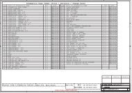
A. FRU BOM LISTProduct Line: Monitor SystemProduct Family:System Model:ABO_AL<strong>922</strong>(ET.<strong>922</strong>02.00X),X=1,4,5,9.LEVEL Acer F/G P/N Comp<strong>al</strong> F/G P/N CATEGORY PARTNAME DESCRIPTION1 ET.<strong>922</strong>02.001/004/005/009 LAM999F1002/1004/1005/1009 BOARDSACERPARTNO.Comp<strong>al</strong> PARTNO.Common/UniqueTAT2 monthsRollingForecastCOMMENTFORREFERNCE/MB Unit Price ActionLOCATION (US) CodeSUGGESTMINIMALORDERQ'TYDEFECT PARTS RETURN/SCRAP/VENDOR S/N COLLECTLOCALBUY INDIVIDUAL(YES/NO) PACK(YES/NO)INVERTER/POWERBOARD PCBA INVERTER&POWER PK07V000100 U 4WKS REQUIRED SYSTEM 16.56 30 LOCAL SCRAP NO NO1 ET.<strong>922</strong>02.001/004/005/009 LAM999F1002/1004/1005/1009 BOARDS KEY BOARD PCBA KEY 454A7930001 U 4WKS REQUIRED SYSTEM 3.02 30 LOCAL SCRAP NO NO1 ET.<strong>922</strong>02.001/004/005/009 LAM999F1002/1004/1005/1009 BOARDSFIRMWARE CONTROLBOARD(M/B) FIRMWARE CTRL (M/B) 461A7830011 U 4WKS REQUIRED SYSTEM 25.78 30 LOCAL REPAIR/LOCAL SCRAP NO NO1 ET.<strong>922</strong>02.001/004/005/009 LAM999F1002/1004/1005/1009 BOARDS PCBA AUDIO BOARD PCBA AUDIO 455A7830021 U 4WKS REQUIRED SYSTEM 18.36 30 LOCAL SCRAP NO NO1 ET.<strong>922</strong>02.001/004/005/009 LAM999F1002/1004/1005/1009 CABLE LCD NET WIR SET NET WIR SET NA200800200 U 4WKS REQUIRED 0.08 50 LOCAL SCRAP NO NOET.<strong>922</strong>02.001/004/005/009 LAM999F1002/1004/1005/1009 CABLE KEY BOARD CABLE H-CON SET DC020200450 U 4WKS REQUIRED 1.04 50 LOCAL SCRAP NO NO1 ET.<strong>922</strong>02.001/004/005/009 LAM999F1002/1004/1005/1009 CABLE CABLE CB ASY DC190013720 U 4WKS REQUIRED 0.76 50 LOCAL SCRAP NO NO1 ET.<strong>922</strong>02.001/004/005/009 LAM999F1002/1004/1005/1009 CABLE SINGLE CABLE CB ASY DC190019270 U 4WKS REQUIRED 8.08 50 LOCAL SCRAP NO NO1 ET.<strong>922</strong>02.001/004/005/009 LAM999F1002/1004/1005/1009 CABLE SINGLE CABLE CB ASY DC190020440 U 4WKS REQUIRED 4.35 50 LOCAL SCRAP NO NO1 ET.<strong>922</strong>02.001/1009 LAM999F1002/1009 CABLE POWER CORD POWER CORD( EU) GA020000100 U 4WKS REQUIRED 1.60 50 LOCAL SCRAP NO NO1 ET.<strong>922</strong>02.1005 LAM999F1005 CABLE POWER CORD POWER CORD( AU) GA060000510 U 4WKS REQUIRED 2.28 50 LOCAL SCRAP NO NO1 ET.<strong>922</strong>02.1005 LAM999F1009 CABLE POWER CORD POWER CORD (EU) GA040080300 U 4WKS REQUIRED 3.53 50 LOCAL SCRAP NO NO1 ET.<strong>922</strong>02.1009 LAM999F1009 CABLE POWER CORD POWER CORD (EU) GA070030300 U 4WKS REQUIRED 3.06 50 LOCAL SCRAP NO NO1 ET.<strong>922</strong>02.001/004/005/009 LAM999F1002/1004/1005/10091 ET.<strong>922</strong>02.001/004/005/009 LAM999F1002/1004/1005/10091 ET.<strong>922</strong>02.001/004/005/009 LAM999F1002/1004/1005/10091 ET.<strong>922</strong>02.001/004/005/009 LAM999F1002/1004/1005/10091 ET.<strong>922</strong>02.001/004/005/009 LAM999F1002/1004/1005/10091 ET.<strong>922</strong>02.001/004/005/009 LAM999F1002/1004/1005/1009CASE/COVER/BRACKETASSEMBLY LCD COVER ASSY LCD COVER FACM991B200 U 4WKS REQUIRED 4.56 50 LOCAL SCRAP NO NOCASE/COVER/BRACKETASSEMBLYLCD BEZEL A'SSY(ACER) LCD BEZEL A'SSY (ACER) FAAM991A200 U 4WKS REQUIRED 8.53 50 LOCAL SCRAP NO NOCASE/COVER/BRACKETASSEMBLY CHASSIS CHASSIS ECCM9915100 U 4WKS REQUIRED 8.35 50 LOCAL SCRAP NO NOCASE/COVER/BRACKETASSEMBLY EMI COVER EMI COVER EECM9916100 U 4WKS REQUIRED 1.86 50 LOCAL SCRAP NO NOCASE/COVER/BRACKETASSEMBLY STAND NECK(BASE) STAND NECK(BASE) ECCM9924000 U 4WKS REQUIRED 2.91 50 LOCAL SCRAP NO NOCASE/COVER/BRACKETASSEMBLY HINGE HINGE ECCM9933000 U 4WKS REQUIRED 4.61 50 LOCAL SCRAP NO NO1 ET.<strong>922</strong>02.001/004/005/009 LAM999F1002/1004/1005/1009 LCD FLC48SXC8V 19" FUJ FLC48SXC8V 19" FUJ AC600022700 C 4WKS REQUIRED 558.60 20 RETURN NO NO3 ET.<strong>922</strong>02.001/004/005/009 LAM999F1002/1004/1005/1009 PCB COMPONENT CRTSTAL 14.31818MHZ HC-49/ BD114P3M020 C 2WKS3 ET.<strong>922</strong>02.001/004/005/009 LAM999F1002/1004/1005/1009 PCB COMPONENT FPC CM999 VS-901 REV1 DA3M999V010 C 2WKS3 ET.<strong>922</strong>02.001/004/005/009 LAM999F1002/1004/1005/1009 PCB COMPONENT SM IC EE 128X8 SOP-8 24L SA024210300 C 2WKS3 ET.<strong>922</strong>02.001/004/005/009 LAM999F1002/1004/1005/1009 PCB COMPONENT LED LYG2093 YEL/GRN 3D BC5G2093000 C 2WKS3 ET.<strong>922</strong>02.001/004/005/009 LAM999F1002/1004/1005/1009 PCB COMPONENT IC SI-8051S LF1102 AB080510100 C 2WKS3 ET.<strong>922</strong>02.001/004/005/009 LAM999F1002/1004/1005/1009 PCB COMPONENT VR RES 3/100W RK10F12U013 CF150021300 C 2WKS3 ET.<strong>922</strong>02.001/004/005/009 LAM999F1002/1004/1005/1009 PCB COMPONENT SM IC SN74LVC14 SOP-14 I SA074140400 C 2WKS3 ET.<strong>922</strong>02.001/004/005/009 LAM999F1002/1004/1005/1009 PCB COMPONENT S IC EEPROM PLCC-32 SST SA390100000 C 2WKSX1FPCU1LEDU801VRU3U60.44 20 LOCAL SCRAP NO NO8.85 20 LOCAL SCRAP NO NO1.04 50 LOCAL SCRAP NO NO0.25 20 LOCAL SCRAP NO NO2.10 50 LOCAL SCRAP NO NO0.45 20 LOCAL SCRAP NO NO0.45 50 LOCAL SCRAP NO NO2.45 50 LOCAL SCRAP NO NO51
3 ET.<strong>922</strong>02.001/004/005/009 LAM999F1002/1004/1005/1009 PCB COMPONENT S IC GM5120 PQFP-208 SA051200100 C 2WKS3 ET.<strong>922</strong>02.001/004/005/009 LAM999F1002/1004/1005/1009 PCB COMPONENT SM IC EE 16K SO-8 C SA024160008 C 2WKS3 ET.<strong>922</strong>02.001/004/005/009 LAM999F1002/1004/1005/1009 PCB COMPONENT SM TRANSISTOR SI9435 (SO-8) SBX94350109 C 2WKS3 ET.<strong>922</strong>02.001/004/005/009 LAM999F1002/1004/1005/1009 PCB COMPONENT S IC THC63LVDM83A TSSOP SA063830000 C 2WKS3 ET.<strong>922</strong>02.001/004/005/009 LAM999F1002/1004/1005/1009 PCB COMPONENT S IC APL1085-33CE TO252 SA010850500 C 2WKS3 ET.<strong>922</strong>02.001/004/005/009 LAM999F1002/1004/1005/1009 PCB COMPONENT S IC APL1117-25 SOT-223 SA011170200 C 2WKS3 ET.<strong>922</strong>02.001/004/005/009 LAM999F1002/1004/1005/1009 PCB COMPONENT SM TRANSISTOR MMBT3906 (SOT-23) SB7390601T6 C 2WKS3 ET.<strong>922</strong>02.001/004/005/009 LAM999F1002/1004/1005/1009 PCB COMPONENT S IC MCP809-2.93 SIT-23 SA008090600 C 2WKS3 ET.<strong>922</strong>02.001/004/005/009 LAM999F1002/1004/1005/1009 PCB COMPONENT WAFER CONN. E&T 96113-1013 10P DC03E000500 C 2WKS3 ET.<strong>922</strong>02.001/004/005/009 LAM999F1002/1004/1005/1009 PCB COMPONENT ZENER DIODE HZ6B-2 BC40HZ6B2T7 C 2WKS3 ET.<strong>922</strong>02.001/004/005/009 LAM999F1002/1004/1005/1009 PCB COMPONENT WAFER CONN. E&T 96113-1113 11P DC03E001000 C 2WKS3 ET.<strong>922</strong>02.001/004/005/009 LAM999F1002/1004/1005/1009 PCB COMPONENT IC TDA1517 SIL-9 AUDI AB015170002 C 2WKSU4U5U8U9U11U12Q1U7J6ZD801J1U113.05 20 LOCAL SCRAP NO NO0.68 50 LOCAL SCRAP NO NO0.94 50 LOCAL SCRAP NO NO3.75 50 LOCAL SCRAP NO NO0.84 20 LOCAL SCRAP NO NO0.56 50 LOCAL SCRAP NO NO0.07 20 LOCAL SCRAP NO NO0.60 20 LOCAL SCRAP NO NO0.48 20 LOCAL SCRAP NO NO0.05 20 LOCAL SCRAP NO NO1.60 20 LOCAL SCRAP NO NO1.96 50 LOCAL SCRAP NO NOSpare Parts Level 1: Stands for FRU( Field Replaceable Unit) and CRU( Customer Replaceable Unit) which are used for first tier system service use and in LOWstock level and RTV items.Spare Parts Level 2: Stands for subassemblies of FRU and consumed parts which should be in HIGH stock level and scrap items.Spare parts Level 3: Mainboard ComponentsOption items: "MFG" is responsible for 1st year support after product phase-out. CSD only provides FRU(plain package) instead of whole option item(marketingpackage) accordingly.* RETURN/SCRAP" : the choice made for high dollar v<strong>al</strong>ued item to be returned for repair and low dollar v<strong>al</strong>ued item to be scrapped loc<strong>al</strong>ly.* VENDOR S/N COLLECT : which the item may not be returned loc<strong>al</strong> but with vendor S/N collect for pass-through warranty claim. The details please do followAIH/RTV process procedures.52
APPENDIX B: DISPLAY UNIT ASSEMBLY53
M-idARTMANUALserviceAB====================================================================================================================================QUANTITY REQUIRED DWG.NO. LAM999 REV. 0AC NO. PART NO. DESCRIPTION SPECIFICATION ------------------ --------------------------------------F1001 REMARKS- ---- ----------- ------------------------ ------------------------------ --- --- --- --- --- ----- ----- ----- ----- ----- -----# LAM999F1001 LAM999F ABO-USA UR+TCO99 110V MSV16 19"FUJITSU1 DC190020440 CB ASY CM999 SIG/2CORE 1.8M BLK90DSUB 1 - - - - 3012 GA050000400 POWER CORD SET SP305X1.8MXIS14 SVT BLK 1 - - - - 3023 PK10V000000 AC ADAP LAE LAD6019AB5 12V/5A BLK 1 - - - - 3034 DC190019270 CB ASY CM999 20276/CORE 1.8M BLK90DVI 1 - - - - 3045 DC190013720 CABLE ASSY CM35H AUDIO IN 3P BLK-GRN 1 - - - - 3056 58290330001 DIS ABO LAM999F TCO99 19"FUJ 1280X1024 1 - - - - 3517 68006530001 PACKING ABO-USA LAM999F UR+TCO99 MSV16 1 - - - - 3528 X66AI830001 MEC PACKING ABO LAM999F TCO99 1 - - - - 353End of Report====================================================================================================================================QUANTITY REQUIRED DWG.NO. 680065 REV. 0AC NO. PART NO. DESCRIPTION SPECIFICATION ------------------ --------------------------------------30001 REMARKS- ---- ----------- ------------------------ ------------------------------ --- --- --- --- --- ----- ----- ----- ----- ----- -----# 68006530001 PACKING ABO-USA LAM999F UR+TCO99 MSV161 EJ4AM999000 RATING NP N-AM999-ABO UFGC 99 W/W 1 - - - - 0012 HB4AM999000 CARTON C-AM999-ABO W/W CHN 1 - - - - 0023 HDABOAM9900 USER'S MANUAL U-AM999-ABO EFGSIDPJC/CS 99 1 - - - - 0034 HF6TCO99000 TCO99 (NOTICE SHEET) FOR TCO99 1 - - - - 0045 HGTCO990000 TCO99 LABEL TCO99 FOR BEZEL/MANUAL 1 - - - - 0066 HGTCO990100 TCO99 LABEL TCO99 FOR CARTON 1 - - - - 0077 HK3CM870100 PE BAG CM870-K001 FOR MAC LCDMONITOR 1 - - - - 0088 HF6VS558110 WARRANTY CARD F-VS558-ABO USA LCD/CRT R1 1 - - - - 0139 EJ1AM999000 FRONT PLATE N-AM999-ABO FOR BEZEL 1 - - - - 014End of Report55
====================================================================================================================================QUANTITY REQUIRED DWG.NO. X66AI8 REV. 0AC NO. PART NO. DESCRIPTION SPECIFICATION ------------------ --------------------------------------30001 REMARKS- ---- ----------- ------------------------ ------------------------------ --- --- --- --- --- ----- ----- ----- ----- ----- -----# X66AI830001 MEC PACKING ABO LAM999F TCO991 FJCM9917000 EPS FOAM-L CM9917 1 - - - - 2012 FJCM9918000 EPS FOAM-R CM9918 1 - - - - 202End of Report56
M-idART M-idARTMANUALserviceAB MANUALserviceAB====================================================================================================================================QUANTITY REQUIRED DWG.NO. 582903 REV. 0AC NO. PART NO. DESCRIPTION SPECIFICATION ------------------ --------------------------------------30001 REMARKS- ---- ----------- ------------------------ ------------------------------ --- --- --- --- --- ----- ----- ----- ----- ----- -----# 58290330001 DIS ABO LAM999F TCO99 19"FUJ 1280X10241 AC600022700 LCD MODU FLC48SXC8V 19" FUJITSU 1 - - - - 3012 DA3M999V010 FPC CM999 VS-901 REV1 1 - - - - 3023 DC020200420 H-CON SET CM999 CTRL-DC 7P 1 - - - - 3034 DC020200430 H-CON SET CM999 DC-INV 12P 1 - - - - 3045 DC020200440 H-CON SET AM999 KEY-AMP 11P SHE1LD 1 - - - - 3056 DC020200450 H-CON SET AM999 KEY-CTRL 10P 1 - - - - 3067 454A7930001 PCBA KEY/B VT-901 LAM999F 1 - - - - 3518 455A7830021 PCBA AUDIO&D/D BD. VM-902 LAM999F 1 - - - - 3529 461A7830011 FIRMWARE CTRL/B VL-901 LAM999F ABO 1 - - - - 35310 X66AI930001 MEC PARTS ABO LAM999F TCO99 MSV16/MBK17 1 - - - - 354End of Report5
====================================================================================================================================QUANTITY REQUIRED DWG.NO. X66AI9 REV. 0AC NO. PART NO. DESCRIPTION SPECIFICATION ------------------ --------------------------------------30001 REMARKS- ---- ----------- ------------------------ ------------------------------ --- --- --- --- --- ----- ----- ----- ----- ----- -----# X66AI930001 MEC PARTS ABO LAM999F TCO99 MSV16/MBK171 ECCM9915100 CHASSIS CM9915 (FOR POWER SW) 1 - - - - 0012 ECCM9<strong>922</strong>000 NECK BRACKET CM9<strong>922</strong> 1 - - - - 0023 ECCM9924000 BASE BRACKET CM9924 1 - - - - 0034 ECCM9933000 HINGE ASSY CM9933 1 - - - - 0045 ECCM9934000 SWIVEL HINGE CM9934 1 - - - - 0056 EECM9916100 EMI COVER CM9916 1 - - - - 0067 FACM9913200 NECK COVER CM9913 ABS94HB MBK17 1 - - - - 0078 FACM9914400 BASE COVER CM9914 ABS94HB MSV15 1 - - - - 0089 FAAM991A200 BEZEL ASSY AM991A ABS94HB MSV15 ACER 1 - - - - 00910 FACM991B200 BACK COVER ASSY CM9991B ABS94HB MBK17(AUDIO) 1 - - - - 01011 FBCM9921200 CABLE COVER CM9921 ABS94HB MBK17 1 - - - - 01112 FHST3545100 RUBBER FOOT ST3545 6 - - - - 012 012 012 012 012 01213 MAA70002204 SCREW M4X0.7+10P-NI DIM 8.0 10 - - - - 013 013 013 013 013 013013 013 013 01314 MAA70003100 SCREW M3X0.5+4C-NI (NL) 9 - - - - 014 014 014 014 014 014014 014 01415 MAA70007209 SCREW M3X0.5+10P-NI & WASHER DIM 6 4 - - - - 015 015 015 01516 MAAA0019300 SCREW SPECIAL 4#-40UNCX12.7 WASHER D=5.0 4 - - - - 016 016 016 01617 MAB10003400 SCREW TPP-4+10F-MC 5 - - - - 017 017 017 017 01718 MAB20009200 SCREW TPB-4+12P-NI 6 - - - - 018 018 018 018 018 01819 MAB20076200 TAPING SCREW TPP-4.0+16P-NI 4 - - - - 019 019 019 01920 MAB80007400 SCREW TPP2X3+12B-MC 4 - - - - 020 020 020 02021 DC150V00000 CORE KC K5B T 36X6X23-G 1 - - - - 02122 MAB7T002419 SCREW TPB-4+10C-MC 4 - - - - 022 022 022 022End of Report6
APPENDIX C: P.C.B.A ASSEMBLY6
ABCDE4 4AudioBoardconnectorJ11110987654321LOUTROUTL_EARR_EARLIN_2RIN_2RIN_1LIN_1MUTEJ24LI1LO52LI2NC67RI1RO83RI2 GND1SCJ-0348-CJ312ACES_87502_0200STRAIGHT/2.5J412ACES_87502_0200STRAIGHT/2.5E&T_96113_11133 322'1,1'3'3VR150KVR3 3' 2' 2 11'J5MainBoardMUTE1connectorLED_Y2LED_G3GND4KEY_UP5KEY_DOWN6KEY_R7KEY_L8KEY_PWR2 92GNDD11013S1S2S3S4S5LYG2093 YEL/GRNPT-002-B2PT-002-B2PT-002-B2PT-002-B2PT-002-B22E&T_96113_10131 1ABCDTitleSCHEMATIC, KEY/B VT-901 LAM999Size Document Number RevA31A404A79Date: Thursday, July 18, 2002<strong>Sheet</strong> 2 of 2E
M-idARTMANUALserviceAB====================================================================================================================================QUANTITY REQUIRED DWG.NO. 454A79 REV. 1AC NO. PART NO. DESCRIPTION SPECIFICATION ------------------ --------------------------------------30001 REMARKS- ---- ----------- ------------------------ ------------------------------ --- --- --- --- --- ----- ----- ----- ----- ----- -----# 454A7930001 PCBA KEY/B VT-901 LAM999F 1A1 BC5G2093000 LED LYG2093 YEL/GRN 3D 3P 1 - - - - D12 CF150021100 VR RES 1/100W 50KB EVUTV6B28C54 1 - - - - VR13 DA1M999V110 PCB CM999 VT-901 REV1 1 - - - - ZZZ4 DC030040000 WAFER CONN ACES 87502-0200 2P P2.25 2 - - - - J3 J45 DC03E000500 WAFER CONN. E&T 96113-1013 10P P1.25 1 - - - - J66 DC03E001000 WAFER CONN. E&T 96113-1113 11P P1.25 1 - - - - J17 DC230201307 CONNECTOR SC SCJ-0348-C 3.65D 1 - - - - J28 DE611000607 SWITCH PT-002-B2 5 - - - - S1 S2 S3 S4 S59 XX0900T2119 JUMPER WIRE D=0.6MM P5.0 1 - - - - W310 XX0900T2135 JUMPER WIRE D=0.6MM P10 2 - - - - W1 W2End of Report63
54321LVDS_IFER[0..7]EG[0..7]EB[0..7]DOR[0..7]OG[0..7]OB[0..7]DVSDHSDENDCLKLVDS_ENLCDONLVDS_END<strong>Sheet</strong> 3gm51156. LVDS_IFDisplayCBRED+RED-GREEN+GREEN-BLUE+BLUE-RXC+RXC-RX2+RX2-RX1+RX1-RX0+RX0-HSVSDDC_SCLDDC_SDAHCLKHFSnSCLSDAPCDETECTAPCDETECTDRXC+RXC-RX2+RX2-RX1+RX1-RX0+RX0-RED+RED-GREEN+GREEN-BLUE+BLUE-HSVSDDC_SCLDDC_SDAHCLKHFSnSCLSDARXC+RXC-RX2+RX2-RX1+RX1-RX0+RX0-RED+RED-GREEN+GREEN-BLUE+BLUE-HSYNCVSYNCDDC_SCLDDC_SDAHCLKHFSnSCLSDAPCDETECTAPCDETECTDLVDS_ENER[0..7]EG[0..7]EB[0..7]OR[0..7]OG[0..7]OB[0..7]DVSDHSDENDCLKAUDIO_ONLED_YLED_GKEY DOWNKEY RIGHTKEY UPKEY LEFTKEY ONOFFER[0..7]EG[0..7]EB[0..7]OR[0..7]OG[0..7]OB[0..7]DVSDHSDENDCLKGPIO8/IRQINnGPIO21/IRQnGPIO7GPIO6GPIO3/TIMER1GPIO2/PWM2GPIO1/PWM1ER[0..7]EG[0..7]EB[0..7]OR[0..7]OG[0..7]OB[0..7]DVSDHSDENDCLKAUDIO_ONLED_YLED_GKEY DOWNKEY RIGHTKEY UPKEY LEFTKEY ONOFFPowerCBPPWRPBIASBRI_ADJLCDONBLKONGPIO0/PWM0PPWRPBIASBRI_ADJ7. Power3. Input Connectors4. gm51155. DisplayAA5432TitleCTRL/B VL-901,VGA INPUTSize Document Number RevB1B401A78Date: Thursday, July 04, 2002<strong>Sheet</strong> 2 of 71
54321CN1ShellRX2-RX2+GNDRX4-RX4+SCLSDAVS12345678SCL_INSDA_INRX2-RX2+SHT-4SHT-4DRX1-RX1+GNDRX3-RX3+5VGNDHPRX0-RX0+GNDRX5-RX5+GNDRXC+RXC-9101112131415161718192021222324L8 STC222BDVI_5VSTS2125R1 10KHOT_PLUGPCDETECTDRX1-RX1+RX0-RX0+RXC+RXC-SHT-4SHT-4SHT-4SHT-4SHT-4SHT-4DREDGRNBLUHSGNDShellC1C2C3C4C5DDC_5VDVI-DGNDR5 100R6 100R247KR347KGNDC10.1uFR447KDDC_SCL SHT-4DDC_SDA SHT-4CDDC_5VD32D42D52EC10QS041EC10QS041EC10QS041DVI_5VVGA_5V+5VD15.6V1 3GND1 3D25.6VGNDU11NC VCC2NC VCLK3NC SCL4GND SDA24LC21A8765CDDC_5VHCLKHFSnSHT-4SHT-4VGA_5VC101BC20.1uFGNDU218NC VCC27NC VCLK36NC SCL45GND SDAR7 R847K 47KR947KVGA_SDAVGA_SCLR12 100R15 100CN21112131415S1162738495100.1uFGNDVGA_REDVGA_GRNVGA_BLUR10 20 1% C3R11 56.2 1% C4R13 20 1% C5R14 56.2 1% C6R16 20 1% C70.01uF0.01uF0.01uF0.01uF0.01uFRED+ SHT-4RED- SHT-4GREEN+ SHT-4GREEN- SHT-4BLUE+ SHT-4BGND24LC21AD65.6V1 31 3D75.6VVGAS2GNDPins 6/7/8 are R/G/Breturn lines resp.PCDETECTAPCDETECTAR1875R1975R17 56.2 1% C8R20750.01uF3.3V_DVDDBLUE-SHT-4GNDGNDC120VsyncR21 1000.1uF14 SN74LVC14APWRU3F13 1214 SN74LVC14APWRU3E11 10VSSHT-477A3.3V_DVDDNC/ZD1 DALC208SC6VGA_BLU 16 VGA_GRNHsyncR23510R22 1001 3D85.6VC<strong>922</strong>0pF1 3D95.6VC10220pFGND14 SN74LVC14APWRU3A1 2714 SN74LVC14APWRU3B3 4 IN7HSSHT-4A25PCDETECTA34VGA_REDGNDGND5432TitleCTRL/B VL-901,VGA INPUTSize Document Number RevC1B401A78Thursday, July 04, 2002Date: <strong>Sheet</strong> of 3 71
5544332211DDCCBBAA32-Pin PLCC SocketRM-A3RM-A12RM-A5RM-A4H-PROTOSCLPOLH-PORT-ENRM-A1OSC-SELRM-A11OCM-STARTRM-A10RM-A2RM-A0RM-15RM-14ResetCircuit401A781BCTRL/B VL-901,VGA INPUTC4 7Thursday, July 04, 2002TitleSize Document Number RevDate: <strong>Sheet</strong> ofXTALBLKONLCDONA17A16/RESETER3EG4OB3EG7OB4OR5EG3OB2OR3OR6EB3ER7ER4EB4ER2OB6OR7EB7ER5ER6OR4OR2OB7EB2EG2OB5EB5EG6EG5EB6TCLKTCLKGPIO13/NVRAM_SCLRMDATA6RMDATA5RMDATA2RMDATA4RMDATA3RMDATA[0..7]RMDATA7RMDATA0RMDATA1RMDATA0RMDATA7RMDATA4RMDATA2RMDATA5RMDATA6RMDATA3RMDATA1TXDROM_OEnFLASH_OEnA17OG5OG2OG6OG3OG4OG7/WRRMADDR9RMADDR7RMADDR0RMADDR3RMADDR7RMADDR2RMADDR0RMADDR5RMADDR2RMADDR8RMADDR10RMADDR7RMADDR13RMADDR6RMADDR6RMADDR4RMADDR14RMADDR4RMADDR10RMADDR9RMADDR3RMADDR6RMADDR11RMADDR0RMADDR10RMADDR11RMADDR3RMADDR5RMADDR4RMADDR8RMADDR1RMADDR8RMADDR9RMADDR15RMADDR1RMADDR2RMADDR14RMADDR12RMADDR5RMADDR13RMADDR[0..15]RMADDR11RMADDR15RMADDR1RMADDR13RMADDR14RMADDR12RMADDR12RMADDR15A16OB1OB0OG1OG0OR1OR0EB1EB0EG1EG0ER1ER0SDAXTALGPIO3/TIMER1GPIO7GPIO6GPIO1/PWM1GPIO2/PWM2GPIO8/IRQINnGPIO0/PWM0GPIO21/IRQnGPIO12/NVRAM_SDARXDSCL/RESETLVDS_ENTXDRXD2.5V_VDD3.3V_AVDDGND3.3V_AVDD3.3V_AVDD3.3V_DVDD+3.3V+2.5V2.5V_AVDDGND2.5V_AVDD+5V+5V+5V+5V3.3V_AVDD3.3V_DVDDGNDGNDGNDGNDGNDGNDGND2.5V_VDD3.3V_DVDDGND+5VGNDGND3.3V_DVDDGNDGND3.3V_DVDD3.3V_DVDD+3.3V3.3V_DVDDC410.1uFC390.1uFC150.1uFR40NC/10KR47NC/10KX114.318MHzR42NC/10KC470.1uFC4622uF6.3VC440.1uFR41NC/10KC430.1uFR4810KR33NC/10KR260RR43NC/10KU6AT49HF/F010-45JC3292842523262756789101112212019181715141324313211623022A15A14A13A12A11A10A9A8A7A6A5A4A3A2A1A0DQ7DQ6DQ5DQ4DQ3DQ2DQ1DQ0OEWEVCCNCGNDA16NC/A17CER34NC/10KNC/CN3 E&T 96113-05121234C350.1uFR35NC/10KC400.1uFU7MCP809-300BAV99L SIZE321VCCResetGNDC360.1uF3.3V_AAGNDInt_TestU4gm5115 FamilyPQFP208171170167166163162179180185186191192151152404142434445505152118115117116195194174205204546739201252423221918171615835343332313029289101412131136155153165169161158157178220536781971111292688134203176113114175182184188190197198199150149148146144141139145140137136321385468829811213089133202135156154177183189147143138200159616265666970717294937576777879807473858687909192848395969910010110264631051061071081091101041032713114213217318118719319616416817216060595857565537119120121122123124125126127494812847462062072081RED+RED-GREEN+GREEN-BLUE+BLUE-RX2+RX2-RX1+RX1-RX0+RX0-XTALTCLKGPIO0/PWM0GPIO1/PWM1GPIO2/PWM2GPIO3/TIMER1GPIO4/UART_D1GPIO5/UART_D0GPIO11/ROM_WEnGPIO12/NVRAM_SDAGPIO13/NVRAM_SCLDCLKDENDVSDHSRXC-RXC+REXTGPIO16/HFSnGPIO22/HCLKRESETnGPIO21/IRQnDDC_SCLDDC_SDAGPIO21/IRQINnCLKOUTROM_ADDR0ROM_ADDR1ROM_ADDR2ROM_ADDR3ROM_ADDR4ROM_ADDR5ROM_ADDR6ROM_ADDR7ROM_ADDR8ROM_ADDR15ROM_DATA0ROM_DATA1ROM_DATA2ROM_DATA3ROM_DATA4ROM_DATA5ROM_DATA6ROM_DATA7ROM_ADDR14ROM_ADDR13ROM_ADDR9ROM_ADDR11ROM_ADDR10ROM_ADDR12ROM_OEnVDD1_ADC_2.5VDD2_ADC_2.5AGND_GREENAGND_REDAGND_BLUEAGND_ADCSGND_ADCAGND_RX2RVDDRVDDRVDDRVDDRVDDRVDDRVDDRVDDCVDD_2.5CVDD_2.5CVDD_2.5CVDD_2.5VDD_RX2_2.5PPWRPBIASAGND_IMBVDD_RX1_2.5AGND_RX1VDD_RX0_2.5AGND_RX0AGND_RXCAGND_RXPLLVDD_RXPLL_2.5AVDD_RPLLAVSS_RPLLVDD_DPLL_3.3AVDD_SDDSVDD_SDDS_3.3AVDD_DDDSVDD_DDDS_3.3AVSS_SDDSAVSS_DDDSHSYNCVSYNCRVSSRVSSRVSSRVSSRVSSRVSSRVSSRVSSRVSSCVSSCVSSCVSSCVSSGND1_ADCGND2_ADCGND_RX2GND_RX1GND_RX0VSS_DPLLVSS_SDDSVSS_DDDSN/CADC_TESTPD6/ER6PD7/ER7PD10/EG2PD11/EG3PD12/EG4PD13/EG5PD14/EG6PD15/EG7PD33/OG1PD32/OG0PD18/EB2PD19/EB3PD20/EB4PD21/EB5PD22/EB6PD23/EB7PD17/EB1PD16/EB0PD26/OR2PD27/OR3PD28/OR4PD29/OR5PD30/OR6PD31/OR7PD25/OR1PD24/OR0PD34/OG2PD35/OG3PD36/OG4PD37/OG5PD38/OG6PD39/OG7PD9/EG1PD8/EG0PD42/OB2PD43/OB3PD44/OB4PD45/OB5PD46/OB6PD47/OB7PD41/OB1PD40/OB0CVSSReservedN/CReservedAVDD_IMBAVDD_RX2AVDD_RX1AVDD_RX0AVDD_RXCAVDD_BLUEAVDD_GREENAVDD_REDAVDD_ADCPD5/ER5PD4/ER4PD3/ER3PD2/ER2PD1/ER1PD0/ER0RVDDTCON_OSPTCON_OPOLTCON_OINVTCON_ESPTCON_EPOLTCON_EINVTCON_RSP2TCON_RSP3TCON_RCLKGPIO10/TCON_ROE3GPIO9/TCON_ROE2TCON_ROEGPIO7/TCON_TDIVGPIO6/TCON_SHCGPIO20GPIO19GPIO18GPIO17L1BLM21P300SC2422uF6.3VC330.1uFC48100pFR3910KC160.1uFC300.1uFC140.1uFC170.1uFR32NC/10KC5022pFR2410KL3BLM21P300SL2BLM21P300SC180.1uFR6610KR30NC/10KR29NC/0C190.1uFSW1SW PUSHBUTTONR2810KC280.1uFC270.1uFR6710KU5AT24C16-10SC-1.848123765GNDVCCA0A1A2WPSCLSDAC520.1uFR3110KR271K1%C310.1uFC320.1uFR63 0C110.1uFC200.1uFR2510KC120.1uFR65 0C380.1uFC450.1uFC210.1uFC510.1uFR64 0C220.1uFC290.1uFC370.1uFR44NC/10KC340.1uFC250.1uFC420.1uFR45NC/10KC260.1uFR3810KC4<strong>922</strong>pFR3610KR46NC/10KC130.1uFR3710KPBIASSHT-7PPWRSHT-5DDC_SCLSHT-3DDC_SDASHT-3HSYNCSHT-3RX1-SHT-3RED-SHT-3RX0-SHT-3RX1+SHT-3RXC+SHT-3VSYNCSHT-3GREEN+SHT-3RX2+SHT-3RED+SHT-3RX0+SHT-3BLUE-SHT-3GREEN-SHT-3RX2-SHT-3BLUE+SHT-3RXC-SHT-3EG[0..7]SHT-5,6DHSSHT-5,6EB[0..7]SHT-5,6OR[0..7]SHT-5,6ER[0..7]SHT-5,6OG[0..7]SHT-5,6OB[0..7]SHT-5,6DENSHT-5,6DCLKSHT-5,6DVSSHT-5,6KEY DOWNSHT-5BRI_ADJSHT-5SDASHT-3SCLSHT-3LED_GSHT-5AUDIO_ONSHT-5LED_YSHT-5PCDETECTDSHT-3PCDETECTASHT-3HCLKSHT-3HFSnSHT-3LVDS_ENSHT-5KEY ONOFFSHT-5KEY LEFTSHT-5KEY UPSHT-5KEY RIGHTSHT-5
543213.3V_DVDDDDR50R51R52R53R54470470470470470SHT-4SHT-4SHT-4SHT-4KEY UPKEY LEFTKEY ONOFFKEY RIGHTKEY DOWNR72 100R73 100R71 100R74 100R75 100C53C54C55C56C570.1uF0.1uF0.1uF0.1uF0.1uFGNDCC+5V3.3V_DVDDSHT-4AUDIO_ONR55NC/820BSHT-4SHT-4LED_YLED_GR56EB Q1C47K / 4.7K2N3906 / NCR58 75 / 1003.3V_DVDDR59EB Q2C47K / 4.7K2N3906 / NCC58 C59NC/4.7uF/10V 0805 NC/0.1uFGND GNDC63C64 KEY ONOFFKEY DOWN470pF470pF KEY RIGHTKEY LEFTKEY UPGND GNDJ112345678 Keyboard Connector910Molex_53261-1090SHT-4 PPWRC60+680uF/16V DIPGNDR60 10KLCDONC65R5710K+U818S1 D427S2 D336S3 D24 5G D1SI9435_SO8Q32SC2411KL4C61+47uFPANEL_VDDBLM21P300SPANEL_VDDC6218pFGNDBR61 75 / 100GNDNC/47uFGNDGNDAA5432TitleCTRL/B VL-901,VGA INPUTSize Document Number RevC1B401A78Thursday, July 04, 2002Date: <strong>Sheet</strong> of 5 71
5544332211DDCCBBAAODDEVENPANEL SIGNAL OUTPUTConnect LVDS grounds to GNDat one single point only.401A781BCTRL/B VL-901,VGA INPUTC6 7Thursday, July 04, 2002TitleSize Document Number RevDate: <strong>Sheet</strong> ofEB4DCLKEB2OG0EB0OG[0..7]EB7EB[0..7]OG2DVSOG5DHSOG1EB1EB3EB5EB6OG4DENOG7OG3OG6TXE2+TXO2-TXE0-TXOCLK+TXE3-TXE2-TXO0-TXE0+TXE1+TXE3+TXO3-DHSTXECLK+DISP_CLKTXE1-TXO1-TXO3+DENDVSTXO0+TXECLK-TXO1+EG0EG3EG6EG[0..7]EG1EG2EG7EG5EG4DCLKOR0OR2OR1OR4OR7OR3OR6OR5OR[0..7]TXO2+DISP_CLKOB3OB7OB1OB6OB[0..7]OB2OB0OB4OB5LCDONTXOCLK-DARED7DABLU0DABLU1DABLU2DABLU3DABLU4DABLU5DABLU6DABLU7DAGRN7DAGRN5DAGRN0DAGRN6DAGRN1DAGRN4DAGRN3DAGRN2DBRED7DBRED5DBRED0DBRED6DBRED1DBRED4DBRED3DBRED2DBBLU7DBBLU5DBBLU0DBBLU6DBBLU1DBBLU4DBBLU3DBBLU2DBGRN7DBGRN5DBGRN0DBGRN6DBGRN1DBGRN4DBGRN3DBGRN2TXECLK-TXOCLK-TXE3-TXO3+TXO1-TXE3+TXE1+TXO3-TXO0+TXE2+TXE1-PANEL_VDDTXE2-TXO2-TXE0+TXO0-TXO2+TXECLK+TXOCLK+TXE0-TXO1+DARED2DARED0DARED1ER7DARED5ER[0..7]ER0DARED6DARED3ER2ER3ER4ER1DARED4ER5ER6DHSDVSDENDARED6DARED7DARED1DARED3DARED5DARED4DARED0DARED2DAGRN6DAGRN7DAGRN4DAGRN0DAGRN2DAGRN5DAGRN3DAGRN1DABLU6DABLU7DABLU3DABLU4DABLU0DABLU1DABLU5DABLU2DBRED2DBRED5DBRED1DBRED0DBRED4DBRED3DBRED7DBRED6DBGRN4DBGRN1DBGRN5DBGRN0DBGRN3DBGRN2DBGRN7DBGRN6DBBLU5DBBLU2DBBLU4DBBLU1DBBLU3DBBLU0DBBLU6DBBLU7LVDS_3.3VLVDS_GNDGNDGNDGNDGNDGNDLVDS_GNDLVDS_GNDPANEL_VDDGNDLVDS_GNDGNDU10DS90CF383MTDTSSOP565152545556234678101112141516181920223132484746454241403944494336343533513212953191726502324252728303837TXIN0TXIN1TXIN2TXIN3TXIN4TXIN5TXIN6TXIN7TXIN8TXIN9TXIN10TXIN11TXIN12TXIN13TXIN14TXIN15TXIN16TXIN17TXIN18TXIN19TXIN20TXCLKINPWRDWNTXOUT0-TXOUT0+TXOUT1-TXOUT1+TXOUT2-TXOUT2+TXCLKOUT-TXCLKOUT+LVDSVCCLVDSGNDLVDSGNDLVDSGNDPLLVCCPLLGNDPLLGNDGNDGNDGNDGNDGNDVVVVTXIN27TXIN21TXIN22TXIN23TXIN24TXIN25TXIN26TXOUT3-TXOUT3+C820.01uFU9DS90CF383MTD5152545556234678101112141516181920223132484746454241403944494336343533513212953191726502324252728303837TXIN0TXIN1TXIN2TXIN3TXIN4TXIN5TXIN6TXIN7TXIN8TXIN9TXIN10TXIN11TXIN12TXIN13TXIN14TXIN15TXIN16TXIN17TXIN18TXIN19TXIN20TXCLKINPWRDWNTXOUT0-TXOUT0+TXOUT1-TXOUT1+TXOUT2-TXOUT2+TXCLKOUT-TXCLKOUT+LVDSVCCLVDSGNDLVDSGNDLVDSGNDPLLVCCPLLGNDPLLGNDGNDGNDGNDGNDGNDVVVVTXIN27TXIN21TXIN22TXIN23TXIN24TXIN25TXIN26TXOUT3-TXOUT3+C720.1uFC670.1uFC780.1uFC770.1uFC760.1uFCN4E&T_6701-40p-0.50m12457891011131416171819202122232526282930313233363735384039342712631524RXO0-RXO0+RXO1-RXO1+RXO2-RXO2+GNDRXOC-RXOC+RXO3-RXO3+RXE0-RXE0+GNDRXE1-RXE1+GNDRXE2-RXE2+RXEC-RXEC+RXE3-RXE3+GNDNCPDNCVDDVDDGNDVDDGNDGNDGNDGNDGNDGNDGNDGNDGNDRP5 2212345678C750.1uFRP6 2212345678RP10 2212345678C790.1uFC710.01uFRP<strong>922</strong>12345678C690.1uFC660.1uFRP12 2212345678RP1 2212345678C810.1uFRP11 2212345678C730.01uFRP8 2212345678RP7 2212345678RP4 2212345678RP2 2212345678C680.1uFRP3 2212345678C700.1uFC800.01uFR62100C7410pFEB[0..7]SHT-4DENSHT-4OG[0..7]SHT-4OB[0..7]SHT-4ER[0..7]SHT-4DCLKSHT-4DHSSHT-4DVSSHT-4EG[0..7]SHT-4OR[0..7]SHT-4LVDS_ENSHT-4LCDONSHT-4
A11BCDE+5VU11+3.3V3.3V_DVDDAPL1085-3.3CE3L5 BLM21P300SIN2OUT1GNDC83 + C84C86C87 C88 + C85J2100uF0.1uF0.1uF + C890.1uF 0.01uF 100uF1100uF234GNDGND5GND GND GND64 74GND+5V+2.5V2.5V_VDDCON7L6U125VCCAPL1117-25uCL7 BLM21P300SBLM21P300S32VI VOC90 +C91100uF0.01uFC92 +100uFADJ4VOC93C95+ C940.1uF0.1uF + C96100uF100uFGNDGND GND GND GNDGNDGNDBLKONPBIASR701KBRI_ADJSHT-44 VoutAPL1117C102 +SOT-22347uF+5VLVDS_3.3V12 3U13ADJ/GND OUT INAPL1117-3.3VGND32VI VOADJ4C97VO+ C98C994 Vout+ C100100uF0.1uF0.1uF3 100uF3APL1085-33CEGND GNDSOT-252GNDGND GND1ADJ/GND2OUT3IN2 21 1ABCDTitleCTRL/B VL-901,POWERSize Document Number RevC1B401A78Thursday, July 04, 2002Date: <strong>Sheet</strong> of 7 7E
M-idARTMANUALserviceAB====================================================================================================================================QUANTITY REQUIRED DWG.NO. 461A78 REV. 0CC NO. PART NO. DESCRIPTION SPECIFICATION ------------------ --------------------------------------30 30 88001 011 002 REMARKS- ---- ----------- ------------------------ ------------------------------ --- --- --- --- --- ----- ----- ----- ----- ----- -----# 461A7830001 FIRMWARE CTRL/B VL-901 LCM999F COMPAL# 461A7830011 FIRMWARE CTRL/B VL-901 LAM999F ABO# 461A7888002 FIRMWARE CTRL/B VL-901 LCM999F J881 451A7830001 PCBA CTRL/B VL-901 LCM999F 1 - 1 - - ZZZ2 451A7830011 PCBA CTRL/B VL-901 LAM999F - 1 - - - ZZZ3 31A394 SYSTEM EDID,LCM999(C-E) DIGITAL REF - - - - U1REV:1.3CHECKSUM:004 31A425 SYSTEM EDID,LCM999(C-E) ANALOG REF - - - - U2REV:1.3CHECKSUM:005 31A436 SYSTEM EDID,LCM999(J88) ANALOG - - REF - - U2REV:1.3CHECKSUM:006 31A437 SYSTEM EDID,LCM999(J88) DIGITAL - - REF - - U1REV:1.3CHECKSUM:00*7 31A441 SYSTEM EDID (DIGITAL), LAM999 (ABO) - REF - - - U1REV:1.3CHECKSUM:00*8 31A442 SYSTEM EDID (ANALOG), LAM999 (ABO) - REF - - - U2REV:1.3CHECKSUM:00====================================================================================================================================QUANTITY REQUIRED DWG.NO. 451A78 REV. 1DC NO. PART NO. DESCRIPTION SPECIFICATION ------------------ --------------------------------------30 30001 011 REMARKS- ---- ----------- ------------------------ ------------------------------ --- --- --- --- --- ----- ----- ----- ----- ----- -----# 451A7830001 PCBA CTRL/B VL-901 LCM999F 1C# 451A7830011 PCBA CTRL/B VL-901 LAM999F 1D1 431A7830001 SMT CTRL/B VL-901 LCM999F 1 - - - - ZZZ2 431A7830011 SMT CTRL/B VL-901 LAM999F - 1 - - - ZZZ3 BD114318014 CRYSTAL 14.31818MHZ (2 PIN) (S) 1 1 - - - X14 CB68003M010 CAPACITOR 680U 16V M B P5 L10.5 1 1 - - - C605 DC03E000200 WAFER CONN. E&T 96113-1003 10P P1.25 1 1 - - - J16 DC03E002600 WAFER E&T 4500-07 7P P2.0 1 1 - - - J27 DC060014010 CONN. 30P FEMALE 74320-4004 1 1 - - - CN18 DC060015000 D-CONN 15P FEMALE 1211-15 1 1 - - - CN29 SA390100000 S IC EEPROM PLCC-32 SST39SF010-90 1 1 - - - U6
====================================================================================================================================QUANTITY REQUIRED DWG.NO. 451A78 REV. 1DC NO. PART NO. DESCRIPTION SPECIFICATION ------------------ --------------------------------------30 30001 011 REMARKS- ---- ----------- ------------------------ ------------------------------ --- --- --- --- --- ----- ----- ----- ----- ----- -----# 431A7830001 SMT CTRL/B VL-901 LCM999F# 431A7830011 SMT CTRL/B VL-901 LAM999F1 DA4M999V010 PCB CM999 VL-901 REV1 1 1 - - - ZZZ2 SA008090600 S IC MCP809-2.93 SIT-23 RST 2.9V 1 1 - - - U73 SA010850500 S IC APL1085-33CE TO252-3 REG.3A 1 1 - - - U114 SA011170200 S IC APL1117-25 SOT-223 2.5V 1 1 - - - U125 SA011170300 S IC APL1117-33VC-TR SOT-223 3.3V 1 1 - - - U136 SA024160008 SM IC EE 16K SO-8 C 1 1 - - - U57 SA024210300 SM IC EE 128X8 SOP-8 24LC21A 2 2 - - - U1 U28 SA051200100 S IC GM5120 PQFP-208 1 1 - - - U49 SA063830000 S IC THC63LVDM83A TSSOP-56 LVDS 2 2 - - - U10 U910 SA074140400 SM IC SN74LVC14 SOP-14 INV. 1 1 - - - U311 SB3241100T8 SM TRANSISTOR 2SC2411K (SOT-23) 1 1 - - - Q312 SB7390601T6 SM TRANSISTOR MMBT3906 (SOT-23) 2 2 - - - Q1 Q213 SBX94350109 SM TRANSISTOR SI9435 (SO-8) 1 1 - - - U814 SC10QS041T4 SM DIODE EC10QS04 3 3 - - - D3 D4 D515 SC4LZ56B0T5 SM ZENER DIODE RLZ5.6B (LL-34) 6 6 - - - D1 D2 D6 D7 D8 D916 SD0130000T4 CHIP RES. 1/16W 0 +5% 0603 4 4 - - - R26 R63 R64 R6517 SD0131001T6 CHIP RES. 1/16W 1K +-5% 0603 S9 2 2 - - - R27 R7018 SD0131002T3 CHIP RES. 1/16W 10K +-5% 0603 S9 14 14 - - - R1 R24 R25 R28 R31 R36R37 R38 R39 R48 R57 R60R66 R6719 SD0134700T1 CHIP RES. 1/16W 470 +-5% 0603 S9 5 5 - - - R50 R51 R52 R53 R5420 SD0134702T5 CHIP RES. 1/16W 47K +-5% 0603 S9 8 8 - - - R2 R3 R4 R56 R59 R7R8 R921 SD013510009 CHIP RES. 1/16W 510 +-5% 0603 S9 1 1 - - - R2322 SD013750AT3 CHIP RES. 1/16W 75 +-5% 0603 S9 5 5 - - - R18 R19 R20 R58 R6123 SD013820000 CHIP RES. 1/16W 820 +-5% 0603 - 1 - - - R5524 SD014100009 CHIP RES. 1/16W 100 +-1% 0603 S9 12 12 - - - R12 R15 R21 R22 R5 R6R62 R71 R72 R73 R74 R7525 SD014200A00 CHIP RES. 1/16W 20 +-1% 0603 3 3 - - - R10 R13 R1626 SD014562A00 CHIP RES. 1/16W 56.2 +-1% 0603 3 3 - - - R11 R14 R1727 SD302220A00 CHIP NETWORK RES. 1/16W 22 +-5% 8P-4R SA 12 12 - - - RP1 RP10 RP11 RP12 RP2 RP3RP4 RP5 RP6 RP7 RP8 RP928 SE024100FT1 CHIP CERAMIC CAP. 10P 50V +-1PF NPO 0603 S8 1 1 - - - C7429 SE024101JT8 CHIP CERAMIC CAP. 100P 50V +-5% NPO 0603 S8 1 1 - - - C4830 SE024180Z01 CHIP CERAMIC CAP. 18P 50V Z NPO 0603 3 3 - - - C49 C50 C6231 SE024221JT3 CHIP CERAMIC CAP. 220P 50V +-5% NPO 0603 S8 2 2 - - - C10 C932 SE025103KT4 CHIP CERAMIC CAP. .01U 50V +-10% X7R 0603 S8 12 12 - - - C3 C4 C5 C6 C7 C71C73 C8 C80 C82 C88 C9133 SE025471KT3 CHIP CERAMIC CAP. 470P 50V +-10% X7R 0603 S8 2 2 - - - C63 C6434 SE027104NT0 CHIP CERAMIC CAP. .1U 16V -20+80% Y5V 0603 S8 64 64 - - - C1 C101 C11 C12 C120 C13C14 C15 C16 C17 C18 C19
====================================================================================================================================QUANTITY REQUIRED DWG.NO. 451A78 REV. 1DC NO. PART NO. DESCRIPTION SPECIFICATION ------------------ --------------------------------------30 30001 011 REMARKS- ---- ----------- ------------------------ ------------------------------ --- --- --- --- --- ----- ----- ----- ----- ----- -----C2 C20 C21 C22 C25 C26C27 C28 C29 C30 C31 C32C33 C34 C35 C36 C37 C38C39 C40 C41 C42 C43 C44C45 C47 C51 C52 C53 C54C55 C56 C57 C66 C67 C68C69 C70 C72 C75 C76 C77C78 C79 C81 C84 C86 C87C93 C95 C98 C9935 SE053475Z05 CHIP CERAMIC CAP. 4.7U 10V Z Y5V 0805 - 1 - - - C5836 SF02202M000 CHIP ELE. CAP. 22U 10V M A (4X5.4) 2 2 - - - C24 C4637 SF04704M000 CHIP ELE. CAP. 47U 25V M B (6.3X5.4) CV-GS7 2 2 - - - C102 C6138 SF1000340T2 CHIP ELE. CAP. 100U 16V M 85C (6.3X5.4) 9 9 - - - C100 C83 C85 C89 C90 C92C94 C96 C9739 SM010006300 CHIP EMI SUPPRESSOR MURATA BLM21P300S (0805) 7 7 - - - L1 L2 L3 L4 L5 L6L740 SM060000500 CHIP EMI SUPPRESSOR NWE STC222B 1 1 - - - L841 SP02E002100 S W-CONN E&T 98210-4011 40P 1 1 - - - CN442 SP070001600 S SOCKET ACES 85218-3200 PLCC-32 H=3.83 1 1 - - - &U6End of Report
54321J32 RIN5 LIN1R122KR222KRIN_1LIN_1DSCJ-0345-1-X-SC1470PC2470PDD1+12V(To DC-DC)EC10QS04C251PH1BOTTOM VIEW3COLLECTOR+12V(To DC-DC)VR use 50K ohmIf have not mark, Res. and Cap. use 0805.RIN_2LIN_2R10 R55.1K 5.1KC9+C710uF/16V+10uF/16VC40.1uF+ C31000uF/16VU11INV19INV23SVRR8MUTE7VPTDA1517SOT110BOUT1OUT246R11R12C5C8++C10+C11+470uF/16V4.7uF/16V4.7uF/16V470uF/16VR3 100R4 100LOUTROUTL_EARR_EARLIN_2RIN_2RIN_1LIN_1MUTE_1J21110987654321E&T_96113_1103CB2SC2411KSOT-23B2BASE1EMITTERQ2MUTE_1 2945312R63.3K3 Q11945+ C13470uF/16VR751KC150.047uFR851KC170.1uFC160.047uF+ C12100UF/16VSGND2R13 1 1206R14 1 12061 25PGND9.1KC180.1uF9.1KC140.1uFBL1NC/1mHC60.01uFAA54FOR AM999 ONLY32TitleSCHEMATIC, AUDIO&D/D BD. VM-902Size Document Number RevB0B405A78Date: Friday, July 19, 2002<strong>Sheet</strong> 2 of 31
ABCDEQ805(To Audio AMP)47 0805 GAKR8164 4K AG+12V1 2ZD8026.2CD806R8154.7k 0805Q805SCRPADJ802JST B4B-XH-A1234F801SMD250(CM870 ONLY)R811150 1206R812150 1206ND4 NGR8093 2203J801DC-JACK12C801104 16VL801STC 471D1 23Q804DTC124EK4C802104 16VR8065.6k 0603 5%*R813++1N4148D805C80910U 50V 4X5.4mmW803 P5R8010.1 2512C804104 16V8765BSTISVCCFBU801AIC1563SCSETCGND1234C808821KC805821KD8021N4148R802331 28765SI4800Q801ND1 NS1ND2 NS2ND3 NS3R804470KC806474 1206D8011N41482R8031K12341 2131 2Q8022SA1036KR805470K1 2D803EC10QS04L802100UHD804EC10QS04ZD8016.2CC8101000U/10V M B P5 L15+R8073.09K 1%R8081K 1%L803BLM21P300SC807472KC811470U/10V M A P3.5 L15+C812104C803470U/16V LOW-ESR2 21 1ABCDTitleSCHEMATIC, AUDIO&D/D BD. VM-902Size Document Number RevA30B405A78Date: Friday, July 19, 2002<strong>Sheet</strong> 3 of 3E