Electronic Filter Design Handbook 4th Ed..pdf
Electronic Filter Design Handbook 4th Ed..pdf
Electronic Filter Design Handbook 4th Ed..pdf

You also want an ePaper? Increase the reach of your titles
YUMPU automatically turns print PDFs into web optimized ePapers that Google loves.
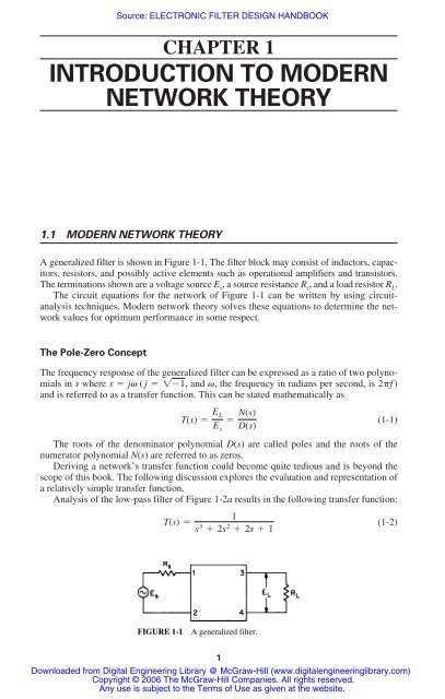
Source: ELECTRONIC FILTER DESIGN HANDBOOKCHAPTER 1INTRODUCTION TO MODERNNETWORK THEORY1.1 MODERN NETWORK THEORYA generalized filter is shown in Figure 1-1. The filter block may consist of inductors, capacitors,resistors, and possibly active elements such as operational amplifiers and transistors.The terminations shown are a voltage source E s , a source resistance R s , and a load resistor R L .The circuit equations for the network of Figure 1-1 can be written by using circuitanalysistechniques. Modern network theory solves these equations to determine the networkvalues for optimum performance in some respect.The Pole-Zero ConceptThe frequency response of the generalized filter can be expressed as a ratio of two polynomialsin s where s jv ( j !1, and v, the frequency in radians per second, is 2pf )and is referred to as a transfer function. This can be stated mathematically as(1-1)The roots of the denominator polynomial D(s) are called poles and the roots of thenumerator polynomial N(s) are referred to as zeros.Deriving a network’s transfer function could become quite tedious and is beyond thescope of this book. The following discussion explores the evaluation and representation ofa relatively simple transfer function.Analysis of the low-pass filter of Figure 1-2a results in the following transfer function:T(s) T(s) E LE s N(s)D(s)1s 3 2s 2 2s 1(1-2)FIGURE 1-1A generalized filter.1Downloaded from Digital Engineering Library @ McGraw-Hill (www.digitalengineeringlibrary.com)Copyright © 2006 The McGraw-Hill Companies. All rights reserved.Any use is subject to the Terms of Use as given at the website.
INTRODUCTION TO MODERN NETWORK THEORY2 CHAPTER ONEFIGURE 1-2 An all-pole n 3 low-pass filter: (a) a filter circuit; and (b) a frequency response.Let us now evaluate this expression at different frequencies after substituting jv for s.The result will be expressed as the absolute magnitude of T( jv) and the relative attentionin decibels with respect to the response at DC.T( jv) 11 2v 2 j(2v v 3 )(1-3)vZT( jv)Z20 log ZT( jv)Z0 1 0 dB1 0.707 3 dB2 0.124 18 dB3 0.0370 29 dB4 0.0156 36 dBThe frequency-response curve is plotted in Figure 1-2b.Analysis of Equation (1-2) indicates that the denominator of the transfer function hasthree roots or poles and the numerator has none. The filter is therefore called an all-poletype. Since the denominator is a third-order polynomial, the filter is also said to havean n 3 complexity. The denominator poles are s 1, s 0.500 j0.866, ands 0.500 j0.866.These complex numbers can be represented as symbols on a complex-number plane.The abscissa is a, the real component of the root, and the ordinate is b, the imaginary part.Each pole is represented as the symbol X, and a zero is represented as 0. Figure 1-3 illustratesthe complex-number plane representation for the roots of Equation (1-2).Certain mathematical restrictions must be applied regarding the location of poles andzeros in order for the filter to be realizable. They must occur in pairs which are conjugatesof each other, except for real-axis poles and zeros, which may occur singly. Poles must alsobe restricted to the left plane (in other words, the real coordinate of the pole must be negative),while zeros may occur in either plane.Synthesis of <strong>Filter</strong>s from Polynomials. Modern network theory has produced families ofstandard transfer functions that provide optimum filter performance in some desiredrespect. Synthesis is the process of deriving circuit component values from these transferfunctions. Chapter 11 contains extensive tables of transfer functions and their associatedcomponent values so that design by synthesis is not required. Also, computer programs onthe CD-ROM simplify the design process. However, in order to gain some understandingDownloaded from Digital Engineering Library @ McGraw-Hill (www.digitalengineeringlibrary.com)Copyright © 2006 The McGraw-Hill Companies. All rights reserved.Any use is subject to the Terms of Use as given at the website.
INTRODUCTION TO MODERN NETWORK THEORYINTRODUCTION TO MODERN NETWORK THEORY 3FIGURE 1-3 A complex-frequency plane representationof Equation (1-2).as to how these values have been determined, we will now discuss a few methods of filtersynthesis.Synthesis by Expansion of Driving-Point Impedance. The input impedance to the generalizedfilter of Figure 1-1 is the impedance seen looking into terminals 1 and 2 with terminals3 and 4 terminated, and is referred to as the driving-point impedance or Z 11 of thenetwork. If an expression for Z 11 could be determined from the given transfer function, thisexpression could then be expanded to define the filter.A family of transfer functions describing the flattest possible shape and a monotonicallyincreasing attenuation in the stopband is known as the Butterworth low-passresponse. These all-pole transfer functions have denominator polynomial roots, which fallon a circle having a radius of unity from the origin of the jv axis. The attenuation for thisfamily is 3 dB at 1 rad/s.The transfer function of Equation (1-2) satisfies this criterion. It is evident fromFigure 1-3 that if a circle were drawn having a radius of 1, with the origin as the center,it would intersect the real root and both complex roots.If R s in the generalized filter of Figure 1-1 is set to 1 , a driving-point impedanceexpression can be derived in terms of the Butterworth transfer function asZ 11 D(s) snD(s) s n(1-4)where D(s) is the denominator polynomial of the transfer function and n is the order of thepolynomial.After D(s) is substituted into Equation (1-4), Z 11 is expanded using the continued fractionexpansion. This expansion involves successive division and inversion of a ratio of twopolynomials. The final form contains a sequence of terms, each alternately representing acapacitor and an inductor and finally the resistive termination. This procedure is demonstratedby the following example.Example 1-1 Synthesis of N 3 Butterworth Low-Pass <strong>Filter</strong> by ContinuedFraction ExpansionRequired:A low-pass LC filter having a Butterworth n 3 response.Downloaded from Digital Engineering Library @ McGraw-Hill (www.digitalengineeringlibrary.com)Copyright © 2006 The McGraw-Hill Companies. All rights reserved.Any use is subject to the Terms of Use as given at the website.
INTRODUCTION TO MODERN NETWORK THEORY4 CHAPTER ONEResult:(a) Use the Butterworth transfer function:T(s) 1s 3 2s 2 2s 1(1-2)(b) Substitute D(s) s 3 2s 2 2s 1 and s n s 3 into Equation (1-4), which results inZ 11 2s 2 2s 12s 3 2s 2 2s 1(1-4)(c) Express Z 11 so that the denominator is a ratio of the higher-order to the lower-orderpolynomial:Z 11 12s 3 2s 2 2s 12s 2 2s 1(d) Dividing the denominator and inverting the remainder results in1Z 11 1s 2s 2 2s 1s 1(e) After further division and inversion, we get as our final expression:1Z 11 1s 2s 1s 1(1-5)The circuit configuration of Figure 1-4 is called a ladder network, since it consistsof alternating series and shunt branches. The input impedance can be expressed as thefollowing continued fraction:1Z 11 1Y 11Z 2Y 3 c 1(1-6)Z n1 1 Y nwhere Y sC and Z sL for the low-pass all-pole ladder except for a resistive terminationwhere Y n sC 1/R L .Downloaded from Digital Engineering Library @ McGraw-Hill (www.digitalengineeringlibrary.com)Copyright © 2006 The McGraw-Hill Companies. All rights reserved.Any use is subject to the Terms of Use as given at the website.
INTRODUCTION TO MODERN NETWORK THEORYINTRODUCTION TO MODERN NETWORK THEORY 5FIGURE 1-4A general ladder network.Figure 1-5 can then be derived from Equation (1-5) and (1-6) by inspection. This canbe proved by reversing the process of expanding Z 11 . By alternately adding admittancesand impedances while working toward the input, Z 11 is verified as being equal toEquation (1-5).Synthesis for Unequal Terminations. If the source resistor is set equal to 1 and theload resistor is desired to be infinite (unterminated), the impedance looking into terminals 1and 2 of the generalized filter of Figure 1-1 can be expressed asZ 11D(s even)D(s odd)(1-7)D(s even) contains all the even-power s terms of the denominator polynomial andD(s odd) consist of all the odd-power s terms of any realizable all-pole low-pass transferfunction. Z 11 is expanded into a continued fraction, as in Example 1-1, to define the circuit.Example 1-2TerminationSynthesis of N 3 Butterworth Low-Pass <strong>Filter</strong> for an InfiniteRequired:Low-pass filter having a Butterworth n 3 response with a source resistance of 1 andan infinite termination.FIGURE 1-5 The low-pass filter for Equation (1-5).Downloaded from Digital Engineering Library @ McGraw-Hill (www.digitalengineeringlibrary.com)Copyright © 2006 The McGraw-Hill Companies. All rights reserved.Any use is subject to the Terms of Use as given at the website.
INTRODUCTION TO MODERN NETWORK THEORY6 CHAPTER ONEResult:(a) Use the Butterworth transfer function:T(s) 1s 3 2s 2 2s 1(1-2)(b) Substitute D(s even) 2s 2 1 and D(s odd) s 3 2s into Equation (1-7):Z 11 2s2 1s 3 2s(1-7)(c) Express Z 11 so that the denominator is a ratio of the higher- to the lower-orderpolynomial:Z 11 1s 3 2s2s 2 1(d) Dividing the denominator and inverting the remainder results in1Z 11 10.5s 2s 2 11.5s(e) Dividing and further inverting results in the final continued fraction:The circuit is shown in Figure 1-6.1Z 11 10.5s 1.333s 11.5s(1-8)Synthesis by Equating Coefficients. An active three-pole low-pass filter is shown inFigure 1-7. Its transfer function is given byT(s) 1s 3 A s 2 B sC 1(1-9)where A C 1 C 2 C 3 (1-10)B 2C 3 (C 1 C 2 ) (1-11)and C C 2 3C 3 (1-12)FIGURE 1-6 The low-pass filter of Example 1-2.Downloaded from Digital Engineering Library @ McGraw-Hill (www.digitalengineeringlibrary.com)Copyright © 2006 The McGraw-Hill Companies. All rights reserved.Any use is subject to the Terms of Use as given at the website.
INTRODUCTION TO MODERN NETWORK THEORYINTRODUCTION TO MODERN NETWORK THEORY 7FIGURE 1-7The general n 3 active low-pass filter.If a Butterworth transfer function is desired, we can set Equation (1-9) equal toEquation (1-2).T(s) By equating coefficients, we obtain1s 3 A s 2 B sC 1 1s 3 2s 2 2s 1A 1B 2C 2(1-13)Substituting these coefficients in Equation (1-10) through (1-12) and solving for C 1 , C 2 ,and C 3 results in the circuit of Figure 1-8.Synthesis of filters directly from polynomials offers an elegant solution to filter design.However, it also may involve laborious computations to determine circuit element values.<strong>Design</strong> methods have been greatly simplified by the curves, tables, computer programs, andstep-by-step procedures provided in this handbook, so design by synthesis can be left to theadvanced specialist.Active vs. Passive <strong>Filter</strong>s. The LC filters of Figures 1-5 and 1-6 and the active filter ofFigure 1-8 all satisfy an n 3 Butterworth low-pass transfer function. The filter designeris frequently faced with the sometimes difficult decision of choosing whether to use anactive or LC design. A number of factors must be considered. Some of the limitations andconsiderations for each filter type will now be discussed.Frequency Limitations. At subaudio frequencies, LC filter designs require high valuesof inductance and capacitance along with their associated bulk. Active filters are morepractical because they can be designed at higher impedance levels so that capacitor magnitudesare reduced.Above 20 MHz or so, most commercial-grade operational amplifiers have insufficientopen-loop gain for the average active filter requirement. However, amplifiers are availableFIGURE 1-8A Butterworth n 3 active low-pass filter.Downloaded from Digital Engineering Library @ McGraw-Hill (www.digitalengineeringlibrary.com)Copyright © 2006 The McGraw-Hill Companies. All rights reserved.Any use is subject to the Terms of Use as given at the website.
INTRODUCTION TO MODERN NETWORK THEORY8 CHAPTER ONEwith extended bandwidth at an increased cost so that active filters at frequencies up to100 MHz are possible. LC filters, on the other hand, are practical at frequencies up to afew hundred megahertz. Beyond this range, filters become impractical to build in lumpedform, and so distributed parameter techniques are used, such as stripline or microstrip,where a PC board functions as a distributed transmission line.Size Considerations. Active filters are generally smaller than their LC counterpartssince inductors are not required. Further reduction in size is possible with microelectronictechnology. Surface mount components for the most part have replaced Hybrid technology,whereas in the past Hybrids were the only way to reduce the size of active filters.Economics and Ease of Manufacture. LC filters generally cost more than active filtersbecause they use inductors. High-quality coils require efficient magnetic cores. Sometimes,special coil-winding methods are needed as well. These factors lead to the increased costof LC filters.Active filters have the distinct advantage that they can be easily assembled using standardoff-the-shelf components. LC filters require coil-winding and coil-assembly skills. Inaddition, eliminating inductors prevents magnetic emissions, which can be troublesome.Ease of Adjustment. In critical LC filters, tuned circuits require adjustment to specificresonances. Capacitors cannot be made variable unless they are below a few hundred picofarads.Inductors, however, can easily be adjusted, since most coil structures provide ameans for tuning, such as an adjustment slug for a Ferrite potcore.Many active filter circuits are not easily adjustable, however. They may contain RC sectionswhere two or more resistors in each section have to be varied in order to control resonance.These types of circuit configurations are avoided. The active filter design techniquespresented in this handbook include convenient methods for adjusting resonances whererequired, such as for narrowband bandpass filters.BIBLIOGRAPHYGuillemin, E. A. (1957). Introduction to Circuit Theory. New York: John Wiley and Sons.Stewart, J. L. (1956). Circuit Theory and <strong>Design</strong>. New York: John Wiley and Sons.White Electromagnetics. (1963). A <strong>Handbook</strong> on Electrical <strong>Filter</strong>s. White Electromagnetics, Inc.Downloaded from Digital Engineering Library @ McGraw-Hill (www.digitalengineeringlibrary.com)Copyright © 2006 The McGraw-Hill Companies. All rights reserved.Any use is subject to the Terms of Use as given at the website.
Source: ELECTRONIC FILTER DESIGN HANDBOOKCHAPTER 2SELECTING THE RESPONSECHARACTERISTIC2.1 FREQUENCY-RESPONSE NORMALIZATIONSeveral parameters are used to characterize a filter’s performance. The most commonlyspecified requirement is frequency response. When given a frequency-response specification,the engineer must select a filter design that meets these requirements. This is accomplishedby transforming the required response to a normalized low-pass specificationhaving a cutoff of 1 rad/s. This normalized response is compared with curves of normalizedlow-pass filters which also have a 1-rad/s cutoff. After a satisfactory low-pass filter isdetermined from the curves, the tabulated normalized element values of the chosen filterare transformed or denormalized to the final design.Modern network theory has provided us with many different shapes of amplitude versusfrequency which have been analytically derived by placing various restrictions ontransfer functions. The major categories of these low-pass responses are• Butterworth• Chebyshev• Linear Phase• Transitional• Synchronously tuned• Elliptic-functionWith the exception of the elliptic-function family, these responses are all normalizedto a 3-dB cutoff of 1 rad/s.Frequency and Impedance ScalingThe basis for normalization of filters is the fact that a given filter’s response can be scaled(shifted) to a different frequency range by dividing the reactive elements by a frequencyscalingfactor (FSF). The FSF is the ratio of a reference frequency of the desired responseto the corresponding reference frequency of the given filter. Usually 3-dB points areselected as reference frequencies of low-pass and high-pass filters, and the center frequencyis chosen as the reference for bandpass filters. The FSF can be expressed asFSF desired reference frequencyexisting reference frequency(2-1)9Downloaded from Digital Engineering Library @ McGraw-Hill (www.digitalengineeringlibrary.com)Copyright © 2006 The McGraw-Hill Companies. All rights reserved.Any use is subject to the Terms of Use as given at the website.
SELECTING THE RESPONSE CHARACTERISTIC10 CHAPTER TWOThe FSF must be a dimensionless number; so both the numerator and denominator ofEquation (2-1) must be expressed in the same units, usually radians per second. The followingexample demonstrates the computation of the FSF and frequency scaling of filters.Example 2-1Frequency Scaling of a Low-Pass <strong>Filter</strong>Required:A low-pass filter, either LC or active, with an n 3 Butterworth transfer function havinga 3-dB cutoff at 1000 Hz.Result:Figure 2-1 illustrates the LC and active n 3 Butterworth low-pass filters discussed inChapter 1 and their response.(a) Compute FSF.FSF 2p1000 rad/s1 rad/s 6280(2-1)(b) Dividing all the reactive elements by the FSF results in the filters of Figure 2-2aand b and the response of Figure 2-2c.Note that all points on the frequency axis of the normalized response have been multipliedby the FSF. Also, since the normalized filter has its cutoff at 1 rad/s, the FSF canbe directly expressed by 2pf c , where is the desired low-pass cutoff frequency in hertz.f cFrequency scaling a filter has the effect of multiplying all points on the frequency axisof the response curve by the FSF. Therefore, a normalized response curve can be directlyused to predict the attenuation of the denormalized filter.FIGURE 2-1n 3 Butterworth low-pass filter: (a) LC filter; (b) active filter; and (c) frequency response.Downloaded from Digital Engineering Library @ McGraw-Hill (www.digitalengineeringlibrary.com)Copyright © 2006 The McGraw-Hill Companies. All rights reserved.Any use is subject to the Terms of Use as given at the website.
SELECTING THE RESPONSE CHARACTERISTICSELECTING THE RESPONSE CHARACTERISTIC 11FIGURE 2-2 The denormalized low-pass filter of Example 2-1: (a) LC filter; (b) active filter; and (c) frequencyresponse.When the filters of Figure 2-1 were denormalized to those of Figure 2-2, the transferfunction changed as well. The denormalized transfer function became1T(s) (2-2)4.03 10 12 s 3 5.08 10 9 s 2 3.18 10 4 s 1The denominator has roots:s 6280, s 3140 j5438, and s 3140 j5438.These roots can be obtained directly from the normalized roots by multiplying the normalizedroot coordinates by the FSF. Frequency scaling a filter also scales the poles andzeros (if any) by the same factor.The component values of the filters in Figure 2-2 are not very practical. The capacitorvalues are much too large and the 1- resistor values are not very desirable. This situationcan be resolved by impedance scaling. Any linear active or passive network maintains itstransfer function if all resistor and inductor values are multiplied by an impedance-scalingfactor Z, and all capacitors are divided by the same factor Z. This occurs because the Zs cancelin the transfer function. To prove this, let’s investigate the transfer function of the simpletwo-pole low-pass filter of Figure 2-3a, which is1T(s) (2-3)s 2 LC sCR 1Impedance scaling can be mathematically expressed asRr ZRLr ZL(2-4)(2-5)Cr C Z(2-6)where the primes denote the values after impedance scaling.Downloaded from Digital Engineering Library @ McGraw-Hill (www.digitalengineeringlibrary.com)Copyright © 2006 The McGraw-Hill Companies. All rights reserved.Any use is subject to the Terms of Use as given at the website.
SELECTING THE RESPONSE CHARACTERISTIC12 CHAPTER TWOFIGURE 2-3 A two-pole low-pass LC filter: (a) a basic filter; and (b) animpedance-scaled filter.If we impedance-scale the filter, we obtain the circuit of Figure 2-3b. The new transferfunction then becomes1T(s) s 2 ZL C Z sC Z ZR 1(2-7)Clearly, the Zs cancel, so both transfer functions are equivalent.We can now use impedance scaling to make the values in the filters of Figure 2-2 morepractical. If we use impedance scaling with a Z of 1000, we obtain the filters of Figure 2-4.The values are certainly more suitable.Frequency and impedance scaling are normally combined into one step rather than performedsequentially. The denormalized values are then given byRr R ZLr L ZFSFCCr FSF Zwhere the primed values are both frequency- and impedance-scaled.(2-8)(2-9)(2-10)Low-Pass Normalization. In order to use normalized low-pass filter curves and tables, agiven low-pass filter requirement must first be converted into a normalized requirement.The curves can now be entered to find a satisfactory normalized filter which is then scaledto the desired cutoff.The first step in selecting a normalized design is to convert the requirement into a steepnessfactor A s , which can be defined asA s f sf c(2-11)FIGURE 2-4The impedance-scaled filters of Example 2-1: (a) LC filter; and (b) active filter.Downloaded from Digital Engineering Library @ McGraw-Hill (www.digitalengineeringlibrary.com)Copyright © 2006 The McGraw-Hill Companies. All rights reserved.Any use is subject to the Terms of Use as given at the website.
SELECTING THE RESPONSE CHARACTERISTICSELECTING THE RESPONSE CHARACTERISTIC 13where f s is the frequency having the minimum required stopband attenuation and f c is thelimiting frequency or cutoff of the passband, usually the 3-dB point. The normalized curvesare compared with A s , and a design is selected that meets or exceeds the requirement. Thedesign is often frequency scaled so that the selected passband limit of the normalized designoccurs at f c .If the required passband limit f c is defined as the 3-dB cutoff, the steepness factor A s canbe directly looked up in radians per second on the frequency axis of the normalized curves.Suppose that we required a low-pass filter that has a 3-dB point at 100 Hz and more than30-dB attenuation at 400 Hz. A normalized low-pass filter that has its 3-dB point at 1 rad/sand over 30-dB attenuation at 4 rad/s would meet the requirement if the filter werefrequency-scaled so that the 3-dB point occurred at 100 Hz. Then there would be over30-dB attenuation at 400 Hz, or four times the cutoff, because a response shape is retainedwhen a filter is frequency scaled.The following example demonstrates normalizing a simple low-pass requirement.Example 2-2Normalizing a Low-Pass Specification for a 3-dB cutoffRequired:Normalize the following specification:A low-pass filter3 dB at 200 Hz30-dB minimum at 800 HzResult:(a) Compute A s .(b) Normalized requirement:3 dB at 1 rad/s30-dB minimum at 4 rad/sA s f s 800 Hzf c200 Hz 4(2-11)In the event f c does not correspond to the 3-dB cutoff, A s can still be computed and anormalized design found that will meet the specifications. This is illustrated in the followingexample.Example 2-3Normalizing a Low-Pass Specification for a 1-dB cutoffRequired:Normalize the following specification:A low-pass filter1 dB at 200 Hz30-dB minimum at 800 HzResult:(a) Compute A s .A s f s 800 Hzf c200 Hz 4(2-11)Downloaded from Digital Engineering Library @ McGraw-Hill (www.digitalengineeringlibrary.com)Copyright © 2006 The McGraw-Hill Companies. All rights reserved.Any use is subject to the Terms of Use as given at the website.
SELECTING THE RESPONSE CHARACTERISTIC14 CHAPTER TWO(b) Normalized requirement:1 dB at K rad/s30-dB minimum at 4 K rad/s(where K is arbitrary)A possible solution to Example 2-3 would be a normalized filter which has a 1-dB pointat 0.8 rad/s and over 30 dB attenuation at 3.2 rad/s. The fundamental requirement is that thenormalized filter makes the transition between the passband and stopband limits within afrequency ratio A s .High-Pass Normalization. A normalized n 3 low-pass Butterworth transfer functionwas given in section 1.1 asT(s) 1s 3 2s 2 2s 1and the results of evaluating this transfer function at various frequencies were(1-2)vu T(jv)u20 log u T(jv)u0 1 0 dB1 0.7073 dB2 0.12418 dB3 0.037029 dB4 0.0156 36 dBLet’s now perform a high-pass transformation by substituting 1/s for s in Equation (1-2).After some algebraic manipulations, the resulting transfer function becomesT(s) s 3s 3 2s 2 2s 1(2-12)If we evaluate this expression at specific frequencies, we can generate the followingtable:vu T(jv)u20 log u T(jv)u0.25 0.0156 36 dB0.333 0.0370 29 dB0.500 0.12418 dB1 0.7073 dB` 1 0 dBThe response is clearly that of a high-pass filter. It is also apparent that the low-passattenuation values now occur at high-pass frequencies that are exactly the reciprocals of thecorresponding low-pass frequencies. A high-pass transformation of a normalized low-passfilter transposes the low-pass attenuation values to reciprocal frequencies and retains the3-dB cutoff at 1 rad/s. This relationship is evident in Figure 2-5, where both filter responsesare compared.Downloaded from Digital Engineering Library @ McGraw-Hill (www.digitalengineeringlibrary.com)Copyright © 2006 The McGraw-Hill Companies. All rights reserved.Any use is subject to the Terms of Use as given at the website.
SELECTING THE RESPONSE CHARACTERISTICSELECTING THE RESPONSE CHARACTERISTIC 15FIGURE 2-5A normalized low-pass high-pass relationship.The normalized low-pass curves could be interpreted as normalized high-pass curves byreading the attenuation as indicated and taking the reciprocals of the frequencies. However,it is much easier to convert a high-pass specification into a normalized low-pass requirementand use the curves directly.To normalize a high-pass filter specification, calculate A s , which in the case of high-passfilters is given byA s f cf s(2-13)Since the A s , for high-pass filters is defined as the reciprocal of the A s for low-pass filters,Equation (2-13) can be directly interpreted as a low-pass requirement. A normalizedlow-pass filter can then be selected from the curves. A high-pass transformation is performedon the corresponding low-pass filter, and the resulting high-pass filter is scaled tothe desired cutoff frequency.The following example shows the normalization of a high-pass filter requirement.Example 2-4Normalizing a High-Pass SpecificationRequired:Normalize the following requirement:A high-pass filter3 dB at 200 Hz30-dB minimum at 50 HzResult:(a) Compute A s .A s f c 200 Hzf s 50 Hz 4(2-13)Downloaded from Digital Engineering Library @ McGraw-Hill (www.digitalengineeringlibrary.com)Copyright © 2006 The McGraw-Hill Companies. All rights reserved.Any use is subject to the Terms of Use as given at the website.
SELECTING THE RESPONSE CHARACTERISTIC16 CHAPTER TWO(b) Normalized equivalent low-pass requirement:3 dB at 1 rad/s30-dB minimum at 4 rad/sBandpass Normalization. Bandpass filters fall into two categories: narrowband andwideband. If the ratio of the upper cutoff frequency to the lower cutoff frequency is over 2(an octave), the filter is considered a wideband type.Wideband Bandpass <strong>Filter</strong>s. Wideband filter specifications can be separated into individuallow-pass and high-pass requirements which are treated independently. The resultinglow-pass and high-pass filters are then cascaded to meet the composite response.Example 2-5Normalizing a Wideband Bandpass <strong>Filter</strong>Required:Normalize the following specification:bandpass filter3 dB at 500 and 1000 Hz40-dB minimum at 200 and 2000 HzResult:(a) Determine the ratio of upper cutoff to lower cutoff.1000 Hz500 Hz 2wideband type(b) Separate requirement into individual specifications.High-pass filter:Low-pass filter:3 dB at 500 Hz 3 dB at 1000 Hz40-dB minimum at 200 Hz 40-dB minimum at 2000 HzA s 2.5 (2-13) A s 2.0 (2-11)(c) Normalized high-pass and low-pass filters are now selected, scaled to the requiredcutoff frequencies, and cascaded to meet the composite requirements. Figure 2-6shows the resulting circuit and response.Narrowband Bandpass <strong>Filter</strong>s. Narrowband bandpass filters have a ratio of upper cutofffrequency to lower cutoff frequency of approximately 2 or less and cannot be designedas separate low-pass and high-pass filters. The major reason for this is evident from Figure2-7. As the ratio of upper cutoff to lower cutoff decreases, the loss at the center frequencywill increase, and it may become prohibitive for ratios near unity.If we substitute s 1/s for s in a low-pass transfer function, a bandpass filter results.The center frequency occurs at 1 rad/s, and the frequency response of the low-pass filter isdirectly transformed into the bandwidth of the bandpass filter at points of equivalent attenuation.In other words, the attenuation bandwidth ratios remain unchanged. This is shownin Figure 2-8, which shows the relationship between a low-pass filter and its transformedbandpass equivalent. Each pole and zero of the low-pass filter is transformed into a pair ofpoles and zeros in the bandpass filter.Downloaded from Digital Engineering Library @ McGraw-Hill (www.digitalengineeringlibrary.com)Copyright © 2006 The McGraw-Hill Companies. All rights reserved.Any use is subject to the Terms of Use as given at the website.
SELECTING THE RESPONSE CHARACTERISTICSELECTING THE RESPONSE CHARACTERISTIC 17FIGURE 2-6 The results of Example 2-5: (a) cascade oflow-pass and high-pass filters; and (b) frequency response.In order to design a bandpass filter, the following sequence of steps is involved.1. Convert the given bandpass filter requirement into a normalized low-pass specification.2. Select a satisfactory low-pass filter from the normalized frequency-response curves.3. Transform the normalized low-pass parameters into the required bandpass filter.FIGURE 2-7 Limitations of the wideband approach for narrowband filters: (a) a cascadeof low-pass and high-pass filters; (b) a composite response; and (c) algebraic sumof attenuation.Downloaded from Digital Engineering Library @ McGraw-Hill (www.digitalengineeringlibrary.com)Copyright © 2006 The McGraw-Hill Companies. All rights reserved.Any use is subject to the Terms of Use as given at the website.
SELECTING THE RESPONSE CHARACTERISTIC18 CHAPTER TWOFIGURE 2-8A low-pass to bandpass transformation.The response shape of a bandpass filter is shown in Figure 2-9, along with some basicterminology. The center frequency is defined asf 0 2f L f u(2-14)where f L is the lower passband limit and f u is the upper passband limit, usually the 3-dBattenuation frequencies. For the more general casef 02f 1f 2(2-15)where f 1 and f 2 are any two frequencies having equal attenuation. These relationships implygeometric symmetry; that is, the entire curve below f 0 is the mirror image of the curveabove f 0 when plotted on a logarithmic frequency axis.An important parameter of bandpass filters is the filter selectivity factor or Q, which isdefined asQ f 0BW(2-16)where BW is the passband bandwidth or f u f L.Downloaded from Digital Engineering Library @ McGraw-Hill (www.digitalengineeringlibrary.com)Copyright © 2006 The McGraw-Hill Companies. All rights reserved.Any use is subject to the Terms of Use as given at the website.
SELECTING THE RESPONSE CHARACTERISTICSELECTING THE RESPONSE CHARACTERISTIC 19FIGURE 2-9shape.A general bandpass filter responseAs the filter Q increases, the response shape near the passband approaches the arithmeticallysymmetrical condition which is mirror-image symmetry near the center frequency,when plotted using a linear frequency axis. For Qs of 10 or more, the centerfrequency can be redefined as the arithmetic mean of the passband limits, so we can replaceEquation (2-14) withf 0 f L f u2(2-17)In order to utilize the normalized low-pass filter frequency-response curves, a given narrowbandbandpass filter specification must be transformed into a normalized low-passrequirement. This is accomplished by first manipulating the specification to make it geometricallysymmetrical. At equivalent attenuation points, corresponding frequencies aboveand below f 0 must satisfyf 1f 2 f 2 0(2-18)which is an alternate form of Equation (2-15) for geometric symmetry. The given specificationis modified by calculating the corresponding opposite geometric frequency for eachstopband frequency specified. Each pair of stopband frequencies will result in two new frequencypairs. The pair having the lesser separation is retained, since it represents the moresevere requirement.A bandpass filter steepness factor can now be defined asA sstopband bandwidthpassband bandwidth(2-19)This steepness factor is used to select a normalized low-pass filter from the frequencyresponsecurves that makes the passband to stopband transition within a frequency ratioof A s .Downloaded from Digital Engineering Library @ McGraw-Hill (www.digitalengineeringlibrary.com)Copyright © 2006 The McGraw-Hill Companies. All rights reserved.Any use is subject to the Terms of Use as given at the website.
SELECTING THE RESPONSE CHARACTERISTIC20 CHAPTER TWOThe following example shows the normalization of a bandpass filter requirement.Example 2-6Normalizing a Bandpass <strong>Filter</strong> RequirementRequired:Normalize the following bandpass filter requirement:A bandpass filterA center frequency of 100 Hz3 dB at 15 Hz (85 Hz, 115 Hz)40 dB at 30 Hz (70 Hz, 130 Hz)Result:(a) First, compute the center frequency f 0 .f 0 2f L f u285 115 98.9 Hz(2-14)(b) Compute two geometrically related stopband frequency pairs for each pair of stopbandfrequencies given.Let f 1 70 Hz.f 2 f 2 0 (98.9)2 139.7 Hzf 170(2-18)Let f 2 130 Hz.f 1 f 2 0 (98.9)2 75.2 Hzf 2130(2-18)The two pairs aref 1 70 Hz, f 2 139.7 Hz ( f 2 f 1 69.7 Hz)andf 1 75.2 Hz, f 2 130 Hz ( f 2 f 1 54.8 Hz)Retain the second frequency pair, since it has the lesser separation. Figure 2-10compares the specified filter requirement and the geometrically symmetricalequivalent.(c) Calculate A s .A s stopband bandwidth 54.8 Hzpassband bandwidth 30 Hz 1.83(2-19)(d) A normalized low-pass filter can now be selected from the normalized curves.Since the passband limit is the 3-dB point, the normalized filter is required to haveover 40 dB of rejection at 1.83 rad/s or 1.83 times the 1-rad/s cutoff.The results of Example 2-6 indicate that when frequencies are specified in an arithmeticallysymmetrical manner, the narrower stopband bandwidth can be directly computed byBW stopband f 2 f 2 0f 2(2-20)Downloaded from Digital Engineering Library @ McGraw-Hill (www.digitalengineeringlibrary.com)Copyright © 2006 The McGraw-Hill Companies. All rights reserved.Any use is subject to the Terms of Use as given at the website.
SELECTING THE RESPONSE CHARACTERISTICSELECTING THE RESPONSE CHARACTERISTIC 21FIGURE 2-10 The frequency-response requirements ofExample 2-6: (a) a given filter requirement; and (b) a geometricallysymmetrical requirement.The narrower stopband bandwidth corresponds to the more stringent value of A s , thesteepness factor.It is sometimes desirable to compute two geometrically related frequencies that correspondto a given bandwidth. Upon being given the center frequency f 0 and the bandwidthBW, the lower and upper frequencies are respectively computed byf 1 a BW 2Å 2 b f 2 0 BW 2(2-21)f 2 a BW 2Å 2 b f 2 0 BW 2(2-22)Use of these formulas is illustrated in the following example.Example 2-7Determining Bandpass <strong>Filter</strong> Bandwidths at Equal Attenuation PointsRequired:For a bandpass filter having a center frequency of 10 kHz, determine the frequenciescorresponding to bandwidths of 100 Hz, 500 Hz, and 2000 Hz.Downloaded from Digital Engineering Library @ McGraw-Hill (www.digitalengineeringlibrary.com)Copyright © 2006 The McGraw-Hill Companies. All rights reserved.Any use is subject to the Terms of Use as given at the website.
SELECTING THE RESPONSE CHARACTERISTIC22 CHAPTER TWOResult:Compute f 1 and f 2 for each bandwidth, usingf 1 a BW 2Å 2 b f 2 0 BW 2(2-21)f 2 a BW 2Å 2 b f 2 0 BW 2(2-22)BW, Hz f 1 , Hz F 2 , Hz100 9950 10,050500 9753 10,2532000 9050 11,050The results of Example 2-7 indicate that for narrow percentage bandwidths (1 percent)f 1 and f 2 are arithmetically spaced about f 0 . For the wider cases, the arithmetic center of f 1and f 2 would be slightly above the actual geometric center frequency f 0 . Another and moremeaningful way of stating the converse is that for a given pair of frequencies, the geometricmean is below the arithmetic mean.Bandpass filter requirements are not always specified in an arithmetically symmetricalmanner as in the previous examples. Multiple stopband attenuation requirements may alsoexist. The design engineer is still faced with the basic problem of converting the given parametersinto geometrically symmetrical characteristics so that a steepness factor (or factors)can be determined. The following example demonstrates the conversion of a specificationsomewhat more complicated than the previous example.Example 2-8Normalizing a Non-Symmetrical Bandpass <strong>Filter</strong> RequirementRequired:Normalize the following bandpass filter specification:bandpass filter1-dB passband limits of 12 kHz and 14 kHz20-dB minimum at 6 kHz30-dB minimum at 4 kHz40-dB minimum at 56 kHzResult:(a) First, compute the center frequency, usingf L 12 kHzf 0 12.96 kHzf u 14 kHz(2-14)(b) Compute the corresponding geometric frequency for each stopband frequencygiven, using Equation (2-18).f 1 f 2 f 2 0(2-18)Downloaded from Digital Engineering Library @ McGraw-Hill (www.digitalengineeringlibrary.com)Copyright © 2006 The McGraw-Hill Companies. All rights reserved.Any use is subject to the Terms of Use as given at the website.
SELECTING THE RESPONSE CHARACTERISTICSELECTING THE RESPONSE CHARACTERISTIC 23FIGURE 2-11 The given and transformed responses ofExample 2-7: (a) a given requirement; and (b) geometricallysymmetrical response.Figure 2-11 illustrates the comparison between the given requirement and the correspondinggeometrically symmetrical equivalent response.f 1 f 26 kHz 28 kHz4 kHz 42 kHz3 kHz 56 kHz(c) Calculate the steepness factor for each stopband bandwidth in Figure 2-11b.22 kHz20 dB: A s (2-19)2 kHz 1130 dB:40 dB:A s A s 38 kHz2 kHz 1953 kHz2 kHz 26.5(d) Select a low-pass filter from the normalized tables. A filter is required that has over20, 30, and 40 dB of rejection at, respectively, 11, 19, and 26.5 times its 1-dB cutoff.Downloaded from Digital Engineering Library @ McGraw-Hill (www.digitalengineeringlibrary.com)Copyright © 2006 The McGraw-Hill Companies. All rights reserved.Any use is subject to the Terms of Use as given at the website.
SELECTING THE RESPONSE CHARACTERISTIC24 CHAPTER TWOBand-Reject NormalizationWideband Band-Reject <strong>Filter</strong>s. Normalizing a band-reject filter requirementproceeds along the same lines as for a bandpass filter. If the ratio of the upper cutofffrequency to the lower cutoff frequency is an octave or more, a band-reject filter requirementcan be classified as wideband and separated into individual low-pass and high-passspecifications. The resulting filters are paralleled at the input and combined at the output.The following example demonstrates normalization of a wideband band-reject filterrequirement.Example 2-9Normalizing a Wideband Band-Reject <strong>Filter</strong>Required:A band-reject filter3 dB at 200 and 800 Hz40-dB minimum at 300 and 500 HzResult:(a) Determine the ratio of upper cutoff to lower cutoff, using800 Hz200 Hz 4wideband type(b) Separate requirements into individual low-pass and high-pass specifications.Low-pass filter:High-pass filter:3 dB at 200 Hz 3 dB at 800 Hz40-dB minimum at 300 Hz 40-dB minimum at 500 HzA s 1.5 (2-11) A s 1.6 (2-13)(c) Select appropriate filters from the normalized curves and scale the normalized lowpassand high-pass filters to cutoffs of 200 Hz and 800 Hz, respectively. Figure 2-12shows the resulting circuit and response.The basic assumption of the previous example is that when the filter outputs are combined,the resulting response is the superimposed individual response of both filters. Thisis a valid assumption if each filter has sufficient rejection in the band of the other filter sothat there is no interaction when the outputs are combined. Figure 2-13 shows the casewhere inadequate separation exists.The requirement for a minimum separation between cutoffs of an octave or more is byno means rigid. Sharper filters can have their cutoffs placed closer together with minimalinteraction.Narrowband Band-Reject <strong>Filter</strong>s. The normalized transformation described for bandpassfilters where s 1/s is substituted into a low-pass transfer function can instead beapplied to a high-pass transfer function to obtain a band-reject filter. Figure 2-14 shows thedirect equivalence between a high-pass filter’s frequency response and the transformedband-reject filter’s bandwidth.Downloaded from Digital Engineering Library @ McGraw-Hill (www.digitalengineeringlibrary.com)Copyright © 2006 The McGraw-Hill Companies. All rights reserved.Any use is subject to the Terms of Use as given at the website.
SELECTING THE RESPONSE CHARACTERISTICSELECTING THE RESPONSE CHARACTERISTIC 25FIGURE 2-12 The results of Example 2-9: (a) combined low-passand high-pass filters; and (b) a frequency response.FIGURE 2-13 Limitations of the wideband band-reject design approach: (a) combined low-pass andhigh-pass filters; (b) composite response; and (c) combined response by the summation of outputs.Downloaded from Digital Engineering Library @ McGraw-Hill (www.digitalengineeringlibrary.com)Copyright © 2006 The McGraw-Hill Companies. All rights reserved.Any use is subject to the Terms of Use as given at the website.
SELECTING THE RESPONSE CHARACTERISTIC26 CHAPTER TWOFIGURE 2-14The relationship between band-reject and high-pass filters.The design method for narrowband band-reject filters can be defined as follows:1. Convert the band-reject requirement directly into a normalized low-pass specification.2. Select a low-pass filter (from the normalized curves) that meets the normalizedrequirements.3. Transform the normalized low-pass parameters into the required band-reject filter. Thismay involve designing the intermediate high-pass filter, or the transformation may bedirect.The band-reject response has geometric symmetry just as bandpass filters have. Figure2-15 defines this response shape. The parameters shown have the same relationship to eachother as they do for bandpass filters. The attenuation at the center frequency is theoreticallyinfinite since the response of a high-pass filter at DC has been transformed to the centerfrequency.FIGURE 2-15The band-reject response.Downloaded from Digital Engineering Library @ McGraw-Hill (www.digitalengineeringlibrary.com)Copyright © 2006 The McGraw-Hill Companies. All rights reserved.Any use is subject to the Terms of Use as given at the website.
SELECTING THE RESPONSE CHARACTERISTICSELECTING THE RESPONSE CHARACTERISTIC 27The geometric center frequency can be defined asf 0 2f L f u(2-14)where f L and f u are usually the 3-dB frequencies, or for the more general case:f 0 2f 1 f 2(2-15)The selectivity factor Q is defined asQ f 0BW(2-16)where BW is f u f L . For Qs of 10 or more, the response near the center frequencyapproaches the arithmetically symmetrical condition, so we can then statef 0 f L f u2(2-17)To use the normalized curves for the design of a band-reject filter, the response requirementmust be converted to a normalized low-pass filter specification. In order to accomplishthis, the band-reject specification should first be made geometrically symmetrical—that is,each pair of frequencies having equal attenuation should satisfy(2-18)which is an alternate form of Equation (2-15). When two frequencies are specified at a particularattenuation level, two frequency pairs will result from calculating the correspondingopposite geometric frequency for each frequency specified. Retain the pair having thewider separation since it represents the more severe requirement. In the bandpass case, thepair having the lesser separation represented the more difficult requirement.The band-reject filter steepness factor is defined byA s f 1f 2 f 2 0passband bandwidthstopband bandwidth(2-23)A normalized low-pass filter can now be selected that makes the transition from thepassband attenuation limit to the minimum required stopband attenuation within a frequencyratio A s .The following example demonstrates the normalization procedure for a band-reject filter.Example 2-10Normalizing a Narrowband Band-Reject <strong>Filter</strong>Required:band-reject filtercenter frequency of 1000 Hz3 dB at 300 Hz (700 Hz, 1300 Hz)40 dB at 200 Hz (800 Hz, 1200 Hz)Result:(a) First, compute the center frequency f 0 .f 0 2f L f u 2700 1300 954 Hz(2-14)Downloaded from Digital Engineering Library @ McGraw-Hill (www.digitalengineeringlibrary.com)Copyright © 2006 The McGraw-Hill Companies. All rights reserved.Any use is subject to the Terms of Use as given at the website.
SELECTING THE RESPONSE CHARACTERISTIC28 CHAPTER TWO(b) Compute two geometrically related stopband frequency pairs for each pair of stopbandfrequencies given:Let f 1 800 Hzf 2 f 2 0 (954)2 1138 Hzf 1800(2-18)Let f 2 1200 Hzf 1 f 2 0 (954)2 758 Hzf 21200(2-18)The two pairs areandf 1 800 Hz, f 2 1138 Hz ( f 2 f 1 338 Hz)f 1 758 Hz, f 2 1200 Hz ( f 2 f 1 442 Hz)Retain the second pair since it has the wider separation and represents the moresevere requirement. The given response requirement and the geometrically symmetricalequivalent are compared in Figure 2-16(c) Calculate A s .A s passband bandwidth 600 Hzstopband bandwidth 442 Hz 1.36(2-23)FIGURE 2-16 The response of Example 2-10: (a) given requirement;and (b) geometrically symmetrical response.Downloaded from Digital Engineering Library @ McGraw-Hill (www.digitalengineeringlibrary.com)Copyright © 2006 The McGraw-Hill Companies. All rights reserved.Any use is subject to the Terms of Use as given at the website.
SELECTING THE RESPONSE CHARACTERISTICSELECTING THE RESPONSE CHARACTERISTIC 29(d) Select a normalized low-pass filter from the normalized curves that makes the transitionfrom the 3-dB point to the 40-dB point within a frequency ratio of 1.36. Sincethese curves are all normalized to 3 dB, a filter is required with over 40 dB of rejectionat 1.36 rad/s.2.2 TRANSIENT RESPONSEIn our previous discussions of filters, we have restricted our interest to frequency-domainparameters such as frequency response. The input forcing function was a sine wave. In realworldapplications of filters, input signals consist of a variety of complex waveforms. Theresponse of filters to these nonsinusoidal inputs is called transient response.A filter’s transient response is best evaluated in the time domain since we are usuallydealing with input signals which are functions of time, such as pulses or amplitude steps.The frequency- and time-domain parameters of a filter are directly related through theFourier or Laplace transforms.The Effect of Nonuniform Time DelayEvaluating a transfer function as a function of frequency results in both a magnitude andphase characteristic. Figure 2-17 shows the amplitude and phase response of a normalizedn 3 Butterworth low-pass filter. Butterworth low-pass filters have a phase shift ofexactly n times 45 at the 3-dB frequency. The phase shift continuously increases as thetransition is made into the stopband and eventually approaches n times 90 at frequenciesfar removed from the passband. Since the filter described by Figure 2-17 has a complexityof n 3, the phase shift is 135 at the 3-dB cutoff and approaches 270 in the stopband.Frequency scaling will transpose the phase characteristics to a new frequency rangeas determined by the FSF.It is well known that a square wave can be represented by a Fourier series of odd harmoniccomponents, as indicated in Figure 2-18. Since the amplitude of each harmonic isreduced as the harmonic order increases, only the first few harmonics are of significance.If a square wave is applied to a filter, the fundamental and its significant harmonics musthave a proper relative amplitude relationship at the filter’s output in order to retain thesquare waveshape. In addition, these components must not be displaced in time withrespect to each other. Let’s now consider the effect of a low-pass filter’s phase shift on asquare wave.FIGURE 2-17 The amplitude and phase response of an n 3 Butterworth low-pass filter.Downloaded from Digital Engineering Library @ McGraw-Hill (www.digitalengineeringlibrary.com)Copyright © 2006 The McGraw-Hill Companies. All rights reserved.Any use is subject to the Terms of Use as given at the website.
SELECTING THE RESPONSE CHARACTERISTIC30 CHAPTER TWOFIGURE 2-18The frequency analysis of a square wave.If we assume that a low-pass filter has a linear phase shift between 0 at DC and n times 45at the cutoff, we can express the phase shift in the passband asf 45nf xf c(2-24)where f x is any frequency in the passband, and f c is the 3-dB cutoff frequency.A phase-shifted sine wave appears displaced in time from the input waveform. This displacementis called phase delay and can be computed by determining the time interval representedby the phase shift, using the fact that a full period contains 360. Phase delay canthen be computed byT pd f 1(2-25)360 f xor, as an alternate form,T pd b v(2-26)where b is the phase shift in radians ( 1 rad 360/2p or 57.3) and v is the input frequencyexpressed in radians per second (v 2pf x ).Example 2-11Effect of Nonlinear Phase on a Square WaveRequired:Compute the phase delay of the fundamental and the third, fifth, seventh, and ninthharmonics of a 1 kHz square wave applied to an n 3 Butterworth low-pass filterhaving a 3-dB cutoff of 10 kHz. Assume a linear phase shift with frequency in thepassband.Result:Using Equations (2-24) and (2-25), the following table can be computed:FrequencyfT pd1 kHz 13.5 37.5 s3 kHz 40.5 37.5 s5 kHz 67.5 37.5 s7 kHz 94.5 37.5 s9 kHz 121.5 37.5 sDownloaded from Digital Engineering Library @ McGraw-Hill (www.digitalengineeringlibrary.com)Copyright © 2006 The McGraw-Hill Companies. All rights reserved.Any use is subject to the Terms of Use as given at the website.
SELECTING THE RESPONSE CHARACTERISTICSELECTING THE RESPONSE CHARACTERISTIC 31The phase delays of the fundamentaland each of the significant harmonics inExample 2-11 are identical. The output waveformwould then appear nearly equivalent tothe input except for a delay of 37.5 s. If thephase shift is not linear with frequency, theratio f/f xin Equation (2-25) is not constant,so each significant component of the inputsquare wave would undergo a different delay.This displacement in time of the spectralcomponents, with respect to each other,introduces a distortion of the output waveform.Figure 2-19 shows some typical effectsof a nonlinear phase shift upon a squarewave. Most filters have nonlinear phase versusfrequency characteristics, so some waveformdistortion will usually occur forcomplex input signals.FIGURE 2-19 The effect of a nonlinear phase:(a) an ideal square wave; and (b) a distorted squarewave.Not all complex waveforms have harmonically related spectral components. An amplitudemodulatedsignal, for example, consists of a carrier and two sidebands, each sideband separatedfrom the carrier by a modulating frequency. If a filter’s phase characteristic is linearwith frequency and intersects zero phase shift at zero frequency (DC), both the carrier andthe two sidebands will have the same delay in passing through the filter—thus, the outputwill be a delayed replica of the input. If these conditions are not satisfied, the carrier andboth sidebands will be delayed by different amounts. The carrier delay will be in accordancewith the equation for phase delay:T pd b v(2-26)(The terms carrier delay and phase delay are used interchangeably.)A new definition is required for the delay of the sidebands. This delay is commonlycalled group delay and is defined as the derivative of phase versus frequency, which can beexpressed as(2-27)T gd dbLinear phase shift results in constant group delay since the derivative of a linear functionis a constant. Figure 2-20 illustrates a low-pass filter phase shift which is non-linear inthe vicinity of a carrier v cand the two sidebands: v cv mand v cv m. The phase delayat v c is the negative slope of a line drawn from the origin to the phase shift correspondingto v c, which is in agreement with Equation (2-26). The group delay at v c is shown as thenegative slope of a line which is tangent to the phase response at v c. This can be mathematicallyexpressed asT gd dbdv 2 vv cIf the two sidebands are restricted to a region surrounding v cand having a constantgroup delay, the envelope of the modulated signal will be delayed by T gd . Figure 2-21 comparesthe input and output waveforms of an amplitude-modulated signal applied to the filterdepicted by Figure 2-20. Note that the carrier is delayed by the phase delay, while theenvelope is delayed by the group delay. For this reason, group delay is sometimes calledenvelope delay.dvDownloaded from Digital Engineering Library @ McGraw-Hill (www.digitalengineeringlibrary.com)Copyright © 2006 The McGraw-Hill Companies. All rights reserved.Any use is subject to the Terms of Use as given at the website.
SELECTING THE RESPONSE CHARACTERISTIC32 CHAPTER TWOThe nonlinear phase shift of a low-FIGURE 2-20pass filter.If the group delay is not constant over the bandwidth of the modulated signal, waveformdistortion will occur. Narrow-bandwidth signals are more likely to encounter constantgroup delay than signals having a wider spectrum. It is common practice to use a groupdelayvariation as a criterion to evaluate phase nonlinearity and subsequent waveform distortion.The absolute magnitude of the nominal delay is usually of little consequence.Step Response of Networks. If we were to define a hypothetical ideal low-pass filter, itwould have the response shown in Figure 2-22. The amplitude response is unity from DCFIGURE 2-21The effect of nonlinear phase on an AM signal.Downloaded from Digital Engineering Library @ McGraw-Hill (www.digitalengineeringlibrary.com)Copyright © 2006 The McGraw-Hill Companies. All rights reserved.Any use is subject to the Terms of Use as given at the website.
SELECTING THE RESPONSE CHARACTERISTICSELECTING THE RESPONSE CHARACTERISTIC 33FIGURE 2-22 An ideal low-pass filter: (a) frequency response; (b) phaseshift; and (c) group delay.to the cutoff frequency v c, and zero beyond the cutoff. The phase shift is a linearly increasingfunction in the passband, where n is the order of the ideal filter. The group delay is constantin the passband and zero in the stopband. If a unity amplitude step were applied to thisideal filter at t 0, the output would be in accordance with Figure 2-23. The delay of thehalf-amplitude point would be np/2v c, and the rise time, which is defined as the intervalrequired to go from zero amplitude to unity amplitude with a slope equal to that at the halfamplitudepoint, would be equal to p/v c. Since rise time is inversely proportional to v c, awider filter results in reduced rise time. This proportionality is in agreement with a fundamentalrule of thumb relating rise time to bandwidth, which isT r < 0.35(2-28)f cwhere T r is the rise time in seconds and f c is the 3-dB cutoff in hertz.FIGURE 2-23The step response of an ideal low-pass filter.Downloaded from Digital Engineering Library @ McGraw-Hill (www.digitalengineeringlibrary.com)Copyright © 2006 The McGraw-Hill Companies. All rights reserved.Any use is subject to the Terms of Use as given at the website.
SELECTING THE RESPONSE CHARACTERISTIC34 CHAPTER TWOFIGURE 2-24The impulse response of an ideal low-pass filter.A 9-percent overshoot exists on the leading edge. Also, a sustained oscillation occurshaving a period of 2p/v c , which eventually decays, and then unity amplitude is established.This oscillation is called ringing. Overshoot and ringing occur in an ideal low-pass filter,even though we have linear phase. This is because of the abrupt amplitude roll-off at cutoff.Therefore, both linear phase and a prescribed roll-off are required for minimum transientdistortion.Overshoot and prolonged ringing are both very undesirable if the filter is required topass pulses with minimum waveform distortion. The step-response curves provided for thedifferent families of normalized low-pass filters can be very useful for evaluating the transientproperties of these filters.Impulse Response. A unit impulse is defined as a pulse which is infinitely high and infinitesimallynarrow, and has an area of unity. The response of the ideal filter of Figure 2-22 to aunit impulse is shown in Figure 2-24. The peak output amplitude is v c /p, which is proportionalto the filter’s bandwidth. The pulse width, 2p/v c , is inversely proportional to the bandwidth.An input signal having the form of a unit impulse is physically impossible. However, anarrow pulse of finite amplitude will represent a reasonable approximation, so the impulseresponse of normalized low-pass filters can be useful in estimating the filter’s response toa relatively narrow pulse.Estimating Transient Characteristics. Group-delay, step-response, and impulse-responsecurves are given for the normalized low-pass filters discussed in the latter section of this chapter.These curves are useful for estimating filter responses to nonsinusoidal signals. If theinput waveforms are steps or pulses, the curves may be used directly. For more complexinputs, we can use the method of superposition, which permits the representation of a complexsignal as the sum of individual components. If we find the filter’s output for each individualinput signal, we can combine these responses to obtain the composite output.Group Delay of Low-Pass <strong>Filter</strong>s. When a normalized low-pass filter is frequencyscaled,the delay characteristics are frequency-scaled as well. The following rules can beapplied to derive the resulting delay curve from the normalized response:1. Divide the delay axis by 2pf c , where f c is the filter’s 3-dB cutoff.2. Multiply all points on the frequency axis by f c .The following example demonstrates the denormalization of a low-pass curve.Example 2-12Frequency Scaling the Delay of a Low-Pass <strong>Filter</strong>Required:Using the normalized delay curve of an n 3 Butterworth low-pass filter given inFigure 2-25a, compute the delay at DC and the delay variation in the passband if thefilter is frequency-scaled to a 3-dB cutoff of 100 Hz.Downloaded from Digital Engineering Library @ McGraw-Hill (www.digitalengineeringlibrary.com)Copyright © 2006 The McGraw-Hill Companies. All rights reserved.Any use is subject to the Terms of Use as given at the website.
SELECTING THE RESPONSE CHARACTERISTICSELECTING THE RESPONSE CHARACTERISTIC 35FIGURE 2-25 The delay of an n 3 Butterworth low-pass filter:(a) normalized delay; and (b) delay with f c 100 Hz.Result:To denormalize the curve, divide the delay axis by 2pf c and multiply the frequency axisby f c, where f c is 100 Hz. The resulting curve is shown in Figure 2-25b. The delay atDC is 3.2 ms, and the delay variation in the passband is 1.3 ms.The nominal delay of a low-pass filter at frequencies well below the cutoff can be estimatedby the following formula:T< 125nf c(2-29)where T is the delay in milliseconds, n is the order of the filter, and f c is the 3-dB cutoff inhertz. Equation (2-29) is an approximation which usually is accurate to within 25 percent.Group Delay of Bandpass <strong>Filter</strong>s. When a low-pass filter is transformed to a narrowbandbandpass filter, the delay is transformed to a nearly symmetrical curve mirrored aboutthe center frequency. As the bandwidth increases from the narrow-bandwidth case, thesymmetry of the delay curve is distorted approximately in proportion to the filter’s bandwidth.For the narrowband condition, the bandpass delay curve can be approximated by implementingthe following rules:1. Divide the delay axis of the normalized delay curve by pBW, where BW is the 3-dBbandwidth in hertz.2. Multiply the frequency axis by BW/2.3. A delay characteristic symmetrical around the center frequency can now be formed bygenerating the mirror image of the curve obtained by implementing steps 1 and 2. Thetotal 3-dB bandwidth thus becomes BW.Downloaded from Digital Engineering Library @ McGraw-Hill (www.digitalengineeringlibrary.com)Copyright © 2006 The McGraw-Hill Companies. All rights reserved.Any use is subject to the Terms of Use as given at the website.
SELECTING THE RESPONSE CHARACTERISTIC36 CHAPTER TWOFIGURE 2-26 The delay of a narrow-band bandpass filter: (a) a lowpassdelay; and (b) a bandpass delay.The following example demonstrates the approximation of a narrowband bandpass filter’sdelay curve.Example 2-13Estimate the Delay of a Bandpass <strong>Filter</strong>Required:Estimate the group delay at the center frequency and the delay variation over the passbandof a bandpass filter having a center frequency of 1000 Hz and a 3-dB bandwidthof 100 Hz. The bandpass filter is derived from a normalized n 3 Butterworth lowpassfilter.Result:The delay of the normalized filter is shown in Figure 2-25a. If we divide the delay axisby pBW and multiply the frequency axis by BW/2, where BW 100 Hz, we obtain thedelay curve of Figure 2-26a. We can now reflect this delay curve on both sides of thecenter frequency of 1000 Hz to obtain Figure 2-26b. The delay at the center frequencyis 6.4 ms, while the delay variation over the passband is 2.6 ms.The technique used in Example 2-13 to approximate a bandpass delay curve is valid forbandpass filter Qs of 10 or more ( f 0 /BW 10). As the fractional bandwidth increases, thedelay becomes less symmetrical and peaks toward the low side of the center frequency, asshown in Figure 2-27.The delay at the center frequency of a bandpass filter can be estimated byT< 250nBW(2-30)Downloaded from Digital Engineering Library @ McGraw-Hill (www.digitalengineeringlibrary.com)Copyright © 2006 The McGraw-Hill Companies. All rights reserved.Any use is subject to the Terms of Use as given at the website.
SELECTING THE RESPONSE CHARACTERISTICSELECTING THE RESPONSE CHARACTERISTIC 37FIGURE 2-27filter.The delay of a wideband bandpasswhere T is the delay in milliseconds. This approximation is usually accurate to within25 percent.A comparison of Figures 2-25b and 2-26b indicates that a bandpass filter has twice thedelay of the equivalent low-pass filter of the same bandwidth. This results from the lowpassto bandpass transformation where a low-pass filter transfer function of order n alwaysresults in a bandpass filter transfer function with an order 2n. However, a bandpass filteris conventionally referred to as having the same order n as the low-pass filter it wasderived from.Step Response of Low-Pass <strong>Filter</strong>s. Delay distortion usually cannot be directly usedto determine the extent of the distortion of a modulated signal. A more direct parameterwould be the step response, especially where the modulation consists of an amplitude stepor pulse.The two essential parameters of a filter’s step response are overshoot and ringing.Overshoot should be minimized for accurate pulse reproduction. Ringing should decay asrapidly as possible to prevent interference with subsequent pulses. Rise time and delay areusually less important considerations.Step-response curves for standard normalized low-pass filters are provided in the latterpart of this chapter. These responses can be denormalized by dividing the time axis by 2pf c,where f cis the 3-dB cutoff of the filter. Denormalization of the step response is shown inthe following example.Example 2-14Determining the Overshoot of a Low-Pass <strong>Filter</strong>Required:Determine the amount of overshoot of an n 3 Butterworth low-pass filter having a3-dB cutoff of 100 Hz. Also determine the approximate time required for the ringingto decay substantially—for instance, the settling time.Result:The step response of the normalized low-pass filter is shown in Figure 2-28a. If the timeaxis is divided by 2pf c , where f c 100 Hz, the step response or Figure 2-28b isobtained. The overshoot is slightly under 10 percent. After 25 ms, the amplitude willhave almost completely settled.If the input signal to a filter is a pulse rather than a step, the step-response curves canstill be used to estimate the transient response, provided that the pulse width is greater thanthe settling time.Downloaded from Digital Engineering Library @ McGraw-Hill (www.digitalengineeringlibrary.com)Copyright © 2006 The McGraw-Hill Companies. All rights reserved.Any use is subject to the Terms of Use as given at the website.
SELECTING THE RESPONSE CHARACTERISTIC38 CHAPTER TWOFIGURE 2-28 The step response of Example 2-14: (a) normalizedstep response; and (b) denormalized step response.Example 2-15Determining the Pulse Response of a Low-Pass <strong>Filter</strong>Required:Estimate the output waveform of the filter of Example 2-14 if the input is the pulse ofFigure 2-29a.Result:Since the pulse width is in excess of the settling time, the step response can be usedto estimate the transient response. The leading edge is determined by the shape of thedenormalized step response of Figure 2-28b. The trailing edge can be derived byinverting the denormalized step response. The resulting waveform is shown inFigure 2-29b.The Step Response of Bandpass <strong>Filter</strong>s. The envelope of the response of a narrowbandpass filter to a step of the center frequency is almost identical to the step response ofthe equivalent low-pass filter having half the bandwidth. To determine this envelope shape,denormalize the low-pass step response by dividing the time axis by pBW, where BW isthe 3-dB bandwidth of the bandpass filter. The previous discussions of overshoot, ringing,and so on, can be applied to the carrier envelope.Downloaded from Digital Engineering Library @ McGraw-Hill (www.digitalengineeringlibrary.com)Copyright © 2006 The McGraw-Hill Companies. All rights reserved.Any use is subject to the Terms of Use as given at the website.
SELECTING THE RESPONSE CHARACTERISTICSELECTING THE RESPONSE CHARACTERISTIC 39FIGURE 2-29 The pulse response of Example 2-15:(a) input pulse; and (b) output pulse.Example 2-16Determining the Step Response of a Bandpass <strong>Filter</strong>Required:Determine the envelope of the response to a 1000 Hz step for an n 3 Butterworthbandpass filter having a center frequency of 1000 Hz and a 3-dB bandwidth of100 Hz.Result:Using the normalized step response of Figure 2-28a, divide the time axis by pBW,where BW 100 Hz. The results are shown in Figure 2-30.FIGURE 2-30 The bandpass response to a centerfrequency step: (a) denormalized low-pass stepresponse; and (b) bandpass envelope response.Downloaded from Digital Engineering Library @ McGraw-Hill (www.digitalengineeringlibrary.com)Copyright © 2006 The McGraw-Hill Companies. All rights reserved.Any use is subject to the Terms of Use as given at the website.
SELECTING THE RESPONSE CHARACTERISTIC40 CHAPTER TWOThe Impulse Response of Low-Pass <strong>Filter</strong>s. If the duration of a pulse applied to a lowpassfilter is much less than the rise time of the filter’s step response, the filter’s impulseresponse will provide a reasonable approximation to the shape of the output waveform.Impulse-response curves are provided for the different families of low-pass filters.These curves are all normalized to correspond to a filter having a 3-dB cutoff of 1 rad/s, andhave an area of unity. To denormalize the curve, multiply the amplitude by the FSF anddivide the time axis by the same factor.It is desirable to select a normalized low-pass filter having an impulse response whosepeak is as high as possible. The ringing, which occurs after the trailing edge, should alsodecay rapidly to avoid interference with subsequent pulses.Example 2-17Determining the Impulse Response of a Low-Pass <strong>Filter</strong>Required:Determine the approximate output waveform if a 100-s pulse is applied to an n 3Butterworth low-pass filter having a 3-dB cutoff of 100 Hz.Result:The denormalized step response of the filter is given in Figure 2-28b. The rise time iswell in excess of the given pulse width of 100 s, so the impulse response curve shouldbe used to approximate the output waveform.The impulse response of a normalized n 3 Butterworth low-pass filter is shownin Figure 2-31a. If the time axis is divided by the FSF and the amplitude is multipliedby this same factor, the curve of Figure 2-31b results.Since the input pulse amplitude of Example 2-17 is certainly not infinite, the amplitudeaxis is in error. However, the pulse shape is retained at a lower amplitude. As the inputpulse width is reduced in relation to the filter rise time, the output amplitude decreases andeventually the output pulse vanishes.The Impulse Response of Bandpass <strong>Filter</strong>s. The envelope of the response of a narrowbandbandpass filter to a short tone burst of center frequency can be found by denormalizingthe low-pass impulse response. This approximation is valid if the burst width is muchless than the rise time of the denormalized step response of the bandpass filter. Also, the centerfrequency should be high enough so that many cycles occur during the burst interval.To transform the impulse-response curve, multiply the amplitude axis by pBW and dividethe time axis by the same factor, where BW is the 3-dB bandwidth of the bandpass filter. Theresulting curve defines the shape of the envelope of the filter’s response to the tone burst.Example 2-18Determining the Impulse Response of a Bandpass <strong>Filter</strong>Required:Determine the approximate shape of the response of an n 3 Butterworth bandpass filterhaving a center frequency of 1000 Hz and a 3-dB bandwidth of 10 Hz to a tone burstof the center frequency having a duration of 10 ms.Result:The step response of a normalized n 3 Butterworth low-pass filter is shown in Figure2-28a. To determine the rise time of the bandpass step response, divide the normalizedlow-pass rise time by pBW, where BW is 10 Hz. The resulting rise time is approximately120 ms, which well exceeds the burst duration. Also, 10 cycles of the center frequencyoccur during the burst interval, so the impulse response can be used toapproximate the output envelope. To denormalize the impulse response, multiply theamplitude axis by pBW and divide the time axis by the same factor. The results areshown in Figure 2-32.Downloaded from Digital Engineering Library @ McGraw-Hill (www.digitalengineeringlibrary.com)Copyright © 2006 The McGraw-Hill Companies. All rights reserved.Any use is subject to the Terms of Use as given at the website.
SELECTING THE RESPONSE CHARACTERISTICSELECTING THE RESPONSE CHARACTERISTIC 41FIGURE 2-31 The impulse response for Example 2-17: (a) normalizedresponse; and (b) denormalized response.Effective Use of the Group-Delay, Step-Response, and Impulse-Response Curves.Many signals consist of complex forms of modulation rather than pulses or steps, so thetransient response curves cannot be directly used to estimate the amount of distortion introducedby the filters. However, the curves are useful as a figure of merit, since networks havingdesirable step- or impulse-response behavior introduce minimal distortion to mostforms of modulation.Examination of the step- and impulse-response curves in conjunction with groupdelay indicates that a necessary condition for good pulse transmission is a flat groupdelay. A gradual transition from the passband to the stopband is also required for lowtransient distortion but is highly undesirable from a frequency-attenuation point of view.In order to obtain a rapid pulse rise time, the higher-frequency spectral componentsshould not be delayed with respect to the lower frequencies. The curves indicate that lowpassfilters which do have a sharply increasing delay at higher frequencies have an impulseresponse which comes to a peak at a later time.When a low-pass filter is transformed to a high-pass, a band-reject, or a wideband bandpassfilter, the transient properties are not preserved. Lindquist and Zverev (see Bibliography)provide computational methods for the calculation of these responses.Downloaded from Digital Engineering Library @ McGraw-Hill (www.digitalengineeringlibrary.com)Copyright © 2006 The McGraw-Hill Companies. All rights reserved.Any use is subject to the Terms of Use as given at the website.
SELECTING THE RESPONSE CHARACTERISTIC42 CHAPTER TWOFIGURE 2-32 The results of Example 2-18: (a) normalized lowpassimpulse response; and (b) impulse response of bandpass filter.2.3 BUTTERWORTH MAXIMALLY FLATAMPLITUDEThe Butterworth approximation to an ideal low-pass filter is based on the assumption thata flat response at zero frequency is more important than the response at other frequencies.A normalized transfer function is an all-pole type having roots which all fall on a unit circle.The attenuation is 3 dB at 1 rad/s.The attenuation of a Butterworth low-pass filter can be expressed byA dB 10 logc1 a v 2nxvbdc(2.31)where v x/v cis the ratio of the given frequency v xto the 3-dB cutoff frequency v c, and n isthe order of the filter.For the more general case,A dB 10 log(1 2n )(2-32)where is defined by the following table.The value is a dimensionless ratio of frequencies or a normalized frequency. BW 3 dBis the 3-dB bandwidth, and BW x is the bandwidth of interest. At high values of , the attenuationincreases at a rate of 6n dB per octave, where an octave is defined as a frequencyratio of 2 for the low-pass and high-pass cases, and a bandwidth ratio of 2 for bandpass andband-reject filters.Downloaded from Digital Engineering Library @ McGraw-Hill (www.digitalengineeringlibrary.com)Copyright © 2006 The McGraw-Hill Companies. All rights reserved.Any use is subject to the Terms of Use as given at the website.
SELECTING THE RESPONSE CHARACTERISTICSELECTING THE RESPONSE CHARACTERISTIC 43<strong>Filter</strong> TypeLow-passHigh-passBandpassBand-rejectv x /v cv c /v xBW x /BW 3dBBW 3 dB /BW xThe pole positions of the normalized filter all lie on a unit circle and can be computed byand the element values for an LC normalized low-pass filter operating between equalterminations can be calculated by(2-33)(2-34)where (2K 1)p/2n is in radians.Equation (2-34) is exactly equal to twice the real part of the pole position of Equation(2-33), except that the sign is positive.Example 2-19 Calculating the Frequency Response, Pole Locations, and LCElement Values of a Butterworth Low-Pass <strong>Filter</strong>Required:Calculate the frequency response at 1, 2, and 4 rad/s, the pole positions, and the LC elementvalues of a normalized n 5 Butterworth low-pass filter.Result:(2K 1)p (2K 1)psin j cos , K 1, 2, c, n2n2nL K or C K 2 sin(2K 1)p, K 1, 2, c, n2n1-(a) Using Equation (2-32) with n 5, the following frequency-response table can bederived:Attenuation1 3 dB2 30 dB4 60 dB(b) The pole positions are computed using Equation (2-33) as follows:K(2K 1)psin2n(2K 1)pj cos2n1 0.309j 0.9512340.80910.809j 0.588j 0.5885 0.309j 0.951Downloaded from Digital Engineering Library @ McGraw-Hill (www.digitalengineeringlibrary.com)Copyright © 2006 The McGraw-Hill Companies. All rights reserved.Any use is subject to the Terms of Use as given at the website.
SELECTING THE RESPONSE CHARACTERISTIC44 CHAPTER TWOFIGURE 2-33 The Butterworth low-pass filter of Example 2-19: (a) frequency response; (b) pole locations;and (c) circuit configuration.(c) The element values can be computed by Equation (2-34) and have the followingvalues:L 1 0.618 HC 1 0.618 FC 2 1.618 FL 2 1.618 HL 3 2 H or C 3 2 FC 4 1.618 FL 4 1.618 HL 5 0.618 HC 5 0.618 FThe results of Example 2-19 are shown in Figure 2-33.Chapter 11 provides pole locations and element values for both LC and activeButterworth low-pass filters having complexities up to n 10.The Butterworth approximation results in a class of filters which have moderate attenuationsteepness and acceptable transient characteristics. Their element values are morepractical and less critical than those of most other filter types. The rounding of the frequencyresponse in the vicinity of cutoff may make these filters undesirable where a sharpcutoff is required; nevertheless, they should be used wherever possible because of theirfavorable characteristics.Figures 2-34 through 2-37 indicate the frequency response, group delay, impulseresponse, and step response for the Butterworth family of low-pass filters normalized to a3-dB cutoff of 1 rad/s.Downloaded from Digital Engineering Library @ McGraw-Hill (www.digitalengineeringlibrary.com)Copyright © 2006 The McGraw-Hill Companies. All rights reserved.Any use is subject to the Terms of Use as given at the website.
SELECTING THE RESPONSE CHARACTERISTICFIGURE 2-34 Attenuation characteristics for Butterworth filters. (From A. I. Zverev, <strong>Handbook</strong> of <strong>Filter</strong> Synthesis [New York: John Wiley and Sons,1967.] By permission of the publishers.)45Downloaded from Digital Engineering Library @ McGraw-Hill (www.digitalengineeringlibrary.com)Copyright © 2006 The McGraw-Hill Companies. All rights reserved.Any use is subject to the Terms of Use as given at the website.
SELECTING THE RESPONSE CHARACTERISTIC46 CHAPTER TWOFIGURE 2-35 Group-delay characteristics for Butterworth filters. (From A. I. Zverev, <strong>Handbook</strong>of <strong>Filter</strong> Synthesis [New York: John Wiley and Sons, 1967.] By permission of the publishers.)FIGURE 2-36 Impulse response for Butterworth filters. (From A. I. Zverev, <strong>Handbook</strong> of <strong>Filter</strong>Synthesis [New York: John Wiley and Sons, 1967.] By permission of the publishers.)Downloaded from Digital Engineering Library @ McGraw-Hill (www.digitalengineeringlibrary.com)Copyright © 2006 The McGraw-Hill Companies. All rights reserved.Any use is subject to the Terms of Use as given at the website.
SELECTING THE RESPONSE CHARACTERISTICSELECTING THE RESPONSE CHARACTERISTIC 47FIGURE 2-37 Step response for Butterworth filters. (From A. I. Zverev, <strong>Handbook</strong> of <strong>Filter</strong>Synthesis [New York: John Wiley and Sons, 1967.] By permission of the publishers.)2.4 CHEBYSHEV RESPONSEIf the poles of the normalized Butterworth low-pass transfer function were moved toright by multiplying the real parts of the pole position by a constant k r , and the imaginaryparts by a constant k j , where both k’s are 1, the poles would now lie on an ellipseinstead of a unit circle. The frequency response would ripple evenly and have an attenuationat 1 rad/s equal to the ripple. The resulting response is called the Chebyshev orequiripple function.The Chebyshev approximation to an ideal filter has a much more rectangular frequencyresponse in the region near cutoff than the Butterworth family of filters. This is accomplishedat the expense of allowing ripples in the passband.The factors k r and k j are computed byk r sinh Ak j cosh A(2-35a)(2-35b)The parameter A is given byA 1 n sinh1 1(2-36)where 210 R dB >10 1(2-37)and R dB is the ripple in decibels.Downloaded from Digital Engineering Library @ McGraw-Hill (www.digitalengineeringlibrary.com)Copyright © 2006 The McGraw-Hill Companies. All rights reserved.Any use is subject to the Terms of Use as given at the website.
SELECTING THE RESPONSE CHARACTERISTIC48 CHAPTER TWOA comparison of Butterworth and Chebyshev low-FIGURE 2-38pass filters.Figure 2-38 compares the frequency response of an n 3 Butterworth normalized lowpassfilter and the Chebyshev filter generated by applying Equations 2-35a and 2-35b. TheChebyshev filter response has also been normalized so that the attenuation is 3 dB at 1 rad/s.The actual 3-dB bandwidth of a Chebyshev filter computed using Equations 2-35a and2-35b is cosh A 1 , where A 1 is given byA 1 1 n cosh1 a 1 b(2-37a)The attenuation of Chebyshev filters can be expressed asA dB 10 log[1 2 C 2 n ()](2-38)where C n () is a Chebyshev polynomial whose magnitude oscillates between 1 for1. Table 2-1 lists the Chebyshev polynomials up to order n 10.At 1, Chebyshev polynomials have a value of unity, so the attenuation definedby Equation (2-38) would be equal to the ripple. The 3-dB cutoff is slightly above1 and is equal to cosh A 1 . In order to normalize the response equation so that 3 dBTABLE 2-1Chebyshev Polynomials1. 2. 2 2 13. 4 3 34. 8 4 8 2 15. 16 5 20 3 56. 32 6 48 4 18 2 17. 64 7 112 5 56 3 78. 128 8 256 6 160 4 32 2 19. 256 9 576 7 432 5 120 3 910. 512 10 1280 8 1120 6 400 4 50 2 1Downloaded from Digital Engineering Library @ McGraw-Hill (www.digitalengineeringlibrary.com)Copyright © 2006 The McGraw-Hill Companies. All rights reserved.Any use is subject to the Terms of Use as given at the website.
SELECTING THE RESPONSE CHARACTERISTICSELECTING THE RESPONSE CHARACTERISTIC 49of attenuation occurs at 1, the of Equation (2-38) is computed by using the followingtable:<strong>Filter</strong> TypeLow-passHigh-passBandpassBand-reject(cosh A 1 ) x / c(cosh A 1 ) c / x(cosh A 1 ) BW x /BW 3 dB(cosh A 1 ) BW 3 dB /BW xFigure 2-39 compares the ratios of 3-dB bandwidth to ripple bandwidth (cosh A 1 ) forChebyshev low-pass filters ranging from n 2 to n 10.n 0.001 dB 0.005 dB 0.01 dB 0.05 dB2 5.7834930 3.9027831 3.3036192 2.26858993 2.6427081 2.0740079 1.8771819 1.51209834 1.8416695 1.5656920 1.4669048 1.27839555 1.5155888 1.3510908 1.2912179 1.17536846 1.3495755 1.2397596 1.1994127 1.12073607 1.2531352 1.1743735 1.1452685 1.08824248 1.1919877 1.1326279 1.1106090 1.06733219 1.1507149 1.1043196 1.0870644 1.053077110 1.1215143 1.0842257 1.0703312 1.0429210n 0.10 dB 0.25 dB 0.50 dB 1.00 dB2 1.9432194 1.5981413 1.3897437 1.21762613 1.3889948 1.2528880 1.1674852 1.09486804 1.2130992 1.1397678 1.0931019 1.05300195 1.1347180 1.0887238 1.0592591 1.03381466 1.0929306 1.0613406 1.0410296 1.02344227 1.0680005 1.0449460 1.0300900 1.01720518 1.0519266 1.0343519 1.0230107 1.01316389 1.0409547 1.0271099 1.0181668 1.010396310 1.0331307 1.0219402 1.0147066 1.0084182FIGURE 2-39The ratio of 3-dB bandwidth to ripple bandwidth.Downloaded from Digital Engineering Library @ McGraw-Hill (www.digitalengineeringlibrary.com)Copyright © 2006 The McGraw-Hill Companies. All rights reserved.Any use is subject to the Terms of Use as given at the website.
SELECTING THE RESPONSE CHARACTERISTIC50 CHAPTER TWOOdd-order Chebyshev LC filters have zero relative attenuation at DC. Even-order filters,however, have a loss at DC equal to the passband ripple. As a result, the even-ordernetworks must operate between unequal source and load resistances, whereas for odd n’s,the source and the load may be equal.The element values for an LC normalized low-pass filter operating between equal1- terminations and having an odd n can be calculated from the following series ofrelations.G 1 2A 1 cosh AYG k 4A k1 A k cosh2 AB k1G k1k 2, 3, 4, c, n(2-39)(2-40)wherebY sinh2nR dBb ln acoth17.37 b(2k 1)pA k sink 1, 2, 3, c, n2nB k Y 2 sin 2 a kp nb k 1, 2, 3, c, n(2-41)(2-42)(2-43)(2-44)Coefficients G 1 through G n are the element values.An alternate form of determining LC element values can be done by synthesizing thedriving-point impedance directly from the transfer function. Closed form formulas aregiven in Matthaei (see Bibliography). These methods include both odd- and even-order n’s.Example 2-20 Calculating the Pole Locations, Frequency Response, and LCElement Values of a Chebyshev Low-Pass <strong>Filter</strong>Required:Compute the pole positions, the frequency response at 1, 2, and 4 rad/s, and the elementvalues of a normalized n 5 Chebyshev low-pass filter having a ripple of 0.5 dB.Result:(a) To compute the pole positions, first solve for k c as follows:210 R dB /10 1 0.349A n 1 1 sinh1 0.355k r sinh A 0.3625k j cosh A 1.0637(2-37)(2-36)(2-35a)(2-35b)Multiplication of the real parts of the normalized Butterworth poles of Example 2-19by k r and the imaginary parts by k j results in0.1120 j1.0116; 0.2933 j0.6255; 0.3625Downloaded from Digital Engineering Library @ McGraw-Hill (www.digitalengineeringlibrary.com)Copyright © 2006 The McGraw-Hill Companies. All rights reserved.Any use is subject to the Terms of Use as given at the website.
SELECTING THE RESPONSE CHARACTERISTICSELECTING THE RESPONSE CHARACTERISTIC 51To denormalize these coordinates for 3 dB at 1 rad/s, divide all values by cosh A 1 ,where A 1 is given byA 1 0.3428so cosh A 1 1.0593. The resulting pole positions are(2-37a)0.1057 j0.9549; 0.2769 j0.5905; 0.3422(b) To calculate the frequency response, substitute a fifth-order Chebyshev polynomialand 0.349 into Equation (2-38). The following results are obtained:A dB1.0 3 dB2.0 45 dB4.0 77 dB(c) The element values are computed as follows:A 1 0.309b 3.55Y 0.363G 1 1.81G 2 1.30G 3 2.69G 4 1.30G 5 1.81(2-43)(2-42)(2-41)(2-39)(2-40)(2-40)(2-40)(2-40)Coefficients G 1 through G 5 represent the element values of a normalizedChebyshev low-pass filter having a 0.5-dB ripple and a 3-dB cutoff of 1 rad/s.Figure 2-40 shows the results of this example.Chebyshev filters have a narrower transition region between the passband and stopbandthan Butterworth filters but have more delay variation in their passband. As thepassband ripple is made larger, the rate of roll-off increases, but the transient propertiesrapidly deteriorate. If no ripples are permitted, the Chebyshev filter degenerates to aButterworth.The Chebyshev function is useful where frequency response is a major consideration.It provides the maximum theoretical rate of roll-off of any all-pole transfer function fora given order. It does not have the mathematical simplicity of the Butterworth family,which should be evident from comparing Examples 2-20 and 2-19. Fortunately, the computationof poles and element values is not required since this information is provided inChapter 11.Figures 2-41 through 2-54 show the frequency and time-domain parameters of Chebyshevlow-pass filters for ripples of 0.01, 0.1, 0.25, 0.5, and 1 dB, all normalized for a 3-dB cutoffof 1 rad/s.Downloaded from Digital Engineering Library @ McGraw-Hill (www.digitalengineeringlibrary.com)Copyright © 2006 The McGraw-Hill Companies. All rights reserved.Any use is subject to the Terms of Use as given at the website.
SELECTING THE RESPONSE CHARACTERISTIC52 CHAPTER TWOFIGURE 2-40 The Chebyshev low-pass filter of Example 2-20: (a) frequency response; (b) pole locations;and (c) circuit configuration.2.5 BESSEL MAXIMALLY FLAT DELAYButterworth filters have fairly good amplitude and transient characteristics. The Chebyshevfamily of filters offers increased selectivity but poor transient behavior. Neither approximationto an ideal filter is directed toward obtaining a constant delay in the passband.The Bessel transfer function has been optimized to obtain a linear phase—in otherwords, a maximally flat delay. The step response has essentially no overshoot or ringing,and the impulse response lacks oscillatory behavior. However, the frequency response ismuch less selective than in the other filter types.The low-pass approximation to a constant delay can be expressed as the following generaltransfer function:T(s) 1sinh s cosh s(2-45)If a continued-fraction expansion is used to approximate the hyperbolic functionsand the expansion is truncated at different lengths, the Bessel family of transfer functionswill result.Downloaded from Digital Engineering Library @ McGraw-Hill (www.digitalengineeringlibrary.com)Copyright © 2006 The McGraw-Hill Companies. All rights reserved.Any use is subject to the Terms of Use as given at the website.
SELECTING THE RESPONSE CHARACTERISTICFIGURE 2-41 Attenuation characteristics for Chebyshev filters with 0.01-dB ripple. (From A. I. Zverev, <strong>Handbook</strong> of <strong>Filter</strong> Synthesis [New York:John Wiley and Sons, 1967.] By permission of the publishers.)53Downloaded from Digital Engineering Library @ McGraw-Hill (www.digitalengineeringlibrary.com)Copyright © 2006 The McGraw-Hill Companies. All rights reserved.Any use is subject to the Terms of Use as given at the website.
SELECTING THE RESPONSE CHARACTERISTICFIGURE 2-42 Attenuation characteristics for Chebyshev filters with 0.1-dB ripple. (From A. I. Zverev, <strong>Handbook</strong> of <strong>Filter</strong> Synthesis [New York: John Wileyand Sons, 1967.] By permission of the publishers.)54Downloaded from Digital Engineering Library @ McGraw-Hill (www.digitalengineeringlibrary.com)Copyright © 2006 The McGraw-Hill Companies. All rights reserved.Any use is subject to the Terms of Use as given at the website.
SELECTING THE RESPONSE CHARACTERISTICFIGURE 2-43 Attenuation characteristics for Chebyshev filters with 0.25-dB ripple.55Downloaded from Digital Engineering Library @ McGraw-Hill (www.digitalengineeringlibrary.com)Copyright © 2006 The McGraw-Hill Companies. All rights reserved.Any use is subject to the Terms of Use as given at the website.
SELECTING THE RESPONSE CHARACTERISTICFIGURE 2-44 Attenuation characteristics for Chebyshev filters with 0.5-dB ripple. (From A. I. Zverev, <strong>Handbook</strong> of <strong>Filter</strong> Synthesis [New York: John Wileyand Sons, 1967.] By permission of the publishers.)56Downloaded from Digital Engineering Library @ McGraw-Hill (www.digitalengineeringlibrary.com)Copyright © 2006 The McGraw-Hill Companies. All rights reserved.Any use is subject to the Terms of Use as given at the website.
SELECTING THE RESPONSE CHARACTERISTICFIGURE 2-45 Attenuation characteristics for Chebyshev filters with 1-dB ripple.57Downloaded from Digital Engineering Library @ McGraw-Hill (www.digitalengineeringlibrary.com)Copyright © 2006 The McGraw-Hill Companies. All rights reserved.Any use is subject to the Terms of Use as given at the website.
SELECTING THE RESPONSE CHARACTERISTIC58 CHAPTER TWOFIGURE 2-46 Group-delay characteristics for Chebyshev filters with 0.01-dB ripple. (FromA. I. Zverev, <strong>Handbook</strong> of <strong>Filter</strong> Synthesis [New York: John Wiley and Sons, 1967.] By permissionof the publishers.)A crude approximation to the pole locations can be found by locating all the poles ona circle and separating their imaginary parts by 2/n, as shown in Figure 2-55. The verticalspacing between poles is equal, whereas in the Butterworth case the angles wereequal.The relative attenuation of a Bessel low-pass filter can be approximated byA dB 3a v 2xvbc(2-46)This expression is reasonably accurate for v x /v cranging between 0 and 2.Figures 2-56 through 2-59 indicate that as the order n is increased, the region of flatdelay is extended farther into the stopband. However, the steepness of roll-off in the transitionregion does not improve significantly. This restricts the use of Bessel filters to applicationswhere the transient properties are the major consideration.Downloaded from Digital Engineering Library @ McGraw-Hill (www.digitalengineeringlibrary.com)Copyright © 2006 The McGraw-Hill Companies. All rights reserved.Any use is subject to the Terms of Use as given at the website.
SELECTING THE RESPONSE CHARACTERISTICFIGURE 2-47 Group-delay characteristics for Chebyshev filters with 0.1-dB ripple. (From A. I. Zverev, <strong>Handbook</strong> of <strong>Filter</strong> Synthesis[New York: John Wiley and Sons, 1967.] By permission of the publishers.)59Downloaded from Digital Engineering Library @ McGraw-Hill (www.digitalengineeringlibrary.com)Copyright © 2006 The McGraw-Hill Companies. All rights reserved.Any use is subject to the Terms of Use as given at the website.
SELECTING THE RESPONSE CHARACTERISTICFIGURE 2-48 Group-delay characteristics for Chebyshev filters with 0.5-dB ripple. (From A. I. Zverev, <strong>Handbook</strong> of <strong>Filter</strong> Synthesis [New York:John Wiley and Sons, 1967.] By permission of the publishers.)60Downloaded from Digital Engineering Library @ McGraw-Hill (www.digitalengineeringlibrary.com)Copyright © 2006 The McGraw-Hill Companies. All rights reserved.Any use is subject to the Terms of Use as given at the website.
SELECTING THE RESPONSE CHARACTERISTICSELECTING THE RESPONSE CHARACTERISTIC 61FIGURE 2-49 Impulse response for Chebyshev filters with 0.01-dB ripple. (From A. I. Zverev,<strong>Handbook</strong> of <strong>Filter</strong> Synthesis [New York: John Wiley and Sons, 1967.] By permission of the publishers.)FIGURE 2-50 Step response for Chebyshev filters with 0.01-dB ripple. (From A. I. Zverev,<strong>Handbook</strong> of <strong>Filter</strong> Synthesis [New York: John Wiley and Sons, 1967.] By permission of the publishers.)Downloaded from Digital Engineering Library @ McGraw-Hill (www.digitalengineeringlibrary.com)Copyright © 2006 The McGraw-Hill Companies. All rights reserved.Any use is subject to the Terms of Use as given at the website.
SELECTING THE RESPONSE CHARACTERISTIC62 CHAPTER TWOFIGURE 2-51 Impulse response for Chebyshev filters with 0.1-dB ripple. (From A. I. Zverev,<strong>Handbook</strong> of <strong>Filter</strong> Synthesis [New York: John Wiley and Sons, 1967.] By permission of the publishers.)FIGURE 2-52 Step response for Chebyshev filters with 0.1-dB ripple. (From A. I. Zverev, <strong>Handbook</strong>of <strong>Filter</strong> Synthesis [New York: John Wiley and Sons, 1967.] By permission of the publishers.)Downloaded from Digital Engineering Library @ McGraw-Hill (www.digitalengineeringlibrary.com)Copyright © 2006 The McGraw-Hill Companies. All rights reserved.Any use is subject to the Terms of Use as given at the website.
SELECTING THE RESPONSE CHARACTERISTICSELECTING THE RESPONSE CHARACTERISTIC 63FIGURE 2-53 Impulse response for Chebyshev filters with 0.5-dB ripple. (From A. I. Zverev,<strong>Handbook</strong> of <strong>Filter</strong> Synthesis [New York: John Wiley and Sons, 1967.] By permission of the publishers.)FIGURE 2-54 Step response for Chebyshev filters with 0.5-dB ripple. (From A. I. Zverev, <strong>Handbook</strong>of <strong>Filter</strong> Synthesis [New York: John Wiley and Sons, 1967.] By permission of the publishers.)Downloaded from Digital Engineering Library @ McGraw-Hill (www.digitalengineeringlibrary.com)Copyright © 2006 The McGraw-Hill Companies. All rights reserved.Any use is subject to the Terms of Use as given at the website.
SELECTING THE RESPONSE CHARACTERISTIC64 CHAPTER TWOFIGURE 2-55Approximate Bessel pole locations.A similar family of filters is the gaussian type. However, the gaussian phase responseis not as linear as the Bessel for the same number of poles, and the selectivity is notas sharp.2.6 LINEAR PHASE WITH EQUIRIPPLE ERRORThe Chebyshev (equiripple amplitude) function is a better approximation of an ideal amplitudecurve than the Butterworth. Therefore, it stands to reason that an equiripple approximationof a linear phase will be more efficient than the Bessel family of filters.Figure 2-60 illustrates how a linear phase can be approximated to within a given rippleof degrees. For the same n, the equiripple-phase approximation results in a linear phaseand, consequently, a constant delay over a larger interval than the Bessel approximation.Also the amplitude response is superior far from cutoff. In the transition region and belowcutoff, both approximations have nearly identical responses.As the phase ripple is increased, the region of constant delay is extended farther intothe stopband. However, the delay develops ripples. The step response has slightly moreovershoot than Bessel filters.A closed-form method for computation of the pole positions is not available. The polelocations tabulated in Chapter 11 were developed by iterative techniques. Values are providedfor phase ripples of 0.05 and 0.5, and the associated frequency and time-domainparameters are given in Figures 2-61 through 2-68.2.7 TRANSITIONAL FILTERSThe Bessel filters discussed in Section 2.5 have excellent transient properties but poorselectivity. Chebyshev filters, on the other hand, have steep roll-off characteristics but poortime-domain behavior. A transitional filter offers a compromise between a gaussian filter,which is similar to the Bessel family, and Chebyshev filters.Downloaded from Digital Engineering Library @ McGraw-Hill (www.digitalengineeringlibrary.com)Copyright © 2006 The McGraw-Hill Companies. All rights reserved.Any use is subject to the Terms of Use as given at the website.
SELECTING THE RESPONSE CHARACTERISTICFIGURE 2-56 Attenuation characteristics for maximally flat delay (Bessel) filters. (From A. I. Zverev, <strong>Handbook</strong> of <strong>Filter</strong> Synthesis [New York: John Wileyand Sons, 1967.] By permission of the publishers.)65Downloaded from Digital Engineering Library @ McGraw-Hill (www.digitalengineeringlibrary.com)Copyright © 2006 The McGraw-Hill Companies. All rights reserved.Any use is subject to the Terms of Use as given at the website.
SELECTING THE RESPONSE CHARACTERISTIC66 CHAPTER TWOFIGURE 2-57 Group-delay characteristics for maximally flat delay (Bessel) filters. (From A. I.Zverev, <strong>Handbook</strong> of <strong>Filter</strong> Synthesis [New York: John Wiley and Sons, 1967.] By permission of thepublishers.)Transitional filters have a near linear phase shift and smooth amplitude roll-off in thepassband. Outside the passband, a sharp break in the amplitude characteristics occurs.Beyond this breakpoint, the attenuation increases quite abruptly in comparison with Besselfilters, especially for the higher n’s.In the tables in Chapter 11, transnational filters are listed which have gaussian characteristicsto both 6 dB and 12 dB. The transient properties of the gaussian to 6-dB filters aresomewhat superior to those of the Butterworth family. Beyond the 6-dB point, whichFIGURE 2-58 Impulse response for maximally flat delay (Bessel) filters. (From A. I. Zverev,<strong>Handbook</strong> of <strong>Filter</strong> Synthesis [New York: John Wiley and Sons, 1967.] By permission of the publishers.)Downloaded from Digital Engineering Library @ McGraw-Hill (www.digitalengineeringlibrary.com)Copyright © 2006 The McGraw-Hill Companies. All rights reserved.Any use is subject to the Terms of Use as given at the website.
SELECTING THE RESPONSE CHARACTERISTICSELECTING THE RESPONSE CHARACTERISTIC 67FIGURE 2-59 Step response for maximally flat delay (Bessel) filters. (From A. I. Zverev, <strong>Handbook</strong>of <strong>Filter</strong> Synthesis [New York: John Wiley and Sons, 1967.] By permission of the publishers.)occurs at approximately 1.5 rad/s, the attenuation characteristics are nearly comparablewith Butterworth filters. The gaussian to 12-dB filters have time-domain parameters farsuperior to those of Butterworth filters. However, the 12-dB breakpoint occurs at 2 rad/s,and the attenuation characteristics beyond this point are inferior to those of Butterworthfilters.The transnational filters tabulated in Chapter 11 were generated using mathematicaltechniques which involve interpolation of pole locations. Figures 2-69 through 2-76 indicatethe frequency and time-domain properties of both the gaussian to 6-dB and gaussianto 12-dB transitional filters.FIGURE 2-60An equiripple linear-phase approximation.Downloaded from Digital Engineering Library @ McGraw-Hill (www.digitalengineeringlibrary.com)Copyright © 2006 The McGraw-Hill Companies. All rights reserved.Any use is subject to the Terms of Use as given at the website.
SELECTING THE RESPONSE CHARACTERISTICFIGURE 2-61 Attenuation characteristics for linear phase with equiripple error filters ( phase error 50.05 ). (From A. I. Zverev, <strong>Handbook</strong> of <strong>Filter</strong>Synthesis [New York: John Wiley and Sons, 1967.] By permission of the publishers.)68Downloaded from Digital Engineering Library @ McGraw-Hill (www.digitalengineeringlibrary.com)Copyright © 2006 The McGraw-Hill Companies. All rights reserved.Any use is subject to the Terms of Use as given at the website.
SELECTING THE RESPONSE CHARACTERISTICFIGURE 2-62 Attenuation characteristics for linear phase with equiripple error filters ( phase error 50.5 ). (From A. I. Zverev, <strong>Handbook</strong> of <strong>Filter</strong> Synthesis[New York: John Wiley and Sons, 1967.] By permission of the publishers.)69Downloaded from Digital Engineering Library @ McGraw-Hill (www.digitalengineeringlibrary.com)Copyright © 2006 The McGraw-Hill Companies. All rights reserved.Any use is subject to the Terms of Use as given at the website.
SELECTING THE RESPONSE CHARACTERISTIC70 CHAPTER TWOFIGURE 2-63 Group-delay characteristics for linear phase with equiripple error filters (phase error 0.05). (From A. I. Zverev, <strong>Handbook</strong> of <strong>Filter</strong> Synthesis [New York: John Wiley and Sons, 1967.] Bypermission of the publishers.)2.8 SYNCHRONOUSLY TUNED FILTERSSynchronously tuned filters are the most basic filter type and are the easiest to construct andalign. They consist of identical multiple poles. A typical application is in the case of a bandpassamplifier, where a number of stages are cascaded, with each stage having the samecenter frequency and Q.The attenuation of a synchronously tuned filter can be expressed asA dB 10n log [1 (2 1/n 1) 2 ]Equation (2-47) is normalized so that 3 dB of attenuation occurs at 1.(2-47)FIGURE 2-64 Group-delay characteristics for linear phase with equiripple error filters (phase error 0.5). (From A. I. Zverev, <strong>Handbook</strong> of <strong>Filter</strong> Synthesis [New York: John Wiley and Sons, 1967.] Bypermission of the publishers.)Downloaded from Digital Engineering Library @ McGraw-Hill (www.digitalengineeringlibrary.com)Copyright © 2006 The McGraw-Hill Companies. All rights reserved.Any use is subject to the Terms of Use as given at the website.
SELECTING THE RESPONSE CHARACTERISTICSELECTING THE RESPONSE CHARACTERISTIC 71FIGURE 2-65 Impulse response for linear phase with equiripple error filters ( phase error 0.05).(From A. I. Zverev, <strong>Handbook</strong> of <strong>Filter</strong> Synthesis [New York: John Wiley and Sons, 1967.] By permissionof the publishers.)FIGURE 2-66 Step response for linear phase with equiripple error filters ( phase error 0.05).(From A. I. Zverev, <strong>Handbook</strong> of <strong>Filter</strong> Synthesis [New York: John Wiley and Sons, 1967.] By permissionof the publishers.)Downloaded from Digital Engineering Library @ McGraw-Hill (www.digitalengineeringlibrary.com)Copyright © 2006 The McGraw-Hill Companies. All rights reserved.Any use is subject to the Terms of Use as given at the website.
SELECTING THE RESPONSE CHARACTERISTIC72 CHAPTER TWOFIGURE 2-67 Impulse response for linear phase with equiripple error filters ( phase error 0.5).(From A. I. Zverev, <strong>Handbook</strong> of <strong>Filter</strong> Synthesis [New York: John Wiley and Sons, 1967.] By permissionof the publishers.)FIGURE 2-68 Step response for linear phase with equiripple error filters ( phase error 0.05).(From A. I. Zverev, <strong>Handbook</strong> of <strong>Filter</strong> Synthesis [New York: John Wiley and Sons, 1967.] By permissionof the publishers.)Downloaded from Digital Engineering Library @ McGraw-Hill (www.digitalengineeringlibrary.com)Copyright © 2006 The McGraw-Hill Companies. All rights reserved.Any use is subject to the Terms of Use as given at the website.
SELECTING THE RESPONSE CHARACTERISTICFIGURE 2-69 Attenuation characteristics for transitional filters (gaussian to 6 dB). (From A. I. Zverev, <strong>Handbook</strong> of <strong>Filter</strong> Synthesis [New York: John Wileyand Sons, 1967.] By permission of the publishers.)73Downloaded from Digital Engineering Library @ McGraw-Hill (www.digitalengineeringlibrary.com)Copyright © 2006 The McGraw-Hill Companies. All rights reserved.Any use is subject to the Terms of Use as given at the website.
SELECTING THE RESPONSE CHARACTERISTICFIGURE 2-70 Attenuation characteristics for transitional filters (gaussian to 12 dB). (From A. I. Zverev, <strong>Handbook</strong> of <strong>Filter</strong> Synthesis [New York: JohnWiley and Sons, 1967.] By permission of the publishers.)74Downloaded from Digital Engineering Library @ McGraw-Hill (www.digitalengineeringlibrary.com)Copyright © 2006 The McGraw-Hill Companies. All rights reserved.Any use is subject to the Terms of Use as given at the website.
SELECTING THE RESPONSE CHARACTERISTICFIGURE 2-71 Group-delay characteristics for transitional filters (gaussian to 6 dB). (From A. I. Zverev, <strong>Handbook</strong> of <strong>Filter</strong> Synthesis [New York: John Wileyand Sons, 1967.] By permission of the publishers.)75Downloaded from Digital Engineering Library @ McGraw-Hill (www.digitalengineeringlibrary.com)Copyright © 2006 The McGraw-Hill Companies. All rights reserved.Any use is subject to the Terms of Use as given at the website.
SELECTING THE RESPONSE CHARACTERISTIC76 CHAPTER TWOFIGURE 2-72 Group-delay characteristics for transitional filters (gaussian to 12 dB). (From A. I.Zverev, <strong>Handbook</strong> of <strong>Filter</strong> Synthesis [New York: John Wiley and Sons, 1967.] By permission of thepublishers.)FIGURE 2-73 Impulse response for transitional filters (gaussian to 6 dB). (From A. I. Zverev,<strong>Handbook</strong> of <strong>Filter</strong> Synthesis [New York: John Wiley and Sons, 1967.] By permission of the publishers.)Downloaded from Digital Engineering Library @ McGraw-Hill (www.digitalengineeringlibrary.com)Copyright © 2006 The McGraw-Hill Companies. All rights reserved.Any use is subject to the Terms of Use as given at the website.
SELECTING THE RESPONSE CHARACTERISTICSELECTING THE RESPONSE CHARACTERISTIC 77FIGURE 2-74 Step response for transitional filters (gaussian to 6 dB). (From A. I. Zverev,<strong>Handbook</strong> of <strong>Filter</strong> Synthesis [New York: John Wiley and Sons, 1967.] By permission of the publishers.)FIGURE 2-75 Impulse response for transitional filters (gaussian to 12 dB). (From A. I. Zverev,<strong>Handbook</strong> of <strong>Filter</strong> Synthesis [New York: John Wiley and Sons, 1967.] By permission of the publishers.)Downloaded from Digital Engineering Library @ McGraw-Hill (www.digitalengineeringlibrary.com)Copyright © 2006 The McGraw-Hill Companies. All rights reserved.Any use is subject to the Terms of Use as given at the website.
SELECTING THE RESPONSE CHARACTERISTIC78 CHAPTER TWOFIGURE 2-76 Step response for transitional filters (gaussian to 12 dB). (From A. I. Zverev,<strong>Handbook</strong> of <strong>Filter</strong> Synthesis [New York: John Wiley and Sons, 1967.] By permission of the publishers.)The individual section Q can be defined in terms of the composite circuit Q requirementusing the following relationship:Q section Q overall 22 1/n 1(2-48)Alternatively, we can state that the 3-dB bandwidth of the individual sections is reducedby the shrinkage factor (2 1/n 1) 1/2 . The individual section Q is less than the overall Q,whereas in the case of nonsynchronously tuned filters the section Qs may be required to bemuch higher than the composite Q.Example 2-21Bandpass <strong>Filter</strong>Calculate the Attenuation and Section Q’s of a Synchronously TunedRequired:A three-section synchronously tuned bandpass filter is required to have a center frequencyof 10 kHz and a 3-dB bandwidth of 100 Hz. Determine the attenuation correspondingto a bandwidth of 300 Hz, and calculate the Q of each section.Result:(a) The attenuation at the 300Hz bandwidth can be computed asA dB 10n log [1 (2 1/n 1) 2 ] 15.7 dB(2-47)where n 3 and , the bandwidth ratio, is 300 Hz/100 Hz, or 3. (Since the filteris a narrowband type, conversion to a geometrically symmetrical response requirementwas not necessary.)Downloaded from Digital Engineering Library @ McGraw-Hill (www.digitalengineeringlibrary.com)Copyright © 2006 The McGraw-Hill Companies. All rights reserved.Any use is subject to the Terms of Use as given at the website.
SELECTING THE RESPONSE CHARACTERISTICSELECTING THE RESPONSE CHARACTERISTIC 79(b) The Q of each section isQ section Q overall 22 1/n 1 51(2-48)where Q overall is 10 kHz/100 Hz, or 100.The synchronously tuned filter of Example 2-21 has only 15.7 dB of attenuation at anormalized frequency ratio of 3, and for n 3. Even the gradual roll-off characteristics ofthe Bessel family provide better selectivity than synchronously tuned filters for equivalentcomplexities.The transient properties, however, are near optimum. The step response exhibits noovershoot at all and the impulse response lacks oscillatory behavior.The poor selectivity of synchronously tuned filters limits their application to circuitsrequiring modest attenuation steepness and simplicity of alignment. The frequency andtime-domain characteristics are illustrated in Figures 2-77 through 2-80.2.9 ELLIPTIC-FUNCTION FILTERSAll the filter types previously discussed are all-pole networks. They exhibit infinite rejectiononly at the extremes of the stopband. Elliptic-function filters have zeros as well aspoles at finite frequencies. The location of the poles and zeros creates equiripple behaviorin the passband similar to Chebyshev filters. Finite transmission zeros in the stopbandreduce the transition region so that extremely sharp roll-off characteristics can be obtained.The introduction of these transmission zeros allows the steepest rate of descent theoreticallypossible for a given number of poles.Figure 2-81 compares a five-pole Butterworth, a 0.1-dB Chebyshev, and a 0.1-dBelliptic-function filter having two transmission zeros. Clearly, the elliptic-function filterhas a much more rapid rate of descent in the transition region than the other filtertypes.Improved performance is obtained at the expense of return lobes in the stopband.Elliptic-function filters are also more complex than all-pole networks. Return lobes usuallyare acceptable to the user, since a minimum stopband attenuation is required and the chosenfilter will have return lobes that meet this requirement. Also, even though each filtersection is more complex than all-pole filters, fewer sections are required.The following definitions apply to normalized elliptic-function low-pass filters and areillustrated in Figure 2-82:R dB the passband rippleA min the minimum stopband attenuation in decibels s the lowest stopband frequency at which A min occursThe response in the passband is similar to that of Chebyshev filters except that the attenuationat 1 rad/s is equal to the passband ripple instead of 3 dB. The stopband has transmissionzeros, with the first zero occurring slightly beyond All returns (comebacks) inthe stopband are equal to A min .The attenuation of elliptic filters can be expressed asA dB 10 log[1 2 Z 2 n ()] s .(2-49)Downloaded from Digital Engineering Library @ McGraw-Hill (www.digitalengineeringlibrary.com)Copyright © 2006 The McGraw-Hill Companies. All rights reserved.Any use is subject to the Terms of Use as given at the website.
SELECTING THE RESPONSE CHARACTERISTICFIGURE 2-77 Attenuation characteristics for synchronously tuned filters. (From A. I. Zverev, <strong>Handbook</strong> of <strong>Filter</strong> Synthesis [New York: John Wiley andSons, 1967.] By permission of the publishers.)80Downloaded from Digital Engineering Library @ McGraw-Hill (www.digitalengineeringlibrary.com)Copyright © 2006 The McGraw-Hill Companies. All rights reserved.Any use is subject to the Terms of Use as given at the website.
SELECTING THE RESPONSE CHARACTERISTICSELECTING THE RESPONSE CHARACTERISTIC 81FIGURE 2-78 Group-delay characteristics for synchronously tuned filters. (From A. I. Zverev,<strong>Handbook</strong> of <strong>Filter</strong> Synthesis [New York: John Wiley and Sons, 1967.] By permission of the publishers.)where is determined by the ripple (Equation 2-37) and Z n () is an elliptic function of thenth order. Elliptic functions have both poles and zeros and can be expressed aswhere n is odd and m (n 1)/2, orwhere n is even and m n/2.Z n () (a2 2 2 )(a 2 4 2 ) c(a 2 m 2 )(1 a 2 2 2 )(1 a 2 4 2 ) c(1 a 2 m 2 )Z n() (a2 2 2 )(a 2 4 2 ) c(a 2 m 2 )(1 a 2 2 2 )(1 a 2 4 2 ) c(1 a 2 m 2 )(2-50)(2-51)FIGURE 2-79 Impulse response for synchronously tuned filters. (From A. I. Zverev, <strong>Handbook</strong> of<strong>Filter</strong> Synthesis [New York: John Wiley and Sons, 1967.] By permission of the publishers.)Downloaded from Digital Engineering Library @ McGraw-Hill (www.digitalengineeringlibrary.com)Copyright © 2006 The McGraw-Hill Companies. All rights reserved.Any use is subject to the Terms of Use as given at the website.
SELECTING THE RESPONSE CHARACTERISTIC82 CHAPTER TWOFIGURE 2-80 Step response for synchronously tuned filters. (From A. I. Zverev, <strong>Handbook</strong> of<strong>Filter</strong> Synthesis [New York: John Wiley and Sons, 1967.] By permission of the publishers.)The zeros of Z n are a 2 , a 4 , . . . , a m , whereas the poles are 1/a 2 ,1/a 4 , . . . , 1/a m . The reciprocalrelationship between the poles and zeros of Z n results in equiripple behavior in boththe stopband and the passband.The values for a 2 through a m are derived from the elliptic integral, which is defined asK e 3p/20(2-52)Numerical evaluation may be somewhat difficult. Glowatski (see Bibliography) containstables specifically intended for determining the poles and zeros of Z n ().du21 k 2 sin 2 uFIGURE 2-81 A comparison of n 5 Butterworth, Chebyshev, andelliptic-function filters.Downloaded from Digital Engineering Library @ McGraw-Hill (www.digitalengineeringlibrary.com)Copyright © 2006 The McGraw-Hill Companies. All rights reserved.Any use is subject to the Terms of Use as given at the website.
SELECTING THE RESPONSE CHARACTERISTICSELECTING THE RESPONSE CHARACTERISTIC 83FIGURE 2-82filter response.Normalized elliptic-function low-passElliptic-function filters have been extensively tabulated by Saal and Zverev (seeBibliography). The basis for these tabulations was the order n and the parameters u(degrees) and reflection coefficient r (percent).Elliptic-function filters are sometimes called Cauer filters in honor of network theoristProfessor Wilhelm Cauer. They were tabulated using the following conventionwhere C represents Cauer, n is the filter order, r is the reflection coefficient, and u is themodular angle. A fifth-order filter having a r of 15 percent and a u of 29 would bedescribed as CO5 15 u 29.The angle u determines the steepness of the filter and is defined asor, alternatively, we can stateC n r uu sin 1 1 s s 1sin uTable 2-2 gives some representative value of u and s .(2-53)(2-54)TABLE 2-2 svs. uu, degrees s010`5.75920 2.92430 2.00040 1.55650 1.30560 1.15570 1.06480 1.01590 1.000Downloaded from Digital Engineering Library @ McGraw-Hill (www.digitalengineeringlibrary.com)Copyright © 2006 The McGraw-Hill Companies. All rights reserved.Any use is subject to the Terms of Use as given at the website.
SELECTING THE RESPONSE CHARACTERISTIC84 CHAPTER TWOTABLE 2-3 r vs. VSWR, and R dBr, % R dB VSWR (ripple factor)1 0.0004343 1.0202 0.01002 0.001738 1.0408 0.02003 0.003910 1.0619 0.03004 0.006954 1.0833 0.04005 0.01087 1.1053 0.05018 0.02788 1.1739 0.080310 0.04365 1.2222 0.100515 0.09883 1.3529 0.151720 0.1773 1.5000 0.204125 0.2803 1.6667 0.258250 1.249 3.0000 0.5774The parameter r, the reflection coefficient, can be derived fromr VSWR 1(2-55)VSWR 1 2Å 1 2where VSWR is the standing-wave ratio and is the ripple factor (see Section 2.4 on theChebyshev response). The passband ripple and reflection coefficient are related byR dB 10 log(1 r 2 )(2-56)Table 2-3 interrelates these parameters for some typical values of the reflection coefficient,where r is expressed as a percentage.As the parameter u approaches 90, the edge of the stopband s approaches unity. For usnear 90, extremely sharp roll-offs are obtained. However, for a fixed n, the stopband attenuationA mni is reduced as the steepness increases. Figure 2-83 shows the frequency response ofan n 3 elliptic filter for a fixed ripple of 1 dB ( r 50 percent) and different values of u.FIGURE 2-83 The elliptic-function low-pass filter response for n 3 andR dB 1 dB.Downloaded from Digital Engineering Library @ McGraw-Hill (www.digitalengineeringlibrary.com)Copyright © 2006 The McGraw-Hill Companies. All rights reserved.Any use is subject to the Terms of Use as given at the website.
SELECTING THE RESPONSE CHARACTERISTICSELECTING THE RESPONSE CHARACTERISTIC 85FIGURE 2-84 Delay characteristics of elliptic-function filters n 3, 4, 5, andwith an A min of 60 dB. (From Lindquist, C. S. (1977). Active Network <strong>Design</strong>.California: Steward and Sons.)For a given u and order n, the stopband attenuation parameter A min increases as the rippleis made larger. Since the poles of elliptic-function filters are approximately located onan ellipse, the delay curves behave in a similar manner to those of the Chebyshev family.Figure 2-84 compares the delay characteristics of n 3, 4, and 5 elliptic filters, all havingan A min of 60 dB. The delay variation tends to increase sharply with increasing ripple andfilter order n.The factor r determines the input impedance variation with frequency of LC elliptic filters,as well as the passband ripple. As r is reduced, a better match is achieved between theresistive terminations and the filter impedance. Figure 2-85 illustrates the input impedancevariation with frequency of a normalized n 5 elliptic-function low-pass filter. At DC,Downloaded from Digital Engineering Library @ McGraw-Hill (www.digitalengineeringlibrary.com)Copyright © 2006 The McGraw-Hill Companies. All rights reserved.Any use is subject to the Terms of Use as given at the website.
SELECTING THE RESPONSE CHARACTERISTIC86 CHAPTER TWOFIGURE 2-85 Impedance variation in the passband ofa normalized n 5 elliptic-function low-pass filter.the input impedance is 1 resistive. As the frequency increases, both positive and negativereactive components appear. All maximum values are within the diameter of a circlewhose radius is proportional to the reflection coefficient r. As the complexity of the filteris increased, more gyrations occur within the circle.The relationship between r and filter input impedance is defined byR Z 2uru 2 2 112R Z 11(2-57)where R is the resistive termination and Z 11 is the filter input impedance.The closeness of matching between R and Z 11 is frequently expressed in decibels as areturns loss, which is defined asA r 20 log 2 1r2(2-58)Using <strong>Filter</strong> Solutions (Book Version) Software for <strong>Design</strong> of Elliptic Function Low-Pass <strong>Filter</strong>s. Previous editions of this book have contained extensive numerical tables ofnormalized values which have to be scaled to the operating frequencies and impedance levelsduring the design process. This is no longer the case.A program called <strong>Filter</strong> Solutions is included on the CD-ROM. This program is limitedto Elliptic Function LC filters (up to n 10) and is a subset of the complete programwhich is available from Nuhertz Technologies ® (www.nuhertz.com). The readeris encouraged to obtain the full version, which in addition to passive implementationscovers many filter polynomial types, and includes transmission line, active, switchedcapacitor, and digital along with many very powerful features. It has also been integratedinto Applied Wave Research’s (AWR) popular Microwave Office software.The program is quite intuitive and self-explanatory; thus, the reader is encouraged toexplore its many features on his/her own. Nevertheless, all design examples using this programwill elaborate on its usage and provide helpful hints.Downloaded from Digital Engineering Library @ McGraw-Hill (www.digitalengineeringlibrary.com)Copyright © 2006 The McGraw-Hill Companies. All rights reserved.Any use is subject to the Terms of Use as given at the website.
SELECTING THE RESPONSE CHARACTERISTICSELECTING THE RESPONSE CHARACTERISTIC 87You can extract and install this program by running FSBook.exe, which is containedon the CD-ROM. All examples in the book using <strong>Filter</strong> Solutions are based on startingwith the program default settings. To restore these settings, click the Initializebutton, then Default, and then Save.Example 2-22SolutionsDetermining the Order of an Elliptic Function <strong>Filter</strong> using <strong>Filter</strong>Required:Determine the order of an elliptic-function filter having a passband ripple less than0.2 dB up to 1000 Hz, and a minimum rejection of 60 dB at 1300 Hz and above. Use<strong>Filter</strong> Solutions.Result:(a) Open <strong>Filter</strong> Solutions.Check the Stop Band Freq box.Enter 0.2 in the Pass Band Ripple(dB) box.Enter 1000 in the Pass Band Freq box.Enter 1300 in the Stop Band Freq box.Check the Frequency Scale Hertz box.(b) Click the Set Order control button to open the second panel.Enter 60 for the Stop band Attenuation (dB).Click the Set Minimum Order button and then click Close.7 Order is displayed on the main control panel.(c) The result is that a 7th order elliptic-function low-pass filter provides the requiredattenuation. By comparison, a 27th-order Butterworth low-pass filter would beneeded to meet the requirements of Example 2-22, so the elliptic-function family isa must for steep filter requirements.Using the ELI 1.0 Program for the <strong>Design</strong> of Odd-Order Elliptic-Function Low-Pass<strong>Filter</strong>s up to the 31st Order. This program allows the design of odd-order elliptic functionLC low-pass filters up to a complexity of 15 nulls (transmission zeros), or the 31st order.It is based on an algorithm developed by Amstutz. (See Bibliography)The program inputs are passband edge (Hz), stopband edge (Hz), number of nulls (up to15), stopband rejection in dB, and source and load terminations (which are always equal).The output parameters are critical Q (theoretical minimum Q), passband ripple (dB), nominal3-dB cutoff and a list of component values along with resonant null frequencies.To install the program, first copy ELI1.zip from the CD-ROM to the desktop and thendouble-click it to extract it to the C:\ root directory. A folder “eli1” will be created inthe C:\ root directory, and a desktop shortcut “eli1.bat” will be created on the desktop.(If not, go to the C:\eli1 folder and create a shortcut on the desktop from “eli1.bat”.To run the program, double-click the “eli1.bat” shortcut and enter inputs as requested.Upon completing the execution, a dataout.text file will open using Notepad and containingthe resulting circuit description.Downloaded from Digital Engineering Library @ McGraw-Hill (www.digitalengineeringlibrary.com)Copyright © 2006 The McGraw-Hill Companies. All rights reserved.Any use is subject to the Terms of Use as given at the website.
SELECTING THE RESPONSE CHARACTERISTIC88 CHAPTER TWOIf the number of nulls is excessive for the response requirements (indicated by zeropassband ripple) the final capacitor may have a negative value as a result of the algorithm.Reduce the number of nulls, increase the required attention, define a steeper filter, or do acombination of these.2.10 MAXIMALLY FLAT DELAY WITH CHEBYSHEVSTOPBANDThe Bessel, linear phase with equiripple error, and transitional filter families all exhibiteither maximally flat or equiripple-delay characteristics over most of the passband and,except for the transitional type, even into the stopband. However, the amplitude versus frequencyresponse is far from ideal. The passband region in the vicinity of the cutoff is veryrounded, while the stopband attenuation in the first few octaves is poor.Elliptic-function filters have an extremely steep rate of descent into the stopband becauseof transmission zeros. However, the delay variation in the passband is unacceptable whenthe transient behavior is significant.The maximally flat delay with Chebyshev stopband filters is derived by introducingtransmission zeros into a Bessel-type transfer function. The constant delay properties in thepassband are retained. However, the stopband rejection is significantly improved becauseof the effectiveness of the transmission zeros.The step response exhibits no overshoot or ringing, and the impulse response has essentiallyno oscillatory behavior. Constant delay properties extend well into the stopband forhigher-order networks.Normalized tables of element values for the maximally flat delay with the Chebyshevstopband family of filters are provided in Table 11-56. These tables are normalized so thatthe 3-dB response occurs at 1 rad/s. The tables also provide the delay at DC and the normalizedfrequencies corresponding to a 1-percent and 10-percent deviation from the delayat DC. The amplitude response below the 3-dB point is identical to the attenuation characteristicsof the Bessel filters shown in Figure 2-56.BIBLIOGRAPHYAmstutz, P. “Elliptic Approximation and Elliptic <strong>Filter</strong> <strong>Design</strong> on Small Computers.” IEEETransactions on Circuits and Systems CAS-25, No.12 (December, 1978).Feistel, V. K., and R. Unbehauen. “Tiefpasse mit Tschebyscheff—Charakter der Betriebsdampfung imSperrbereich und Maximal geebneter Laufzeit.” Frequenz 8 (1965).Glowatski, E. “Sechsstellige Tafel der Cauer-Parameter.” Verlag der Bayr, Akademie derWissenchaften (1955).Lindquist, C. S. Active Network <strong>Design</strong>. California: Steward and Sons, 1977.Matthaei, G. L., Young, L., and E. M. T. Jones. “Microwave <strong>Filter</strong>s, Impedance-Matching Networks,and Coupling Structures.” Massachusetts: Artech House, 1980.Saal, R. “Der Entwurf von <strong>Filter</strong>n mit Hilfe des Kataloges Normierter Tiefpasse.” Telefunken GMBH(1963).White Electromagnetics. A <strong>Handbook</strong> on Electrical <strong>Filter</strong>s. White Electromagnetics Inc., 1963.Zverev, A. I. <strong>Handbook</strong> of <strong>Filter</strong> Synthesis. New York: John Wiley and Sons, 1967.Downloaded from Digital Engineering Library @ McGraw-Hill (www.digitalengineeringlibrary.com)Copyright © 2006 The McGraw-Hill Companies. All rights reserved.Any use is subject to the Terms of Use as given at the website.
Source: ELECTRONIC FILTER DESIGN HANDBOOKCHAPTER 3LOW-PASS FILTER DESIGN3.1 LC LOW-PASS FILTERSAll-Pole <strong>Filter</strong>sLC low-pass filters can be designed from the tables provided in Chapter 11 or the softwareavailable on the CD-ROM. A suitable filter must first be selected using the guidelinesestablished in Chapter 2, however. The chosen design is then frequency- and impedancescaledto the desired cutoff and impedance level when using the tables, or directly designedwhen using the software.Example 3-1<strong>Design</strong> of an LC Low-Pass <strong>Filter</strong> from the TablesRequired:An LC low-pass filter3 dB at 1000 Hz20-dB minimum at 2000 HzR s R L 600 Result:(a) To normalize the low-pass requirement, compute A s .A s f s 2000 Hzf c1000 Hz 2(2-11)(b) Choose a normalized low-pass filter from the curves of Chapter 2 having at least20 dB of attenuation at 2 rad/s.Examination of the curves indicates that an n 4 Butterworth or third-order 0.1-dBChebyshev satisfies this requirement. Let us select the latter, since fewer elements arerequired.(c) Table 11-28 contains element values for normalized 0.1-dB Chebyshev LC filtersranging from n 2 through n 10. The circuit corresponding to n 3 and equalsource and load resistors (R s 1 ) is shown in Figure 3-1a.89Downloaded from Digital Engineering Library @ McGraw-Hill (www.digitalengineeringlibrary.com)Copyright © 2006 The McGraw-Hill Companies. All rights reserved.Any use is subject to the Terms of Use as given at the website.
LOW-PASS FILTER DESIGN90 CHAPTER THREEFIGURE 3-1 The results of Example 3-1: (a) normalized filter from Table 11-28; (b) frequency- andimpedance-scaled filter.(d) Denormalize the filter using a Z of 600 and a frequency-scaling factor (FSF) ofor 6280.2pf cRr s Rr L 600 Lr 2 L Z 1.5937 600 0.152 HFSF 6280CCr 1 Cr 3 FSF Z 1.4328 0.380 F6280 600The resulting filter is shown in Figure 3-1b.(2-8)(2-9)(2-10)The normalized filter used in Example 3-1 is shown in Table 11-28 (in Chapter 11) ashaving a current source input with a parallel resistor of 1 . The reader will recall thatThévenin’s theorems permit the replacement of this circuit with a voltage source having anequivalent series source resistance.Elliptic-Function <strong>Filter</strong>sElliptic Function Low-Pass <strong>Filter</strong>s Using the <strong>Filter</strong> Solutions Program. The followingexample illustrates the design of an elliptic-function low-pass filter using the <strong>Filter</strong>Solutions program introduced in Section 2.9.Example 3-2Program<strong>Design</strong> of an Elliptic Function Low-Pass <strong>Filter</strong> using <strong>Filter</strong> SolutionsRequired:LC low-pass filter0.25-dB maximum ripple DC to 100 Hz60-dB minimum at 132 HzR s R L 900 Result:(a) Open <strong>Filter</strong> Solutions.Check the Stop Band Freq box.Enter 0.18 in the Pass Band Ripple(dB) box.Enter 100 in the Pass Band Freq box.Enter 132 in the Stop Band Freq box.Check the Frequency Scale Hertz box.Enter 900 for Source Res and Load Res.Downloaded from Digital Engineering Library @ McGraw-Hill (www.digitalengineeringlibrary.com)Copyright © 2006 The McGraw-Hill Companies. All rights reserved.Any use is subject to the Terms of Use as given at the website.
LOW-PASS FILTER DESIGNLOW-PASS FILTER DESIGN 91(b) Click the Set Order control button to open the second panel.Enter 60 for Stop band Attenuation (dB).Click the Set Minimum Order button and then click Close.7 Order is displayed on the main control panel.(c) Click the Circuits button.Two schematics are presented and shown in Figure 3-2. The circuit of Figure 3-2ahas a shunt capacitor as its first element, and the circuit of Figure 3-2b has a seriesinductor as its first element. Normally, one would select the configuration havingless inductors, which is the first circuit.Note: All examples in the book using <strong>Filter</strong> Solutions are based on starting with program defaultsettings. To restore these settings click the Initialize button, then Default, and then click Save.Using the “ELI 1.0” Program for <strong>Design</strong>ing Odd-Order Elliptic Function Low-Pass<strong>Filter</strong>s up to the 31st Order. The following example illustrates the design of an ellipticfunctionlow-pass filter using the ELI1.0 program first introduced in Section 2.9. This programallows the design of odd-order elliptic function LC low-pass filters up to a complexity900.0 Ω1.159 H 1.654 H 1.815 H1.214 uF621.9 nF 207.8 nF134.2 Hz156.9 Hz 259.2 Hz1.501 uF 2.837 uF 3.342 uF 2.196 uF(a)900.0 Ω900.0 Ω1.216 H2.298 H 2.707 H 1.778 H983.2 mH 503.7 mH 168.3 mH900.0 Ω1.431 uF2.042 uF 2.240 uF134.2 Hz 156.9 Hz 259.2 Hz(b)0.000 100 200 300−20.00400 500dB−40.00−60.00−80.00Hz(c)FIGURE 3-2 <strong>Filter</strong>s of Example 3-2: (a) first element shunt capacitor; (b) first element series inductor; and(c) a frequency response.Downloaded from Digital Engineering Library @ McGraw-Hill (www.digitalengineeringlibrary.com)Copyright © 2006 The McGraw-Hill Companies. All rights reserved.Any use is subject to the Terms of Use as given at the website.
LOW-PASS FILTER DESIGN92 CHAPTER THREEof 15 nulls (transmission zeros) or the 31st order. It is based on an algorithm developed byAmstutz (see Bibliography).The program inputs are passband edge (Hz), stopband edge (Hz), number of nulls(up to 15), stopband rejection in dB, and source and load terminations (which are alwaysequal). The output parameters are critical Q (theoretical minimum Q), passband ripple (dB),nominal 3dB cutoff, and a list of component values along with resonant null frequencies.If the number of nulls is excessive for the response requirements (indicated by zeropassband ripple), the final capacitor may have a negative value as a result of the algorithm.Reduce the number of nulls, increase the required attention, or define a steeper filter—oruse a combination of these.Example 3-3<strong>Design</strong> of an Elliptic Function Low-Pass <strong>Filter</strong> using ELI 1.0 ProgramRequired:An LC low-pass filter0.25-dB maximum ripple DC to 100 Hz35-dB minimum at 105 HzR s R L 10 kResult:To run, double-click the “eli1.bat” shortcut and enter inputs as requested. Upon completingexecution, a dataout.text file will open (as shown next using Notepad) and willcontain the resulting circuit description. Note that the capacitors are all listed in one column,the inductors in another, and the corresponding resonant frequencies in a third columnlined up with the parallel tuned circuits.1.70060E + 0011.09718E + 0016.44888E + 0007.10954E + 0009.07304E + 00010 kΩ2.65878E - 0081.71158E - 0073.54372E - 0073.05769E - 0071.41281E - 0076.86017E - 0081.55000E - 0079.83371E - 0088.28391E - 0081.17705E - 0073.68158E - 00910 kΩ2.36689E + 002 Hz 1.16140E + 002 Hz 1.05281E + 002 Hz 1.07945E + 002 Hz 1.40573E + 002 Hz*****Odd-Order Elliptical <strong>Filter</strong> Synthesis*****Passband edge (Hz) = 1.00000E + 002Stopband edge (Hz) = 1.05000E + 002Number of nulls (1–15) = 5Critical Q = 144.56Stopband rejection (dB) = 40.00Passband Ripple (dB) = 0.000395Nominal 3dB Cutoff (Hz) = 1.02487E + 002Termination Impedance (Ohms) = 10000.00** Low-Pass <strong>Filter</strong> **Hz Farads Henries6.86017E - 0082.36689E + 002 2.65878E - 008 1.70060E + 0011.55000E - 0071.16140E + 002 1.71158E - 007 1.09718E + 0019.83371E - 0081.05281E + 002 3.54372E - 007 6.44888E + 0008.28391E - 0081.07945E + 002 3.05769E - 007 7.10954E + 0001.17705E - 0071.40573E + 002 1.41281E - 007 9.07304E + 0003.68158E - 009Downloaded from Digital Engineering Library @ McGraw-Hill (www.digitalengineeringlibrary.com)Copyright © 2006 The McGraw-Hill Companies. All rights reserved.Any use is subject to the Terms of Use as given at the website.
LOW-PASS FILTER DESIGNLOW-PASS FILTER DESIGN 93Duality and Reciprocity. A network and its dual have identical response characteristics.Each all-pole LC filter tabulated in Chapter 11 has an equivalent dual network. The circuitconfiguration shown at the bottom of each table, and the bottom set of nomenclature, correspondsto the dual of the upper filter. For elliptic filters using <strong>Filter</strong> Solutions, a checkmarkin 1st Ele Shunt and 1st Ele Series will give you dual networks in the normalizedcase of equal 1 ohm source and load terminations.Any ladder-type network can be transformed into its dual by implementing the followingrules:1. Convert every series branch into a shunt branch and every shunt branch into a seriesbranch.2. Convert circuit branch elements in series to elements in parallel, and vice versa.3. Transform each inductor into a capacitor, and vice versa. The values remain unchanged—for instance, 4 H becomes 4 F.4. Replace each resistance with a conductance—for example, 3 becomes 3 mhos or 1 @ 3 .5. Change a voltage source into a current source, and vice versa.Figure 3-3 shows a network and its dual.The theorem of reciprocity states that if a voltage located at one point of a linear networkproduces a current at any other point, the same voltage acting at the second point results inthe same current at the first point. Alternatively, if a current source at one point of a linear networkresults in a voltage measured at a different point, the same current source at the secondpoint produces the same voltage at the first point. As a result, the response of an LC filter isthe same regardless of which direction the signal flows in, except for a constant multiplier. Itis perfectly permissible to turn a filter schematic completely around with regard to its drivingsource, provided that the source- and load-resistive terminations are also interchanged.The laws of duality and reciprocity are used to manipulate a filter to satisfy terminationrequirements or to force a desired configuration.<strong>Design</strong>ing for Unequal Terminations. Tables of all-pole filter LC element values areprovided in Chapter 11 for both equally terminated and unequally terminated networks. Anumber of different ratios of source-to-load resistance are tabulated, including the impedanceextremes of infinity and zero.To design an unequally terminated filter, first determine the desired ratio of R s /R L .Select a normalized filter from the table that satisfies this ratio. The reciprocity theorem canbe applied to turn a network around end for end and the source and load resistors can beFIGURE 3-3An example of dual networks.Downloaded from Digital Engineering Library @ McGraw-Hill (www.digitalengineeringlibrary.com)Copyright © 2006 The McGraw-Hill Companies. All rights reserved.Any use is subject to the Terms of Use as given at the website.
LOW-PASS FILTER DESIGN94 CHAPTER THREEinterchanged. The tabulated impedance ratio is inverted if the dual network given by thelower schematic is used. The chosen filter is then frequency- and impedance-scaled.For unequally terminated elliptic filters, you can enter the required source and load terminationsin the Source Res and Load Res boxes of <strong>Filter</strong> Solutions before clicking theCircuits button.Example 3-4<strong>Design</strong> of an LC Low-Pass <strong>Filter</strong> for Unequal TerminationsRequired:An LC low-pass filter1 dB at 900 Hz20-dB minimum at 2700 HzR s 1 kR L 5 kResult:(a) Compute A s .A s f s 2700 Hzf c900 Hz 3(2-11)(b) Normalized requirement:1 dB at X rad/s20-dB minimum at 3X rad/s(where X is arbitrary)(c) Select a normalized low-pass filter that makes the transition from 1 dB to at least20 dB over a frequency ratio of 3:1. A Butterworth n 3 design satisfies theserequirements since Figure 2-34 indicates that the 1-dB point occurs at 0.8 rad/s andthat more than 20 dB of attenuation is obtained at 2.4 rad/s. Table 11-2 provides elementvalues for normalized Butterworth low-pass filters for a variety of impedanceratios. Since the ratio of R s /R L is 1:5, we will select a design for n 3, correspondingto R s 0.2 , and use the upper schematic. (Alternatively, we couldhave selected the lower schematic corresponding to R s 5 and turned the networkend for end, but an additional inductor would have been required.)(d) The normalized filter from Table 11-2 is shown in Figure 3-4a. Since the 1-dBpoint is required to be 900 Hz, the FSF is calculated byFSF desired reference frequencyexisting reference frequency2p900 rad/s0.8 rad/s 7069Using a Z of 5000 and an FSF of 7069, the denormalized component values are(2-1)Rr s R Z 1 kRr L 5 k(2-8)Downloaded from Digital Engineering Library @ McGraw-Hill (www.digitalengineeringlibrary.com)Copyright © 2006 The McGraw-Hill Companies. All rights reserved.Any use is subject to the Terms of Use as given at the website.
LOW-PASS FILTER DESIGNLOW-PASS FILTER DESIGN 95FIGURE 3-4 low-pass filter with unequal terminations: (a) normalized low-pass filter; (b) frequency- andimpedance-scaled filter.Cr 1CFSF Z 2.6687 0.0755 F7069 5000Cr 3 0.22 F(2-10)L 2 L Z 0.2842 5000 0.201 H(2-9)FSF 7069The scaled filter is shown in Figure 3-4b.If an infinite termination is required, a design having an R s of infinity is selected. Whenthe input is a current source, the configuration is used as given. For an infinite load impedance,the entire network is turned end for end.If the design requires a source impedance of 0 , the dual network is used correspondingto 1/R s of infinity or R s 0 .In practice, impedance extremes of near zero or infinity are not always possible.However, for an impedance ratio of 20 or more, the load can be considered infinite in comparisonwith the source, and the design for an infinite termination is used. Alternatively, thesource may be considered zero with respect to the load and the dual filter corresponding toR s 0 may be used. When n is odd, the configuration having the infinite terminationhas one less inductor than its dual.An alternate method of designing filters to operate between unequal terminationsinvolves partitioning the source or load resistor between the filter and the termination. Forexample, a filter designed for a 1-ksource impedance could operate from a 250-sourceif a 750-resistor were placed within the filter network in series with the source. However,this approach would result in a higher insertion loss.Bartlett’s Bisection Theorem. A filter network designed to operate between equal terminationscan be modified for unequal source and load resistors if the circuit is symmetrical.Bartlett’s bisection theorem states that if a symmetrical network is bisected and onehalf is impedance-scaled, including the termination, the response shape will not change. Alltabulated odd-order Butterworth and Chebyshev filters having equal terminations satisfythe symmetry requirement.Example 3-5 <strong>Design</strong> of an LC Low-Pass <strong>Filter</strong> for Unequal Terminations usingBartletts’ Bisection TheoremRequired:An LC low-pass filter3 dB at 200 Hz15-dB minimum at 400 HzR s 1 kR L 1.5 kDownloaded from Digital Engineering Library @ McGraw-Hill (www.digitalengineeringlibrary.com)Copyright © 2006 The McGraw-Hill Companies. All rights reserved.Any use is subject to the Terms of Use as given at the website.
LOW-PASS FILTER DESIGN96 CHAPTER THREEResult:(a) Compute A s .(2-11)(b) Figure 2-34 indicates that an n 3 Butterworth low-pass filter provides 18-dBrejection at 2 rad/s. Normalized LC values for Butterworth low-pass filters aregiven in Table 11-2. The circuit corresponding to n 3 and equal terminations isshown in Figure 3-5a.(c) Since the circuit of Figure 3-5a is symmetrical, it can be bisected into two equalhalves, as shown in Figure 3-5b. The requirement specifies a ratio of load-to-sourceresistance of 1.5 (1.5 k/ 1 k) , so we must impedance-scale the right half of the circuitby a factor of 1.5. The circuit of Figure 3-5c is thus obtained.(d) The recombined filter of Figure 3-5d can now be frequency- and impedance-scaledusing an FSF of 2p200 or 1256 and a Z of 1000.Cr 1A s f sf c 400200 2Rr L 1.5 kCFSF Z 1 0.796 F1256 1000Lr 2 L Z 2.5 1000 1.99 HFSF 1256The final filter is shown in Figure 3-5e.Rr sCr 3 1 k 0.530 F(2-10)(2-9)FIGURE 3-5 An example of Bartlett’s bisection theorem: (a) normalized filter having equal terminations;(b) bisected filter; (c) impedance-scaled right half section; (d) recombined filter; and (e) final scaled network.Downloaded from Digital Engineering Library @ McGraw-Hill (www.digitalengineeringlibrary.com)Copyright © 2006 The McGraw-Hill Companies. All rights reserved.Any use is subject to the Terms of Use as given at the website.
LOW-PASS FILTER DESIGNLOW-PASS FILTER DESIGN 97FIGURE 3-6 Low-frequency equivalent circuitsof practical inductors and capacitors.Effects of Dissipation. <strong>Filter</strong>s designed using the tables of LC element values in Chapter 11require lossless coils and capacitors to obtain the theoretical response predicted in Chapter 2.In the practical world, capacitors are usually obtainable that have low losses, but inductors aregenerally lossy, especially at low frequencies. Losses can be defined in terms of Q, the figureof merit or quality factor of a reactive component.If a lossy coil or capacitor is resonated in parallel with a lossless reactance, the ratio ofresonant frequency to 3-dB bandwidth of the resonant circuit’s impedance (in other words,the band over which the magnitude of the impedance remains within 0.707 of the resonantvalue) is given byQ f 0BW 3 dB(3-1)Figure 3-6 gives the low-frequency equivalent circuits for practical inductors and capacitors.Their Qs can be calculated byInductors: Q vL(3-2)Capacitor: Q vCR c(3-3)where v is the frequency of interest, in radians per second.Using elements having a finite Q in a design intended for lossless reactances has the followingmostly undesirable effects:• At the passband edge, the response shape becomes more rounded. Within the passband,the ripples are diminished and may completely vanish.• The insertion loss of the filter is increased. The loss in the stopband is maintained (exceptin the vicinity of transmission zeros), so the relative attenuation between the passbandand the stopband is reduced.Figure 3-7 shows some typical examples of these effects on all-pole and elliptic functionlow-pass filters.The most critical problem caused by the finite element Q is the effect on the responseshape near cutoff. Estimating the extent of this effect is somewhat difficult without extensiveempirical data. The following variations in the filter design parameters will causeincreased rounding of the frequency response near cutoff for a fixed Q:• Going to a larger passband ripple• Increasing the filter order n• Decreasing the transition region of elliptic-function filtersChanging these parameters in the opposite direction, of course, reduces the effects ofdissipation.R LDownloaded from Digital Engineering Library @ McGraw-Hill (www.digitalengineeringlibrary.com)Copyright © 2006 The McGraw-Hill Companies. All rights reserved.Any use is subject to the Terms of Use as given at the website.
LOW-PASS FILTER DESIGN98 CHAPTER THREEFIGURE 3-7 The effects of finite Q.<strong>Filter</strong>s can be designed to have the responses predicted by modern network theory usingfinite element Qs. Figure 3-8 shows the minimum Qs required at the cutoff for differentlow-pass responses. If elements used are having Qs slightly above the minimum valuesgiven in Figure 3-8, the desired response can be obtained provided that certain predistortedelement values are used. However, the insertion loss will be prohibitive. It is thereforehighly desirable that element Qs be several times higher than the values indicated.The effect of low Q on the response near cutoff can usually be compensated for by goingto a higher-order network or a steeper filter and using a larger design bandwidth to allowfor rounding. However, this design approach does not always result in satisfactory results,since the Q requirement may also increase. A method of compensating for low Q by usingamplitude equalization is discussed in Section 8.4.FIGURE 3-8Minimum Q requirements for low-pass filters.Downloaded from Digital Engineering Library @ McGraw-Hill (www.digitalengineeringlibrary.com)Copyright © 2006 The McGraw-Hill Companies. All rights reserved.Any use is subject to the Terms of Use as given at the website.
LOW-PASS FILTER DESIGNLOW-PASS FILTER DESIGN 99FIGURE 3-9 Calculation of insertion loss: (a) third-order 0.1-dB Chebyshev low-pass filter with Q 10;(b) equivalent circuit at DC.The insertion loss of low-pass filters can be computed by replacing the reactive elementswith resistances corresponding to their Qs since at DC the inductors become shortcircuits and capacitors become open, which leaves the resistive elements only.Figure 3-9a shows a normalized third-order 0.1-dB Chebyshev low-pass filter whereeach reactive element has a Q of 10 at the 1-rad/s cutoff. The series and shunt resistors forthe coil and capacitors are calculated using Equations (3-2) and (3-3), respectively. At1 rad/s these equations can be simplified and reexpressed asR L L Q(3-4)R c Q (3-5)CThe equivalent circuit at DC is shown in Figure 3-9b. The insertion loss is 1.9 dB. Theactual loss calculated was 7.9 dB, but the 6-dB loss due to the source and load terminationsis normally not considered a part of the filter’s insertion loss since it would also occur inthe event that the filter was completely lossless.Using Predistorted <strong>Design</strong>s. The effect of finite element Q on an LC filter transfer functionis to increase the real components of the pole positions by an amount equal to the dissipationfactor d, whered 1 Q(3-6)Figure 3-10 shows this effect. All poles are displaced to the left by an equal amount.If the desired poles were first shifted to the right by an amount equal to d, the introductionof the appropriate losses into the corresponding LC filter would move the poles backto the desired locations. This technique is called predistortion. Predistorted filters areobtained by predistorting the required transfer function for a desired Q and then synthesizingan LC filter from the resulting transfer function. When the reactive elements of the filterhave the required losses added, the response shape will correspond to the originaltransfer function.The maximum amount that a group of poles can be displaced to the right in the processof predistortion is equal to the smallest real part among the poles given that furthermovement corresponds to locating a pole in the right half plane, which is an unstable condition.The minimum Q therefore is determined by the highest Q pole (in other words, thepole having the smallest real component). The Qs shown in Figure 3-8 correspond to 1/d,where d is the real component of the highest Q pole.Tables are provided in Chapter 11 for all-pole predistorted low-pass filters. Thesedesigns are all singly terminated with a source resistor of 1 and an infinite termination.Their duals turned end for end can be used with a voltage source input and a 1-termination.Downloaded from Digital Engineering Library @ McGraw-Hill (www.digitalengineeringlibrary.com)Copyright © 2006 The McGraw-Hill Companies. All rights reserved.Any use is subject to the Terms of Use as given at the website.
LOW-PASS FILTER DESIGN100 CHAPTER THREEFIGURE 3-10pole pattern.The effects of dissipation on theTwo types of predistorted filters are tabulated for various ds. The uniform dissipationnetworks require uniform losses in both the coils and the capacitors. The second type arethe Butterworth lossy-L filters, where only the inductors have losses, which closely agreeswith practical components. It is important for both types that the element Qs are closelyequal to 1/d at the cutoff frequency. In the case of the uniform dissipation networks, lossesmust usually be added to the capacitors.Example 3-6<strong>Design</strong> of a Predistorted Lossy-L LC Low-Pass filterRequired:An LC low-pass filter3 dB at 500 Hz24-dB minimum at 1200 HzR s 600 R L 100 k minimumInductor Qs of 5 at 500 HzLossless capacitorsResult:(a) Compute A s .A s 1200500 2.4(2-11)(b) The curves of Figure 2-34 indicate that an n 4 Butterworth low-pass filter hasover 24 dB of rejection at 2.4 rad/s. Table 11-14 contains the element values forButterworth lossy-L network where n 4. The circuit corresponding to d 0.2(d 1>Q) is shown in Figure 3-11a.Downloaded from Digital Engineering Library @ McGraw-Hill (www.digitalengineeringlibrary.com)Copyright © 2006 The McGraw-Hill Companies. All rights reserved.Any use is subject to the Terms of Use as given at the website.
LOW-PASS FILTER DESIGNLOW-PASS FILTER DESIGN 101FIGURE 3-11The lossy-L low-pass filter of Example 3-6: (a) normalized filter; and (b) scaled filter.(c) The normalized filter can now be frequency- and impedance-scaled using an FSFof 2p500 3142 and a Z of 600.Lr 1Cr 2 L ZFSFCr 4Rr sLr 3 600 0.4518 6003142 0.414 H 0.493 F 86.3 mHCFSF Z 1.098 0.582 F3142 600(2-9)(2-10)(d) The resistive coil losses areR 1 vLQ 54.2 (3-2)andR 3 260 whereThe final filter is given in Figure 3-11b.v 2pf c 3142Example 3-7<strong>Design</strong> of a Uniform Distortion LC Low-Pass filterRequired:An LC low-pass filter3 dB at 100 Hz58-dB minimum at 300 HzR s 1 kR L 100 k minimumInductor Qs of 11 at 100 HzLossless capacitorsResult:(a) Compute A s .A s 300100 3(2-11)Downloaded from Digital Engineering Library @ McGraw-Hill (www.digitalengineeringlibrary.com)Copyright © 2006 The McGraw-Hill Companies. All rights reserved.Any use is subject to the Terms of Use as given at the website.
LOW-PASS FILTER DESIGN102 CHAPTER THREEFIGURE 3-12 The design of the uniform dissipation network from Example 3-7: (a) normalized fifth-order0.1-dB Chebyshev with d 0.0881; (b) frequency- and impedance-scaled filter including losses; and(c) final network.(b) Figure 2-42 indicates that a fifth-order 0.1-dB Chebyshev has about 60 dB of rejectionat 3 rad/s. Table 11-32 provides LC element values for 0.1-dB Chebyshev uniformdissipation networks. The available inductor Q of 11 corresponds to a d of0.091 (d 1/ Q) . Values are tabulated for an n 5 network having a d of 0.0881,which is sufficiently close to the requirement. The corresponding circuit is shownin Figure 3-12a.(c) The normalized filter is frequency-and impedance-scaled using an FSF of2p100 628 and a Z of 1000.CCr 1(2-10)FSF Z 1.1449 1.823 F628 1000Lr 2 L ZFSFCr 3Cr 51.8416 1000628Lr 4 3.216 F 1.453 F 2.681 H 2.932 H(2-9)(d) The shunt resistive losses for capacitors Cr 1 , Cr 3 , and Cr 5 areR 1 Q vC 9.91 k(3-3)Rr 3 5.62 kRr 5 12.44 kDownloaded from Digital Engineering Library @ McGraw-Hill (www.digitalengineeringlibrary.com)Copyright © 2006 The McGraw-Hill Companies. All rights reserved.Any use is subject to the Terms of Use as given at the website.
LOW-PASS FILTER DESIGNLOW-PASS FILTER DESIGN 103The series resistive inductor losses arewhereandR 1 vLQ 162 Rr 4 148 Q 1 d 10.0881 11.35v 2pf c 2p100 628(3-2)The resulting circuit, including all losses, is shown in Figure 3-12b. This circuit can beturned end for end so that the requirement for a 1-ksource resistance is met. The finalfilter is given in Figure 3-12c.It is important to remember that uniform dissipation networks require the presence oflosses in both the coils and capacitors, thus resistors must usually be added. Component Qswithin 20 percent of 1/d are usually sufficient for satisfactory results.Resistors can sometimes be combined to eliminate components. In the circuit ofFigure 3-12c, the 1-ksource and the 12.44-kresistor can be combined, which resultsin a 926-equivalent source resistance. The network can then be impedance scaled torestore a 1-ksource.3.2 ACTIVE LOW-PASS FILTERSActive low-pass filters are designed using a sequence of operations similar to the design ofLC filters. The specified low-pass requirement is first normalized and a particular filter typeof the required complexity is selected using the response characteristics given in Chapter 2.Normalized tables of active filter component values are provided in Chapter 11 for eachassociated transfer function. The corresponding filter is denormalized by frequency andimpedance scaling.Active filters can also be designed directly from the poles and zeros. This approachsometimes offers some additional degrees of freedom and will also be covered.All-Pole <strong>Filter</strong>sThe transfer function of a passive RC network has poles that lie only on the negative realaxis of the complex frequency plane. In order to obtain the complex poles required by theall-pole transfer functions of Chapter 2, active elements must be introduced. Integrated circuitoperational amplifiers are readily available that have nearly ideal properties, such ashigh gain. However, these properties are limited to frequencies below a few MHz, so activefilters beyond this range are difficult.Unity-Gain Single-Feedback Realization. Figure 3-13 shows two active low-pass filterconfigurations. The two-pole section provides a pair of complex conjugate poles, whereasthe three-pole section produces a pair of complex conjugate poles and a single real-axis pole.The operational amplifier is configured in the voltage-follower configuration, which has aclosed-loop gain of unity, very high-input impedance, and nearly zero output impedance.The two-pole section has the transfer functionT(s) 1C 1C 2s 2 2C 2s 1(3-7)Downloaded from Digital Engineering Library @ McGraw-Hill (www.digitalengineeringlibrary.com)Copyright © 2006 The McGraw-Hill Companies. All rights reserved.Any use is subject to the Terms of Use as given at the website.
LOW-PASS FILTER DESIGN104 CHAPTER THREEFIGURE 3-13Unity-gain active low-pass configurations: (a) two-pole section; and (b) three-pole section.A second-order low-pass transfer function can be expressed in terms of the pole locationsasT(s) 11a 2 b 2 s2 2aa 2 b s 1 2Equating coefficients and solving for the capacitors results inC 2 C 1 1 aaa 2 b 2(3-8)(3-9)(3-10)where a and b are the real and imaginary coordinates of the pole pair.The transfer function of the normalized three-pole section was discussed in Section 1.2and given byT(S) 1s 3 A s 2 B sC 1(1-17)where A C 1 C 2 C 3(1-18)B 2C 3 (C 1 C 2 )(1-19)and C C 2 3C 3(1-20)The solution of these equations to find the values of C 1 , C 2 , and C 3 in terms of the polesis somewhat laborious and is best accomplished with a digital computer.If the filter order n is an even order, n/2 two-pole filter sections are required. Where nis odd, (n 3) /2, two-pole sections and a single three-pole section are necessary. Thisoccurs because even-order filters have complex poles only, whereas an odd-order transferfunction has a single real pole in addition to the complex poles.At DC, the capacitors become open circuits; so the circuit gain becomes equal to that ofthe amplifier, which is unity. This can also be determined analytically from the transferfunctions given by Equations (3-7) and (1-17). At DC, s 0 and T(s) reduces to 1. Withinthe passband of a low-pass filter, the response of individual sections may have sharp peaksand some corresponding gain.All resistors are 1 in the two normalized filter circuits of Figure 3-13. Capacitors C 1 ,C 2 , and C 3 are tabulated in Chapter 11. These values result in the normalized all-pole transferfunctions of Chapter 2 where the 3-dB cutoff occurs at 1 rad/s.Downloaded from Digital Engineering Library @ McGraw-Hill (www.digitalengineeringlibrary.com)Copyright © 2006 The McGraw-Hill Companies. All rights reserved.Any use is subject to the Terms of Use as given at the website.
LOW-PASS FILTER DESIGNLOW-PASS FILTER DESIGN 105To design a low-pass filter, a filter type is first selected from Chapter 2. The correspondingactive low-pass filter values are then obtained from chapter 11. The normalizedfilter is denormalized by dividing all the capacitor values by FSF Z, which is identicalto the denormalization formula for LC filters, as shown in the followingCr CFSF Z(2-10)where FSF is the frequency-scaling factor 2pf c and Z is the impedance-scaling factor.The resistors are multiplied by Z, which results in equal resistors throughout, having avalue of Z .The factor Z does not have to be the same for each filter section, since the individual circuitsare isolated by the operational amplifiers. The value of Z can be independently chosenfor each section so that practical capacitor values occur, but the FSF must be the samefor all sections. The sequence of the sections can be rearranged if desired.The frequency response obtained from active filters is usually very close to theoreticalpredictions, provided that the component tolerances are small and that the amplifier has satisfactoryproperties. The effects of low Q, which occurs in LC filters, do not apply, so thefilters have no insertion loss and the passband ripples are well-defined.Example 3-8<strong>Design</strong> of an Active All-pole Low-Pass filterRequired:An active low-pass filter3 dB at 100 Hz70-dB minimum at 350 HzResult:(a) Compute the low-pass steepness factor A s .(2-11)(b) The response curve of Figure 2-44 indicates that a fifth-order 0.5-dB Chebyshevlow-pass filter meets the 70-dB requirement at 3.5 rad/s.(c) The normalized values can be found in Table 11-39. The circuit consists of a threepolesection followed by a two-pole section and is shown in Figure 3-14a.(d) Let us arbitrarily select an impedance-scaling factor of 5 10 4 . Using an FSF of2pf c or 628, the resulting new values areThree-pole section:A s f sf c 350100 3.5Cr 1CFSF Z 6.842 0.218 F4628 5 10Cr 2Cr 3 0.106 F 0.00966 F(2-10)Two-pole section:Cr 1CFSF Z 9.462 0.301 F4628 5 10Cr 2 0.00364 FDownloaded from Digital Engineering Library @ McGraw-Hill (www.digitalengineeringlibrary.com)Copyright © 2006 The McGraw-Hill Companies. All rights reserved.Any use is subject to the Terms of Use as given at the website.
LOW-PASS FILTER DESIGN106 CHAPTER THREEFIGURE 3-14 The low-pass filter of Example 3-8: (a) normalized fifth-order 0.5-dB Chebyshevlow-pass filter; (b) denormalized filter; and (c) frequency response.The resistors in both sections are multiplied by Z, resulting in equal resistors throughoutof 50-k.The denormalized circuit is given in Figure 3-14b, and having the frequencyresponse of Figure 3-14c.The first section of the filter should be driven by a voltage source having a sourceimpedance much less than the first resistor of the section. The input must have a DC returnto ground if a blocking capacitor is present. Since the filter’s output impedance is low, thefrequency response is independent of the terminating load, provided that the operationalamplifier has sufficient driving capability.Real-Pole Configurations. All odd-order low-pass transfer functions have a singlereal-axis pole. This pole is realized as part of the n 3 section of Figure 3-13b when thetables of active all-pole low-pass values in Chapter 11 are used. If an odd-order filter isdesigned directly from the tabulated poles, the normalized real-axis pole can be generatedusing one of the configurations given in Figure 3-15.Downloaded from Digital Engineering Library @ McGraw-Hill (www.digitalengineeringlibrary.com)Copyright © 2006 The McGraw-Hill Companies. All rights reserved.Any use is subject to the Terms of Use as given at the website.
LOW-PASS FILTER DESIGNLOW-PASS FILTER DESIGN 107FIGURE 3-15 The first-order pole configurations: (a) a basic RC section; (b) a noninverting gain configuration;and (c) an inverting gain circuit.The most basic form of a real pole is the circuit of Figure 3-15a. The capacitor C isdefined bya where is the normalized real-axis pole. The circuit gain is unity with a high-impedanceC a 1 0(3-11)0termination.If gain is desirable, the circuit of Figure 3-15a can be followed by a noninverting amplifier,as shown in Figure 3-15b, where A is the required gain. When the gain must be inverting,the circuit of Figure 3-15c is used.The chosen circuit is frequency- and impedance-scaled in a manner similar to the restof the filter. The value R in Figure 3-15b is arbitrary since only the ratio of the two feedbackresistors determines the gain of the amplifier.Example 3-9Pole sectionRequired:An active low-pass filter3 dB at 75 Hz15-dB minimum at 150 HzA gain of 40 dB (A 100)Result:(a) Compute the steepness factor.<strong>Design</strong> of an Active All-pole Low-Pass filter with a Separate Real-A s f s 150(2-11)f c 75 2(b) Figure 2-34 indicates that an n 2 Butterworth low-pass response satisfies theattenuation requirement. Since a gain of 100 is required, we will use the n 2 sectionof Figure 3-13a, followed by the n 1 section of Figure 3-15b, which providesthe gain. The circuit configuration is shown in Figure 3-16a.(c) The following pole locations of a normalized n 3 Butterworth low-pass filter areobtained from Table 11-1:Complex polea 0.5000Real pole a 0 1.0000b 0.8660Downloaded from Digital Engineering Library @ McGraw-Hill (www.digitalengineeringlibrary.com)Copyright © 2006 The McGraw-Hill Companies. All rights reserved.Any use is subject to the Terms of Use as given at the website.
LOW-PASS FILTER DESIGN108 CHAPTER THREEFIGURE 3-16 The low-pass filter of Example 3-9: (a) circuit configuration;(b) normalized circuit; and (c) scaled filter.The component values for the n 2 section areC 2C 1 1 a 10.5 2 Faa 2 b 0.52 0.5 2 0.866 0.5 F2The capacitor in the n 1 circuit is computed byC a 1 10 1.0 1 F(3-9)(3-10)(3-11)Since A 100, the feedback resistor is 99R in the normalized circuit shown in Figure3-16b.Downloaded from Digital Engineering Library @ McGraw-Hill (www.digitalengineeringlibrary.com)Copyright © 2006 The McGraw-Hill Companies. All rights reserved.Any use is subject to the Terms of Use as given at the website.
LOW-PASS FILTER DESIGN 109(d) Using an FSF of 2pf c or 471 and selecting an impedance-scaling factor of , thedenormalized capacitor values aren 2 section:n 1 section:Cr 1LOW-PASS FILTER DESIGNCFSF Z 2Cr 2471 10 5 0.0425 F 10 5 0.0106 FCr 0.0212 F(2-10)The value R for the n 1 section is arbitrarily selected at 10 k. The final circuit isgiven in Figure 3-16c.Although these real-pole sections are intended to be part of odd-order low-pass filters,they can be independently used as an n 1 low-pass filter, and have the transfer functionT(s) K 1sC 1(3-12)where K 1 for Figure 3-15a, K A for Figure 3-15b, and K A for Figure 3-15c. IfC 1 F, the 3-dB cutoff occurs at 1 rad/s.The attenuation of a first-order filter can be expressed asA dB 10 logB1 ¢ v 2xv ≤ Rc(3-13)v xv cwhere / is the ratio of a given frequency to the cutoff frequency. The normalized frequencyresponse corresponds to the n 1 curve of the Butterworth low-pass filterresponse curves of Figure 2-34. The step response has no overshoot and the impulseresponse does not have any oscillatory behavior.Example 3-10<strong>Design</strong> of an Active All-pole Low-Pass filter with a Gain of 10 dBRequired:An active low-pass filter3 dB at 60 Hz12-dB minimum attenuation at 250 HzA gain of 20 dB with inversionResult:(a) Compute A s .A s f sf c 25060 4.17(2-11)(b) Figure 2-34 indicates that an n 1 filter provides over 12 dB attenuation at 4.17rad/s. Since an inverting gain of 20 dB is required, the configuration of Figure 3-15cwill be used. The normalized circuit is shown in Figure 3-17a, where C 1 F andA 10, corresponding to a gain of 20 dB.Downloaded from Digital Engineering Library @ McGraw-Hill (www.digitalengineeringlibrary.com)Copyright © 2006 The McGraw-Hill Companies. All rights reserved.Any use is subject to the Terms of Use as given at the website.
LOW-PASS FILTER DESIGN110 CHAPTER THREEFIGURE 3-17 The n 1 low-pass filter of Example 3-10: (a) normalized filter; and(b) frequency- and impedance-scaled filter.(c) Using an FSF of 2p60 or 377 and an impedance-scaling factor of 10 6 , the denormalizedcapacitor isCr CFSF Z 1 0.00265 F6377 10(2-10)The input and output feedback resistors are 100 kand 1 M , respectively. The finalcircuit is shown in Figure 3-17b.Second-Order Section with Gain. If an active low-pass filter is required to have a gainhigher than unity and the order is even, the n 1 sections of Figure 3-15 cannot be usedsince a real pole is not contained in the transfer function.The circuit of Figure 3-18 realizes a pair of complex poles and provides a gain of A.The element values are computed using the following formulas:C 1 (A 1)¢1 b2a 2≤R 1aA(a 2 b 2 )R 2 AR 1A 1R 3 AR 1(3-14)(3-15)(3-16)(3-17)This section is used in conjunction with the n 2 section of Figure 3-13a to realizeeven-order low-pass filters with gain. This is shown in the following example:FIGURE 3-18Second-order section with gain.Downloaded from Digital Engineering Library @ McGraw-Hill (www.digitalengineeringlibrary.com)Copyright © 2006 The McGraw-Hill Companies. All rights reserved.Any use is subject to the Terms of Use as given at the website.
LOW-PASS FILTER DESIGNLOW-PASS FILTER DESIGN 111Example 3-11 <strong>Design</strong> of an Active All-pole Low-Pass filter with a Gain of 2Required:An active low-pass filter3 dB at 200 Hz30-dB minimum at 800 HzNo step-response overshootA gain of 6 dB with inversionResult:(A 2)(a) Compute A s .A s f sf c 800200 4(2-11)(b) Since no overshoot is permitted, a Bessel filter type will be used. Figure 2-56 indicatesthat a fourth-order network provides over 30 dB of rejection at 4 rad/s. Sincean inverting gain of 2 is required and n 4, the circuit of Figure 3-18 will be used,followed by the two-pole section of Figure 3-13a. The basic circuit configurationis given in Figure 3-19a.(c) The following pole locations of a normalized n 4 Bessel low-pass filter areobtained from Table 11-41:anda 1.3596a 0.9877b 0.4071b 1.2476The normalized component values for the first section are determined by the followingformulas, where a 1.3596, b 0.4071, and A 2:C 1 (A 1)¢1 b20.40712a2≤ 3¢1 1.35962≤ 3.27 FR 1aA(a 2 b 2 ) 1.35962(1.3596 2 0.4071 2 ) 0.3375 R 2 AR 1A 1 2 0.3375 0.225 3R 3 AR 1 2 0.3375 0.675 (3-14)(3-15)(3-16)(3-17)The remaining pole pair of a 0.9877 and b 1.2476 is used to compute thecomponent values of the second section.C 2C 1 1 a 10.9877 1.012 Faa 2 b 0.98772 0.9877 2 1.2476 0.39 F2(3-9)(3-10)The normalized low-pass filter is shown in Figure 3-19b.(d) Using an FSF of 2pf or 1256 and an impedance-scaling factor of 10 4 cfor both sections,the denormalized values areDownloaded from Digital Engineering Library @ McGraw-Hill (www.digitalengineeringlibrary.com)Copyright © 2006 The McGraw-Hill Companies. All rights reserved.Any use is subject to the Terms of Use as given at the website.
LOW-PASS FILTER DESIGN112 CHAPTER THREEFIGURE 3-19 The n 4 Bessel low-pass filter of Example 3-11: (a) circuit configuration;(b) normalized filter; and (c) frequency- and impedance-scaled filter.n 2 section with A 2:Cr 1Rr 1 R Z 0.3375 10 4 3375 Rr 2 2250 Rr 3 6750 CFSF Z 3.27 0.260 F41256 10Cr 2 0.0796 F(2-8)(2-10)n 2 section having unity gain:Rr 10 kCCr 1FSF Z 1.012 0.0806 F41256 10Cr 2 0.0310 FThe final circuit is shown in Figure 3-19c.(2-10)Downloaded from Digital Engineering Library @ McGraw-Hill (www.digitalengineeringlibrary.com)Copyright © 2006 The McGraw-Hill Companies. All rights reserved.Any use is subject to the Terms of Use as given at the website.
LOW-PASS FILTER DESIGNLOW-PASS FILTER DESIGN 113FIGURE 3-20An all-pole configuration.VCVS Uniform Capacitor Structure. The unity-gain n 2 all-pole configuration ofFigure 3-13a requires unequal capacitor values and noninteger capacitor ratios. The inconvenienceusually results in either the use of nonstandard capacitor values or the paralleling oftwo or more standard values.An alternate configuration is given in this section. This structure features equal capacitors.However, the circuit sensitivities are somewhat higher than the previously discussedconfiguration. Nevertheless, the more convenient capacitor values may justify its use inmany instances where higher sensitivities are tolerable.The n 2 low-pass circuit of Figure 3-20 features equal capacitors and a gain of 2. Theelement values are computed as follows:Select C.Then R 1 1(3-18)2arC2arand R 2 (3-19)C(ar 2 br 2 )where ar and br are the denormalized real and imaginary pole coordinates. R may be convenientlychosen.Example 3-12Values<strong>Design</strong> of an Active All-pole Low-Pass filter Using Uniform CapacitorRequired:<strong>Design</strong> a fourth-order 0.1-dB Chebyshev active low-pass filter for a 3-dB cutoff of 100 Hzusing 0.01 F capacitors throughout.Result:(a) The pole locations for a normalized 0.1-dB Chebyshev low-pass filter are obtainedfrom Table 11-23 and are as follows:anda 0.2177a 0.5257b 0.9254b 0.3833(b) Two sections of the filter of Figure 3-20 will be cascaded. The value of C is 0.01F, and R is chosen at 10 k.Section 1:a 0.2177b 0.9254where FSF 2pf c 628.3ar aFSF 136.8br bFSF 581.4Downloaded from Digital Engineering Library @ McGraw-Hill (www.digitalengineeringlibrary.com)Copyright © 2006 The McGraw-Hill Companies. All rights reserved.Any use is subject to the Terms of Use as given at the website.
LOW-PASS FILTER DESIGN114 CHAPTER THREEFIGURE 3-21 The equal capacitor circuit of Example 3-12.R 2R 1 1 365.5 k2arC2ar 76.7 kC(ar 2 br 2 )(3-18)(3-19)Section 2:a 0.5257b 0.3833ar 330.0br 240.8R 1 151.4 kR 2 395.4 k(3-18)(3-19)The final filter is shown in Figure 3-21. The gain is , or 4.2 2The Low-Sensitivity Second-Order Section. The low-pass filter section of Figure 3-22realizes a second-order transfer function which can be expressed aswhere t 1 R 1C 1and t 2 R 2C 2.T(s) 1t 1t 2s 2 t 2s 1(3-20)FIGURE 3-22The low-sensitivity second-order section.Downloaded from Digital Engineering Library @ McGraw-Hill (www.digitalengineeringlibrary.com)Copyright © 2006 The McGraw-Hill Companies. All rights reserved.Any use is subject to the Terms of Use as given at the website.
LOW-PASS FILTER DESIGNLOW-PASS FILTER DESIGN 115If we first equate Equation (3-20) with Equation (3-7), the general form for a secondordertransfer function, and then solve for R 1 and R 2 , we obtainR 1 1(3-21)2aC 12aand R 2 (3-22)(a 2 b 2 )C 2Two important observations can be made from Figure 3-22 and the associated designequations. Since both operational amplifiers are configured as voltage followers, the circuitsensitivity to amplifier open-loop gain is not as severe as for the previous circuit whichrequires a gain of 2. Secondly, both the transfer function and design equations clearly indicatethat the circuit operation is dictated by two time constants: R 1 C 1 and R 2 C 2 . Thus, C 1and C 2 can be independently selected for convenient values or made equal, as desired.Example 3-13 illustrates the application of this configuration.Example 3-13 <strong>Design</strong> of an Active All-pole Low-Pass filter Using Low-sensitivitySecond-Order SectionsRequired:<strong>Design</strong> a fourth-order 0.1-dB Chebyshev low-pass filter for a 3-dB cutoff frequency of10 kHz using the low-sensitivity second-order section.Result:(a) The pole locations for a normalized 0.1-dB Chebyshev low-pass filter (given inTable 11-23) are as follows:and(b) Denormalizing the pole locations (multiply a and b by the FSF):anda 0.2177a 0.5257ar 13,678ar 33,031(c) Compute the component values as follows:b 0.9254b 0.3833br 58,145br 24,083Section 1:LetR 2 ar 13,678C 1 C 2 0.001 FR 1 1 36.56 k2arC2ar(ar 2 br 2 )C 2 7.667 kbr 58,145(3-21)(3-22)Section 2:ar 33,031 br 24,083R 1 15.14 kR 2 39.53 kThe resulting circuit is shown in Figure 3-23. The overall gain is unity.(3-21)(3-22)Downloaded from Digital Engineering Library @ McGraw-Hill (www.digitalengineeringlibrary.com)Copyright © 2006 The McGraw-Hill Companies. All rights reserved.Any use is subject to the Terms of Use as given at the website.
LOW-PASS FILTER DESIGN116 CHAPTER THREEFIGURE 3-23 The circuit of Example 3-13.Elliptic-Function VCVS <strong>Filter</strong>s. Elliptic-function filters were first discussed in section2.9. They contain zeros as well as poles. The zeros begin just outside the passband and forcethe response to decrease rapidly as s is approached. (Refer to Figure 2-82 for frequencyresponsedefinitions.)Because of these finite zeros, the active filter circuit configurations of the previous sectioncannot be used since they are restrained to the realization of poles only.The schematic of an elliptic-function low-pass filter section is shown in Figure 3-24a.This section provides a pair of complex conjugate poles and a pair of imaginary zeros, asshown in Figure 3-24b. The complex pole pair has a real component of a and an imaginarycoordinate of b. The zeros are located at jv` . The RC section consisting of R 5and C 5introduces a real pole at a 0.The configuration contains a voltage-controlled voltage source (VCVS) as the activeelement and is frequently referred to as a VCVS realization. Although this structurerequires additional elements when compared with other VCVS configurations, it has beenfound to yield more reliable results and has lower sensitivity factors.The normalized element values are determined by the following relations:First calculate2ara (3-23)2ar 2 br 1 2 Qb vr2`ar 2 br 2 v2`v 2 0(3-24)c 2ar 2 br 2 v 0(3-25)where ar, br, and vr` are the denormalized pole-zero coordinates. The second forms ofEquations (3-23) through (3-25) involving Q and v 0are used when these parameters aredirectly provided already denormalized by the <strong>Filter</strong> Solutions program.A controlled amplification of K is required between the noninverting amplifier inputand the section output. Since the gain of a noninverting operational amplifier is the ratio ofthe feedback resistors plus 1, R 6 and R 7 are R and (K 1) R, respectively, where R can beany convenient value.In the event that K is less than 1, the amplifier is reconfigured as a voltage follower andR 4 is split into resistors R 4a and R 4b whereR 4a (1 K)R 4(3-26)R 4b KR 4(3-27)The modified circuit is shown in Figure 3-25.Downloaded from Digital Engineering Library @ McGraw-Hill (www.digitalengineeringlibrary.com)Copyright © 2006 The McGraw-Hill Companies. All rights reserved.Any use is subject to the Terms of Use as given at the website.
LOW-PASS FILTER DESIGNLOW-PASS FILTER DESIGN 117FIGURE 3-24 The elliptic-function low-pass filter section: (a) VCVS circuit configuration for K 1; and(b) pole-zero pattern.The design of active elliptic-function filters utilizes the <strong>Filter</strong> Solutions program providedon the CD-ROM for obtaining pole-zero locations which are already denormalized.The design method proceeds as if a passive elliptic low-pass filter is being designed.However, once a design is completed, the Transfer Function button is depressed and thenFIGURE 3-25 The elliptic-function VCVS low-pass filter section for K 1.Downloaded from Digital Engineering Library @ McGraw-Hill (www.digitalengineeringlibrary.com)Copyright © 2006 The McGraw-Hill Companies. All rights reserved.Any use is subject to the Terms of Use as given at the website.
LOW-PASS FILTER DESIGN118 CHAPTER THREEthe Casc box is checked. The poles and zeros are displayed in cascaded form (rather than rectangularform), which must now be utilized to compute a, b, and c of Equations (3-23), (3-24),and (3-25), as follows:a b 2ar2ar 2 br 2 1 Qvr2` v`2ar 2 br 2 2v 0c 2ar 2 br 2 v 0(3-23)(3-24)(3-25)For odd-order filters, the real pole a 0is presented as (S a 0) in the denominator.The element values are computed as follows:Select CThen C 1 C(3-28)C 3 C 4 C 12(3-29)let C 2 C 1 (b 1)4(3-30)1R 3cC 12b(3-31)R 1 R 2 2R 3(3-32)42bR 4cC 1(1 b) 4cC 2K 2 2C 2C 1 a22b 2C 12b ¢ 1cR 4 aC 2≤Section gain bKC 14C 2 C 1(3-33)(3-34)(3-35)Capacitor C 5 is determined from the denormalized real pole byC 5 1R 5ar 0(3-36)where both R and R 5 can be arbitrarily chosen and ar 0is a 0 FSF.Odd-order elliptic-function filters are more efficient than even-order since maximumutilization is made of the number of component elements used. Since the circuit of Figure3-24 provides a single pole pair (along with a pair of zeros), the total number of sectionsrequired for an odd-order filter is determined by (n 1) /2, where n is the order of the filter.Because an odd-order transfer function has a single real pole, R 5 and C 5 appear on theoutput section only.In the absence of a detailed analysis, it is a good rule of thumb to pair poles with theirnearest zeros when allocating poles and zeros to each active section. This applies to highpass,bandpass, and band-reject filters as well.Downloaded from Digital Engineering Library @ McGraw-Hill (www.digitalengineeringlibrary.com)Copyright © 2006 The McGraw-Hill Companies. All rights reserved.Any use is subject to the Terms of Use as given at the website.
LOW-PASS FILTER DESIGNLOW-PASS FILTER DESIGN 119Example 3-14Structure<strong>Design</strong> of an Active Elliptic Function Low-Pass <strong>Filter</strong> using the VCVSRequired:<strong>Design</strong> an active elliptic-function low-pass filter corresponding to a 0.177-dB ripple, acutoff of 100 Hz and a minimum attenuation of 37 dB at 292.4 Hz using the VCVSstructure of Figure 3-24.Result:(a) Open <strong>Filter</strong> Solutions.Check the Stop Band Freq box.Enter .177 in the Pass Band Ripple (dB) box.Enter 100 in the Pass Band Freq box.Enter 292.4 in the Stop Band Freq box.Check the Frequency Scale Hertz box.(b) Click the Set Order control button to open the second panel.Enter 37 for Stop band Attenuation (dB).Click the Set Minimum Order button and then click Close.3 Order is displayed on the main control panel.(c) Click the Transfer Function button.Check the Casc box.The following is displayed:(d) The design parameters are summarized as follows:Section Q 1.557Section v 0 755.8Section v` 2105a 0 557.4 (from the denominator)Downloaded from Digital Engineering Library @ McGraw-Hill (www.digitalengineeringlibrary.com)Copyright © 2006 The McGraw-Hill Companies. All rights reserved.Any use is subject to the Terms of Use as given at the website.
LOW-PASS FILTER DESIGN120 CHAPTER THREE(e) The element values are computed as follows:a 0.6423b 7.7569c 755.8(3-23)(3-24)(3-25)Select C 1 C 0.1 FC 3 C 4 0.05 FC 2 0.169 F(3-28)(3-29)(3-30)LetC 2 0.22 FR 3 4751 R 1 R 2 9502 R 4 72.2 kK 5.402(3-31)(3-32)(3-33)(3-34)Let R R 5 10 k(3-35)then C 5 0.180 F(3-36)The resulting circuit is shown in Figure 3-26 using standard values.State-Variable Low-Pass <strong>Filter</strong>s. The poles and zeros of the previously discussed activefilter configurations cannot be easily adjusted because of the interaction of circuit elements.For most industrial requirements, sufficient accuracy is obtained by specifying 1-percentresistors and 1- or 2-percent capacitors. In the event that greater precision is required, thestate-variable approach features independent adjustment of the pole and zero coordinates.Also, the state-variable configuration has a lower sensitivity to many of the inadequaciesof operational amplifiers such as finite bandwidth and gain.FIGURE 3-26The circuit for the active elliptic-function low-pass filter.Downloaded from Digital Engineering Library @ McGraw-Hill (www.digitalengineeringlibrary.com)Copyright © 2006 The McGraw-Hill Companies. All rights reserved.Any use is subject to the Terms of Use as given at the website.
LOW-PASS FILTER DESIGNLOW-PASS FILTER DESIGN 121FIGURE 3-27The state-variable all-pole low-pass configuration.All-Pole Configuration. The circuit of Figure 3-27 realizes a single pair of complexpoles. The low-pass transfer function is given by1T(s) 1Rs 2 1R 1 C s 12 R 4 C 2R 2 R 3 C 2(3-37)If we equate Equation (3-37) to the second-order low-pass transfer function expressedby Equation (3-8) and solve for the element values, after some algebraic manipulation weobtain the following design equations:R 1 12aC1R 2 R 3 R 4 C2a 2 b 2(3-38)(3-39)where a and b are the real and imaginary components, respectively, of the pole locationsand C is arbitrary. The value of R in Figure 3-27 is also optional.The element values computed by Equations (3-38) and (3-39) result in a DC gain ofunity. If a gain of A is desired, R 4 can instead be defined by1R 4AC2a 2 b 2(3-40)Sometimes it is desirable to design a filter directly at its cutoff frequency instead of calculatingthe normalized values and then frequency- and impedance-scaling the normalizednetwork. Equations (3-38) and (3-39) result in the denormalized values if a and b are firstdenormalized by the frequency-scaling factor FSF as follows:ar a FSFbr b FSF(3-41)(3-42)Direct design of the denormalized filter is especially advantageous when the design formulaspermit the arbitrary selection of capacitors and all network capacitors are equal. Astandard capacitance value can then be chosen.Figure 3-27 indicates that a bandpass output is also provided. Although a discussion ofbandpass filters will be deferred until Chapter 5, this output is useful for tuning of theDownloaded from Digital Engineering Library @ McGraw-Hill (www.digitalengineeringlibrary.com)Copyright © 2006 The McGraw-Hill Companies. All rights reserved.Any use is subject to the Terms of Use as given at the website.
LOW-PASS FILTER DESIGN122 CHAPTER THREElow-pass filter. To adjust the low-pass real and imaginary pole coordinates, first computethe bandpass resonant frequency:f 0 2(ar)2 (br) 22p(3-43)Trim the value of R 3 until resonant conditions occur at the bandpass output with f 0applied. Resonance can be determined by exactly 180 of phase shift between input andoutput or by peak output amplitude. The 180 phase shift method normally results in moreaccuracy and resolution. By connecting the vertical channel of an oscilloscope to the sectioninput and the horizontal channel to the bandpass output, a Lissajous pattern isobtained. This pattern is an ellipse that will collapse to a straight line (at a 135 angle) whenthe phase shift is 180.For the final adjustment, trim R 1 for a bandpass Q (for example, f 0 /3-dB bandwidth)equal toQ pf 0(3-44)arResistor R 1 can be adjusted for a measured bandpass output gain at f 0 equal to the computedratio of R 1 / R 4 . Amplifier phase shift creates a Q-enhancement effect where the Q ofthe section is increased. This effect also increases the gain at the bandpass output, soadjustment of R 1 for the calculated gain will usually restore the desired Q. Alternatively,the 3-dB bandwidth can be measured and the Q computed. Although the Q measurementapproach is the more accurate method, it certainly is slower than a simple gain adjustment.Example 3-15<strong>Design</strong> of an Active State-Variable All-Pole Low-Pass <strong>Filter</strong>Required:An active low-pass filter3 dB 0.25 dB at 500 Hz40-dB minimum at 1375 HzResult:(a) Compute A s .A s 1375500 2.75(2-11)(b) Figure 2-42 indicates that a fourth-order 0.1-dB Chebyshev low-pass filter has over40 dB of rejection at 2.75 rad/s. Since a precise cutoff is required, we will use thestate-variable approach so the filter parameters can be adjusted if necessary.The pole locations for a normalized fourth-order 0.1-dB Chebyshev low-passfilter are obtained from Table 11-23 and are as follows:anda 0.2183a 0.5271b 0.9262b 0.3836(c) Two sections of the circuit of Figure 3-27 will be cascaded. The denormalizedfilter will be designed directly. The capacitor value C is chosen to be 0.01 F, andR is arbitrarily selected to be 10 k .Downloaded from Digital Engineering Library @ McGraw-Hill (www.digitalengineeringlibrary.com)Copyright © 2006 The McGraw-Hill Companies. All rights reserved.Any use is subject to the Terms of Use as given at the website.
LOW-PASS FILTER DESIGNLOW-PASS FILTER DESIGN 123Section 1:a 0.2183ar a FSF 685.5(3-41)where FSF 2pf c 2p500 3140Section 2:where FSF 3140b 0.9262a 0.5271b 0.3836br b FSF 2908R 1 1 72.94 k2arC1R 2 R 3 R 4 33.47 kC2(ar) 2 2 (br)ar a FSF 1655br b FSF 1205R 1 1 30.21 k2arC1R 2 R 3 R 4 48.85 kC2(ar) 2 2 (br)(3-42)(3-38)(3-39)(3-41)(3-42)(3-38)(3-39)(d) The resulting filter is shown in Figure 3-28. The resistor values have been modifiedso that standard 1-percent resistors are used and adjustment capability is provided.The bandpass resonant frequency and Q areSection 1:Section 2:f 0 2(ar)2 (br) 22pQ pf 0arf 0 326 HzQ 0.619 2.18 476 Hz(3-43)(3-44)(3-43)(3-44)Elliptic-Function Configuration. When precise control of the parameters of ellipticfunctionfilters is required, a state-variable elliptic-function approach is necessary. This isespecially true in the case of very sharp filters where the location of the poles and zeros ishighly critical.The circuit in Figure 3-29 has the transfer functionT(s) R s 2 16R DR 2R 3C 2¢1 R 3 RR 4R 5≤s 2 1R 1 C s 1R 2 R 3 C 2T(3-45)Downloaded from Digital Engineering Library @ McGraw-Hill (www.digitalengineeringlibrary.com)Copyright © 2006 The McGraw-Hill Companies. All rights reserved.Any use is subject to the Terms of Use as given at the website.
LOW-PASS FILTER DESIGN124 CHAPTER THREEFIGURE 3-28 The state-variable low-pass filter of Example 3-15.where R 1 R 4and R 2 R 3. The numerator roots result in a pair of imaginary zeros, andthe denominator roots determine a pair of complex poles. Since both the numerator anddenominator are second-order, this transfer function form is frequently referred to as biquadratic,while the circuit is called a biquad. The zeros are restricted to frequencies beyond thepole locations—for example, the stopband of elliptic-function low-pass filters. If R 5 inFigure 3-29 were connected to node 2 instead of node 1, the zeros would occur below thepoles as in high-pass elliptic-function filters.The design of active elliptic-function filters using biquads utilizes the <strong>Filter</strong>Solutions program provided on the CD-ROM for obtaining pole-zero locations, whichare already denormalized. The design method proceeds as if a passive elliptic low-passfilter is being designed. However once a design is completed the Transfer Functionbutton is depressed and then the Casc box is checked. The poles and zeros are displayedin cascaded form (rather than rectangular form), which can then be used in the designequations.The parameters obtained from <strong>Filter</strong> Solutions are v`, v 0, Q, and a 0, which are alreadydenormalized.Downloaded from Digital Engineering Library @ McGraw-Hill (www.digitalengineeringlibrary.com)Copyright © 2006 The McGraw-Hill Companies. All rights reserved.Any use is subject to the Terms of Use as given at the website.
LOW-PASS FILTER DESIGNLOW-PASS FILTER DESIGN 125FIGURE 3-29The state-variable (biquad) configuration for elliptic-function low-pass filters.First, compute:The component values area v 02QR 1 R 4 12aCR 2 R 3 1v 0 C2av 0RR 5 (v`) 2 (v 0) 2R 6 ¢ v 20v`≤ AR(3-46)(3-47)(3-48)(3-49)(3-50)where C and R are arbitrary and A is the desired low-pass gain at DC.Since odd-order elliptic-function filters contain a real pole, the last section of a cascadeof biquads should contain capacitor C 6 in parallel with R 6 . To compute C 6C 6 1(3-51)a 0 R 6The poles and zeros of the biquad configuration of Figure 3-29 can be adjusted byimplementing the following sequence of steps:1. Resonant frequency: The bandpass resonant frequency is defined byf 0 v 02p(3-52)Downloaded from Digital Engineering Library @ McGraw-Hill (www.digitalengineeringlibrary.com)Copyright © 2006 The McGraw-Hill Companies. All rights reserved.Any use is subject to the Terms of Use as given at the website.
LOW-PASS FILTER DESIGN126 CHAPTER THREEIf R 3 is made adjustable, the section’s resonant frequency can be tuned to f 0 by monitoringthe bandpass output at node 3. The 180 phase shift method is preferred for thedetermination of resonance.2. Q adjustment: The bandpass Q is given byQ pf 0a(3-53)Adjustment of R 1 for unity gain at f 0 measured between the section input and thebandpass output at node 3 will usually compensate for any Q enhancement resultingfrom amplifier phase shift.3. Notch frequency: The notch frequency is given byf` v` / 2p(3-54)Adjustment of f`usually is not required if the circuit is first tuned to f 0, since f`will thenfall in. However, if independent tuning of the notch frequency is desired, R 5 should be madeadjustable. The notch frequency is measured by determining the input frequency where E outis nulled.Example 3-16 <strong>Design</strong> of an Active Elliptic-Function Low-Pass <strong>Filter</strong> using theState-Variable ConfigurationRequired:<strong>Design</strong> an active elliptic-function low-pass filter corresponding to a 0.18-dB ripple,a cutoff of 1000 Hz and a minimum attenuation of 18 dB at 1556 Hz using the statevariable(biquad) configuration for elliptic-function low-pass filters of Figure 3-29.Result:(a) Open <strong>Filter</strong> Solutions.Check the Stop Band Freq box.Enter .18 in the Pass Band Ripple (dB) box.Enter 1000 in the Pass Band Freq box.Enter 1556 in the Stop Band Freq box.Check the Frequency Scale Hertz box.(b) Click the Set Order control button to open the second panel.Enter 18 for Stop band Attenuation (dB).Click the Set Minimum Order button and then click Close.3 Order is displayed on the main control panel.(c) Click the Transfer Function button.Check the Casc box.The following is displayed:Downloaded from Digital Engineering Library @ McGraw-Hill (www.digitalengineeringlibrary.com)Copyright © 2006 The McGraw-Hill Companies. All rights reserved.Any use is subject to the Terms of Use as given at the website.
LOW-PASS FILTER DESIGNLOW-PASS FILTER DESIGN 127(d) The design parameters are summarized as follows:Section Q 2.077Section v 0 7,423Section v` 10,950a 0 6613(from the denominator)(e) A single section is required. Let R 100 k and C 0.1F, and let the gainequal unity (A 1) . The values are computed as follows:a v 02Q 1787R 1 R 4 12aC 2798 R 2 R 3 1v 0 C 1347 2av 0RR 5 40.94 k(v`) 2 2 (v 0 )R 6 ¢ v 20v`≤ AR 45.96 k(3-46)(3-47)(3-48)(3-49)(3-50)Since a real pole is required, C 6 is introduced in parallel with R 6 and is calculated byC 6 1a 0 R 6 3260 pF(3-51)Downloaded from Digital Engineering Library @ McGraw-Hill (www.digitalengineeringlibrary.com)Copyright © 2006 The McGraw-Hill Companies. All rights reserved.Any use is subject to the Terms of Use as given at the website.
LOW-PASS FILTER DESIGN128 CHAPTER THREEFIGURE 3-30 The elliptic-function low-pass filter of Example 3-16.( f ) The resulting filter is shown in Figure 3-30. The resistor values are modified so thatstandard 1-percent values are used and the circuit is adjustable. The sections f 0 andQ are computed byf 0 v 0 1181 Hz2p(3-52)Q pf 0a 2.076The frequency of infinite attenuation is given by(3-53)f` v` / 2p 1743 Hz (3-54)Generalized Impedance Converters. The circuit of Figure 3-31 is known as a generalizedimpedance converter (GIC). The driving-point impedance can be expressed asZ 11 Z 1 Z 3 Z 5(3-55)Z 2 Z 4By substituting RC combinations of up to two capacitors for Z 1 through Z 5 , a variety ofimpedances can be simulated. If, for instance, Z 4 consists of a capacitor having an impedance1/sC, where s jv and all other elements are resistors, the driving-point impedance isgiven byZ 11 sCR 1 R 3 R 5(3-56)The impedance is proportional to frequency and is therefore identical to an inductor,having a value ofR 2as shown in Figure 3-32.L CR 1 R 3 R 5R 2(3-57)Downloaded from Digital Engineering Library @ McGraw-Hill (www.digitalengineeringlibrary.com)Copyright © 2006 The McGraw-Hill Companies. All rights reserved.Any use is subject to the Terms of Use as given at the website.
LOW-PASS FILTER DESIGNLOW-PASS FILTER DESIGN 129FIGURE 3-31(GIC).A generalized impedance converterIf two capacitors are introduced for Z 1 and Z 3 , and Z 2 , Z 4 , and Z 5 are resistors, the resultingdriving-point impedance expression can be expressed in the form ofR 5Z 11 s 2 C 2 R 2 R 4(3-58)An impedance proportional to 1/s 2 is called a D element, whose driving point impedanceis given byZ 11 1s 2 D(3-59)FIGURE 3-32A GIC inductor simulation.Downloaded from Digital Engineering Library @ McGraw-Hill (www.digitalengineeringlibrary.com)Copyright © 2006 The McGraw-Hill Companies. All rights reserved.Any use is subject to the Terms of Use as given at the website.
LOW-PASS FILTER DESIGN130 CHAPTER THREEFIGURE 3-33A GIC realization of a normalized D element.Equation (3-58) therefore defines a D element having the valueD C 2 R 2 R 4R 5(3-60)If we let C 1 F, R 2 R 5 1 , and R 4 R, Equation (3-64) simplifies to D R.In order to gain some insight into the nature of this element, let us substitute s jv intoEquation (3-58). The resulting expression isZ 11 R 5v 2 C 2 R 2R 4(3-61)Equation (3-61) corresponds to a frequency-dependent negative resistor (FDNR).A GIC in the form of a normalized D element and its schematic designation are shownin Figure 3-33. Bruton (see Bibliography) has shown how the FDNR or D element can beused to generate active filters directly from the LC normalized low-pass prototype values.This technique will now be described.The 1/s Transformation. If all the impedances of an LC filter network are multipliedby 1/s, the transfer function remains unchanged. This operation is equivalent to impedancescalinga filter by the factor 1/s and should not be confused with the high-pass transformationwhich involves the substitution of 1/s for s. Section 2.1 under “Frequency and ImpedanceScaling” demonstrated that the impedance scaling of a network by any factor Z does notchange the frequency response, since the Zs cancel in the transfer function, so the validityof this transformation should be apparent.When the elements of a network are impedance-scaled by 1/s, they undergo a change inform. Inductors are transformed into resistors, resistors into capacitors, and capacitors intoD elements, which are summarized in Table 3-1. Clearly, this design technique is extremelypowerful. It enables us to design active filters directly from passive LC circuits. Knowledgeof the pole and zero locations is unnecessary.The design method proceeds by first selecting a normalized low-pass LC filter. Allcapacitors must be restricted to the shunt arms only, since they will be transformed into Delements which are connected to ground. The dual LC filter (defined by the lower schematicDownloaded from Digital Engineering Library @ McGraw-Hill (www.digitalengineeringlibrary.com)Copyright © 2006 The McGraw-Hill Companies. All rights reserved.Any use is subject to the Terms of Use as given at the website.
LOW-PASS FILTER DESIGNLOW-PASS FILTER DESIGN 131TABLE 3-1The 1/s Impedance Transformationin the tables of Chapter 11 for the all-pole case) is usually chosen to be transformed to minimizethe number of D elements. The circuit elements are modified by the 1/s transformation,and the D elements are realized using the normalized GIC circuit of Figure 3-33. Thetransformed filter is then frequency- and impedance-scaled in the conventional manner. Thefollowing example demonstrates the design of an all-pole active low-pass filter using the 1/simpedance transformation and the GIC.Example 3-17<strong>Design</strong> of an Active All-Pole Low-Pass filter using a D ElementRequired:An active low-pass filter3 dB to 400 Hz20-dB minimum at 1200 HzMinimal ringing and overshootResult:(a) Compute the steepness factor.A s f s 1200 Hzf c400 Hz 3(2-11)(b) Since low transient distortion is desired, a linear phase filter with a phase error of0.5° will be selected. The curves of Figure 2-62 indicate that a filter complexity ofn 3 provides over 20 dB of attenuation at 3 rad/s.The 1/s transformation and a GIC realization will be used.(c) The normalized LC low-pass filter from Table 11-47 corresponding to n 3 isshown in Figure 3-34a. The dual circuit has been selected so that only a single Delement will be required.(d) The normalized filter is transformed in accordance with Table 3-1, resulting in thecircuit of Figure 3-34b. The D element is realized using the normalized GIC configurationof Figure 3-33, as shown in Figure 3-34c.(e) Since all normalized capacitors are 1 F, it would be desirable if they were all denormalizedto a standard value such as 0.01 F. Using an FSF of 2pf cor 2513 and aDownloaded from Digital Engineering Library @ McGraw-Hill (www.digitalengineeringlibrary.com)Copyright © 2006 The McGraw-Hill Companies. All rights reserved.Any use is subject to the Terms of Use as given at the website.
LOW-PASS FILTER DESIGN132 CHAPTER THREEFIGURE 3-34 The network of Example 3-17: (a) normalized low-pass prototype; (b) normalized circuitafter 1/s transformation; (c) realization of D element; and (d) final circuit.Cr of 0.01 F, the required impedance-scaling factor can be found by solvingEquation (2-10) for Z as follows:Z CFSF Cr 1 39,80062513 0.01 10(2-10)Using an FSF of 2pf or 2513 and an impedance-scaling factor Z of 39.8 10 3c, thenormalized filter is scaled by dividing all capacitors by Z FSF and multiplying allresistors by Z. The final circuit is given in Figure 3-34d. The resistor values were modifiedfor standard 1-percent values. The filter loss is 6 dB, corresponding to the loss dueto the resistive source and load terminations of the LC filter.The D elements are usually realized with dual operational amplifiers which are availableas a matched pair in a single package. In order to provide a bias current for the noninvertinginput of the upper amplifier, a resistive termination to ground must be provided. This resistorwill cause a low-frequency roll-off, so true DC-coupled operation will not be possible.However, if the termination is made much larger than the nominal resistor values of the circuit,the low-frequency roll-off can be made to occur well below the frequency range ofinterest. If a low output impedance is required, the filter can be followed by a voltage followeror an amplifier if gain is also desired. The filter input should be driven by a sourceimpedance much less than the input resistor of the filter. A voltage follower or amplifiercould be used for input isolation.Elliptic-Function Low-Pass <strong>Filter</strong>s Using the GIC. The 1/s transformation and GICrealization are particularly suited for the realization of active high-order elliptic-functionlow-pass filters. These circuits exhibit low sensitivity to component tolerances andDownloaded from Digital Engineering Library @ McGraw-Hill (www.digitalengineeringlibrary.com)Copyright © 2006 The McGraw-Hill Companies. All rights reserved.Any use is subject to the Terms of Use as given at the website.
LOW-PASS FILTER DESIGNLOW-PASS FILTER DESIGN 133amplifier characteristics. They can be made tunable, and are less complex than the statevariableconfigurations. The following example illustrates the design of an elliptic-functionlow-pass filter using the GIC as a D element.Example 3-18Elements<strong>Design</strong> of an Active Elliptic-Function Low-Pass <strong>Filter</strong> using DRequired:An active low-pass filter0.18-dB ripple at 260 Hz45-dB minimum at 270 HzResult:Note: The passive elliptic low-pass filter will be designed for a 1 rad/sec cutoff and 1 Ωterminations to obtain the initial low-pass filter prototype.(a) Compute the steepness factor.A s f s 270 Hzf c 260 Hz 1.0385(2-11)(b) Open <strong>Filter</strong> Solutions.Check the Stop Band Freq box.Enter 0.18 in the Pass Band Ripple (dB) box.Enter 1 in the Pass Band Freq box.Enter 1.0385 in the Stop Band Freq box.The Frequency Scale Rad/Sec box should be checked.Enter 1 for Source Res and Load Res.(c) Click the Set Order control button to open the second panel.Enter 45 for Stop band Attenuation (dB).Click the Set Minimum Order button and then click Close.9 Order is displayed on the main control panel.(d) Click the Circuits button.Two schematics are presented by <strong>Filter</strong> Solutions. Select the one representing thedual (Passive <strong>Filter</strong> 2), which is shown in Figure 3-35a.(e) The 1/s impedance transformation modifies the elements in accordance with Table3-1, resulting in the circuit of Figure 3-35b. The D elements are realized using theGIC of Figure 3-33, as shown in Figure 3-35c.( f ) The normalized circuit can now be frequency- and impedance-scaled. Since all normalizedcapacitors are equal, it would be desirable if they could all be scaled to astandard value such as 0.1 F. The required impedance-scaling factor can be determinedfrom Equation (2-10) by using an FSF of 2pf c or 1634, corresponding to acutoff of 260 Hz. Therefore,Z CFSF Cr 1 612061634 0.1 10(2-10)Downloaded from Digital Engineering Library @ McGraw-Hill (www.digitalengineeringlibrary.com)Copyright © 2006 The McGraw-Hill Companies. All rights reserved.Any use is subject to the Terms of Use as given at the website.
LOW-PASS FILTER DESIGN134 CHAPTER THREEFrequency and impedance scaling by dividing all capacitors by Z FSF and multiplyingall resistors by Z results in the final filter circuit of Figure 3-35d having the frequencyresponse of Figure 3-35e. The resistor values have been modified so that1-percent values are used and the transmission zeros can be adjusted. The frequency ofeach zero was computed by multiplying each zero in rad/sec of Figure 3-35a by f c .A resistive termination is provided so that bias current can be supplied to the amplifiers.The transmission zeros generated by the circuit of Figure 3-35d occur because at specificfrequencies the value of each FDNR is equal to the positive resistor in series, thereforecreating cancellations or null in the shunt branches. By adjusting each D element, thesenulls can be tuned to the required frequencies. These adjustments are usually sufficient toobtain satisfactory results. State-variable filters permit the adjustment of the poles andzeros directly for greater accuracy. However, the realization is more complex—for instance,1.000 Ω358.3 mH 787.9 mH 988.9 mH 1.612 H 1.159 H+−2.458 H2.412 H756.4 mH235.0 mH1.000 Ω349.0 mF381.7 mF877.4 mF1.166 F1.080 R/S 1.042 R/S 1.227 R/S 1.910 R/S(a)1F 0.3583 Ω0.7879 Ω0.9889 Ω1.612 Ω1.159 Ω2.458 Ω2.412 Ω0.7564 Ω0.2350 Ω0.3490.38170.87741.1661F(b)1F 0.3583 Ω 0.7879 Ω 0.9889 Ω 1.612 Ω 1.159 Ω2.458 Ω 2.412 Ω 0.7564 Ω 0.2350 Ω1F +1F +1F +1F +1 Ω1 Ω1 Ω 1 Ω1F1F1F1F0.349 Ω 0.3817 Ω 0.8774 Ω 1.166 Ω+−− −+−1 Ω 1 Ω+−1 Ω−+−1 Ω−1F(c)FIGURE 3-35 The filter of Example 3-18: (a) normalized low-pass filter; (b) circuit after 1/s transformation;(c) normalized configuration using GICs for D elements; (d) denormalized filer; and (e) frequencyresponse.Downloaded from Digital Engineering Library @ McGraw-Hill (www.digitalengineeringlibrary.com)Copyright © 2006 The McGraw-Hill Companies. All rights reserved.Any use is subject to the Terms of Use as given at the website.
LOW-PASS FILTER DESIGNLOW-PASS FILTER DESIGN 1350.1uF2.21kΩ 4.87 kΩ 6.04 kΩ 9.76 kΩ 6.98 kΩ15.0kΩ 14.7kΩ 4.64 kΩ 1.43 kΩ0.1uF + 0.1uF + 0.1uF + 0.1uF +6190 Ω6.190 Ω 6.190 Ω 6.190 Ω−+−0.1uF 0.1uF 0.1uF 0.1uF1.87 kΩ 2.1kΩ 5.11kΩ 6.81kΩ0.1uF+−+−500 Ω 500 Ω 500 Ω 500 Ω−−+−−1Meg Ω6190 Ω 6190 Ω 6190 Ω 6190 Ω280.8 Hz 270.9 Hz 319 Hz 496.6 Hz(d)0.000 200 400 600 800−20.00dB−40.00−60.00FIGURE 3-35−80.00(Continued)Hz(e)the filter of Example 3-18 would require twice as many amplifiers, resistors, and potentiometersif the state-variable approach were used.BIBLIOGRAPHYAmstutz, P. “Elliptic Approximation and Elliptic <strong>Filter</strong> <strong>Design</strong> on Small Computers.” IEEETransactions on Circuits and Systems CAS-25, No.12 (December, 1978).Bruton, L. T. “Active <strong>Filter</strong> <strong>Design</strong> Using Generalized Impedance Converters.” EDN (February, 1973).———————-. “Network Transfer Functions Using the Concept of Frequency-DependentNegative Resistance.” IEEE Transactions on Circuit Theory CT-16 (August, 1969): 406–408.Christian, E., and E, Eisenmann. <strong>Filter</strong> <strong>Design</strong> Tables and Graphs. New York: John Wiley Sons, 1966.Geffe, P. Simplified Modern <strong>Filter</strong> <strong>Design</strong>. New York: John F. Rider, 1963.Huelsman, L. P. Theory and <strong>Design</strong> of Active RC Circuits. McGraw-Hill, 1968.Saal, R., and E. Ulbrich. “On the <strong>Design</strong> of <strong>Filter</strong>s by Synthesis.” IRE Transactions on Circuit Theory(December, 1958).Shepard, B. R. “Active <strong>Filter</strong>s Part 12.” <strong>Electronic</strong>s (August 18, 1969): 82–91.Thomas, L. C. “The Biquad: Part I—Some Practical <strong>Design</strong> Considerations.” IEEE Transactions onCircuit Theory CT-18 (May, 1971): 350–357.Tow, J. “A Step-by-Step Active <strong>Filter</strong> <strong>Design</strong>.” IEEE Spectrum vol. 6 (December, 1969) 64–68.Williams, A. B. “<strong>Design</strong> Active Elliptic <strong>Filter</strong>s Easily from Tables.” <strong>Electronic</strong> <strong>Design</strong> 19, no. 21(October 14, 1971): 76–79.———————-. Active <strong>Filter</strong> <strong>Design</strong>. Dedham, Massachusetts: Artech House, 1975.Zverev, A. I. <strong>Handbook</strong> of <strong>Filter</strong> Synthesis. New York: John Wiley and Sons, 1967.Downloaded from Digital Engineering Library @ McGraw-Hill (www.digitalengineeringlibrary.com)Copyright © 2006 The McGraw-Hill Companies. All rights reserved.Any use is subject to the Terms of Use as given at the website.
LOW-PASS FILTER DESIGNDownloaded from Digital Engineering Library @ McGraw-Hill (www.digitalengineeringlibrary.com)Copyright © 2006 The McGraw-Hill Companies. All rights reserved.Any use is subject to the Terms of Use as given at the website.
Source: ELECTRONIC FILTER DESIGN HANDBOOKCHAPTER 4HIGH-PASS FILTER DESIGN4.1 LC HIGH-PASS FILTERSLC high-pass filters can be directly designed by mapping the values of a normalized LClow-pass filter into a high-pass filter. This allows use of existing tables of normalized lowpassvalues to create high-pass filters.The Low-Pass to High-Pass TransformationIf 1/s is substituted for s in a normalized low-pass transfer function, a high-pass responseis obtained. The low-pass attenuation values will now occur at high-pass frequencies,which are the reciprocal of the corresponding low-pass frequencies. This was demonstratedin Section 2.1.A normalized LC low-pass filter can be transformed into the corresponding high-passfilter by simply replacing each coil with a capacitor and vice versa, using reciprocal elementvalues. This can be expressed asC hp 1L Lp(4-1)and L hp 1(4-2)The source and load resistive terminations are unaffected.The transmission zeros of a normalized elliptic-function low-pass filter are also reciprocatedwhen the high-pass transformation occurs. Therefore,C Lpv`(hp) 1v`(Lp)(4-3)To minimize the number of inductors in the high-pass filter, the dual low-pass circuitdefined by the lower schematic in the tables of Chapter 11 is usually chosen to be transformedexcept for even-order all-pole filters, where either circuit may be used. For ellipticfunction high-pass filters, the <strong>Filter</strong> Solutions program is used to obtain a low-pass filterprototype normalized to 1 radian/sec and 1-. Thus, the circuit representing the dual(Passive <strong>Filter</strong> 2) is used.The objective is to start with a low-pass prototype containing more inductors thancapacitors since after the low-pass to high-pass transformation the result will contain morecapacitors than inductors.137Downloaded from Digital Engineering Library @ McGraw-Hill (www.digitalengineeringlibrary.com)Copyright © 2006 The McGraw-Hill Companies. All rights reserved.Any use is subject to the Terms of Use as given at the website.
HIGH-PASS FILTER DESIGN138 CHAPTER FOURAfter the low-pass to high-pass transformation, the normalized high-pass filter isfrequency- and impedance-scaled to the required cutoff frequency. The following twoexamples demonstrate the design of high-pass filters.Example 4-1Pass <strong>Filter</strong><strong>Design</strong> of an All-Pole LC High-Pass <strong>Filter</strong> from a Normalized Low-Required:An LC high-pass filter3 dB at 1 MHz28-dB minimum at 500 kHzR s R L 300 Result:(a) To normalize the requirement, compute the high-pass steepness factor A s .A s f cf s 1 MHz500 kHz 2(2-13)(b) Select a normalized low-pass filter that offers over 28 dB of attenuation at 2 rad/s.Inspection of the curves of Chapter 2 indicates that a normalized n 5 Butterworth lowpassfilter provides the required attenuation. Table 11-2 contains element values for thecorresponding network. The normalized low-pass filter for n 5 and equal terminationsis shown in Figure 4-1a. The dual circuit as defined by the lower schematic of Table 11-2was chosen.(c) To transform the normalized low-pass circuit to a high-pass configuration, replaceeach coil with a capacitor and vice versa, using reciprocal element values, as shownin Figure 4-1b.(d) Denormalize the high-pass filter using a Z of 300 and a frequency-scaling factor(FSF) of 2pf of 6.28 10 6 c.1CCr 1 FSF Z 0.618 858 pF6.28 10 6 300(2-10)Cr 3 265 pFCr 5 858 pF1Lr 2 L ZFSF 1.618 300 29.5 H6.28 10 6Lr 4 29.5 H(2-9)The final filter is given in Figure 4-1c, having the frequency response shown inFigure 4-1d.Downloaded from Digital Engineering Library @ McGraw-Hill (www.digitalengineeringlibrary.com)Copyright © 2006 The McGraw-Hill Companies. All rights reserved.Any use is subject to the Terms of Use as given at the website.
HIGH-PASS FILTER DESIGNHIGH-PASS FILTER DESIGN 139FIGURE 4-1 The high-pass filter of Example 4-1: (a) normalized low-pass filter;(b) high-pass transformation; (c) frequency- and impedance-scaled filter; and(d) frequency response.Example 4-2Solutions<strong>Design</strong> of an Elliptic-Function LC High-Pass <strong>Filter</strong> using <strong>Filter</strong>Required:An LC high-pass filter2-dB maximum at 3220 Hz52-dB minimum at 3020 HzR s R L 300 Downloaded from Digital Engineering Library @ McGraw-Hill (www.digitalengineeringlibrary.com)Copyright © 2006 The McGraw-Hill Companies. All rights reserved.Any use is subject to the Terms of Use as given at the website.
HIGH-PASS FILTER DESIGN140 CHAPTER FOURResult:(a) Compute the high-pass steepness factor A s .A s f c 3220 Hzf s3020 Hz 1.0662(2-13)(b) Since the filter requirement is very steep, an elliptic-function will be selected.Open <strong>Filter</strong> Solutions.Check the Stop Band Freq box.Enter .2 in the Pass Band Ripple (dB) box.Enter 1 in the Pass Band Freq box.Enter 1.0662 in the Stop Band Freq box.The Frequency Scale Rad/Sec box should be checked.Enter 1 for the Source Res and Load Res.(c) Click the Set Order control button to open the second panel.Enter 52 for Stop band Attenuation (dB).Click the Set Minimum Order button and then click Close.9 Order is displayed on the main control panel(d) Click the Circuits button.Two schematics are presented by <strong>Filter</strong> Solutions. Select the one representing the dual(Passive <strong>Filter</strong> 2), which is shown in Figure 4-2a.(e) To transform the normalized low-pass circuit into a high-pass configuration, convertinductors into capacitors and vice versa, using reciprocal values. The transformedhigh-pass filter is illustrated in Figure 4-2b. The transmission zeros are alsotransformed by conversion to reciprocal values.FIGURE 4-2 The high-pass filter of Example 4-2: (a) normalized low-pass filter from <strong>Filter</strong> Solutions;(b) transformed high-pass filter; (c) frequency- and impedance-scaled high-pass filter; and (d) frequencyresponse.Downloaded from Digital Engineering Library @ McGraw-Hill (www.digitalengineeringlibrary.com)Copyright © 2006 The McGraw-Hill Companies. All rights reserved.Any use is subject to the Terms of Use as given at the website.
HIGH-PASS FILTER DESIGNHIGH-PASS FILTER DESIGN 141300 Ω 0.4849 µF0.1628 µF0.1260 µF0.09447 µF0.1341 µF0.05959 µF0.1380 µF0.2746 µF0.8815 µF300 Ω47.06 mH 22.30 mH 15.21 mH 12.31 mH3006 Hz 2870 Hz 2462 Hz 1528 Hz(c)0−20dB−40−600 1 2 3 4kHz(d)FIGURE 4-2(Continued)Downloaded from Digital Engineering Library @ McGraw-Hill (www.digitalengineeringlibrary.com)Copyright © 2006 The McGraw-Hill Companies. All rights reserved.Any use is subject to the Terms of Use as given at the website.
HIGH-PASS FILTER DESIGN142 CHAPTER FOURFIGURE 4-3The T-to-pi capacitance transformation.( f ) Denormalize the high-pass filter using a Z of 300 and a frequency-scaling factor of2pf c or 20,232. The denormalized elements are computed byLr L ZFSF(2-9)andCCr FSF Z(2-10)The resulting denormalized high-pass filter is illustrated in Figure 4-2c. The frequency ofeach zero was computed by multiplying each zero in rad/sec of Figure 4-2b by the designcutoff frequency of f c 3220 Hz. The frequency response is given in Figure 4-2d.The T-to-Pi Capacitance Conversion. When the elliptic-function high-pass filters aredesigned for audio frequencies and at low impedance levels, the capacitor values tendto be large. The T-to-pi capacitance conversion will usually restore practical capacitorvalues.The two circuits of Figure 4-3 have identical terminal behavior and are therefore equivalentifC a C 1 C 2CC b C 1 C 3C(4-4)(4-5)C c C 2 C 3C(4-6)where C C 1 C 2 C 3 . The following example demonstrates the effectiveness ofthis transformation in reducing large capacitances.Example 4-3The T- to PI-Capacitance Transformation to Reduce Capacitor ValuesRequired:The high-pass filter of Figure 4-2c contains a 0.8815-F capacitor in the last shuntbranch. Use the T-to-pi transformation to provide some relief.Result:The circuit of Figure 4-2c is repeated in Figure 4-4a showing a “T” of capacitors includingthe undesirable 0.8815 F capacitor. The T-to-pi transformation results inDownloaded from Digital Engineering Library @ McGraw-Hill (www.digitalengineeringlibrary.com)Copyright © 2006 The McGraw-Hill Companies. All rights reserved.Any use is subject to the Terms of Use as given at the website.
HIGH-PASS FILTER DESIGNHIGH-PASS FILTER DESIGN 1430.09447 µF 0.1341 µF0.8815 µF(a)0.01141 µF0.0750 µF0.1065 µF(b)FIGURE 4-4 The T-to-pi transformation of Example 4-3: (a) the high-pass filter of Example 4-2; and(b) the modified configuration.C a C 1 C 2CC b C 1 C 3C 0.0750 F 0.01141 F(4-4)(4-5)and C c C 2 C 3 0.1065 F(4-6)Cwhere C 1 0.09447 F, C 2 0.8815 and C 3 0.1341 F. The transformed circuitis given in Figure 4-4b, where the maximum capacitor value has undergone morethan an 8:1 reduction.F,R Lp4.2 ACTIVE HIGH-PASS FILTERSThe Low-Pass to High-Pass TransformationActive high-pass filters can be derived directly from the normalized low-pass configurationsby a suitable transformation in a similar manner to LC high-pass filters. To make the conversion,replace each resistor by a capacitor having the reciprocal value and vice versa, as follows:C hp 1(4-7)R hp 1C Lp(4-8)Downloaded from Digital Engineering Library @ McGraw-Hill (www.digitalengineeringlibrary.com)Copyright © 2006 The McGraw-Hill Companies. All rights reserved.Any use is subject to the Terms of Use as given at the website.
HIGH-PASS FILTER DESIGN144 CHAPTER FOURIt is important to recognize that only the resistors that are a part of the low-pass RC networksare transformed into capacitors by Equation (4-7). Feedback resistors that strictlydetermine operational amplifier gain, such as R 6 and R 7 in Figure 3-20a, are omitted fromthe transformation.After the normalized low-pass configuration is transformed into a high-pass filter, thecircuit is frequency- and impedance-scaled in the same manner as in the design of lowpassfilters. The capacitors are divided by Z FSF and the resistors are multiplied by Z.A different Z can be used for each section, but the FSF must be uniform throughout thefilter.All-Pole High-Pass <strong>Filter</strong>s. Active two-pole and three-pole low-pass filter sectionswere shown in Figure 3-13 and correspond to the normalized active low-pass valuesobtained from relevant tables in Chapter 11. These circuits can be directly transformedinto high-pass filters by replacing the resistors with capacitors and vice versa using reciprocalelement values and then frequency- and impedance-scaling the filter network. Thefilter gain is unity at frequencies well into the passband corresponding to unity gain atDC for low-pass filters. The source impedance of the driving source should be much lessthan the reactance of the capacitors of the first filter section at the highest passband frequencyof interest. The following example demonstrates the design of an all-pole highpassfilter.Example 4-4<strong>Design</strong> of an Active All-Pole High-Pass <strong>Filter</strong>Required:An active high-pass filter3 dB at 100 Hz75-dB minimum at 25 HzResult:(a) Compute the high-pass steepness factor.A s f cf s 10025 4(2-13)(b) A normalized low-pass filter must first be selected that makes the transition from 3to 75 dB within a frequency ratio of 4:1. The curves of Figure 2-44 indicate that afifth-order 0.5-dB Chebyshev filter is satisfactory. The corresponding active filterconsists of a three-pole section and a two-pole section whose values are obtainedfrom Table 11-39 and are shown in Figure 4-5a.(c) To transform the normalized low-pass filter into a high-pass filter, replace eachresistor with a capacitor, and vice versa, using reciprocal element values. The normalizedhigh-pass filter is given in Figure 4-5b.(d) Since all normalized capacitors are equal, the impedance-scaling factor Z will becomputed so that all capacitors become 0.015 F after denormalization. Since thecutoff frequency is 100 Hz, the FSF is 2pf c or 628, so thatZ CFSF Cr 1 106.1 1036628 0.015 10(2-10)Downloaded from Digital Engineering Library @ McGraw-Hill (www.digitalengineeringlibrary.com)Copyright © 2006 The McGraw-Hill Companies. All rights reserved.Any use is subject to the Terms of Use as given at the website.
HIGH-PASS FILTER DESIGNHIGH-PASS FILTER DESIGN 145FIGURE 4-5 The all-pole high-pass filter of Example 4-4: (a) normalized low-pass filter; (b) high-passtransformation; and (c) frequency- and impedance-scaled high-pass filter.If we frequency- and impedance-scale the normalized high-pass filter by dividing allcapacitors by Z FSF and multiplying all resistors by Z, the circuit of Figure 4-5c isobtained. The resistors were rounded off to standard 1-percent values.Elliptic-Function High-Pass <strong>Filter</strong>s. High-pass elliptic-function filters can be designedusing the elliptic-function VCVS configuration discussed in Section 3.2. This structure canintroduce transmission zeros either above or below the pole locations and is therefore suitablefor elliptic-function high-pass requirements.The normalized low-pass poles and zeros must first be transformed to the high-passform. Each complex low-pass pole pair consisting of a real part a and imaginary part b istransformed into a normalized high-pass pole pair as follows:Downloaded from Digital Engineering Library @ McGraw-Hill (www.digitalengineeringlibrary.com)Copyright © 2006 The McGraw-Hill Companies. All rights reserved.Any use is subject to the Terms of Use as given at the website.
HIGH-PASS FILTER DESIGN146 CHAPTER FOURb hpa hpaa 2 b 2 12Qv 0ba 2 b 2 1 v oÇ 1 14Q 2(4-9)(4-10)The second forms of Equations 4-9 and 4-10 involving Q and v 0 are used when theseparameters are provided by the <strong>Filter</strong> Solutions program.The transformed high-pass pole pair can be denormalized byar hpa hp FSF(4-11)br hp b hp FSF(4-12)where FSF is the frequency scaling factor 2pf c . If the pole is real, the normalized pole istransformed byThe denormalized real pole is obtained fromTo transform zeros, we first computeDenormalization occurs bya 0,hp 1 a 0ar 0,hp a 0,hp FSFv`(hp) 1v`(Lp)vr`(hp) v`(hp) FSF(4-13)(4-14)(4-3)(4-15)The elliptic-function VCVS circuit of Section 3.2 is repeated in Figure 4-6. The elementsare then computed as follows:First, calculatea 2ar hp2(ar hp ) 2 (br hp ) 2(4-16)b [vr`(hp)]2(ar hp ) 2 (br hp ) 2c 2(ar hp) 2 (br hp) 2(4-17)(4-18)where ar hp, br hp, and vr`(hp) are the denormalized high-pass pole-zero coordinates.Select CC 1 C(4-19)Then C 3 C 4 C 1(4-20)2Downloaded from Digital Engineering Library @ McGraw-Hill (www.digitalengineeringlibrary.com)Copyright © 2006 The McGraw-Hill Companies. All rights reserved.Any use is subject to the Terms of Use as given at the website.
HIGH-PASS FILTER DESIGNHIGH-PASS FILTER DESIGN 147FIGURE 4-6 VCVS elliptic-function high-pass section: (a) circuit for K 1; and (b) circuit for K 1.Let C 2 C 1(b 1)4(4-21)1R 3cC 1 2b(4-22)R 1 R 2 2R 3 (4-23)42bR 4 cC 1 (1 b) 4cC 2K 2 2C 2C 1 a22b 2C 1 2b a 1cR 4 aC 2 b(4-24)(4-25)R 6 R (4-26)R 7 (K 1)R (4-27)Downloaded from Digital Engineering Library @ McGraw-Hill (www.digitalengineeringlibrary.com)Copyright © 2006 The McGraw-Hill Companies. All rights reserved.Any use is subject to the Terms of Use as given at the website.
HIGH-PASS FILTER DESIGN148 CHAPTER FOURwhere R can be arbitrarily chosen. If K is less than 1, the circuit of Figure 4-6b is used.ThenR 5 is determined from the denormalized real pole byR 4a (1 K)R 4 (4-28)R 4b KR 4 (4-29)Section gain bKC 14C 2 C 1R 5 1C 5 ar 0,hp(4-30)(4-31)where C 5 can be arbitrarily chosen and ar 0,hp is ar 0,hp FSF. The design procedure is illustratedin Example 4-5.Example 4-5Configuration<strong>Design</strong> of an Active Elliptic-Function High-Pass <strong>Filter</strong> using the VCVSRequired:An active high-pass filter0.2-dB maximum at 3000 Hz35-dB minimum rejection at 1026 HzResult:(a) Compute the high-pass steepness factor.A s f cf s 30001026 2.924(2-13)(b) Open <strong>Filter</strong> Solutions.Check the Stop Band Freq box.Enter .177 in the Pass Band Ripple (dB) box.Enter 1 in the Pass Band Freq box.Enter 2.924 in the Stop Band Freq box.Check the Frequency Scale Radians box.(c) Click the Set Order control button to open the second panel.Enter 35 for Stop band Attenuation (dB).Click the Set Minimum Order button and then click Close.3 Order is displayed on the main control panel.(d) Click the Transfer Function button.Check the Casc box.Downloaded from Digital Engineering Library @ McGraw-Hill (www.digitalengineeringlibrary.com)Copyright © 2006 The McGraw-Hill Companies. All rights reserved.Any use is subject to the Terms of Use as given at the website.
HIGH-PASS FILTER DESIGNHIGH-PASS FILTER DESIGN 149The following is displayed:(e) The design parameters are summarized as follows:Section Q 1.557Section v 0 1.203Section v` 3.351a 0 0.8871 (from the denominator)( f ) To compute the element values, first transform the low-pass poles and zeros to thehigh-pass form.Complex pole:a hp 12Qv 0 0.2670(4-9)b hp 1 v 0Ç 1 14Q 2 0.7872(4-10)Downloaded from Digital Engineering Library @ McGraw-Hill (www.digitalengineeringlibrary.com)Copyright © 2006 The McGraw-Hill Companies. All rights reserved.Any use is subject to the Terms of Use as given at the website.
HIGH-PASS FILTER DESIGN150 CHAPTER FOURThe pole-pair is denormalized byar hp 5033br hp 14,838where FSF 2p 3000.(4-11)(4-12)Real pole:a 0 0.8871a 0,hp 1.127ar 0,hp 21,248(4-13)(4-14)Zero:(g) The results of (c) are summarized as follows:The element values can now be computed:Let(4-3)(4-15)(4-16)(4-17)(4-18)then C 1 0.02 F(4-19)Let(4-20)(4-21)(4-22)(4-23)(4-24)K 4.48 (4-25)Let R 6 R 10 k(4-26)Letv` 3.351v`(hp) 0.2984vr`(hp) 5625ar hp 5033br hp 14,838ar 0,hp 21,248vr`(hp) 5625a 0.6424b 0.1289c 15,668C 0.02 FC 3 C 4 0.01 FC 2 0.00436 FC 2 0R 3 8.89 kR 1 R 2 17.8 kR 4 5.26 kR 7 34.8 kC 5 0.01 FR 5 4.70 kThe resulting circuit is illustrated in Figure 4-7.(4-27)(4-31)Downloaded from Digital Engineering Library @ McGraw-Hill (www.digitalengineeringlibrary.com)Copyright © 2006 The McGraw-Hill Companies. All rights reserved.Any use is subject to the Terms of Use as given at the website.
HIGH-PASS FILTER DESIGNHIGH-PASS FILTER DESIGN 151FIGURE 4-7 The circuit of Example 4-5.State-Variable High-Pass <strong>Filter</strong>s. The all-pole and elliptic-function active high-pass filterspreviously discussed cannot be easily adjusted. If the required degree of accuracyresults in unreasonable component tolerances, the state-variable or biquad approach willpermit independent adjustment of the filter’s pole and zero coordinates. Another feature ofthis circuit is the reduced sensitivity of the response to many of the amplifier limitationssuch as finite bandwidth and gain.All-Pole Configuration. In order to design a state-variable all-pole high-pass filter, thenormalized low-pass poles must first undergo a low-pass to high-pass transformation. Eachlow-pass pole pair consisting of a real part a and imaginary part b is transformed into a normalizedhigh-pass pole pair as follows:a hp aa 2 b 2bb hpa 2 b 2The transformed high-pass pole pair can now be denormalized byar hpa hp FSFbr hpb hp FSF(4-9)(4-10)(4-11)(4-12)where FSF is the frequency-scaling factor 2pf x.The circuit of Figure 4-8 realizes a high-pass second-order biquadratic transfer function.The element values for the all-pole case can be computed in terms of the high-pass polecoordinates as follows:First, computevr 0 2(ar hp ) 2 (br hp ) 2(4-32)The component values areR 1 R 4 12ar hp CR 2 R 3 1vr 0 CR 5 2ar hpvr 0RR 6 AR(4-33)(4-34)(4-35)(4-36)where C and R are arbitrary and A is the section gain.Downloaded from Digital Engineering Library @ McGraw-Hill (www.digitalengineeringlibrary.com)Copyright © 2006 The McGraw-Hill Companies. All rights reserved.Any use is subject to the Terms of Use as given at the website.
HIGH-PASS FILTER DESIGN152 CHAPTER FOURFIGURE 4-8The biquadratic high-pass configuration.If the transfer function is of an odd order, a real pole must be realized. To transform thenormalized low-pass real pole a 0 , computea 0,hp 1 a 0(4-13)Then denormalize the high-pass real pole byar 0,hpa 0,hp FSF(4-14)The last section of the filter is followed by an RC network, as shown in Figure 4-8. Thevalue of R 7 is computed byR 7 1ar 0,hp C(4-37)where C is arbitrary.A bandpass output is provided at node 1 for tuning purposes. The bandpass resonant frequencyis given byf 0 vr 02p(4-38)R 3 can be made adjustable and the circuit tuned to resonance by monitoring the phase shiftbetween E in and node 1 and adjusting R 3 for 180of phase shift at f 0 using a Lissajous pattern.Downloaded from Digital Engineering Library @ McGraw-Hill (www.digitalengineeringlibrary.com)Copyright © 2006 The McGraw-Hill Companies. All rights reserved.Any use is subject to the Terms of Use as given at the website.
HIGH-PASS FILTER DESIGNHIGH-PASS FILTER DESIGN 153The bandpass Q can then be monitored at node 1 and is given byQ pf 0ar hp(4-39)R 1 controls the Q and can be adjusted until either the computed Q is obtained or, moreconveniently, the gain is unity between E in and node 1 with f 0 applied.The following example demonstrates the design of an all-pole high-pass filter using thebiquad configuration.Example 4-6Approach<strong>Design</strong> of an Active All-Pole High-Pass <strong>Filter</strong> Using a State-VariableRequired:An active high-pass filter3 0.1 dB at 300 Hz30-dB minimum at 120 HzA gain of 2Result:(a) Compute the high-pass steepness factor.A s f cf s 300120 2.5(2-13)(b) The curves of Figure 2-45 indicate that a normalized third-order 1-dB Chebyshevlow-pass filter has over 30 dB of attenuation at 2.5 rad/s. Since an accuracy of0.1 dB is required at the cutoff frequency, a state-variable approach will be used sothat an adjustment capability is provided.(c) The low-pass pole locations are found in Table 11-26 and are as follows:Complex poleReal polea 0.2257a 0 0.4513b 0.8822Complex pole-pair realization:The complex low-pass pole pair is transformed to a high-pass pole pair as follows:a hp aa 2 b 0.22572 0.2257 2 0.8822 0.27222(4-9)band b hp (4-10)a 2 b 0.88222 0.2257 2 0.8822 1.06392The transformed pole pair is then denormalized byar hp a hp FSF 513br hp b hp FSF 2005(4-11)(4-12)Downloaded from Digital Engineering Library @ McGraw-Hill (www.digitalengineeringlibrary.com)Copyright © 2006 The McGraw-Hill Companies. All rights reserved.Any use is subject to the Terms of Use as given at the website.
HIGH-PASS FILTER DESIGN154 CHAPTER FOURwhere FSF is 2pf c or 1885 since f c 300 Hz. If we choose R 10 k andC 0.01 F, the component values are calculated byvr 0 2(ar hp ) 2 (br hp ) 2 2070(4-32)then R 1 R 4 1 97.47 k(4-33)2ar hp CR 2 R 3 1 48.31 kvr 0 C(4-34)whereR 5 2ar hpvr 0R 4957 R 6 AR 20 kA 2The bandpass resonant frequency and Q aref 0 vr 02p 2070 329 Hz2pQ pf 0ar hp p329513 2.015(4-35)(4-36)(4-38)(4-39)Real-pole realization:Transform the real pole:a 0,hp 1 a 0 10.4513 2.216To denormalize the transformed pole, computear 0,hp a 0,hp FSF 4177Using C 0.01 F the real pole section resistor is given byR 7 1ar 0,hp 23.94 k(4-13)(4-14)(4-37)The final filter configuration is shown in Figure 4-9. The resistors were rounded off tostandard 1-percent values, and R 1 and R 3 were made adjustable.Elliptic-Function Configuration. The biquadratic configuration of Figure 4-8 canalso be applied to the design of elliptic-function high-pass filters. The design of activehigh-pass elliptic-function filters using biquads utilizes the <strong>Filter</strong> Solutions programprovided on the CD-ROM for obtaining normalized low-pass pole-zero locations whichare then converted into high-pass pole-zero locations, are denormalized, and then usedto compute the component values. The parameters obtained from <strong>Filter</strong> Solutions arev`, v 0 , Q, and a 0 .The normalized low-pass poles and zeros must first be transformed to the high-passform. Each complex low-pass pole pair consisting of a real part a and imaginary part b istransformed into a normalized high-pass pole pair as follows:a hp aa 2 b 2 12Qv 0(4-9)Downloaded from Digital Engineering Library @ McGraw-Hill (www.digitalengineeringlibrary.com)Copyright © 2006 The McGraw-Hill Companies. All rights reserved.Any use is subject to the Terms of Use as given at the website.
HIGH-PASS FILTER DESIGNHIGH-PASS FILTER DESIGN 155FIGURE 4-9 The all-pole high-pass filter of Example 4-6.b hp ba 2 b 2 1 v 0Ç 1 14Q 2(4-10)The second forms of Equations 4-9 and 4-10 involving Q andparameters are provided by the <strong>Filter</strong> Solutions program.The transformed high-pass pole pair can be denormalized byar hp a hp FSFbr hp b hp FSFare used when these(4-11)(4-12)where FSF is the frequency scaling factor 2pf c . If the pole is real, the normalized pole istransformed byv 0The denormalized real pole is obtained fromTo transform zeros, we computea 0,hp 1 a 0ar 0,hpa 0,hp FSFv`(hp) 1v`(Lp)(4-13)(4-14)(4-3)Downloaded from Digital Engineering Library @ McGraw-Hill (www.digitalengineeringlibrary.com)Copyright © 2006 The McGraw-Hill Companies. All rights reserved.Any use is subject to the Terms of Use as given at the website.
HIGH-PASS FILTER DESIGN156 CHAPTER FOURThe component values are computed by using the same formulas as for the all-pole case,except for R 5 , which is given byR 5 2ar hpvr 0(vr 0 ) 2 [vr`(hp)] 2 Rwhere vr`(hp) is the denormalized high-pass transmission zero which is obtained fromvr`(hp) v`(hp) FSF(4-40)(4-41)As in the all-pole circuit, the bandpass resonant frequency f 0 is controlled by R 3 and thebandpass Q is determined by R 1 . In addition, the section notch can be adjusted if R 5 is madevariable. However, this adjustment is usually not required if the circuit is first tuned to f 0 ,since the notch will then usually fall in.The following example illustrates the design of an elliptic-function high-pass filterusing the biquad configuration of Figure 4-8.Example 4-7 <strong>Design</strong> of an Active Elliptic-Function High-Pass <strong>Filter</strong> Using a State-Variable ApproachRequired:An active high-pass filter0.3-dB maximum ripple above 1000 Hz18-dB minimum at 643 HzResult:(a) Compute the high-pass steepness factor.A s f cf s 1000643 1.556(2-13)(b) Open <strong>Filter</strong> Solutions.Check the Stop Band Freq box.Enter .18 in the Pass Band Ripple (dB) box.Enter 1 in the Pass Band Freq box.Enter 1.556 in the Stop Band Freq box.Check the Frequency Scale Radians box.(c) Click the Set Order control button to open the second panel.Enter 18 for Stop band Attenuation (dB).Click the Set Minimum Order button and then click Close.3 Order is displayed on the main control panel.(d) Click the Transfer Function button.Check the Casc box.Downloaded from Digital Engineering Library @ McGraw-Hill (www.digitalengineeringlibrary.com)Copyright © 2006 The McGraw-Hill Companies. All rights reserved.Any use is subject to the Terms of Use as given at the website.
HIGH-PASS FILTER DESIGNHIGH-PASS FILTER DESIGN 157The following is displayed:The design parameters are summarized as follows:Section Q 2.077Section v 0 1.181Section v` 1.743a 0 1.053 (from the denominator)(e) To compute the element values, first transform the normalized low-pass poles andzeros to the high-pass form.Complex pole:a hp 12Qv 0 0.2038(4-9)b hp 1 v 0Ç 1 14Q 2 0.8218(4-10)Downloaded from Digital Engineering Library @ McGraw-Hill (www.digitalengineeringlibrary.com)Copyright © 2006 The McGraw-Hill Companies. All rights reserved.Any use is subject to the Terms of Use as given at the website.
HIGH-PASS FILTER DESIGN158 CHAPTER FOURZero:v`(hp) 1v`(Lp) 11.743 0.5737(4-3)( f ) The poles and zeros are denormalized as follows:ar hp a hp FSF 1280(4-11)br hp b hp FSF 5163(4-12)and vr`(hp) v`(hp) FSF 3605(4-41)where FSF 2pf cor 6283.(g) If we arbitrarily choose C 0.01 F and R 100 k, the component values canbe obtained byvr 0 2(ar hp ) 2 (br hp ) 2 5319(4-32)then R 1 R 4 1 39.1 k(4-33)2ar hpCR 2 R 3 1 18.8 kvr 0C(4-34)2ar hpvr 0R 5 R 89.0 k(vr 0) 2 2 [vr`(hp)](4-40)and R 6 AR 100 k(4-36)where the gain A is unity.The bandpass resonant frequency and Q are determined fromf 0 vr 0 847 Hz2p(4-38)and Q pf 0 2.077(4-39)ar hpThe notch frequency occurs at v`(hp) f cor 574 Hz.(d) The normalized real low-pass pole is transformed to a high-pass pole:a 0,hp 1 a 0 0.950(4-13)and is then denormalized byResistor R 7 is found byar 0,hp a 0,hp FSF 5967R 7 1 16.8 kar 0,hp C(4-14)(4-37)where C 0.01 F.Downloaded from Digital Engineering Library @ McGraw-Hill (www.digitalengineeringlibrary.com)Copyright © 2006 The McGraw-Hill Companies. All rights reserved.Any use is subject to the Terms of Use as given at the website.
HIGH-PASS FILTER DESIGNHIGH-PASS FILTER DESIGN 159FIGURE 4-10 The elliptic-function high-pass filter of Example 4-7: (a) filter using the biquadconfiguration; and (b) frequency response.The final circuit is given in Figure 4-10a using standard 1-percent values with R 1 and R 3made adjustable. The frequency response is illustrated in Figure 4-10b.High-Pass <strong>Filter</strong>s Using the GIC. The generalized impedance converter (GIC) was firstintroduced in Section 3.2. This versatile device is capable of simulating a variety of differentimpedance functions. The circuit of Figure 3-28 simulated an inductor whose magnitudewas given byL CR 1 R 3 R 5R 2(3-61)Downloaded from Digital Engineering Library @ McGraw-Hill (www.digitalengineeringlibrary.com)Copyright © 2006 The McGraw-Hill Companies. All rights reserved.Any use is subject to the Terms of Use as given at the website.
HIGH-PASS FILTER DESIGN160 CHAPTER FOURFIGURE 4-11A normalized inductor using the GIC.If we set R 1 through R 3 equal to 1 and C 1 F, a normalized inductor is obtainedwhere L R 5 . This circuit is shown in Figure 4-11.An active realization of a grounded inductor is particularly suited for the design ofactive high-pass filters. If a passive LC low-pass configuration is transformed into a highpassfilter, shunt inductors to ground are obtained which can be implemented using theGIC. The resulting normalized filter can then be frequency- and impedance-scaled. If R 5 ismade variable, the equivalent inductance can be adjusted. This feature is especially desirablein the case of steep elliptic-function high-pass filters since the inductors directly control thelocation of the critical transmission zeros in the stopband.The following example illustrates the design of an active all-pole high-pass filterdirectly from the LC element values using the GIC as a simulated inductance.Example 4-8<strong>Design</strong> of an Active All-Pole High-Pass <strong>Filter</strong> Using a GIC ApproachRequired:An active high-pass filter3 dB at 1200 Hz35-dB minimum at 375 HzResult:(a) Compute the high-pass steepness factor.A s f cf s 1200375 3.2(2-13)The curves of Figure 2-45 indicate that a third-order 1-dB Chebyshev low-pass filterprovides over 35 dB of attenuation at 3.2 rad/s. For this example, we will use aGIC to simulate the inductor of an n 3 LC high-pass configuration.Downloaded from Digital Engineering Library @ McGraw-Hill (www.digitalengineeringlibrary.com)Copyright © 2006 The McGraw-Hill Companies. All rights reserved.Any use is subject to the Terms of Use as given at the website.
HIGH-PASS FILTER DESIGNHIGH-PASS FILTER DESIGN 161FIGURE 4-12 The all-pole high-pass filter of Example 4-8 using the GIC: (a) normalized low-pass filter;(b) transformed high-pass filter; (c) active inductor realization; and (d) the final network after scaling.(b) The normalized low-pass filter is obtained from Table 11-31 and is shown in Figure4-12a. The dual filter configuration is used to minimize the number of inductors inthe high-pass filter.(c) To transform the normalized low-pass filter into a high-pass configuration, replacethe inductors with capacitors, and vice versa, using reciprocal element values. Thenormalized high-pass filter is shown in Figure 4-12b. The inductor can now bereplaced by the GIC of Figure 4-11, resulting in the high-pass filter of Figure 4-12c.(d) The filter is frequency- and impedance-scaled. Using an FSF of 2pf cor 7540 and aZ of 10 4 , divide all capacitors by Z FSF and multiply all resistors by Z. The finalconfiguration is shown in Figure 4-12d using standard 1-percent resistor values.Active Elliptic-Function High-Pass <strong>Filter</strong>s Using the GIC. Active elliptic-functionhigh-pass filters can also be designed directly from normalized elliptic function low-passfilters using the GIC. This approach is much less complex than a high-pass configurationinvolving biquads, and still permits adjustment of the transmission zeros. <strong>Design</strong> of anelliptic-function high-pass filter using the GIC and the <strong>Filter</strong> Solutions program is demonstratedin the following example.Downloaded from Digital Engineering Library @ McGraw-Hill (www.digitalengineeringlibrary.com)Copyright © 2006 The McGraw-Hill Companies. All rights reserved.Any use is subject to the Terms of Use as given at the website.
HIGH-PASS FILTER DESIGN162 CHAPTER FOURExample 4-9Approach<strong>Design</strong> of an Active Elliptic-Function High-Pass <strong>Filter</strong> Using a GICRequired:An active high-pass filter0.5-dB maximum at 2500 Hz60-dB minimum at 1523 HzResult:(a) Compute the high-pass steepness factor.A s f cf s 25001523 1.641(2-13)Open <strong>Filter</strong> Solutions.Check the Stop Band Freq box.Enter .18 in the Pass Band Ripple (dB) box.Enter 1 in the Pass Band Freq box.Enter 1.641 in the Stop Band Freq box.The Frequency Scale Rad/Sec box should be checked.Enter 1 for the Source Res and Load Res.(b) Click the Set Order control button to open the second panel.Enter 60 for the Stopband Attenuation (dB).Click the Set Minimum Order button and then click Close.6 Order is displayed on the main control panel.Check the Even Order Mod box.(c) Click the Circuits button.Two schematics are presented by <strong>Filter</strong> Solutions. Select the one representing thedual (Passive <strong>Filter</strong> 2), which is shown in Figure 4-13a.(d) To transform the network into a normalized high-pass filter, replace each inductorwith a capacitor having a reciprocal value, and vice versa. The zeros are also reciprocated.The normalized high-pass filter is given in Figure 4-13b.(e) The inductors can be replaced using the GIC inductor simulation of Figure 4-11,resulting in the circuit of Figure 4-13c.To scale the network, divide all capacitors by Z FSF and multiply all resistors by Z,which is arbitrarily chosen at 10 4 and FSF is 2pf cor 15,708. The final filter is shownin Figure 4-13d. The stopband peaks were computed by multiplying each normalizedhigh-pass transmission zero by f c 2500 Hz, resulting in the frequenciesindicated.Downloaded from Digital Engineering Library @ McGraw-Hill (www.digitalengineeringlibrary.com)Copyright © 2006 The McGraw-Hill Companies. All rights reserved.Any use is subject to the Terms of Use as given at the website.
HIGH-PASS FILTER DESIGNHIGH-PASS FILTER DESIGN 163(a)1 Ω11.349 F 11.545 F 11.023 F11.155 H10.2457 F11.419 H10.1428 F11.342 H1 Ω11.693 Rad/S 12.284 Rad/S(b)FIGURE 4-13 The elliptic-function high-pass filter of Example 4-9: (a) normalized low-pass filter;(b) transformed high-pass filter; (c) high-pass filter using the GIC; and (d) frequency- and impedance-scalednetwork.Downloaded from Digital Engineering Library @ McGraw-Hill (www.digitalengineeringlibrary.com)Copyright © 2006 The McGraw-Hill Companies. All rights reserved.Any use is subject to the Terms of Use as given at the website.
+−+−+−+−+−+−HIGH-PASS FILTER DESIGN164 CHAPTER FOUR1Ω11.349F11.545F11.023F1F0.24571F0.14281Ω1Ω1Ω+−1Ω1Ω+−1Ω1Ω+−1Ω1Ω1Ω1F11.155 Ω1F11.419 Ω1F11.342 Ω(c)10 kΩ4719 pF 4120 pF 6223 pF0.0259 µF0.0446 µF10 kΩ10 kΩ10 kΩ+−10 kΩ10 kΩ+−10 kΩ10 kΩ+−10 kΩ10 kΩ10 kΩ6366 pF6366 pF6366 pF8.66 kΩ6.04 kΩ6.49 kΩ2 kΩ2 kΩ(d)FIGURE 4-13(Continued)BIBLIOGRAPHYBruton, L. T. “Active <strong>Filter</strong> <strong>Design</strong> Using Generalized Impedance Converters.” EDN (February,1973).Geffe, P. Simplified Modern <strong>Filter</strong> <strong>Design</strong>. New York: John F. Rider, 1963.Williams, A. B. Active <strong>Filter</strong> <strong>Design</strong>. Dedham, Massachusetts: Artech House, 1975.———————-. “<strong>Design</strong> Active Elliptic <strong>Filter</strong>s Easily from Tables.” <strong>Electronic</strong> <strong>Design</strong> 19, no. 21(October 14, 1971): 76–79.Downloaded from Digital Engineering Library @ McGraw-Hill (www.digitalengineeringlibrary.com)Copyright © 2006 The McGraw-Hill Companies. All rights reserved.Any use is subject to the Terms of Use as given at the website.
Source: ELECTRONIC FILTER DESIGN HANDBOOKCHAPTER 5BANDPASS FILTERS5.1 LC BANDPASS FILTERSBandpass filters were classified in Section 2.1 as either narrowband or wideband. If theratio of upper cutoff frequency to lower cutoff frequency is over an octave, the filter is considereda wideband type. The specification is separated into individual low-pass and highpassrequirements and is simply treated as a cascade of low-pass and high-pass filters.The design of narrow-band filters becomes somewhat more difficult. The circuit configurationmust be appropriately chosen and suitable transformations may have to be applied toavoid impractical element values. In addition, as the filter becomes narrower, the element Qrequirements increase and component tolerances and stability become more critical.Wideband <strong>Filter</strong>sWideband bandpass filters are obtained by cascading a low-pass filter and a high-pass filter.The validity of this approach is based on the assumption that the filters maintain theirindividual responses even though they are cascaded.The impedance observed at the input or output terminals of an LC low-pass or high-passfilter approaches the resistive termination at the other end at frequencies well in the passband.This is apparent from the equivalent circuit of the low-pass filter at DC and the highpassfilter at infinite frequency. At DC, the inductors become short circuits and capacitorsbecome open circuits, and at infinite frequency the opposite conditions occur. If a low-passand high-pass filter are cascaded and both filters are designed to have equal source and loadterminations and identical impedances, the filters will each be properly terminated in theirpassbands if the cutoff frequencies are separated by at least one or two octaves.If the separation between passbands is insufficient, the filters will interact because ofimpedance variations. This effect can be minimized by isolating the two filters through anattenuator. Usually 3 dB of loss is sufficient. Further attenuation provides increased isolation.Table 5-1 contains values for T and attenuators ranging from 1 to 10 dB at an impedancelevel of 500 . These networks can be impedance-scaled to the filter impedance levelR if each resistor value is multiplied by R/500.Example 5-1<strong>Design</strong> of a Wideband LC Bandpass <strong>Filter</strong>Required:An LC bandpass filter3 dB at 500 and 2000 Hz40-dB minimum at 100 and 4000 HzR s R L 600 165Downloaded from Digital Engineering Library @ McGraw-Hill (www.digitalengineeringlibrary.com)Copyright © 2006 The McGraw-Hill Companies. All rights reserved.Any use is subject to the Terms of Use as given at the website.
BANDPASS FILTERS166 CHAPTER FIVETABLE 5-1T and AttenuatorsResult:(a) Since the ratio of upper cutoff frequency to lower cutoff frequency is 4:1, a widebandapproach will be used. The requirement is first separated into individual lowpassand high-pass specifications:High-pass filter:Low-pass filter:3 dB at 500 Hz 3 dB at 2000 Hz40-dB minimum at 100 Hz 40-dB minimum at 4000 Hz(b) The low-pass and high-pass filters are designed independently, using the designmethods outlined in Sections 3.1 and 4.1 as follows:Low-pass filter:Compute the low-pass steepness factor.A s f s 4000 Hzf c2000 Hz 2(2-11)Figure 2-43 indicates that a fifth-order 0.25-dB Chebyshev normalized low-passfilter provides over 40 dB of attenuation at 2 rad/s. The normalized low-pass filteris obtained from Table 11-29 and is shown in Figure 5-1a. The filter is frequencyandimpedance-scaled by multiplying all inductors by Z/FSF and dividing allcapacitors by Z FSF, where Z is 600 and the frequency-scaling factor FSF isor 12,560. The denormalized low-pass filter is shown in Figure 5-1b.High-pass filter:Compute the high-pass steepness factor:A s f s 500 Hzf c2pf c(2-13)100 Hz 5Using Figure 2-34, an n 3 Butterworth normalized low-pass filter is selected to meetthe attenuation requirement. The normalized filter values are found in Table 11-2 andDownloaded from Digital Engineering Library @ McGraw-Hill (www.digitalengineeringlibrary.com)Copyright © 2006 The McGraw-Hill Companies. All rights reserved.Any use is subject to the Terms of Use as given at the website.
BANDPASS FILTERSBANDPASS FILTERS 167FIGURE 5-1 The LC wideband bandpass filter of Example 5-1: (a) normalized low-pass filter; (b)scaled low-pass filter; (c) normalized low-pass filter for high-pass requirement; (d) transformed highpassfilter; (e) scaled high-pass filter; and (f) combined network.are shown in Figure 5-1c. Since the low-pass filter is to be transformed into a high-passfilter, the dual configuration was selected. By reciprocating element values and replacinginductors with capacitors and vice versa, the normalized high-pass filter of Figure5-1d is obtained. The network is then denormalized by multiplying all inductors byZ/FSF and dividing all capacitors by Z FSF, where Z is 600 and FSF is 3140. Thedenormalized high-pass filter is illustrated in Figure 5-1e.(c) The low-pass and high-pass filters can now be combined. A 3-dB T pad will be usedto provide some isolation between filters since the separation of cutoffs is only twooctaves. The pad values are obtained by multiplying the resistances of Table 5-1,corresponding to 3 dB by 600 /500 or 1.2, and rounding off to standard 1-percentvalues. The final circuit is shown in Figure 5-f.Narrowband <strong>Filter</strong>s. Narrowband bandpass filter terminology was introduced in Section 2.1using the concept of bandpass Q, which was defined byQ bp f 0BW 3 dB(2-16)where f 0 is the geometric center frequency and BW is the 3-dB bandwidth. The geometriccenter frequency was given byf 0 2f L f u(2-14)where f L and f u are the lower and upper 3-dB limits.Downloaded from Digital Engineering Library @ McGraw-Hill (www.digitalengineeringlibrary.com)Copyright © 2006 The McGraw-Hill Companies. All rights reserved.Any use is subject to the Terms of Use as given at the website.
BANDPASS FILTERS168 CHAPTER FIVEBandpass filters obtained by transformation from a low-pass filter exhibit geometricsymmetry, that is,f 0 2f 1 f 2(2-15)where f 1 and f 2 are any two frequencies having equal attenuation. Geometric symmetrymust be considered when normalizing a bandpass specification. For each stopband frequencyspecified, the corresponding geometric frequency is calculated and a steepness factoris computed based on the more severe requirement.For bandpass Qs of 10 or more, the passband response approaches arithmetic symmetry.The center frequency then becomes the average of the 3-dB points, for instancef 0 f L f u2(2-17)The stopband will also become arithmetically symmetrical as the Q increases even further.The Low-Pass to Bandpass Transformation. A bandpass transfer function can beobtained from a low-pass transfer function by replacing the frequency variable by a newvariable, which is given byf bp f 0 a ff 0 f 0f b(5-1)When f is equal to f 0 , the bandpass center frequency, the response corresponds to that atDC for the low-pass filter.If the low-pass filter has a 3-dB cutoff of f c , the corresponding bandpass frequency f canbe found by solvingf c f 0a ff 0 f 0f b(5-2)The signs occur because a low-pass filter has a mirrored response at negative frequenciesin addition to the normal response. Solving Equation (5-2) for f, we obtainf f c2 Å af c2 b 2 f 2 0(5-3)Equation (5-3) implies that the bandpass response has two positive frequencies correspondingto the low-pass response at f c , as well as two negative frequencies with identicalresponses. These frequencies can be obtained from Equation (5-3) and are given byf L f 0 s 1 a f 2cb f ct Å 2f 0 2f 0(5-4)and f u f 0s 1 a f 2cb f ct(5-5)Å 2f 0 2f 0The bandpass 3-dB bandwidth isBW 3 dB f u f L f c (5-6)The correspondence between a low-pass filter and the transformed bandpass filter isshown in Figure 5-2. The response of a low-pass filter to positive frequencies is transformedDownloaded from Digital Engineering Library @ McGraw-Hill (www.digitalengineeringlibrary.com)Copyright © 2006 The McGraw-Hill Companies. All rights reserved.Any use is subject to the Terms of Use as given at the website.
BANDPASS FILTERSBANDPASS FILTERS 169FIGURE 5-2 The low-pass to bandpass transformation: (a) low-pass filter; and(b) transformed bandpass filter.into the response of the bandpass filter at an equivalent bandwidth. Therefore, a bandpassfilter can be obtained by first designing a low-pass filter that has the required response correspondingto the desired bandwidth characteristics of the bandpass filter. The low-pass filteris then transformed into the bandpass filter.The reactance of a capacitor in the low-pass filter is given byX c 1jvC(5-7)where v 2pf . If we replace the frequency variable f by the expression of Equation (5-1),the impedance expression becomesZ 1jvC 1jvv 02 C(5-8)where v 2pf 0. This is the impedance of a parallel resonant LC circuit where the capacitanceis still C and the inductance is 1/v 2 0 C. The resonant frequency is v 0.The reactance of an inductor in the low-pass filter isX L jvL(5-9)If we again replace the frequency variable using Equation (5-1), the resulting impedanceexpression becomesZ jvL 1jvv 02L(5-10)Downloaded from Digital Engineering Library @ McGraw-Hill (www.digitalengineeringlibrary.com)Copyright © 2006 The McGraw-Hill Companies. All rights reserved.Any use is subject to the Terms of Use as given at the website.
BANDPASS FILTERS170 CHAPTER FIVETABLE 5-2The Low-Pass to Bandpass TransformationThis corresponds to a series resonant LC circuit where the inductance L is unchangedand C is 1/v 2 0 L. The resonant frequency is v 0 .We can summarize these results by stating that an LC low-pass filter can be transformedinto a bandpass filter having the equivalent bandwidth by resonating each capacitor with aparallel inductor and each inductor with a series capacitor. The resonant frequency is f 0 , thebandpass filter center frequency. Table 5-2 shows the circuits which result from the lowpassto bandpass transformation.The Transformation of All-Pole Low-Pass <strong>Filter</strong>s. The LC bandpass filters discussedin this section are probably the most important type of filter. These networks are directlyobtained by the bandpass transformation from the LC low-pass values tabulated inChapter 11. Each normalized low-pass filter defines an infinitely large family of bandpassfilters having a geometrically symmetrical response predetermined by the low-passcharacteristics.A low-pass transfer function can be transformed to a bandpass type by substitution ofthe frequency variable using Equation (5-1). This transformation can also be made directlyto the circuit elements by first scaling the low-pass filter to the required bandwidth andimpedance level. Each coil is then resonated with a series capacitor to the center frequencyf 0 , and an inductor is introduced across each capacitor to form a parallel tuned circuit that’salso resonant at f 0 . Every low-pass branch is replaced by the associated bandpass branch,as illustrated by Table 5-2.Some of the effects of dissipation in low-pass filters were discussed in Section 3.1.These effects are even more severe in bandpass filters. The minimum Q retirement for thelow-pass elements can be obtained from Figure 3-8 for a variety of filter types. Theseminimum values are based on the assumption that the filter elements are predistorted so thatDownloaded from Digital Engineering Library @ McGraw-Hill (www.digitalengineeringlibrary.com)Copyright © 2006 The McGraw-Hill Companies. All rights reserved.Any use is subject to the Terms of Use as given at the website.
BANDPASS FILTERSBANDPASS FILTERS 171the theoretical response is obtained. Since this is not always the case, the branch Qs shouldbe several times higher than the values indicated. When the network undergoes a low-passto-bandpasstransformation, the Q requirement is increased by the bandpass Q of the filter.This can be stated asQ min (bandpass) Q min (low-pass) Q bp (5-17)where Q bp f 0/ BW 3 dB . As in the low-pass case, the branch Qs should be several timeshigher than Q min . Since capacitor losses are usually negligible, the branch Q is determinedstrictly by the inductor losses.The spread of values in bandpass filters is usually wider than with low-pass filters. Forsome combinations of impedance and bandwidth, the element values may be impossible orimpractical to realize because of their magnitude or the effects of parasitics. When this situationoccurs, the designer can use a variety of circuit transformations to obtain a morepractical circuit. These techniques are covered in Chapter 8.The design method can be summarized as follows:1. Convert the response requirement into a geometrically symmetrical specification.2. Compute the bandpass steepness factor A s . Select a normalized low-pass filter from thefrequency-response curves of Chapter 2 that makes the passband to stopband transitionwithin a frequency ratio of A s .3. Scale the corresponding normalized low-pass filter from the tables of Chapter 11 to therequired bandwidth and impedance level of the bandpass filter.4. Resonate each L and C to f 0 in accordance with Table 5-2.5. The final design may require manipulation by various transformations so that the valuesare more practical. In addition, the branch Qs must be well in excess of Q min (bandpass)as given by Equation (5-17) to obtain near theoretical results.Example 5-2<strong>Design</strong> of an All-Pole LC Bandpass <strong>Filter</strong>Required:Bandpass filterA center frequency of 1000 Hz3-dB points at 950 and 1050 Hz25-dB minimum at 800 Hz and 1150 HzR s R L 600 An available inductor Q of 100Result:(a) Convert to a geometrically symmetrical bandpass requirement:First, calculate the geometric center frequency.f 02f Lf u2950 1050 998.8 Hz(2-14)Compute the corresponding geometric frequency for each stopband frequencygiven, using Equation (2-18).f 1f 2 f 2 0(2-18)Downloaded from Digital Engineering Library @ McGraw-Hill (www.digitalengineeringlibrary.com)Copyright © 2006 The McGraw-Hill Companies. All rights reserved.Any use is subject to the Terms of Use as given at the website.
BANDPASS FILTERS172 CHAPTER FIVEf 1 f 2 f 2 f 1800 Hz 1247 Hz 447 Hz867 Hz 1150 Hz 283 HzThe second pair of frequencies will be retained since they represent the more severerequirement. The resulting geometrically symmetrical requirement can be summarizedasf 0 998.8 HzBW 3 dB 100 HzBW 25 dB 283 Hz(b) Compute the bandpass steepness factor.A s(2-19)(c) Select a normalized low-pass filter that makes the transition from 3 dB to more than25 dB within a frequency ratio of 2.83:1. Figure 2-34 indicates that an n 3Butterworth type will satisfy the response requirement. The normalized low-passfilter is found in Table 11-2 and is shown in Figure 5-3a.(d) Denormalize the low-pass filter using a Z of 600 and a frequency-scaling factor(FSF) of 2f c or 628, where f c 100 Hz.CCr 1 Cr 3F (2-10)FSF Z 1628 600 2.653Lr 2(2-9)The denormalized low-pass filter is illustrated in Figure 5-3b.(e) To make the low-pass to bandpass transformation, resonate each capacitor with aparallel inductor and each inductor with a series capacitor using a resonance frequencyof f 0 998.8 Hz.Lr 1 1v 2 0 Cr 1Cr 2 1v 2 0 Lr 2stopband bandwidth 283 Hzpassband bandwidth 100 Hz 2.83 L ZFSF 2 600 1.91 H6281 9.573 mH(6275) 2 6 2.653 10Lr 3 Lr 1 9.573 mH(5-11)1F (5-12)(6275) 2 1.91 0.01329where v 0 2pf 0. The resulting bandpass filter is given in Figure 5-3c.( f ) Estimate if the available inductor Q of 100 is sufficient.Q min (bandpass) Q min (low-pass) Q bp 2 10 20 (5-17)where Q min (low-pass) was obtained from Figure 3-8 and Q bp is f 0 /BW 3 dB . Since theavailable Q is well in excess of Q min (bandpass), the filter response will closelyagree with the theoretical predictions.Downloaded from Digital Engineering Library @ McGraw-Hill (www.digitalengineeringlibrary.com)Copyright © 2006 The McGraw-Hill Companies. All rights reserved.Any use is subject to the Terms of Use as given at the website.
BANDPASS FILTERSBANDPASS FILTERS 173FIGURE 5-3 The bandpass filter of Example 5-2: (a) normalized n 3 Butterworth low-pass filter;(b) low-pass filter scaled to 600 and an f c of 100 Hz; and (c) transformed bandpass filter.The response requirement of Example 5-2 was converted to a geometrically symmetricalspecification by calculating the corresponding frequency for each stopband frequency specifiedat a particular attenuation level using the relationship f 1 f 2 f 2 0 . The pair of frequencieshaving the lesser separation was chosen, since this would represent the steeper filter requirement.This technique represents a general method for obtaining the geometrically related frequenciesthat determine the response requirements of the normalized low-pass filter.Stopband requirements are frequently specified in an arithmetically symmetrical mannerwhere the deviation on both sides of the center frequency is the same for a given attenuation.Because of the geometric symmetry of bandpass filters, the attenuation for a particular deviationbelow the center frequency will be greater than for the same deviation above the centerfrequency. The response curve would then appear compressed on the low side of thepassband if plotted on a linear frequency axis. On a logarithmic scale, the curve would besymmetrical.When the specification is stated in arithmetic terms, the stopband bandwidth on a geometricbasis can be computed directly byBW f 2 f 2 0(5-18)f 2where f 2 is the upper stopband frequency and f 0 is the geometric center frequency as determinedfrom the passband limits. This approach is demonstrated in the following example.Example 5-3Requirement<strong>Design</strong> of All-Pole LC Bandpass <strong>Filter</strong> from Arithmetically SymmetricalRequired:Bandpass filterA center frequency of 50 kHz3-dB points at 3 kHz (47 kHz, 53 kHz)30-dB minimum at 7.5 kHz (42.5 kHz, 57.5 kHz)40-dB minimum at 10.5 kHz (39.5 kHz, 60.5 kHz)R s 150 R L 300 Downloaded from Digital Engineering Library @ McGraw-Hill (www.digitalengineeringlibrary.com)Copyright © 2006 The McGraw-Hill Companies. All rights reserved.Any use is subject to the Terms of Use as given at the website.
BANDPASS FILTERS174 CHAPTER FIVEResult:(a) Convert to the geometrically symmetrical bandpass requirement.f 0 2f L f u247 53 10 6 49.91 kHz(2-14)Since the stopband requirement is arithmetically symmetrical, compute the stopbandbandwidth using Equation (5-18).BW 30 dB f 2 f 2 0f 2 57.5 10 3 (49.91 103 ) 257.5 10 3 14.18 kHzBW 40 dB 19.33 kHzRequirement:f 0 49.91 kHzBW 3 dB 6 kHzBW 30 dB 14.18 kHzBW 40 dB 19.33 kHz(b) Since two stopband bandwidth requirements are given, they must both be convertedinto bandpass steepness factors.A s (30 dB) A s (40 dB) 3.22stopband bandwidth 14.18 kHz 2.36passband bandwidth 6 kHz(2-19)(c) A normalized low-pass filter must be chosen that provides over 30 dB of rejectionat 2.36 rad/s and more than 40 dB at 3.22 rad/s. Figure 2-41 indicates that a fourthorder0.01-dB Chebyshev filter will meet this requirement. The corresponding lowpassfilter can be found in Table 11-27. Since a 2:1 ratio of R L to R s is required, thedesign for a normalized R s of 2 is chosen and is turned end for end. The circuit isshown in Figure 5-4a.(d) The circuit is now scaled to an impedance level Z of 150 and a cutoff of f c 6 kHz.All inductors are multiplied by Z/FSF, and the capacitors are divided by Z FSF,where FSF is 2f c . The 1- source and 2- load become 150 and 300 , respectively.The denormalized network is illustrated in Figure 5-4b.(e) The scaled low-pass filter is transformed to a bandpass filter at f 0 49.91 kHz byresonating each capacitor with a parallel inductor and each inductor with a seriescapacitor using the general relationship v 2 0 LC 1 . The resulting bandpass filter isshown in Figure 5-4c.The <strong>Design</strong> of Parallel Tuned Circuits. The simple RC low-pass circuit of Figure 5-5ahas a 3-dB cutoff corresponding tof c 12pRC(5-19)If a bandpass transformation is performed, the circuit of Figure 5-5b results, whereL 1(5-11)v 2 0 CDownloaded from Digital Engineering Library @ McGraw-Hill (www.digitalengineeringlibrary.com)Copyright © 2006 The McGraw-Hill Companies. All rights reserved.Any use is subject to the Terms of Use as given at the website.
BANDPASS FILTERSBANDPASS FILTERS 175FIGURE 5-4 The bandpass filter of Example 5-3: (a) normalized low-pass filter; (b) scaled low-pass filter;and (c) transformed bandpass filter.The center frequency is f 0 and the 3-dB bandwidth is equal to f c . The bandpass Q is givenbyQ bp f 0BW 3 dB f 0f cv 0 RC(5-20)FIGURE 5-5 The single tuned circuit: (a) RC low-pass circuit; (b) result of bandpass transformation;(c) representation of coil losses; (d) equivalent circuit at resonance.Downloaded from Digital Engineering Library @ McGraw-Hill (www.digitalengineeringlibrary.com)Copyright © 2006 The McGraw-Hill Companies. All rights reserved.Any use is subject to the Terms of Use as given at the website.
BANDPASS FILTERS176 CHAPTER FIVESince the magnitudes of the capacitive and inductive susceptances are equal at resonanceby definition, we can substitute 1/ 0 L for 0 C in Equation (5-20) and obtain(5-21)The element R may be a single resistor as in Figure 5-5b or the parallel combination ofboth the input and output terminations if an output load resistor is also present.The circuit of Figure 5-5b is somewhat ideal, since inductor losses are usually unavoidable.(The slight losses usually associated with the capacitor will be neglected.) If the inductorQ is given as Q L , the inductor losses can be represented as a parallel resistor of LQ L , asshown in Figure 5-5c. The effective Q of the circuit thus becomesQ effQ bp Rv 0 LRv 0 L Q LRv 0L Q L(5-22)As a result, the effective circuit Q is somewhat less than the values computed byEquations (5-20) or (5-21). To compensate for the effect of finite inductor Q, the design Qshould be somewhat higher. This value can be found fromQ d Q eff Q LQ L Q eff(5-23)At a resonance, the equivalent circuit is represented by the resistive voltage divider ofFigure 5-5d, since the reactive elements cancel. The insertion loss at f 0 can be determinedby the expressionIL dB 20 log a1 1k 1 b(5-24)where k Q L /Q eff , and can be obtained directly from the curve of Figure 5-6. Clearly theinsertion loss increases dramatically as the inductor Q approaches the required effective Qof the circuit.The frequency response of a single tuned circuit is expressed byA dB 10 log s1 a BW 2xbtBW 3 dB(5-25)where BW x is the bandwidth of interest, and BW 3 dB is the 3-dB bandwidth. The responsecharacteristics are identical to an n 1 Butterworth, so the attenuation curves of Figure 2-34can be applied using BW x /BW 3 dB as the normalized frequency in radians per second.The phase shift is given byu tan 1 a 2fBW 3 dBb(5-26)where f is the frequency deviation from f 0 . The output phase shift lags by 45 at the upper3-dB frequency, and leads by 45 at the lower 3-dB frequency. At DC and infinity, thephase shift reaches 90 and 90, respectively. Equation (5-26) is plotted in Figure 5-7.The group delay can be estimated by the slope of the phase shift at f 0 and results in theapproximationT gd 318BW 3 dB(5-27)where BW 3 dB is the 3-dB bandwidth in hertz and T gd is the resulting group delay inmilliseconds.Downloaded from Digital Engineering Library @ McGraw-Hill (www.digitalengineeringlibrary.com)Copyright © 2006 The McGraw-Hill Companies. All rights reserved.Any use is subject to the Terms of Use as given at the website.
BANDPASS FILTERSBANDPASS FILTERS 177FIGURE 5-6 Insertion loss versus Q L /Q eff .FIGURE 5-7Phase shift versus frequency.Downloaded from Digital Engineering Library @ McGraw-Hill (www.digitalengineeringlibrary.com)Copyright © 2006 The McGraw-Hill Companies. All rights reserved.Any use is subject to the Terms of Use as given at the website.
BANDPASS FILTERS178 CHAPTER FIVEExample 5-4<strong>Design</strong> of a Bandpass <strong>Filter</strong> Using a Parallel Tuned CircuitRequired:An LC bandpass filterA center frequency of 10 kHz3 dB at 100 Hz (9.9 kHz, 10.1 kHz)15-dB minimum at 1 kHz (9 kHz, 11 kHz)Inductor Q L 200R s R L 6 kResult:(a) Convert to the geometrically symmetrical bandpass specification. Since the bandpassQ is much greater than 10, the specified arithmetically symmetrical frequenciesare used to determine the following design requirements:f 0 10 kHzBW 3 dB 200 HzBW 15 dB 2000 Hz(b) Compute the bandpass steepness factor.A sstopband bandwidthpassband bandwidth 2000200 10(2-19)Figure 2-34 indicates that a single tuned circuit (n 1) provides more than 15 dBof attenuation within a bandwidth ratio of 10:1.(c) Calculate the design Q to obtain a Q eff equal to f 0 /BW 3 dB 50, considering theinductor Q L of 200.Q dQ eff Q L 50 200Q L Q eff 200 50 66.7(5-23)(d) Since the source and load are both of 6 k, the total resistive loading on the tunedcircuit is the parallel combination of both terminations—thus, R 3 k. Thedesign Q can now be used in Equation (5-20) to compute C.C Q bpF (5-20)v 0 R 66.76.28 10 10 3 3000 0.354The inductance is given by Equation (5-11).L 1H (5-11)v 2 0 C 1 716(2p 10 kHz) 2 7 3.54 10The resulting circuit is shown in Figure 5-8a, which has the frequency response ofFigure 5-8b. See Section 8.1 for a more practical implementation using a tappedinductor.(e) The circuit insertion loss can be calculated fromIL dB 20 log a1 1 b 20 log1.333 2.5 dBk 1(5-24)wherek Q LQ eff 20050 4Downloaded from Digital Engineering Library @ McGraw-Hill (www.digitalengineeringlibrary.com)Copyright © 2006 The McGraw-Hill Companies. All rights reserved.Any use is subject to the Terms of Use as given at the website.
BANDPASS FILTERSBANDPASS FILTERS 179FIGURE 5-8The tuned circuit of Example 5-4: (a) circuit; and (b) frequency response.The low-pass to bandpass transformation illustrated in Figure 5-5 can also be examinedfrom a pole-zero perspective. The RC low-pass filter has a single real pole at 1/RC, asshown in Figure 5-9a, and a zero at infinity. The bandpass transformation results in a pairof complex poles and zeros at the origin and infinity, as illustrated in Figure 5-9b. Theradial distance from the origin to the pole is 1/(LC) 1/2 , corresponding to 0 , the resonant frequency.The Q can be expressed byQ v 02a(5-28)where , the real part, is 1/2RC. The transfer function of the circuit of Figure 5-9b becomesT(s) (5-29)At 0 , the impedance of the parallel resonant circuit is a maximum and is purely resistive,resulting in zero phase shift. If the Q is much less than 10, these effects do not bothoccur at precisely the same frequency. Series losses of the inductor will also displace thezero from the origin onto the negative real axis.The Series Tuned Circuit. The losses of an inductor can be conveniently representedby a series resistor determined byR coil vLQ L(5-30)If we form a series resonant circuit and include the source and load resistors, we obtainthe circuit of Figure 5-10. Equations (5-24) through (5-27) for insertion loss, frequencyresponse, phase shift, and the group delay of the parallel tuned circuit apply since the twocircuits are duals of each other. The inductance is calculated fromss 2 v 0Q s v2 0R s R LL v 0 a 1 1 bQ bpQ L(5-31)Downloaded from Digital Engineering Library @ McGraw-Hill (www.digitalengineeringlibrary.com)Copyright © 2006 The McGraw-Hill Companies. All rights reserved.Any use is subject to the Terms of Use as given at the website.
BANDPASS FILTERS180 CHAPTER FIVEFIGURE 5-9 The bandpass transformation: (a) the low-pass circuit; and(b) the bandpass circuit.where Q bp is the required Q, and Q L is the inductor Q. The capacitance is given byC 1v 2 0 L(5-12)Example 5-5<strong>Design</strong> of a Bandpass <strong>Filter</strong> using a Series Tuned CircuitRequired:A series tuned circuitA center frequency of 100 kHzA 3-dB bandwidth of 2 kHzFIGURE 5-10The series resonant circuit.Downloaded from Digital Engineering Library @ McGraw-Hill (www.digitalengineeringlibrary.com)Copyright © 2006 The McGraw-Hill Companies. All rights reserved.Any use is subject to the Terms of Use as given at the website.
BANDPASS FILTERSBANDPASS FILTERS 181R s R L 100 Inductor Q of 400Result:(a) Compute the bandpass Q.Q bp f 0 100 kHzBW 3 dB 2 kHz 50(2-16)(b) Calculate the element values, usingL R s R Lv 0 a 1 1 bQ bp Q L2002p 10 5 a 150 1400 b 18.2 mHC 1 139 pFv 2 0L (5-31)(5-12)The circuit is shown in Figure 5-11.The reader may recall from AC circuit theory that one of the effects of series resonanceis a buildup of voltage across both reactive elements. The voltage across either reactive elementat resonance is equal to Q times the input voltage and may be excessively high, causinginductor saturation or capacitor breakdown. In addition, the L/C ratio becomes large asthe bandwidth is reduced and will result in impractical element values where high Qs arerequired. As a result, series resonant circuits are less desirable than parallel tuned circuits.Synchronously Tuned <strong>Filter</strong>s. Tuned circuits can be cascaded to obtain bandpass filtersof a higher complexity. Each stage must be isolated from the previous section. If all circuitsare tuned to the same frequency, a synchronously tuned filter is obtained. The characteristicsof synchronously tuned bandpass filters are discussed in Section 2.8, and the normalizedfrequency response is illustrated by the curves of Figure 2-77. The design Q of each sectionwas given byQ section Q overall22 1/n 1(2-45)where Q overall is defined by the ratio f 0 /BW 3 dB of the composite filter. The individual circuitsmay be of either the series or the parallel resonant type.Synchronously tuned filters are the simplest approximation to a bandpass response. Sinceall stages are identical and tuned to the same frequency, they are simple to construct and easyto align. The Q requirement of each individual section is less than the overall Q, whereas theopposite is true for conventional bandpass filters. The transient behavior exhibits no overshootor ringing. On the other hand, the selectivity is extremely poor. To obtain a particularFIGURE 5-11 The series tuned circuit of Example 5-5.Downloaded from Digital Engineering Library @ McGraw-Hill (www.digitalengineeringlibrary.com)Copyright © 2006 The McGraw-Hill Companies. All rights reserved.Any use is subject to the Terms of Use as given at the website.
BANDPASS FILTERS182 CHAPTER FIVEattenuation for a given steepness factor A s , many more stages are required than for the otherfilter types. In addition, each section must be isolated from the previous section, so interstageamplifiers are required. The disadvantages generally outweigh the advantages, thus synchronouslytuned filters are usually restricted to special applications such as IF and RF amplifiers.Example 5-6<strong>Design</strong> of a Synchronously Tuned Bandpass <strong>Filter</strong>Required:A synchronously tuned bandpass filterA center frequency of 455 kHz3 dB at 5 kHz30-dB minimum at 35 kHzAn inductor Q of 400Result:(a) Compute the bandpass steepness factor.A s stopband bandwidth 70 kHzpassband bandwidth 10 kHz 7(2-19)The curves of Figure 2-77 indicate that a third-order (n 3) synchronously tunedfilter satisfies the attenuation requirement.(b) Three sections are required which are all tuned to 455 kHz and have identical Q.To compute the Q of the individual sections, first calculate the overall Q, which isgiven byQ bp f 0 455 kHzBW 3 dB 10 kHz 45.5(2-16)The section Qs can be found fromQ section Q overall 22 1/n 1 45.522 1/3 1 23.2(2-48)(c) The tuned circuits can now be designed using either a series or parallel realization.Let us choose a parallel tuned circuit configuration using a single-source resistor of10 k and a high-impedance termination. Since an effective circuit Q of 23.2 isdesired and the inductor Q is 400, the design Q is calculated fromQ d Q eff Q L 23.2 400Q L Q eff 400 23.2 24.6(5-23)The inductance is then given byL R 10 103H (5-21)v 0Q bp 2p455 10 3 24.6 142The resonating capacitor can be obtained fromC 1 862 pFv 2 0L (5-12)The final circuit is shown in Figure 5-12 utilizing buffer amplifiers to isolate the threesections.Downloaded from Digital Engineering Library @ McGraw-Hill (www.digitalengineeringlibrary.com)Copyright © 2006 The McGraw-Hill Companies. All rights reserved.Any use is subject to the Terms of Use as given at the website.
BANDPASS FILTERSBANDPASS FILTERS 183FIGURE 5-12 The synchronously tuned filter of Example 5-6.Narrowband Coupled Resonators. Narrowband bandpass filters can be designed by usingcoupling techniques where parallel tuned circuits are interconnected by coupling elementssuch as inductors or capacitors. Figure 5-13 illustrates some typical configurations.Coupled resonator configurations are desirable for narrowband filters having bandpassQs of 10 or more. The values are generally more practical than the elements obtained bythe low-pass to bandpass transformation, especially for very high Qs. The tuning is alsosimpler since it turns out that all nodes are resonated to the same frequency. Of the threeconfigurations shown in Figure 5-13, the capacitive coupled configuration is the mostdesirable from the standpoint of economy and ease or manufacture.The theoretical justification for the design method is based on the assumption that thecoupling elements have a constant impedance with frequency. This assumption is approximatelyaccurate over narrow bandwidths. At DC, the coupling capacitors will introduceCoupled resonators: (a) inductive coupling; (b) capacitive coupling; and (c) mag-FIGURE 5-13netic coupling.Downloaded from Digital Engineering Library @ McGraw-Hill (www.digitalengineeringlibrary.com)Copyright © 2006 The McGraw-Hill Companies. All rights reserved.Any use is subject to the Terms of Use as given at the website.
BANDPASS FILTERS184 CHAPTER FIVEFIGURE 5-14A general form of a capacitive coupled resonator filter.additional response zeros. This causes the frequency response to be increasingly unsymmetricalboth geometrically and arithmetically as we deviate from the center frequency.The response shape will be somewhat steeper on the low-frequency side of the passband,however.The general form of a capacitive coupled resonator filter is shown in Figure 5-14. Annth-order filter requires n parallel tuned circuits and contains n nodes. Tables 5-3 through5-12 present in tabular form q and k parameters for all-pole filters. These parameters areused to generate the component values for filters having the form shown in Figure 5-14. Foreach network, a q 1 and q n is given that corresponds to the first and last resonant circuit. Thek parameters are given in terms of k 12 , k 23 , and so on, and are related to the coupling capacitorshown in Figure 5-14. The design method proceeds as follows:1. Compute the desired filter’s passband Q, which was given byQ bp f 0BW 3 dB(2-16)2. Determine the q’s and k’s from the tables corresponding to the chosen filter type and theorder of complexity n. Denormalize these coefficients as follows:Q 1 Q bp q 1 (5-32)Q n Q bp q n (5-33)K xy k xyQ bp(5-34)3. Choose a convenient inductance value L. The source and load terminations are foundfromR s 0 LQ 1 (5-35)and R L 0 LQ n (5-36)4. The total nodal capacitance is determined byC node 1v 2 0 L(5-37)The coupling capacitors are then computed fromC xy K xy C node (5-38)Downloaded from Digital Engineering Library @ McGraw-Hill (www.digitalengineeringlibrary.com)Copyright © 2006 The McGraw-Hill Companies. All rights reserved.Any use is subject to the Terms of Use as given at the website.
BANDPASS FILTERSBANDPASS FILTERS 185TABLE 5-3Butterworth Capacitive Coupled Resonatorsn q 1 q n k 12 k 23 k 34 k 45 k 56 k 67 k 782 1.414 1.414 0.7073 1.000 1.000 0.707 0.7074 0.765 0.765 0.841 0.541 0.8415 0.618 0.618 1.000 0.556 0.556 1.0006 0.518 0.518 1.169 0.605 0.518 0.605 1.1697 0.445 0.445 1.342 0.667 0.527 0.527 0.667 1.3428 0.390 0.390 1.519 0.736 0.554 0.510 0.554 0.736 1.519TABLE 5-40.01-dB Chebyshev Capacitive Coupled Resonatorsn q 1 q n k 12 k 23 k 34 k 45 k 56 k 67 k 782 1.483 1.483 0.7083 1.181 1.181 0.682 0.6824 1.046 1.046 0.737 0.541 0.7375 0.977 0.977 0.780 0.540 0.540 0.7806 0.937 0.937 0.809 0.550 0.518 0.550 0.8097 0.913 0.913 0.829 0.560 0.517 0.517 0.560 0.8298 0.897 0.897 0.843 0.567 0.520 0.510 0.520 0.567 0.843TABLE 5-50.1-dB Chebyshev Capacitive Coupled Resonatorsn q 1 q n k 12 k 23 k 34 k 45 k 56 k 67 k 782 1.638 1.638 0.7113 1.433 1.433 0.662 0.6624 1.345 1.345 0.685 0.542 0.6855 1.301 1.301 0.703 0.536 0.536 0.7036 1.277 1.277 0.715 0.539 0.518 0.539 0.7157 1.262 1.262 0.722 0.542 0.516 0.516 0.542 0.7228 1.251 1.251 0.728 0.545 0.516 0.510 0.516 0.545 0.728TABLE 5-60.5-dB Chebyshev Capacitive Coupled Resonatorsn q 1 q n k 12 k 23 k 34 k 45 k 56 k 67 k 782 1.950 1.950 0.7233 1.864 1.864 0.647 0.6474 1.826 1.826 0.648 0.545 0.6485 1.807 1.807 0.652 0.534 0.534 0.6526 1.796 1.796 0.655 0.533 0.519 0.533 0.6557 1.790 1.790 0.657 0.533 0.516 0.516 0.533 0.6578 1.785 1.785 0.658 0.533 0.515 0.511 0.515 0.533 0.658Downloaded from Digital Engineering Library @ McGraw-Hill (www.digitalengineeringlibrary.com)Copyright © 2006 The McGraw-Hill Companies. All rights reserved.Any use is subject to the Terms of Use as given at the website.
BANDPASS FILTERS186 CHAPTER FIVETABLE 5-71-dB Chebyshev Capacitive Coupled Resonatorsn q 1 q n k 12 k 23 k 34 k 45 k 56 k 672 2.210 2.210 0.7393 2.210 2.210 0.645 0.6454 2.210 2.210 0.638 0.546 0.6385 2.210 2.210 0.633 0.535 0.538 0.6336 2.250 2.250 0.631 0.531 0.510 0.531 0.5317 2.250 2.250 0.631 0.530 0.517 0.517 0.530 0.631TABLE 5-8Bessel Capacitive Coupled Resonatorsn q 1 q n k 12 k 23 k 34 k 45 k 56 k 67 k 782 0.5755 0.148 0.9003 0.337 2.203 1.748 0.6844 0.233 2.240 2.530 1.175 0.6445 0.394 0.275 1.910 0.750 0.650 1.9876 0.415 0.187 2.000 0.811 0.601 1.253 3.0387 0.187 0.242 3.325 1.660 1.293 0.695 0.674 2.2038 0.139 0.242 4.284 2.079 1.484 1.246 0.678 0.697 2.286TABLE 5-9Linear Phase with Equiripple Error of 0.05 Capacitive Coupled Resonatorsn q 1 q n k 12 k 23 k 34 k 45 k 56 k 67 k 782 0.648 2.109 0.8563 0.433 2.254 1.489 0.6524 0.493 0.718 1.632 0.718 0.7395 0.547 0.446 1.800 0.848 0.584 1.3726 0.397 0.468 1.993 1.379 0.683 0.661 1.5537 0.316 0.484 2.490 1.442 1.446 0.927 0.579 1.2608 0.335 0.363 2.585 1.484 1.602 1.160 0.596 0.868 1.733TABLE 5-10Linear Phase with Equiripple Error of 0.5 Capacitive Coupled Resonatorsn q 1 q n k 12 k 23 k 34 k 45 k 56 k 67 k 782 0.825 1.980 0.7833 0.553 2.425 1.330 0.6354 0.581 1.026 1.575 0.797 0.6565 0.664 0.611 1.779 0.919 0.576 1.1626 0.552 0.586 1.874 1.355 0.641 0.721 1.4297 0.401 0.688 2.324 1.394 1.500 1.079 0.590 1.0458 0.415 0.563 2.410 1.470 1.527 1.409 0.659 0.755 1.335Downloaded from Digital Engineering Library @ McGraw-Hill (www.digitalengineeringlibrary.com)Copyright © 2006 The McGraw-Hill Companies. All rights reserved.Any use is subject to the Terms of Use as given at the website.
BANDPASS FILTERSBANDPASS FILTERS 187TABLE 5-11Transitional Gaussian to 6-dB Capacitive Coupled Resonatorsn q 1 q n k 12 k 23 k 34 k 45 k 56 k 67 k 783 0.404 2.338 1.662 0.6914 0.570 0.914 1.623 0.798 0.6825 0.891 0.670 1.418 0.864 0.553 1.0466 0.883 0.752 1.172 1.029 0.595 0.605 1.0947 0.736 0.930 1.130 0.955 0.884 0.534 0.633 1.1048 0.738 0.948 1.124 0.866 0.922 0.708 0.501 0.752 1.089TABLE 5-12Transitional Gaussian to 12-dB Capacitive Coupled Resonatorsn q 1 q n k 12 k 23 k 34 k 45 k 56 k 67 k 783 0.415 2.345 1.631 0.6864 0.419 0.766 1.989 0.833 0.7405 0.534 0.503 2.085 0.976 0.605 1.3336 0.543 0.558 1.839 1.442 0.686 0.707 1.4687 0.492 0.665 1.708 1.440 1.181 0.611 0.781 1.5418 0.549 0.640 1.586 1.262 1.296 0.808 0.569 1.023 1.5045. The total capacity connected to each node must be equal to C node . Therefore, the shuntcapacitors of the parallel tuned circuits are equal to the total nodal capacitance C node ,minus the values of the coupling capacitors connected to that node. For exampleC 1 C node C 12C 2 C node C 12 C 23C 7 C node C 67 C 78Each node is tuned to f 0 with the adjacent nodes shorted to ground so that the couplingcapacitors connected to that node are placed in parallel across the tuned circuit.The completed filter may require impedance scaling so that the source and load terminatingrequirements are met. In addition, some of the impedance transformations discussedin Chapter 8 may have to be applied.The k and q values tabulated in Tables 5-3 through 5-12 are based on infinite inductor Q.In reality, satisfactory results will be obtained for inductor Qs several times higher than Q min(bandpass), determined by Equation (5-17) in conjunction with Figure 3-8 which shows theminimum theoretical low-pass Qs.Example 5-7<strong>Design</strong> of a Capacitive Coupled Resonator Bandpass <strong>Filter</strong>Required:A bandpass filterCenter frequency of 100 kHz3 dB at 2.5 kHz35-dB minimum at 12.5 kHzConstant delay over the passbandDownloaded from Digital Engineering Library @ McGraw-Hill (www.digitalengineeringlibrary.com)Copyright © 2006 The McGraw-Hill Companies. All rights reserved.Any use is subject to the Terms of Use as given at the website.
BANDPASS FILTERS188 CHAPTER FIVEResult:(a) Since a constant delay is required, a Bessel filter type will be chosen. The low-passconstant delay properties will undergo a minimum of distortion for the bandpasscase since the bandwidth is relatively narrow—that is, the bandpass Q is high.Because the bandwidth is narrow, we can treat the requirements on an arithmeticallysymmetrical basis.The bandpass steepness factor is given byA s stopband bandwidth 25 kHzpassband bandwidth 5 kHz 5(2-19)The frequency-response curves of Figure 2-56 indicate that an n 4 Bessel filterprovides over 35 dB of attenuation at 5 rad/s. A capacitive coupled resonator configurationwill be used for the implementation.(b) The q and k parameters for a Bessel filter corresponding to n 4 are found inTable 5-8 and are as follows:q 1 0.233q 4 2.240k 12 2.530k 23 1.175k 34 0.644To denormalize these values, divide each k by the bandpass Q and multiply each qby the same factor as follows:Q bp f 0 100 kHzBW 3 dB 5 kHz 20(2-16)The resulting values areQ 1 Q bp q 1 20 0.233 4.66 (5-32)Q 4 44.8K 12 k 12 2.530 0.1265Q bp 20(5-34)K 23 0.05875K 34 0.0322(c) Let’s choose an inductance of L 2.5 mH. The source and load terminations areR s 0 LQ 1 6.28 10 5 2.5 4.66 7.32 k (5-35)and R L 0 LQ 4 70.37 k (5-36)where 0 2f 010 3Downloaded from Digital Engineering Library @ McGraw-Hill (www.digitalengineeringlibrary.com)Copyright © 2006 The McGraw-Hill Companies. All rights reserved.Any use is subject to the Terms of Use as given at the website.
BANDPASS FILTERSBANDPASS FILTERS 189(d) The total nodal capacitance is determined byC node 1 1013 pFv 2 0L (5-37)The coupling capacitors can now be calculated, usingC 12 K 12 C node 0.1265 1.013 128.1 pF (5-38)C 23 K 23 C node 59.5 pFC 34 K 34 C node 32.6 pFThe shunt capacitors are determined fromC 1 C node C 12 884.9 pFC 2 C node C 12 C 23 825.4 pFC 3 C node C 23 C 34 920.9 pFC 4 C node C 34 980.4 pFThe final circuit is shown in Figure 5-15.10 9Predistorted Bandpass <strong>Filter</strong>s. The inductor Q requirements of the bandpass filters arehigher than those of low-pass filters since the minimum theoretical branch Q is given byQ min (bandpass) Q min (low-pass) Q bp (5-17)where Q bp f 0 /BW 3 dB . In the cases where the filter required is extremely narrow, a branchQ many times higher than the minimum theoretical Q may be difficult to obtain. Predistortedbandpass filters can then be used so that exact theoretical results can be obtained with reasonablebranch Qs.Predistorted bandpass filters can be obtained from the normalized predistorted low-passfilters given in Chapter 11 by the conventional bandpass transformation. The low-pass filtersmust be of the uniform dissipation type since the lossy-L networks would be transformedto a bandpass filter having losses in the series branches only.The uniform dissipation networks are tabulated for different values of dissipation factord. These values relate to the required inductor Q by the relationshipQ L Q bpd(5-39)where Q bp f 0 /BW 3 dB .FIGURE 5-15 The capacitive coupled resonator filter of Example 5-7.Downloaded from Digital Engineering Library @ McGraw-Hill (www.digitalengineeringlibrary.com)Copyright © 2006 The McGraw-Hill Companies. All rights reserved.Any use is subject to the Terms of Use as given at the website.
BANDPASS FILTERS190 CHAPTER FIVEThe location of losses in uniformly predistorted filters: (a) a low-pass filter; and (b) a band-FIGURE 5-16pass filter.The losses of a predistorted low-pass filter having uniform dissipation are evenly distributedand occur as both series losses in the inductors and shunt losses across the capacitors.The equivalent circuit of the filter is shown in Figure 5-16a. The inductor losses werepreviously given byand the capacitor losses were defined byR L vLQ(3-2)R c Q vC(3-3)When the circuit is transformed to a bandpass filter, the losses are still required to bedistributed in series with the series branches and in parallel with the shunt branches, asshown in Figure 5-16b. In reality, the capacitor losses are minimal and the inductor lossesoccur in series with the inductive elements in both the series and shunt branches. Therefore,as a narrowband approximation, the losses may be distributed between the capacitors andinductors in an arbitrary manner. The only restriction is that the combination of inductorand capacitor losses in each branch results in a total branch Q equal to the value computedby Equation (5-39). The combined Q of a lossy inductor and a lossy capacitor in a resonantcircuit is given byQ T Q L Q CQ L Q C(5-40)where Q T is the total branch Q, Q L is the inductor Q, and Q C is the Q of the capacitor.The predistorted networks tabulated in Chapter 11 require an infinite termination on oneside. In practice, if the resistance used to approximate the infinite termination is large comparedwith the source termination, satisfactory results will be obtained. If the dual configurationis used, which ideally requires a zero impedance source, the source impedanceshould be much less than the load termination.It is usually difficult to obtain inductor Qs precisely equal to the values computed fromEquation (5-39). A Q accuracy within 5 or 10 percent at f 0 is usually sufficient. If greaterDownloaded from Digital Engineering Library @ McGraw-Hill (www.digitalengineeringlibrary.com)Copyright © 2006 The McGraw-Hill Companies. All rights reserved.Any use is subject to the Terms of Use as given at the website.
BANDPASS FILTERSBANDPASS FILTERS 191accuracy is required, an inductor Q higher than the calculated value is used. The Q is thendegraded to the exact required value by adding resistors.Example 5-8<strong>Design</strong> of a Predistorted LC Bandpass <strong>Filter</strong>Required:A bandpass filterCenter frequency of 10 kHz3 dB at 250 Hz60-dB minimum at 750 HzR s 100 R L 10 k minimumAn available inductor Q of 225Result:(a) Since the filter is narrow in bandwidth, the requirement is treated in its arithmeticallysymmetrical form. The bandpass-steepness factor is obtained fromA s (2-19)The curves of Figure 2-43 indicate that a fifth-order (n 5) 0.25-dB Chebyshev filterwill meet these requirements. A predistorted design will be used. The correspondingnormalized low-pass filters are found in Table 11-33.(b) The specified inductor Q can be used to compute the required d of the low-pass filteras follows:(5-39)where Q bp f 0 /BW 3 dB . The circuit corresponding to n 5 and d 0.0919 will beselected since this d is sufficiently close to the computed value. The schematic isshown in Figure 5-17a.(c) Denormalize the low-pass filter using a frequency-scaling factor (FSF) of 2f c or3140, where f c 500 Hz, the required bandwidth of the bandpass filter, and animpedance-scaling factor Z of 100.CCr 1 F (2-10)FSF Z 1.03973140 100 3.309Cr 3 7.014 FCr 5 3.660 Fand Lr 2 L Z 1.8181 100 57.87 mH(2-9)FSF 3140Lr 4stopband bandwidth 1500 Hzpassband bandwidth 500 Hz 3d Q bpQ L 20225 0.0889 55.79 mHThe denormalized low-pass filter is shown in Figure 5-17b, where the terminationhas been scaled to 100 . The filter has also been turned end for end sincethe high-impedance termination is required at the output and the 100- sourceat the input.Downloaded from Digital Engineering Library @ McGraw-Hill (www.digitalengineeringlibrary.com)Copyright © 2006 The McGraw-Hill Companies. All rights reserved.Any use is subject to the Terms of Use as given at the website.
BANDPASS FILTERS192 CHAPTER FIVE(d) To transform the circuit into a bandpass filter, resonate each capacitor with aninductor in parallel, and each inductor with a series capacitor using a resonant frequencyof f 0 10 kHz. The parallel inductor is computed fromL 1v 2 0 C(5-11)and the series capacitor is calculated byC 1(5-12)v 2 0 Lwhere both formulas are forms of the general relationship for resonance:v 2 0 LC 1. The resulting bandpass filter is given in Figure 5-17c. The large spreadof values can be reduced by applying some of the techniques later discussed inChapter 8.Elliptic-Function Bandpass <strong>Filter</strong>s. Elliptic-function low-pass filters were clearlyshown to be far superior to the other filter types in terms of achieving a required attenuationwithin a given frequency ratio. This superiority is mainly the result of the presence oftransmission zeros beginning just outside the passband.FIGURE 5-17 The predistorted bandpass filter of Example 5-8: (a) normalized low-pass filter; (b) frequency-and impedance-scaled network; and (c) resulting bandpass filter.Downloaded from Digital Engineering Library @ McGraw-Hill (www.digitalengineeringlibrary.com)Copyright © 2006 The McGraw-Hill Companies. All rights reserved.Any use is subject to the Terms of Use as given at the website.
BANDPASS FILTERSBANDPASS FILTERS 193Elliptic-function LC low-pass filters have been extensively tabulated by Saal and Ulbrichand by Zverev (see the Bibliography). A program called <strong>Filter</strong> Solutions is included on theCD-ROM and allows the design of elliptic-function LC filters (up to n 10). These networkscan be transformed into bandpass filters in the same manner as the all-pole filter types.The elliptic-function bandpass filters will then exhibit the same superiority over the all-poletypes as their low-pass counterparts.When an elliptic-function low-pass filter is transformed into a bandpass filter, each lowpasstransmission zero is converted into a pair of zeros, one above and one below the passband,and are geometrically related to the center frequency. (For the purposes of this discussion, negativezeros will be disregarded.) The low-pass zeros are directly determined by the resonancesof the parallel tuned circuits in the series branches. When each series branch containing a paralleltuned circuit is modified by the bandpass transformation, two parallel branch resonancesare introduced corresponding to the upper and lower zeros.A sixth-order elliptic-function low-pass filter structure is shown in Figure 5-18a. Afterfrequency- and impedance-scaling the low-pass values, we can make a bandpass transformationby resonating each inductor with a series capacitor, and each capacitor with a parallelinductor, where the resonant frequency is f 0 , the filter center frequency. The circuit ofFigure 5-18b results. The configuration obtained in branches 2 and 4 corresponds to a typeIII network from Table 5-2.The type III network realizes two parallel resonances corresponding to a geometricallyrelated pair of transmission zeros above and below the passband. The circuit configurationitself is not very desirable. The elements corresponding to both parallel resonances are notdistinctly isolated. Each resonance is determined by the interaction of a number of elements,so tuning is made difficult. Also, for very narrow filters, the values may becomeunreasonable. Fortunately, an alternate circuit exists that provides a more practical relationshipbetween the coils and capacitors. The two equivalent configurations are shown inFigure 5-19. The alternate configuration utilizes two parallel tuned circuits where each conditionof parallel resonance directly corresponds to a transmission zero.FIGURE 5-18 The low-pass to bandpass transformation of an elliptic-function filter:(a) n 6 low-pass filter; and (b) transformed bandpass configuration.Downloaded from Digital Engineering Library @ McGraw-Hill (www.digitalengineeringlibrary.com)Copyright © 2006 The McGraw-Hill Companies. All rights reserved.Any use is subject to the Terms of Use as given at the website.
BANDPASS FILTERS194 CHAPTER FIVEFIGURE 5-19Equivalent circuit of a type III network.The type III network of Figure 5-19 is shown with reciprocal element values. Theseresult when we normalize the bandpass filter to a center frequency of 1 rad/s. Since the generalequation for resonance v 2 0 LC 1 reduces to LC 1 at v 0 1, the resonant elementsbecome reciprocals of each other.The reason for this normalization is to greatly simplify the equations for the transformationshown in Figure 5-19. Otherwise, the equations relating the two circuits would besignificantly more complex. Therefore, elliptic function bandpass filters are first designed,normalized, and then scaled to the required center frequency and impedance.To obtain the normalized bandpass filter, first multiply all L and C values of the normalizedlow-pass filter by Q bp , which is equal to f 0 /BW, where BW is the passband bandwidth.The network can then be transformed directly into a normalized bandpass filter byresonating each inductor with a series capacitor, and each capacitor with a parallel inductor.The resonant elements are merely reciprocals of each other since v 0 1.The transformation of Figure 5-19 can now be performed. First calculateb 1 1 1 (5-41)2L 1C 1 Å 4L 2 1 C 12 L1 1 C 1The values are then obtained fromL a (5-42)L b L a (5-43)C a 1 L b1C 1(b 1)(5-44)C b 1 L aThe resonant frequencies are given by`,a 2b(5-45)(5-46)and `,b 1(5-47)After the transformation of Figure 5-19 is made wherever applicable, the normalizedbandpass filter is scaled to the required center frequency and impedance level by multiplyingall inductors by Z/FSF and dividing all capacitors by Z FSF. The frequency-scalingfactor in this case is equal to v 0(v 0 2pf 0), where f 0 is the desired center frequency of thefilter. The resonant frequencies in hertz can be found by multiplying all normalized radianresonant frequencies by f 0 .`,aDownloaded from Digital Engineering Library @ McGraw-Hill (www.digitalengineeringlibrary.com)Copyright © 2006 The McGraw-Hill Companies. All rights reserved.Any use is subject to the Terms of Use as given at the website.
BANDPASS FILTERSBANDPASS FILTERS 195The design of an elliptic-function bandpass filter is demonstrated by the followingexample.Example 5-9<strong>Design</strong>ing an LC Elliptic Function Bandpass <strong>Filter</strong>Required:A bandpass filter1-dB maximum variation from 15 to 20 kHz50-dB minimum below 14.06 kHz and above 23 kHzR s R L 10 kResult:(a) Convert to a geometrically symmetrical bandpass requirement:First, calculate the geometric center frequency.f 0 2f L f u215 20 10 6 17.32 kHz(2-14)Compute the corresponding geometric frequency for each stopband frequency given,using the relationshipf 1 f 2 f 2 0(2-18)f 1 f 2 f 2 f 114.06 kHz 21.34 kHz 7.28 kHz13.04 kHz 23.00 kHz 9.96 kHzThe first pair of frequencies has the lesser separation and therefore represents themore severe requirement. Thus, it will be retained. The geometrically symmetricalrequirements can be summarized asf 0 17.32 kHzBW 1 dB 5 kHzBW 50 dB 7.28 kHz(b) Compute the bandpass steepness factor.A s stopband bandwidth 7.28 kHz 1.456passband bandwidth 5 kHz(2-19)(c) Open <strong>Filter</strong> Solutions.Check the Stop Band Freq box.Enter .18 in the Pass Band Ripple(dB) box.Enter 1 in Pass Band Freq box.Enter 1.456 in the Stop Band Freq box.Check the Frequency Scale Rad/Sec box.Enter 1 for Source Res and Load Res.Downloaded from Digital Engineering Library @ McGraw-Hill (www.digitalengineeringlibrary.com)Copyright © 2006 The McGraw-Hill Companies. All rights reserved.Any use is subject to the Terms of Use as given at the website.
BANDPASS FILTERS196 CHAPTER FIVE(d) Click the Set Order control button to open the second panel.Enter 50 for the Stopband Attenuation (dB).Click the Set Minimum Order button and then click Close.6 Order is displayed on the main control panel.Check the Even Order Mod box.(e) Click the Circuits button.Two schematics are presented. Select Passive <strong>Filter</strong> 1, shown in Figure 5-20a.( f ) The filter must now be converted to a normalized bandpass filter having a centerfrequency of v 0 1. The bandpass Q is first computed fromQ bp f 0 17.32 kHz 3.464BW 5 kHzMultiply all inductance and capacitance values by Q bp . Then, transform the networkinto a bandpass filter centered at v 0 1 by resonating each capacitor with a parallelinductor and each inductor with a series capacitor. The resonating elementsintroduced are simply the reciprocal values, as shown in Figure 5-20b.(g) The type III branches will now be transformed in accordance with Figure 5-19.For the third branchFirst, computeL 1 4.451 HC 1 1.199 Fb 1 12L 1 C 1 Å14L 2 1 C 1 2 1L 1 C 1 1.5366(5-41)thenL a 1C 1 (b 1) 0.3288 HL b bL a 0.5052 HC a 1 L b 1.9793 F(5-42)(5-43)(5-44)C b 1 L a 3.0414 F(5-45)The resonant frequencies are`,a 2b 1.2396`,b 1`,b 0.8067(5-46)(5-47)For the fifth branch:L 1 4.43 HC 1 0.684 FDownloaded from Digital Engineering Library @ McGraw-Hill (www.digitalengineeringlibrary.com)Copyright © 2006 The McGraw-Hill Companies. All rights reserved.Any use is subject to the Terms of Use as given at the website.
BANDPASS FILTERSBANDPASS FILTERS 197(a)13.99 H3.99 F 4.451 F14.43 F4.451 H 14.43 H1 Ω1.199 H 0.684 H 1 Ω1 4.465 F 1 5.026 F 13.376 F4.465 H 5.026 H3.376 H1.199 F0.684 F11(b)13.99 H 0.3288 H 0.5052 H0.5292 H 0.9328 H3.99 F 11.9793 F 3.041 F 1.072 F 1.8897 F1 Ω 1 Ω1 4.465 F 1 5.026 F3.376 F4.465 H 5.026 H3.376 H1.000 1.0001.0001.0001.2396 0.8067 1.3277 0.7532(c)FIGURE 5-20 The elliptic-function bandpass filter: (a) normalized low-pass filter; and (b) bandpass filternormalized to v 0 1. An elliptic-function bandpass filter; (c) transformed type III branches; (d) final scaledcircuit; and (e) frequency response.then 1.7627L a 0.5292 HL b 0.9328 HDownloaded from Digital Engineering Library @ McGraw-Hill (www.digitalengineeringlibrary.com)Copyright © 2006 The McGraw-Hill Companies. All rights reserved.Any use is subject to the Terms of Use as given at the website.
BANDPASS FILTERS198 CHAPTER FIVE366.6 mH 30.21 mH 46.42 mH48.63 mH 85.67 mH230.3pF1819pF2795pF985.1pF1736pF10 kΩ 10 kΩ20.58mH 18.28mH 27.22mH4103pF4618pF3102pF17.32kHz17.32kHz17.32kHz17.32kHz21.47kHz13.97kHz23.0kHz13.05kHz(d)0.18 dB5.00 kHz54.8 dB 54.8 dB7.28 kHzFIGURE 5-2015.00 kHz 20.00 kHz14.06 kHz21.34 kHz13.05 kHz 13.97 kHz21.47 kHz 23.0 kHz(Continued)(e)C a 1.072 FC b 1.8897 F`,a 1.3277`,a 0.7532The transformed filter is shown in Figure 5-20c. The resonant frequencies in radiansper second are indicated below the schematic.Downloaded from Digital Engineering Library @ McGraw-Hill (www.digitalengineeringlibrary.com)Copyright © 2006 The McGraw-Hill Companies. All rights reserved.Any use is subject to the Terms of Use as given at the website.
BANDPASS FILTERSBANDPASS FILTERS 199(h) To complete the design, denormalize the filter to a center frequency ( f 0 ) of17.32 kHz, and an impedance level of 10 k. Multiply all inductors by Z/FSF anddivide all capacitors by Z FSF, where Z 10 4 and FSF 2f 0 or 1.0882 10 5 .The final filter is shown in Figure 5-20d. The resonant frequencies were obtainedby directed multiplication of the normalized resonant frequencies of Figure 5-20cby the geometric center frequency f 0 of 17.32 kHz. The frequency response isshown in Figure 5-20e.5.2 ACTIVE BANDPASS FILTERSWhen the separation between the upper and lower cutoff frequencies exceeds a ratio ofapproximately 2, the bandpass filter is considered a wideband type. The specifications arethen separated into individual low-pass and high-pass requirements and met by a cascadeof active low-pass and high-pass filters.Narrowband LC bandpass filters are usually designed by transforming a low-pass configurationdirectly into the bandpass circuit. Unfortunately, no such circuit transformationexists for active networks. The general approach involves transforming the low-pass transferfunction into a bandpass type. The bandpass poles and zeros are then implemented by acascade of bandpass filter sections.Wideband <strong>Filter</strong>sWhen LC low-pass and high-pass filters were cascaded, care had to be taken to minimize terminalimpedance variations so that each filter maintained its individual response in the cascadedform. Active filters can be interconnected with no interaction because of the inherentbuffering of the operational amplifiers. The only exception occurs in the case of the ellipticfunctionVCVS filters of sections 3.2 and 4.2 where the last sections are followed by an RCnetwork to provide the real poles. An amplifier must then be introduced for isolation.Figure 5-21 shows two simple amplifier configurations which can be used after an activeelliptic function VCVS filter. The gain of the voltage follower is unity. The noninvertingamplifier has a gain equal to R 2 /R 1 1. The resistors R 1 and R 2 can have any convenient valuessince only their ratio is of significance.Example 5-10<strong>Design</strong>ing a Wideband Active Bandpass <strong>Filter</strong>Required:An active bandpass filter1-dB maximum variation from 3000 to 9000 HzIsolation amplifiers: (a) voltage follower; and (b) noninvert-FIGURE 5-21ing amplifier.Downloaded from Digital Engineering Library @ McGraw-Hill (www.digitalengineeringlibrary.com)Copyright © 2006 The McGraw-Hill Companies. All rights reserved.Any use is subject to the Terms of Use as given at the website.
BANDPASS FILTERS200 CHAPTER FIVE35-dB minimum below 1000 Hz and above 18,000 HzGain of 20 dBResult:(a) Since the ratio of upper cutoff frequency to lower cutoff frequency is well in excessof an octave, the design will be treated as a cascade of low-pass and high-pass filters.The frequency-response requirement can be restated as the following set ofindividual low-pass and high-pass specifications:High-pass filter:Low-pass filter:1-dB maximum at 3000 Hz 1-dB maximum at 9000 Hz35-dB minimum below 1000 Hz 35-dB minimum above 18,000 Hz(b) To design the high-pass filter, first compute the high-pass steepness factor.A s f c 3000 Hzf s1000 Hz 3(2-13)A normalized low-pass filter must now be chosen that makes the transition fromless than 1 dB to more than 35 dB within a frequency ratio of 3:1. An ellipticfunctiontype will be selected. The high-pass filter designed in Example 4-5illustrates this process and will meet this requirement. The circuit is shown inFigure 5-22a.(c) The low-pass filter is now designed. The low-pass steepness factor is computed byA s f s 18,000 Hzf c9,000 Hz 2(2-11)A low-pass filter must be selected that makes the transition from less than 1 dB to morethan 35 dB within a frequency ratio of 2:1. The curves of Figure 2-44 indicate that theattenuation of a normalized 0.5-dB Chebyshev filter of a complexity of n 5 is lessthan 1 dB at 0.9 rad/s and more than 35 dB at 1.8 rad/s, which satisfies the requirements.The corresponding active filter is found in Table 11-39 and is shown inFigure 5-22b.To denormalize the low-pass circuit, first compute the FSF, which is given byFSF desired reference frequencyexisting reference frequency2p 9000 rad/s0.9 rad/s 62,830 (2-1)The filter is then denormalized by dividing all capacitors by Z FSF and multiplyingall resistors by Z, where Z is arbitrarily chosen at 10 4 . The denormalized circuitis shown in Figure 5-22c.(d) To complete the design, the low-pass and high-pass filters are cascaded. Since thereal-pole RC network of the elliptic high-pass filter must be buffered and since again of 20 dB is required, the noninverting amplifier of Figure 5-21b will beused.The finalized design is shown in Figure 5-22d, where the resistors have been roundedoff to standard 1-percent values.Downloaded from Digital Engineering Library @ McGraw-Hill (www.digitalengineeringlibrary.com)Copyright © 2006 The McGraw-Hill Companies. All rights reserved.Any use is subject to the Terms of Use as given at the website.
BANDPASS FILTERSBANDPASS FILTERS 201FIGURE 5-22 The wideband bandpass filter of Example 5-10: (a) the high-passfilter of Example 4-5; (b) normalized low-pass filter; (c) denormalized low-pass filter;and (d) bandpass filter configuration.Downloaded from Digital Engineering Library @ McGraw-Hill (www.digitalengineeringlibrary.com)Copyright © 2006 The McGraw-Hill Companies. All rights reserved.Any use is subject to the Terms of Use as given at the website.
BANDPASS FILTERS202 CHAPTER FIVEThe Bandpass Transformation of Low-Pass Poles and Zeros. Active bandpass filtersare designed directly from a bandpass transfer function. To obtain the bandpass poles andzeros from the low-pass transfer function, a low-pass-to-bandpass transformation must beperformed. It was shown in Section 5.1 how this transformation can be accomplished byreplacing the frequency variable by a new variable, which was given byf bp f 0 a ff 0 f 0f b(5-1)This substitution maps the low-pass frequency response into a bandpass magnitudecharacteristic.Two sets of bandpass poles are obtained from each low-pass complex pole pair. If thelow-pass pole is real, a single pair of complex poles results for the bandpass case. Also,each pair of imaginary axis zeros is transformed into two pairs of conjugate zeros. This isshown in Figure 5-23.FIGURE 5-23 A low-pass-to-bandpass transformation:(a) low-pass complex pole pair; (b) low-pass real pole; and(c) low-pass pair of imaginary zeros.Downloaded from Digital Engineering Library @ McGraw-Hill (www.digitalengineeringlibrary.com)Copyright © 2006 The McGraw-Hill Companies. All rights reserved.Any use is subject to the Terms of Use as given at the website.
BANDPASS FILTERSBANDPASS FILTERS 203Clearly, the total number of poles and zeros is doubled when the bandpass transformationis performed. However, it is conventional to disregard the conjugate bandpass polesand zeros below the real axis. An n-pole low-pass filter is said to result in an nth-orderbandpass filter even though the bandpass transfer function is of the order 2n. An nth-orderactive bandpass filter will then consist of n bandpass sections.Each all-pole bandpass section has a second-order transfer function given byT(s) (5-48)where v ris equal to 2pf r, the pole resonant frequency in radians per second, Q is the bandpasssection Q, and H is a gain constant.If transmission zeros are required, the section transfer function will then take the formT(s) H(s2 v 2`)s 2 v rQ s v2 r(5-49)where v`is equal to 2pf` , the frequency of the transmission zero in radians per second.Active bandpass filters are designed by the following sequence of operations:1. Convert the bandpass specifications to a geometrically symmetrical requirement asdescribed in Section 2.1.2. Calculate the bandpass steepness factor A s using Equation (2-19) and select a normalizedfilter type from Chapter 2.3. Look up the corresponding normalized poles (and zeros) from the tables of Chapter 11or use the <strong>Filter</strong> Solutions program for elliptic function filters and transform these coordinatesinto bandpass parameters.4. Select the appropriate bandpass circuit configuration from the types presented in thischapter and cascade the required number of sections.It is convenient to specify each bandpass filter section in terms of its center frequencyand Q. Elliptic-function filters will require zeros. These parameters can be directly transformedfrom the poles (and zeros) of the normalized low-pass transfer function. A numericalprocedure will be described for making this transformation.First make the preliminary calculationQ bp f 0BW(2-16)where f 0 is the geometric bandpass center frequency and BW is the passband bandwidth.The bandpass transformation is made in the following manner.Complex Poles. Complex poles occur in the tables of Chapter 11, having the forma jbwhere is the real coordinate and is the imaginary part.When using the <strong>Filter</strong> Solutions program for the design of elliptic function filters, theprogram provides the low-pass parameters Q and v 0 . These two parameters can be convertedinto and by usinga v 02QHss 2 v rQ s v2 rb 2v 02 a 2Downloaded from Digital Engineering Library @ McGraw-Hill (www.digitalengineeringlibrary.com)Copyright © 2006 The McGraw-Hill Companies. All rights reserved.Any use is subject to the Terms of Use as given at the website.
BANDPASS FILTERS204 CHAPTER FIVEGiven , Q bp , and f 0 , the following series of calculations results in two sets of valuesfor Q and center frequencies which defines a pair of bandpass filter sections:C a 2 b 2D 2aQ bpE CQ 2 bp 4(5-50)(5-51)(5-52)G 2E 2 4D 2Q ÅE G2D 2M aQQ bpW M 2M 2 1(5-53)(5-54)(5-55)(5-56)f ra f 0Wf rb Wf 0(5-57)(5-58)The two bandpass sections have resonant frequencies of f ra and f rb (in hertz), and identicalQs as given by Equation (5-54).Real Poles. A normalized low-pass real pole having a real coordinate of magnitude 0is transformed into a single bandpass section having a Q defined byQ Q bpa (5-59)0The section is tuned to f 0 , the geometric center frequency of the filter.Imaginary Zeros. Elliptic-function low-pass filters contain transmission zeros of theform jv`as well as poles. These zeros must be transformed along with the poles when abandpass filter is required. The bandpass zeros can be obtained as follows:H v2`2Q 2 bp 1Z 2H !H 2 1(5-60)(5-61)f`,a f 0Zf`,b Z f 0(5-62)(5-63)A pair of imaginary bandpass zeros are obtained that occur at f ,a and f ,b (in hertz) fromeach low-pass zero.Determining Section Gain. The gain of a single bandpass section at the filter geometriccenter frequency f 0 is given byA 0(5-64)where A r is the section gain at its resonant frequency f r . The section gain will always beless at f 0 than at f r since the circuit is peaked to f r , except for transformed real polesA rÅ 1 Q2 a f 0 f 2rbf r f 0Downloaded from Digital Engineering Library @ McGraw-Hill (www.digitalengineeringlibrary.com)Copyright © 2006 The McGraw-Hill Companies. All rights reserved.Any use is subject to the Terms of Use as given at the website.
BANDPASS FILTERSBANDPASS FILTERS 205where f r f 0 . Equation (5-64) will then simplify to A 0 A r . The composite filter gainis determined by the product of the A 0 values of all the sections.If the section Q is relatively high (Q 10), Equation (5-64) can be simplified toA 0 2Å 1 a2Qf bf rwhere f is the frequency separation between f 0 and f r .A r(5-65)Example 5-11Computing Bandpass Pole Locations and Section GainsRequired:Determine the pole locations and section gains for a third-order Butterworth bandpassfilter having a geometric center frequency of 1000 Hz, a 3-dB bandwidth of 100 Hz,and a midband gain of 30 dB.Result:(a) The normalized pole locations for an n 3 Butterworth low-pass filter are obtainedfrom Table 11-1 and are0.500 j0.86601.000To obtain the bandpass poles, first computeThe low-pass to bandpass pole transformation is performed as follows:Complex pole:Q bp f 0 1000 HzBW 3 dB 100 Hz 10(2-16)a 0.500C a 2 b 2 1.000000D 2aQ bp 0.100000E CQ 2 bpb 0.8660 4 4.010000G 2E 2 4D 2 4.005010Q ÅE G2D 2 20.018754M aQQ bp 1.000938W M 2M 2 1 1.044261f ra f 0 957.6 HzWf rb Wf 0 1044.3 Hz(5-50)(5-51)(5-52)(5-53)(5-54)(5-55)(5-56)(5-57)(5-58)Downloaded from Digital Engineering Library @ McGraw-Hill (www.digitalengineeringlibrary.com)Copyright © 2006 The McGraw-Hill Companies. All rights reserved.Any use is subject to the Terms of Use as given at the website.
BANDPASS FILTERS206 CHAPTER FIVEReal pole:a 0 1.0000Q Q bpa 0 10(5-59)f r f 0 1000 Hz(b) Since a composite midband gain of 30 dB is required, let us distribute the gainuniformly among the three sections. Therefore, A 0 3.162 for each section correspondingto 10 dB.The gain at section resonant frequency f r is obtained from the following form ofEquation (5-64):A r A 0Å 1 Q2 a f 0 f 2rbf r f 0The resulting values areSection 1:f r 957.6 HzQ 20.02A r 6.333Section 2:f r 1044.3 HzQ 20.02A r 6.335Section 3:f r 1000.0 HzQ 10.00A r 3.162The block diagram of the realization is shown in Figure 5-24.The calculations required for the bandpass pole transformation should be maintainedto more than four significant figures after the decimal point to obtain accurate resultssince differences of close numbers are involved. Equations (5-55) and (5-56) are especiallycritical, so the value of M should be computed to five or six places after the decimalpoint.FIGURE 5-24 A block realization of Example 5-11.Downloaded from Digital Engineering Library @ McGraw-Hill (www.digitalengineeringlibrary.com)Copyright © 2006 The McGraw-Hill Companies. All rights reserved.Any use is subject to the Terms of Use as given at the website.
BANDPASS FILTERSBANDPASS FILTERS 207Sensitivity in Active Bandpass Circuits. Sensitivity defines the amount of change of adependent variable that results from the variation of an independent variable. Mathematically,the sensitivity of y with respect to x is expressed as(5-66)Sensitivity is used as a figure of merit to measure the change in a particular filter parameter,such as Q, or the resonant frequency for a given change in a component value.Deviations of components from their nominal values occur because of the effects oftemperature, aging, humidity, and other environmental conditions in addition to errors dueto tolerances. These variations cause changes in parameters such as Q and the center frequencyfrom their design values.As an example, let’s assume we are given the parameter S Q R 13 for a particularcircuit. This means that for a 1-percent increment of R 1 , the circuit Q will change 3 percentin the opposite direction.In addition to component value sensitivity, the operation of a filter is dependent on theactive elements as well. The Q and resonant frequency can be a function of amplifier openloopgain and phase shift, so the sensitivity to these active parameters is useful in determiningan amplifier’s suitability for a particular design.The Q sensitivity of a circuit is a good measure of its stability. With some circuits, theQ can increase to infinity, which implies self-oscillation. Low Q sensitivity of a circuit usuallyindicates that the configuration will be practical from a stability point of view.Sometimes the sensitivity is expressed as an equation instead of a numerical value, suchas S Q A 2 Q2 . This expression implies that the sensitivity of Q with respect to amplifiergain A increases with Q 2 , so the circuit is not suitable for high Q realizations.The frequency-sensitivity parameters of a circuit are useful in determining whether thecircuit will require resistive trimming and indicate which element should be made variable.It should be mentioned that, in general, only resonant frequency is made adjustable whenthe bandpass filter is sufficiently narrow. Q variations of 5 or 10 percent are usually tolerable,whereas a comparable frequency error would be disastrous in narrow filters. However,in the case of a state-variable realization, a Q-enhancement effect occurs that’s caused byamplifier phase shift. The Q may increase very dramatically, so Q adjustment is usuallyrequired in addition to resonant frequency.All-Pole Bandpass ConfigurationsS y x dy/ydx/xMultiple-Feedback Bandpass (MFBP). The circuit of Figure 5-25a realizes a bandpasspole pair and is commonly referred to as a multiple-feedback bandpass (MFBP)FIGURE 5-25 A multiple-feedback bandpass (MFBP) (Q 20): (a) MFBP basic circuit; and (b) modifiedconfiguration.Downloaded from Digital Engineering Library @ McGraw-Hill (www.digitalengineeringlibrary.com)Copyright © 2006 The McGraw-Hill Companies. All rights reserved.Any use is subject to the Terms of Use as given at the website.
BANDPASS FILTERS208 CHAPTER FIVEconfiguration. This circuit features a minimum number of components and a low sensitivityto component tolerances. The transfer function is given bysC/R 1T(s) s 2 C 2 s2C/R 2 1/R 1R 2(5-67)If we equate the coefficients of this transfer function with the general bandpass transferfunction of Equation (5-48), we can derive the following expressions for the element values:R 2(5-68)and R 1 R 2(5-69)4Q 2where C is arbitrary.The circuit gain at resonant frequency f r is given by(5-70)The open-loop gain of the operational amplifier at f r should be well in excess of 2Q 2 sothat the circuit performance is controlled mainly by the passive elements. This requirementplaces a restriction on realizable Qs to values typically below 20, depending upon the amplifiertype and frequency range.Extremely high gains occur for moderate Q values because of the Q 2 gain proportionality.Thus, there will be a tendency for clipping at the amplifier output with moderate inputlevels. Also, the circuit gain is fixed by the Q, which limits flexibility.An alternate and preferred form of the circuit is shown in Figure 5-25b. The input resistorR 1 has been split into two resistors, R 1a and R 1b , to form a voltage divider so that thecircuit gain can be controlled. The parallel combination of the two resistors is equal to R 1in order to retain the resonant frequency. The transfer function of the modified circuit isgiven byThe values of R 1a and R 1b are computed fromR 1a R 22A rQp f rCA r 2Q 2sR 2CT(s) s 2 R 1a R 2 C 2 s2R 1a C (1 R 1a /R 1b )(5-71)(5-72)and R 1b R 2 /2(5-73)2Q 2 A rwhere A r is the desired gain at resonant frequency f r and cannot exceed 2Q 2 . The value ofR 2 is still computed from Equation (5-68).The circuit sensitivities can be determined as follows:S Q R 1bS Q R 1a S f rR 1a A r4Q 2 S f rR 1b 1 2 (1 A r/2Q 2 )S f rR 2 S f rC 1 2S Q R 2 1 2(5-74)(5-75)(5-76)(5-77)Downloaded from Digital Engineering Library @ McGraw-Hill (www.digitalengineeringlibrary.com)Copyright © 2006 The McGraw-Hill Companies. All rights reserved.Any use is subject to the Terms of Use as given at the website.
BANDPASS FILTERSBANDPASS FILTERS 209For , the resonant frequency can be directly controlled by R 1b since S f rQ 2 /AW1R 1bapproaches 1/ 2 . To use this result, let’s assume that the capacitors have 2-percent tolerancesand the resistors have a tolerance of 1 percent, which could result in a possible 3-percentfrequency error. If frequency adjustment is desired, R 1b should be made variable over aminimum resistance range of 6 percent. This would then permit a frequency adjustmentof 3 percent, since S f ris equal to 1R 1b> 2 . Resistor R 1b should be composed of a fixedresistor in series with a single-turn potentiometer to provide good resolution.Adjustment of Q can be accomplished by making R 2 adjustable. However, this willaffect resonant frequency and in any event is not necessary for most filters if 1- or 2-percenttolerance parts are used. The section gain can be varied by making R 1a adjustable, but againresonant frequency may be affected.In conclusion, this circuit is highly recommended for low Q requirements. Although a largespread in resistance values can occur and the Q is limited by amplifier gain, the circuit simplicity,low element sensitivity, and ease of frequency adjustment make it highly desirable.The following example demonstrates the design of a bandpass filter using the MFBPconfiguration.Example 5-12Configuration<strong>Design</strong> of an Active All-Pole Bandpass <strong>Filter</strong> Using the MFBPRequired:<strong>Design</strong> an active bandpass filter having the following specifications:A center frequency of 300 Hz3 dB at 10 Hz25-dB minimum at 40 HzEssentially zero overshoot to a 300-Hz carrier pulse stepA gain of 12 dB at 300 HzResult:(a) Since the bandwidth is narrow, the requirement can be treated on an arithmeticallysymmetrical basis. The bandpass steepness factor is given by(2-19)The curves of Figures 2-69 and 2-74 indicate that an n 3 transitional gaussian to6-dB filter will meet the frequency- and step-response requirements.(b) The pole locations for the corresponding normalized low-pass filter are found inTable 11-50 and are as follows:0.9622 j1.22140.9776First compute the bandpass Q:(2-16)The low-pass poles are transformed to the bandpass form in the following manner:Complex pole:A s stopband bandwidth 80 Hzpassband bandwidth 20 Hz 4Q bp f 0 300 HzBW 3 dB 20 Hz 15a 0.9622 b 1.2214C 2.417647 (5-50)Downloaded from Digital Engineering Library @ McGraw-Hill (www.digitalengineeringlibrary.com)Copyright © 2006 The McGraw-Hill Companies. All rights reserved.Any use is subject to the Terms of Use as given at the website.
BANDPASS FILTERS210 CHAPTER FIVED 0.128293 (5-51)E 4.010745 (5-52)G 4.002529 (5-53)Q 15.602243 (5-54)M 1.000832 (5-55)W 1.041630 (5-56)f ra 288.0 Hz (5-57)f rb 312.5 Hz (5-58)Real pole:a 0 0.9776Q 15.34(5-59)f r 300.0 Hz(c) A midband gain of 12 dB is required. Let us allocate a gain of 4 dB to each sectioncorresponding to A 0 1.585. The value of A r , the resonant frequency gain foreach section, is obtained from Equation (5-64) and is listed in the following table,which summarizes the design parameters of the filters sections:f r Q A rSection 1 288.0 Hz 15.60 2.567Section 2 312.5 Hz 15.60 2.567Section 3 300.0 Hz 15.34 1.585(d) Three MFBP bandpass sections will be connected in tandem. The following elementvalues are computed where C is set equal to 0.1 F:Section 1:R 2 Qpf r C 15.6 172.4 k7p 288 10R 1a R 2 172.4 103 33.6 k2A r 2 2.567R 1b R 2 /2 86.2 1032Q 2 A r2 15.6 2 2.567 178 (5-68)(5-72)(5-73)Section 2: Section 3:R 2 158.9 k R 2 162.8 kR 1a 30.9 k R 1a 51.3 kR 1b 164 R 1b 174 Downloaded from Digital Engineering Library @ McGraw-Hill (www.digitalengineeringlibrary.com)Copyright © 2006 The McGraw-Hill Companies. All rights reserved.Any use is subject to the Terms of Use as given at the website.
BANDPASS FILTERSBANDPASS FILTERS 211FIGURE 5-26 The MFBP circuit of Example 5-12.The final circuit is shown in Figure 5-26. Resistor values have been rounded off to standard1-percent values, and resistor R 1b has been made variable in each section for tuningpurposes.Each filter section can be adjusted by applying a sine wave at the section f r to the filterinput. The phase shift of the section being adjusted is monitored by connecting one channelof an oscilloscope to the section input and the other channel to the section output. ALissajous pattern is thus obtained. Resistor R 1b is then adjusted until the ellipse closes to astraight line.The Dual-Amplifier Bandpass (DABP) Structure. The bandpass circuit of Figure 5-27was first introduced by Sedra and Espinoza (see Bibliography). Truly remarkable performancein terms of available Q, low sensitivity, and flexibility can be obtained in comparisonwith alternate schemes involving two amplifiers.The transfer function is given bys2/R 1CT(s) s 2 s1/R 1 C 1/R 2 R 3 C 2(5-78)FIGURE 5-27 A dual-amplifier bandpass (DABP)configuration (Q 15).Downloaded from Digital Engineering Library @ McGraw-Hill (www.digitalengineeringlibrary.com)Copyright © 2006 The McGraw-Hill Companies. All rights reserved.Any use is subject to the Terms of Use as given at the website.
BANDPASS FILTERS212 CHAPTER FIVEIf we compare this expression with the general bandpass transfer function of Equation (5-48) and let R 2 R 3 R 2 , the following design equations for the element values can be obtained.First, compute(5-79)then R 1 QR (5-80)R 2 R 3 R (5-81)where C is arbitrary. The value of Rr in Figure 5-27 can also be chosen at any convenientvalue. Circuit gain at f r is equal to 2.The following sensitivities can be derived:S Q R 1 1S f rR 5 1/2R 12pf r CS f rR2 S f rR3 S f rR4 S f rC1/2(5-82)(5-83)(5-84)An interesting result of sensitivity studies is that if the bandwidths of both amplifiers arenearly equivalent, extremely small deviations of Q from the design values will occur. Thisis especially advantageous at higher frequencies where the amplifier poles have to be takeninto account. It is then suggested that a dual-type amplifier be used for each filter sectionsince both amplifier halves will be closely matched to each other.A useful feature of this circuit is that resonant frequency and Q can be independentlyadjusted. Alignment can be accomplished by first adjusting R 2 for resonance at f r . ResistorR 1 can then be adjusted for the desired Q without affecting the resonant frequency.Since each section provides a fixed gain of 2 at f r , a composite filter may require an additionalamplification stage if higher gains are needed. If a gain reduction is desired, resistor R 1can be split into two resistors to form a voltage divider in the same manner as in Figure 5-25b.The resulting values areR 1a 2R 1A r(5-85)and R 1b R 1aA r(5-86)2 A rwhere A r is the desired gain at resonance.The spread of element values of the MFBP section previously discussed is equal to 4Q 2 . Incomparison, this circuit has a ratio of resistances determined by Q, so the spread is much less.The DABP configuration has been found very useful for designs covering a wide rangeof Qs and frequencies. Component sensitivity is small, resonant frequency and Q are easilyadjustable, and the element spread is low. The following example illustrates the use ofthis circuit.Example 5-13Configuration<strong>Design</strong> of an Active All-Pole Bandpass <strong>Filter</strong> Using the DABPRequired:<strong>Design</strong> an active bandpass filter to meet the following specifications:A center frequency of 3000 Hz3 dB at 30 Hz20-dB minimum at 120 HzDownloaded from Digital Engineering Library @ McGraw-Hill (www.digitalengineeringlibrary.com)Copyright © 2006 The McGraw-Hill Companies. All rights reserved.Any use is subject to the Terms of Use as given at the website.
BANDPASS FILTERSBANDPASS FILTERS 213Result:(a) If we consider the requirement as being arithmetically symmetrical, the bandpasssteepness factor becomesA s stopband bandwidth 240 Hzpassband bandwidth 60 Hz 4(2-19)We can determine from the curve of Figure 2-34 that a second-order Butterworthlow-pass filter provides over 20 dB of rejection within a frequency ratio of 4:1. Thecorresponding poles of the normalized low-pass filter are found in Table 11-1 andare as follows:0.7071 j0.7071(b) To convert these poles to the bandpass form, first compute:Q bp f 0 3000 HzBW 3 dB 60 Hz 50(2-16)The bandpass poles transformation is performed in the following manner:a 0.7071 b 0.7071C 1.000000 (5-50)D 0.028284 (5-51)E 4.000400 (5-52)G 4.000000 (5-53)Q 70.713124 (5-54)M 1.000025 (5-55)W 1.007096 (5-56)f ra 2978.9 Hz (5-57)f rb 3021.3 Hz (5-58)(c) Two DABP sections will be used. The element values are now computed, where Cis set equal to 0.01F and Rr is 10 k.Section 1:f r 2978.9 HzQ 70.7R 12pf r C 1 5343 82p 2978.9 10(5-79)R 1 QR 70.7 5343 377.7 k (5-80)R 2 R 3 R 5343 (5-81)Downloaded from Digital Engineering Library @ McGraw-Hill (www.digitalengineeringlibrary.com)Copyright © 2006 The McGraw-Hill Companies. All rights reserved.Any use is subject to the Terms of Use as given at the website.
BANDPASS FILTERS214 CHAPTER FIVEFIGURE 5-28 The DABP filter of Example 5-13.Section 2:f r 3021.3 HzQ 70.7R 5268 (5-79)R 1 372.4 k (5-80)R 2 R 3 5268 (5-81)The circuit is illustrated in Figure 5-28, where resistors have been rounded off to standard1-percent values and R 2 is made adjustable for tuning.Low-Sensitivity Three-Amplifier Configuration. The DABP circuit shown in Figure 5-27provides excellent performance and is useful for general-purpose bandpass filtering. A modifiedversion utilizing a total of three amplifiers is shown in Figure 5-29. This circuit will exhibitperformance superior to the DABP configuration, especially at higher frequencies. Using thisstructure and off-the-shelf op amps, active bandpass filters having moderate percentage bandwidthscan be designed to operate in the frequency range approaching 1–2 MHz.The section within the dashed line in Figure 5-29 realizes a shunt inductance to groundusing a configuration called a gyrator.* Both op amps within this block should be closelymatched to obtain low op-amp sensitivity at high frequencies, so the use of a dual op ampfor this location would be highly recommended. The third op amp serves as a voltage followeror buffer to obtain low output impedance.*A gyrator is an impedance inverting device which converts an impedance Z into a reciprocal impedance 1/G 2 Z,where G is a constant. Therefore, a capacitor having an impedance 1/SC can be converted into an impedance SC/G 2 ,which corresponds to an inductance of C/G 2 . For this circuit 1/R, so L R 2 C.Downloaded from Digital Engineering Library @ McGraw-Hill (www.digitalengineeringlibrary.com)Copyright © 2006 The McGraw-Hill Companies. All rights reserved.Any use is subject to the Terms of Use as given at the website.
BANDPASS FILTERSBANDPASS FILTERS 215FIGURE 5-29 Low-sensitivity three-amplifier bandpassconfiguration.As in the case of the DABP circuit, resonant frequency and Q can be adjusted independently.The design proceeds as follows:First select a convenient value for C. Then computeLet R 2 R 3 R 4 R 5 R(5-87)Then R 1 QR (5-88)Circuit gain at f r is unity. For additional gain, the voltage follower can be configured asa noninverting amplifier.For alignment, first adjust R 2 for resonance at f r . Resistor R 1 can then be adjusted for thedesired Q without affecting the resonant frequency.Example 5-14 <strong>Design</strong> of an Active All-Pole Bandpass <strong>Filter</strong> Using the Low-Sensitivity Three-Amplifier ConfigurationRequired:<strong>Design</strong> an active bandpass filter to meet the following specifications:A center frequency of 30 kHz3 dB at 300 Hz20-dB minimum at 1200 HzResult:(a) Treating the requirement as being arithmetically symmetrical, the bandpass steepnessfactor isA s R 12pf r Cstopband bandwidth 2400 Hzpassband bandwidth 600 Hz 4(2-19)From Figure 2-34, a second-order Butterworth low-pass filter meets the attenuation.The low-pass poles from Table 11-1 are 0.7071 j0.7071.Downloaded from Digital Engineering Library @ McGraw-Hill (www.digitalengineeringlibrary.com)Copyright © 2006 The McGraw-Hill Companies. All rights reserved.Any use is subject to the Terms of Use as given at the website.
BANDPASS FILTERS216 CHAPTER FIVE(b) These poles must now be converted to the bandpass form. The procedure is asfollowsQ bp f 0 30,000 Hz 50BW 3 dB 600 Hz(2-16)a 0.7071b 0.7071C 1 (5-50)D 0.028284 (5-51)E 4.000400 (5-52)G 4.000000 (5-53)Q 70.713124 (5-54)M 1.000025 (5-55)W 1.007096 (5-56)f ra 29.789 kHz (5-57)f rb 30.213 kHz (5-58)(c) Compute the element values for the circuit of Figure 5-29 using C 0.01 F.Section 1:Section 2:f r 29.789 kHzQ 70.71R 12pf r C 12p 29.789 10 5 534.3 (5-87)R 1 QR 70.7 534.3 37.8 k (5-88)f r 30.213 kHzQ 70.71R 526.8 (5-87)R 1 37.2 k (5-88)The circuit of this example is illustrated in Figure 5-30 using standard 1-percent resistorvalues and a potentiometer for frequency adjustment.The State-Variable (Biquad) All-Pole Circuit. The state-variable or biquad configurationwas first introduced in Section 3.2 for use as a low-pass filter section. A bandpass outputis available as well. The biquad approach features excellent sensitivity properties andDownloaded from Digital Engineering Library @ McGraw-Hill (www.digitalengineeringlibrary.com)Copyright © 2006 The McGraw-Hill Companies. All rights reserved.Any use is subject to the Terms of Use as given at the website.
BANDPASS FILTERSBANDPASS FILTERS 217FIGURE 5-30 The bandpass filter of Example 5-14.the capability to control resonant frequency and Q independently. It is especially suited forconstructing precision-active filters in a standard form.The circuit of Figure 5-31 is the all-pole bandpass form of the general biquadratic configuration.The transfer function is given byT(s) s/CR 4s 2 s/CR 1 1/R 2R 3C 2(5-89)If we equate this expression to the general bandpass transfer function of Equation(5-48), the circuit resonant frequency and 3-dB bandwidth can be expressed as1f r 2p C2R 2 R 3(5-90)and BW 3 dB 12pR 1 C(5-91)where BW 3 dB is equal to f r /Q.FIGURE 5-31 A biquad all-pole circuit (Q 200).Downloaded from Digital Engineering Library @ McGraw-Hill (www.digitalengineeringlibrary.com)Copyright © 2006 The McGraw-Hill Companies. All rights reserved.Any use is subject to the Terms of Use as given at the website.
BANDPASS FILTERS218 CHAPTER FIVEEquations (5-90) and (5-91) indicate that the resonant frequency and 3-dB bandwidthcan be independently controlled. This feature is highly desirable and can lead to many usefulapplications, such as variable filters.If we substitute f r /Q for BW 3 dB and set R 2 R 3 , the following design equations can bederived for the section:R 1 Q2pf r C(5-92)R 2 R 3 R 1Q(5-93)and R 4 R 1(5-94)where A r is the desired gain at resonant frequency f r . The values of C and Rr in Figure 5-31can be conveniently selected. By making R 3 and R 1 adjustable, the resonant frequency andQ, respectively, can be adjusted.The sensitivity factors areS Q R 1 1A rS f rR 2 S f rR 3 S f rC 1/2(5-95)(5-96)and S Q m 2Q m(5-97)where is the open-loop gain of amplifiers A 1 and A 2 . The section Q is then limited by thefinite gain of the operational amplifier.Another serious limitation occurs because of finite amplifier bandwidth. Thomas (seeBibliography) has shown that, as the resonant frequency increases for a fixed design Q, theactual Q remains constant over a broad band and then begins to increase, eventually becominginfinite (oscillatory). This effect is called Q enhancement.If we assume that the open-loop transfer function of the amplifier has a single pole, theeffective Q can be approximated byQ effQ design1 2 Q designm 0 v c(2v rv c)(5-98)v rv cwhere is the resonant frequency, is the 3-dB breakpoint of the open-loop amplifier gain,and m 0 is the open-loop gain at DC. As v r is increased, the denominator approaches zero.The Q-enhancement effect can be minimized by having a high gain-bandwidth product.If the amplifier requires external frequency compensation, the compensation can be madelighter than the recommended values. The state-variable circuit is well suited for light compensationsince the structure contains two integrators which have a stabilizing effect.A solution suggested by Thomas is to introduce a leading phase component in the feedbackloop which compensates for the lagging phase caused by finite amplifier bandwidth.This can be achieved by introducing a capacitor in parallel with resistor R 3 having the valueC p 4m 0 v c R 3(5-99)Probably the most practical solution is to make resistor R 1 variable. The Q may be determinedby measuring the 3-dB bandwidth. R 1 is adjusted until the ratio f r / BW 3 dB is equal tothe required Q.Downloaded from Digital Engineering Library @ McGraw-Hill (www.digitalengineeringlibrary.com)Copyright © 2006 The McGraw-Hill Companies. All rights reserved.Any use is subject to the Terms of Use as given at the website.
BANDPASS FILTERSBANDPASS FILTERS 219As the Q is enhanced, the section gain is also increased. Empirically it has been foundthat correcting for the gain enhancement compensates for the Q enhancement as well. R 1 canbe adjusted until the measured gain at f r is equal to the design value of A r used in Equation(5-94). Although this technique is not as accurate as determining the actual Q from the 3-dBbandwidth, it certainly is much more convenient and will usually be sufficient.The biquad is a low-sensitivity filter configuration suitable for precision applications.Circuit Qs of up to 200 are realizable over a broad frequency range. The following exampledemonstrates the use of this structure.Example 5-15Configuration<strong>Design</strong> of an Active All-Pole Bandpass <strong>Filter</strong> Using the BiquadRequired:<strong>Design</strong> an active bandpass filter satisfying the following specifications:A center frequency of 2500 Hz3 dB at 15 Hz15-dB minimum at 45 HzA gain of 12 dB at 2500 HzResult:(a) The bandpass steepness factor is determined fromA s stopband bandwidth 90 Hzpassband bandwidth 30 Hz 3(2-19)Using Figure 2-42, we find that a second-order 0.1-dB Chebyshev normalized lowpassfilter will meet the attenuation requirements. The corresponding poles foundin Table 11-23 are as follows:0.6125 j0.7124(b) To transform these low-pass poles to the bandpass form, first computeQ bp f 0 2500 HzBW 3 dB 30 Hz 83.33(2-16)The bandpass poles are determined from the following series of computations.Since the filter is very narrow, an extended number of significant figures will beused in Equations (5-50) through (5-58) to maintain accuracy.a 0.6125b 0.7124C 0.882670010 (5-50)D 0.014700588 (5-51)E 4.000127115 (5-52)G 4.000019064 (5-53)Q 136.0502228 (5-54)M 1.000009138 (5-55)W 1.004284182 (5-56)f ra 2489.3 Hz (5-57)f rb 2510.7 Hz (5-58)Downloaded from Digital Engineering Library @ McGraw-Hill (www.digitalengineeringlibrary.com)Copyright © 2006 The McGraw-Hill Companies. All rights reserved.Any use is subject to the Terms of Use as given at the website.
BANDPASS FILTERS220 CHAPTER FIVE(c) Since a midband gain of 12 dB is required, each section will be allocated a midbandgain of 6 dB corresponding to A 0 2.000. The gain A r at the resonant frequencyof each section is determined from Equation (5-65) and is listed in thefollowing table:f r Q A rSection 1 2489.3 Hz 136 3.069Section 2 2510.7 Hz 136 3.069(d) Two biquad sections in tandem will be used. C is chosen to be 0.1 F and10 k. The element values are computed as follows:Section 1:R 1 RrQ2pf r C 136 86.9 k72p 2489.3 10is(5-92)R 2 R 3 R 1 86.9 103 639 Q 136R 4 R 1 86.9 103 28.3 kA r 3.069(5-93)(5-94)Section 2:R 1 86.2 k (5-92)R 2 R 3 634 (5-93)R 4 28.1 k (5-94)The final circuit is shown in Figure 5-32. Resistors R 3 and R 1 are made variable sothat resonant frequency and Q can be adjusted. Standard values of 1-percent resistorshave been used.The Q-Multiplier Approach. Certain active bandpass structures such as the MFBPconfiguration of Section 5.2 are severely Q-limited because of insufficient amplifier gainor other inadequacies. The technique outlined in this section uses a low-Q-type bandpasscircuit within a Q-multiplier structure which increases the circuit Q to the desired value.A bandpass transfer function having unity gain at resonance can be expressed asv rQ sT(s) (5-100)s 2 v rQ s v2 rIf the corresponding circuit is combined with a summing amplifier in the manner shownin Figure 5-33a, where is an attenuation factor, the following overall transfer function canbe derived:T(s) s 2 v rQ sv rs vQ2 rQ1 b(5-101)Downloaded from Digital Engineering Library @ McGraw-Hill (www.digitalengineeringlibrary.com)Copyright © 2006 The McGraw-Hill Companies. All rights reserved.Any use is subject to the Terms of Use as given at the website.
BANDPASS FILTERSBANDPASS FILTERS 221FIGURE 5-32 The biquad circuit of Example 5-15.The middle term of the denominator has been modified so that the circuit Q is givenby Q/(1 ), where 0 1. By selecting a sufficiently close to unity, the Q canbe increased by the factor 1/(1 ). The circuit gain is also increased by the samefactor.If we use the MFBP section for the bandpass circuit, the Q-multiplier configuration willtake the form of Figure 5-33b. Since the MFBP circuit is inverting, an inverting amplifiercan also be used for summing.The value of can be found fromb 1 Q rQ eff(5-102)where Q eff is the effective overall Q, and Q r is the design Q of the bandpass section. Thecomponent values are determined by the following equations:R 3 R b(5-103)R 4 R (5-104)Downloaded from Digital Engineering Library @ McGraw-Hill (www.digitalengineeringlibrary.com)Copyright © 2006 The McGraw-Hill Companies. All rights reserved.Any use is subject to the Terms of Use as given at the website.
BANDPASS FILTERS222 CHAPTER FIVEFIGURE 5-33 Q-multiplier circuit: (a) block diagram; and (b) a realization usingan MFBP section.Rand R 5(5-105)(1 b)A rwhere R can be conveniently chosen and A r is the desired gain at resonance.<strong>Design</strong> equations for the MFBP section were derived in Section 5.2 and are repeatedhere corresponding to unity gain.R 2 R 1a R 22Q rpf r C(5-68)(5-72)and R 1b (5-73)2Q 2 r 1The value of C can be freely chosen.The configuration of Figure 5-33b is not restricted to the MFBP section. The statevariableall-pole bandpass circuit may be used instead. The only requirements are that thefilter section be of an inverting type and that the gain be unity at resonance. This lastrequirement is especially critical because of the positive feedback nature of the circuit.Small gain errors could result in large overall Q variations when is close to 1. It may thenbe desirable to adjust section gain precisely to unity.Example 5-16Configuration<strong>Design</strong> of an Active Bandpass <strong>Filter</strong> Section Using the Q-MultiplierRequired:<strong>Design</strong> a single bandpass filter section having the following characteristics:A center frequency of 3600 Hz3-dB bandwidth of 60 HzA gain of 3R 1aDownloaded from Digital Engineering Library @ McGraw-Hill (www.digitalengineeringlibrary.com)Copyright © 2006 The McGraw-Hill Companies. All rights reserved.Any use is subject to the Terms of Use as given at the website.
BANDPASS FILTERSBANDPASS FILTERS 223Result:(a) The bandpass Q is given byQ r f 0 3600 HzBW 3 dB 60 Hz 60(2-16)A Q-multiplier implementation using the MFBP section will be employed.(b) Let us use a Q r of 10 for the MFBP circuit. The following component values arecomputed where C is set equal to 0.01 F.R 2 R 1a R 22R 1b Q rpf rC 10 88.4 k8p3600 102Q 2 r88.4 1032R 1a 44.2 k 144.2 1032 10 2 1 222 (5-68)(5-72)(5-73)The remaining values are given by the following design equations where R is chosenat 10 k and gain A r is equal to 3:b 1 Q rQ eff 1 1060 0.8333(5-102)R 3 R b 104 12.0 k0.8333(5-103)R 4 R 10 k (5-104)R 5 R104 20 k(1 b)A r(1 0.8333)3(5-105)The resulting circuit is shown in Figure 5-34 using standard resistor values. R 1b hasbeen made adjustable for tuning.FIGURE 5-34 The Q-multiplier section of Example 5-16.Downloaded from Digital Engineering Library @ McGraw-Hill (www.digitalengineeringlibrary.com)Copyright © 2006 The McGraw-Hill Companies. All rights reserved.Any use is subject to the Terms of Use as given at the website.
BANDPASS FILTERS224 CHAPTER FIVEElliptic-Function Bandpass <strong>Filter</strong>s. An active elliptic-function bandpass filter is designedby first transforming the low-pass poles and zeros to the bandpass form using the formulas ofSection 5.2. The bandpass poles and zeros are then implemented using active structures.Normalized low-pass poles and zeros for elliptic-function low-pass filters can be obtainedin terms Q, v 0 , v` , and a 0 using the <strong>Filter</strong> Solutions program.The general form of a bandpass transfer function containing zeros was given inSection 5.2 asT(s) H(s2 v 2`)s 2 v rQ s v2 r(5-49)Elliptic-function bandpass filters are composed of cascaded first-order bandpass sections.When n is odd, n 1 zero-producing sections are required, along with a single allpolesection. When n is even, n 2 zero-producing sections are used, along with twoall-pole networks.This section discusses the VCVS and biquad configurations, which have a transfer functionin the form of Equation (5-49) and their use in the design of active elliptic-functionbandpass filters.VCVS Network. Section 3.2 discussed the design of active elliptic-function low-passfilters using an RC section containing a voltage-controlled voltage source (VCVS). The circuitis repeated in Figure 5-35a. This structure is not restricted to the design of low-pass filtersextensively. Transmission zeros can be obtained at frequencies either above or belowthe pole locations as required by the bandpass transfer function.First, calculatea 1 Qb a f` 2bf rc 2pf r(5-106)(5-107)(5-108)where Q, f` , and f r are the bandpass parameters corresponding to the general form bandpasstransfer function given in Equation 5-49.The element values are computed as follows:Select C.Then C 1 C(5-109)C 3 C 4 C 12(5-110)and C 2 C 1 (b 1)(5-111)41R 3cC 1 2b(5-112)R 1 R 2 2R 342bR 4 cC 1 (1 b) 4cC 2(5-113)(5-114)Downloaded from Digital Engineering Library @ McGraw-Hill (www.digitalengineeringlibrary.com)Copyright © 2006 The McGraw-Hill Companies. All rights reserved.Any use is subject to the Terms of Use as given at the website.
BANDPASS FILTERSBANDPASS FILTERS 225FIGURE 5-35 The VCVS elliptic-function bandpass section: (a) circuit for K 1;and (b) circuit for K 1.K 2 2C 2C 1 a22b 2C 1 2b a 1cR 4 aC 2bR 6 R(5-115)(5-116)R 7 (K 1)R(5-117)where R can be arbitrarily chosen.In the event that K is less than 1, the circuit of Figure 5-35b is used. Resistor R 4 is splitinto two resistors, R 4a and R 4b , which are given byR 4a (1 K) R 4 (5-118)and R 4b KR 4 (5-119)Downloaded from Digital Engineering Library @ McGraw-Hill (www.digitalengineeringlibrary.com)Copyright © 2006 The McGraw-Hill Companies. All rights reserved.Any use is subject to the Terms of Use as given at the website.
BANDPASS FILTERS226 CHAPTER FIVEThe section Q can be controlled independently of resonant frequency by making R 6 or R 7adjustable when K 1. The resonant frequency, however, is not easily adjusted. Experiencehas shown that with 1-percent resistors and capacitors, section Qs of up to 10 can be realizedwith little degradation to the overall filter response due to component tolerances.The actual circuit Q cannot be measured directly since the section’s 3-dB bandwidth isdetermined not only by the design Q but by the transmission zero as well. Nevertheless, theVCVS configuration uses a minimum number of amplifiers and is widely used by low-Qelliptic-function realizations. The design technique is demonstrated in the following example.Example 5-17 <strong>Design</strong> of an Active Elliptic-Function Bandpass <strong>Filter</strong> Using theVCVS ConfigurationRequired:An active bandpass filterA center frequency of 500 Hz1-dB maximum at 100 Hz (400 Hz, 600 Hz)35-dB minimum at 363 Hz (137 Hz, 863 Hz)Result:(a) Convert to geometrically symmetrical bandpass requirements:First, calculate the geometric center frequencyf 0 2f L f u 2400 600 490.0 Hz(2-14)Since the stopband requirement is arithmetically symmetrical, compute stopbandbandwidth using Equation (5-18).BW 35 dB f 2 f 2 0 863 4902 584.8 Hzf 2 863The bandpass steepness factor is given byA s stopband bandwidth 584.8 Hzpassband bandwidth 200 Hz 2.924(2-19)(b) Open <strong>Filter</strong> Solutions.Check the Stop Band Freq box.Enter .18 in the Pass Band Ripple(dB) box.Enter 1 in the Pass Band Freq box.Enter 2.924 in the Stop Band Freq box.Check the Frequency Scale Rad/Sec box.(c) Click the Set Order control button to open the second panel.Enter 35 for the Stopband Attenuation (dB).Click the Set Minimum Order button and then click Close.3 Order is displayed on the main control panel.(d) Click the Transfer Function button.Check the Casc box.Downloaded from Digital Engineering Library @ McGraw-Hill (www.digitalengineeringlibrary.com)Copyright © 2006 The McGraw-Hill Companies. All rights reserved.Any use is subject to the Terms of Use as given at the website.
BANDPASS FILTERSBANDPASS FILTERS 227The following is displayed:(e) The normalized low-pass design parameters are summarized as follows:Section Q 1.56Section v 0 1.2Section v` 3.351a 0 0.883 (from the denominator)The pole coordinates in rectangular form area v 02Q 0.3646b 2v 02a 2 1.1367( f ) To determine the bandpass parameters, first computeQ bp f 0 490 HzBW 1 dB 200 Hz 2.45(2-16)Downloaded from Digital Engineering Library @ McGraw-Hill (www.digitalengineeringlibrary.com)Copyright © 2006 The McGraw-Hill Companies. All rights reserved.Any use is subject to the Terms of Use as given at the website.
BANDPASS FILTERS228 CHAPTER FIVEThe poles and zeros are transformed as follows:Complex pole:a 0.3846 b 1.1367C 1.440004 (5-50)D 0.313959 (5-51)E 4.239901 (5-52)G 4.193146 (5-53)Q 6.540396 (5-54)M 1.026709 (5-55)W 1.259369 (5-56)f ra 389 Hz (5-57)f rb 617 Hz (5-58)Real pole:a 0 0.883Q 2.7746f r 490 Hz(5-59)Zero:v` 3.351H 1.935377Z 1.895359f`,a 258.5 Hzf`,b 928.7 Hz(5-60)(5-61)(5-62)(5-63)The bandpass parameters are summarized in the following table, where the zerosare arbitrarily assigned to the first two sections:Section f r Q f 1 389 Hz 6.54 258.5 Hz2 617 Hz 6.54 928.7 Hz3 490 Hz 2.77(g) Sections 1 and 2 are realized using the VCVS configuration of Figure 5-35. The elementvalues are computed as follows, where Rr and R are both 10 k.Downloaded from Digital Engineering Library @ McGraw-Hill (www.digitalengineeringlibrary.com)Copyright © 2006 The McGraw-Hill Companies. All rights reserved.Any use is subject to the Terms of Use as given at the website.
BANDPASS FILTERSBANDPASS FILTERS 229Section 1:f r 389 HzQ 6.54f 259 Hza 0.15291 (5-106)b 0.4433 (5-107)c 2444 (5-108)LetC 0.02 Fthen C 1 0.02 F (5-109)C 3 C 4 0.01 F (5-110)C 2 0.0027835 F (5-111)Let C 2 0R 3 30.725 k (5-112)R 1 R 2 61.450 k (5-113)R 4 97.866 k (5-114)K 2.5131 (5-115)Section 2:f r 617 HzQ 6.54f 929 Hza 0.15291 (5-106)b 2.2671 (5-107)c 3877 (5-108)LetC 0.02 Fthen C 1 0.02 F (5-109)C 3 C 4 0.01 F (5-110)C 2 0.006335 F (5-111)LetC 2 0.01 FR 3 8566 (5-112)R 1 R 2 17.132 k (5-113)R 4 105.98 k (5-114)K 3.0093 (5-115)Downloaded from Digital Engineering Library @ McGraw-Hill (www.digitalengineeringlibrary.com)Copyright © 2006 The McGraw-Hill Companies. All rights reserved.Any use is subject to the Terms of Use as given at the website.
BANDPASS FILTERS230 CHAPTER FIVEFIGURE 5-36 The circuit of the elliptic-function bandpass filter in Example 5-17.(h) Section 3 is required to be of the all-pole type, so the MFBP configuration ofFigure 5-25b will be used, where C is chosen as 0.01 F and the section gain A r isset to unity:Section 3:f r 490 HzQ 2.77R 2 179.9 k (5-68)R 1a 89.97 k (5-72)R 1b 6.27 k (5-73)The complete circuit is shown in Figure 5-36 using standard 1-percent resistor values.State-Variable (Biquad) Circuit. The all-pole bandpass form of the state-variable orbiquad section was discussed in Section 5.2. With the addition of an operational amplifier,the circuit can be used to realize transmission zeros as well as poles. The configuration isshown in Figure 5-37. This circuit is identical to the elliptic-function low-pass and highpassfilter configurations of Sections 3.2 and 4.2. By connecting R 5 either to node 1 or tonode 2, the zero can be located above or below the resonant frequency.On the basis of sensitivity and flexibility, the biquad configuration has been found tobe the optimum method of constructing precision active elliptic-function bandpass filters.Section Qs of up to 200 can be obtained, whereas the VCVS section is limited to Qsbelow 10. Resonant frequency f r , Q, and notch frequency f can be independently monitoredand adjusted.Downloaded from Digital Engineering Library @ McGraw-Hill (www.digitalengineeringlibrary.com)Copyright © 2006 The McGraw-Hill Companies. All rights reserved.Any use is subject to the Terms of Use as given at the website.
BANDPASS FILTERSBANDPASS FILTERS 231FIGURE 5-37A biquad elliptic-function bandpass configuration.For the case where f f r , the transfer function is given byT(s) R s 2 16 R 2R 3C 2a1 R 3 RbR 4 R 5Rs 2 1R 1 C s 1R 2 R 3 C 2(5-120)and when f f r , the corresponding transfer function isT(s) R s 2 16R 2 R 3 C 2a1 R 3 RbR 4 R 5Rs 2 1R 1C s 1R 2 R 3 C 2(5-121)If we equate the transfer-function coefficients to those of the general bandpass transferfunction (with zeros) of Equation (5-49), the following series of design equations can bederived:R 1 R 4Q2pf r C(5-122)R 2 R 3 R 1Q(5-123)Downloaded from Digital Engineering Library @ McGraw-Hill (www.digitalengineeringlibrary.com)Copyright © 2006 The McGraw-Hill Companies. All rights reserved.Any use is subject to the Terms of Use as given at the website.
BANDPASS FILTERS232 CHAPTER FIVEf 2 rR 5 RQZ f 2 r f 2`Z(5-124)for : R 6 f 2 r Rf` f r(5-125)f 2`and when f` f r : R 6 R(5-126)where C and R can be conveniently selected. The value of R 6 is based on unity section gain.The gain can be raised or lowered by proportionally changing R 6 .The section can be tuned by implementing the following steps in the indicated sequence.Both resonant frequency and Q are monitored at the bandpass output occurring at node 3,whereas the notch frequency f is observed at the section output.1. Resonance frequency f r : If R 3 is made variable, the section resonant frequency can beadjusted. Resonance is monitored at node 3 (see Figure 5-37) and can be determined bythe 180 phase shift method.2. Q adjustment: The section Q is controlled by R 1 and can be directly measured atnode 3. The configuration is subject to the Q-enhancement effect discussed inSection 5.2 under “All-Pole Bandpass Configurations,” so a Q adjustment is normallyrequired. The Q can be monitored in terms of the 3-dB bandwidth at node 3,or R 1 can be adjusted until unity gain occurs between the section input and node 3with f r applied.3. Notch frequency f` : Adjustment of the notch frequency (transmission zero) usually isnot required if the circuit is previously tuned to f r , since f` will usually then fall in. If anadjustment is desired, the notch frequency can be controlled by making R 5 variable.The biquad approach is a highly stable and flexible implementation for precision activeelliptic-function filters. The independent adjustment capability for resonant frequency, Q,and the notch frequency preclude its use when Qs in excess of 10 are required. Stable Qsof up to 200 are obtainable.Example 5-18Configuration<strong>Design</strong> of an Active Elliptic-Function Bandpass <strong>Filter</strong> Using the BiquadRequired:An active bandpass filterA center frequency 500 Hz0.2-dB maximum at 50 Hz (450 Hz, 550 Hz)30-dB minimum at 130 Hz (370 Hz, 630 Hz)Result:(a) Convert to the geometrically symmetrical requirementf 0 2f L f u 2450 550 497.5 HzBW 30 dB f 2 f 2 0 630 497.52 237.1 Hzf 2 630A s stopband bandwidth 237.1 Hzpassband bandwidth 100 Hz 2.371(2-14)(5-18)(2-19)Downloaded from Digital Engineering Library @ McGraw-Hill (www.digitalengineeringlibrary.com)Copyright © 2006 The McGraw-Hill Companies. All rights reserved.Any use is subject to the Terms of Use as given at the website.
BANDPASS FILTERSBANDPASS FILTERS 233(b) Open <strong>Filter</strong> Solutions.Check the Stop Band Freq box.Enter .18 in the Pass Band Ripple(dB) box.Enter 1 in the Pass Band Freq box.Enter 2.371 in the Stop Band Freq box.Check the Frequency Scale Rad/Sec box.(c) Click the Set Order control button to open the second panel.Enter 30 for the Stopband Attenuation (dB).Click the Set Minimum Order button and then click Close.3 Order is displayed on the main control panel.(d) Click the Transfer Function button.Check the Casc box.The following is displayed:Downloaded from Digital Engineering Library @ McGraw-Hill (www.digitalengineeringlibrary.com)Copyright © 2006 The McGraw-Hill Companies. All rights reserved.Any use is subject to the Terms of Use as given at the website.
BANDPASS FILTERS234 CHAPTER FIVE(e) The normalized low-pass design parameters are summarized as follows:Section Q 1.636Section v 0 1.198Section v` 2.705The pole coordinates in rectangular form area v 02Q 0.3661a 0 0.9105 (from the denominator)b 2v 02 a 2 1.1408( f ) The bandpass pole-zero transformation is now performed. First computeQ bp f 0 497.5 HzBW 0.2 dB 100 Hz 4.975(2-16)The transformation proceeds as follows:Complex pole:a 0.3661 b 1.1408C 1.435454 (5-50)D 0.147176 (5-51)E 4.05800 (5-52)G 4.047307 (5-53)Q 13.678328 (5-54)M 1.006560 (5-55)W 1.121290 (5-56)f ra 443.6 Hz (5-57)f rb 557.8 Hz (5-58)Real pole:a 0 0.9105Q 5.464 (5-59)Zero:f r 497.5 Hzv` 2.705H 1.147815 (5-60)Downloaded from Digital Engineering Library @ McGraw-Hill (www.digitalengineeringlibrary.com)Copyright © 2006 The McGraw-Hill Companies. All rights reserved.Any use is subject to the Terms of Use as given at the website.
BANDPASS FILTERSBANDPASS FILTERS 235Z 1.308154 (5-61)f`,a 380.31 Hzf`,b 650.81 Hz(5-62)(5-63)The computed bandpass parameters are summarized in the following table. Thezeros are assigned to the first two sections.Section f r Q f 1 443.6 Hz 13.7 380.3 Hz2 557.8 Hz 13.7 650.8 Hz3 497.5 Hz 5.46(g) Sections 1 and 2 will be realized in the form of the biquad configuration ofFigure 5-37 where Rr and R are both 10 k and C 0.047 F.Section 1:f r 443.6 HzQ 13.7f` 380.3 HzR 1 R 4 R 6 R 10 kQ 104.58 k2pf r CR 2 R 3 R 1 7.63 kQf 2 rR 5 RQZ f 2 r f 2`Z 2.76 k(5-122)(5-123)(5-124)(5-126)Section 2:f r 557.8 HzQ 13.7f` 650.8 HzR 1 R 4 83.17 k (5-122)R 2 R 3 6.07 k (5-123)R 5 2.02 k (5-124)R 6 7.35 k (5-125)(h) The MFBP configuration of Figure 5-25b will be used for the all-pole circuit of section3. The value of C is 0.047 F, and A r is unity.Downloaded from Digital Engineering Library @ McGraw-Hill (www.digitalengineeringlibrary.com)Copyright © 2006 The McGraw-Hill Companies. All rights reserved.Any use is subject to the Terms of Use as given at the website.
BANDPASS FILTERS236 CHAPTER FIVESection 3:f r 497.5 HzQ 5.46R 2 74.3 k (5-68)R 1a 37.1 k (5-72)R 1b 634 (5-73)The resulting filter is shown in Figure 5-38, where standard 1-percent resistors are used.The resonant frequency and Q of each section have been made adjustable.FIGURE 5-38 The biquad elliptic-function bandpass filter of Example 5-18.Downloaded from Digital Engineering Library @ McGraw-Hill (www.digitalengineeringlibrary.com)Copyright © 2006 The McGraw-Hill Companies. All rights reserved.Any use is subject to the Terms of Use as given at the website.
BANDPASS FILTERSBANDPASS FILTERS 237BIBLIOGRAPHYHuelsman, L. P. Theory and <strong>Design</strong> of Active RC Circuits. New York: McGraw-Hill, 1968.Sedra, A. S., and J. L. Espinoza. “Sensitivity and Frequency Limitations of Biquadratic Active <strong>Filter</strong>s.”IEEE Transactions on Circuits and Systems CAS-22, no. 2 (February, 1975).Thomas, L. C. “The Biquad: Part I—Some Practical <strong>Design</strong> Considerations.” IEEE Transactions onCircuit Theory CT–18 (May, 1971).Tow, J. “A Step-by-Step Active <strong>Filter</strong> <strong>Design</strong>.” IEEE Spectrum 6 (December, 1969).Williams, A. B. Active <strong>Filter</strong> <strong>Design</strong>. Dedham, Massachusetts: Artech House, 1975.———————-. “Q-Multiplier Techniques Increases <strong>Filter</strong> Selectivity.” EDN (October 5, 1975):74–76.Zverev, A. I., <strong>Handbook</strong> of <strong>Filter</strong> Synthesis, John Wiley and Sons, New York, 1967.Downloaded from Digital Engineering Library @ McGraw-Hill (www.digitalengineeringlibrary.com)Copyright © 2006 The McGraw-Hill Companies. All rights reserved.Any use is subject to the Terms of Use as given at the website.
BANDPASS FILTERSDownloaded from Digital Engineering Library @ McGraw-Hill (www.digitalengineeringlibrary.com)Copyright © 2006 The McGraw-Hill Companies. All rights reserved.Any use is subject to the Terms of Use as given at the website.
Source: ELECTRONIC FILTER DESIGN HANDBOOKCHAPTER 6BAND-REJECT FILTERS6.1 LC BAND-REJECT FILTERSNormalization of a band-reject requirement and the definitions of the response shape parameterswere discussed in Section 2.1. Like bandpass filters, band-reject networks can alsobe derived from a normalized low-pass filter by a suitable transformation.In Section 5.1, we discussed the design of wideband bandpass filters by cascading alow-pass filter and a high-pass filter. In a similar manner, wideband band-reject filters canalso be obtained by combining low-pass and high-pass filters. Both the input and outputterminals are paralleled, and each filter must have a high input and output impedance inthe band of the other filter to prevent interaction. Therefore, the order n must be odd andthe first and last branches should consist of series elements. These restrictions make thedesign of band-reject filters by combining low-pass and high-pass filters undesirable. Theimpedance interaction between filters is a serious problem unless the separation betweencutoffs is many octaves, so the design of band-reject filters is best approached by transformationtechniques.The Band-Reject Circuit TransformationBandpass filters were obtained by first designing a low-pass filter with a cutoff frequencyequivalent to the required bandwidth and then resonating each element to the desired centerfrequency. The response of the low-pass filter at DC then corresponds to the responseof the bandpass filter at the center frequency.Band-reject filters are designed by initially transforming the normalized low-pass filterinto a high-pass network with a cutoff frequency equal to the required bandwidth, and atthe desired impedance level. Every high-pass element is then resonated to the center frequencyin the same manner as bandpass filters.This corresponds to replacing the frequency variable in the high-pass transfer functionby a new variable, which is given byf br f 0a f f 0 f 0f b(6-1)As a result, the response of the high-pass filter at DC is transformed to the band-rejectnetwork at the center frequency. The bandwidth response of the band-reject filter is identicalto the frequency response of the high-pass filter. The high-pass to band-reject transformationis shown in Figure 6-1. Negative frequencies, of course, are strictly of theoreticalinterest, so only the response shape corresponding to positive frequencies is applicable. Asin the case of bandpass filters, the response curve exhibits geometric symmetry.239Downloaded from Digital Engineering Library @ McGraw-Hill (www.digitalengineeringlibrary.com)Copyright © 2006 The McGraw-Hill Companies. All rights reserved.Any use is subject to the Terms of Use as given at the website.
BAND-REJECT FILTERS240 CHAPTER SIXFIGURE 6-1 The band-reject transformation: (a) high-pass filter response; and(b) transformed band-reject filter response.The design procedure can be summarized as follows:1. Normalize the band-reject filter specification and select a normalized low-pass filterthat provides the required attenuation within the computed steepness factor.2. Transform the normalized low-pass filter to a normalized high-pass filter. Then scalethe high-pass filter to a cutoff frequency equal to the desired bandwidth and to the preferredimpedance level.3. Resonate each element to the center frequency by introducing a capacitor in series witheach inductor and an inductor in parallel with each capacitor to complete the design. Thetransformed circuit branches are summarized in Table 6-1.All-Pole Band-Reject <strong>Filter</strong>s. Band-reject filters can be derived from any all-pole orelliptic-function LC low-pass network. Although not as efficient as elliptic-function filters,the all-pole approach results in a simpler band-reject structure where all sections are tunedto the center frequency.The following example demonstrates the design of an all-pole band-reject filter.Example 6-1<strong>Design</strong> of an All-Pole LC Band-Reject <strong>Filter</strong>Required:Band-reject filterA center frequency of 10 kHz3 dB at 250 Hz (9.75 kHz, 10.25 kHz)Downloaded from Digital Engineering Library @ McGraw-Hill (www.digitalengineeringlibrary.com)Copyright © 2006 The McGraw-Hill Companies. All rights reserved.Any use is subject to the Terms of Use as given at the website.
BAND-REJECT FILTERSBAND-REJECT FILTERS 241TABLE 6-1The High-Pass to Band-Reject Transformation30-dB minimum at 100 Hz (9.9 kHz, 10.1 kHz)A source and load impedance of 600 Result:(a) Convert to a geometrically symmetrical requirement. Since the bandwidth is relativelynarrow, the specified arithmetically symmetrical frequencies will determinethe following design parameters:(b) Compute the band-reject steepness factor.A sf 0 10 kHzBW 3 dB 500 HzBW 30 dB 200 Hzpassband bandwidth 500 Hzstopband bandwidth 200 Hz 2.5(2-20)The response curves of Figure 2-45 indicate that an n 3 Chebyshev normalizedlow-pass filter having a 1-dB ripple provides over 30 dB of attenuation within a frequencyratio of 2.5:1. The corresponding circuit is found in Table 11-31 and isshown in Figure 6-2a.(c) To transform the normalized low-pass circuit into a normalized high-pass filter,replace inductors with capacitors and vice versa using reciprocal element values.The transformed structure is shown in Figure 6-2b.Downloaded from Digital Engineering Library @ McGraw-Hill (www.digitalengineeringlibrary.com)Copyright © 2006 The McGraw-Hill Companies. All rights reserved.Any use is subject to the Terms of Use as given at the website.
BAND-REJECT FILTERS242 CHAPTER SIXFIGURE 6-2 The band-reject filter of Example 6-1: (a) normalized low-pass filter; (b) transformed normalizedhigh-pass filter; (c) frequency- and impedance-scaled high-pass filter; (d) transformed band-rejectfilter; and (e) frequency response.(d) The normalized high-pass filter is scaled to a cutoff frequency of 500 Hz correspondingto the desired bandwidth and to an impedance level of 600 . The capacitorsare divided by Z FSF and the inductors are multiplied by Z/FSF, where Z is600 and the FSF (frequency-scaling factor) is given by 2pf c , where f cis 500 Hz. Thescaled high-pass filter is illustrated in Figure 6-2c.Downloaded from Digital Engineering Library @ McGraw-Hill (www.digitalengineeringlibrary.com)Copyright © 2006 The McGraw-Hill Companies. All rights reserved.Any use is subject to the Terms of Use as given at the website.
BAND-REJECT FILTERSBAND-REJECT FILTERS 243(e) To make the high-pass to band-reject transformation, resonate each capacitor witha parallel inductor and each inductor with a series capacitor. The resonating inductorsfor the series branches are both given byL 1v 2 0 C 1 1.06 mH(2p10 10 3 ) 2 6 0.239 10(6-2)The tuning capacitor for the shunt inductor is determined fromC 1v 2 0 L 1 1450 pF(2p10 10 3 ) 2 0.175(6-3)The final filter is shown in Figure 6-2d, where all peaks are tuned to the center frequencyof 10 kHz. The theoretical frequency response is illustrated in Figure 6-2e.When a low-pass filter undergoes a high-pass transformation, followed by a band-rejecttransformation, the minimum Q requirement is increased by a factor equal to the Q of theband-reject filter. This can be expressed asQ min (band-reject) Q min (low-pass) Q br (6-8)where values for Q min (low-pass) are given in Figure 3-8 and Q br f 0 /BW 3dB . Thebranch Q should be several times larger than Q min (band-reject) to obtain near-theoreticalresults.The equivalent circuit of a band-reject filter at the center frequency can be determinedby replacing each parallel tuned circuit by a resistor of v 0 LQ L and each series tuned circuitby a resistor of v 0 L/Q L . These resistors correspond to the branch impedances at resonance,where v 0 is 2pf 0 , L is the branch inductance, and Q L is the branch Q, which is normallydetermined only by the inductor losses.It is then apparent that at the center frequency, the circuit can be replaced by a resistivevoltage divider. The amount of attenuation that can be obtained is then directly controlledby the branch Qs. Let’s determine the attenuation of the circuit of Example 6-1 for a finitevalue of inductor Q.Example 6-2Estimate Maximum Band-Reject Rejection as a Function of QRequired:Estimate the amount of rejection obtainable at the center frequency of 10 kHz for theband-reject filter of Example 6-1. An inductor Q of 100 is available and the capacitorsare assumed to be lossless. Also determine if the Q is sufficient to retain the theoreticalpassband characteristics.Result:(a) Compute the equivalent resistances at resonance for all tuned circuits.Parallel tuned circuits:R v 0 LQ L 2p 10 4 1.06 10 3 100 6660 (5-21)Series tuned circuits:R v 0 L 2p 104 0.175 110 Q L 100(5-30)Downloaded from Digital Engineering Library @ McGraw-Hill (www.digitalengineeringlibrary.com)Copyright © 2006 The McGraw-Hill Companies. All rights reserved.Any use is subject to the Terms of Use as given at the website.
BAND-REJECT FILTERS244 CHAPTER SIXFIGURE 6-3 The equivalent circuit at the center frequency for the filter of Figure 6-2.(b) The equivalent circuit at 10 kHz is shown in Figure 6-3. Using conventional circuitanalysis methods such as mesh equations or approximation techniques, the overallloss is found to be 58 dB. Since the flat loss due to the 600-terminations is 6 dB,the relative attenuation at 10 kHz will be 52 dB.(c) The curves of Figure 3-8 indicate that an n 3 Chebyshev filter with a 1-dB ripplehas a minimum theoretical Q requirement of 4.5. The minimum Q of the bandrejectfilter is given byQ min(band-reject) Q min(low-pass) Q br 4.5 10,000500 90(6-8)Therefore, the available Q of 100 is barely adequate, and some passband roundingwill occur in addition to the reduced stopband attenuation. The resulting effect onfrequency response is shown in Figure 6-4.The effects of insufficient Q upon a band-FIGURE 6-4reject filter.Downloaded from Digital Engineering Library @ McGraw-Hill (www.digitalengineeringlibrary.com)Copyright © 2006 The McGraw-Hill Companies. All rights reserved.Any use is subject to the Terms of Use as given at the website.
BAND-REJECT FILTERSBAND-REJECT FILTERS 245Elliptic-Function Band-Reject <strong>Filter</strong>s. The superior properties of the elliptic-functionfamily of filters can also be applied to band-reject requirements. Extremely steep characteristicsin the transition region between passband and stopband can be achieved muchmore efficiently than with all-pole filters.Saal and Ulbrich, as well as Zverev (see Bibliography), have extensively tabulated theLC values for normalized elliptic-function low-pass networks. Using the <strong>Filter</strong> Solutionsprogram or the ELI 1.0 program, low-pass filters can be directly designed using the filterrequirements as the program input rather than engaging normalized tables. These circuitscan then be transformed to high-pass filters, and subsequently to a band-reject filter in thesame manner as the all-pole filters.Since each normalized low-pass filter can be realized in dual forms, the resulting bandrejectfilters can also take on two different configurations, as illustrated in Figure 6-5.Branch 2 of the standard band-reject filter circuit corresponds to the type III networkshown in Table 6-1. This branch provides a pair of geometrically related zeros, one aboveand one below the center frequency. These zeros result from two conditions of parallelresonance. However, the circuit configuration itself is not very desirable. The elementscorresponding to the individual parallel resonances are not distinctly isolated since eachFIGURE 6-5 The band-reject transformation of elliptic-function filters: (a) standard configuration; and(b) dual configuration.Downloaded from Digital Engineering Library @ McGraw-Hill (www.digitalengineeringlibrary.com)Copyright © 2006 The McGraw-Hill Companies. All rights reserved.Any use is subject to the Terms of Use as given at the website.
BAND-REJECT FILTERS246 CHAPTER SIXFIGURE 6-6The equivalent circuit of a type III network.resonance is determined by the interaction of a number of elements. This makes tuningsomewhat difficult. For very narrow filters, the element values also become somewhatunreasonable.An identical situation occurred during the bandpass transformation of an elliptic-functionlow-pass filter discussed in Section 5.1. An equivalent configuration was presented as analternate and is repeated in Figure 6-6.The type III network of Figure 6-6 has reciprocal element values which occur when theband-reject filter has been normalized to a 1-rad/s center frequency since the equation ofresonance, v 2 0 LC 1, then reduces to LC 1. The reason for this normalization is togreatly simplify the transformation equations.To normalize the band-reject filter circuit, first transform the normalized low-pass filterto a normalized high-pass configuration in the conventional manner by replacing inductorswith capacitors and vice versa using reciprocal element values. The high-pass elementsare then multiplied by the factor Q br , which is equal to f 0 /BW, where f 0 is the geometric centerfrequency of the band-reject filter and BW is the bandwidth. The normalized band-rejectfilter can be directly obtained by resonating each inductor with a series capacitor and eachcapacitor with a parallel inductor using reciprocal values.To make the transformation of Figure 6-6, first computeThe values are then found fromb 1 1 12L 1C 1 Å 4L 2 1 C 12 L1 1 C 1L a 1C 1(b 1)L b bL aC a 1 L bC b 1 L a(6-9)(6-10)(6-11)(6-12)(6-13)The resonant frequencies for each tuned circuit are given by`, a 2b(6-14)and `, b 1(6-15)After the normalized band-reject filter has undergone the transformation of Figure 6-6wherever applicable, the circuit can be scaled to the desired impedance level and frequency.The inductors are multiplied by Z/FSF, and capacitors are divided by Z FSF. The value`, aDownloaded from Digital Engineering Library @ McGraw-Hill (www.digitalengineeringlibrary.com)Copyright © 2006 The McGraw-Hill Companies. All rights reserved.Any use is subject to the Terms of Use as given at the website.
BAND-REJECT FILTERSBAND-REJECT FILTERS 247of Z is the desired impedance level, and the frequency-scaling factor (FSF) in this case isequal to v 0 (v 0 2pf 0 ). The resulting resonant frequencies in hertz are determined bymultiplying the normalized radian resonant frequencies by f 0 .Branch 2 of the band-reject filter derived from the dual low-pass structure of Figure 6-5bcorresponds to the type IV network of Table 6-1. This configuration realizes a pair of finitezeros resulting from two conditions of series resonance. However, as in the case of the type IIInetwork, the individual resonances are determined by the interaction of all the elements, whichmakes tuning difficult and can result in unreasonable values for narrow filters. An alternateconfiguration is shown in Figure 6-7 consisting of two series resonant circuits in parallel.To simplify the transformation equations, the type IV network requires reciprocal values,so the band-reject filter must be normalized to a 1-rad/s center frequency. This isaccomplished as previously described, and the filter is subsequently denormalized after thetransformations have been made.The transformation is accomplished as follows:First, computeFIGURE 6-7 The equivalent circuit of thetype IV network.thenb 1 1 12L 1C 1 Å 4L 2 1 C 12 L1 1 C 1L a (b 1)L 1b1C a (b 1)L 1L b 1 c aC b 1 L a`, a 2b`, b 1`, a(6-16)(6-17)(6-18)(6-19)(6-20)(6-21)(6-22)The standard configuration of the elliptic-function filter is usually preferred over thedual circuit so that the transformed low-pass zeros can be realized using the structure ofFigure 6-6. Parallel tuned circuits are generally more desirable than series tuned circuitsDownloaded from Digital Engineering Library @ McGraw-Hill (www.digitalengineeringlibrary.com)Copyright © 2006 The McGraw-Hill Companies. All rights reserved.Any use is subject to the Terms of Use as given at the website.
BAND-REJECT FILTERS248 CHAPTER SIXsince they can be transformed to alternate L/C ratios to optimize Q and reduce capacitorvalues (see Section 8.2 on tapped inductors).Example 6-3<strong>Design</strong> of an LC Elliptic Function Band-Reject <strong>Filter</strong>Required:<strong>Design</strong> a band-reject filter to satisfy the following requirements:1-dB maximum at 2200 and 2800 Hz50-dB minimum at 2300 and 2700 HzA source and load impedance of 600 Result:(a) Convert to a geometrically symmetrical requirement. First, calculate the geometriccenter frequency.f 0 2f L f u22200 2800 2482 Hz(2-14)Compute the corresponding geometric frequency for each stopband frequencygiven using Equation (2-18).f 1 f 2 f 2 0(2-18)f 1 f 2 f 2 f 12300 Hz 2678 Hz 378 Hz2282 Hz 2700 Hz 418 HzThe second pair of frequencies is retained since they represent the steeper requirement.The complete geometrically symmetrical specification can be stated as(b) Compute the band-reject steepness factor.f 0 2482 HzBW 1 dB 600 HzBW 50 dB 418 HzA s passband bandwidth 600 Hzstopband bandwidth 418 Hz 1.435(2-20)A normalized low-pass filter must be chosen that makes the transition from lessthan 1 dB to more than 50 dB within a frequency ratio of 1.435. An elliptic-functionfilter will be used.(c) Open <strong>Filter</strong> Solutions.Check the Stop Band Freq box.Enter .18 in the Pass Band Ripple (dB) box.Enter 1 in the Pass Band Freq box.Enter 1.435 in the Stop Band Freq box.The Frequency Scale Rad/Sec box should be checked.Enter 1 for Source Res and Load Res.Downloaded from Digital Engineering Library @ McGraw-Hill (www.digitalengineeringlibrary.com)Copyright © 2006 The McGraw-Hill Companies. All rights reserved.Any use is subject to the Terms of Use as given at the website.
BAND-REJECT FILTERSBAND-REJECT FILTERS 249(d) Click the Set Order control button to open the second panel.Enter 50 for the Stopband Attenuation (dB).Click the Set Minimum Order button and then click Close.6 Order is displayed on the main control panel.Check the Even Order Mod box.(e) Click the Circuits button.Two schematics are presented by <strong>Filter</strong> Solutions. Use Passive <strong>Filter</strong> 1, which isshown in Figure 6-8a.( f ) The normalized low-pass filter is now transformed into a normalized high-passstructure by replacing all inductors with capacitors, and vice versa, using reciprocalvalues. The resulting filter is given in Figure 6-8b.(g) To obtain a normalized band-reject filter so that the transformation of Figure 6-6can be performed, first multiply all the high-pass elements by Q br , which is givenbyQ br f 0 2482 HzBW 1 dB 600 Hz 4.137The modified high-pass filter is shown in Figure 6-8c.(h) Each high-pass inductor is resonated with a series capacitor, and each capacitor isresonated with a parallel inductor to obtain the normalized band-reject filter. Sincethe center frequency is 1 rad/s, the resonant elements are simply the reciprocal ofeach other, as illustrated in Figure 6-8d.(i) The type III networks of the second and fourth branches are now transformed to theequivalent circuit of Figure 6-6 as follows:The type III network of third branch:L 1 11.428 H C 1 3.270 Fb 1 1 12L 1 C 1 Å 4L 2 1 C 1 1.17752 L1 1 C 1L a 1C 1 (b 1) 0.1404 HL bbL a 0.1654 HC a 1 L b 6.047 F(6-9)(6-10)(6-11)(6-12)C b 1 L a 7.1205 F`, a`, b 12b 1.0851`, a 0.92155(6-13)(6-14)(6-15)Downloaded from Digital Engineering Library @ McGraw-Hill (www.digitalengineeringlibrary.com)Copyright © 2006 The McGraw-Hill Companies. All rights reserved.Any use is subject to the Terms of Use as given at the website.
BAND-REJECT FILTERS250 CHAPTER SIX1F1.1511F1.2651F1.2691H0.3621H0.2061 Ω 1 Ω11.281 H 11.438 H 1H0.9674(b)3.5943 F3.270 F3.260 F11.428 H20.08 H1 Ω 1 Ω3.230 H 2.8769 H 4.2764 H(c)13.270 H13.5943 H13.260 H13.270 F3.230 F 13.260 F2.8769 F13.5943 F111.428 H1 Ω 11.428 F 14.2764 F20.08 H20.08 F1 Ω3.230 H 2.8769 H 4.2764 H(d)FIGURE 6-8 elliptic-function band-reject filter: (a) normalized low-pass filter; (b) transformed high-passfilter; (c) high-pass filter with elements multiplied by Q br ; and (d) normalized band-reject filter.Downloaded from Digital Engineering Library @ McGraw-Hill (www.digitalengineeringlibrary.com)Copyright © 2006 The McGraw-Hill Companies. All rights reserved.Any use is subject to the Terms of Use as given at the website.
BAND-REJECT FILTERSBAND-REJECT FILTERS 2511H3.59430.1404 H0.1654 H0.1439 H0.1628 H3.5943 F6.047 F7.1205 F6.1412 F6.9486 F1111 Ω 3.230 F 2.8769 F 4.2764 F 1 Ω3.230 H 2.8769 H 4.2764 H1.00 1.00 1.0851 0.92155 1.00 1.0637 0.94011 1.00(e)10.7 mH5.402 mH6.364 mH5.536 mH6.264 mH0.3841 uF0.6463 uF0.7510 uF0.6563 uF0.7426 uF600 Ω 0.03309 uF 0.03715 uF 0.0250 uF 600 Ω124.3 mH 110.7 mH 4.2764 H2482 Hz 2482 Hz 2694 Hz 2287 Hz 2482 Hz 2641 Hz 2333 Hz 2482 Hz(f)FIGURE 6-8 (Continued) elliptic-function band-reject filter: (e) transformed type III network; ( f ) frequency-and impedance-scaled circuit; and (g) frequency response.Downloaded from Digital Engineering Library @ McGraw-Hill (www.digitalengineeringlibrary.com)Copyright © 2006 The McGraw-Hill Companies. All rights reserved.Any use is subject to the Terms of Use as given at the website.
BAND-REJECT FILTERS252 CHAPTER SIXThe type III network of fourth branch:L 1 20.08 H C 1 3.260 Fb 1.13147L a 0.1439 HL b 0.1628 HC a 6.1412 FC b 6.9486 F`, a 1.0637v`, b 0.94011The resulting normalized band-reject filter is shown in Figure 6-8e.( j) The final filter can now be obtained by frequency- and impedance-scaling the normalizedband-reject filter to a center frequency of 2482 Hz and 600 . The inductorsare multiplied by Z/FSF, and the capacitors are divided by Z FSF, where Z is600 and the FSF is 2pf 0 , where f 0 is 2482 Hz. The circuit is given in Figure 6-8f,where the resonant frequencies of each section were obtained by multiplying thenormalized frequencies by f 0 . The frequency response is illustrated in Figure 6-8g.Null Networks. A null network can be loosely defined as a circuit intended to reject a singlefrequency or a very narrow band of frequencies, and is frequently referred to as a trap.Notch depth rather than rate of roll-off is the prime consideration, and the circuit is restrictedto a single section.Parallel Resonant Trap. The RC high-pass circuit of Figure 6-9a has a 3-dB cutoffgiven byf c 12pRC(6-23)A band-reject transformation will result in the circuit of Figure 6-9b. The value of L iscomputed fromL 1v 2 0 Cwhere v 0 2pf 0 . The center frequency is f 0 and the 3-dB bandwidth is f c .(6-24)FIGURE 6-9 A parallel resonant trap: (a) RC high-pass filter; (b) results of a band-reject transformation;and (c) equivalent circuit at f 0 .Downloaded from Digital Engineering Library @ McGraw-Hill (www.digitalengineeringlibrary.com)Copyright © 2006 The McGraw-Hill Companies. All rights reserved.Any use is subject to the Terms of Use as given at the website.
BAND-REJECT FILTERSBAND-REJECT FILTERS 253The frequency response of a first-order band-reject filter can be expressed asA dB 10 logc1 a BW 23 dBbdBW x dB(6-25)where BW 3 dB is the 3-dB bandwidth corresponding to f c in Equation (6-23), and whereBW x dB is the bandwidth of interest. The response can also be determined from the normalizedButterworth attenuation curves of Figure 2-34 corresponding to n 1, whereBW 3 dB /BW x dB is the normalized bandwidth.The impedance of a parallel tuned circuit at resonance is equal to v 0 LQ L , where Q L is theinductor Q and the capacitor is assumed to be lossless. We can then represent the band-rejectfilter at f 0 by the equivalent circuit of Figure 6-9c. After some algebraic manipulation involvingEquations (6-23) and (6-24) and the circuit of Figure 6-9c, we can derive the followingexpression for the attenuation at resonance of the n 1 band-reject filter of Figure 6-9:A dB 20 loga Q LQ br 1b(6-26)where Q br f 0 /BW 3 dB . Equation (6-26) is plotted in Figure 6-10. When Q br is high, therequired inductor Q may become prohibitively large in order to attain sufficient attenuationat f 0 .The effect of insufficient inductor Q will not only reduce relative attenuation, but willalso cause some rounding of the response near the cutoff frequencies. Therefore, the ratioQ L /Q br should be as high as possible.FIGURE 6-10 Attenuation vs. Q L /Q br .Downloaded from Digital Engineering Library @ McGraw-Hill (www.digitalengineeringlibrary.com)Copyright © 2006 The McGraw-Hill Companies. All rights reserved.Any use is subject to the Terms of Use as given at the website.
BAND-REJECT FILTERS254 CHAPTER SIXExample 6-4<strong>Design</strong>ing a Parallel Resonant TrapRequired:<strong>Design</strong> a parallel resonant circuit which has a 3-dB bandwidth of 500 Hz and acenter frequency of 7500 Hz. The source resistance is zero and the load is 1 k.Alsodetermine the minimum inductor Q for a relative attenuation of at least 30 dB at7500 Hz.Result:(a) Compute the value of the capacitor fromC 1F (6-23)2pf c R 12p500 1000 0.3183The inductance is given byL 1v 2 0 C 1 1.415 mH(2p7500) 2 7 3.183 10(6-24)The resulting circuit is shown in Figure 6-11.(b) The required ratio of Q L /Q br for 30-dB attenuationat f 0 can be determined from Figure 6-10or Equation (6-26), and is approximately 30.Therefore, the inductor Q should exceed 30 Q bror 450, where Q br f 0 /BW 3 dB .Frequently it is desirable to operate the band-rejectnetwork between equal source and load terminationsinstead of a voltage source, as in Figure 6-9. If a sourceand load resistor are specified where both are equal to R,Equation (6-23) is modified tof c 14pRCFIGURE 6-11 The parallel resonanttrap of Example 6-4.(6-27)When the source and load are unequal, the cutoff frequency is given byf c 12p(R s R L )C(6-28)Series Resonant Trap. An n 1 band-reject filter can also be derived from the RLhigh-pass filter of Figure 6-12a. The 3-dB cutoff is determined fromf c R2pL(6-29)The band-reject filter of Figure 6-12b is obtained by resonating the coil with a seriescapacitor whereC 1v 2 0 L(6-24)The center frequency is f 0 and the 3-dB bandwidth is equal to f c . The series losses of aninductor can be represented by a resistor of v 0L/Q L. The equivalent circuit of the band-rejectDownloaded from Digital Engineering Library @ McGraw-Hill (www.digitalengineeringlibrary.com)Copyright © 2006 The McGraw-Hill Companies. All rights reserved.Any use is subject to the Terms of Use as given at the website.
BAND-REJECT FILTERSBAND-REJECT FILTERS 255FIGURE 6-12 A series resonant trap: (a) RL high-pass filter;(b) result of band-reject transformation; and (c) equivalent circuit at f 0 .network at resonance is given by the circuit of Figure 6-12c and the attenuation computedfrom Equation (6-26) or Figure 6-10.Example 6-5<strong>Design</strong>ing a Series Resonant TrapRequired:<strong>Design</strong> a series resonant circuit having a 3-dB bandwidth of 500 Hz and a center frequencyof 7500 Hz, as in the previous example. The source impedance is 1 k and theload is assumed infinite.Result:Compute the element values from the following relationships:L R 10002pf c 2p500 0.318 H(6-29)and C 1(6-24)v 2 0 L 1 1420 pF(2p7500) 2 0.318The circuit is given in Figure 6-13.When a series resonant trap is to be terminated with a loadresistance equal to the source, the high-pass 3-dB cutoff and resulting3-dB bandwidth of the band-reject filter are given byf cR4pL(6-30)For the more general case where source and load are unequal,the cutoff frequency is determined fromf c R eq2pL(6-31)FIGURE 6-13 Theseries resonant trap ofExample 6-5.where R eq is the equivalent value of the source and load resistorsin parallel.The Bridged-T Configuration. The resonant traps previously discussed suffer severedegradation of notch depth unless an inductor Q is many magnitudes greater than Q br . Thebridged-T band-reject structure can easily provide rejection of 60 dB or more with practicalvalues of inductor Q. The configuration is shown in Figure 6-14a.Downloaded from Digital Engineering Library @ McGraw-Hill (www.digitalengineeringlibrary.com)Copyright © 2006 The McGraw-Hill Companies. All rights reserved.Any use is subject to the Terms of Use as given at the website.
BAND-REJECT FILTERS256 CHAPTER SIXTo understand the operation of the circuit, let us first consider the equivalent circuit ofa center-tapped inductor having a coefficient of magnetic coupling equal to unity, which isshown in Figure 6-14b. The inductance between terminals A and C corresponds to L ofFigure 6-14a. The inductance between A and B or B and C is equal to L/4 since, as the readermay recall, the impedance across one-half of a center-tapped autotransformer is one-fourththe overall impedance. This occurs because the impedance is proportional to the turns ratiosquared.The impedance of a parallel tuned circuit at resonance was previously determined tobe equivalent to a resistor of v 0 LQ L . Since the circuit of Figure 6-14a is center-tapped,the equivalent three-terminal network is shown in Figure 6-14c. The impedance betweenA and C is still v 0 LQ L . A negative resistor must then exist in the middle shunt branch sothat the impedance across one half of the tuned circuit is one-fourth the overall impedance,or v 0 LQ L /4. Of course, negative resistors or inductors are physically impossible asindividual passive two-terminal elements, but they can be embedded within an equivalentcircuit.If we combine the equivalent circuit of Figure 6-14c with the bridged-T network ofFigure 6-14a, we obtain the circuit of Figure 6-14d. The positive and negative resistors inthe center branch will cancel, resulting in infinite rejection of center frequency. Thedegree of rejection actually obtained is dependent upon a variety of factors such as center-tapaccuracy, the coefficient of coupling, and the magnitude of Q L . When the bridged-T configuration is implemented after modifying a parallel trap design of Figure 6-9b byadding a center tap and a resistor of v 0 LQ L /4, a dramatic improvement in notch depth willusually occur.A center-tapped inductor is not always available or practical. An alternate form of abridged-T is given in Figure 6-15. The parallel resonant trap design of Figure 6-9 is modifiedFIGURE 6-14 A bridged-T null network: (a) circuit configuration; (b) equivalent circuit of center-tappedinductor; (c) tuned circuit equivalent at resonance; and (d) bridged-T equivalent circuit at resonance.Downloaded from Digital Engineering Library @ McGraw-Hill (www.digitalengineeringlibrary.com)Copyright © 2006 The McGraw-Hill Companies. All rights reserved.Any use is subject to the Terms of Use as given at the website.
BAND-REJECT FILTERSBAND-REJECT FILTERS 257FIGURE 6-15An alternate form of bridged-T.by splitting the capacitor into two capacitors of twice the value, and a resistor of v 0 LQ L /4is introduced. The two capacitors should be closely matched.In conclusion, the bridged-T structure is an economical and effective means of increasingthe available notch rejection of a parallel resonant trap without increasing the inductorQ. However, as a final general comment, a single null section can provide high rejectiononly at a single frequency or relatively narrow band of frequencies for a given 3-dB bandwidth,since n 1. The stability of the circuit then becomes a significant factor. A higherorderband-reject filter design can have a wider stopband and yet maintain the same 3-dBbandwidth.6.2 ACTIVE BAND-REJECT FILTERSThis section considers the design of active band-reject filters for both wideband and narrowbandapplications. Active null networks are covered, and the popular twin-T circuit isdiscussed in detail.Wideband Active Band-Reject <strong>Filter</strong>sWideband filters can be designed by first separating the specification into individual lowpassand high-pass requirements. Low-pass and high-pass filters are then independentlydesigned and combined by paralleling the inputs and summing both outputs to form theband-reject filter.A wideband approach is valid when the separation between cutoffs is an octave or morefor all-pole filters so that minimum interaction occurs in the stopband when the outputs aresummed (see Section 2.1 and Figure 2-13). Elliptic-function networks will require less separationsince their characteristics are steeper.An inverting amplifier is used for summing and can also provide gain. <strong>Filter</strong>s can becombined using the configuration of Figure 6-16a, where R is arbitrary and A is the desiredgain. The individual filters should have a low output impedance to avoid loading by thesumming resistors.The VCVS elliptic-function low-pass and high-pass filters of Sections 3.2 and 4.2 eachrequire an RC termination on the last stage to provide the real pole. These elements can becombined with the summing resistors, resulting in the circuit of Figure 6-16b. R a and C acorrespond to the denormalized values of R 5 for the low-pass filter of Figure 3-20. Thedenormalized high-pass filter real-pole values are R b and C b . If only one filter is of theVCVS type, the summing network of the filter having the low output impedance can bereplaced by a single resistor having a value of R.Downloaded from Digital Engineering Library @ McGraw-Hill (www.digitalengineeringlibrary.com)Copyright © 2006 The McGraw-Hill Companies. All rights reserved.Any use is subject to the Terms of Use as given at the website.
BAND-REJECT FILTERS258 CHAPTER SIXWhen one or both filters are of the elliptic-function type, the ultimate attenuation obtainableis determined by the filter having the lesser value of A min since the stopband output isthe summation of the contributions of both filters.Example 6-6<strong>Design</strong> of a Wideband Band-Reject <strong>Filter</strong>Required:<strong>Design</strong> an active band-reject filter having 3-dB points at 100 and 400 Hz, and greaterthan 35 dB of attenuation between 175 and 225 Hz.Result:FIGURE 6-16 Wideband band-reject filters: (a) the combining of filters withlow output impedance; and (b) combined filters requiring RC real poles.(a) Since the ratio of upper cutoff to lower cutoff is well in excess of an octave, a widebandapproach can be used. First, separate the specification into individual lowpassand high-pass requirements.Low-pass:High-pass:3 dB at 100 Hz 3 dB at 400 Hz35-dB minimum at 175 Hz 35-dB minimum at 225 Hz(b) The low-pass and high-pass filters can now be independently designed as follows:Low-pass filter:Compute the steepness factor.A s f s 175 Hzf c100 Hz 1.75(2-11)An n 5 Chebyshev filter having a 0.5-dB ripple is chosen using Figure 2-44. Thenormalized active low-pass filter values are given in Table 11-39, and the circuit isshown in Figure 6-17a.Downloaded from Digital Engineering Library @ McGraw-Hill (www.digitalengineeringlibrary.com)Copyright © 2006 The McGraw-Hill Companies. All rights reserved.Any use is subject to the Terms of Use as given at the website.
BAND-REJECT FILTERSBAND-REJECT FILTERS 259FIGURE 6-17 The wideband band-reject filter of Example 6-6: (a) normalized low-pass filter; (b) denormalizedlow-pass filter; (c) transformed normalized high-pass filter; and (d) denormalized high-pass filter.Downloaded from Digital Engineering Library @ McGraw-Hill (www.digitalengineeringlibrary.com)Copyright © 2006 The McGraw-Hill Companies. All rights reserved.Any use is subject to the Terms of Use as given at the website.
BAND-REJECT FILTERSFIGURE 6-17 (Continued) The wideband band-reject filter of Example 6-6: (e) combining filters to obtain a band-reject response.260Downloaded from Digital Engineering Library @ McGraw-Hill (www.digitalengineeringlibrary.com)Copyright © 2006 The McGraw-Hill Companies. All rights reserved.Any use is subject to the Terms of Use as given at the website.
BAND-REJECT FILTERSBAND-REJECT FILTERS 261To denormalize the filter, multiply all resistors by Z and divide all capacitors byZ FSF, where Z is conveniently selected at 10 5 and the FSF is 2pf c , where f c is100 Hz. The denormalized low-pass filter is given in Figure 6-17b.High-pass filter:Compute the steepness factor.A s f c 400 Hzf s 225 Hz 1.78(2-13)An n 5 Chebyshev filter with a 0.5-dB ripple will also satisfy the high-passrequirement. A high-pass transformation can be performed on the normalized lowpassfilter of Figure 6-17a to obtain the circuit of Figure 6-17c. All resistors havebeen replaced with capacitors and vice versa using reciprocal element values.The normalized high-pass filter is then frequency- and impedance-scaled by multiplyingall resistors by Z and dividing all capacitors by Z FSF, where Z is chosenat 10 5 and FSF is 2pf c , using an f c of 400 Hz. The denormalized high-pass filter isshown in Figure 6-17d using standard 1-percent resistor values.(c) The individual low-pass and high-pass filters can now be combined using theconfiguration of Figure 6-16a. Since no gain is required, A is set equal to unity.The value of R is conveniently selected at 10 k, resulting in the circuit ofFigure 6-17e.Band-Reject Transformation of Low-Pass Poles. The wideband approach to the designof band-reject filters using combined low-pass and high-pass networks is applicable tobandwidths of typically an octave or more. If the separation between cutoffs is insufficient,interaction in the stopband will occur, resulting in inadequate stopband rejection (seeFigure 2-13).A more general approach involves normalizing the band-reject requirement and selectinga normalized low-pass filter type that meets these specifications. The correspondingnormalized low-pass poles are then directly transformed to the band-reject form and realizedusing active sections.A band-reject transfer function can be derived from a low-pass transfer function by substitutingthe frequency variable f by a new variable given by1f brf 0 a f f 0f 0 f b(6-32)This transformation combines the low-pass to high-pass and subsequent band-rejecttransformation discussed in Section 6.1 so that a band-reject filter can be obtained directlyfrom the low-pass transfer function.The band-reject transformation results in two pairs of complex poles and a pair of secondorderimaginary zeros from each low-pass complex pole pair. A single low-pass real poleis transformed into a complex pole pair and a pair of first-order imaginary zeros. These relationshipsare illustrated in Figure 6-18. The zeros occur at center frequency and result fromthe transformed low-pass zeros at infinity.The band-reject pole-zero pattern of Figure 6-18a corresponds to two band-reject sectionswhere each section provides a zero at center frequency and also provides one of thepole pairs. The pattern of Figure 6-18b is realized by a single band-reject section where thezero also occurs at the center frequency.Downloaded from Digital Engineering Library @ McGraw-Hill (www.digitalengineeringlibrary.com)Copyright © 2006 The McGraw-Hill Companies. All rights reserved.Any use is subject to the Terms of Use as given at the website.
BAND-REJECT FILTERS262 CHAPTER SIXFIGURE 6-18 The band-reject transformation of low-pass poles: (a) lowpasscomplex pole pair; and (b) low-pass real pole.To make the low-pass to band-reject transformation, first computeQ br f 0BW(6-33)where f 0 is the geometric center frequency and BW is the passband bandwidth. The transformationthen proceeds as follows in the next section for complex poles and real poles.Complex Poles. The tables of Chapter 11 contain tabulated poles corresponding to theall-pole low-pass filter families discussed in Chapter 2. Complex poles are given in theform a jb, where a is the real coordinate and b is the imaginary part. Given Q br ,and f 0 , the following computations [see Equations (6-34) through (6-44)] result in two setsof values for Q and frequency which defines two band-reject filter sections. Each sectionalso has a zero at f 0 .C a 2 b 2 a, b,D E aQ brCbQ br C(6-34)(6-35)(6-36)F E 2 D 2 4FG Å 2 F 2Ç 4 D2 E 2(6-37)(6-38)Downloaded from Digital Engineering Library @ McGraw-Hill (www.digitalengineeringlibrary.com)Copyright © 2006 The McGraw-Hill Companies. All rights reserved.Any use is subject to the Terms of Use as given at the website.
BAND-REJECT FILTERSBAND-REJECT FILTERS 263H DEGK 1 2 2(D H)2 (E G) 2Q KD Hf ra f 0Kf rb Kf 0(6-39)(6-40)(6-41)(6-42)(6-43)(6-44)The two band-reject sections have resonant frequencies of f ra and f rb (in hertz) and identicalQs given by Equation (6-41). In addition, each section has a zero at f 0 , the filter geometriccenter frequency.Real Poles. A normalized low-pass real pole having a real coordinate of is transformedinto a single band-reject section having a Q given by(6-45)This section resonant frequency is equal to f 0 . The section must also have a transmissionzero at f 0 .Example 6-7Calculating Pole and Zero Locations for a Band-Reject <strong>Filter</strong>Required:Determine the pole and zero locations for a band-reject filter having the following specifications:A center frequency of 3600 Hz3 dB at 150 Hz40-dB minimum at 30 HzResult:(a) Since the filter is narrow, the requirement can be treated directly in its arithmeticallysymmetrical form:The band-reject steepness factor is given byA s(2-20)(b) An n 3 Chebyshev normalized low-pass filter having a 0.1-dB ripple is selectedusing Figure 2-42. The corresponding pole locations are found in Table 11-23 and are0.3500 j0.86950.6999f` f 0Q Q bra 0a 0f 0 3600 HzBW 3 dB 300 HzBW 40 dB 60 Hzpassband bandwidth 300 Hzstopband bandwidth 60 Hz 5Downloaded from Digital Engineering Library @ McGraw-Hill (www.digitalengineeringlibrary.com)Copyright © 2006 The McGraw-Hill Companies. All rights reserved.Any use is subject to the Terms of Use as given at the website.
BAND-REJECT FILTERS264 CHAPTER SIXFirst, make the preliminary computation usingQ br f 0 3600 HzBW 3 dB 300 Hz 12(6-33)The low-pass to band-reject pole transformation is performed as follows:Complex-pole transformation:a 0.3500 b 0.8695C a 2 b 2 0.878530D E Q aQ br C 0.033199bQ br C 0.082477F E 2 D 2 4 4.005700FG Å 2 F 2Ç 4 D2 E 2 2.001425H DEG 0.001368K 1 2 2(D H)2 (E G) 2 1.042094KD H 30.15f ra f 0 3455 HzKf rb Kf 0 3752 Hzf` f 0 3600 Hz(6-34)(6-35)(6-36)(6-37)(6-38)(6-39)(6-40)(6-41)(6-42)(6-43)(6-44)Real-pole transformation:a 0 0.6999Q Q br a 0 8.40f r f` f 0 3600 Hz(6-45)The block diagram is shown in Figure 6-19.FIGURE 6-19 The block diagram of Example 6-7.Downloaded from Digital Engineering Library @ McGraw-Hill (www.digitalengineeringlibrary.com)Copyright © 2006 The McGraw-Hill Companies. All rights reserved.Any use is subject to the Terms of Use as given at the website.
BAND-REJECT FILTERSBAND-REJECT FILTERS 265Narrowband Active Band-Reject <strong>Filter</strong>s. Narrowband active band-reject filters aredesigned by first transforming a set of normalized low-pass poles to the band-reject form.The band-reject poles are computed in terms of resonant frequency f r , Q, and f`using theresults of section 6.2 and are then realized with active band-reject sections.The VCVS Band-Reject Section. Complex low-pass poles result in a set of band-rejectparameters where f r and f` do not occur at the same frequency. Band-reject sections arethen required that permit independent selection of f r and f` in their design procedure. Boththe VCVS and biquad circuits covered in Section 5.2 under “Elliptic-Function Bandpass<strong>Filter</strong>s” have this degree of freedom.The VCVS realization is shown in Figure 6-20. The design equations were given inSection 5.2 under. “Elliptic-Function Bandpass <strong>Filter</strong>s” and are repeated here for convenience,where f r , Q, and f` are obtained by the band-reject transformation procedure ofSection 6.2. The values are computed as follows:First, calculatea 1 Q(6-46)FIGURE 6-20 A VCVS realization for band-reject filters: (a) circuit for K 1; and(b) circuit for K 1.Downloaded from Digital Engineering Library @ McGraw-Hill (www.digitalengineeringlibrary.com)Copyright © 2006 The McGraw-Hill Companies. All rights reserved.Any use is subject to the Terms of Use as given at the website.
BAND-REJECT FILTERS266 CHAPTER SIXb a f` 2bf rc 2pf r(6-47)(6-48)Select C, then C 1 C(6-49)C 3 C 4 C 12C 2 C 1(b 1)41R 3 cC 12bR 1 R 2 2R 342bR 4 cC 1 (1 b) 4cC 2K 2 2C 2C 1 a22b 2C 1 2b a 1cR 4 aC 2 b(6-50)(6-51)(6-52)(6-53)(6-54)(6-55)(6-56)where R can be arbitrarily chosen.The circuit of Figure 6-20a is used when K 1. In the cases where K 1, the configurationof Figure 6-20b is utilized, where(6-57)and R 4b KR 4(6-58)The section gain at DC is given byR 6 R and R 7 (K 1)RR 4a (1 K)R 4Section gain bKC 14C 2 C 1(6-59)The gain of the composite filter in the passband is the product of the DC gains of all thesections.The VCVS structure has a number of undesirable characteristics. Although the circuitQ can be adjusted by making R 6 or R 7 variable when K 1, the Q cannot be independentlymeasured since the 3-dB bandwidth at the output is affected by the transmission zero.Resonant frequency f r or the notch frequency f`cannot be easily adjusted since these parametersare determined by the interaction of a number of elements. Also, the section gain isfixed by the design parameters. Another disadvantage of the circuit is that a large spread incapacitor values* may occur so that standard values cannot be easily used. Nevertheless,the VCVS realization makes effective use of a minimum number of operational amplifiersin comparison with other implementations and is widely used. However, because of its lackof adjustment capability, its application is generally restricted to Qs below 10 and with1-percent component tolerances.*The elliptic-function configuration of the VCVS uniform capacitor structure given in Section 3.2 can be usedat the expense of additional sensitivity.Downloaded from Digital Engineering Library @ McGraw-Hill (www.digitalengineeringlibrary.com)Copyright © 2006 The McGraw-Hill Companies. All rights reserved.Any use is subject to the Terms of Use as given at the website.
BAND-REJECT FILTERSBAND-REJECT FILTERS 267FIGURE 6-21biquad band-reject realization.The State-Variable Band-Reject Section. The biquad or state-variable elliptic-functionbandpass filter section discussed in Section 5.2 is highly suitable for implementing bandrejecttransfer functions. The circuit is given in Figure 6-21. By connecting resistor R 5 toeither node 1 or node 2, the notch frequency f` will be located above or below the pole resonantfrequency f r .Section Qs of up to 200 can be obtained. The design parameters f r , Q, and f`, as well asthe section gain, can be independently chosen, monitored, and adjusted. From the point ofview of low sensitivity and maximum flexibility, the biquad approach is the most desirablemethod of realization.The design equations were stated in Section 5.2 under “Elliptic-Function Bandpass<strong>Filter</strong>s” and are repeated here for convenience, where f r , Q, and f` are given and the valuesof C, R, and Rr can be arbitrarily chosen.R 1 R 4Q2pf rCR 2 R 3 R 1Qf 2 rR 5 RQu f 2 r f 2`u(6-60)(6-61)(6-62)for R 6 f 2 r Rf` f r:(6-63)and when f` f r:R 6 R(6-64)f 2`Downloaded from Digital Engineering Library @ McGraw-Hill (www.digitalengineeringlibrary.com)Copyright © 2006 The McGraw-Hill Companies. All rights reserved.Any use is subject to the Terms of Use as given at the website.
BAND-REJECT FILTERS268 CHAPTER SIXThe value of R 6 is based on unity section gain at DC. The gain can be raised or loweredby proportionally increasing or decreasing R 6 .Resonance is adjusted by monitoring the phase shift between the section input and node3 using a Lissajous pattern and adjusting R 3 for 180 phase shift with an input frequencyof f r .The Q is controlled by R 1 and can be measured at node 3 in terms of section 3-dB bandwidth,or R 1 can be adjusted until unity gain occurs between the input and node 3 with f rapplied. Because of the Q-enhancement effect discussed in Section 5.2 under “All-PoleBandpass Configuration,” a Q adjustment is usually necessary.The notch frequency is then determined by monitoring the section output for a null.Adjustment is normally not required since the tuning of f r will usually bring in f` with acceptableaccuracy. If an adjustment is desired, R 5 can be made variable.Sections for Transformed Real Poles. When a real pole undergoes a band-reject transformation,the result is a single pole pair and a single set of imaginary zeros. Complex polesresulted in two sets of pole pairs and two sets of zeros. The resonant frequency f r of thetransformed real pole is exactly equal to the notch frequency f`, thus the design flexibilityof the VCVS and biquad structures is not required.A general second-order bandpass transfer function can be expressed asT(s) v rQ ss 2 v rQ s v2 r(6-65)where the gain is unity at v r . If we realize the circuit of Figure 6-22 where T(s) correspondsto the above transfer function, the composite transfer function at the output is given byT(s) s 2 v 2 rs 2 v rQ s v2 r(6-66)This corresponds to a band-reject transfer function having a transmission zero at f r (thatis, f` f r). The occurrence of this zero can also be explained intuitively from the structureof Figure 6-22. Since T(s) is unity at f r , both input signals to the summing amplifier willthen cancel, resulting in no output signal.These results indicate that band-reject sections for transformed real poles can be obtainedby combining any of the all-pole bandpass circuits of section 5.2 in the configuration ofFigure 6-22. The basic design parameters are the required f r and Q of the band-reject section,which are directly used in the design equations for the bandpass circuits.By combining these bandpass sections with summing amplifiers, the three bandrejectstructures of Figure 6-23 can be derived. The design equations for the bandpasssections were given in Section 5.2 and are repeated here where C, R, and Rr can be arbitrarilychosen.FIGURE 6-22f r f`.The band-reject configuration forDownloaded from Digital Engineering Library @ McGraw-Hill (www.digitalengineeringlibrary.com)Copyright © 2006 The McGraw-Hill Companies. All rights reserved.Any use is subject to the Terms of Use as given at the website.
BAND-REJECT FILTERSBAND-REJECT FILTERS 269FIGURE 6-23 The band-reject circuits for f r f`: (a) MFBP band-reject section (Q 20);(b) DABP band-reject section (Q 150); and (c) biquad band-reject section (Q 200).Downloaded from Digital Engineering Library @ McGraw-Hill (www.digitalengineeringlibrary.com)Copyright © 2006 The McGraw-Hill Companies. All rights reserved.Any use is subject to the Terms of Use as given at the website.
BAND-REJECT FILTERS270 CHAPTER SIXThe MFBP band-reject section ( f r f`) is given byR 2 The DABP band-reject section ( f r f`) is given byR 1 The biquad band-reject section ( f r f`) is given byR 1 R 4 Qpf r CR 1a R 22R 1b R 1a2Q 2 1Q2pf r CR 2 R 3 R 1QQ2pf rC(6-67)(6-68)(6-69)(6-70)(6-71)(6-72)R 2 R 3 R 1Q(6-73)These equations correspond to unity bandpass gain for the MFBP and biquad circuitsso that cancellation at f r will occur when the section input and bandpass output signals areequally combined by the summing amplifiers. Since the DABP section has a gain of 2 andhas a noninverting output, the circuit of Figure 6-23b has been modified accordingly so thatcancellation occurs.Tuning can be accomplished by making R 1b , R 2 , and R 3 variable in the MFBP, DABP,and biquad circuits, respectively. In addition, the biquad circuit will usually require R 1 tobe made adjustable to compensate for the Q-enhancement effect (see Section 5.2 under“All-Pole Bandpass Configurations”). The circuit can be tuned by adjusting the indicatedelements for either a null at f r measured at the circuit output or for 0 or 180 phase shift atf r observed between the input and the output of the bandpass section. If the bandpass sectiongain is not sufficiently close to unity for the MFBP and biquad case, and 2 for theDABP circuit, the null depth may be inadequate.Example 6-8<strong>Design</strong> of an Active Band-Reject <strong>Filter</strong>Required:<strong>Design</strong> an active band-reject filter from the band-reject parameters determined inExample 6-7 having a gain of 6 dB.Result:(a) The band-reject transformation in Example 6-7 resulted in the following set ofrequirements for a three-section filter:Section f r Qf`1 3455 Hz 30.15 3600 Hz2 3752 Hz 30.15 3600 Hz3 3600 Hz 8.40 3600 HzDownloaded from Digital Engineering Library @ McGraw-Hill (www.digitalengineeringlibrary.com)Copyright © 2006 The McGraw-Hill Companies. All rights reserved.Any use is subject to the Terms of Use as given at the website.
BAND-REJECT FILTERSBAND-REJECT FILTERS 271(b) Two biquad circuits in tandem will be used for sections 1 and 2 followed by aDABP band-reject circuit for section 3. The value of C is chosen at 0.01 F, and R,as well as Rr, at 10 k. Since the DABP section has a gain of 2 at DC, which satisfiesthe 6-dB gain requirement, both biquad sections should then have unity gain.The element values are determined as follows:Section 1 (biquad of Figure 6-21):R 1 R 4 R 5 f r 3455 Hz Q 30.15 f` 3600 HzQ2pf r C 30.15 138.9 k82p 3455 10R 2 R 3 R 1 138.9 103 4610 Q 30.15f 2 r RQZ f 2 r f 2`Z 3455 2 10 430.15>Z3455 2 3600 2 Z 3870 R 6 f 2 r Rf 2` 34552 10 43600 2 9210 (6-60)(6-61)(6-62)(6-63)Section 2 (biquad of Figure 6-21):f r 3752 Hz Q 30.15 f` 3600 HzR 1 R 4 127.9 kR 2 R 3 4240 R 5 4180 R 6 10 k(6-60)(6-61)(6-62)(6-64)Section 3 (DABP of Figure 6-23):R 1 f r f` 3600 Hz Q 8.40Q2pf r C 8.40 37.1 k82p 3600 10R 2 R 3 R 1 37.1 103 4420 Q 8.40(6-70)(6-71)The final circuit is shown in Figure 6-24 with standard 1-percent resistor values.The required resistors have been made variable so that the resonant frequencies canbe adjusted for all sections and, in addition, the Q is variable for the biquad circuits.Active Null Networks. Active null networks are single sections used to provide attenuationat a single frequency or over a narrow band of frequencies. The most popular sectionsare of the twin-T form, so this circuit will be discussed in detail along with some otherstructures.The Twin-T. The twin-T was first discovered by H. W. Augustadt in 1934. Althoughthis circuit is passive by nature, it is also used in many active configurations to obtain a varietyof different characteristics.The circuit of Figure 6-25a is an RC bridge structure where balance or an output nulloccurs at 1 rad/s when all arms have an equal impedance (0.5 j0.5 ). The circuit isDownloaded from Digital Engineering Library @ McGraw-Hill (www.digitalengineeringlibrary.com)Copyright © 2006 The McGraw-Hill Companies. All rights reserved.Any use is subject to the Terms of Use as given at the website.
BAND-REJECT FILTERS272 CHAPTER SIXFIGURE 6-24 The band-reject filter of Example 6-8.Downloaded from Digital Engineering Library @ McGraw-Hill (www.digitalengineeringlibrary.com)Copyright © 2006 The McGraw-Hill Companies. All rights reserved.Any use is subject to the Terms of Use as given at the website.
BAND-REJECT FILTERSBAND-REJECT FILTERS 273FIGURE 6-25 A derivation of the twin-T: (a) RC bridge; (b) lattice circuit; (c) parallel lattice; (d) twin-Tequivalent; and (e) general form of twin-T.Downloaded from Digital Engineering Library @ McGraw-Hill (www.digitalengineeringlibrary.com)Copyright © 2006 The McGraw-Hill Companies. All rights reserved.Any use is subject to the Terms of Use as given at the website.
BAND-REJECT FILTERS274 CHAPTER SIXredrawn in the form of a symmetrical lattice in Figure 6-25b (refer to Guillemin and Stewartin Bibliography for detailed discussions of the lattice). The lattice of Figure 6-25b can beredrawn again in the form of two parallel lattices, as shown in Figure 6-25c.If identical series elements are present in both the series and shunt branches of a lattice,the element may be extracted and symmetrically placed outside the lattice structure. A 1-resistor satisfies the requirement for the upper lattice, and a 1-F capacitor for the lower lattice.Removal of these components to outside the lattice results in the twin-T of Figure 6-25d.The general form of a twin-T is shown in Figure 6-25e. The value of R 1 is computed from(6-74)where C is arbitrary. This denormalizes the circuit of Figure 6-25d so that the null nowoccurs at f 0 instead of at 1 rad/s.When a twin-T is driven from a voltage source and terminated in an infinite load,* thetransfer function is given by(6-75)If we compare this expression with the general transfer function of a second-order polezerosection as given by Equation (6-66), we can determine that a twin-T provides a notchat f 0 with a Q of1 @ 4 . The attenuation at any bandwidth can be computed by(6-76)The frequency response is shown in Figure 6-26, where the requirement for geometricsymmetry applies.Twin-T with Positive Feedback The twin-T has gained widespread usage as a generalpurposenull network. However, a major shortcoming is a fixed Q of1 @ 4 . This limitation canbe overcome by introducing positive feedback.The transfer function of the circuit of Figure 6-27a can be derived as(6-77)If b is replaced by Equation (6-75), the transfer function of a twin-T, the resulting circuittransfer function expression becomesThe corresponding Q is thenT(s) R 1 12pf 0Cs 2 v 2 0T(s) s 2 4v 0s v 2 0A dB 10 logc1 a 4f 20bdBW x dBs 2 v 2 0T(s) s 2 4v 0(1 K)s v 2 0Q b1 K(b 1)14(1 K)(6-78)(6-79)By selecting a positive K of 1 and sufficiently close to unity, the circuit Q can be dramaticallyincreased. The required value of K can be determined byK 1 14Q(6-80)*Since the source and load are always finite, the value of R 1 should be in the vicinity of 2R s R L , provided thatthe ratio R L /R s is in excess of 10.Downloaded from Digital Engineering Library @ McGraw-Hill (www.digitalengineeringlibrary.com)Copyright © 2006 The McGraw-Hill Companies. All rights reserved.Any use is subject to the Terms of Use as given at the website.
BAND-REJECT FILTERSBAND-REJECT FILTERS 275FIGURE 6-26The frequency response of a twin-T.The block diagram of Figure 6-27a can be implemented using the circuit of Figure 6-27b,where R is arbitrary. By choosing C and R so that R 1W (1 K)R, the circuit may be simplifiedto the configuration of Figure 6-27c, which uses only one amplifier.The attenuation at any bandwidth is given byA dB 10 logc1 a bQ BW x dB(6-81)Equation (6-81) is the general expression for the attenuation of a single band-reject sectionwhere the resonant frequency and notch frequency are identical (that is, f r f`). Theattenuation formula can be expressed in terms of the 3-dB bandwidth as follows:f 02dA dB 10 logc1 a BW 23 dBbdBW x dB(6-82)The attenuation characteristics can also be determined from the frequency-responsecurve of a normalized n 1 Butterworth low-pass filter (see Figure 2-34) by using theration BW 3 dB /BW x dB for the normalized frequency.The twin-T in its basic form or in the positive-feedback configuration is widely used forsingle-section band-reject sections. However, it suffers from the fact that tuning cannot beeasily accomplished. Tight component tolerances may then be required to ensure sufficientaccuracy of tuning and adequate notch depth. About a 40- to 60-dB rejection at the notchcould be expected using 1-percent components.Example 6-9<strong>Design</strong>ing a Twin-T Band-Reject <strong>Filter</strong> Using Positive FeedbackRequired:<strong>Design</strong> a single null network having a center frequency of 1000 Hz and a 3-dB bandwidthof 100 Hz. Also determine the attenuation at the 30-Hz bandwidth.Downloaded from Digital Engineering Library @ McGraw-Hill (www.digitalengineeringlibrary.com)Copyright © 2006 The McGraw-Hill Companies. All rights reserved.Any use is subject to the Terms of Use as given at the website.
BAND-REJECT FILTERS276 CHAPTER SIXFIGURE 6-27 Twin-T with positive feedback: (a) block diagram; (b) circuit realization; and (c) simplifiedconfiguration R 1 W (1 K )R.Result:(a) A twin-T structure with positive feedback will be used. To design the twin-T, firstchoose a capacitance C of 0.01F. The value of R 1 is given byR 1 12pf 0 C 1 15.9 k2p 10 3 8 10(b) The required value of K for the feedback network is calculated fromK 1 14Q 1 14 10 0.975(6-74)(6-80)where Q f 0 /BW 3 dB .(c) The single amplifier circuit of Figure 6-27c will be used. If R is chosen at 1 k, thecircuit requirement for R 1 W (1 K)R is satisfied. The resulting section is shownin Figure 6-28.Downloaded from Digital Engineering Library @ McGraw-Hill (www.digitalengineeringlibrary.com)Copyright © 2006 The McGraw-Hill Companies. All rights reserved.Any use is subject to the Terms of Use as given at the website.
BAND-REJECT FILTERSBAND-REJECT FILTERS 277FIGURE 6-28 The twin-T network of Example 6-9.(d) To determine the attenuation at a bandwidth of 30 Hz, calculateA dB 10 logc1 a BW 223 dB100 Hzbd 10 logc1 aBW x dB 30 Hz b d 10.8 dB(6-82)Bandpass Structure Null Networks. Section 6.2 under “Narrowband Active Band-Reject <strong>Filter</strong>s” showed how a first-order bandpass section can be combined with a summingamplifier to obtain a band-reject circuit for transformed real poles, where f r f`. Threetypes of sections were illustrated in Figure 6-23, corresponding to different Q ranges ofoperation. These same sections can be used as null networks. They offer more flexibilitythan the twin-T since the null frequency can be adjusted to compensate for component tolerances.In addition, the DABP and biquad circuits permit Q adjustment as well.The design formulas were given by Equations (6-67) through (6-73). The values of f rand Q in the equations correspond to the section center frequency and Q, respectively.Frequently, a bandpass and band-reject output are simultaneously required. A typicalapplication might involve the separation of signals for comparison of in-band and out-ofbandspectral energy. The band-reject sections of Figure 6-23 can each provide a bandpassoutput from the bandpass section along with the null output signal. An additional feature ofthis technique is that the bandpass and band-reject outputs will track.BIBLIOGRAPHYGuillemin, E. A. Communication Networks, Vol 2. New York: John Wiley and Sons, 1935.Saal, R., and E. Ulbrich. “On the <strong>Design</strong> of <strong>Filter</strong>s by Synthesis.” IRE Transactions on Circuit Theory(December, 1958).Steward, J. L. Circuit Theory and <strong>Design</strong>. New York: John Wiley and Sons, 1956.Tow, J. “A Step-by-Step Active <strong>Filter</strong> <strong>Design</strong>.” IEEE Spectrum 6 (December, 1969): 64–68.Williams, A. B. Active <strong>Filter</strong> <strong>Design</strong>. Dedham, Massachusetts: Artech House, 1975.Zverev, A. I. <strong>Handbook</strong> of Filer Synthesis. New York: John Wiley and Sons, 1967.Downloaded from Digital Engineering Library @ McGraw-Hill (www.digitalengineeringlibrary.com)Copyright © 2006 The McGraw-Hill Companies. All rights reserved.Any use is subject to the Terms of Use as given at the website.
BAND-REJECT FILTERSDownloaded from Digital Engineering Library @ McGraw-Hill (www.digitalengineeringlibrary.com)Copyright © 2006 The McGraw-Hill Companies. All rights reserved.Any use is subject to the Terms of Use as given at the website.
Source: ELECTRONIC FILTER DESIGN HANDBOOKCHAPTER 7NETWORKS FOR THE TIMEDOMAIN7.1 ALL-PASS TRANSFER FUNCTIONSUp until now, the networks we’ve discussed were used to obtain a desired amplitude versusfrequency characteristic. No less important is the all-pass family of filters. This class ofnetworks exhibits a flat frequency response but introduces a prescribed phase shift versusfrequency. All-pass filters are frequently called delay equalizers.If a network is to be of an all-pass type, the absolute magnitudes of the numerator anddenominator of the transfer function must be related by a fixed constant at all frequencies.This condition will be satisfied if the zeros are the images of the poles. Since poles arerestricted to the left-half quadrants of the complex frequency plane to maintain stability, thezeros must occur in the right-half plane as the mirror image of the poles about the jv axis.Figure 7-1 illustrates the all-pass pole-zero representations in the complex frequency planefor first-order and second-order all-pass transfer functions.First-Order All-Pass Transfer FunctionsThe real pole-zero pair of Figure 7-1a has a separation of 2a 0 between the pole and zeroT(s) s a 0s a 0(7-1)and corresponds to the following first-order all-pass transfer function:To determine the absolute magnitude of T(s), computeZT(s)Z Zs a 0ZZs a 0Z 2a2 0 v22a 2 0 v2 1(7-2)where s jv. For any value of frequency, the numerator and denominator of Equation(7-2) are equal, so the transfer function is clearly all-pass and has an absolute magnitude ofunity at all frequencies.The phase shift is given byb(v) 2 tan 1 v a 0(7-3)where b(v) is in radians.279Downloaded from Digital Engineering Library @ McGraw-Hill (www.digitalengineeringlibrary.com)Copyright © 2006 The McGraw-Hill Companies. All rights reserved.Any use is subject to the Terms of Use as given at the website.
NETWORKS FOR THE TIME DOMAIN280 CHAPTER SEVENFIGURE 7-1 All-pass pole-zero patterns: (a) first-order all-pass transfer function; and(b) second-order all-pass transfer function.The phase shift versus the ratio v/a 0, as defined by Equation (7-3), is plotted in Figure7-2. The phase angle is 0 at DC and 90 at v a 0. The phase shift asymptoticallyapproaches 180 with increasing frequency.The group delay was defined in Section 2.2, under “Effect of Nonuniform Time Delay,”as the derivative of the phase shift which results inT gd db(v)dv 2a 0a 2 0 v2(7-4)If Equation (7-4) is plotted with respect to v for different values of a 0, a family of curvesT gd (DC) a 2 0(7-5)is obtained, as shown in Figure 7-3. First-order all-pass sections exhibit maximum delay atDC and decreasing delay with increasing frequency. For small values of a 0 , the delaybecomes large at low frequencies and decreases quite rapidly above this range. The delayat DC is found by setting v equal to zero in Equation (7-4), which results inFIGURE 7-2The phase shift of a first-order all-pass section.Downloaded from Digital Engineering Library @ McGraw-Hill (www.digitalengineeringlibrary.com)Copyright © 2006 The McGraw-Hill Companies. All rights reserved.Any use is subject to the Terms of Use as given at the website.
NETWORKS FOR THE TIME DOMAINNETWORKS FOR THE TIME DOMAIN 281FIGURE 7-3 Group delay of first-order all-passtransfer functions.Second-Order All-Pass Transfer FunctionsThe second-order all-pass transfer function represented by the pole-zero pattern of Figure7-1b is given byT(s) s 2 v rQ s v2 rs 2 v rQ s v2 r(7-6)where v rand Q are the pole resonant frequency (in radians per second) and the pole Q.These terms may also be computed from the real and imaginary pole-zero coordinates ofFigure 7-1b byv r2a 2 1 b2 1(7-7)and Q v r(7-8)2a 1The absolute magnitude of T(s) is found to bek T(s)k ÅAv2 r v2 B 2 v2 v 2 rQ 2Å Av2 r v2 B 2 v2 v 2 rQ 2 1(7-9)which is all-pass.Downloaded from Digital Engineering Library @ McGraw-Hill (www.digitalengineeringlibrary.com)Copyright © 2006 The McGraw-Hill Companies. All rights reserved.Any use is subject to the Terms of Use as given at the website.
NETWORKS FOR THE TIME DOMAIN282 CHAPTER SEVENThe phase shift in radians isvv rQb(v) 2 tan 1 §v 2 r v2¥(7-10)and the group delay is given by2Qv rAv 2 v 2 rBT gd Q 2 Av 2 v 2 rB 2 v 2 v 2 r(7-11)The phase and delay parameters of first-order transfer functions are relatively simple tomanipulate since they are a function of a single design parameter a 0 . A second-order type,however, has two design parameters, Q and v r .The phase shift of a second-order transfer function is 180 at v v r . At DC, thephase shift is zero and at frequencies well above v r the phase asymptotically approaches360.The group delay reaches a peak which occurs very close to v r . As the Q is made larger,the peak delay increases, the delay response becomes sharper, and the delay at DC decreases,as shown in Figure 7-4.The frequency of maximum delay is slightly below v r and is expressed in radians persecond byvAT gd,maxB v r ÅÇ 4 1 Q 1 2for Qs in excess of 2. By set-For all practical purposes, the maximum delay occurs atting v v r in Equation (7-11), the delay at v r is given byT gd,max 4Qv r 2Qpf rv r(7-12)(7-13)FIGURE 7-4 Group delay of second-order all-passtransfer functions.Downloaded from Digital Engineering Library @ McGraw-Hill (www.digitalengineeringlibrary.com)Copyright © 2006 The McGraw-Hill Companies. All rights reserved.Any use is subject to the Terms of Use as given at the website.
NETWORKS FOR THE TIME DOMAINNETWORKS FOR THE TIME DOMAIN 283If we set v 0, the delay at DC is found fromT gd(DC) 2Qv r 1Qpf r(7-14)7.2 DELAY EQUALIZER SECTIONSPassive or active networks that realize first- or second-order all-pass transfer functions arecalled delay equalizers, since they are normally used to provide a required delay characteristicwithout disturbing the amplitude response. All-pass networks can be realized in avariety of configurations both passive and active. Equalizers with adjustable characteristicscan also be designed, and are discussed in Section 7.6.LC All-Pass StructuresFirst-Order Constant-Resistance Circuit. The lattice of Figure 7-5a realizes a firstorderall-pass transfer function. The network is also a constant-resistance type, whichmeans that the input impedance has a constant value of R over the entire frequency range.Constant-resistance networks can be cascaded with no interaction so that composite delaycurves can be built up by accumulating the individual delay contributions. The lattice hasan equivalent unbalanced form shown in Figure 7-5b. The design formulas are given byL 2Ra 0C 2a 0 R(7-15)(7-16)where R is the desired impedance level and a 0is the real pole-zero coordinate. The phaseshift and delay properties were defined by Equations (7-3) through (7-5).The circuit of Figure 7-5b requires a center-tapped inductor having a coefficient of magneticcoupling K equal to unity.Second-Order Constant-Resistance Sections. A second-order all-pass lattice withconstant-resistance properties is shown in Figure 7-6a. The circuit may be transformed intothe unbalanced bridged-T form of Figure 7-6b. The elements are given byL a 2Rv rQC aQv rR(7-17)(7-18)FIGURE 7-5First-order LC equalizer section: (a) lattice form; and (b) unbalanced form.Downloaded from Digital Engineering Library @ McGraw-Hill (www.digitalengineeringlibrary.com)Copyright © 2006 The McGraw-Hill Companies. All rights reserved.Any use is subject to the Terms of Use as given at the website.
NETWORKS FOR THE TIME DOMAIN284 CHAPTER SEVENC b L b QR2v r2Qv r (Q 2 1)R(7-19)(7-20)For tuning and test purposes, the section can be split into parallel and series resonantbranches by opening the shunt branch and shorting the bridging or series branch, as shownin Figure 7-6c. Both circuits will resonate at v r .The T-to-pi transformation was first introduced in Section 4.1. This transformation maybe applied to the T of capacitors that are embedded in the section of Figure 7-6b to reducecapacitor values if desired. The resulting circuit is given in Figure 7-6d. Capacitors C 1 andC 2 are computed as follows:C 2 aC 1 2C a C b(7-21)FIGURE 7-6 Second-order section Q 1: (a) lattice form; (b) unbalanced form; (c) circuit for measuringbranch resonances; (d) circuit modified by a T-to-pi transformation; and (e) resonant branches of modifiedcircuit.Downloaded from Digital Engineering Library @ McGraw-Hill (www.digitalengineeringlibrary.com)Copyright © 2006 The McGraw-Hill Companies. All rights reserved.Any use is subject to the Terms of Use as given at the website.
NETWORKS FOR THE TIME DOMAINNETWORKS FOR THE TIME DOMAIN 285C 2 C a C b2C a C b(7-22)The branch resonances are obtained by opening the shunt branch and then shorting thebridging branch, which results in the parallel and series resonant circuits of Figure 7-6e.Both resonances occur at v r .Close examination of Equation (7-20) indicates that C b will be negative if the Q isless than 1. (If Q 1, C b can be replaced by a short.) This restricts the circuits of Figure7-6 to those cases where the Q is in excess of unity. Fortunately, this is true in mostinstances.In those cases where the Q is below 1, the configurations of Figure 7-7 are used. Thecircuit of Figure 7-7a uses a single inductor with a controlled coefficient of couplinggiven byThe element values are given byK 3 1 Q21 Q 2L 3a (Q2 1)R2Qv rC 3 Q2v rRC 4 2Qv r R(7-23)(7-24)(7-25)(7-26)It is not always convenient to control the coefficient of coupling of a coil to obtain thespecific value required by Equation (7-23). A more practical approach uses the circuit ofFigure 7-7b. The inductor L 3b is center-tapped and requires a unity coefficient of coupling(typical values of 0.95 or greater can usually be obtained and are acceptable). The valuesof L 3b and L 4 are computed fromL 3b 2(1 K 3 )L 3aL 4 (1 K 3 )L 3a2(7-27)(7-28)FIGURE 7-7 Second-order section Q 1: (a) circuit with a controlled coefficient of coupling; and(b) circuit with unity coefficient of coupling.Downloaded from Digital Engineering Library @ McGraw-Hill (www.digitalengineeringlibrary.com)Copyright © 2006 The McGraw-Hill Companies. All rights reserved.Any use is subject to the Terms of Use as given at the website.
NETWORKS FOR THE TIME DOMAIN286 CHAPTER SEVENThe sections of Figure 7-7 may be tuned to v r in the same manner as in the equalizersin Figure 7-6. A parallel resonant circuit is obtained by opening C 4 , and a series resonantcircuit will result by placing a short across C 3 .The second-order section of Figures 7-6 and 7-7 may not always be all-pass. If theinductors have insufficient Q, a notch will occur at the resonances and will have a notchdepth that can be approximated byA dB 20 log Q L 4QQ L 4Q(7-29)where Q L is the inductor Q. If the notch is unacceptable, adequate coil Q must be providedor amplitude-equalization techniques are used, as discussed in section 8.4.Minimum Inductor All-Pass Sections. The bridged-T circuit of Figure 7-8 realizes asecond-order all-pass transfer function with a single inductor. The section is not a constantresistancetype, and operates between a zero impedance source and an infinite load. If theratio of load to source is well in excess of 10, satisfactory results will be obtained. The elementsare computed byC Q4v rR(7-30)and L 1(7-31)v 2 r CThe value of R can be chosen as the geometric mean of the source and load impedanceA2R S R L B. The LC circuit is parallel resonant at v r .The reader is reminded that the design parameters Q and v r are determined from thedelay parameters defined in Section 7.1, which covers all-pass transfer functions.A notch will occur at resonance due to a finite inductor Q and can be calculated fromA dB 20 log 4R v r LQ L4R v r LQ L(7-32)If R is set equal to v r LQ L /4, the notch attenuation becomes infinite and the circuit is thenidentical to the bridged-T null network of section 6.1.Two sets of all pass poles and zeros corresponding to a fourth-order transfer functioncan also be obtained by using a minimum-inductance-type structure. The circuit configurationis shown in Figure 7-9.FIGURE 7-8 Minimum inductor type,second-order section.FIGURE 7-9 A fourth-order minimuminductance, all-pass structure.Downloaded from Digital Engineering Library @ McGraw-Hill (www.digitalengineeringlibrary.com)Copyright © 2006 The McGraw-Hill Companies. All rights reserved.Any use is subject to the Terms of Use as given at the website.
NETWORKS FOR THE TIME DOMAINNETWORKS FOR THE TIME DOMAIN 287Upon being given two sets of equalizer parameters Q 1 , v r1 and Q 2 , v r2 , as defined inSection 7.1, the following equations are used to determine the element values:First, computeC A v 2 1 v r 2 21B A¢ 1 ≤v r2 Q 2 v r1 Q 1Q 1Q 2A(Q 2 v r1 Q 1 v r2 )D Q 1 Q 2Av r21v r22B v r1v r2ABQ 1 Q 2 C 1AB 2 CE 1ABCD(7-33)(7-34)(7-35)(7-36)(7-37)The element values are then given byL 1 4ERAC 1 AD4RL 2 4BRAC 2 AC4R(7-38)(7-39)(7-40)(7-41)The value of R is generally chosen as the geometric mean of the source and load terminations,as with the second-order minimum-inductance section. The series and parallelbranch resonant frequencies are found fromv L1C1 12ED(7-42)and v L2C2 1(7-43)2BCActive All-Pass Structures. First- and second-order all-pass transfer functions can beobtained by using an active approach. The general form of the active all-pass section is representedby the block diagram of Figure 7-10, where T(s) is a first- or second-order transferfunction having a gain of unity.First-Order Sections. The transfer function of the circuit of Figure 7-10 is given byE outE in 2T(s) 1(7-44)Downloaded from Digital Engineering Library @ McGraw-Hill (www.digitalengineeringlibrary.com)Copyright © 2006 The McGraw-Hill Companies. All rights reserved.Any use is subject to the Terms of Use as given at the website.
NETWORKS FOR THE TIME DOMAIN288 CHAPTER SEVENFIGURE 7-10all-pass section.The general form of an activeIf T(s) is a first-order RC high-pass network having the transfer function sCR/(sCR 1),the composite transfer function becomesE outE in s 1/RCs 1/RC(7-45)This expression corresponds to the first-order all-pass transfer function of Equation (7-1),wherea 0 1RC(7-46)The circuit can be directly implemented by the configuration of Figure 7-11a, where Rr isarbitrary. The phase shift is then given byb(v) 2 tan 1 vRC(7-47)and the delay is found fromT gd2RC(vRC) 2 1At DC, the delay is a maximum and is computed fromT gd (DC) 2RC(7-48)(7-49)The corresponding phase shift is shown in Figure 7-2. A phase shift of 90 occurs atv 1/RC and approaches 180 and 0 at DC and infinity, respectively. By making theelement R variable, an all-pass network can be obtained having a phase shift adjustablebetween 0 and 180.A sign inversion of the phase will occur if the circuit of Figure 7-11b is used. The circuitwill remain all-pass and first-order, and the group delay is still defined by Equations(7-48) and (7-49).FIGURE 7-11 First-order all-pass sections: (a) circuit with lagging phase shift; and (b) circuitwith leading phase shift.Downloaded from Digital Engineering Library @ McGraw-Hill (www.digitalengineeringlibrary.com)Copyright © 2006 The McGraw-Hill Companies. All rights reserved.Any use is subject to the Terms of Use as given at the website.
NETWORKS FOR THE TIME DOMAINNETWORKS FOR THE TIME DOMAIN 289Second-Order Section. If T(s) in Figure 7-10 is a second-order bandpass network havingthe general bandpass transfer functionT(s) v rQ ss 2 v rQ s v2 r(7-50)the composite transfer function then becomesE outE ins 2 v rQ s v2 r 2T(s) 1 s 2 v rQ s v2 r(7-51)which corresponds to the second-order all-pass expression given by Equation (7-6) (exceptfor a simple sign inversion). Therefore, a second-order all-pass equalizer can be obtainedby implementing the structure of Figure 7-10 using a single active band-pass section forT(s).Section 5-2 discussed the MFBP, DABP, and biquad all-pole bandpass sections. Eachcircuit can be combined with a summing amplifier to generate a delay equalizer.The MFBP equalizer is shown in Figure 7-12a. The element values are given byR 2 2Qv rC Qpf r CR 1b R 1a R 22R 1a2Q 2 1(7-52)(7-53)(7-54)The values of C and R can be arbitrarily chosen, and A in Figure 7-12a corresponds tothe desired gain.The maximum delay which occurs at f r was given by Equation (7-13). This expressioncan be combined with Equations (7-52) and (7-54), so the element values can alternatelyby expressed in terms of T gd, max as follows for Q 2:R 2 T gd,max2C(7-55)R 1b R 2Apf r T gd,max B 2 2(7-56)where R 1a remains R 2 /2.The MFBP section can be tuned by making R 1b variable. R 1b can then be adjusted until180of phase shift occurs between the input and output of the bandpass section at f r . In orderfor the response to be all-pass, the bandpass section gain must be exactly unity at resonance.Otherwise, an amplitude ripple will occur in the frequency-response characteristic in thevicinity of f r .Downloaded from Digital Engineering Library @ McGraw-Hill (www.digitalengineeringlibrary.com)Copyright © 2006 The McGraw-Hill Companies. All rights reserved.Any use is subject to the Terms of Use as given at the website.
NETWORKS FOR THE TIME DOMAIN290 CHAPTER SEVENFIGURE 7-12 The MFBP delay equalizer Q 20: (a) circuit for 0.707 Q 20; and(b) circuit for Q 0.707.The section Q is limited to values below 20, or is expressed in terms of delay, as in thefollowing:T gd,max 40pf r(7-57)Experience has indicated that required Qs are usually well under 20, so this circuit willsuffice in most cases. However, if the Q is below 0.707, the value of R 1b , as given by Equation(7-54), is negative, so the circuit of Figure 7-12b is used. The value of R 1 is given byR 1 R 24Q 2(7-58)In the event that higher Qs are required, the DABP section can be applied to the blockdiagram of Figure 7-10. Since the DABP circuit has a gain of 2 and is noninverting, theimplementation shown in Figure 7-13 is used. The element values are given byR 1 Qv rC Q2pf r C(7-59)and R 2 R 3 R 1(7-60)Qwhere C, R, and Rr can be conveniently chosen. Resistor R 2 may be made variable if tuningis desired. The Q, and therefore the delay, can also be trimmed by making R 1 adjustable.Downloaded from Digital Engineering Library @ McGraw-Hill (www.digitalengineeringlibrary.com)Copyright © 2006 The McGraw-Hill Companies. All rights reserved.Any use is subject to the Terms of Use as given at the website.
NETWORKS FOR THE TIME DOMAINNETWORKS FOR THE TIME DOMAIN 291FIGURE 7-13 The DABP delay equalizer Q 150.The biquad structure can be configured in the form of a delay equalizer. The circuit isshown in Figure 7-14, and the element values are computed fromR 1 R 4 Qv r C Q2pf r C(7-61)and R 2 R 3 R 1Q(7-62)where C, R, and Rr are arbitrary.FIGURE 7-14 The biquad delay equalizer Q 200.Downloaded from Digital Engineering Library @ McGraw-Hill (www.digitalengineeringlibrary.com)Copyright © 2006 The McGraw-Hill Companies. All rights reserved.Any use is subject to the Terms of Use as given at the website.
NETWORKS FOR THE TIME DOMAIN292 CHAPTER SEVENResistor R 3 can be made variable for tuning. The Q is adjusted for the nominal value bymaking R 1 variable and monitoring the 3-dB bandwidth at the output of the bandpass section,or by adjusting for unity bandpass gain at f r . The biquad is subject to the Q-enhancementeffect discussed in Section 5.2, under “All-Pole Bandpass Configurations,” so a Q adjustmentis usually required.7.3 DESIGN OF DELAY LINESThe classical approach to the design of delay lines involves a cascade of identical LC sections(except for the end sections) and uses image-parameter theory (see Wallis in Bibliography).This technique is an approximation at best.Modern network theory permits us to predict the delay of networks accurately and toobtain a required delay in a much more efficient manner than with the classical approach.The Bessel, linear phase with equiripple error and transitional filters all feature a constantdelay. The curves in Chapter 2 indicate that for n 3, the flat delay region is extended wellinto the stopband. If a delay line is desired, a low-pass filter implementation is not a verydesirable approach from a delay-bandwidth perspective. A significant portion of the constantdelay region would be attenuated.All the low-pass transfer functions covered can be implemented by using an all-passrealization to overcome the bandwidth limitations. This results in a precise and efficientmeans of designing delay lines.The Low-Pass to All-Pass TransformationA low-pass transfer function can be transformed to an all-pass transfer function simply byintroducing zeros in the right-half plane of the jv axis corresponding to each pole. If thereal and complex poles tabulated in Chapter 11 are realized using the first- and secondorderall-pass structures of Section 7.2, complementary zeros will also occur. When a lowpassto all-pass transformation is made, the low-pass delay is increased by a factor ofexactly 2 because of the additional phase-shift contributions of the zeros.An all-pass delay-bandwidth factor can be derived from the delay curves of Chapter 2,which is given byTU v u T gd (DC)(7-63)The value of T gd (DC) is the delay at DC, which is twice the delay shown in the curvesbecause of the all-pass transformation, and v u is the upper limit radian frequency where thedelay deviates a specified amount from the DC value.Table 7-1 lists the delay at DC, v u , and the delay-bandwidth product TU for an all-passrealization of the Bessel maximally flat delay family. Values are provided for both 1- and10-percent deviations of delay at v u .To choose a transfer-function type and determine the complexity required, first computeTU req 2pf gd T gd(7-64)where f gd is the maximum desired frequency of operation and T gd is the nominal delay needed.A network is then selected that has a delay-bandwidth factor TU which exceeds TU req .Compute the delay-scaling factor (DSF), which is the ratio of the normalized delay atDC to the required nominal delay. For example:DSF T gd (DC)T gd(7-65)Downloaded from Digital Engineering Library @ McGraw-Hill (www.digitalengineeringlibrary.com)Copyright © 2006 The McGraw-Hill Companies. All rights reserved.Any use is subject to the Terms of Use as given at the website.
NETWORKS FOR THE TIME DOMAINA real pole a 0 is denormalized by the formulaNETWORKS FOR THE TIME DOMAIN 293TABLE 7-1 All-Pass Bessel Delay Characteristics1-Percent10-PercentDeviationDeviationN T gd (DC) v u TU v u TU2 2.72 0.412 1.121 0.801 2.1793 3.50 0.691 2.419 1.109 3.8824 4.26 0.906 3.860 1.333 5.6795 4.84 1.120 5.421 1.554 7.5216 5.40 1.304 7.042 1.737 9.3807 5.90 1.478 8.720 1.912 11.2808 6.34 1.647 10.440 2.079 13.1809 6.78 1.794 12.160 2.227 15.100The corresponding poles of the filter selected are denormalized by the DSF and can thenbe realized by the all-pass circuits of Section 7.2.ar 0 a 0 DSF(7-66)Complex poles tabulated in the form a jb are denormalized and transformed into theall-pass section design parameters v r and Q by the relationshipsv r DSF2a 2 b 2(7-67)Q v r(7-68)2aDSFThe parameters ar 0 , v r , and Q are then directly used in the design equations for the circuitsof Section 7.2.Sometimes the required delay-bandwidth factor TU req , as computed by Equation (7-64),is in excess of the TU factors available from the standard filter families tabulated. The totaldelay required can then be subdivided into N smaller increments, and realized by N delaylines in cascade, since the delays will add algebraically.LC Delay Lines. LC delay lines are designed by first selecting a normalized filter typeand then denormalizing the corresponding real and complex poles, all in accordance withSection 7.3, under “The Low-Pass to All-Pass Transformation.”The resulting poles and associated zeros are then realized using the LC all-pass circuitof Section 7.2. This procedure is best illustrated by the following design example.Example 7-1<strong>Design</strong> of a 1mS LC Delay LineRequired:<strong>Design</strong> a passive delay line to provide 1 ms of delay constant within 10 percent fromDC to 3200 Hz. The source and load impedances are both 10 k.Result:(a) Compute the required delay-bandwidth factor.TU req 2pf gdT gd 2p3200 0.001 20.1(7-64)Downloaded from Digital Engineering Library @ McGraw-Hill (www.digitalengineeringlibrary.com)Copyright © 2006 The McGraw-Hill Companies. All rights reserved.Any use is subject to the Terms of Use as given at the website.
NETWORKS FOR THE TIME DOMAIN294 CHAPTER SEVENA linear phase design with an equiripple error of 0.5will be chosen. The delaycharacteristics for the corresponding low-pass filters are shown in Figure 2-64. Thedelay at DC of a normalized all-pass network for n 9 is equal to 7.5 s, which istwice the value obtained from the curves. Since the delay remains relatively flat to3 rad/s, the delay-bandwidth factor is given byTU v u T gd (DC) 3 7.5 22.5Since TU is in excess of TU req , the n 9 design will be satisfactory.(b) The low-pass poles are found in Table 11-45 and are as follows:0.5688 j0.75950.5545 j1.50890.5179 j2.23290.4080 j2.90280.5728(7-63)Four second-order all-pass sections and a single first-order section will be required.The delay-scaling factor is given byDSF T gd (DC) 7.5 7500T 3 gd 10(7-65)The denormalized design parameters v r and Q for the second-order sections arecomputed by Equations (7-67) and (7-68), respectively, and are tabulated as follows:Section a b v r Q1 0.5688 0.7595 7117 0.83412 0.5545 1.5089 12057 1.4503 0.5179 2.2329 17191 2.2134 0.4080 2.9028 21985 3.592The design parameter ar 0for section 5 corresponding to the real pole is found fromwhere a 0 is 0.5728.ar 0a 0 DSF 4296(c) The element values can now be computed as follows:(7-66)Section 1:Since the Q is less than unity, the circuit of Figure 7-7b will be used. The elementvalues are found fromK 3 1 Q21 Q 2 1 0.834121 0.8341 2 0.1794(7-23)Downloaded from Digital Engineering Library @ McGraw-Hill (www.digitalengineeringlibrary.com)Copyright © 2006 The McGraw-Hill Companies. All rights reserved.Any use is subject to the Terms of Use as given at the website.
NETWORKS FOR THE TIME DOMAINNETWORKS FOR THE TIME DOMAIN 295L 3a (Q2 1)R2Qv r (0.83412 1)10 42 0.8341 7117 1.428 HC 3 Q2v r R 0.8341 5860 pF42 7117 10C 4 2Qv r R 2 0.0337 F40.8341 7117 10L 3b 2(1 K 3 )L 3a 3.368 HL 4 (1 K 3 )L 3a2 0.586 H(7-24)(7-25)(7-26)(7-27)(7-28)Sections 2 through 4:Since the Qs are in excess of unity, the circuit of Figure 7-6b will be used. The valuesfor section 2 are found fromC b L a 2Rv r Q 2 10 412,057 1.450 1.144 HC a Qv r R 1.450 0.012 F412,057 10L b QR 1.450 1042v r 2 12,057 0.601 H2Qv r(Q 2 1)R 2 1.450 0.0218 F12,057(1.45 2 4 1)10(7-17)(7-18)(7-19)(7-20)In the same manner, the remaining element values can be computed, which results inSection 3:L a 0.526 HC a 0.0129 FL b 0.644 HC b 6606 pFSection 4:L a 0.253 HC a 0.0163 FL b 0.817 HC b 2745 pFSection 5:The remaining first-order all-pass section is realized using the circuit of Figure 7-5b.The element values are given byL 2R 2 104 4.655 Har 0 4296(7-15)Downloaded from Digital Engineering Library @ McGraw-Hill (www.digitalengineeringlibrary.com)Copyright © 2006 The McGraw-Hill Companies. All rights reserved.Any use is subject to the Terms of Use as given at the website.
NETWORKS FOR THE TIME DOMAINFIGURE 7-15 The 1-ms delay line of Example 7-1: (a) delay-line circuit; and (b) frequency response.296Downloaded from Digital Engineering Library @ McGraw-Hill (www.digitalengineeringlibrary.com)Copyright © 2006 The McGraw-Hill Companies. All rights reserved.Any use is subject to the Terms of Use as given at the website.
NETWORKS FOR THE TIME DOMAINNETWORKS FOR THE TIME DOMAIN 297C 2ar 0 R 2 0.0466 F44296 10(7-16)(d) The resulting delay line is illustrated in Figure 7-15a. The resonant frequenciesshown are in hertz, and correspond to v r /2p for each section. The center-tappedinductors require a unity coefficient of coupling. The delay characteristics as afunction of frequency are also shown in Figure 7-15b.The delay line of Example 7-1 requires a total of nine inductors. If the classical designapproach (see Wallis in Bibliography), which is based on image-parameter theory, wereused, the resulting delay line would use about twice as many coils. Although the inductorswould all be uniform in value (except for the end sections), this feature is certainly not justifiedby the added cost and complexity.Active Delay Lines. An active delay line is designed by initially choosing a normalizedfilter and then denormalizing the associated poles in the same manner as in the case of LCdelay lines. The resulting all-pass design parameters are implemented using the first- andsecond-order active structures of Section 7.2.Active delay lines do not suffer from the Q limitations of LC delay lines and are especiallysuited for low-frequency applications where inductor values may become impractical.The following example illustrates the design of an active delay line.Example 7-2<strong>Design</strong> of a 100 S Active Delay LineRequired:<strong>Design</strong> an active delay line having a delay of 100 s constant within 3 percent to 3 kHz.A gain of 10 is also required.Result:(a) Compute the required delay-bandwidth factor.TU req 2pf gd T gd 2p3000 10 4 1.885(7-64)A Bessel-type all-pass network will be chosen. Table 7-1 indicates that for a delaydeviation of 1 percent, a complexity of n 3 has a delay-bandwidth factor of 2.419,which is in excess of the required value.(b) The Bessel low-pass poles are given in Table 12-41 and the corresponding valuesfor n 3 are1.0509 j1.00251.3270Two sections are required consisting of a first-order and second-order type. Thedelay-scaling factor is computed to beDSF T gd (DC) 3.5 3.5 104T 4 gd 10(7-65)Downloaded from Digital Engineering Library @ McGraw-Hill (www.digitalengineeringlibrary.com)Copyright © 2006 The McGraw-Hill Companies. All rights reserved.Any use is subject to the Terms of Use as given at the website.
NETWORKS FOR THE TIME DOMAIN298 CHAPTER SEVENwhere T gd (DC) is obtained from Table 7-1 and T gd is 100 s, the design value.The second-order section design parameters arev r DSF2a 2 b 2 3.5 10 4 21.0509 2 1.0025 2 50,833v r(7-67)and Q (7-68)2aDSF 50,8332 1.509 3.5 10 6.6914The first-order section design parameter is given byar 0 a 0 DSF 1.327 3.5 10 4 46,450(c) The element values are computed as follows:(7-66)The second-order section:The MFBP equalizer section of Figure 7-12b will be used corresponding toQ 0.707, where R 10 k, C 0.01 F, and A 10. The element values arefound fromR 2 2Qv r C 2 0.691 2719 850,833 10R 1 R 24Q 2 27194 0.691 2 1424 (7-52)(7-58)The first-order section:The first-order section of Figure 7-11a will be used, where Rr is chosen at 10 k,C at 0.01 F, and ar 0 is 46,450. The value of R is given byR 1ar 0C 1 2153 846,450 10(7-46)(d) The resulting 100-s active delay line is shown in Figure 7-16 using standard1-percent resistor values.FIGURE 7-16 The 100-s delay line of Example 7-2.Downloaded from Digital Engineering Library @ McGraw-Hill (www.digitalengineeringlibrary.com)Copyright © 2006 The McGraw-Hill Companies. All rights reserved.Any use is subject to the Terms of Use as given at the website.
NETWORKS FOR THE TIME DOMAINNETWORKS FOR THE TIME DOMAIN 2997.4 DELAY EQUALIZATION OF FILTERSThe primary emphasis in previous chapters has been the attenuation characteristics of filters.However, if the signal consists of a modulated waveform, the delay characteristics arealso of importance. To minimize distortion of the input signal, a constant delay over the frequencyrange of interest is desirable. Typically, this would be 6 dB or so. The greater theattenuation, the less significant the impact of delay variation (delay distortion) since thespectral contributions of the attenuated signals are reduced.The Bessel, linear phase with equiripple error, and transitional filter families all exhibit a flatdelay. However, the amplitude response is less selective than that of other families. Frequently,the only solution to an attenuation requirement is a Butterworth, Chebyshev, or ellipticfunctionfilter type. To also maintain the delay constant, delay equalizers would be required.It is important to recognize that there are trade-offs between steep attenuation requirementsand flatness of delay. For example, the higher the ripple of a Chebyshev filter, thesteeper the rate of attenuation, but also the larger the delay deviation from flatness, especiallyaround the corner frequency. Delay distortion also grows larger with increasing ordern and steepness of elliptic function filters, as well as ripple. Steep elliptic function filtersand high-order Chebyshev filters (see Section 2.4) are especially difficult to equalize sincetheir delay characteristics near cutoff exhibit sharp delay peaks (horn-like in appearance).Delay equalizer networks are frequently at least as complex as the filter being equalized.The number of sections required is dependent on the initial delay curve, the portion of thecurve to be equalized, and the degree of equalization necessary. A very crude approximationto the number of equalizer sections required is given byn 2 BW T 1(7-69)where BWis the bandwidth of interest in hertz, and Tis the delay distortion over BWinseconds.The approach to delay equalization discussed in this section is graphical rather than analytical.A closed-form solution to the delay equalization of filters is not available. However,computer programs can be obtained that achieve a least-squares approximation to therequired delay specifications, and are preferred to trial-and-error techniques. (See Note 1.)Simply stated, delay equalization of a filter involves designing a network that has adelay shape which complements the delay curve of the filter being equalized. The compositedelay will then exhibit the required flatness. Although the absolute delay increasesas well, this result is usually of little significance, since it is the delay variation over theband of interest that disperses the spectral components of the signal. Typical delay curvesof a bandpass filter, the delay equalizer network, and the composite characteristics areshown in Figure 7-17.To equalize the delay of a low-pass filter graphically, the highest frequency of interest andcorresponding delay should be scaled to 1 rad/s so that the lower portion of the curve fallswithin the frequency region between DC and v 1. This is accomplished by multiplying thedelay axis by 2pf h, where f h is the highest frequency to be equalized. The frequency axis isalso divided by f h and interpreted in radians per second so that f h is transformed to 1 rad/s andall other frequencies are normalized to this point.Note 1: The full version of <strong>Filter</strong> Solutions available from Nuhertz Technologies ®(www.nuhrtz.com), uses a proprietary approach to automatically perform equalization oflow-pass and bandpass filters. The final results can then be manually “tweaked” by adjustingthe pole-zero locations while observing the changes in group delay in real time.The normalized low-pass filter delay curves shown in section 2 for the various filter familiesmay also be used directly. In either case, the required equalizer delay characteristic isDownloaded from Digital Engineering Library @ McGraw-Hill (www.digitalengineeringlibrary.com)Copyright © 2006 The McGraw-Hill Companies. All rights reserved.Any use is subject to the Terms of Use as given at the website.
NETWORKS FOR THE TIME DOMAIN300 CHAPTER SEVENFIGURE 7-17The delay equalization of a bandpass filter.obtained by subtracting the delay curve from a constant equal to the maximum delay thatoccurs over the band. The resulting curve is then approximated by adding the delay contributionsof equalizer sections. A sufficient number of sections is used to obtain the requiredcomposite delay flatness.When a suitable match to the required curve is found, the equalizer parameters may bedirectly used to design the equalizer, and the circuit is then denormalized to the requiredfrequency range and impedance level. Alternatively, the equalizer parameters can first bedenormalized and the equalizer designed directly.Bandpass filters are equalized in a manner similar to low-pass filters. The delay curveis first normalized by multiplying the delay axis by where f 0 is the filter center frequency.The frequency axis is divided by f 0 and interpreted in radians per second so that thecenter frequency is 1 rad/s and all other frequencies are normalized to the center frequency.A complementary curve is found, and appropriate equalizer sections are used until a suitablefit occurs. The equalizer is then denormalized.First-Order Equalizers. First-order all-pass transfer functions were first introduced in Section7.1. The delay of a first-order all-pass section is characterized by a maximum delay at lowfrequencies, and decreasing delay with increasing frequency. As the value of a 0 is reduced, thedelay tends to peak at DC and will roll off more rapidly with increasing frequencies.The delay of a first-order all-pass section was given in Section 7.1 byT gd 2a 0a 2 0 v2 2pf 0 ,(7-4)Working directly with Equation (7-4) is somewhat tedious, so a table of delay values for a 0ranging between 0.05 and 2.00 at frequencies from v 0 to v 1 is provided in Table 7-2.This table can be directly used to determine the approximate a 0 necessary to equalize thenormalized filter delay. A more exact value of a 0 can then be determined from Equation (7-4)if desired.Downloaded from Digital Engineering Library @ McGraw-Hill (www.digitalengineeringlibrary.com)Copyright © 2006 The McGraw-Hill Companies. All rights reserved.Any use is subject to the Terms of Use as given at the website.
NETWORKS FOR THE TIME DOMAINNETWORKS FOR THE TIME DOMAIN 301TABLE 7-2The First-Order Equalizer Delay in Secondsv, rad/sa 0 0 0.1 0.2 0.3 0.4 0.5 0.6 0.7 0.8 0.9 1.00.05 40.00 8.00 2.35 1.08 0.62 0.40 0.28 0.20 0.16 0.12 0.100.10 20.00 10.00 4.00 2.00 1.18 0.77 0.54 0.40 0.31 0.24 0.200.15 13.33 9.23 4.80 2.67 1.64 1.10 0.78 0.59 0.45 0.36 0.290.20 10.00 8.00 5.00 3.08 2.00 1.38 1.00 0.75 0.59 0.47 0.380.25 8.00 6.90 4.88 3.28 2.25 1.60 1.18 0.91 0.71 0.57 0.470.30 6.67 6.00 4.62 3.33 2.40 1.76 1.33 1.03 0.82 0.67 0.550.35 5.71 5.28 4.31 3.29 2.48 1.88 1.45 1.14 0.92 0.75 0.620.40 5.00 4.71 4.00 3.20 2.50 1.95 1.54 1.23 1.00 0.82 0.690.45 4.44 4.24 3.71 3.08 2.48 1.99 1.60 1.30 1.07 0.89 0.750.50 4.00 3.85 3.45 2.94 2.44 2.00 1.64 1.35 1.12 0.94 0.800.55 3.64 3.52 3.21 2.80 2.38 1.99 1.66 1.39 1.17 0.99 0.840.60 3.33 3.24 3.00 2.67 2.31 1.97 1.67 1.41 1.20 1.03 0.880.65 3.08 3.01 2.81 2.54 2.23 1.93 1.66 1.42 1.22 1.05 0.910.70 2.86 2.80 2.64 2.41 2.15 1.89 1.65 1.43 1.24 1.08 0.940.75 2.67 2.62 2.49 2.30 2.08 1.85 1.63 1.43 1.25 1.09 0.960.80 2.50 2.46 2.35 2.19 2.00 1.80 1.60 1.42 1.25 1.10 0.980.85 2.35 2.32 2.23 2.09 1.93 1.75 1.57 1.40 1.25 1.11 0.990.90 2.22 2.20 2.12 2.00 1.86 1.70 1.54 1.38 1.24 1.11 0.990.95 2.11 2.08 2.02 1.91 1.79 1.65 1.50 1.36 1.23 1.11 1.001.00 2.00 1.98 1.92 1.83 1.72 1.60 1.47 1.34 1.22 1.10 1.001.25 1.60 1.59 1.56 1.51 1.45 1.38 1.30 1.22 1.14 1.05 0.981.50 1.33 1.33 1.31 1.28 1.24 1.20 1.15 1.09 1.04 0.98 0.921.75 1.14 1.14 1.13 1.11 1.09 1.06 1.02 0.99 0.95 0.90 0.862.00 1.00 1.00 0.99 0.98 0.97 0.94 0.92 0.89 0.86 0.83 0.80Use of Table 7-2 is best illustrated by an example, as follows.Example 7-3<strong>Design</strong> of an LC and Active Delay Equalizer for a Low-Pass <strong>Filter</strong>Required:<strong>Design</strong> a delay equalizer for an n 5 Butterworth low-pass filter having a 3-dB cutoffof 1600 Hz. The delay variation should not exceed 75 s from DC to 1600 Hz.Result:(a) The Butterworth normalized delay curves of Figure 2-35 can be used directly sincethe region between DC and 1 rad/s corresponds to the frequency range of interest.The curve for n 5 indicates that the peak delay occurs near 0.9 rad/s and is approximately1.9 s greater than the value at DC. This corresponds to a denormalized variationof 1.9/2pf h , or 190 s, where f h is 1600 Hz, so an equalizer is required.(b) Examination of Table 7-2 indicates that a first-order equalizer with an a 0 of 0.7 hasa delay at DC that is approximately 1.8 s greater than the delay at 0.9 rad/s, so a reasonablefit to the required shape should occur.Downloaded from Digital Engineering Library @ McGraw-Hill (www.digitalengineeringlibrary.com)Copyright © 2006 The McGraw-Hill Companies. All rights reserved.Any use is subject to the Terms of Use as given at the website.
NETWORKS FOR THE TIME DOMAIN302 CHAPTER SEVENFIGURE 7-18 The delay equalization of Example 7-3: (a) filter and equalizerdelay curves; (b) composite delay curve; (c) LC equalizer; and (d) active equalizer.The delay of the normalized filter and the first-order equalizer for a 0 0.7 is shownin Figure 7.18a. The combined delay is given in Figure 7-18b. The peak-to-peak delayvariation is about 0.7 s, which corresponds to a denormalized delay variation of 0.7/2pf hor 70 s.(c) The first-order equalizer parameter a 0 0.7 is denormalized by the factor 2pf h ,resulting in ar 0 7037. The corresponding passive equalizer is designed asfollows, where the impedance level R is chosen to be 1 k:L 2R 2 103 0.284 Har 07037(7-15)Downloaded from Digital Engineering Library @ McGraw-Hill (www.digitalengineeringlibrary.com)Copyright © 2006 The McGraw-Hill Companies. All rights reserved.Any use is subject to the Terms of Use as given at the website.
NETWORKS FOR THE TIME DOMAINNETWORKS FOR THE TIME DOMAIN 303C 2ar 0 R 2 0.284 F37037 10(7-16)The first-order LC equalizer section is shown in Figure 7-18c.(d) An active first-order equalizer section can also be designed using the circuit ofFigure 7-11a. If we select a C of 0.1 F, where Rr 10 k, the value of R is given byR 1ar 0 C 1 1421 77037 10The active equalizer circuit is illustrated in Figure 7-18d.(7-46)Highly selective low-pass filters such as the elliptic-function type have a correspondingdelay characteristic that increases very dramatically near cutoff. First-order all-pass sectionscannot then provide a complementary delay shape, so they are limited to applicationsinvolving low-pass filters of moderate selectivity.Second-Order Equalizers. First-order equalizers have a maximum delay at DC and a singledesign parameter a 0 which limits their use. Second-order sections have two design parameters,v r and Q. The delay shape is bandpass in nature and can be made broad or sharp bychanging the Q. The peak delay frequency is determined by the design parameter v r . As aresult of this flexibility, second-order sections can be used to equalize virtually any type ofdelay curve. The only limitation is in the number of sections the designer is willing to use,and the effort required to achieve a given degree of equalization.The group delay of a second-order all-pass section was given by2Qv r Av 2 v 2 rBT gdQ 2 Av 2 v 2 rB 2 v 2 v 2 rIf we normalize this expression by setting v r equal to 1, we obtain(7-11)T gd2Q(v 2 1)Q 2 (v 2 1) 2 v 2To determine the delay at DC, we can set equal to zero, which results inT gd(DC) 2 Q(7-70)(7-71)For Qs below 0.577, the maximum delay occurs at DC. As the Q is increased, the frequencywhere maximum delay occurs approaches 1 rad/s and is given byvAT gd,maxB ÅÇ4 1 Q 2 1(7-72)For Qs of 2 or more, the maximum delay can be assumed to occur at 1 rad/s and may bedetermined fromT gd,max 4Q (7-73)Equations (7-70) through (7-72) are evaluated in Table 7-6 for Qs ranging from 0.25 to 10.To use Table 7-6 directly, first normalize the curve to be equalized so that the minimumdelay occurs at 1 rad/s. Then, select an equalizer from the table that provides the best fit fora complementary curve.Downloaded from Digital Engineering Library @ McGraw-Hill (www.digitalengineeringlibrary.com)Copyright © 2006 The McGraw-Hill Companies. All rights reserved.Any use is subject to the Terms of Use as given at the website.
NETWORKS FOR THE TIME DOMAIN304 CHAPTER SEVENA composite curve is then plotted. If the delay ripple is excessive, additional equalizersections are required to fill in the delay gaps. The data of Table 7-6 can again be used byscaling the region to be equalized to a 1-rad/s center and selecting a complementary equalizershape from the table. The equalizer parameters can then be shifted to the region ofinterest by scaling.The procedure described is an oversimplification of the design process. The equalizerresponses will interact with each other, so each delay region to be filled in cannot be treatedindependently. Every time a section is added, the previous sections may require an adjustmentof their design parameters.Delay equalization generally requires considerably more skill than the actual design offilters. Standard pole-zero patterns are defined for the different filter families, whereas thedesign of equalizers involves the approximation problem where a pole-zero pattern must bedetermined for a suitable fit to a curve. The following example illustrates the use of second-orderequalizer sections to equalize delay.Example 7-4 <strong>Design</strong> of a Delay Equalizer for a Band-Pass <strong>Filter</strong>Required:A bandpass filter with the delay measurements of Table 7-3 must be equalized to within700 s.The corresponding delay curve is plotted in Figure 7-19a.Result:(a) Since the minimum delay occurs at 1000 Hz, normalize the curve by dividing thefrequency axis by 1000 Hz and multiplying the delay axis by 2p 1000. The resultsare shown in Table 7-4 and plotted in Figure 7-19b.(b) An equalizer is required that has a nominal delay peak of 10 s at 1 rad/s relative tothe delay at 0.5 and 1.5 rad/s. Examination of Table 7-6 indicates that the delay correspondingto a Q of 2.75 will meet this requirement.If we add this delay, point by point, to the normalized delay of Table 7-4, the values ofTable 7-5 will be obtained.TABLE 7-3Specified DelayTABLE 7-4Normalized DelayFrequency, HzDelay, sFrequency, rad/sDelay, s500 1600600 960700 640800 320900 501000 01100 1601200 4801300 8001400 11201500 15000.5 10.10.6 6.030.7 4.020.8 2.010.9 0.311.0 01.1 1.011.2 3.021.3 5.031.4 7.041.5 9.42Downloaded from Digital Engineering Library @ McGraw-Hill (www.digitalengineeringlibrary.com)Copyright © 2006 The McGraw-Hill Companies. All rights reserved.Any use is subject to the Terms of Use as given at the website.
NETWORKS FOR THE TIME DOMAINNETWORKS FOR THE TIME DOMAIN 305TABLE 7-5Equalized DelayFrequency, rad/sDelay, s0.5 11.60.6 8.190.7 7.360.8 7.580.9 9.501.0 11.01.1 8.891.2 7.641.3 7.831.4 8.861.5 10.7FIGURE 7-19 The delay equalization of Example 7-4: (a) unequalized delay; (b) normalized delay;(c) normalized equalized delay; and (d) denormalized equalized delay.Downloaded from Digital Engineering Library @ McGraw-Hill (www.digitalengineeringlibrary.com)Copyright © 2006 The McGraw-Hill Companies. All rights reserved.Any use is subject to the Terms of Use as given at the website.
Downloaded from Digital Engineering Library @ McGraw-Hill (www.digitalengineeringlibrary.com)Copyright © 2006 The McGraw-Hill Companies. All rights reserved.Any use is subject to the Terms of Use as given at the website.306TABLE 7-6The Delay of Normalized Second-Order Section (v r 1 rad/s)Q T gd (DC) v(T gd,max ) T gd,max 0.1 0.2 0.3 0.4 0.5 0.6 0.7 0.8 0.9 1.0 1.1 1.2 1.3 1.4 1.5 1.6 1.7 1.8 1.9 2.0 3.0 4.0 5.00.25 8.00 DC 8.00 7.09 5.33 3.85 2.84 2.19 1.76 1.42 1.27 1.11 1.00 0.91 0.84 0.78 0.73 0.69 0.66 0.62 0.60 0.57 0.55 0.38 0.28 0.210.50 4.00 DC 4.00 3.96 3.85 3.67 3.45 3.20 2.94 2.69 2.44 2.21 2.00 1.81 1.64 1.49 1.35 1.23 1.12 1.03 0.94 0.87 0.80 0.40 0.24 0.150.75 2.67 0.700 3.51 2.70 2.79 2.94 3.12 3.31 3.46 3.51 3.45 3.27 3.00 2.69 2.36 2.06 1.79 1.56 1.36 1.19 1.05 0.93 0.83 0.33 0.18 0.111.00 2.00 0.856 4.31 2.04 2.16 2.37 2.68 3.08 3.53 3.97 4.26 4.28 4.00 3.52 2.99 2.48 2.05 1.71 1.43 1.20 1.03 0.88 0.77 0.27 0.14 0.091.25 1.60 0.913 5.23 1.64 1.76 1.97 2.30 2.77 3.40 4.16 4.87 5.22 5.00 4.32 3.50 2.76 2.18 1.73 1.40 1.15 0.96 0.81 0.69 0.23 0.11 0.071.50 1.33 0.941 6.18 1.37 1.47 1.67 1.99 2.47 3.18 4.16 5.28 6.09 6.00 5.06 3.90 2.92 2.20 1.69 1.33 1.07 0.88 0.73 0.62 0.20 0.10 0.061.75 1.14 0.957 7.15 1.17 1.27 1.45 1.75 2.22 2.95 4.05 5.54 6.88 7.00 5.75 4.20 2.99 2.17 1.62 1.24 0.98 0.80 0.66 0.55 0.17 0.08 0.052.00 1.00 0.968 8.13 1.03 1.12 1.28 1.56 2.00 2.72 3.89 5.66 7.59 8.00 6.38 4.41 2.99 1.10 1.53 1.16 0.91 0.73 0.60 0.50 0.15 0.07 0.042.25 0.89 0.975 9.12 0.91 0.99 1.15 1.40 1.82 2.52 3.71 5.69 8.20 9.00 6.94 4.54 2.95 2.01 1.44 1.08 0.83 0.66 0.54 0.45 0.14 0.06 0.042.50 0.80 0.980 10.1 0.82 0.90 1.04 1.27 1.66 2.33 3.52 5.66 8.74 10.00 7.44 4.60 2.88 1.92 1.35 1.00 0.77 0.61 0.50 0.41 0.12 0.06 0.042.75 0.73 0.983 11.1 0.75 0.82 0.94 1.16 1.53 2.16 3.34 5.57 9.19 11.0 7.88 4.62 2.80 1.82 1.27 0.93 0.72 0.57 0.46 0.38 0.11 0.05 0.033.00 0.67 0.986 12.1 0.69 0.75 0.87 1.07 1.41 2.02 3.16 5.45 9.57 12.0 8.25 4.60 2.70 1.73 1.20 0.87 0.67 0.53 0.43 0.35 0.10 0.05 0.033.25 0.61 0.988 13.1 0.63 0.69 0.80 0.99 1.31 1.89 2.99 5.31 9.88 13.0 8.57 4.55 2.60 1.65 1.13 0.82 0.62 0.49 0.40 0.33 0.09 0.05 0.033.50 0.57 0.990 14.1 0.59 0.64 0.75 0.92 1.23 1.77 2.84 5.15 10.1 14.0 8.84 4.48 2.50 1.56 1.06 0.77 0.58 0.46 0.37 0.31 0.09 0.04 0.033.75 0.53 0.991 15.1 0.55 0.60 0.70 0.86 1.15 1.67 2.69 5.00 10.3 15.0 9.06 4.40 2.41 1.49 1.01 0.73 0.55 0.43 0.35 0.29 0.08 0.04 0.024.00 0.50 0.992 16.1 0.51 0.56 0.65 0.81 1.08 1.57 2.56 4.84 10.4 16.0 9.23 4.30 2.31 1.42 0.95 0.69 0.52 0.41 0.33 0.27 0.08 0.04 0.024.25 0.47 0.993 17.1 0.48 0.53 0.62 0.76 1.02 1.49 2.44 4.68 10.5 17.0 9.36 4.20 2.22 1.35 0.91 0.65 0.49 0.38 0.31 0.26 0.07 0.04 0.024.50 0.44 0.994 18.1 0.46 0.50 0.58 0.72 0.97 1.41 2.33 4.52 10.6 18.0 9.46 4.10 2.14 1.29 0.86 0.62 0.47 0.36 0.29 0.24 0.07 0.03 0.024.75 0.42 0.994 19.1 0.43 0.47 0.55 0.69 0.92 1.35 2.22 4.37 10.6 19.0 9.52 3.99 2.06 1.24 0.82 0.59 0.44 0.35 0.29 0.23 0.07 0.03 0.025.00 0.40 0.995 20.1 0.41 0.45 0.52 0.65 0.87 1.28 2.13 4.23 10.6 20.0 9.56 3.89 1.98 1.18 0.79 0.56 0.42 0.33 0.27 0.22 0.06 0.03 0.026.00 0.33 0.997 24.0 0.34 0.38 0.44 0.54 0.73 1.08 1.82 3.71 10.3 24.0 9.48 3.48 1.71 1.01 0.67 0.47 0.36 0.28 0.22 0.18 0.05 0.03 0.027.00 0.29 0.997 28.0 0.29 0.32 0.38 0.47 0.63 0.93 1.58 3.28 9.83 28.0 9.18 3.13 1.51 0.88 0.58 0.41 0.31 0.24 0.19 0.16 0.04 0.02 0.018.00 0.25 0.998 32.0 0.26 0.28 0.33 0.41 0.55 0.82 1.39 2.94 9.28 32.0 8.77 2.82 1.34 0.78 0.51 0.36 0.27 0.21 0.17 0.14 0.04 0.02 0.019.00 0.22 0.999 36.0 0.23 0.25 0.29 0.36 0.49 0.73 1.24 2.65 8.73 36.0 8.32 2.57 1.20 0.70 0.45 0.32 0.24 0.19 0.15 0.12 0.03 0.02 0.0110.00 0.20 0.999 40.0 0.21 0.23 0.26 0.33 0.44 0.66 1.13 2.41 8.19 40.0 7.87 2.35 1.09 0.69 0.41 0.30 0.22 0.17 0.13 0.11 0.03 0.02 0.01NETWORKS FOR THE TIME DOMAIN
NETWORKS FOR THE TIME DOMAINNETWORKS FOR THE TIME DOMAIN 307The corresponding curve is plotted in Figure 7-19c. This curve can be denormalized bydividing the delay by 2p 1000 and multiplying the frequency axis by 1000, resulting inthe final curve of Figure 7-19d. The differential delay variation over the band is about675 s.The equalizer of Example 7-4 provides over a 2:1 reduction in the differential delay.Further equalization can be obtained with two addition equalizers to fill in the concaveregions around 750 and 1250 Hz.7.5 WIDEBAND 908 PHASE-SHIFT NETWORKSWideband 90 phase-shift networks have a single input and two output ports. Both outputsmaintain a constant phase difference of 90 within a prescribed error over a wide rangeof frequencies. The overall transfer function is all-pass. These networks are widely usedin the design of single-sideband systems and in other applications requiring 90 phasesplitting.Bedrosian (see the Bibliography) solved the approximation problem for this family ofnetworks on a computer. The general structure is shown in Figure 7-20a and consists of Nand P networks. Each network provides real-axis pole-zero pairs and is all-pass. The transferfunction is of the formT(s) (s a 1 )(s a 2 ) c (s a n>2)(s a 1 )(s a 2 ) c (s a n>2 )(7-74)where n/2 is the order of the numerator and denominator polynomials. The total complexityof both networks is then n.Real-axis all-pass transfer functions can be realized using a cascade of passive or activefirst-order sections. Both versions are shown in Figure 7-20b and c.The transfer functions tabulated in Table 7-7 approximate a 90 phase difference in anequiripple manner. This approximation occurs within the bandwidth limits v L and v u , asshown in Figure 7-21. These frequencies are normalized so that 2v L v u 1. For a specifiedbandwidth ratio v u /v L , the individual band limits can be found fromv Lv L (7-75)Ç v uv uand v u (7-76)ÇAs the total complexity n is made larger, the phase error decreases for a mixed bandwidthratio or, for a fixed phase error, the bandwidth ratio will increase.To use Table 7-7, first determine the required bandwidth ratio from the frequenciesgiven. A network is then selected that has a bandwidth ratio v u /v L that exceeds the requirements,and a phase error that is acceptable.v LDownloaded from Digital Engineering Library @ McGraw-Hill (www.digitalengineeringlibrary.com)Copyright © 2006 The McGraw-Hill Companies. All rights reserved.Any use is subject to the Terms of Use as given at the website.
NETWORKS FOR THE TIME DOMAIN308 CHAPTER SEVENFIGURE 7-20 Wideband 90phase-shift networks: (a) the general structure; (b) a passive realization; and(c) an active realization.A frequency-scaling factor (FSF) is determined fromFSF 2pf 0(7-77)where f 0 is the geometric mean of the specified band limits or !f L f u . The tabulated a’s arethen multiplied by the FSF for denormalization. The resulting pole-zero pairs can be realizedby a cascade of active or passive first-order sections for each network.Downloaded from Digital Engineering Library @ McGraw-Hill (www.digitalengineeringlibrary.com)Copyright © 2006 The McGraw-Hill Companies. All rights reserved.Any use is subject to the Terms of Use as given at the website.
NETWORKS FOR THE TIME DOMAINNETWORKS FOR THE TIME DOMAIN 309TABLE 7-7 Pole-Zero Locations for 90 Phase-Shift Networks*n a N a Pv u /v L 11466 6.8443.3862 8.33502.0264 0.49350.1200 0.02318 2.1259.7833 14.41594.8947 1.69860.5887 0.20430.0694 0.016710 0.6675.8845 20.46798.3350 3.56311.5279 0.65450.2807 0.12000.0489 0.0132v u /v L 573.06 4.9934.3132 7.06071.9111 0.52330.1416 0.02918 1.3947.0857 11.82494.3052 1.62530.6153 0.23230.0846 0.021210 0.3959.6517 16.52387.0607 3.21121.4749 0.67800.3114 0.14160.0605 0.0168v u /v L 286.54 13.916.8937 2.42580.4122 0.05926 3.4327.1337 5.99331.8043 0.55420.1669 0.03698 0.8437.0697 9.71363.7944 1.55660.6424 0.26360.1030 0.027010 0.2146.8657 13.35185.9933 2.89931.4247 0.70190.3449 0.16690.0749 0.0213(Continued)Downloaded from Digital Engineering Library @ McGraw-Hill (www.digitalengineeringlibrary.com)Copyright © 2006 The McGraw-Hill Companies. All rights reserved.Any use is subject to the Terms of Use as given at the website.
NETWORKS FOR THE TIME DOMAIN310 CHAPTER SEVENTABLE 7-7 Pole-Zero Locations for 90 Phase-Shift Networks(Continued)n a N a Pv u /v L 143.24 10.213.5875 2.23080.4483 0.07368 0.4629.3327 8.01263.3531 1.49210.6702 0.29820.1248 0.034110 0.1037.0091 10.83755.1050 2.62331.3772 0.72610.3812 0.19590.0923 0.0270v u /v L 81.854 7.5811.4648 2.08830.4789 0.09186 1.3818.0294 4.50171.6316 0.61290.2221 0.05558 0.2524.4451 6.89293.0427 1.44320.6929 0.32870.1451 0.040910 0.04630.7953 9.20854.5017 2.42481.3409 0.74580.4124 0.22210.1086 0.0325v u /v L 57.304 6.0610.3270 2.00440.4989 0.09686 0.9916.1516 4.16481.5873 0.63000.2401 0.06198 0.1621.8562 6.28172.8648 1.4136Downloaded from Digital Engineering Library @ McGraw-Hill (www.digitalengineeringlibrary.com)Copyright © 2006 The McGraw-Hill Companies. All rights reserved.Any use is subject to the Terms of Use as given at the website.
NETWORKS FOR THE TIME DOMAINNETWORKS FOR THE TIME DOMAIN 311TABLE 7-7 Pole-Zero Locations for 90 Phase-Shift Networks(Continued)n a N a P0.7074 0.34910.1592 0.045810 0.02627.5087 8.32964.1648 2.30921.3189 0.75820.4331 0.24010.1201 0.0364v u /v L 28.654 3.57º 8.5203 1.61570.5387 0.11776 0.44º 13.1967 3.60591.5077 0.66330.2773 0.07588 0.056º 17.7957 5.29242.5614 1.35990.7354 0.39040.1890 0.056210 0.0069º 22.3618 6.92423.6059 2.10851.2786 0.78210.4743 0.27730.1444 0.0447v u /v L 11.474 1.31º 5.9339 1.50270.5055 0.12806 0.10º 10.4285 3.04251.4180 0.70520.3287 0.09598 0.0075º 14.0087 4.32862.2432 1.29850.7701 0.44580.2310 0.0714*Numerical values for this table is obtained from S. D. Bedrosian, “Normalized<strong>Design</strong> of 90 Phase-Difference Networks,” IRE Transactions on Circuit Theory,June 1960.Downloaded from Digital Engineering Library @ McGraw-Hill (www.digitalengineeringlibrary.com)Copyright © 2006 The McGraw-Hill Companies. All rights reserved.Any use is subject to the Terms of Use as given at the website.
NETWORKS FOR THE TIME DOMAIN312 CHAPTER SEVENThe following example illustrates the design of a 90 phase-shift network.Example 7-5 <strong>Design</strong> of an Active Wideband 90 Phase SplitterRequired:<strong>Design</strong> a network having dual outputs which maintain a phase difference of 90 within0.2 over the frequency range of 300–3000 Hz. The circuit should be all-pass andactive.Result:FIGURE 7-21 Wideband 90 phase-shiftapproximation.(a) Since a 10:1 bandwidth ratio is required (3000 Hz/300 Hz), the design correspondingto n 6 and v u /v L 11.47 is chosen. The phase-shift error will be 0.1.(b) The normalized real pole-zero coordinates for both networks are given as follows:P NetworkN Networka 1 10.4285 a 4 3.0425a 2 1.4180 a 5 0.7052a 3 0.3287 a 6 0.0959The frequency-scaling factor isFSF 2pf 0 2p 948.7 5961(7-77)where f 0 is 2300 3000. The pole-zero coordinates are multiplied by the FSF,resulting in the following set of denormalized values for a:P Networkar 1 62164ar 2 8453ar 3 1959N Networkar 4 18136ar 5 4204ar 6 571.7Downloaded from Digital Engineering Library @ McGraw-Hill (www.digitalengineeringlibrary.com)Copyright © 2006 The McGraw-Hill Companies. All rights reserved.Any use is subject to the Terms of Use as given at the website.
NETWORKS FOR THE TIME DOMAINNETWORKS FOR THE TIME DOMAIN 313FIGURE 7-22 The wideband 90 phase-shift network of Example 7-5.(c) The P and N networks can now be realized using the active first-order all-pass circuitof Section 7.2 and Figure 7-11a.If we let Rr 10 k and C 1000 pF, the value of R is given byR 1a 0C(7-46)Using the denormalized a’s for the P and N networks, the following values areobtained:Section P Network N Network1 R 16.09 k R 55.14 k2 R 118.3 k R 237.9 k3 R 510.5 k R 1.749 MThe final circuit is shown in Figure 7-22 using standard 1-percent resistor values.7.6 ADJUSTABLE DELAY AND AMPLITUDEEQUALIZERSDelay equalizers were discussed in Section 7.2 and applied to the delay equalization of filtersin Section 7.4. Frequently, a transmission channel must be equalized to reduce thedelay and amplitude variation. This process is called line conditioning. Since the initialparameters of lines vary and the line characteristics may change from time to time, theequalizer will consist of multiple sections where each stage is required to be adjustable.Downloaded from Digital Engineering Library @ McGraw-Hill (www.digitalengineeringlibrary.com)Copyright © 2006 The McGraw-Hill Companies. All rights reserved.Any use is subject to the Terms of Use as given at the website.
NETWORKS FOR THE TIME DOMAIN314 CHAPTER SEVENLC Delay EqualizersThe circuit of Figure 7-23a illustrates a simplified adjustable LC delay equalizer section.The emitter and collector load resistors R e and R c are equal, so Q 1 serves as a phase splitter.Transistor Q 2 is an emitter follower output stage.The equivalent circuit is shown in Figure 7-23b. The transfer function can be determinedby superposition asT(s) s 2 1RC s 1LCs 2 1RC s 1LC(7-78)This expression is of the same form as the general second-order all-pass transfer functionof Equation (7-6). By equating coefficients, we obtainv r 12LC(7-79)and Q v rRC(7-80)Equation (7-80) can be substituted in Equation (7-13) for the maximum delay of a second-ordersection, resulting inT gd, max 4RC(7-81)By making R variable, the delay can be directly controlled while retaining the all-passproperties. The peak delay will occur at or near the LC resonant frequency.FIGURE 7-23 Adjustable LC delay equalizer: (a) the adjustable equalizer; (b) equivalentcircuit; and (c) operational-amplifier realization.Downloaded from Digital Engineering Library @ McGraw-Hill (www.digitalengineeringlibrary.com)Copyright © 2006 The McGraw-Hill Companies. All rights reserved.Any use is subject to the Terms of Use as given at the website.
NETWORKS FOR THE TIME DOMAINNETWORKS FOR THE TIME DOMAIN 315The all-pass transfer function of Equation (7-78) can also be implemented using anoperational amplifier. This configuration is shown in Figure 7-23c, where Rr is arbitrary.<strong>Design</strong> Equations (7-79) through (7-81) still apply.Example 7-6 <strong>Design</strong> of an Adjustable LC Delay Equalizer using the Two-TransistorCircuitRequired:<strong>Design</strong> an adjustable LC delay equalizer using the two-transistor circuit of Figure 7-23a.The delay should be variable from 0.5 to 2.5 ms with a center frequency of 1700 Hz.Result:Using a capacitor C of 0.05 F, the range of resistance R is given byR min T gd,max 0.5 103 (7-81)4C 4.05 10 2500 6R max 2.5 103 12.5 k64 0.05 10The inductor is computed by the general formula for resonance v 2 LC 1, resulting in aninductance of 175 mH. The circuit is shown in Figure 7-24a. The emitter resistor R e isFIGURE 7-24 The adjustable delay equalizer of Example 7-6: (a) equalizercircuit; and (b) the delay adjustment range.Downloaded from Digital Engineering Library @ McGraw-Hill (www.digitalengineeringlibrary.com)Copyright © 2006 The McGraw-Hill Companies. All rights reserved.Any use is subject to the Terms of Use as given at the website.
NETWORKS FOR THE TIME DOMAIN316 CHAPTER SEVENcomposed of two resistors for proper biasing of phase splitter Q 1 , and electrolytic capacitorsare used for DC blocking. The delay extremes are shown in the curves of Figure 7-24b.LC Delay and Amplitude Equalizers. Frequently, the magnitude response of a transmissionchannel must be equalized along with the delay. An equalizer circuit featuring both adjustableamplitude and delay is shown in Figure 7-25a. Transistor Q 1 serves as a phase splitter wherethe signal applied to emitter follower Q 2 is K times the input signal. The equivalent circuit isillustrated in Figure 7-25b. The transfer function can be determined by superposition asT(s) s 2 K RC s 1LCs 2 K RC s 1LC(7-82)If K is set equal to unity, the expression is then equivalent to Equation (7-78) correspondingto a second-order all-pass transfer function. As K increases or decreases from unity, a boostor null occurs at midfrequency with an asymptotic return to unity gain at DC and infinity.The amount of amplitude equalization at midfrequency in decibels is given byA dB 20 log K (7-83)The maximum delay occurs at the LC resonant frequency and can be derived asT gd,max 2RCK 2RC(7-84)FIGURE 7-25 An adjustable LC delay and amplitude equalizer: (a) adjustable delay and amplitude equalizer;(b) equivalent circuit; and (c) an operational-amplifier realization.Downloaded from Digital Engineering Library @ McGraw-Hill (www.digitalengineeringlibrary.com)Copyright © 2006 The McGraw-Hill Companies. All rights reserved.Any use is subject to the Terms of Use as given at the website.
NETWORKS FOR THE TIME DOMAINNETWORKS FOR THE TIME DOMAIN 317If K is unity, Equation (7-84) reduces to 4 RC, which is equivalent to Equation (7-81)for the all-pass circuit of Figure 7-23.An operational-amplifier implementation is also shown in Figure 7-25c. The value of Rris arbitrary, and Equations (7-83) and (7-84) are still applicable.The following conclusions may be reached based on the evaluation of Equations (7-82)through (7-84):1. The maximum delay is equal to 4 RC for K 1, so R is a delay magnitude control.2. The maximum delay will be minimally affected by a nonunity K, as is evident fromEquation (7-84).3. The amount of amplitude equalization at the LC resonant frequency is independent of thedelay setting and is strictly a function of K. However, the selectivity of the amplituderesponse is a function of the delay setting and becomes more selective with increased delay.The curves of Figure 7-26 show some typical delay and amplitude characteristics. Theinteraction between delay and amplitude is not restricted to LC equalizers and will occurwhenever the same resonant element, either passive or active, is used to provide both theFIGURE 7-26 A typical delay and amplitude response for an LC delay andamplitude equalizer: (a) amplitude characteristics for a fixed delay; and (b) thedelay variation for 3 dB of amplitude equalization.Downloaded from Digital Engineering Library @ McGraw-Hill (www.digitalengineeringlibrary.com)Copyright © 2006 The McGraw-Hill Companies. All rights reserved.Any use is subject to the Terms of Use as given at the website.
NETWORKS FOR THE TIME DOMAIN318 CHAPTER SEVENFIGURE 7-27 A DABP delay and amplitude equalizer: (a) adjustable delay equalizer; (b) adjustabledelay and amplitude equalizer; and (c) adjustable delay and amplitude equalizer with extended amplituderange.Downloaded from Digital Engineering Library @ McGraw-Hill (www.digitalengineeringlibrary.com)Copyright © 2006 The McGraw-Hill Companies. All rights reserved.Any use is subject to the Terms of Use as given at the website.
NETWORKS FOR THE TIME DOMAINNETWORKS FOR THE TIME DOMAIN 319amplitude and delay equalization. However, for small amounts of amplitude correction,such as 3 dB, the effect on the delay is minimal.Active Delay and Amplitude Equalizers. The dual-amplifier bandpass (DABP) delayequalizer structure of Section 7.2, under “Active All-Pass Structures,” and Figure 7-13 hasa fixed gain and remains all-pass regardless of the design Q. If resistor R 1 is made variable,the Q, and therefore the delay, can be directly adjusted with no effect on resonant frequencyor the all-pass behavior. The adjustable delay equalizer is shown in Figure 7-27a. Thedesign equations areT gd, max 4R 1 C (7-85)and R 2 R 3 1(7-86)v rCwhere C, R, Rr, and Rs, can be conveniently chosen. Resistor R 2 can be made variable forfrequency trimming.If amplitude equalization capability is also desired, a potentiometer can be introduced,resulting in the circuit of Figure 7-27b. The amplitude equation at v r is given byA dB 20 log (4K 1) (7-87)where a K variation of 0.25 to 1 covers an amplitude equalization range of ` to 9.5 dB.To extend the equalization range above 9.5 dB, an additional amplifier can be introduced,as illustrated in Figure 7-27c. The amplitude equalization at v r is then obtainedfromA dB 20 log (2K 1) (7-88)where a K variation of 0.5 to ` results in an infinite range of equalization capability. In reality,a 15-dB maximum range has been found to be more than adequate for most equalizationrequirements.Example 7-7<strong>Design</strong> of an Active Adjustable Delay and Amplitude EqualizerRequired:<strong>Design</strong> an adjustable active delay and amplitude equalizer that has a delay adjustmentrange of 0.5–3 ms, an amplitude range of 12 dB, and a center frequency of1000 Hz.Result:The circuit of Figure 7-27c will provide the required delay and amplitude adjustmentcapability.If we choose C 0.01 F and R Rr Rs 10 k, the element values are computedas follows:R 1,min T gd,max4C0.5 103 12.5 k4 10 8(7-85)R 1,max 3 103 75 k84 10R 2 R 3 1v rC 1 15.9 k82p 1000 10(7-86)Downloaded from Digital Engineering Library @ McGraw-Hill (www.digitalengineeringlibrary.com)Copyright © 2006 The McGraw-Hill Companies. All rights reserved.Any use is subject to the Terms of Use as given at the website.
NETWORKS FOR THE TIME DOMAIN320 CHAPTER SEVENFIGURE 7-28 The adjustable delay and amplitude equalizer of Example 7-7.The extreme values of K for 12 dB of amplitude equalization are found fromK 1 2 clog1 a A dB20 b 1d(7-88)The range of K is then 0.626 to 2.49. The equalizer section is shown in Figure 7-28.Resistor R 2 has also been made adjustable for frequency trimming.An active delay equalizer having adjustable delay was implemented by combining a second-orderbandpass section with a summing amplifier. The bandpass section was requiredto have a fixed gain and a resonant frequency which were both independent of the Q setting.If amplitude equalization alone is needed, the bandpass section can operate with a fixeddesign Q. The low-complexity MFBP delay equalizer section of Figure 7-12a can then beused as an adjustable amplitude equalizer by making one of the summing resistors variable.This circuit is shown in Figure 7-29a. The design equations are given byR 2 2Qv r CR 1a R 22R 1b R 1a2Q 2 1(7-89)(7-90)(7-91)The amount of amplitude equalization at v r is computed fromA dB 20 log¢ 1 K 1≤(7-92)where K will range from 0 to 1 for an infinite range of amplitude equalization.If the Q is below 0.707, the value of R 1b becomes negative, so the circuit of Figure7-29b is used. R 2 is given by Equation (7-89), and R 1 is found fromR 1 R 24Q 2(7-93)Downloaded from Digital Engineering Library @ McGraw-Hill (www.digitalengineeringlibrary.com)Copyright © 2006 The McGraw-Hill Companies. All rights reserved.Any use is subject to the Terms of Use as given at the website.
NETWORKS FOR THE TIME DOMAINNETWORKS FOR THE TIME DOMAIN 321FIGURE 7-29 MFBP amplitude equalizer: (a) amplitude equalizer 0.707 Q 20; and(b) amplitude equalizer 0 Q 20.The attenuation or boost at resonance is computed fromA dB 20 log¢ 2Q2K 1≤(7-94)The magnitude of Q determines the selectivity of the response in the region of resonanceand is limited to values typically below 20 because of amplifier limitations.If higher Qs are required, or if a circuit featuring independently adjustable Q and amplitudeequalization is desired, the DABP circuits of Figure 7-27 may be used, where R 1becomes the Q adjustment and is given byR 1 QR 2 (7-95)To compute the required Q of an amplitude equalizer, first define f b , which is thefrequency corresponding to one-half the pad loss (in decibels). The Q is then given byQ f b b 2 2K rf r(b 2 1)(7-96)where K r log 1 ¢ A dB(7-97)20 ≤ 10A dB/20Downloaded from Digital Engineering Library @ McGraw-Hill (www.digitalengineeringlibrary.com)Copyright © 2006 The McGraw-Hill Companies. All rights reserved.Any use is subject to the Terms of Use as given at the website.
NETWORKS FOR THE TIME DOMAIN322 CHAPTER SEVENand b f b(7-98)f ror b f r(7-99)whichever b is greater than unity.f bExample 7-8<strong>Design</strong> of an Active Fixed Amplitude EqualizerRequired:<strong>Design</strong> a fixed active amplitude equalizer that provides a 12-dB boost at 3200 Hz andhas a boost of 6 dB at 2500 Hz.Result:(a) First, computeK r 10 A dB/20 1012>20 3.98(7-97)and b f r 3200 Hz (7-99)f b 2500 Hz 1.28The Q is then found fromQ f b b 2 2K rf r (b 2 1) 2500 1.282 23.98 4.003200(1.28 2 1)(7-96)(b) The MFBP amplitude equalizer circuit of Figure 7-29a will be used. Using a C of0.0047 F and an R of 10 k, the element values are given byR 2 2Qv r C 2 4 84.6 k92p3200 4.7 10(7-89)R 1bR 1a R 22 42.3 kR 1a 42.3 1032Q 2 1 2 4 2 1 1365 11K 0.2001 10 A dB>2012>201 10(7-90)(7-91)(7-92)The equalizer circuit and corresponding frequency response are shown in Figure7-30.Downloaded from Digital Engineering Library @ McGraw-Hill (www.digitalengineeringlibrary.com)Copyright © 2006 The McGraw-Hill Companies. All rights reserved.Any use is subject to the Terms of Use as given at the website.
NETWORKS FOR THE TIME DOMAINNETWORKS FOR THE TIME DOMAIN 323FIGURE 7-30 The amplitude equalizer of Example 7-8: (a) amplitude equalizer circuit; and(b) frequency response.BIBLIOGRAPHYBedrosian, S. D. “Normalized <strong>Design</strong> of 90 Phase-Difference Networks.” IRE Transactions onCircuit Theory CT-7 (June, 1960).Geffe, P. R. Simplified Modern <strong>Filter</strong> <strong>Design</strong>. New York: John F. Rider, 1963.Lindquist, C. S. Active Network <strong>Design</strong>. Long Beach, California: Steward and Sons, 1977.Wallis, C. M. “<strong>Design</strong> of Low-Frequency Constant Time Delay Lines.” AIEE Proceedings 71 (1952).Williams, A. B. “An Active Equalizer with Adjustable Amplitude and Delay.” IEEE Transactions onCircuit Theory CT-16 (November, 1969).Downloaded from Digital Engineering Library @ McGraw-Hill (www.digitalengineeringlibrary.com)Copyright © 2006 The McGraw-Hill Companies. All rights reserved.Any use is subject to the Terms of Use as given at the website.
NETWORKS FOR THE TIME DOMAINDownloaded from Digital Engineering Library @ McGraw-Hill (www.digitalengineeringlibrary.com)Copyright © 2006 The McGraw-Hill Companies. All rights reserved.Any use is subject to the Terms of Use as given at the website.
Source: ELECTRONIC FILTER DESIGN HANDBOOKCHAPTER 8REFINEMENTS IN LC FILTERDESIGN AND THE USE OFRESISTIVE NETWORKS8.1 INTRODUCTIONThe straightforward application of the design techniques outlined for LC filters will notalways result in practical element values or desirable circuit configurations. Extreme casesof impedance or bandwidth can produce designs which may be extremely difficult or evenimpossible to realize. This chapter is concerned mainly with circuit transformations so thatimpractical designs can be transformed into alternate configurations having the identicalresponse and using more practical elements. Also, the use of resistive networks to supplementLC filters or function independently is covered.8.2 TAPPED INDUCTORSAn extremely useful tool for eliminating impractical element values is the transformer. Asthe reader may recall from introductory AC circuit analysis, a transformer having a turnsratio N will transform an impedance by a factor of N 2 . A parallel element can be shiftedbetween the primary and secondary at will, provided that its impedance is modified by N 2 .Figure 8-1 illustrates how a tapped inductor is used to reduce the value of a resonatingcapacitor. The tuned circuit of Figure 8-1a is first modified by introducing an impedancestep-up transformer, as shown in Figure 8-1b, so that capacitor C can be moved to the secondaryand reduced by a factor of N 2 . This can be carried a step further, resulting in the circuitof Figure 8-1c. The transformer has been absorbed as a continuation of the inductor,resulting in an autotransformer. The ratio of the overall inductance to the tap inductancebecomes N 2 .As an example, let’s modify the tuned circuit of Example 5-4, shown in Figure 8-2a. Toreduce the capacitor from 0.354 F to 0.027 F, the overall inductance is increased by theimpedance ratio 0.354 F/ 0.027 F, resulting in the circuit of Figure 8-2b. The resonantfrequency remains unchanged since the overall LC product is still the same.As a further example, let’s consider LC elliptic-function low-pass filters. The parallel resonantcircuits may also contain high-capacity values which can be reduced by this method.Figure 8-3 shows a section of a low-pass filter. To reduce the resonating capacitor to 0.1 F,the overall inductance is increased by the factor 1.055 F/ 0.1 F and a tap is provided at theoriginal inductance value.325Downloaded from Digital Engineering Library @ McGraw-Hill (www.digitalengineeringlibrary.com)Copyright © 2006 The McGraw-Hill Companies. All rights reserved.Any use is subject to the Terms of Use as given at the website.
REFINEMENTS IN LC FILTER DESIGN AND THE USE OF RESISTIVE NETWORKS326 CHAPTER EIGHTFIGURE 8-1 The tapped inductor: (a) basic tuned circuit; (b) the introduction of a transformer;and (c) absorbed transformer.The tapped coil is useful not only for reducing resonating capacitors, but also for transformingentire sections of a filter including terminations. The usefulness of the tappedinductor is limited only by the ingenuity and resourcefulness of the designer. Figure 8-4illustrates some applications of this technique using designs from previous examples. In thecase of Figure 8-4a, where a tapped coil enables operation from unequal terminations, thesame result could have been achieved using Bartlett’s bisection theorem or other methods(see Section 3.1). However, the transformer approach results in maximum power transfer(minimum insertion loss). The circuits of Figure 8-4b and c demonstrate how element valuescan be manipulated by taps. The tapped inductance values shown are all measured fromthe grounded end of the shunt inductors. Series branches can be manipulated up or down inimpedance level by multiplying the shunt inductance taps on both sides of the branch bythe desired impedance-scaling factor.Transformers or autotransformers are by no means ideal. Imperfect coupling within themagnetic structure will result in a leakage inductance which can cause spurious responses athigher frequencies, as shown in Figure 8-5. These effects can be minimized by using near-unityFIGURE 8-2 Reducing the resonant capacitorvalue: (a) tuned circuit; and (b) modifiedcircuit.FIGURE 8-3 The application of atapped inductor in elliptic-function lowpassfilters: (a) a filter section; and(b) tapped inductor.Downloaded from Digital Engineering Library @ McGraw-Hill (www.digitalengineeringlibrary.com)Copyright © 2006 The McGraw-Hill Companies. All rights reserved.Any use is subject to the Terms of Use as given at the website.
REFINEMENTS IN LC FILTER DESIGN AND THE USE OF RESISTIVE NETWORKSREFINEMENTS IN LC FILTER DESIGN AND THE USE OF RESISTIVE NETWORKS 327FIGURE 8-4 Applications of tapped inductors: (a) the high-pass filter of Example 4-1 modified forunequal terminations; (b) the filter of Example 5-7 modified for standard capacitor values; and (c) the filterof Example 5-8 modified for standard capacitor values.turns ratios. Another solution is to leave a portion of the original capacity at the tap for highfrequencybypassing. This method is shown in Figure 8-6.8.3 CIRCUIT TRANSFORMATIONSCircuit transformations fall into two categories: equivalent circuits or narrowband approximations.The impedance of a circuit branch can be expressed as a ratio of two polynomialsin s, similar to a transfer function. If two branches are equivalent, their impedance expressionsare identical. A narrowband approximation to a particular filter branch is valid onlyover a small frequency range. Outside of this region, the impedances depart considerably.Downloaded from Digital Engineering Library @ McGraw-Hill (www.digitalengineeringlibrary.com)Copyright © 2006 The McGraw-Hill Companies. All rights reserved.Any use is subject to the Terms of Use as given at the website.
REFINEMENTS IN LC FILTER DESIGN AND THE USE OF RESISTIVE NETWORKS328 CHAPTER EIGHTFIGURE 8-5filter.Spurious responses from leakage inductance: (a) in a low-pass filter; and (b) in a bandpassThus, the filter response is affected. As a result, narrowband approximations are essentiallylimited to small percentage bandwidth bandpass filters.Norton’s Capacitance TransformerLet’s consider the circuit of Figure 8-7a, consisting of impedance Z interconnected betweenimpedances Z 1 and Z 2 . If it is desired to raise impedance Z 2 by a factor of N 2 without disturbingan overall transfer function (except for possibly a constant multiplier), a transformercan be introduced, as shown in Figure 8-7b.Determinant manipulation can provide us with an alternate approach. The nodal determinantof a two-port network is given byY2 11 Y 122Y 21 Y 22where Y 11 and Y 22 are the input and output nodal admittance, respectively, and Y 12 and Y 21are the transfer admittances, which are normally equal to each other.FIGURE 8-6 Preventing spurious response from leakage inductance: (a) initial circuit; (b) splitcapacity; and (c) transformed circuit.Downloaded from Digital Engineering Library @ McGraw-Hill (www.digitalengineeringlibrary.com)Copyright © 2006 The McGraw-Hill Companies. All rights reserved.Any use is subject to the Terms of Use as given at the website.
REFINEMENTS IN LC FILTER DESIGN AND THE USE OF RESISTIVE NETWORKSREFINEMENTS IN LC FILTER DESIGN AND THE USE OF RESISTIVE NETWORKS 329FIGURE 8-7 Norton’s capacitance transformer: (a) a general two-port network; (b) transformer stepupof output impedance; (c) the Norton impedance transformation; and (d) the Norton capacitance transformation.If we consider the two-port network of Figure 8-7a, the nodal determinant becomes1 1 Z 1 Z4 1 ZTo raise the impedance of the output or Y 22 node by N 2 , the second row and second columnare multiplied by 1/N, resulting in1 1 Z 1 Z4 1NZ 1 Z41 1 Z 2 Z 1NZ41 1N 2 Z 2N 2 ZThis determinant corresponds to the circuit of Figure 8-7c. The Y 11 total nodal admittanceis unchanged, and the Y 22 total nodal admittance has been reduced by N 2 , or theimpedance has been increased by N 2 . This result was originated by Norton and is calledNorton’s transformation.If the element Z is a capacitor C, this transformation can be applied to obtain the equivalentcircuit of Figure 8-7d. This transformation is important since it can be used to modifyDownloaded from Digital Engineering Library @ McGraw-Hill (www.digitalengineeringlibrary.com)Copyright © 2006 The McGraw-Hill Companies. All rights reserved.Any use is subject to the Terms of Use as given at the website.
REFINEMENTS IN LC FILTER DESIGN AND THE USE OF RESISTIVE NETWORKS330 CHAPTER EIGHTthe impedance on one side of a capacitor by a factor of N 2 without a transformer. However,the output shunt capacitor introduced is negative. A positive capacitor must then be presentexternal to the network so that the negative capacitance can be absorbed.If an N 2 of less than unity is used, the impedance at the output node will be reduced. Theshunt capacitor at the input node will then become negative and must be absorbed by anexternal positive capacitor across the input.The following Example illustrates the use of the capacitance transformer.Example 8-1Using the Capacitance Transformation to Lower Inductor ValuesRequired:Using the capacitance transformation, modify the bandpass filter circuit of Figure 5-3c sothat the 1.91-H inductor is reduced to 100 mH. The source and load impedances shouldremain 600 .Result:(a) The circuit to be transformed is shown in Figure 8-8a. To facilitate the capacitancetransformation, the 0.01329 F series capacitor is split into two equal capacitors oftwice the value and redrawn in Figure 8-8b.To reduce the 1.91-H inductor to 100 mH, first lower the impedance of the networkto the right of the dashed line in Figure 8-8b by a factor of 100 mH/1.91 H, or 0.05236.Using the capacitance transformation of Figure 8-7d, where N 2 0.05236, the circuitof Figure 8-8c is obtained where the input negative capacitor has been absorbed.(b) To complete the transformation, the output node must be transformed back up inimpedance to restore the 600-termination. Again using the capacitance transformationwith an N 2 of 600 / 31.42 or 19.1, the final circuit of Figure 8-8d isobtained. Because of the symmetrical nature of the circuit of Figure 8-8b, bothcapacitor transformations are also symmetrical.(c) Each parallel resonant circuit is tuned by opening the inductors of the adjacent seriesresonant circuits, and each series resonant circuit is resonated by shorting the inductorsof the adjacent parallel tuned circuits, as shown in Figure 8-8e.Narrowband ApproximationsA narrowband approximation to a circuit branch consists of an alternate network which is theoreticallyequivalent only at a single frequency. Nevertheless, good results can be obtainedwith bandpass filters having small percentage bandwidths typically of up to 20 percent.The series and parallel RL and RC circuits of Table 8-1 are narrowband approximationswhich are equivalent at v 0. This frequency is generally set equal to the bandpass centerfrequency in Equations (8-1) through (8-8). These equations were derived simply bydetermining the expressions for the network impedances and then equating the real partsand the imaginary parts to solve for the resistive and reactive components, respectively.Narrowband approximations can be used to manipulate the source and load terminationsof bandpass filters. If a parallel RC network is converted to a series RC circuit, it is apparentfrom Equation (8-8) that the resistor value decreases. When we apply this approximationto a bandpass filter having a parallel resonant circuit as the terminating branch, thesource or load resistor can be made smaller. To control the degree of reduction so that adesired termination can be obtained, the shunt capacitor is first subdivided into two capacitorswhere only one capacitor is associated with the termination.Downloaded from Digital Engineering Library @ McGraw-Hill (www.digitalengineeringlibrary.com)Copyright © 2006 The McGraw-Hill Companies. All rights reserved.Any use is subject to the Terms of Use as given at the website.
REFINEMENTS IN LC FILTER DESIGN AND THE USE OF RESISTIVE NETWORKSREFINEMENTS IN LC FILTER DESIGN AND THE USE OF RESISTIVE NETWORKS 331FIGURE 8-8 Capacitance transformation applied to the filter of Example 5-2: (a) the bandpass filter ofExample 5-2; (b) split series capacitors; (c) the reduction of the 1.91-H inductor using capacitance transformation;(d) the restoration of the 600-output impedance using capacitance transformation; and (e) equivalentcircuits for tuning.Downloaded from Digital Engineering Library @ McGraw-Hill (www.digitalengineeringlibrary.com)Copyright © 2006 The McGraw-Hill Companies. All rights reserved.Any use is subject to the Terms of Use as given at the website.
REFINEMENTS IN LC FILTER DESIGN AND THE USE OF RESISTIVE NETWORKS332 CHAPTER EIGHTTABLE 8-1Narrowband ApproximationsThese results are illustrated in Figure 8-9. The element values are given by1C 2 v 0 2R 1 R 2 R 2 2(8-9)and C 1 C T 1 R 1 R 2v (8-10)0Å R 2 1 R 2where the restrictions R and (R 1 R 2)>(R 2 1 R 2 ) 2 R 1 v2 0 C2 Tapply.Example 8-2Using a Narrowband Transformation to Lower Source ImpedanceRequired:Modify the 100 kHz bandpass filter of Example 5.7 for a source impedance of 600 .FIGURE 8-9A narrowband transformation of terminations.Downloaded from Digital Engineering Library @ McGraw-Hill (www.digitalengineeringlibrary.com)Copyright © 2006 The McGraw-Hill Companies. All rights reserved.Any use is subject to the Terms of Use as given at the website.
REFINEMENTS IN LC FILTER DESIGN AND THE USE OF RESISTIVE NETWORKSREFINEMENTS IN LC FILTER DESIGN AND THE USE OF RESISTIVE NETWORKS 333FIGURE 8-10 The narrowband source transformation of Example 8-2: (a) source input to the filter ofExample 5-7; and (b) transformed source.Result:The filter is shown in Figure 8-10a. If we use the narrowband source transformation ofFigure 8-9, the values are given byC 211v 0 2R 1 R 2 R 2 2 2p 10 5 27.32 6 10 5 600 2 792.6 pF(8-9)C 1 C T v 1 R 1 R 20Å R 2 1 R 884.9 10 1221 7.32 103 6002p 10 5 Å 7320 2 600 157.3 pF(8-10)The resulting filter is illustrated in Figure 8-10b.8.4 DESIGNING WITH PARASITIC CAPACITANCEAs a first approximation, inductors and capacitors are consideredpure lumped reactive elements. Most physical capacitors arenearly perfect reactances. Inductors, on the other hand, haveimpurities which can be detrimental in many cases. In additionto the highly critical resistive losses, distributed capacity acrossthe coil will occur because of interturn capacitance of the coilwinding and other stray capacities involving the core. The equivalentFIGURE 8-11 Equivalentcircuit of an inductor is shown in Figure 8-11.circuit of an inductor.The result of this distributed capacitance is to create theeffect of a parallel resonant circuit instead of an inductor. If the coil is to be located in shuntwith an external capacitance, the external capacitor value can be decreased accordingly,thus absorbing the distributed capacitance.The distributed capacity across the inductor in a series resonant circuit causes parallelresonances resulting in nulls in the frequency response. If the self-resonant frequency istoo low, the null may even occur in the passband, thus severely distorting the expectedresponse.To determine the effective inductance of a practical inductor, the coil is resonatedto the frequency of interest with an external capacitor, and the effective inductance isDownloaded from Digital Engineering Library @ McGraw-Hill (www.digitalengineeringlibrary.com)Copyright © 2006 The McGraw-Hill Companies. All rights reserved.Any use is subject to the Terms of Use as given at the website.
REFINEMENTS IN LC FILTER DESIGN AND THE USE OF RESISTIVE NETWORKS334 CHAPTER EIGHTFIGURE 8-12The effective inductance with frequency.calculated using the standard formula for resonance. The effective inductance can alsobe found fromL eff L T1 ¢ f 2≤f r(8-11)where L T is the true (low-frequency) inductance, f is the frequency of interest, and f r is theinductor’s self-resonant frequency. As f approaches f r , the value of L eff will increase quitedramatically and will become infinite at self-resonance. Equation (8-11) is plotted inFigure 8-12.To compensate for the effect of distributed capacity in a series resonant circuit, the trueinductance L T can be appropriately decreased so that the effective inductance given byEquation (8-11) is the required value. However, the Q of a practical series resonant circuitis given byQ eff Q L B1 ¢ f 2≤ Rf r(8-12)where Q L is the Q of the inductor as determined by the series losses (that is, Q L vL T/ R L ).The effective Q is therefore reduced by the distributed capacity.Distributed capacity is determined by the mechanical parameters of the core and winding,and as a result is subject to change due to mechanical stresses, and so on. Therefore, formaximum stability, the distributed capacity should be kept as small as possible. Techniquesfor minimizing inductor capacity are discussed in Chapter 9.Another form of parasitic capacity is stray capacitance between the circuit nodesand ground. These strays may be especially harmful at high frequencies and with highimpedancenodes. In the case of low-pass filters where the circuit nodes already have shuntDownloaded from Digital Engineering Library @ McGraw-Hill (www.digitalengineeringlibrary.com)Copyright © 2006 The McGraw-Hill Companies. All rights reserved.Any use is subject to the Terms of Use as given at the website.
REFINEMENTS IN LC FILTER DESIGN AND THE USE OF RESISTIVE NETWORKSREFINEMENTS IN LC FILTER DESIGN AND THE USE OF RESISTIVE NETWORKS 335FIGURE 8-13An elliptic-function bandpass filter.capacitors to ground, these strays can usually be neglected, especially when the impedancelevels are low.A portion of an elliptic-function bandpass filter is shown in Figure 8-13. The stray capacityat nodes not connected to ground by a design capacitor may cause problems since thesenodes have high impedances.Geffe (see Bibliography) has derived a transformation to introduce a design capacitorfrom the junction of the parallel tuned circuits to the ground. The stray capacity can then beabsorbed. The design of elliptic-function bandpass filters was discussed in Section 5.1. Thistransformation is performed upon the filter while it is normalized to a 1-rad/s center frequencyand a 1-impedance level. A section of the normalized network is shown in Figure8-14a. The transformation proceeds as follows:Choose an arbitrary value of m 1, thenn 1 L bL c1 mm 2C 0 1 nn 2 L cC 1 1 L a 1 nnL cC 4 1 mm 2 n 2 L b 1n 2 L dL 1 L 4 C 2 1nL CC 3 1mn 2 L bL a1 L a 1 nL bnL 2 nL bL 3 mn 2 L c 1 mmn 2 L bm 2 n 2 L c1 L cL dm 21 m(8-13)(8-14)(8-15)(8-16)(8-17)(8-18)(8-19)(8-20)(8-21)(8-22)Downloaded from Digital Engineering Library @ McGraw-Hill (www.digitalengineeringlibrary.com)Copyright © 2006 The McGraw-Hill Companies. All rights reserved.Any use is subject to the Terms of Use as given at the website.
REFINEMENTS IN LC FILTER DESIGN AND THE USE OF RESISTIVE NETWORKS336 CHAPTER EIGHTFIGURE 8-14 A transformation to absorb stray capacitance: (a) normalized filtersection; and (b) transformed circuit.The resulting network is given in Figure 8-14b. The output node has been transformedto an impedance level of m 2 n 2 . Therefore, all the circuitry to the right of this node, up toand including the termination, must be impedance-scaled by this same factor. The filter issubsequently denormalized by scaling to the desired center frequency and impedance level.8.5 AMPLITUDE EQUALIZATION FORINADEQUATE QInsufficient element Q will cause a sagging or rounding of the frequency response in theregion of cutoff. Some typical cases are shown in Figure 8-15, where the solid curve representsthe theoretical response. Finite Q will also result in less rejection in the vicinity ofany stopband zeros and increased filter insertion loss.Amplitude-equalization techniques can be applied to compensate for the sagging responsenear cutoff. A passive amplitude equalizer will not actually “boost” the corner response,FIGURE 8-15The effects of insufficient Q: (a) low-pass response; and (b) bandpass response.Downloaded from Digital Engineering Library @ McGraw-Hill (www.digitalengineeringlibrary.com)Copyright © 2006 The McGraw-Hill Companies. All rights reserved.Any use is subject to the Terms of Use as given at the website.
REFINEMENTS IN LC FILTER DESIGN AND THE USE OF RESISTIVE NETWORKSREFINEMENTS IN LC FILTER DESIGN AND THE USE OF RESISTIVE NETWORKS 337FIGURE 8-16 Bandpass-type amplitude equalizers: (a) constant-impedance type; (b) series nonconstantimpedancetype; and (c) shunt nonconstant-impedance type.since a gain cannot be achieved as with active equalizer circuits. However, the equalizer willintroduce attenuation except in the region of interest, therefore resulting in a boost in terms ofthe relative response.Amplitude equalizers used for low Q compensation are of the bandpass type. They haveeither constant-impedance or nonconstant-impedance characteristics. The constant-impedancetypes can be cascaded with each other and the filter with no interaction. The nonconstant-impedanceequalizer sections are less complex but will result in some interaction whencascaded with other networks. However, for a boost of 1 or 2 dB, these effects are usuallyminimal and can be neglected.Both types of equalizers are shown in Figure 8-16. The nonconstant-impedance type canbe used in either the series or shunt form. In general, the shunt form is preferred since theresonating capacitor may be reduced by tapping the inductor.To design a bandpass equalizer, the following characteristics must be determined fromthe curve to be equalized:A dBf r total amount of equalization required in decibels frequency corresponding to A dBf b frequency corresponding to A dB /2These parameters are illustrated in Figure 8-17, where the corner response and correspondingequalizer are shown for both upper and lower cutoff frequencies.To design the equalizer, first compute K fromA dB 20 logK(8-23)Then calculate b whereb f rf b(8-24)or b f b(8-25)selecting whichever b is greater than unity.f rDownloaded from Digital Engineering Library @ McGraw-Hill (www.digitalengineeringlibrary.com)Copyright © 2006 The McGraw-Hill Companies. All rights reserved.Any use is subject to the Terms of Use as given at the website.
REFINEMENTS IN LC FILTER DESIGN AND THE USE OF RESISTIVE NETWORKS338 CHAPTER EIGHTFIGURE 8-17 Bandpass equalization of the corner response: (a) equalizationof the upper cutoff; and (b) equalization of the lower cutoff.The element values corresponding to the sections of Figure 8-16 are found as follows:R 0(K 1)L 1 2pf b (b 2 1)2K1C 1(2pf r) 2 L 1L 2 R 0 (b2 1)2K2pf bb 2 (K 1)1C 2 (2pf r ) 2 L 2R 1 R 0 (K 1)(8-26)(8-27)(8-28)(8-29)(8-30)R 2 R 0K 1(8-31)where R 0 is the terminating impedance of the filter.To equalize a low-pass or high-pass filter, a single equalizer is required at the cutoff. Forbandpass or band-reject filters, a pair of equalizer sections is needed for the upper and lowercutoff frequencies.The following example illustrates the design of an equalizer to compensate for low Q.Downloaded from Digital Engineering Library @ McGraw-Hill (www.digitalengineeringlibrary.com)Copyright © 2006 The McGraw-Hill Companies. All rights reserved.Any use is subject to the Terms of Use as given at the website.
REFINEMENTS IN LC FILTER DESIGN AND THE USE OF RESISTIVE NETWORKSREFINEMENTS IN LC FILTER DESIGN AND THE USE OF RESISTIVE NETWORKS 339Example 8-3Using an Amplitude Equalizer to Compensate for Low QRequired:A low-pass filter should have a theoretical roll-off of 0.1 dB at 2975 Hz but has insteadthe following response in the vicinity of cutoff due to insufficient Q:2850 Hz 0.5 dB2975 Hz 1.0 dB<strong>Design</strong> a shunt nonconstant-impedance equalizer to restore the sagging response. Thefilter impedance level is 1000 .Result:First, make the following preliminary computations:K 10 A dB /20 10 1/20 1.122(8-23)b f r 2975 Hzf b 2850 Hz 1.0439(8-24)then L 2 R 0 (b2 1)2K(8-28)2pf b b 2 (K 1) 103 (1.0439 2 1)21.122 40.0 mH2p2850 1.0439 2 (1.122 1)C 2 11 0.0715 mF(2pf r ) 2 L 2 (2p2975) 2 0.04(8-29)R 2 R 0K 1 10001.122 1 8197 (8-31)The resulting equalizer is shown in Figure 8-18 using the circuit of Figure 8-16c.FIGURE 8-18 The equalizer of Example 8-3.Downloaded from Digital Engineering Library @ McGraw-Hill (www.digitalengineeringlibrary.com)Copyright © 2006 The McGraw-Hill Companies. All rights reserved.Any use is subject to the Terms of Use as given at the website.
REFINEMENTS IN LC FILTER DESIGN AND THE USE OF RESISTIVE NETWORKS340 CHAPTER EIGHT8.6 COIL-SAVING ELLIPTIC-FUNCTIONBANDPASS FILTERSIf an even-order elliptic-function low-pass filter (as shown in Figure 8-19a) is transformedinto a bandpass filter using the methods of Section 5.1, the bandpass circuit of Figure 8-19bis obtained.A method has been developed to transform the low-pass filter into the configuration ofFigure 8-19c. The transfer function is unchanged except for a constant multiplier, and 1/2(n2) coils are saved in comparison with the conventional transformation. These structuresare called minimum-inductance or zigzag bandpass filters. However, this transformationrequires a very large number of calculations (see Saal and Ulbrich in Bibliography) and istherefore considered impractical without a computer.Geffe (see Bibliography) has presented a series of formulas so that this transformation canbe performed on an n 4 low-pass network. The normalized low-pass element values forn 4 can be determined with the <strong>Filter</strong> Solutions program or found in either Zverev’s<strong>Handbook</strong> of <strong>Filter</strong> Synthesis or Saal’s “Der Entwurf von <strong>Filter</strong>n mit Hilfe des KatalogesFIGURE 8-19 Coil-saving bandpass transformation: (a) an even order elliptic-function low-pass filter;(b) conventional bandpass transformation; and (c) minimum-inductance bandpass transformation.Downloaded from Digital Engineering Library @ McGraw-Hill (www.digitalengineeringlibrary.com)Copyright © 2006 The McGraw-Hill Companies. All rights reserved.Any use is subject to the Terms of Use as given at the website.
REFINEMENTS IN LC FILTER DESIGN AND THE USE OF RESISTIVE NETWORKSREFINEMENTS IN LC FILTER DESIGN AND THE USE OF RESISTIVE NETWORKS 341Normierter Tiefpasse” (see Bibliography). Although these calculations are laborious, theEXCEL spreadsheet of formulas on the CD-ROM performs these computations.The low-pass filter and corresponding bandpass network are shown in Figure 8-20. Thefollowing preliminary computations are required.Q bp f 0BWa v`2Q bpx a 2a 2 1t 1 1 c 3c 2T 1 t 1 x2t 1 x 2k Q bp Tt 1x2t 2x 2 t 1t 3 t 1 t 2Ta 1 1 x 2(8-32)(8-33)(8-34)(8-35)(8-36)(8-37)(8-38)(8-39)(8-40)FIGURE 8-20 The minimum-inductance transformation for n 4: (a) an n 4low-pass filter; and (b) the transformed bandpass filter.Downloaded from Digital Engineering Library @ McGraw-Hill (www.digitalengineeringlibrary.com)Copyright © 2006 The McGraw-Hill Companies. All rights reserved.Any use is subject to the Terms of Use as given at the website.
REFINEMENTS IN LC FILTER DESIGN AND THE USE OF RESISTIVE NETWORKS342 CHAPTER EIGHTThe bandpass element values can now be computed as follows:L ab x 2 1A C 3 kaTB t 2 t 3C 3 kbR L t 2 3 RC 11 C 3 kbt 1 t 2C 12 C 3 kaT 1L 12 1x 2 C 12C 13 C 11 (T 1)t 2L 13 x2C 13C 14 C 3 kat 21Q bp ¢C 1 C 3t 1≤C a 1 L a AL b t 2 3 Q bp L 4C b 1L b B(8-41)(8-42)(8-43)(8-44)(8-45)(8-46)(8-47)(8-48)(8-49)(8-50)(8-51)(8-52)(8-53)(8-54)The bandpass filter of Figure 8-20b must be denormalized to the required impedancelevel and center frequency f 0 . Since the source and load impedance levels are unequal,either the tapped inductor or the capacitance transformation can be used to obtain equalterminations if required.The transmission zero above the passband is provided by the parallel resonance ofL 12 C 12 in branch 2, and the lower zero corresponds to the series resonance of L 13 C 13 inbranch 3. The circuits of branches 2 and 3 each have conditions of both series and parallelresonance and can be transformed from one form to the other. The following equationsrelate the type 1 and 2 networks shown in Figure 8-21.For a type 1 network:L 1 L a ¢1 C 2a≤C b(8-55)Downloaded from Digital Engineering Library @ McGraw-Hill (www.digitalengineeringlibrary.com)Copyright © 2006 The McGraw-Hill Companies. All rights reserved.Any use is subject to the Terms of Use as given at the website.
REFINEMENTS IN LC FILTER DESIGN AND THE USE OF RESISTIVE NETWORKSREFINEMENTS IN LC FILTER DESIGN AND THE USE OF RESISTIVE NETWORKS 343FIGURE 8-21 Equivalent branches: (a) type 1 network; and (b) type 2network.For a type 2 network:C 1 C b1f par1 C aC bC 2 C a11 C aC b1f series 2p2L 1 C 1L a L 11¢1 C 2C 1≤C a C 2 ¢1 C 2C 1≤C b C 1 C 21f series2p2L a (C a C b )12p ÅL 1 C 1 C 2C 1 C 21f par 2p2L a C a2(8-56)(8-57)(8-58)(8-59)(8-60)(8-61)(8-62)(8-63)(8-64)In general, the bandpass series arms are of the type 2 form, and the shunt branches areof the type 1 form, as in Figure 8-19c. The tuning usually consists of adjusting the parallelresonances of the series branches and the series resonances of the shunt branches—in otherwords, the transmission zeros.8.7 FILTER TUNING METHODSLC filters are typically assembled using elements with 1- or 2-percent tolerances. For manyapplications, the deviation in the desired response caused by component variations may beunacceptable, so the adjustment of elements will be required. It has been found that whereverDownloaded from Digital Engineering Library @ McGraw-Hill (www.digitalengineeringlibrary.com)Copyright © 2006 The McGraw-Hill Companies. All rights reserved.Any use is subject to the Terms of Use as given at the website.
REFINEMENTS IN LC FILTER DESIGN AND THE USE OF RESISTIVE NETWORKS344 CHAPTER EIGHTFIGURE 8-22 Test circuits for adjusting resonant frequencies: (a) adjusting parallel resonance; and(b) adjusting series resonance.resonances occur, the LC product of the resonant circuit is significantly more critical than theL/C ratio. As a result, filter adjustment normally involves adjusting each tuned circuit for resonanceat the specified frequency.Adjustment techniques are based on the impedance extremes that occur at resonance. Inthe circuit of Figure 8-22a, an output null will occur at parallel resonance because of voltagedivideraction. Series LC circuits are tuned using the circuit of Figure 8-22b, where an outputnull will also occur at resonance.The adjustment method in both cases involves setting the oscillator for the required frequencyand adjusting the variable element, usually the inductor, for an output null. ResistorsR L and R s are chosen so that an approximately 20- to 30-dB drop occurs between the oscillatorand the output at resonance. These values can be estimated fromR L < 2pf r L p Q L20(8-65)and R s< 40pf r L s(8-66)where Q L is the inductor Q. A feature of this technique is that no tuning errors result fromstray capacity across the VTVM. (Note that the term “VTVM” is used to represent a highinput-impedance voltage (dB) measuring meter and not necessarily a vacuum tube meter.)Care should be taken that the oscillator does not have excessive distortion, since a sharpnull may then be difficult to obtain. Also, excessive levels should be avoided, as detuningcan occur from inductor saturation effects. The oscillator and VTVM can be replaced bythe tracking generator output and the signal input of a network analyzer. A swept measurementcan be made to determine resonant frequency.When inductor Qs are below 10, sharp nulls cannot be obtained. A more desirable tuningmethod is to adjust for the condition of zero phase shift at resonance, which will bemore distinct than the null. The circuits of Figure 8-22 can still be used in conjunction withan oscilloscope having both vertical and horizontal inputs. One channel monitors the oscillatorand the other channel is connected to the output instead of using the VTVM. ALissajous pattern is obtained, and the tuned circuit is then adjusted for a closed ellipse.Some network analyzers can display phase shift and can be used as well.Certain construction practices must be used so that the assembled filter can be tuned.There must be provision for access to each tuned circuit on an individual basis. This is usuallyaccomplished by leaving all the grounds disconnected until after tuning so that eachbranch can be individually inserted into the tuning configurations of Figure 8-22 with allthe other branches present.Q LDownloaded from Digital Engineering Library @ McGraw-Hill (www.digitalengineeringlibrary.com)Copyright © 2006 The McGraw-Hill Companies. All rights reserved.Any use is subject to the Terms of Use as given at the website.
REFINEMENTS IN LC FILTER DESIGN AND THE USE OF RESISTIVE NETWORKSREFINEMENTS IN LC FILTER DESIGN AND THE USE OF RESISTIVE NETWORKS 3458.8 MEASUREMENT METHODSThis section discusses some major filter parameters and describes techniques for their measurement.Also, some misconceptions associated with these characteristics are clarified. Allmeasurements should be made using rated operating levels so that the results are meaningful.After fabrication, filters should be subjected to insertion-loss and frequency-responsemeasurements as a minimum production test.Insertion Loss and Frequency ResponseThe frequency response of filters is always considered as relative to the attenuation occurringat a particular reference frequency. The actual attenuation at this reference is calledinsertion loss.The classical definition of insertion loss is the decrease in power delivered to the loadwhen a filter is inserted between the source and the load. Using Figure 8-23, the insertionloss is given byIL dB 10 log P L1P L2(8-67)where P L1 is the power delivered to the load with both switches in position 1 (filter bypassed)and P L2 is the output power with both switches in position 2. Equation (8-67) can also beexpressed in terms of a voltage ratio asIL dB 10 log E2 L1 /R LE 2 L2 /R 20 log E L1ELL2(8-68)so a decibel meter can be used at the output to measure insertion loss directly in terms ofoutput voltage.The classical definition of insertion loss may be somewhat inapplicable when the sourceand load terminations are unequal. In reality, if the filter were not used, the source and loadwould probably be connected through an impedance-matching transformer instead of adirect connection. Therefore, the comparison of Figure 8-23 would be invalid.An alternate definition is transducer loss, which is defined as the decrease in powerdelivered to the load when an ideal impedance-matching transformer is replaced by the filter.The test circuit of Figure 8-23 can still be used if a correction factor is added to Equation(8-68). The resulting expression then becomesIL dB 20 log E L1E L2 20 log R s R L22R sR L(8-69)FIGURE 8-23The test circuit for insertion loss.Downloaded from Digital Engineering Library @ McGraw-Hill (www.digitalengineeringlibrary.com)Copyright © 2006 The McGraw-Hill Companies. All rights reserved.Any use is subject to the Terms of Use as given at the website.
REFINEMENTS IN LC FILTER DESIGN AND THE USE OF RESISTIVE NETWORKS346 CHAPTER EIGHTFIGURE 8-24The test circuit for frequency response.Frequency response or relative attenuation is measured using the test circuit ofFigure 8-24. The input source E s is set to the reference frequency and the level is arbitrarilyset for a 0-dB reference at the output. As the input frequency is changed, the variationin output level is the relative attenuation.It must be understood that the variation of the ratio E L/ E sis the frequency response. Theratio E L/E iis of no significance since it reflects the frequency response of the filter whendriven by a voltage source. As a source frequency is varied, the voltage E s must be keptconstant. Any attempt to keep E i constant will distort the response shape since voltagedivideraction between R s and the filter input impedance must normally occur to satisfy thetransfer function.The oscillator source itself, E s , may contain some internal impedance. Nevertheless, thevalue of R s should correspond to the design source impedance since the internal impedanceof E s is allowed for by maintaining the terminal voltage of E s constant.A network analyzer is commonly used in the industry for measurement of frequencyresponse and can generate test results in various electronic forms which can then be savedand manipulated.Input Impedance of <strong>Filter</strong> Networks. The input or output impedance of filters must frequentlybe determined to ensure compatibility with external circuitry. The input impedanceof a filter is the impedance measured at the input terminals with the output appropriatelyterminated. Conversely, the output impedance can be measured by terminating the input.Let us first consider the test circuit of Figure 8-25a. A common fallacy is to adjust thevalue of R until ZE 2Z is equal to 12 ZE 1Z—that is, a 6-dB drop.The input impedance Z 11 is then said to be equal to R. However, this will be true only ifZ 11 is purely resistive. As an example, if Z 11 is purely reactive and its absolute magnitudeis equal to R, the value of E 2 will be 0.707 dB or 3 dB below E 1 and not 6 dB.Using the circuit of Figure 8-25a, an alternate approach will result in greater accuracy.If R is adjusted until a 20-dB drop occurs between ZE 2Z and ZE 1Z, then ZZ 1Z is determined byR/10. The accuracy will be within 10 percent. For even more accurate results, the 40-dBmethod can be used where R is adjusted for a 40-dB drop. The magnitude of Z 11 is thengiven by R/100.FIGURE 8-25The measurement of input impedance: (a) an indirect method; and (b) a direct method.Downloaded from Digital Engineering Library @ McGraw-Hill (www.digitalengineeringlibrary.com)Copyright © 2006 The McGraw-Hill Companies. All rights reserved.Any use is subject to the Terms of Use as given at the website.
REFINEMENTS IN LC FILTER DESIGN AND THE USE OF RESISTIVE NETWORKSREFINEMENTS IN LC FILTER DESIGN AND THE USE OF RESISTIVE NETWORKS 347If a more precise measurement is required, a floating meter can be used in the configurationof Figure 8-25b. The input impedance is then directly given byZZ 11Z ZE bZZE aZ R s(8-70)Most network analyzers can also measure impedance.Return Loss. Return loss is a figure of merit which indicates how closely a measuredimpedance matches a standard impedance, both in magnitude and in phase angle. Returnloss is expressed asZ s Z xA r 20 log2 2Z s Z x(8-71)where Z s is the standard impedance and Z x is the measured impedance. For a perfect match,the return loss would be infinite.Return loss can be directly measured using the bridge arrangement of Figure 8-26. Thereturn loss is given byV 01A p 20 log2 2V 02(8-72)where V 01 is the output voltage with the switch closed and V 02 is the output voltage with theswitch open. The return loss can then be read directly using a decibel meter or by using anetwork analyzer. The value of R is arbitrary, but both resistors must be closely matched toeach other.The family of curves in Figure 8-27 represents the return loss using a standard impedanceof 600 with the phase angle of impedance as a parameter. Clearly, the return loss isvery sensitive to the phase angle. If the impedance were 600 at an angle of only 10 , thereturn loss would be 21 dB. If there was no phase shift, an impedance error of as much as100 would correspond to 21 dB of return loss.Time-Domain CharacteristicsStep Response. The step response of a filter network is a useful criterion since lowtransient distortion is a necessary requirement for good transmission of modulated signals.To determine the step response of a low-pass filter, an input DC step is applied. For bandpassfilters, a carrier step is used where the carrier frequency is equal to the filter center frequencyf 0 . Since it is difficult to view a single transient on an oscilloscope unless it’s of thestorage type, a square-wave generator is used instead of the DC step and a tone-burst generatoris substituted for the carrier step. However, a repetition rate must be chosen that isFIGURE 8-26The measurement of return loss.Downloaded from Digital Engineering Library @ McGraw-Hill (www.digitalengineeringlibrary.com)Copyright © 2006 The McGraw-Hill Companies. All rights reserved.Any use is subject to the Terms of Use as given at the website.
REFINEMENTS IN LC FILTER DESIGN AND THE USE OF RESISTIVE NETWORKS348 CHAPTER EIGHTFIGURE 8-27 Return loss versus ZZZ.slow enough so that the transient behavior has stabilized prior to the next pulse in order toobtain meaningful results.The test configuration is shown in Figure 8-28a. The output waveforms are depicted inFigure 8-28b and c for a DC step and tone burst, respectively. The following definitions areapplicable:Percent overshoot P T : The difference between the peak response and the final steadystatevalue expressed as a percentage.Rise time T r : The interval between 10 and 90 percent of the final value.Settling time T s : The time required for the response to settle within a specified percentof its final value.Downloaded from Digital Engineering Library @ McGraw-Hill (www.digitalengineeringlibrary.com)Copyright © 2006 The McGraw-Hill Companies. All rights reserved.Any use is subject to the Terms of Use as given at the website.
REFINEMENTS IN LC FILTER DESIGN AND THE USE OF RESISTIVE NETWORKSREFINEMENTS IN LC FILTER DESIGN AND THE USE OF RESISTIVE NETWORKS 349FIGURE 8-28 Step response of networks: (a) the test circuit; (b) the step response to a DC step; and(c) the step response to a tone burst.The waveform definitions shown in Figure 8-28b also apply to Figure 8-28c if we considerthe envelope of the carrier waveform instead of the instantaneous values.Group Delay. The phase shift of a filter can be measured by using the Lissajous patternmethod. By connecting the vertical channel of an oscilloscope to the input source, andthe horizontal channel to the load, an ellipse is obtained, as shown in Figure 8-29. Thephase angle in degrees is given byf sin 1 Y intY max(8-73)FIGURE 8-29The measurement of phase shift.Downloaded from Digital Engineering Library @ McGraw-Hill (www.digitalengineeringlibrary.com)Copyright © 2006 The McGraw-Hill Companies. All rights reserved.Any use is subject to the Terms of Use as given at the website.
REFINEMENTS IN LC FILTER DESIGN AND THE USE OF RESISTIVE NETWORKS350 CHAPTER EIGHTSince group delay is the derivative with respect to frequency of the phase shift, we can measurethe phase shift at two closely spaced frequencies and approximate the delay as follows:T gd< f360f(8-74)where f is f 2 f 1 in degrees, f is f 2 f 1 in hertz, and T gd is the group delay at themidfrequency—in other words, (f 1 f 2 )/2.A less accurate method involves determining the 180phase-shift points. As the frequencyis varied throughout the passband of a high-order filter, the phase shift will gothrough many integer multiples of 180where the Lissajous pattern adopts a straight line ateither 45or 225 . If we record the separation between adjacent 180points, the nominalgroup delay at the midfrequency can be approximated byT gd < 12f(8-75)The classical approach for the measurement of group delay is shown in Figure 8-30. Asine-wave source, typically 25 Hz, is applied to an amplitude modulator along with a carriersignal. The output consists of an amplitude-modulated signal comprising the carrierand two sidebands at 25 Hz on either side of the carrier. The signal is then applied to thenetwork under test.The output signal from the network is of the same form as the input, but the 25 Hz envelopehas been shifted in time by an amount equal to the group delay at the carrier frequency.The output envelope is recovered by an AM detector and applied to a phase detector alongwith a reference 25 Hz signal.The phase detector output is a DC signal proportional to the phase shift between the25 Hz reference and the demodulated 25-Hz carrier envelope. As the carrier is varied infrequency, the DC signal will vary in accordance with the change in group delay (differentialdelay distortion) and the delay can be displayed on a DC meter having the propercalibration. If an adjustable phase-shift network is interposed between the AM detectorand phase detector, the meter indication can be adjusted to establish a reference level ata desired reference frequency.The theoretical justification for this scheme is based on the fact that the delay of theenvelope is determined by the slope of a line segment interconnecting the phase shift of thetwo sidebands at 25 Hz about the carrier—that is, (f 2f 1)/(v 2v 1). This definitionis sometimes called the envelope delay, for obvious reasons. As the separation betweensidebands is decreased, the envelope approaches the theoretical group delay at the carrierfrequency since group delay is defined as the derivative of the phase shift. For most measurements,a modulation rate of 25 Hz is adequate.Some network analyzers have a feature where group delay can be measured.FIGURE 8-30Direct measurement of group delay.Downloaded from Digital Engineering Library @ McGraw-Hill (www.digitalengineeringlibrary.com)Copyright © 2006 The McGraw-Hill Companies. All rights reserved.Any use is subject to the Terms of Use as given at the website.
REFINEMENTS IN LC FILTER DESIGN AND THE USE OF RESISTIVE NETWORKSREFINEMENTS IN LC FILTER DESIGN AND THE USE OF RESISTIVE NETWORKS 351FIGURE 8-31 Measuring coil Q: (a) the Q meter method; and (b) the parallelresonant circuit method.Measuring the Q of Inductors. A device called Q meter is frequently used to measure theQ of inductors at a specified frequency. The principle of the Q meter is based on the factthat in a series resonant circuit, the voltage across each reactive element is Q times the voltageapplied to the resonant circuit. The Q can then be directly determined by the ratio oftwo voltages.A test circuit is shown in Figure 8-31a. Care should be taken that the applied voltagedoes not result in an excessive voltage developed across the inductor during the measurement.Also, the resonating capacitor should have a much higher Q than the inductor, andthe meter used for the voltage measurements should be a high-impedance type to avoidloading errors.An alternate approach involves measuring the impedance of a parallel resonant circuitconsisting of the inductor and the required resonating capacitor for the frequency of interest.Using the voltage divider of Figure 8-31b, the Q at resonance is found fromQ R2pf r L ¢ V 1V 2 1≤(8-76)A null will occur in V 2 at resonance.For meaningful Q measurements, it’s important that the measurement frequency correspondsto the frequency of interest of the filter since coil Q can decrease quite dramaticallyoutside a particular range. In low-pass and high-pass filters, the Q should be measured atthe cutoff, and for bandpass and band-reject filters, the center frequency is the frequency ofinterest.8.9 DESIGNING FOR UNEQUAL IMPEDANCESImpedance MatchingExponentially Tapered Impedance Scaling. Bartlett’s Bisection Theorem, discussed inSection 3.1, allows us to modify a design for unequal impedances if the initial schematic(including values) is totally symmetrical around a center line (mirror image). However,that is not always the case. In addition, the tables in section 11 for all-pole filters havingunequal impedances are limited to finite ratios of termination impedances.The method shown in Figure 8-32, although not theoretically precise, allows us to graduallytaper the impedance of each element of the ladder from source to load. The more thenumber of branches of the ladder, the more gradual becomes the tapering, and the less thechange of the original transfer function. Experience has indicated that this works quite wellwith at least six branches of the ladder, (excluding source and load resistors). Note that theload can be higher or lower than the source.Downloaded from Digital Engineering Library @ McGraw-Hill (www.digitalengineeringlibrary.com)Copyright © 2006 The McGraw-Hill Companies. All rights reserved.Any use is subject to the Terms of Use as given at the website.
REFINEMENTS IN LC FILTER DESIGN AND THE USE OF RESISTIVE NETWORKS352 CHAPTER EIGHT1 ohmZ 2Z 4Z 1 Z 3 Z 5Z N1 ohm1 ohmZ 2 R 2/NZ 4 R 4/NZ 1 R 1/NZ 3 R 3/NZ 5 R 5/NZ N RR ohmsFIGURE 8-32A tapered network for unequal impedances.Minimum Loss Resistive Pad for Impedance Matching. The circuit of Figure 8-33matches resistive source impedance R s to resistive load impedance R L with minimum loss.It can be useful when two different filter designs having different impedances are cascaded,or to match a filter to a termination impedance it is not designed for. The design equationsareR 1 R sÅ 1 R LR sR 2 R LÅ 1 R LR s(8-77)(8-78)R sR sR s >R LR 1R 2 R LR 1 /2R 2R L R 1 /2FIGURE 8-33(a)Minimum loss pads: (a) single ended; and (b) the balanced version.(b)Downloaded from Digital Engineering Library @ McGraw-Hill (www.digitalengineeringlibrary.com)Copyright © 2006 The McGraw-Hill Companies. All rights reserved.Any use is subject to the Terms of Use as given at the website.
REFINEMENTS IN LC FILTER DESIGN AND THE USE OF RESISTIVE NETWORKSREFINEMENTS IN LC FILTER DESIGN AND THE USE OF RESISTIVE NETWORKS 353R 1 R 2R 1 /2 R 2 /2Z 1 ZR 23Z 1 ZR 23R 1 /2 R 2 /2FIGURE 8-34(a)Unsymmetrical T attenuators Z 2 Z 1 : (a) single ended; and (b) the balanced version.(b)R sNote that must be higher than . To form a balanced circuit, split R 1 into two R 1 2resistors as shown. The voltage loss in dB is given byVoltage Loss dB 20 Log 10¢ R 1 (R 2 R L )R 2R LIn terms of power, the loss in dB isR L 1≤(8-79)Power Loss dB Voltage Loss dB 10 Log 10 R sR L(8-80)<strong>Design</strong> of Unsymmetrical Resistive T and p Attenuators for Impedance Matching.The circuit of Figure 8-33 matches two unequal impedances with minimum loss. To obtaina fixed amount of attenuation between two unequal resistive impedances, a T or p attenuatorcan be used. The values are computed as follows for the unbalanced and balanced circuitsof Figures 8-34 and 8-35: Note that Z 1 must be greater than Z 2 .For an unsymmetrical T attenuator:First computeK min 2Z 1Z 2 1 2 ÅZ 1Z 2¢ Z 1Z 2 1≤(8-81)For a required voltage loss in dBdB min-voltage loss 10 Log 10K min 10 Log 10Z 1Z 2(8-82)R 3R 3 /2Z 1 Z 2 Z 1 Z 2R 1 R 2R 1 R 2(a)R 3 /2FIGURE 8-35 Unsymmetrical p attenuators Z 2 Z 1 : (a) single ended; and (b) the balanced version.(b)Downloaded from Digital Engineering Library @ McGraw-Hill (www.digitalengineeringlibrary.com)Copyright © 2006 The McGraw-Hill Companies. All rights reserved.Any use is subject to the Terms of Use as given at the website.
REFINEMENTS IN LC FILTER DESIGN AND THE USE OF RESISTIVE NETWORKS354 CHAPTER EIGHTThis is the minimum voltage loss in dB that results in positive resistor values.Select a desired voltage loss (dB voltage loss ) Minimum Voltage Loss (dB min-voltage loss )K 10 dB voltage loss/10Log(Z 2 /Z 1 )(8-83)The resistor values are obtained fromR 1 Z 1 (K 1) 22KZ 1 Z 2K 1(8-84)R 2 Z 2 (K 1) 22KZ 1 Z 2K 1(8-85)R 3 22KZ 1 Z 2K 1(8-86)For a required power loss in dB, first compute:dB min-voltage loss 10 Log 10 K min(8-87)Select a desired power loss (dB power loss ) Minimum power Loss (dB min-power loss )K 10 dB/10(8-88)Resistors R 1 , R 2 , and R 3 are computed using Equations (8-84), (8-85), and (8-86),respectively. The resulting voltage loss isdB voltage loss dB power loss 10 Log 10Z 1Z 2(8-89)For an unsymmetrical attenuator:First, computeK min 2Z 1Z 2 1 2 ÅZ 1Z 2¢ Z 1Z 2 1≤(8-81)For a required voltage loss in dBdB min-voltage loss 10 Log 10K min 10 Log 10Z 1Z 2(8-82)This is the minimum voltage loss in dB that results in positive resistor values.Select a desired voltage loss (dB voltage loss ) Minimum Voltage Loss (dB min-voltage loss )K 10 dB voltage loss/10Log(Z 2 /Z 1 )(8-83)The resistor values are computed byZ 1 (K 1)2Z 2R 1 (K 1)2Z 2 22KZ 1(8-90)Downloaded from Digital Engineering Library @ McGraw-Hill (www.digitalengineeringlibrary.com)Copyright © 2006 The McGraw-Hill Companies. All rights reserved.Any use is subject to the Terms of Use as given at the website.
REFINEMENTS IN LC FILTER DESIGN AND THE USE OF RESISTIVE NETWORKSREFINEMENTS IN LC FILTER DESIGN AND THE USE OF RESISTIVE NETWORKS 355Z 2 (K 1)2Z 1R 2 (K 1)2Z 1 22KZ 2R 3 K 1 Z 1 Z 22 Å KFor a required power loss in dB, first computedB min-power loss 10 Log 10 K min(8-91)(8-92)(8-87)Select a desired power loss (dB power loss ) Minimum power Loss (dB min-power loss )K 10 dB/10(8-88)Resistors R 1 , R 2 , and R 3 are computed using Equations (8-90), (8-91), and (8-92), respectively.The resulting voltage loss isdB voltage loss dB power loss 10 Log 10Z 1Z 2.(8-89)8-10 SYMMETRICAL ATTENUATORSSymmetrical T and p Attenuators. When source- and load-resistive impedances areequal, a symmetrical T or p attenuator can be used to symmetrically (bidirectionally) introducefixed loss where needed. Figures 8-36 and 8-37 illustrate symmetrical T and p attenuators,respectively.Section 8.8 discusses return loss, which is a figure of merit that indicates how closely ameasured impedance matches a standard impedance, both in magnitude and in phase angle.Return loss is expressed asZ s Z xA r 20 log2 2Z s Z x(8-71)where Z s is the standard impedance and Z x is the measured impedance. For a perfect match,the return loss would be infinite. If the standard impedance is resistive Z s , and the networkis preceded with a symmetrical attenuator of X dB at an impedance level of Z s , a minimumreturn loss of 2X dB is guaranteed even if the network has impedance extremes of zero orinfinity. The attenuator will smooth any impedance gyrations.R 1 R 1R 1 /2 R 1 /2Z 1R 3ZZR 3ZR 1 /2 R 1 /2FIGURE 8-36(a)Symmetrical T attenuators: (a) single ended; and (b) the balanced version.(b)Downloaded from Digital Engineering Library @ McGraw-Hill (www.digitalengineeringlibrary.com)Copyright © 2006 The McGraw-Hill Companies. All rights reserved.Any use is subject to the Terms of Use as given at the website.
REFINEMENTS IN LC FILTER DESIGN AND THE USE OF RESISTIVE NETWORKS356 CHAPTER EIGHTR 3R 3 /2ZR 1 R 1ZZR 1 R 1ZR 3 /2(a)FIGURE 8-37 Symmetrical p attenuators: (a) single ended; and (b) the balanced version.(b)For a given loss in dB (the power loss in dB is equal to the voltage loss in dB since theimpedances are equal on both sides), first computeK 10 dB/20(8-93)For a symmetrical T attenuator:R 1 Z K 1K 1R 3 2 ZKK 2 1(8-94)(8-95)For a symmetrical attenuator:R 1 Z K 1K 1R 3 Z K 2 12K(8-96)(8-97)Bridged T Attenuator. Figure 8-38 shows a symmetrical attenuator in a bridged-T form.One advantage of this configuration is that only two resistor values have to be changed tovary attenuation. Two of the resistors always remain at the source and load impedances R 0 .The resistors R 1 and R 2 are calculated fromR 1 R 0K 1(8-98)and R 2 R 0(K 1)(8-99)where K 10 dB/20(8-93)R 2R oR oR oR 1R oFIGURE 8-38A bridged T attenuator.Downloaded from Digital Engineering Library @ McGraw-Hill (www.digitalengineeringlibrary.com)Copyright © 2006 The McGraw-Hill Companies. All rights reserved.Any use is subject to the Terms of Use as given at the website.
REFINEMENTS IN LC FILTER DESIGN AND THE USE OF RESISTIVE NETWORKSREFINEMENTS IN LC FILTER DESIGN AND THE USE OF RESISTIVE NETWORKS 3578-11 POWER SPLITTERSResistive Power SplittersResistive power splitters are essentially resistive voltage dividers that distribute a signal inmultiple directions while maintaining the same impedance at all ports. They provide no isolationbetween ports. In other words, even under ideal perfectly terminated conditions a signalarriving at any one port appears at all other ports.Figure 8-39 illustrates an “N” way splitter, whereN total number of ports 1 (8-100)All resistors are equal to R, which is calculated byR R 0 N 1N 1where R 0 is the impedance at all ports.Resistive power splitters by their nature are very inefficient. The loss in dB isPower Loss dB 10 Log 10 1 N 2(8-101)(8-102)So for a two-way splitter (three ports, N 2) the power loss is 6 dB, a four-way splitterhas 12-dB loss, and so forth. Since all impedances are matched, the voltage loss in dB isexactly equal to the power loss computed by Equation 8-102. This loss in dB is also the isolationbetween ports.A Magic-T Splitter. The circuit of Figure 8-40 is commonly called a magic-T splitter ortwo-way splitter/combiner. To some extent, it has the functionality of the resistive powersplitter, but it differs in two major ways. First, it has a power loss of 3 dB rather than 6 dBfor the equivalent function of the resistive power splitter. Second, it can have theoreticalinfinite isolation between ports A and B. Thus, a signal entering port A will be preventedfrom arriving at port B, and vice versa. However, any signals entering either port A or portB will arrive at port S with 3 dB of loss, and any signal applied to port S will arrive at portsA and B with 3 dB of loss.RPort 2RRPort 1RPort 3Port KFIGURE 8-39A resistive power splitter.Downloaded from Digital Engineering Library @ McGraw-Hill (www.digitalengineeringlibrary.com)Copyright © 2006 The McGraw-Hill Companies. All rights reserved.Any use is subject to the Terms of Use as given at the website.
REFINEMENTS IN LC FILTER DESIGN AND THE USE OF RESISTIVE NETWORKS358 CHAPTER EIGHTT 1PORT AR oPORT SR o /22R oPORT BR oFIGURE 8-40The magic-T splitter/combiner.Observe that port S has an impedance of R 0 2. A 2:1 impedance ratio transformer canstep this up to R 0 .The output signal at port B will not change when port A is terminated with an impedanceother than R 0, even on a short or open, (Ports A and B are interchangeable). An impedancemismatch at port S will cause a reflection of the signal applied to port A onto port B. Theamount of this reflection is the return loss of the impedance mismatch at port S, plus 6 dB.RReflection Loss dB 20 Log 102 0 R x2 6 dBR 0 R x(8-103)where R x is the value of the termination of port S.Operation of the magic-T splitter is not very intuitive from the schematic. Let’s examineFigure 8-41, where the circuit has been redrawn showing a signal applied to port S.In the circuit of Figure 8-41, V s results in equal currents, I 1 and I 2 , in opposite directionsthrough T 1 . The resulting voltages, E 1 and E 2 , are equal in magnitude, but opposite in polarity,so they cancel. From the symmetry of the circuit, the signal at port S appears equally atPort A2R oPort BR oV sR o /2T 1E 1+ −− +I 1E 2I 2Port SR oFIGURE 8-41A magic-T with a signal at the S port.Downloaded from Digital Engineering Library @ McGraw-Hill (www.digitalengineeringlibrary.com)Copyright © 2006 The McGraw-Hill Companies. All rights reserved.Any use is subject to the Terms of Use as given at the website.
REFINEMENTS IN LC FILTER DESIGN AND THE USE OF RESISTIVE NETWORKSREFINEMENTS IN LC FILTER DESIGN AND THE USE OF RESISTIVE NETWORKS 359Port A2R oPort BR oT 1E 1+ E 2+ − −V AE s R o /2R oR o /2 R o /2Port S+−FIGURE 8-42A and B.The magic-T isolation between portsports A and B. The impedance seen at port S is R 0 2 since the terminations of both ports Aand B are reflected to port S and are in parallel.The isolation mechanism between ports A and B is illustrated in Figure 8-42. A signalV A is applied to port A. The impedance measured at the input of T 1 between the port A andport S terminals is R 0 2 since T 1 is terminated with 2R 0 and a four-to-one impedance stepdownoccurs between the port A and port S terminals (center tapped T 1 ). As a result, theapplied voltage divides evenly so E 1 and E S are equal.Because of transformer action, E 1 results in E 2, which is equal in magnitude . As measuredfrom the input of port B, E 2 and E S are equal and in series but opposite in polarity sothey cancel. Therefore, under these conditions, V A will not appear at port B so total isolationwill occur. V A will appear at port S attenuated 3 dB in power.The final circuit is shown in Figure 8-43. An additional transformer (autotransformer)having a turns ratio of 1.414:1 has been added to step up R 0 /2 to R 0 . The impedance ratiois 2:1.Splitter-combiners can be cascaded in a tree-like fashion to create additional ports. Thecircuit of Figure 8-44 illustrates how a four-way splitter-combiner can be made from threetwo-way splitter combiners. All ports must have equal impedances, however. The insertionloss for Figure 8-44 is 6 dB.T 1TR 2oR o2R oR oFIGURE 8-43at all ports.The final circuit with equal impedancesDownloaded from Digital Engineering Library @ McGraw-Hill (www.digitalengineeringlibrary.com)Copyright © 2006 The McGraw-Hill Companies. All rights reserved.Any use is subject to the Terms of Use as given at the website.
REFINEMENTS IN LC FILTER DESIGN AND THE USE OF RESISTIVE NETWORKS360 CHAPTER EIGHTMagic-TMagic-TR 0 R 0R 0R 0R 0Magic-TR 0R 0R 0R 0FIGURE 8-44a loss of 6 dB).A four-way splitter-combiner (withCare should be taken when cascading magic-T circuits that transformers T 1 and T 2 havesufficient bandwidth since the roll-off will be cumulative. As a good rule-of-thumb theinductance of T 1 and T 2 should be a minimum of R 0 ( pF L ), where F L is the lowest frequencyof interest. In addition, the center-tap accuracy should be in the vicinity of 1 percent.BIBLIOGRAPHYGeffe, P. R. Simplified Modern <strong>Filter</strong> <strong>Design</strong>. New York: John F. Rider, 1963.Saal, R. “Der Entwurf von <strong>Filter</strong>n mit Hilfe des Kataloges Normierter Tiefpasse.” Telefunken GMBH(1963).Saal, R., and E. Ulbrich. “On the <strong>Design</strong> of <strong>Filter</strong>s by Synthesis.” IRE Transactions on Circuit TheoryCT-5 (December, 1958).Zverev, A. I. <strong>Handbook</strong> of <strong>Filter</strong> Synthesis. New York: John Wiley and Sons, 1967.Downloaded from Digital Engineering Library @ McGraw-Hill (www.digitalengineeringlibrary.com)Copyright © 2006 The McGraw-Hill Companies. All rights reserved.Any use is subject to the Terms of Use as given at the website.
Source: ELECTRONIC FILTER DESIGN HANDBOOKCHAPTER 9DESIGN AND SELECTION OFINDUCTORS FOR LC FILTERS9.1 BASIC PRINCIPLES OFMAGNETIC-CIRCUIT DESIGNUnits of MeasurementMagnetic permeability is represented by the symbol m and is defined bym B H(9-1)B is the magnetic flux density in lines per square centimeter and is measured in gauss, whileH is the magnetizing force in oersteds that produced the flux. Permeability is dimensionlessand can be considered a figure of merit of a particular magnetic material since it representsthe ease of producing a magnetic flux for a given input. The permeability of air, orthat of a vacuum, is 1.Magnetizing force is caused by current flowing through turns of wire. Thus, H can bedetermined from ampere-turns byH 4pNI10 mL(9-2)where N is the number of turns, I is the current in amperes, and mL is the mean length ofthe magnetic path in centimeters.The inductance of a coil is directly proportional to the number of flux linkages per unitcurrent. The total flux is found fromf BA mHA 4pNImA10 mL(9-3)where A is the cross-sectional area in square centimeters.The inductance proportionality may then be expressed asL ~ 4pNImA10 mLNI(9-4)or directly in henrys byL 4pN 2 mAmL109(9-5)361Downloaded from Digital Engineering Library @ McGraw-Hill (www.digitalengineeringlibrary.com)Copyright © 2006 The McGraw-Hill Companies. All rights reserved.Any use is subject to the Terms of Use as given at the website.
DESIGN AND SELECTION OF INDUCTORS FOR LC FILTERS362 CHAPTER NINEA number of things should be apparent from Equation (9-5). First of all, the inductanceof a coil is directly proportional to the permeability of the core material. If an iron core isinserted into an air-core inductor, the inductance will increase in direct proportion to theiron core’s permeability. The inductance is also proportional to N 2 .All the previous design equations make the assumption that the magnetic path is uniformand closed with negligible leakage flux in the surrounding air such as would occurwith a single-layer toroidal coil structure. However, this assumption is really never completelyvalid, so some deviations from the theory can be expected.The induced voltage of an inductor can be related to the flux density byE rms 4.44BNfA 10 8(9-6)where B is the maximum flux density in Gauss, N is the number of turns, f is the frequencyin hertz, and A is the cross-sectional area of the core in square centimeters. This importantequation is derived from Faraday’s law.As a point of information, the units of flux density B in gauss and the magnetizing forceH in oersteds are CGS units. Mainly outside of the United States, SI units are gaining inusage. Flux density is then expressed in mT, which is a milli-Tesla and is equivalent to 10gauss. The magnetizing force is expressed in A/m (ampere/meter) and is equivalent to4p/10 3 oersteds.Saturation and DC Polarization. A plot of B vs. H is shown in Figure 9-1. Let’s start atpoint A and increase the magnetizing force to point B. A decrease in magnetizing force willpass through point C, and then D and E as it becomes negative. An increasing magnetizingforce, again in the positive direction, will travel to B through point F. The enclosed areaformed by the curve is called a hysteresis loop and results from the energy required toreverse the magnetic molecules of the core. The magnitude of H between points D and Ais called coercive force and is the amount of H necessary to reduce the residual magnetismin the core to zero.Permeability was defined as the ratio B/H and can be obtained from the slope of the BHcurve. Since we normally deal with low-level AC signals, the region of interest is restrictedto a relatively narrow range. We can then assume that the permeability is determined by thederivative of the curve at the origin. The derivative of a B/H curve is sometimes calledincremental permeability.FIGURE 9-1The hysteresis loop.Downloaded from Digital Engineering Library @ McGraw-Hill (www.digitalengineeringlibrary.com)Copyright © 2006 The McGraw-Hill Companies. All rights reserved.Any use is subject to the Terms of Use as given at the website.
DESIGN AND SELECTION OF INDUCTORS FOR LC FILTERSDESIGN AND SELECTION OF INDUCTORS FOR LC FILTERS 363If a DC bias is introduced, the quiescent point will move from the origin to a pointfarther out on the curve. Since the curve tends to flatten out with higher values of H, theincremental permeability will decrease, which reduces the inductance. This effect isknown as saturation and can also occur without a DC bias for large AC signals. Severewaveform distortion usually accompanies saturation. The B/H curve for an air core is astraight line at a 45 angle through the origin. The permeability is unity, and no saturationcan occur.Inductor Losses.The Q of a coil can be found fromQ vLR dc R ac R d(9-7)where R dc is the copper loss, R ac is the core loss, and R d is the dielectric loss. Copper lossconsists strictly of the DC winding resistance and is determined by the wire size and totallength of wire required. The core loss is composed mostly of losses due to eddy currentsand hysteresis. <strong>Ed</strong>dy currents are induced in the core material by changing magnetic fields.These circulating currents produce losses that are proportional to the square of the inducingfrequency.When a core is subjected to an AC or pulsating DC magnetic field, the B vs. H characteristicscan be represented by the curve of Figure 9-1. The enclosed area was called a hysteresisloop and resulted from the energy required to reverse the magnetic domains in thecore material. These core losses increase in direct proportion to frequency since each cycletraverses the hysteresis loop.The dielectric losses are important at higher frequencies and are determined by thepower factor of the distributed capacity. Keeping the distributed capacity small as well asusing wire insulation with good dielectric properties will minimize dielectric losses.Above approximately 50 kHz, the current will tend to travel on the surface of a conductorrather than through the cross section. This phenomenon is called skin effect. Toreduce this effect, litz wire is commonly used. This wire consists of many braided strandsof insulated conductors so that a larger surface area is available in comparison with a singlesolid conductor of the equivalent cross section. Above 1 or 2 MHz, solid wire can againbe used.A figure of merit of the efficiency of a coil at low frequencies is the ratio of ohms perhenry (/H), where the ohms correspond to R dc —that is, the copper losses. For a given coilstructure and permeability, the ratio /H is a constant independent of the total number ofturns, provided that the winding cross-sectional area is kept constant.Effect of an Air Gap. If an ideal toroidal core has a narrow air gap introduced, the fluxwill decrease and the permeability will be reduced. The resulting effective permeability canbe found fromm im e 1 m ia gmL b(9-8)where m i is the initial permeability of the core and g/mL is the ratio of gap to length of themagnetic path. Equation (9-8) applies to closed magnetic structures of any shape if the initialpermeability is high and the gap ratio small.The effect of an air gap is to reduce the permeability and make the coil’s characteristicsless dependent upon the initial permeability of the core material. A gap will prevent saturationwith large AC signals or DC bias and allow tighter control of inductance. However,Downloaded from Digital Engineering Library @ McGraw-Hill (www.digitalengineeringlibrary.com)Copyright © 2006 The McGraw-Hill Companies. All rights reserved.Any use is subject to the Terms of Use as given at the website.
DESIGN AND SELECTION OF INDUCTORS FOR LC FILTERS364 CHAPTER NINElower permeability due to the gap requires more turns and, thus, associated copper losses,so a suitable compromise is required.The <strong>Design</strong> of Coil Windings. Inductors are normally wound using insulated copperwire. The general method used to express wire size is the American Wire Gauge (AWG)system. As the wire size numerically decreases, the diameter increases, where the ratio ofthe diameter of one size to the next larger size is 1.1229. The ratio of cross-sectional areasof adjacent wire sizes corresponds to the square of the diameter, or 1.261. Therefore, for anavailable cross-sectional winding area, reducing the wire by one size permits 1.261 timesas many turns. Two wire sizes correspond to a factor of (1.261) 2 , or 1.59, and three wiresizes permit twice as many turns.Physical and electrical properties of a range of wire sizes are given in the wire chartof Table 9-1. This data is based on using a standard heavy film for the insulation. In thepast, enamel insulations were used which required acid or abrasives for stripping theinsulation from the wire ends to make electrical connections. Solder-able insulationshave been available for the last 30 years so that the wire ends can be easily tinned. Inthe event that litz wire is required, a cross reference between litz wire sizes and theirsolid equivalent is given in Table 9-2. The convention for specifying litz wire is the numberof strands/wire size. For example, using the chart, a litz equivalent to No. 31 solid is20 strands of No. 44, or 20/44. In general, a large number of strands is desirable for amore effective surface area.The temperature coefficient of resistance for copper is 0.393-percent per degree Celsius.The DC resistance of a winding at a particular temperature is given byR t1 R t [1 0.00393(t 1 t)](9-9)where t is the initial temperature and t 1 is the final temperature, both in degrees Celsius. Themaximum permitted temperature of most wire insulations is about 130C.To compute the number of turns for a required inductance, the inductance factor for thecoil structure must be used. This factor is generally called A L and is the nominal inductanceper 1000 turns. Since inductance is proportional to the number of turns squared, the requirednumber of turns N for an inductance L is given byFor A L mH/1,000 turns N 10 3 L(9-10)ÅOther commonly used expressions in some data sheets areFor A L mH/100 turns N 10 2 L(9-11)ÅLAnd for A L nH/turn N (9-12)ÅIn all cases, L and A L must be in identical units.After the required number of turns is computed, a wire size must be chosen. For eachwinding structure, an associated chart can be tabulated which indicates the maximum numberof turns for each wire size. A wire size can then be chosen which results in the maximumutilization of the available winding cross-sectional area.Coil winding methods are very diverse since the winding techniques depend uponthe actual coil structure, the operating frequency range, and so on. Coil winding techniquesare discussed in the remainder of this chapter on an individual basis for each coilstructure type.A LA LA LDownloaded from Digital Engineering Library @ McGraw-Hill (www.digitalengineeringlibrary.com)Copyright © 2006 The McGraw-Hill Companies. All rights reserved.Any use is subject to the Terms of Use as given at the website.
Downloaded from Digital Engineering Library @ McGraw-Hill (www.digitalengineeringlibrary.com)Copyright © 2006 The McGraw-Hill Companies. All rights reserved.Any use is subject to the Terms of Use as given at the website.365TABLE 9-1Wire Chart—Round Heavy Film Insulated Solid Copper*Weight Resistance at 20C (68F) TurnsDiameter over Insulation Diameter overBare, in Additions Insulation Pounds Pounds Perper 1000 Feet per per Cubic Ohms per Ohms per Ohms per Per Linear SquareAWG Minimum Nominal Maximum Minimum Maximum Minimum Maximum Feet Pound Inch 1000 Feet Pounds Cubic Inch Inch Inch AWG4 0.2023 0.2043 0.2053 0.0037 0.0045 0.2060 0.2098 127.20 7.86 0.244 0.2485 0.001954 0.0004768 4.80 24.0 45 0.1801 0.1819 0.1828 0.0036 0.0044 0.1837 0.1872 100.84 9.92 0.243 0.3134 0.003108 0.0007552 5.38 28.9 56 0.1604 0.1620 0.1628 0.0035 0.0043 0.1639 0.1671 80.00 12.50 0.242 0.3952 0.004940 0.001195 6.03 36.4 67 0.1429 0.1443 0.1450 0.0034 0.0041 0.1463 0.1491 63.51 15.75 0.241 0.4981 0.007843 0.001890 6.75 45.6 78 0.1272 0.1285 0.1292 0.0033 0.0040 0.1305 0.1332 50.39 19.85 0.240 0.6281 0.01246 0.002791 7.57 57.3 89 0.1133 0.1144 0.1150 0.0032 0.0039 0.1165 0.1189 39.98 25.0 0.239 0.7925 0.01982 0.004737 8.48 71.9 910 0.1009 0.1019 0.1024 0.0031 0.0037 0.1040 0.1061 31.74 31.5 0.238 0.9988 0.03147 0.007490 9.50 90.3 1011 0.0898 0.0907 0.0912 0.0030 0.0036 0.0928 0.0948 25.16 39.8 0.237 1.26 0.0501 0.0119 10.6 112 1112 0.0800 0.0808 0.0812 0.0029 0.0035 0.0829 0.0847 20.03 49.9 0.236 1.59 0.0794 0.0187 11.9 142 1213 0.0713 0.0720 0.0724 0.0028 0.0033 0.0741 0.0757 15.89 62.9 0.235 2.00 0.126 0.0296 13.3 177 1314 0.0635 0.0641 0.0644 0.0032 0.0038 0.0667 0.0682 12.60 82.9 0.230 2.52 0.200 0.0460 14.8 219 1415 0.0565 0.0571 0.0574 0.0030 0.0035 0.0595 0.0609 10.04 99.6 0.229 3.18 0.317 0.0726 16.6 276 1516 0.0503 0.0508 0.0511 0.0029 0.0034 0.0532 0.0545 7.95 126 0.228 4.02 0.506 0.115 18.5 342 1617 0.0448 0.0453 0.0455 0.0028 0.0033 0.0476 0.0488 6.33 158 0.226 5.05 0.798 0.180 20.7 428 1718 0.0399 0.0403 0.0405 0.0026 0.0032 0.425 0.0437 5.03 199 0.224 6.39 1.27 0.284 23.1 534 1819 0.0355 0.0359 0.0361 0.0025 0.0030 0.0380 0.0391 3.99 251 0.223 8.05 2.02 0.450 25.9 671 1920 0.0317 0.0320 0.0322 0.0023 0.0029 0.0340 0.0351 3.18 314 0.221 10.1 3.18 0.703 28.9 835 2021 0.0282 0.0285 0.0286 0.0022 0.0028 0.0302 0.0314 2.53 395 0.219 12.8 5.06 1.11 32.3 1,043 2122 0.0250 0.0253 0.0254 0.0021 0.0027 0.0271 0.0281 2.00 500 0.217 16.2 8.10 1.76 36.1 1,303 2223 0.0224 0.0226 0.0227 0.0020 0.0026 0.0244 0.0253 1.60 625 0.215 20.3 12.7 2.73 40.2 1,616 23(Continued)DESIGN AND SELECTION OF INDUCTORS FOR LC FILTERS
366Downloaded from Digital Engineering Library @ McGraw-Hill (www.digitalengineeringlibrary.com)Copyright © 2006 The McGraw-Hill Companies. All rights reserved.Any use is subject to the Terms of Use as given at the website.TABLE 9-1Wire Chart—Round Heavy Film Insulated Solid Copper* (Continued)Weight Resistance at 20C (68F) TurnsDiameter over Insulation Diameter overBare, in Additions Insulation Pounds Pounds Perper 1000 Feet per per Cubic Ohms per Ohms per Ohms per Per Linear SquareAWG Minimum Nominal Maximum Minimum Maximum Minimum Maximum Feet Pound Inch 1000 Feet Pounds Cubic Inch Inch Inch AWG24 0.0199 0.0201 0.0202 0.0019 0.0025 0.0218 0.0227 1.26 794 0.211 25.7 20.4 4.30 44.8 2,007 2425 0.0177 0.0179 0.0180 0.0018 0.0023 0.0195 0.0203 1.00 1,000 0.210 32.4 32.4 6.80 50.1 2,510 2526 0.0157 0.0159 0.0160 0.0017 0.0022 0.0174 0.0182 0.794 1,259 0.208 41.0 51.6 10.7 56.0 3,136 2627 0.0141 0.0142 0.0143 0.0016 0.0021 0.0157 0.0164 0.634 1,577 0.205 51.4 81.1 16.6 62.3 3,831 2728 0.0125 0.0126 0.0127 0.0016 0.0020 0.0141 0.0147 0.502 1,992 0.202 65.3 130 26.3 69.4 4,816 2829 0.0112 0.0113 0.0114 0.0015 0.0019 0.0127 0.0133 0.405 2,469 0.200 81.2 200 40.0 76.9 5,914 2930 0.0099 0.0100 0.0101 0.0014 0.0018 0.0113 0.0119 0.318 3,145 0.197 104 327 64.4 86.2 7,430 3031 0.0088 0.0089 0.0090 0.0013 0.0018 0.0101 0.0108 0.253 4,000 0.193 131 520 100 96 9,200 3132 0.0079 0.0080 0.0081 0.0012 0.0017 0.0091 0.0098 0.205 4,900 0.191 162 790 151 106 11,200 3233 0.0070 0.0071 0.0072 0.0011 0.0016 0.0081 0.0088 0.162 6,200 0.189 206 1,270 240 118 13,900 3334 0.0062 0.0063 0.0064 0.0010 0.0014 0.0072 0.0078 0.127 7,900 0.189 261 2,060 388 133 17,700 3435 0.0055 0.0056 0.0057 0.0009 0.0013 0.0064 0.0070 0.101 9,900 0.187 331 3,280 613 149 22,200 3536 0.0049 0.0050 0.0051 0.0008 0.0012 0.0057 0.0063 0.0805 12,400 0.186 415 5,150 959 167 27,900 3637 0.0044 0.0045 0.0046 0.0008 0.0011 0.0052 0.0057 0.0655 15,300 0.184 512 7,800 1,438 183 33,500 3738 0.0039 0.0040 0.0041 0.0007 0.0010 0.0046 0.0051 0.0518 19,300 0.183 648 12,500 2,289 206 42,400 3839 0.0034 0.0035 0.0036 0.0006 0.0009 0.0040 0.0045 0.0397 25,200 0.183 847 21,300 3,904 235 52,200 3940 0.0030 0.0031 0.0032 0.0006 0.0008 0.0036 0.0040 0.0312 32,100 0.183 1,080 34,600 6,335 263 69,200 4041 0.0027 0.0028 0.0029 0.0005 0.0007 0.0032 0.0036 0.0254 39,400 0.183 1,320 52,000 9,510 294 86,400 4142 0.0024 0.0025 0.0026 0.0004 0.0006 0.0028 0.0032 0.0203 49,300 0.182 1,660 81,800 14,883 328 107,600 42*courtesy Belden Corp.DESIGN AND SELECTION OF INDUCTORS FOR LC FILTERS
DESIGN AND SELECTION OF INDUCTORS FOR LC FILTERSDESIGN AND SELECTION OF INDUCTORS FOR LC FILTERS 367TABLE 9-2Stranded Wire Equivalent ChartSize per StrandSolidEquivalent 34 35 36 37 38 39 40 41 42 43 4415 80 10016 64 80 10017 50 64 80 10018 40 50 64 80 10019 32 40 50 64 80 10020 25 32 40 50 64 80 10021 20 25 32 40 50 64 80 10022 16 20 25 32 40 50 64 80 10023 12 16 20 25 32 40 50 64 80 10024 10 12 16 20 25 32 40 50 64 80 10025 8 10 12 16 20 25 32 40 50 64 8026 6 8 10 12 16 20 25 32 40 50 6427 5 6 8 10 12 16 20 25 32 40 5028 4 5 6 8 10 12 16 20 25 32 4029 4 5 6 8 10 12 16 20 25 3230 4 5 6 8 10 12 16 20 2531 4 5 6 8 10 12 16 2032 4 5 6 8 10 12 1633 4 5 6 8 10 1234 4 5 6 8 1035 4 5 6 836 4 5 637 4 538 49.2 MPP TOROIDAL COILSMPP Toroidal cores are manufactured by pulverizing a magnetic alloy consisting of approximately2-percent molybdenum, 81-percent nickel, and 17-percent iron into a fine powder,insulating the powder with a ceramic binder to form a uniformly distributed air gap, and thencompressing it into a toroidal core at extremely high pressures. Finally, the cores are coatedwith an insulating finish.Molypermalloy powder cores (MPP cores) result in extremely stable inductive componentsfor use below a few hundred kilohertz. Core losses are low over a wide range of availablepermeabilities. Inductance remains stable with large changes in flux density, frequency,temperature, and DC magnetization due to high resistivity, low hysteresis, and low eddycurrentlosses.There are mainly two dominant manufacturers of MPP toroids: Magnetics Incorporatedand Arnold Engineering.Characteristics of CoresMPP cores are categorized according to size, permeability, and temperature stability.Generally, the largest core size that physical and economical considerations permit shouldbe chosen. Larger cores offer higher Qs, since flux density is lower due to the largerDownloaded from Digital Engineering Library @ McGraw-Hill (www.digitalengineeringlibrary.com)Copyright © 2006 The McGraw-Hill Companies. All rights reserved.Any use is subject to the Terms of Use as given at the website.
DESIGN AND SELECTION OF INDUCTORS FOR LC FILTERS368 CHAPTER NINETABLE 9-3Toroidal Core DimensionsCross Path WindowSection, Length, Area, Wound CoilOD, in ID, in HT, in cm 2 cm circular mils OD, in HT, in0.310 0.156 0.125 0.0615 1.787 18,2000.500 0.300 0.187 0.114 3.12 75,6000.650 0.400 0.250 0.192 4.11 140,6000.800 0.500 0.250 0.226 5.09 225,600 10.900 0.550 0.300 0.331 5.67 277,7001.060 0.580 0.440 0.654 6.35 308,0001.350 0.920 0.350 0.454 8.95 788,5001.570 0.950 0.570 1.072 9.84 842,7002.000 1.250 0.530 1.250 12.73 1,484,000NOTE: Core dimensions are before finish.11 @ 3 32 @ 1619 @ 329 @ 3225 @ 3 32 @ 83 @ 81 1 @ 4 5 @ 81 5 @ 8 5 @ 81 7 @ 8 7 @ 82 3 @ 81 1 @ 8cross-sectional area, resulting in lower core losses. The larger window area also reduces thecopper losses.Cores range in size from an OD of 0.140 to 5.218 in. Table 9-3 contains the physicaldata for some selected core sizes, as well as the approximate overall dimensions for thewound coil.Available core permeabilities range from 14 to 550. The lower permeabilities are moresuitable for use at the higher frequencies since the core losses are lower. Table 9-4 lists theA L (inductance per 1000 turns) and ohms per henry for cores with a permeability of 125. Forother permeabilities, the A L is directly proportional to m and the ohms per henry is inverselyproportional to m. The ohms per henry corresponds to the DC resistance factor when the coreTABLE 9-4Electrical Properties for m 125OD, in A L , mH /H0.310 52 9000.500 56 4800.650 72 1600.800 68 2200.900 90 1501.060 157 1101.350 79 801.570 168 452.000 152 30Downloaded from Digital Engineering Library @ McGraw-Hill (www.digitalengineeringlibrary.com)Copyright © 2006 The McGraw-Hill Companies. All rights reserved.Any use is subject to the Terms of Use as given at the website.
DESIGN AND SELECTION OF INDUCTORS FOR LC FILTERSDESIGN AND SELECTION OF INDUCTORS FOR LC FILTERS 369TABLE 9-5Wire Capacities of Standard Toroidal CoresCore OD, inWire Size 0.310 0.500 0.650 0.800 0.900 1.060 1.350 1.570 2.00025 75 148 189 257 284 750 930 1,73526 95 186 238 323 357 946 1,172 2,18027 119 235 300 406 450 1,190 1,470 2,75028 150 295 377 513 567 1,500 1,860 3,47029 190 375 475 646 714 1,890 2,350 4,36530 59 238 472 605 814 925 2,390 2,960 5,55031 74 300 595 765 1,025 1,180 3,000 3,720 7,09032 94 376 750 985 1,290 1,510 3,780 4,700 9,00033 118 475 945 1,250 1,625 1,970 4,763 5,920 11,45034 150 600 1,190 1,580 2,050 2,520 6,000 7,440 14,55035 188 753 1,500 2,000 2,585 3,170 7,560 9,400 18,50036 237 950 1,890 2,520 3,245 4,000 9,510 11,840 23,50037 300 1,220 2,380 3,170 4,100 5,050 12,000 14,880 30,00038 378 1,550 3,000 4,000 5,175 6,300 15,150 18,800 38,00039 476 1,970 3,780 5,050 6,510 8,000 19,050 23,680 48,50040 600 2,500 4,750 6,300 8,200 10,100 24,000 30,000 61,30041 75542 95043 1,20044 1,51045 1,900window is approximately 50-percent utilized. Full window utilization is not possible, however,because a hole must be provided for a shuttle in the coil winding machine which appliesthe turns. The corresponding wire chart for each size core is given in Table 9-5.DC Bias and AC Flux Density. Under conditions of DC bias current, MPP cores mayexhibit a reduction in permeability because of the effects of saturation. Figure 9-2 illustratesPer unit of initial permeability1.00.90.80.70.60.50.40.30.20.10.01FIGURE 9-2125 µ200 µ300 µ550 µ160 µ14 µ10100 1000DC magnetizing force (oersteds)Permeability versus DC bias. (Courtesy Magnetics Inc.)26 µ60 µDownloaded from Digital Engineering Library @ McGraw-Hill (www.digitalengineeringlibrary.com)Copyright © 2006 The McGraw-Hill Companies. All rights reserved.Any use is subject to the Terms of Use as given at the website.
DESIGN AND SELECTION OF INDUCTORS FOR LC FILTERS370 CHAPTER NINEthis effect, which is more pronounced for higher permeabilities. To use these curves, themagnetizing force for the design is computed using Equation (9-2). If the reduction in permeabilityand resulting inductance decrease is no more than about 30 percent, the turns canbe increased to compensate for the effect of the bias. If the decrease in permeability is morethan 30 percent, the permeability may further decrease faster than N 2 if turns are added. Alarger core would then be required.The core permeability will also change as a function of the AC flux density. This effect isshown in Figure 9-3a. The flux density can be computed using Equation (9-6). As the AC fluxdensity is increased, the permeability will rise initially and then fall beyond approximately2000 G. Flux density can be reduced by going to a larger core size. Frequency will also impactpermeability for higher permeability cores. This effect is illustrated in Figure 9-3b.Per unit of initial permeability1.221.201.181.161.141.121.101.081.061.041.021.000.9810550 µ300 µ200 µ60 µ160 µ14 & 26 µ 125 µ100 1000AC flux density (Gauss)(a)Per unit of initial permeability1.00.90.80.70.60.50.40.30.20.10.010FIGURE 9-3125 µ0.1 1 10Frequency, MHz(b)Permeability versus AC flux density and frequency. (Courtesy Magnetics Inc.)200 µ300 µ550 µ160 µ14 µ26 µ60 µDownloaded from Digital Engineering Library @ McGraw-Hill (www.digitalengineeringlibrary.com)Copyright © 2006 The McGraw-Hill Companies. All rights reserved.Any use is subject to the Terms of Use as given at the website.
DESIGN AND SELECTION OF INDUCTORS FOR LC FILTERSDESIGN AND SELECTION OF INDUCTORS FOR LC FILTERS 371TABLE 9-6Stabilized CoresTemperature Range, Inductance Stability,Stabilization C 1%M4 65 to 125 0.25W4 55 to 85 0.25D4 0 to 55 0.1The core losses can be assumed to be relatively constant for flux densities below 200 G.For higher excitations, the Q may be adversely affected, however.Temperature Stability. MPP cores are available in three categories of temperaturestabilities: standard, stabilized, and linear (where linear is a subset of stabilized).Stabilizing techniques are based on the addition of a small amount of special compensatingalloys having Curie points within the temperature range of operation. (The Curiepoint is the temperature where the material becomes nonmagnetic.) As each Curie pointis passed, the particles act as distributed air gaps which can be used to compensate forpermeability changes of the basic alloy so as to maintain the inductance at almost a constantvalue.Standard cores, also called “A” stabilization, have no guaranteed limits for permeabilityvariations with temperature. Typically, the temperature coefficient of permeability ispositive and ranges from 25 to 100 ppm/C, but these limits are not guaranteed. Stabilizedcores, on the other hand, have guaranteed limits over wide temperature ranges. These coresare available in three degrees of stabilization: M4, W4, and D4 from Magnetics Incorporated.The limits are as given in Table 9-6.Because of the nature of the compensation technique, the slope of inductance changewith temperature can be either positive or negative within the temperature range of operation,but will not exceed the guaranteed limits.Polystyrene capacitors maintain a precise temperature coefficient of 120 ppm/Cfrom 55 to 85C. Cores are available which provide a matching positive temperaturecoefficient so that a constant LC product can be maintained over the temperaturerange of operation. These cores are said to have linear temperature characteristics. Twotypes of linear temperature characteristics can be obtained. The L6 degree of stabilizationhas a positive temperature coefficient ranging between 25 and 90 ppm/C, from55 to 25C, and between 65 and 150 ppm/C over the temperature range 25to 85C.In general, the temperature stability of MPP cores is affected by factors such as windingstresses and moisture. To minimize these factors, suitable precautions can be taken.Before adjustment, the coils should be temperature-cycled from 55 to 100C at leastonce. After cooling to room temperature, the coils are adjusted and should be kept dry untilencapsulated. Encapsulation compounds should be chosen carefully to minimize mechanicalstresses. A common technique involves dipping the coils in a silicon rubber compoundfor a cushioning and sealing effect prior to encapsulation.Typically, stabilization performance is not guaranteed above excitations of around 100 G.Winding Methods for Q Optimization. At low frequencies, the dominant losses arecaused by the DC resistance of the winding. The major consideration then is to utilize themaximum possible winding area. Distributed capacity is of little consequence unless theinductance is extremely high, causing self-resonance to occur near the operating frequencyrange.Downloaded from Digital Engineering Library @ McGraw-Hill (www.digitalengineeringlibrary.com)Copyright © 2006 The McGraw-Hill Companies. All rights reserved.Any use is subject to the Terms of Use as given at the website.
DESIGN AND SELECTION OF INDUCTORS FOR LC FILTERS372 CHAPTER NINEThe most efficient method of packing the most turns on a toroidal core is to rotate thecore continuously in the same direction in the winding machine until maximum capacity isobtained. This technique is called the 360 method.At medium frequencies, special winding techniques are required to minimize distributedcapacity. By winding half the turns over a 180 sector of the core in a back-and-forthmanner and then applying the remaining turns over the second half in the same fashion, thecapacity will be reduced. This technique is called the two-section method. If after windinghalf the turns the coil is removed from the machine, turned over, reinserted, and completed,the two starts can be tied together, and the resulting coil using the two finishes as terminalshas even less capacity. This modified two-section winding structure is commonly referredto as two-section reversed.If the core is divided into four 90 quadrants and each sector is completed in a back-andforthwinding fashion using one-fourth the total turns, a four-section coil will be obtained.A four-section winding structure has lower distributed capacity than the two-sectionmethod. However, whereas the two-section and 360 methods correspond to the wire chartof Table 9-5, the wire must be reduced one size for a four-section coil, resulting in more copperlosses.At frequencies near 50 kHz or higher, the distributed capacity becomes a serious limitingfactor of the obtainable Q from both self-resonance and dielectric losses of the windinginsulation. The optimum winding method for minimizing distributed capacity is back-tobackprogressive. Half the total number of turns are applied over a 180 sector of the coreby gradually filling up a 30 sector at a time. The core is then removed from the machine,turned over, reinserted in the machine, and completed in the same manner. The two startsare then joined and the two finish leads are used for the coil terminals. A barrier is frequentlyused to separate the two finish leads for further capacity reduction. Litz wire canbe combined with the back-to-back progressive winding method to reduce skin-effectlosses. As with a four-section winding, the wire must be reduced one size from the wirechart of Table 9-5. If the core is not removed from the winding machine after completionof a 180 sector but instead is continued for approximately 360, a straight-progressive typeof winding is obtained. Although slightly inferior to the back-to-back progressive, thereduction in winding time will frequently warrant its use.When a coil includes a tap, a coefficient of magnetic coupling near unity is desirable toavoid leakage inductance. The 360 winding method will have a typical coefficient of couplingof about 0.99 for permeabilities of 125 and higher. A two-section winding has a coefficientof coupling near 0.8. The four-section and progressive winding methods result incoupling coefficients of approximately 0.3, which is usually unacceptable. A compromisebetween the 360 and the progressive method to improve coupling for tapped inductorsinvolves applying the turns up to the tap in a straight-progressive fashion over the total core.The remaining turns are then distributed completely over the initial winding, also using thestraight-progressive method.In general, to obtain good coupling, the portion of the winding up to the tap should bein close proximity to the remainder of the winding. However, this results in higher distributedcapacity, so a compromise may be desirable. Higher core permeability will increasethe coupling but can sometimes result in excessive core loss. The higher the ratio of overallto tap inductance, the lower the corresponding coefficient of coupling. Inductance ratiosof 10 or more should be avoided if possible.<strong>Design</strong>ing MPP Toroids from Q Curves. The Q curves given in Figure 9-4 are based onempirical data using the 360 winding method. The range of distributed capacity is typicallybetween 10 and 25 pF for cores under 0.500 in OD, 25 to 50 pF for cores between0.500 and 1.500 in OD, and 50 to 80 pF for cores over 1.500 in OD.Curves are presented for permeabilities of 60 and 125 and for a range of core sizes. Fora given size and permeability, the Q curves converge on the low-frequency portion of theDownloaded from Digital Engineering Library @ McGraw-Hill (www.digitalengineeringlibrary.com)Copyright © 2006 The McGraw-Hill Companies. All rights reserved.Any use is subject to the Terms of Use as given at the website.
DESIGN AND SELECTION OF INDUCTORS FOR LC FILTERSDESIGN AND SELECTION OF INDUCTORS FOR LC FILTERS 373FIGURE 9-4Q curves of MPP toroidal cores. (Courtesy Magnetics Inc.)Downloaded from Digital Engineering Library @ McGraw-Hill (www.digitalengineeringlibrary.com)Copyright © 2006 The McGraw-Hill Companies. All rights reserved.Any use is subject to the Terms of Use as given at the website.
DESIGN AND SELECTION OF INDUCTORS FOR LC FILTERS374 CHAPTER NINEFIGURE 9-4(Continued)Downloaded from Digital Engineering Library @ McGraw-Hill (www.digitalengineeringlibrary.com)Copyright © 2006 The McGraw-Hill Companies. All rights reserved.Any use is subject to the Terms of Use as given at the website.
DESIGN AND SELECTION OF INDUCTORS FOR LC FILTERSDESIGN AND SELECTION OF INDUCTORS FOR LC FILTERS 375FIGURE 9-4(Continued)curve, where the losses are determined almost exclusively by the DC resistance of thewinding. The Q in this region can be approximated by(9-13)where f is the frequency of interest and /H is the rated ohms per henry of the core (as givenby Table 9-4) and modified for permeability if other than 125.As the frequency is increased, the curves start to diverge and reach a maximum at a frequencywhere the copper and core losses are equal. Beyond this region, the core lossesbegin to dominate along with increased dielectric losses as self-resonance is approached,causing the Q to roll off dramatically. It is always preferable to operate on the rising portionof Q curves since the losses can be tightly controlled and the effective inductanceremains relatively constant with frequency.Example 9-1<strong>Design</strong> of a Toroidal InductorRequired:<strong>Design</strong> a toroidal inductor having an inductance of 1.5 H and a minimum Q of 55 at1 kHz. The coil must pass a DC current of up to 10 mA and operate with AC signalsas high as 10 V rms with negligible effect.Result:Q 2pf/H(a) Using the Q curves of Figure 9-4, a 1.060-in-diameter core having a m of 125 willhave a Q of approximately 60 at 1 kHz. The required number of turns is found fromN 10 3 L 10Å A 3 1.5LÅ 0.157 3090(9-10)where the value of A L was given in Table 9-4. The corresponding wire size is determinedfrom Table 9-5 as No. 35 AWG.(b) To estimate the effect of the DC current, compute the magnetizing force fromH 4pNI 4p 3090 0.01 6.1 Oe10 mL 10 6.35(9-2)where mL, the magnetic path length, is obtained from Table 9-3. According toFigure 9-2, the permeability will remain essentially constant.Downloaded from Digital Engineering Library @ McGraw-Hill (www.digitalengineeringlibrary.com)Copyright © 2006 The McGraw-Hill Companies. All rights reserved.Any use is subject to the Terms of Use as given at the website.
DESIGN AND SELECTION OF INDUCTORS FOR LC FILTERS376 CHAPTER NINE(c) An excitation level of 10 V rms at 1000 Hz results in a flux density ofB E rms4.44NfA 10 8104.44 3090 1000 0.654 10 8 111 G(9-6)where A, the core’s cross-sectional area, is also found in Table 9-3. Figure 9-3 indicatesthat at the calculated flux density the permeability change will be of little consequence.9.3 FERRITE POT CORESFerrites are ceramic structures created bycombining iron oxide with oxides or carbonatesof other metals such as manganese,nickel, or magnesium. The mixtures arepressed, fired in a kiln at very high temperatures,and machined into the required shapes.The major advantage of ferrites over MPPcores is their high resistivity so that core lossesare extremely low even at higher frequencieswhere eddy-current losses become critical.Additional properties such as high permeabilityand good stability with time and temperatureoften make ferrites the best core-materialchoice for frequencies from 10 kHz to well inthe megahertz region.The Pot Core StructureA typical pot core assembly is shown inFigure 9-5. A winding supported on a bobbinis mounted in a set of symmetrical ferritepot core halves. The assembly is held rigidby a metal clamp. An air gap is introduced inthe center post of each half since only theoutside surfaces of the pot core halves matewith each other. By introducing an adjustmentslug containing a ferrite sleeve, theeffect of the gap can be partially neutralizedas the slug is inserted into the gap region.A ferrite pot core has a number of distinctadvantages over other approaches. Since thewound coil is contained within the ferritecore, the structure is self-shielding becausestray magnetic fields are prevented fromentering or leaving the structure.FIGURE 9-5A typical ferrite pot core assembly.Downloaded from Digital Engineering Library @ McGraw-Hill (www.digitalengineeringlibrary.com)Copyright © 2006 The McGraw-Hill Companies. All rights reserved.Any use is subject to the Terms of Use as given at the website.
DESIGN AND SELECTION OF INDUCTORS FOR LC FILTERSDESIGN AND SELECTION OF INDUCTORS FOR LC FILTERS 377TABLE 9-7Standard Pot Core SizesManufacturer Diameter (max) Height (max)Core Size Cross Section Path Length<strong>Design</strong>ation in mm in mm cm 2 cm905 0.366 9.3 0.212 5.4 0.101 1.251107 0.445 11.3 0.264 6.7 0.167 1.551408 0.559 14.2 0.334 8.5 0.251 1.981811 0.727 18.5 0.426 10.8 0.433 2.582213 0.858 21.8 0.536 13.6 0.635 3.152616 1.024 26.0 0.638 16.2 0.948 3.763019 1.201 30.5 0.748 19.0 1.38 4.523622 1.418 36.0 0.864 22.0 2.02 5.324229 1.697 43.1 1.162 29.5 2.66 6.81Very high Qs and good temperature stability can be obtained by selecting the appropriatematerials and by controlling the effective permeability m e through the air gap. Fineadjustment of the effective permeability is accomplished using the adjustment slug.Compared with other structures, ferrite pot cores are more economical. Bobbins can berapidly wound using multiple-bobbin winding machines in contrast to toroids, which mustbe individually wound. Assembly and mounting is easily accomplished using a variety ofhardware available from the ferrite manufacturer. Printed circuit-type brackets and bobbinsfacilitate the use of pot cores on printed circuit boards.Pot cores have been standardized into nine international sizes ranging from 9 by 5 mmto 42 by 29 mm, where these dimensions represent the diameter and height, respectively,of a pot core pair. These sizes are summarized in Table 9-7. Two of the major suppliers offerrite pot cores are Magnetics Inc. and Ferroxcube Corporation.Electrical Properties of Ferrite Pot Cores. Ferrite materials are available having a widerange of electrical properties. Table 9-8 lists some representative materials from MagneticsInc. and Ferroxcube Corporation and their properties.Let’s first consider initial permeability as a function of frequency. A material must bechosen that provides uniform permeability over the frequency range of interest. It is evidentfrom Figure 9-6 that for that particular material shown, operation must be restricted to below1.5 MHz. Even though a relatively large variation may occur even over this restricted range,a gapped core will show much less variation. As a rule-of-thumb, lower permeability materialshave wider frequency ranges of operation.Another factor of importance is the stability of permeability versus temperature. Figure9-7 illustrates the behavior of permeability versus temperature for Magnetics Inc. type R, F,and P materials. Although the temperature coefficient appears to have a high positive temperaturecoefficient, for a gapped core it is much less—depending on gap size, of course, thelarger the gap the lower the temperature coefficient.The temperature coefficient of permeability is an important factor in LC-tuned circuitsand filters. Upon the proper selection of size, material, and gap, a positive lineartemperature coefficient can sometimes be obtained to precisely match the negative temperaturecoefficient of polystyrene or polypropylene capacitors to maintain a constant LCproduct. In other cases, the objective would be to obtain as low a combined temperaturecoefficient as possible.Downloaded from Digital Engineering Library @ McGraw-Hill (www.digitalengineeringlibrary.com)Copyright © 2006 The McGraw-Hill Companies. All rights reserved.Any use is subject to the Terms of Use as given at the website.
3000 F P&RDESIGN AND SELECTION OF INDUCTORS FOR LC FILTERS378 CHAPTER NINETABLE 9-8Ferrite Material PropertiesMagnetics Inc.Material A D G R P FInitial 750 2000 2300 2300 2500 3000permeability m i 20% 20% 20% 25% 25% 20%Maximum usable 9 MHz 4 MHz 4 MHz 1.5 MHz 1.2 MHz 1.3 MHzfrequency (50%roll-off in m I )Saturation flux 4600 3800 4600 5000 5000 4900density at 15 Oein gauss (B m )Ferroxcube CorporationMaterial 3B7 3D3 3H3Initial 2300 750 2000permeability m iMaximum usable 0.1 MHz 2 MHz 0.2 MHzfrequency (50%roll-off in m I )Saturation flux 4400 3800 3600density at 15 Oein gauss (B m )4000µ i20001000FIGURE 9-620 30 40 60 80 200 300 400 500 2000 500010 1001000Frequency, kHzInitial permeability m i versus frequency for F, P, and R materials. (Courtesy Magnetics Inc.)Downloaded from Digital Engineering Library @ McGraw-Hill (www.digitalengineeringlibrary.com)Copyright © 2006 The McGraw-Hill Companies. All rights reserved.Any use is subject to the Terms of Use as given at the website.
DESIGN AND SELECTION OF INDUCTORS FOR LC FILTERSDESIGN AND SELECTION OF INDUCTORS FOR LC FILTERS 379TYPE R MATERIALPermeability vs. Temperature6000µ40002000®1000 Gauss®100 Gauss0−75 −50 −25 0 25 50 75 100 125Temperature in °C5000TYPE F MATERIALPermeability vs. Temperature4000®1000 Gaussµ3000®100 Gauss20001000−75 −50 −25 0 25 50 75 100 125Temperature in °CTYPE P MATERIALPermeability vs. Temperature6000®1000 Gaussµ4000®100 Gauss20000−75 −50 −25 0 25 50 75 100 125Temperature in °CFIGURE 9-7 Initial permeability m i versus temperature for R, F, and PMaterials. (Courtesy Magnetics Inc.)Downloaded from Digital Engineering Library @ McGraw-Hill (www.digitalengineeringlibrary.com)Copyright © 2006 The McGraw-Hill Companies. All rights reserved.Any use is subject to the Terms of Use as given at the website.
DESIGN AND SELECTION OF INDUCTORS FOR LC FILTERS380 CHAPTER NINETABLE 9-9 The Electrical Properties ofStandard Core Sizes for A L 250 mHSize<strong>Design</strong>ation m e /H905 230 7001107 184 5701408 156 3801811 119 2602213 98 1902616 78 1703019 64 1403622 52 1304229 51 80For a given core, a wide range of A L factors are available. This parameter is determinedby the effective permeability of the core, which in turn is controlled by the initial permeabilityof the ferrite material, the core dimensions, and the size of the air gap introduced inthe center post. Table 9-9 lists the effective permeability and the ohms-per-henry rating forall the standard core sizes, where the A L is maintained constant at 250 mH. For other values,the effective permeability is proportional to the rated A L and the ohms per henry isinversely proportional to this same factor.Pot cores are also available that have no gap. However, since the resulting electricalcharacteristics are essentially equivalent to the initial properties of the ferrite material, thesecores should be restricted to applications where high permeability is the major requirement,such as for wideband transformers.Most ferrite materials saturate with AC flux densities in the region of 3000–4000 G. ACexcitation levels should be kept below a few hundred gauss to avoid nonlinear saturationeffects and to minimize core losses. Superimposing a DC bias will also cause saturationwhen the ampere-turns exceed a critical value dependent upon the core size, material, andgap.For a specific pot core size and rated A L , a variety of different adjusters is available featuringranges of adjustment from a few percent to over 25 percent. For most applications,an adjustment range of about 10 or 15 percent will be satisfactory since this should coverboth the capacitor and core tolerances. The larger-range slugs should be avoided for precisionrequirements since the adjustment may be too coarse.To compensate for the effect of an adjuster, the nominal A L rating of the core should beincreased by a percentage equal to one-half the adjustment range for the actual turns computation.This is because the resulting A L will be higher by one-half the range with the slugset for the midrange position.Winding of Bobbins. Bobbins are normally wound by guiding the wire feed back andforth as the bobbin is rotated. In the event that the inductor’s self-resonant frequencybecomes a problem, a multisection bobbin can be used to reduce distributed capacitance.One section at a time is filled to capacity. Most bobbin sizes are available with up to threesections.A wire capacity chart for standard single-section bobbins is shown in Table 9-10.Multisection bobbins have slightly less winding area than single-section bobbins, so thewire gauge may require reduction by one size in some cases.Downloaded from Digital Engineering Library @ McGraw-Hill (www.digitalengineeringlibrary.com)Copyright © 2006 The McGraw-Hill Companies. All rights reserved.Any use is subject to the Terms of Use as given at the website.
DESIGN AND SELECTION OF INDUCTORS FOR LC FILTERSDESIGN AND SELECTION OF INDUCTORS FOR LC FILTERS 381TABLE 9-10Wire Capacities of Standard BobbinsWireSize 905 1107 1408 1811 2213 2616 3019 3622 422920 63 100 16021 50 79 125 20022 63 100 160 25023 50 79 125 200 31524 63 100 160 250 40025 50 79 125 200 315 50026 17 63 100 160 250 400 63027 21 50 79 125 200 315 500 79428 27 63 100 160 250 400 630 1,00029 34 79 125 200 315 500 794 1,26030 43 100 160 250 400 630 1,000 1,58831 50 54 125 200 315 500 794 1,260 2,00032 63 68 160 250 400 630 1,000 1,588 2,52033 79 86 200 315 500 794 1,260 2,000 3,17634 100 108 250 400 630 1,000 1,588 2,520 4,00035 125 136 315 500 794 1,260 2,000 3,176 5,04236 160 171 400 630 1,000 1,588 2,520 4,000 6,35337 200 216 500 794 1,260 2,000 3,176 5,042 8,00038 250 272 630 1,000 1,588 2,520 4,000 6,353 10,08639 315 343 794 1,260 2,000 3,176 5,042 8,00040 400 432 1,000 1,588 2,520 4,000 6,353 10,08641 500 544 1,260 2,000 3,176 5,042 8,00042 630 686 1,588 2,520 4,000 6,353 10,08643 794 864 2,000 3,176 5,042 8,00044 1,000 1,089 2,520 4,000 6,353 10,08645 1,260 1,372 3,176 5,042 8,000Because of the air gap, the permeability is not uniform throughout the interior of thepot core. If the bobbin is only partially filled, the A L will be reduced as a function of therelative winding height. The decrease in A L for a 2616 size core can be approximatedfrom the graph of Figure 9-8. This effect becomes more pronounced as the gap is madelarger.To maximize Q over the frequency range of 50 kHz to 1 or 2 MHz, litz wireshould be used. The litz wire equivalents to solid wire gauges can be determined fromTable 9-2.Various methods are used by designers to determine the optimum core size, material,and gap for a particular application. Depending upon the requirements, some parametersare more significant than others. Generally, Q and the temperature coefficient are of primeimportance. A standard set of Q curves can be obtained from Magnetics Inc. and is also providedon the CD-ROM. These Q curves facilitate the rapid selection of the optimum corefor a given Q requirement. In general, larger cores provide a higher Q, a lower temperaturecoefficient, and better immunity from saturation.For a given core size, the lowest A L which provides sufficient Q should be chosen tominimize temperature coefficient and saturation effects. Operation should be restricted tothe rising portion of the curves to avoid the effects of core and dielectric losses as well asthose of self-resonance.Downloaded from Digital Engineering Library @ McGraw-Hill (www.digitalengineeringlibrary.com)Copyright © 2006 The McGraw-Hill Companies. All rights reserved.Any use is subject to the Terms of Use as given at the website.
DESIGN AND SELECTION OF INDUCTORS FOR LC FILTERS382 CHAPTER NINEFIGURE 9-8 Change in A L versus the relativewinding height for a 2616-size pot core.RM Cores. Ferrite cores come in many other shapes besides pot cores. A popular familyis the RM cores where RM is an abbreviation for rectangular module. These aresquare or rectangular in shape so they have a more efficient form factor as far as PCboard utilization than round pot cores. Multiple RM cores can be physically packedmore tightly together than the round pot cores. The magnetic properties are similaralthough RM cores offer less of a closed magnetic path than the round pot cores so moreflux leakage can occur between cores. Figure 9-9 illustrates a cutaway view of an RMcore.FIGURE 9-9 RM cores: (a) a cutaway view; and (b) a drawing of the core half.(Courtesy Magnetics Inc.)Downloaded from Digital Engineering Library @ McGraw-Hill (www.digitalengineeringlibrary.com)Copyright © 2006 The McGraw-Hill Companies. All rights reserved.Any use is subject to the Terms of Use as given at the website.
DESIGN AND SELECTION OF INDUCTORS FOR LC FILTERSDESIGN AND SELECTION OF INDUCTORS FOR LC FILTERS 3839.4 HIGH-FREQUENCY COIL DESIGNPowdered-Iron ToroidsAbove 1 or 2 MHz, the core losses of most ferrite materials become prohibitive. Toroidalcores composed of compressed iron powder known as carbonyl iron then become desirablefor use up to the VHF range.These cores consist of finely divided iron particles which are insulated and then compressedat very high pressures into a toroidal form in a manner similar to MPP cores. Thehigh resistance in conjunction with the very small particles results in good high-frequencyperformance. Permeability can thus be controlled to very tight tolerances, with low temperaturecoefficients, while the saturation levels of iron are quite high compared to othermaterials such as ferrite.Material Selection. A variety of iron powders within the carbonyl iron family areavailable which are suitable for use over different frequency bands. The more commonlyused materials are listed in Table 9-11, along with the nominal permeability, temperaturecoefficient, and maximum frequency of operation above which the core lossescan become excessive. A major supplier of these cores is Micrometals Inc. TheMicrometals nomenclature for the various materials is provided as well. In general, amaterial should be selected that has the highest permeability over the frequency rangeof operation.Maximizing Q. For optimum Q, the distributed and stray capacities should be minimized.By maximizing permeability, the number of turns can be kept small. In addition,the turns should be applied as a single-layer winding using the largest wire size that thecore will accommodate. However, there is usually a point of diminishing return withincreasing wire gauge, so unwieldy wire sizes should be avoided. The turns should bespread evenly around the core except that the start and finish should be separated by asmall unwound sector. Litz wire can be used up to about 2 MHz. To approximate theTABLE 9-11Iron-Powder Core Materials. (Courtesy Micrometals Inc.)FrequencyMicrometals Type of Iron Range of Material Temperature<strong>Design</strong>ation Powder Operation Permeability m Stability ppm/C1 Carbonyl C 150 KHz to 3 MHz 20 2802 Carbonyl E 250 KHz to 10 MHz 10 953 Carbonyl HP 20 KHz to 1 MHz 35 3704 Carbonyl J 3 MHz to 40 MHz 9 2806 Carbonyl SF 3 MHz to 40 MHz 8.5 357 Carbonyl TH 1 MHz to 25 MHz 9 308 Carbonyl GQ4 20 KHz to 1 MHz 35 25510 Carbonyl W 15 MHz to 100 MHz 6 15015 Carbonyl GS6 150 KHz to 3 MHz 25 19017 Carbonyl 20 MHz to 200 MHz 4 5042 Hydrogen Reduced 300 KHz to 80 MHz 40 5500 Phenolic 50 MHz to 350 MHz 1 0Downloaded from Digital Engineering Library @ McGraw-Hill (www.digitalengineeringlibrary.com)Copyright © 2006 The McGraw-Hill Companies. All rights reserved.Any use is subject to the Terms of Use as given at the website.
DESIGN AND SELECTION OF INDUCTORS FOR LC FILTERS384 CHAPTER NINErequired wire size, the inside circumference of the core can be computed and thendivided by the number of turns to yield an approximate wire diameter. A gauge can thenbe chosen using Table 9-1. Generally, it should be about two sizes smaller than computed.The maximum Q occurs when all of the core losses are equal to the copper loss.At this frequency, the peak of the Q curve occurs. As a rule-of-thumb, the maximum Qfrequency is inversely proportional to core size, core permeability, and the square rootof core loss.Winding Methods. The capacitance of a coil winding is known as Distributed Capacityand should be kept as low as possible in order to maximize Q. This is mainly because thewire insulation that forms this capacitance is quite lossy, and as a result circuit Q is reduced.The capacitance between adjacent turns is dependant on wire size, spacing, and the locationof the turns on the core. The self-capacitance of a toroidal core is least when the coil iswound over a single layer.The resulting inductance of a single-layer powdered iron toroid can not be precisely predicteddue to the effect of leakage inductance. The further apart the turns, the lower theresulting inductance due to the changing flux linkage between turns. For best results interms of Q, the turns should be evenly spread around the core. In practice, toroidal coils aresometimes tuned by adjusting the separation between turns. Figure 9-10 illustrates thevariation of inductance for a 0.5-in OD toroid of carbonyl material having 10 turns of 20AWG wire as the turns are compressed in a single layer.To minimize dielectric losses, Teflon-coated wire is occasionally used since this materialhas an extremely small power factor in comparison with the more commonly usedpolyurethane insulation. Also, wrapping the core with Teflon tape prior to applying thewinding helps to keep stray capacity low. If potting compounds are used, they should becarefully chosen since inductor Qs can be easily degraded upon impregnation by lossymaterials.Table 9-12 lists some physical properties of selected standard-sized powdered-irontoroidal cores. For convenience, the A L is specified in terms of mH/100 turns. The requirednumber of turns can then be computed fromN 10 2 LÅA L(9-11)where both L and A L are in microhenrys. Some selected Q curves are illustrated inFigure 9-11.360°200°120°L = .22 µh L = .26 µh L = .39 µhFIGURE 9-10 The effect of an uneven turn distributionaround the core. (Courtesy Micrometals Inc.)Downloaded from Digital Engineering Library @ McGraw-Hill (www.digitalengineeringlibrary.com)Copyright © 2006 The McGraw-Hill Companies. All rights reserved.Any use is subject to the Terms of Use as given at the website.
DESIGN AND SELECTION OF INDUCTORS FOR LC FILTERSDESIGN AND SELECTION OF INDUCTORS FOR LC FILTERS 385TABLE 9-12Powdered-Iron Toroidal CoresCross Path A L ,Section, Length, mH/100OD, in ID, in HT, in cm cm Material turns0.120 0.062 0.035 0.0065 0.73 HP 28C 28E 11TH 10SF 9W 80.197 0.092 0.082 0.0278 1.57 HP 76C 76E 30TH 26SF 24W 230.309 0.156 0.125 0.0615 1.86 HP 105C 105E 42TH 36SF 33W 310.500 0.300 0.187 0.114 3.19 HP 118C 118E 47TH 40SF 38W 350.800 0.500 0.250 0.226 5.19 HP 146C 146E 58TH 50SF 47W 421.060 0.580 0.440 0.654 6.54 HP 327C 327E 130TH 111SF 104W 921.570 0.965 0.570 1.072 10.11 HP 345C 345E 138TH 117SF 110W 98Downloaded from Digital Engineering Library @ McGraw-Hill (www.digitalengineeringlibrary.com)Copyright © 2006 The McGraw-Hill Companies. All rights reserved.Any use is subject to the Terms of Use as given at the website.
DESIGN AND SELECTION OF INDUCTORS FOR LC FILTERS386 CHAPTER NINEFIGURE 9-11Q curves of powdered-iron toroidal cores.Downloaded from Digital Engineering Library @ McGraw-Hill (www.digitalengineeringlibrary.com)Copyright © 2006 The McGraw-Hill Companies. All rights reserved.Any use is subject to the Terms of Use as given at the website.
DESIGN AND SELECTION OF INDUCTORS FOR LC FILTERSDESIGN AND SELECTION OF INDUCTORS FOR LC FILTERS 387Air-Core Inductors. Coils containing no magnetic materials are said to have an air core.Inductors of this form are useful above 10 MHz. Air has a m of 1, will not saturate, and hasno core losses, so the Q is strictly dependent upon the winding.For a single-layer solenoid wound on a nonmagnetic material such as ceramic or phenolic,the inductance in henrys can be approximated within a reasonable accuracy byL N 2 r 29r 10l 106(9-14)where N is the number of turns, r is the radius (diameter/2), and l is the coil length, with rand l both in inches.Air-core solenoid inductors have high leakage inductance, so they are easily affectedby nearby metallic surfaces. A toroidal shape will have less leakage, since the magneticfield will be better contained. The expression for the inductance of an air-core toroid witha single-layer winding was given by Equation (9-5) with m 1.L 4pN 2 mAmL109(9-5)Surface Mount RF Inductors. Surface mount RF inductors (sometimes referred to as“chip” inductors) are wound on a solenoid-like core and encapsulated. The two ends of thecoil winding are terminated in metal end caps which are then soldered to the board duringassembly. The core itself can consist of phenolic, ceramic, powdered iron, or ferrite dependingon the inductance values and core size. Figure 9-12 shows a cross-sectional view of awound surface mount RF inductor.Surface mount RF inductors are available in standard EIA sizes such as 0402, 0603,0805, 1206, and 1210. These numbers describe the approximate body length and width asa multiple of 10 mil inches. For example, 1206 size is 120 mil inches (0.120s) long and60 mil inches (0.060s) wide. The height varies with each design. Some manufacturers alsooffer non-standard sizes.CoreEndcapTop viewSide viewFIGURE 9-12 Cross-sectional view of a wound surfacemount RF inductor.Downloaded from Digital Engineering Library @ McGraw-Hill (www.digitalengineeringlibrary.com)Copyright © 2006 The McGraw-Hill Companies. All rights reserved.Any use is subject to the Terms of Use as given at the website.
DESIGN AND SELECTION OF INDUCTORS FOR LC FILTERS388 CHAPTER NINE% Change in L10%8%6%4%2%0%−2%−4%−6%−8%−10%−100−50T-C of inductanceTemperature in °CFerrite ∗Phenolic0 50 100 150∗ Ferrite forcomparisononlyFIGURE 9-13 Comparison of materials for the Gowanda SM3 series of RF inductors. (Courtesy ofGowanda <strong>Electronic</strong>s Inc.)IronEach core material has unique properties. Phenolic or ceramic is essentially an air corehaving a permeability of 1. It never saturates with DC current or large AC signals, and hasa zero temperature coefficient of inductance, but because of a m of only 1 it is best suitedfor low-inductance high-frequency requirements. Powdered iron, on the other hand, offershigher permeabilities and a very low temperature coefficient. Last comes ferrite which hasthe highest permeability but also the highest temperature coefficient. It also sometimes hasnon-linear properties with higher levels of excitation. Typically, the higher the permeability,the more the tendency to saturate, and the higher the temperature coefficient. Figure 9-13compares the temperature stability for the Gowanda <strong>Electronic</strong>s Inc. SM3 series of temperaturestable surface mount RF inductors consisting of either phenolic or iron core materialto that of ferrite.The major factors in selecting an RF inductor are Q (quality factor), self-resonant frequency(SRF), and inductance tolerance. The Q will dramatically affect performance of afilter, so an inductor having the highest possible Q over the frequency range of operationshould be chosen. Figure 9-14 shows some representative Q curves for ceramic and powderediron RF inductors from Gowanda <strong>Electronic</strong>s Inc.RF inductors using the construction of Figure 9-12 are essentially solenoids where,in theory, lines of magnetic flux extend to infinity, whereas torroidal constructionresults in closed (contained) magnetic paths. As a result, this type of construction resultsin more magnetic coupling to other inductors than torroidal devices. One solution wouldbe to place these inductors at 90° relative to each other to minimize coupling. This is notalways possible or desired, so shielded RF inductors are available. They can reducemagnetic fields by 10 to 20 dB or so, and hence reduce coupling. An internal shieldusually consisting of the same core material surrounds the basic core containing thewinding.Self-resonant frequency (SRF) is the frequency where the distributed capacitance ofthe inductor forms a resonant circuit with the actual inductance. As the frequency of operationapproaches this self-resonant frequency, Q will dramatically be decreased since thedistributed capacitance results from very lossy dielectric material. Therefore, operationDownloaded from Digital Engineering Library @ McGraw-Hill (www.digitalengineeringlibrary.com)Copyright © 2006 The McGraw-Hill Companies. All rights reserved.Any use is subject to the Terms of Use as given at the website.
DESIGN AND SELECTION OF INDUCTORS FOR LC FILTERSDESIGN AND SELECTION OF INDUCTORS FOR LC FILTERS 389near the SRF should be avoided as much as possible. As a rule-of-thumb, the SRF shouldbe at least ten times the highest frequency of operation, if possible.Another effect of the SRF is to increase the effective inductance so it appears higherthan the true inductance. For example, if a 1 H inductor has 10 pF of distributed capacitance,the actual resonating capacitance needed for a particular frequency would be 10 pFlower due to the distributed capacitance. Therefore, the effective inductance appears higherthan 1 H. The effective inductance is given byL eff L T1 a f 2bf r(9-15)where L T is the true (low-frequency) inductance, f is the frequency of interest, and f ris the inductor’s self-resonant frequency. As f approaches f r , the value of L eff willincrease quite dramatically and will become infinite at self-resonance. This is shown inFigure 9-15.120110Q vs. FrequencyCC0603 series (ceramic core)120 nH10090807033 nH68 nH12 nH22 nHQ605040303.9 nH2010010 100 1000Frequency, MHz10000FIGURE 9-14 Some Q curves for ceramic and powdered-iron RF inductors. (CourtesyGowanda <strong>Electronic</strong>s Inc.)Downloaded from Digital Engineering Library @ McGraw-Hill (www.digitalengineeringlibrary.com)Copyright © 2006 The McGraw-Hill Companies. All rights reserved.Any use is subject to the Terms of Use as given at the website.
DESIGN AND SELECTION OF INDUCTORS FOR LC FILTERS390 CHAPTER NINE120Q vs. FrequencyCC0805 series (ceramic core)1101009080706.8 nH12 nH39 nH68 nH22 nHQ605040303.3 nH270 nH 120 nH2010010 100 1000140Frequency, MHzQ vs. FrequencyCC1008 series (ceramic core)1000012012 nH100Q80604047 nH100 nH20FIGURE 9-1401 10 100(Continued)1800 nHFrequency, MHz330 nH750 nH1000 10000Downloaded from Digital Engineering Library @ McGraw-Hill (www.digitalengineeringlibrary.com)Copyright © 2006 The McGraw-Hill Companies. All rights reserved.Any use is subject to the Terms of Use as given at the website.
DESIGN AND SELECTION OF INDUCTORS FOR LC FILTERSDESIGN AND SELECTION OF INDUCTORS FOR LC FILTERS 39190Q vs. FrequencySM3 series (powered iron core)80.01 uH70600.1 uHQ5040301.0 uH201047 uH10 uH00FIGURE 9-14(Continued)10 100 1000Frequency, MHz1.608.001.507.001.406.00L effL T1.305.001.204.001.103.001.000 0.1 0.2 0.3 0.4FIGURE 9-15 Effective inductance with frequency.0.5 0.6 0.7 0.8 0.9ff r2.00Downloaded from Digital Engineering Library @ McGraw-Hill (www.digitalengineeringlibrary.com)Copyright © 2006 The McGraw-Hill Companies. All rights reserved.Any use is subject to the Terms of Use as given at the website.
DESIGN AND SELECTION OF INDUCTORS FOR LC FILTERS392 CHAPTER NINEBIBLIOGRAPHYArnold Engineering Co. “Magnetic Powder Cores.” Marengo III (February, 2003).Ferroxcube Corp. “Linear Ferrite Magnetic <strong>Design</strong> Manual—Bulletin 550.” Saugerties, New York:Ferroxcube Corp.———. “Linear Ferrite Materials and Components.” Saugerties, New York: Ferroxcube Corp.Gowanda <strong>Electronic</strong>s Corp., www.gowanda.com.Magnetics Inc. Ferrite Cores. Butler, Pennsylvania: Magnetics Inc.———. Powder Cores. Catalog 2004/2005, Butler, Pennsylvania: Magnetics Inc.———. Molypermalloy Powder Cores. Catalog MPP-303S. Butler, Pennsylvania: Magnetics Inc.Micrometals. Q Curves for Iron Powder Toroidal Cores. Anaheim, California: Micrometals.———, Jim Cox, ed. Iron Powder Cores for High Q Inductors. Anaheim, California: Micrometals.Welsby, V. G. The Theory and <strong>Design</strong> of Inductance Coils. London: Macdonald and Sons, 1950.Downloaded from Digital Engineering Library @ McGraw-Hill (www.digitalengineeringlibrary.com)Copyright © 2006 The McGraw-Hill Companies. All rights reserved.Any use is subject to the Terms of Use as given at the website.
Source: ELECTRONIC FILTER DESIGN HANDBOOKCHAPTER 10COMPONENT SELECTION FORLC AND ACTIVE FILTERS10.1 CAPACITOR SELECTIONAn extensive selection of capacitor types is available for the designer to choose from. Theydiffer in terms of construction and electrical characteristics. The abundance of differentcapacitors often results in a dilemma in choosing the appropriate type for a specific application.Some of the factors to consider are stability, size, losses, voltage rating, tolerances,cost, and construction.The initial step in the selection process is to determine the capacitor dielectric. Thesesubstances include air, glass, ceramic, mica, plastic films, aluminum, and tantalum. Thetype of mechanical construction must also be chosen. Since miniaturization is usually aprime consideration, the smallest possible capacitors will require thin dielectrics and efficientpackaging without degrading performance.Properties of DielectricsCapacitors in their most fundamental form consist of a pair of metallic plates or electrodesseparated by an insulating substance called the dielectric. The capacitance in farads isgiven byC kA 8.85 1012D(10-1)where k is the dielectric constant, A is the plate area in square meters, and D is the separationbetween plates in meters. The dielectric constant of air is 1. Since capacity is proportionalto the dielectric constant, the choice of dielectric highly influences the physical sizeof the capacitor.A practical capacitor can be represented by the equivalent circuit of Figure 10-1a, where L sis the series inductance, R s is the series resistance, and R p is the parallel resistance. L s , R s , and R pare all parasitic elements. If we assume L s negligible and R p infinite, the equivalent impedancecan be found by the vector addition of R s and the capacitive reactance X c , as shown in Figure10-1b. R s is often referred to as ESR or Equivalent Series Resistance.An important characteristic of a capacitor is the dissipation factor. This parameter is thereciprocal of capacitor Q and is given byd 1 Q 2pfCR s cot u(10-2)393Downloaded from Digital Engineering Library @ McGraw-Hill (www.digitalengineeringlibrary.com)Copyright © 2006 The McGraw-Hill Companies. All rights reserved.Any use is subject to the Terms of Use as given at the website.
COMPONENT SELECTION FOR LC AND ACTIVE FILTERS394 CHAPTER TENwhere f is the frequency of operation. The dissipation factor is an important figure of meritand should be as low as possible. This is especially true for selective LC filters wherebranch Qs should be high. Capacitor Q must be sufficiently higher than inductor Q so thatthe effective Q is not degraded.The power factor is another figure of merit similar to the dissipation factor. Referring toFigure 10-1, the power factor is defined as(10-3)For capacitor Q in excess of 10, we can state d PF 1/Q. The dissipation factor orpower factor is sometimes expressed as a percentage.The shunt resistive element R p in Figure 10-1 is often referred to as insulation resistanceand results from dielectric leakage currents. A commonly used figure of merit is the R p Ctime constant, normally given in M F. It is frequently convenient to combine all thelosses in terms of a single resistor in parallel with C, which is given by(10-4)The temperature coefficient (TC) is the rate of change of capacity with temperature and isusually given in parts per million per degree Celsius (ppm/ C). This parameter is extremelyimportant when filter stability is critical. TC should either be minimized or of a specific nominalvalue so that cancellation will occur with an inductor or resistor’s TC of the opposite sign.A dielectric material will also have an operating temperature range beyond which the materialcan undergo permanent molecular changes.Another important parameter is retrace, which is defined as the capacity deviation fromthe initial value after temperature cycling. To maintain long-term stability in critical filtersthat are subjected to temperature variation, retrace should be small.Table 10-1 summarizes some of the properties of the more commonly used dielectricmaterials when applied to capacitors.Capacitor ConstructionFIGURE 10-1 The equivalent representation of a capacitor: (a) anequivalent circuit; and (b) a simplified vector diagram.PF R sk Zk cos uR 12pfCdSurface Mount Capacitors. Surface-mount technology provides circuit densities previouslyunattainable using older through-hole methods. This technology allows the placementof subminiature passive and active components on both sides of a circuit board. As aresult, densities can be nearly quadrupled in practice since the components are muchsmaller than their through-hole counterparts and the available board area for their placementis essentially doubled. Figure 10-2 illustrates the construction of a typical surfacemount ceramic type capacitor. End terminations allow soldering to pads on the PCB. Mostforms of surface mount construction do not result in hermetically sealed capacitors. Surfacemount components are sometimes called chip components such as chip capacitors, chipresistors, chip inductors, and so on.Downloaded from Digital Engineering Library @ McGraw-Hill (www.digitalengineeringlibrary.com)Copyright © 2006 The McGraw-Hill Companies. All rights reserved.Any use is subject to the Terms of Use as given at the website.
COMPONENT SELECTION FOR LC AND ACTIVE FILTERSCOMPONENT SELECTION FOR LC AND ACTIVE FILTERS 395TABLE 10-1Properties of Capacitor DielectricsInsulationCapacitor Dielectric TC, Dissipation Resistance, TemperatureType Constant ppm/ C Factor, % M-F Range, CAluminum 8 2500 10 100 40 to 85Ceramic NPO/COG 65 30 0.02 5 10 3 55 to 125Ceramic X7R 2000 15% 1 1 5 10 3 55 to 125Glass 5 140 0.001 10 6 55 to 125Mica 6 50 0.001 2.5 10 4 55 to 150Paper 3 800 1.0 5 10 3 55 to 125Polycarbonate 3 50 0.2 5 10 5 55 to 125PEN (Polyethylene 3 200 0.40 10 5 55 to 125Napthalate)PET (Polyethylene 3.2 400 0.50 10 5 55 to 100Terephtalate/Polyester/Mylar)PPS (Polyphenylene 3 80 0.10 5 10 5 55 to 150Sulphide)Polypropylene 2.2 250 0.05 10 5 55 to 105Polystyrene 2.5 120 0.01 3.5 10 7 55 to 85Polysulfone 3.1 80 0.3 10 5 55 to 150Porcelain 5 120 0.1 5 10 5 55 to 125Tantalum 28 800 4.0 20 55 to 85Teflon 2.1 200 0.04 2.5 10 5 70 to 2501 Over entire temperature rangeSurface mount capacitors are categorized in terms of size by length and width, as followsin Table 10-2.The first two significant figures for standard values are given in Table 10-3. The boldvalues are more readily available. Frequently, a design may require nonstandard values. Itis nearly always far more economical to parallel a few off-the-shelf capacitors of standardvalues when possible than to order a custom-manufactured component unless the quantitiesinvolved are substantial.Axial and Radial Lead Construction. Another method of packaging capacitors is axiallead construction (illustrated in Figure 10-3).For film type capacitors such as Mylar, polypropylene, or polystyrene, the electrodesare either a conductive foil such as aluminum or a layer of metallization placed directly onthe dielectric film. The electrode and dielectric combination is tightly rolled onto a core.The alternate layers of foil or metallization are slightly offset so that leads can be attached.FIGURE 10-2capacitors.The typical construction of surface-mount ceramicDownloaded from Digital Engineering Library @ McGraw-Hill (www.digitalengineeringlibrary.com)Copyright © 2006 The McGraw-Hill Companies. All rights reserved.Any use is subject to the Terms of Use as given at the website.
COMPONENT SELECTION FOR LC AND ACTIVE FILTERS396 CHAPTER TENTABLE 10-2Preferred SizesEIA Size Code Metric Size Code Length L Width W0201 0603 0.02” (0.6 mm) 0.01” (0.3 mm)0402 1005 0.04” (1.0 mm) 0.02” (0.5 mm)0603 1608 0.06” (1.6 mm) 0.03” (0.8 mm)0805 2012 0.08” (2.0 mm) 0.05” (1.2 mm)1206 3216 0.12” (3.2 mm) 0.06” (1.6 mm)1210 3225 0.12” (3.2 mm) 0.10” (2.5 mm)1812 4532 0.18” (4.5 mm) 0.12” (3.2 mm)2225 5764 0.22” (5.7 mm) 0.25” (6.4 mm)WLTExternalElectrode(end cap)CapacitorBodyTABLE 10-3Standard Capacitor Values10 18 33 5611 20 36 6212 22 39 6813 24 43 7515 27 47 8216 30 51 91DFIGURE 10-3LAxial lead construction.Downloaded from Digital Engineering Library @ McGraw-Hill (www.digitalengineeringlibrary.com)Copyright © 2006 The McGraw-Hill Companies. All rights reserved.Any use is subject to the Terms of Use as given at the website.
COMPONENT SELECTION FOR LC AND ACTIVE FILTERSCOMPONENT SELECTION FOR LC AND ACTIVE FILTERS 397“L” max “H” max “T” max“S”FIGURE 10-4Radial lead construction.The assembly is heat-shrunk to form a tight package. It can then be sealed by coating it withepoxy or by encapsulating it in a molded package. A more economical form of sealing is towrap the capacitor in a plastic film and fill the ends with epoxy.The most economical form of construction involves inserting the wound capacitor in apolystyrene sleeve and heat shrinking the entire assembly to obtain a rigid package. This iscalled wrap-and-fill. However, the capacitor is not truly sealed and can be affected byhumidity and cleaning solvents entering through the porous end seals. Increased protectionagainst humidity or chemical effects is obtained by sealing the ends with epoxy. If a truehermetic seal is required for extremely harsh environments, the capacitor can be encased ina metal can having glass-to-metal end seals.An alternate to axial leads (where the leads are in the same plane as the capacitor axis)is radial leads. An example of radial leads is shown in Figure 10-4. The leads are radial tothe body of the capacitor. The critical dimensions are lead spacing “S,” height “H,” length“L,” and thickness “T.” Axial and radial leaded components are known as “through-hole”since they mount through holes in a printed circuit board rather than mount on the surfacelike surface mount components.Capacitors such as ceramic, mica, and porcelain contain a more rigid dielectric substanceand cannot be rolled like the film capacitors. They are constructed in stacks or layers.Leads are attached to the end electrodes and the entire assembly is molded or dipped inepoxy. More commonly, they are packaged using surface mount construction.Electrolytic Capacitor Construction. Capacitors having the highest possible capacitanceper unit volume are the electrolytics made of either aluminum or tantalum. Basically,these capacitors consist of two electrodes immersed in a liquid electrolyte (see Figure 10-5).One or both electrodes are coated with an extremely thin oxide layer of aluminum or tantalum,forming a film having a high dielectric constant and good electrical characteristics.The electrolyte liquid makes contact between the film and the electrodes. The entire unit ishoused in a leakproof metal can. The dielectric film is “formed” by applying a DC voltageFIGURE 10-5An electrolytic capacitor.Downloaded from Digital Engineering Library @ McGraw-Hill (www.digitalengineeringlibrary.com)Copyright © 2006 The McGraw-Hill Companies. All rights reserved.Any use is subject to the Terms of Use as given at the website.
COMPONENT SELECTION FOR LC AND ACTIVE FILTERS398 CHAPTER TENFIGURE 10-6package.A tantalum capacitor in a surface mountbetween cathode and anode, resulting in a permanent polarization of the electrodes. If bothplates are “formed,” a nonpolar unit will result having half the capacitance of the equivalentpolarized type.A solid-anode tantalum capacitor is composed of a sintered anode pellet on which is atantalum oxide layer. The pellet is coated with a solid electrolyte of manganese dioxidewhich also becomes the cathode. This construction is superior electrically to the otherforms of electrolytic construction. Figure 10-6 shows the surface mount version of a solidtantalum capacitor. Note that the polarity is always indicated on the body of the capacitor.Selecting Capacitors for <strong>Filter</strong> Applications. The performance of a capacitor in its applicationis highly dependant on the choice of dielectric material. Table 10-1 provides some ofthese properties. The decision is governed by a variety of factors such as the value of thecapacitor, operating temperature range and stability, frequency range, desired accuracy (tolerance),dissipation factor (Q), voltage rating, and so on. The most popular capacitor familiesare film and ceramic for both active and passive (LC) filters.Film Capacitors. Film capacitors in surface mount configurations use mainly twoconstruction methods. The most common method of manufacture involves stacking sheetsof film dielectric which are metallized on one side and are called stacked-film chips. Theother form of construction involves wound chips rather than stacked, and are called MELFchips. Also the through-hole axial and radial type construction methods mentioned previouslycan be used.Polyester (Mylar/PET) capacitors are the smallest and most economical of the filmtypes. They should be considered first for general-purpose filters operating below a fewhundred kilohertz and at temperatures up to 125C. The value range is from 1000 pF up to10 F. Values below 1000 pF are not recommended unless the voltage rating is intentionallyincreased to a few hundred volts, which forces a thicker and therefore more robust film.PEN (polyethylene napthalate) film capacitors are similar to PET but are available in highervoltage ratings and tighter tolerances. PPS (polyphenylene sulphide) capacitors have thebest qualities compared to the PET and PEN types. They can support higher temperaturesduring both operation and soldering. They can be provided with tighter tolerances and aregenerally more expensive than the PET and PEN types.Polystyrene capacitors probably have the best electric properties of all film capacitors.The temperature coefficient is precisely controlled, almost perfectly linear, and has a nominalvalue of 120 ppm/ C. Because of the predictable temperature characteristics, theseDownloaded from Digital Engineering Library @ McGraw-Hill (www.digitalengineeringlibrary.com)Copyright © 2006 The McGraw-Hill Companies. All rights reserved.Any use is subject to the Terms of Use as given at the website.
COMPONENT SELECTION FOR LC AND ACTIVE FILTERSCOMPONENT SELECTION FOR LC AND ACTIVE FILTERS 399FIGURE 10-7The capacitance and dissipation factor vs. ambient temperature of film capacitors.capacitors are highly suited for LC resonant circuits, where the inductors have correspondingpositive temperature coefficients. Capacity retrace is typically 0.1 percent. Losses areextremely small, resulting in a dissipation factor of approximately 0.01 percent. The maximumtemperature, however, is limited to 85C. Polypropylene capacitors are comparablein performance to polystyrene, although they have a slightly higher dissipation factor andtemperature coefficient. Their maximum temperature rating, however, is 105C. They aremore economical than polystyrene and priced to be nearly competitive with Mylar.Figure 10-7 compares the capacitance and dissipation factor versus temperature forMylar (PET), PPS, and polystyrene capacitors. Clearly, polystyrene is superior, althoughPPS exhibits slightly less capacity variation with temperature over a limited temperaturerange. The dissipation factor is also a function of frequency, so at higher frequencies thedielectric losses will increase d, thus reducing circuit Qs.Film capacitors are available with standard tolerances of 1, 2 1 @ 2 , 5, 10, and 25 percent.For most applications, the 2 1 @ 2or 5 percent tolerances will be adequate. This is especiallytrue when the resonant frequency is adjustable by tuning the inductor, or when using apotentiometer in active filters. Precision capacitors tend to become more expensive withdecreasing tolerance.If the differential voltage across a capacitor becomes excessive, the dielectric will breakdown and may become permanently damaged. Most film capacitors are available with DCvoltage ratings ranging from 33 to 600 V or more. Since most filters process signals of afew volts, voltage rating is normally not a critical requirement. Since capacitor volumeincreases with voltage rating, unnecessarily high ratings should be avoided. However,polystyrene capacitors below 0.01 F with a low voltage rating will have a tendency tochange value from the printed circuit-board soldering process because of distortion of thedielectric film from heat conducted through the leads. Capacitors rated at 100 V or morewill generally be immune, since the dielectric film will be sufficiently thick.In addition to resistive losses, the equivalent circuit of Figure 10-1a contains a parasiticinductance L s . As the frequency of operation is increased, the series resonance of L s and C isapproached, resulting in a dramatic drop in impedance, as shown in Figure 10-8. Above selfresonance,the reactance becomes inductive. The self-resonant frequency is highly dependentupon construction and value, but in general, film capacitors are limited to operation below afew megahertz.Downloaded from Digital Engineering Library @ McGraw-Hill (www.digitalengineeringlibrary.com)Copyright © 2006 The McGraw-Hill Companies. All rights reserved.Any use is subject to the Terms of Use as given at the website.
COMPONENT SELECTION FOR LC AND ACTIVE FILTERS400 CHAPTER TEN1000.00Z milliohms100.0000.001 µF470 nF100 nF220 nF47 nF4.7 µF1.00 1.00 3.00MHz5.00 10.00FIGURE 10-8 The self-resonant effect in film capacitors.Film capacitors do not have piezoelectric properties. This means that any mechanicalshock such as vibration will not result in the generation of small voltages.Ceramic Capacitors. Ceramic capacitors are formed in stacks or layers using the constructionillustrated in Figure 10-2. The ceramic plates are formed by first casting a film slurryof barium titanate and binders, which is then coated with a metallic ink to form electrodes.This results in a high dielectric constant. Another type uses electrically stable paraelectricmaterial which has lower dielectric constants but highly superior properties. (Barium titanatesare not a major part of the composition.) The plates are stacked into layers, fired in ovens,and separated into individual capacitors.The basic dielectric material may have a dielectric constant k as high as 3000 at roomtemperature, which can be become as high as 10,000 at 125C. The temperature at whichthe maximum k occurs is called the Curie point. By introducing additives, the Curie pointcan be lowered, the temperature variation reduced, and negative temperature coefficientsobtained.Ceramic capacitors are manufactured in a variety of shapes including monolithic chipswhich can be directly bonded to a metallized substrate for surface mounting (see Table 10-2for standard case sizes). They are also available in the traditional disc form.Ceramic capacitors are available in specific temperature coefficients. Some typical valuesare shown in Figure 10-9, where the P100 has a positive temperature coefficient of100 ppm/ C and the negative types range from NPO (an approximately zero temperaturecoefficient) through N4700 (4700 ppm/ C). These capacitors become very useful for temperaturecompensation of passive and active filter networks.There are essentially two classes of ceramic capacitors. The first and most popular class,EIA Class 1 (and highly recommended for filters), is the temperature compensation type,and more specifically the NPO category (also known as COG), which is extremely stablewith temperature.The second class, EIA Class 2, has much higher dielectric constants to achieve highervolumetric efficiencies for high capacitance values. They are known as the X7R, X5R,Z5U, and Y5V types, which have much higher temperature coefficients, higher dissipationfactors, and a piezoelectric characteristic. This means that any shock or vibration will resultin a piezoelectric effect where small voltages will be generated. This could wreak havocwhere small signals are present, such as in preamplifiers, and so on. In addition, low levelsof third harmonic distortion can occur due to the capacitors having a high voltage coefficient(change of capacitance with instantaneous voltage). Therefore, this class of ceramicDownloaded from Digital Engineering Library @ McGraw-Hill (www.digitalengineeringlibrary.com)Copyright © 2006 The McGraw-Hill Companies. All rights reserved.Any use is subject to the Terms of Use as given at the website.
COMPONENT SELECTION FOR LC AND ACTIVE FILTERSCOMPONENT SELECTION FOR LC AND ACTIVE FILTERS 401FIGURE 10-9Temperature characteristics of ceramic capacitors.capacitors should be limited to brute-force filtering applications such as those for powersupplies or IC decoupling and should not be used for precision passive or active filters.Table 10-4 compares the electrical properties of ceramic capacitors.Capacitance values range from 0.5 pF to values as high as 2.2 F. The DC working voltagesmay be has high as a few kilovolts, or as little as 3 V for the larger capacitance values.Tolerances for the NPO (COG) types can be as close as 1 percent.Ceramic capacitors exhibit minimum parasitic inductance and little variation in the dissipationfactor with frequency. These properties make them particularly suited for high frequencyuse even into the GHz range. The surface mount package is best suited for highfrequencies since packaging parasitic effects are minimized.Mica Capacitors. Mica capacitors, although more costly than the film or ceramic types,have virtually unequaled electrical properties. (Mica itself is a rock that is extremely stableTABLE 10-4Properties of Ceramic CapacitorsParameter NPO or COG X7R X5R Z5U Y5VOperating 55 to 125C55 to 125C55 to 85C10 to 85C30 to 85CTemperatureRangeTemperature 0 50 ppm/ C 15% * 15% * 22%, –56% * 22%, 56% *Coeff.Dissipation 0.1% 2.5% 3% 3% 5%FactorInsulation 1000 M-F 1000 M-F 1000 M-F 100 M-F 100 M-FResistance*Over the entire temperature rangeDownloaded from Digital Engineering Library @ McGraw-Hill (www.digitalengineeringlibrary.com)Copyright © 2006 The McGraw-Hill Companies. All rights reserved.Any use is subject to the Terms of Use as given at the website.
COMPONENT SELECTION FOR LC AND ACTIVE FILTERS402 CHAPTER TENand inert.) Typical temperature coefficients are 25 ppm/ C. Retrace is better than 0.1 percentand the dissipation factor is typically 0.01 percent (Q 10,000). Mica capacitors can operateto 150 C. Values above 10,000 pF become prohibitively expensive and should be avoided.Mica capacitors are available in both surface mount and dipped construction. Thedipped type package is similar to that shown in Figure 10-4.Dipped mica capacitors are also known as silvered mica. Mica plates are silvered onboth sides to form electrodes, stacked, and thermally bonded together. This results in amechanically stable assembly with characteristics indicative of the mica itself. A coatingof epoxy resin is then applied by dipping or other means.The stacked construction of mica capacitors results in excellent performance well intothe gigahertz region. The dissipation factor remains low at high frequencies, and parasiticinductance is small.Electrolytic Capacitors. Aluminum electrolytic capacitors are intended for lowfrequencybypassing or non-precision timing and are generally unsuitable for active or passivefilters. They have unsymmetrical and broad tolerances such as 80 percent/20 percentand require a DC polarization. (If the polarity is reversed, electrolytic capacitors can violentlyexplode.) They also have poor stability and a shelf-life limitation. Large parasiticinductances and series resistances preclude usage at high frequencies.Tantalum capacitors, on the other hand, can be used in low-frequency passive or activefilters which require very large capacity values in a small volume. They have fairly hightemperature coefficients (approximately 800 ppm/ C) and high dissipation factors (approximately4 percent). However, these limitations may not be serious when applied to lowselectivityfilters. The high-frequency characteristics are superior to those of aluminumelectrolytics. Tolerances of 10 or 20 percent are standard.Tantalum capacitors are formed in a similar manner to aluminum electrolytics and arepolarized. However, they have no shelf-life restrictions and can even operate indefinitelywithout DC polarization. A momentary reverse polarity usually will not damage the capacitor,which is not true in the case of the aluminum electrolytics.A polarization voltage may not always be present. Nonpolar tantalums can be obtainedbut are somewhat more expensive and not always available off the shelf. If two identicaltantalum capacitors are series-connected back to back, as shown in Figure 10-10, a nonpolartype will result. The total value will be C/2, corresponding to capacitors in series.Tantalum capacitors are available in three forms: dry foil, wet, and solid. The dry formconsists of foil anodes and cathodes which are stacked or rolled using a paper spacer andimpregnated with electrolyte. The wet forms are constructed using a porous slug of tantalumfor the anode electrode and the silver-plated case as the cathode. The unit is filled withsulfuric acid for the electrolyte. Solid tantalums consist of a slab of compressed tantalumpowder for the anode with a lead attached. A layer of tantalum pentoxide is formed on thesurface for the dielectric, which is then connected to a lead to form the cathode, and theentire assembly is encapsulated in epoxy.Tantalum capacitors are not recommended where any degree of accuracy is required.<strong>Filter</strong> designs should be scaled up in impedance so that film or ceramic capacitors can be used.Trimmer Capacitors. In LC filters, particularly those for RF use, it is sometimes foundto be more convenient to resonate a tuned circuit by adjusting capacity rather than inductance.A smaller trimmer is then placed in parallel with a fixed resonating capacitor. Thesetrimmers usually consist of air, ceramic, mica, or glass as the dielectric.FIGURE 10-10Nonpolar tantalum capacitors.Downloaded from Digital Engineering Library @ McGraw-Hill (www.digitalengineeringlibrary.com)Copyright © 2006 The McGraw-Hill Companies. All rights reserved.Any use is subject to the Terms of Use as given at the website.
COMPONENT SELECTION FOR LC AND ACTIVE FILTERSCOMPONENT SELECTION FOR LC AND ACTIVE FILTERS 403Air capacitors consist of two sets of plates, one called the rotor, which is mounted on ashaft, and the other the stator, which is fixed. As the rotor is revolved, the plates intermeshor overlap without making contact, resulting in increasing capacity. For high-capacity values,the plate size and number must increase dramatically, since the dielectric constant ofair is only 1. This becomes a serious limitation when the available room is restricted.Standard air trimmers usually range from maximum values of 15 or 20 pF for small packagesand up to 150 pF for larger physical size trimmers.Ceramic trimmers are smaller than air for comparable values due to increased dielectricconstant. They are usually composed of a single pair of ceramic disks joined at the centerin a manner which permits rotation of one of the disks. A silvered region covers part of eachdisk, forming the plates of the capacitor. As the disk is rotated, the silvered areas begin tooverlap, resulting in increasing capacity. Ceramic trimmers are available with maximumcapacity values up to 50 pF. Good performance is obtained well into the VHF frequencyrange this way. Surface mount packages are also available.Piston trimmers are composed of a glass or quartz tube with an outside conductive coatingcorresponding to one electrode. The other plate or electrode is a piston which by rotationis inserted deeper into the outside tube, resulting in increased capacitance. Multiturnconstruction results in excellent resolution. Piston trimmers have the best electrical propertiesof all trimmer types, but are also the most costly. They are suitable for use even atmicrowave frequencies.When using a trimmer capacitor, a fixed capacitor is normally placed in parallel, havinga larger value in order to obtain a finer resolution of adjustment.10.2 RESISTORSA fundamental component of active filters are resistors. Sensitivity studies show that resistorsare usually at least as important as capacitors, so their proper selection is crucial to thesuccess of a particular design.Resistors are formed by connecting leads across a resistive element. The resistance inohms is determined byR rL A(10-5)where r is the resistivity of the element in ohm-centimeters, L is the length of the elementin centimeters, and A is the cross-sectional area in square centimeters. By using materialsof particular resistivities and special geometries, resistors can be manufactured that havethe desired properties. Resistors fall into one of two general categories: fixed or variable.Fixed ResistorsFixed resistors are normally classified as carbon composition, carbon film, cermet film,metal film, wirewound, thick film, and thin film according to the resistive element. Of allthese types, thick and thin film resistors in chip form are preferred for use in filters and aremost readily available. Table 10-5 summarizes some typical properties of fixed resistors.Thick and Thin Film. Thick film resistors are fabricated by depositing formulated pastesonto a ceramic substrate using a silk screen method. It is essentially an additive process wherelayers of material, including terminations, are added to a substrate. Thin film on the otherhand is a subtractive process. A layer of metallization is sputtered onto a substrate, and materialis removed by etching a pattern into the previously applied metallization layer.Downloaded from Digital Engineering Library @ McGraw-Hill (www.digitalengineeringlibrary.com)Copyright © 2006 The McGraw-Hill Companies. All rights reserved.Any use is subject to the Terms of Use as given at the website.
COMPONENT SELECTION FOR LC AND ACTIVE FILTERS404 CHAPTER TENTABLE 10-5Typical Properties of Fixed ResistorsTemperatureStandard Wattage Coefficient,Type Range, Tolerances, % Rating ppm/ CCarbon 1–100 M 5, 10 1 @ 8, 1 @ 4, 1 @ 2, 1, 2 1000compositionCarbon film 1–10 M 2, 5 1 @ 8, 1 @ 4, 1 @ 2, 1, 2200Cermet film 10–22 M 0.5, 1 1 @ 4, 1 @ 2100Metal film 0.1–1 M 0.1, 0.25, 0.5, 1 1 @ 8, 1 @ 4, 1 @ 2, 1, 225Wirewound 1–100 K 5, 10, 20 3, 5, 10, 20 50Thick film 1–20 M 0.5, 1, 2, 5 1 @ 8, 1 @ 4, 1 @ 2, 1100Thin film 10–100 K 0.05, 1, 2, 5 1 @ 8, 1 @ 4, 1 @ 2, 1, 225Thin film processes are photolithographic, which can result in very precise toleranceresistors with better temperature properties than thick film. However thick film resistorscan handle more power and are more economical.Thick and thin film resistors for surface mount applications come in the standard sizesand power ratings as indicated in Table 10-6 and Figure 10-11.Thick and thin film resistors can also be obtained in other packing formats besides surfacemount (such as axial leaded packages), but for medium- or low-power applications,surface mount is recommended since the least parasitic effects will occur and the packagingis the most economical.Standard values for precision film resistors are given in Table 10-7. The value is representedby four digits, where the first three digits are significant and are selected from thefollowing table, and the fourth digit (not shown) is the number of zeros. The bold valuesin this table specifically correspond to standard 1-percent values, and all listed numbers arestandard for 0.1-, 0.25-, and 0.5-percent tolerances.Metal Film. Metal film resistors are manufactured by depositing nichrome alloys on arod substrate. Exceptional characteristics can be obtained. Normal tolerances are 1 percent,but tolerances of 0.1, 0.25, and 0.5 percent, are available. Temperature coefficients canbe as low as 15 ppm/ C. Retrace and aging result in changes usually not exceeding 0.25 percent.Typical construction is shown in Figure 10-12.TABLE 10-6Sizes and Wattage Ratings of Surface Mount Film ResistorsEIA Size Code Metric Size Code Length L Width W Power0201 0603 0.02” (0.6 mm) 0.01” (0.3 mm) 1/20 watt0402 1005 0.04” (1.0 mm) 0.02” (0.5 mm) 1/16 watt0603 1608 0.06” (1.6 mm) 0.03” (0.8 mm) 1/10 watt0805 2012 0.08” (2.0 mm) 0.05” (1.2 mm) 1/8 watt1206 3216 0.12” (3.2 mm) 0.06” (1.6 mm) 1/4 watt1210 3225 0.12” (3.2 mm) 0.10” (2.5 mm) 1/4 watt1812 4532 0.18” (4.5 mm) 0.12” (3.2 mm) 1/2 watt2010 5025 0.20” (5.0 mm) 0.10” (2.5 mm) 1/2 watt2225 5764 0.22” (5.7 mm) 0.25” (6.4 mm) 1 wattDownloaded from Digital Engineering Library @ McGraw-Hill (www.digitalengineeringlibrary.com)Copyright © 2006 The McGraw-Hill Companies. All rights reserved.Any use is subject to the Terms of Use as given at the website.
COMPONENT SELECTION FOR LC AND ACTIVE FILTERSCOMPONENT SELECTION FOR LC AND ACTIVE FILTERS 405MResistiveelementProtectivecoatingFIGURE 10-11WSubstrateSurface mount film resistors.ElectrodesMetal film resistors have many highly desirable features. In addition to low temperaturecoefficients and good long-term stability, they exhibit the lowest noise attainable in resistors.Parasitic effects are minimal and have no significant effect below 10 MHz. Metal filmresistors are rugged in design, have excellent immunity to environmental stress, and havehigh reliability. Although tolerances to 0.1 percent are available, 1 percent values are usedalmost exclusively because of their lower cost.Carbon Composition. The carbon composition type of a resistor in axial lead formatis shown in Figure 10-13. It consists of a solid cylinder, composed mainly of carbon withwire leads, which is molded under high pressure and temperature in an insulated jacket. Bychanging the proportion of carbon powder and filler, different resistance values can beobtained. Standard wattage ratings are 1/8, 1/4, 1/2, 1, and 2 W. Resistance values are maintainedto about 10 percent by the manufacturing process. Values within a 5-percent toleranceband are obtained using automatic sorting equipment.A series of standard values has been adopted by RETMA based on 10 1/12 and 10 1/24 andis widely used for 10- and 5-percent resistors. These preferred values are rounded to twosignificant figures which are given in Table 10-8. All 10-percent values are also availablein 5-percent tolerances, but not conversely.The value and tolerance of carbon composition resistors are indicated by a series ofcolor-coded bands beginning on one end of the resistor body. The first and second bandsdetermine the two significant figures, the third band the multiplier, and the fourth band thetolerance. Sometimes a fifth band is present to establish a reliability rating, as shown inTable 10-9.TABLE 10-7Standard Values for Film Resistors10.0 12.1 14.7 17.8 21.5 26.1 31.6 38.3 46.4 56.2 68.1 82.510.1 12.3 14.9 18.0 21.8 26.4 32.0 38.8 47.0 56.9 69.0 83.510.2 12.4 15.0 18.2 22.1 26.7 32.4 39.2 47.5 57.6 69.8 84.510.4 12.6 15.2 18.4 22.3 27.1 32.8 39.7 48.1 58.3 70.6 85.610.5 12.7 15.4 18.7 22.6 27.4 33.2 40.2 48.7 59.0 71.5 86.610.6 12.9 15.6 18.9 22.9 27.7 33.6 40.7 49.3 59.7 72.3 87.610.7 13.0 15.8 19.1 23.2 28.0 34.0 41.2 49.9 60.4 73.2 88.710.9 13.2 16.0 19.3 23.4 28.4 34.4 41.7 50.5 61.2 74.1 89.811.0 13.3 16.2 19.6 23.7 28.7 34.8 42.2 51.1 61.9 75.0 90.911.1 13.5 16.4 19.8 24.0 29.1 35.2 42.7 51.7 62.6 75.9 92.011.3 13.7 16.5 20.0 24.3 29.4 35.7 43.2 52.3 63.4 76.8 93.111.4 13.8 16.7 20.3 24.6 29.8 36.1 43.7 53.0 64.2 77.7 94.211.5 14.0 16.9 20.5 24.9 30.1 36.5 44.2 53.6 64.9 78.7 95.311.7 14.2 17.2 20.8 25.2 30.5 37.0 44.8 54.2 65.7 79.6 96.511.8 14.3 17.4 21.0 25.5 30.9 37.4 45.3 54.9 66.5 80.6 97.612.0 14.5 17.6 21.3 25.8 31.2 37.9 45.9 55.6 67.3 81.6 98.8Downloaded from Digital Engineering Library @ McGraw-Hill (www.digitalengineeringlibrary.com)Copyright © 2006 The McGraw-Hill Companies. All rights reserved.Any use is subject to the Terms of Use as given at the website.
COMPONENT SELECTION FOR LC AND ACTIVE FILTERS406 CHAPTER TENFIGURE 10-12The composition of film resistors.The power rating of resistors corresponds to the maximum power that can be continuallydissipated with no permanent damage. This rating is normally applicable up to ambienttemperatures of 70C,above which derating is required. In general, a safety margincorresponding to a factor of 2 is desirable to obtain a high level of reliability.Carbon composition resistors have a high temperature coefficient, typically 1,000 ppm/ C.In addition, permanent resistance changes of a few percent will occur due to poor retrace andaging. Generally, the lower resistance values exhibit better stability. Carbon composition resistorsexhibit few parasitic effects and then only above 10 MHz. Carbon composition resistorsare also the most economical of the various resistor types. They can be used in general-purposeactive filters, where stability and accuracy is not a critical requirement. They are not recommendedfor use in precision filters since thick and thin film resistors are far superior. Carboncomposition resistors are also available in surface mount packages.Carbon Film. Film resistors are manufactured by depositing a thin layer of a resistanceelement on a nonconductive substrate. This form of construction was illustrated inFigure 10-12. The resistive element is usually spiral in form to increase the net resistance.Carbon film resistors use this form of construction. They are manufactured by heatingcarbon-bearing gases so that a deposit of carbon film forms on the ceramic substrate.Temperature coefficients are in the region of 200 ppm/ C, which is a significant improvementover carbon composition. Resistance changes from aging and temperature cycling aretypically specified at 1 percent or less. Normal tolerances are 5 percent, although 1 percenttolerance units can be obtained. The values are in accordance with Table 10-8. Carbonfilm resistors are especially suited for general-purpose applications requiring better performancethan can be obtained using the carbon composition type at competitive pricing.Cermet Film. Cermet film resistors are manufactured by screening a layer of combinedmetal and ceramic or glass particles on a ceramic core and firing it at high temperatures.They can provide higher resistance values for a particular size than most other types,FIGURE 10-13Carbon composition resistor construction.Downloaded from Digital Engineering Library @ McGraw-Hill (www.digitalengineeringlibrary.com)Copyright © 2006 The McGraw-Hill Companies. All rights reserved.Any use is subject to the Terms of Use as given at the website.
COMPONENT SELECTION FOR LC AND ACTIVE FILTERSCOMPONENT SELECTION FOR LC AND ACTIVE FILTERS 407TABLE 10-8 Preferred 5- and 10-PercentResistor Values10% 5% 10% 5%10 10 33 3311 3612 12 39 3913 4315 15 47 4716 5118 18 56 5620 6222 22 68 6824 7527 27 82 8230 91up to a few hundred megohms. However, they are somewhat inferior electrically to themetal film type. Their temperature coefficients are higher (typically 200 ppm/ C). Retraceand long-term stability are typically 0.5 percent. Tolerances of 1 percent are standard.Precision resistors are also available in wirewound form. They consist essentially ofresistance wire, such as nichrome, wound on an insulated core. They are costlier than themetal film type and comparable in performance except for higher parasitics. Wirewoundresistors are best suited for applications with higher power requirements.TABLE 10-9The Standard Color Code for Carbon Composition ResistorsReliabilityLevel(Failures perColor Digit Multiplier Tolerance, % 1000 h), %Black 0 1Brown 1 10 1Red 2 100 0.1Orange 3 1000 0.01Yellow 4 10,000 0.001Green 5 100,000Blue 6 1,000,000Violet 7 10,000,000Gray 8White 9Gold 0.1 5Silver 10Downloaded from Digital Engineering Library @ McGraw-Hill (www.digitalengineeringlibrary.com)Copyright © 2006 The McGraw-Hill Companies. All rights reserved.Any use is subject to the Terms of Use as given at the website.
COMPONENT SELECTION FOR LC AND ACTIVE FILTERS408 CHAPTER TENTABLE 10-10The Typical Properties of Potentiometers.StandardTemperatureTolerances, Wattage Coefficient,Type Range, % Rating ppm/ CCarbon 100–10 M 10, 20 0.5, 1, 2, 1000compositionCermet 100–1 M 5, 10, 20 0.5, 1 100Wirewound 10–100 M 5, 10 0.5, 1, 5, 10 100Variable Resistors. Variable resistors are commonly referred to as potentiometers ortrimmers. They are classified by the type of resistance element, such as carbon, cermet, orwirewound, and also by whether they are single- or multiple-turn. The electrical propertiesof the three basic element types are given in Table 10-10.Potentiometers are always three-terminal devices, asdepicted in Figure 10-14a. (CW indicates the direction oftravel of the wiper for clockwise rotation.) Since mostapplications require a two-terminal variable resistor orrheostat rather than a voltage divider, the wiper is normallyexternally joined to one of the end terminals, as shown inFigure 10-14b.Construction. The basic types of construction are thesingle-turn and multiturn forms. Single-turn potentiometersare rotary devices having a centrally located adjustmentFIGURE 10-14 Potentiometerconnections: (a) a potentiometer;hub which contains the movable contact for the wiper. The and (b) a rheostat configuration.moveable contact rests upon the circular resistive element.The entire assembly may be exposed or enclosed in a plasticcase containing PC pins or surface mount contacts for the external connections. Theadjustable hub is usually slotted for screwdriver access. Some types have a toothed thumbwheelfor manual adjustment.Single-turn trimpots require 270of rotation to fully traverse the entire resistance element.Increasing the number of turns will improve the operator’s ability to make very fineadjustments. Multiturn trimmers contain a threaded shaft. A threaded collar, which functionsas a wiper, travels along this shaft, making contact with the resistive element. Thisgeneral construction is shown in Figure 10-15.FIGURE 10-15Multiturn potentiometer construction.Downloaded from Digital Engineering Library @ McGraw-Hill (www.digitalengineeringlibrary.com)Copyright © 2006 The McGraw-Hill Companies. All rights reserved.Any use is subject to the Terms of Use as given at the website.
COMPONENT SELECTION FOR LC AND ACTIVE FILTERSCOMPONENT SELECTION FOR LC AND ACTIVE FILTERS 409Trimmer controls, especially the single-turn variety, are subject to movement of thewiper adjustment due to vibration. To assure stability, it is desirable to prevent movementby placing a small amount of a rigid sealer such as Glyptal on the adjuster after circuitalignment.Types of Resistance Elements. Carbon composition potentiometers are formed by moldinga carbon mixture on a nonconductive disk or base containing previously embedded leads.The wiper mechanism is then attached to complete the assembly.Carbon composition potentiometers are available in both the single- and multiple-turnconfigurations. They are the most economical of all types and also have the poorest characteristics.TC is about 1000 ppm/ C. Retrace and long-term stability are poor, unfortunately.Therefore, carbon composition potentiometers find limited usage in filter circuits.Cermet film potentiometers are the most commonly used type for filter networks. Theyare moderate in cost, have a wide range of available values, and have good temperaturecharacteristics and stability. Parasitic effects are minimal. They are manufactured by depositingcermet film on a nonconductive disk or base in thicknesses varying from 0.0005 to0.005 in.Wirewound potentiometers are formed by winding resistance wire (usually nichrome)on an insulated base. They have comparable temperature characteristics to cermet and arehigher in cost. Their major attribute is high power capability. However, for most filterrequirements this feature is of little importance.Wirewound potentiometers have quite different adjustment characteristics than theother types. As the other type wipers are rotated, the resistance varies linearly with degreesof rotation, providing nearly infinite resolution. (Nonlinear tapers are also available, suchas logarithmic.) The resistance of wirewound potentiometers, however, changes in discretesteps as the wiper moves from turn to turn. The resolution (or settability) therefore is not asgood as the cermet or carbon composition types.Ratings. Since potentiometers are almost always used as variable elements, the overalltolerances are not critical and are generally 10 or 20 percent. For the same reason, manydifferent standard values are not required. Standard values are given by one significantfigure—either 1, 2, or 5—and range from 10 to 10 M.Resistor Johnson (Thermal) Noise. At any temperature above absolute zero (273C or0 K) electrons in any substance are in constant motion. Since the direction of motion is random,there is no steady current that can be detected because the randomness results in decorrelationof any short-term current flow. However a continuous series of random noise pulsesoccur which result in a noise signal known as Johnson noise or thermal noise. The magnitudeof noise in a resistor is related to the magnitude of resistance by the following relationship:V 2 n 4 K b TRB in V 2 /Hz (10-6)whereV n noise voltage in voltsK b Boltzmanns’ constant of 1.38 10 23 J/KT temperature in KR resistance in ohmsB bandwidth in HzWe can greatly simplify this expression if we assume room temperature as follows:V noise 42R(10-7)Downloaded from Digital Engineering Library @ McGraw-Hill (www.digitalengineeringlibrary.com)Copyright © 2006 The McGraw-Hill Companies. All rights reserved.Any use is subject to the Terms of Use as given at the website.
COMPONENT SELECTION FOR LC AND ACTIVE FILTERS410 CHAPTER TENdBm / Hz 50 ohmsJohnson Noise of a Resistor at 25°C0.0−20.0−40.0−60.0−80.0−100.0−120.0−140.0−160.0−180.0100 1,000 10,000 100,000 1,000,000 10,000,000 100,000,000FIGURE 10-16Johnson noise versus resistance.Resistance Ohmswhere R is in K and V noise is in nanovolts per square-root Hz. Therefore, a 1 M resistorwould have a Johnson (thermal) noise of 126 nV/√Hz. Figure 10-16 illustrates the Johnsonnoise generated by a resistor at 25Cin dBm/Hz with a 50- resistive termination.Although the noise voltage and resulting power level may be extremely low, if this resistorwas part of an active filter having a high gain, the noise could become significant. For lownoise requirements, it is best to use as low a resistor value as practical. Noise will increasewith temperature and resistance as a square-root proportionality.The wider the bandwidth, the more the total noise power, so even though the magnitudeof the dBm/Hz appears insignificant, the total power for a given bandwidth could be much2higher. If we convert V noise into watts using V noise /R term where R term is the termination resistancefor the noise, and then multiply the result by the total bandwidth in Hz, we get thetotal noise power over that bandwidth which could become unacceptable for wide bandwidthsand applications with low noise requirements.10.3 OPERATIONAL AMPLIFIERSThe versatility and low cost of integrated-circuit (IC) operational amplifiers have madethem one of the most popular building blocks in the industry. The op amp is capable of performingmany mathematical processes upon signals. For active filters, op amps are specificallyused to provide gain and isolation.IC op amps have evolved from the invention of the Fairchild A 709 in the mid sixtiesto the many different types available today having a variety of special features. This sectionreviews some of the essential characteristics, discusses some important considerations,and provides a survey of some popular IC amplifier types. An extensive formal analysis iscovered by many standard texts and will not be repeated here. The reader is encouraged tovisit the many web sites of op amp manufacturers for detailed technical data, selectionguides, and application assistance, if needed.A Review of Basic Operational-Amplifier TheoryA simplified equivalent circuit of an operational amplifier is shown in Figure 10-17. Theoutput voltage e 0 is the difference of the input voltages at the two input terminals amplifiedby amplifier gain A. A positive changing signal applied to the positive () input terminalsDownloaded from Digital Engineering Library @ McGraw-Hill (www.digitalengineeringlibrary.com)Copyright © 2006 The McGraw-Hill Companies. All rights reserved.Any use is subject to the Terms of Use as given at the website.
COMPONENT SELECTION FOR LC AND ACTIVE FILTERSCOMPONENT SELECTION FOR LC AND ACTIVE FILTERS 411FIGURE 10-17amplifier.The equivalent circuit of an operationalresults in a positive change at the output, whereas a positive changing signal applied to thenegative input terminal () results in a negative change at the output. Hence, the positiveinput terminal is called the noninverting input and the negative input terminal is referred toas the inverting input. If we consider the amplifier ideal, the input impedance R i is infinite,the output impedance R 0 is zero, and the voltage gain A 0 is infinite.Negative feedback applied from the output tothe inverting input results in zero differentialinput voltage if A 0 is infinite. This is called the virtualground effect. This property permits a widevariety of different amplifier configurations andsimplifies circuit analysis.Let us first consider the basic inverting amplifiercircuit of Figure 10-18. If we consider the amplifierideal, the differential input voltage becomes zerobecause of the negative feedback path through R 2 .Therefore, the inverting input terminal is at ground FIGURE 10-18 An inverting amplifier.potential. The currents through resistors R 1 andR 2 areI 1 E inR 1(10-8)and I 2 E out(10-9)If the amplifier input impedance is infinite, no current can flow into the inverting terminal,so I 1 I 2 . If we equate Equations (10-8) and (10-9) and solve for the overall transferfunction, we obtainR 2E outE in R 2R 1(10-10)The circuit amplification is determined directly from the ratio of two resistors and isindependent of the amplifier itself. Also, the input impedance is R 1 and the output impedanceis zero.Downloaded from Digital Engineering Library @ McGraw-Hill (www.digitalengineeringlibrary.com)Copyright © 2006 The McGraw-Hill Companies. All rights reserved.Any use is subject to the Terms of Use as given at the website.
COMPONENT SELECTION FOR LC AND ACTIVE FILTERS412 CHAPTER TENFIGURE 10-19A summing amplifier.Multiple inputs can be summed at the inverting input terminal as a direct result of thevirtual ground effect. The triple-input summing amplifier of Figure 10-19 has the followingoutput based on superposition:E out R 2R 1aE a R 2R 1bE b R 2R 1cE c(10-11)A noninverting amplifier can be configured using the circuit of Figure 10-20. Since thedifferential voltage between the amplifier input terminal is zero, the voltage across R 1 is E in .Since R 1 and R 2 form a voltage divider, we can stateE outE in R 1 R 2R 1(10-12)or the more popular formE outE in 1 R 2R 1(10-13)where the input impedance is infinite and the output impedance is zero.If we set R 1 to infinity and R 2 to zero, the gain becomes unity, which corresponds to thevoltage follower configuration of Figure 10-21.The applications of operational amplifiers are by no means restricted to summing andamplification. If R 2 in Figure 10-18, for example, were replaced by a capacitor, the circuitwould serve as an integrator. Alternatively, a capacitor for R 1 would result in a differentiator.Nonlinear functions can be performed by introducing nonlinear elements into the feedbackpaths.FIGURE 10-20 A noninverting amplifier. FIGURE 10-21 A voltage follower.Downloaded from Digital Engineering Library @ McGraw-Hill (www.digitalengineeringlibrary.com)Copyright © 2006 The McGraw-Hill Companies. All rights reserved.Any use is subject to the Terms of Use as given at the website.
COMPONENT SELECTION FOR LC AND ACTIVE FILTERSCOMPONENT SELECTION FOR LC AND ACTIVE FILTERS 413An Analysis of Non-Ideal AmplifiersThe fundamental equation for the closed-loop gain of the noninverting amplifier ofFigure 10-20 is given byA c A 01 A 0 b(10-14)where A 0 is the amplifier’s open-loop gain and b is the feedback factor. This expressionshould be familiar to those who have studied feedback systems or servo theory. The closedloopgain of the inverting amplifier structure of Figure 10-18 is expressed asA c A 0 (b 1)1 A 0 b(10-15)In both cases, the feedback factor, which corresponds to the portion of the output that isfed back to the input, is determined byb R 1R 1 R 2(10-16)Let us examine the term 1 A 0 b corresponding to the denominator of the closed-loopgain expressions. The open-loop gain of practical amplifiers is neither infinite nor real(zero phase shift). The magnitude and phase of A 0 will be a function of frequency. If atsome frequency A 0 b were equal to 1, the denominator of Equations (10-14) and (10-15)would vanish. The closed-loop gain would then become infinite, which implies an oscillatorycondition.To prevent oscillations, the amplifier open-loop gain must be band-limited so that theproduct A 0 b is less than 1 below the frequency where the amplifier phase shift reaches 180.This is achieved by introducing a gain roll-off beginning at low-frequencies and continuingat a 6-dB-per-octave rate. This technique of ensuring stability is called frequency compensation.It is evident from the closed-loop gain equations that for high closed-loop gains,b is diminished so that less frequency compensation will be required. Conversely, the voltagefollower will need the most compensation. An amplifier that will be stable with unitygain is referred to as unity-gain stable.The Effects of Finite Amplifier Gain. The most critical factor in most op amp applicationsis the open-loop gain. In order to maintain stability, the open-loop gain must be bandlimited.This is usually accomplished by introducing a real pole at a relatively lowfrequency so that the gain rolls off at 6 dB per octave.A typical open-loop gain plot is shown in Figure 10-22a. The gain has two breakpoints.The low-frequency breakpoint is caused by a real pole resulting from the frequency compensation.The output phase lag increases to 45at the breakpoint and asymptoticallyapproaches 90as the frequency is increased. The amplitude response rolls off at a rate of6 dB per octave.Another amplifier breakpoint occurs near 100 kHz. Above this second pole, the gainrolls off at 12 dB per octave, an additional 45of phase shift occurs, and the asymptoticphase limit becomes 180.The corresponding phase curve is shown in Figure 10-22b.Most operational amplifiers have a built-in frequency compensation network. Thesevalues correspond to the worst case for guaranteed stability, which is the voltage followerconfiguration. The penalty paid for this convenience is that, in the case of high closed-loopgain ( b V 1), the open-loop gain is lower than it really could be with less compensationand yet retain stability. Thus, some unnecessary closed-loop gain degradation will occur.Amplifiers are frequently specified in terms of their unity gain-bandwidth product whichis, the frequency at which the open-loop gain is unity.Downloaded from Digital Engineering Library @ McGraw-Hill (www.digitalengineeringlibrary.com)Copyright © 2006 The McGraw-Hill Companies. All rights reserved.Any use is subject to the Terms of Use as given at the website.
COMPONENT SELECTION FOR LC AND ACTIVE FILTERS414 CHAPTER TENFIGURE 10-22 Typical open-loop gain and phase shift versus frequencygraphs: (a) an open-loop gain versus frequency graph; and(b) an open-loop phase shift versus frequency graph.To determine the effects of open-loop gain on closed-loop gain, let us substituteEquation (10-16) into Equations (10-14) and (10-15) for the noninverting and invertingamplifiers. The resulting gain expressions are1 R 2R 1a noninverting amplifier: A c (10-17)1¢1 R 2≤ 1A 0R 1and an inverting amplifier: A c (10-18)1¢1 R 2≤ 1A 0R 1If A 0 were infinite, both denominators would reduce to unity. Equations (10-17) and(10-18) would then be equal to Equations (10-13) and (10-10), the fundamental expressionsfor the gain of a noninverting and inverting amplifier.R 2R 1Downloaded from Digital Engineering Library @ McGraw-Hill (www.digitalengineeringlibrary.com)Copyright © 2006 The McGraw-Hill Companies. All rights reserved.Any use is subject to the Terms of Use as given at the website.
COMPONENT SELECTION FOR LC AND ACTIVE FILTERSCOMPONENT SELECTION FOR LC AND ACTIVE FILTERS 415To reduce the degrading effect of open-loop gain upon closed-loop gain, A 0 should be muchhigher than the desired A c . Since the open-loop phase shift is usually 90over most of the bandof interest, the error term in the denominator of Equations (10-17) and (10-18) is in quadraturewith unity. This relationship minimizes the effect of open-loop gain upon closed-loop gainwhen the feedback network is purely resistive. An open-loop to closed-loop gain ratio of 10:1will result in an error of only 0.5 percent, which is more than adequate for most requirements.Finite open-loop gain also affects circuit input and output impedance. The input impedanceof the noninverting amplifier can be derived asand the output impedance is given by(10-19)(10-20)where R i and R 0 are the amplifiers’ input and output impedance, respectively. Usually theclosed-loop input and output impedance will have a negligible effect on circuit operationwith moderate values of A 0 b.Practical Amplifier ConsiderationsR in (1 A 0 b) R iR out R 0A 0 bDC Offsets. An inverting amplifier is shown in Figure 10-23 with the addition of twobias currents I a and I b , and an input offset voltage V dc . Bipolar transistors in the input stagealways draw some bias current in order to operate. A CMOS type input has a much higherinput impedance and draws significantly less bias current but has a higher offset voltagethan the bipolar structure.The input offset voltage results in an offset voltage at the output equal to V dc times theclosed-loop gain. The polarity of V dc is random and is typically less than 10 mV.The two bias currents are nearly equal except for a small difference or offset current I 0 .In the circuit of Figure 10-23, I a produces an additional error voltage at the input given byI a R eq whereR eq R 1 R 2R 1 R 2(10-21)The noninverting input bias current I b has no effect. To minimize the effect of I a , highvalues of R eq should be avoided.A more commonly used approach involves introducing a resistor having the value R eqbetween the noninverting input and ground, as shown in Figure 10-24. This has no effecton the overall gain. However, a DC offset voltage of I b R eq is introduced at the noninvertinginput. Because the amplifier is a differential device, the net error voltage due to the offsetcurrents is (I a I b )R eq or I 0 R eq . Since I a and I b may each be 80 nA, for example, and the offsetcurrent I 0 is in the range of 20 nA, a 4:1 reduction is obtained.FIGURE 10-23An inverting amplifier with offsets.FIGURE 10-24 The minimizationof DC offsets due to bias currents.Downloaded from Digital Engineering Library @ McGraw-Hill (www.digitalengineeringlibrary.com)Copyright © 2006 The McGraw-Hill Companies. All rights reserved.Any use is subject to the Terms of Use as given at the website.
COMPONENT SELECTION FOR LC AND ACTIVE FILTERS416 CHAPTER TENIn the case of the noninverting amplifier configuration of Figure 10-20, the ratio R 2 /R 1is determined by the gain Equation (10-13). However, the actual values of R 1 and R 2 arenearly arbitrary and can be chosen so that their parallel combination (R eq ) is approximatelyequal to the DC loading on the noninverting input—in other words, the parallel combinationof all resistance connected between the noninverting input and AC ground.In general, for moderate closed-loop gains or AC-coupled circuits, the effects of DC offsetsare of little consequence. For critical applications such as precision active low-pass filtersfor the recovery of low-level DC components, the methods discussed can be implemented.Some amplifiers will provide an input terminal for the nulling of output DC offsets.Bandwidth and Gain. Bandwidth is normally specified as the frequency where theopen-loop gain is one—the unity gain bandwidth. Since the gain is one, this number is alsothe gain-bandwidth product. As a rule of thumb, the bandwidth should be at least ten times thehighest frequency of interest. The open-loop gain should be at least 20 dB more than theclosed loop gain desired in order to minimize the limiting effects of the amplifier itself.However, excessive gain or bandwidth can result in more sensitivity of the amplifier to PCboard layout and instability with reactive loads. In many applications, the more generalpurposemoderate gain and limited bandwidth amplifiers are best suited and most robust.It is important to recognize that the gain (and other parameters) shown on manufacturers’data sheets are for small signal conditions. Larger signal swings degrade performance.Slew-Rate Limiting. When an operational amplifier is used to provide a high-levelsine wave at high frequency, the output will tend to approach a triangular waveform. Thiseffect is called slew-rate limiting, and the slope of the triangular waveform is referred to asthe slew rate. Typical values range from 1 to 100 V/s, depending upon the amplifier type.If the peak-to-peak output voltage is small, the effects of slew rate will be minimized.Bandwidth can also be extended by using the minimum frequency compensation requiredfor the given closed-loop gain when the compensation is external.Noise. There are two equivalent noise sources at the input of an op amp: noise voltageand noise current. Noise voltage and current are typically in nV/√Hz and pA/√Hz, respectively.The noise current results in a noise voltage by multiplication with the Thévenin(equivalent) impedance at the op-amp input. Both of these noise sources have to bereflected to the output of the op amp by the transfer function of the entire circuit, includingthe effect of the feedback elements as a function of frequency, to determine if the noisefloor is acceptable. There are classes of op amps that have low noise features. Also, keepingthe resistor values as low as possible will minimize their Johnson (thermal) noise contribution(see Figure 10-16).Power-Supply Considerations. Most IC op amps specify dual supply voltages, typicallyranging from 5V to 18 V. The actual voltage magnitude is not critical, providedthat the output swing from the amplifier is a few volts less than the supply voltages to avoidclipping. Maximum supply-voltage ratings should not be exceeded, of course. CMOS typeamplifiers can have rail-to-rail output swings and provide single supply operation. In reality,op amp power supply voltages do not have to be bipolar or symmetrical. A 15 V supplyvoltage to an op amp is the same as a single 30 V supply with the op amps’ negativesupply terminal grounded and 30 V applied to the positive terminal. The inputs have tobe biased within the common mode range of the amplifier. However, since most signalsfluctuate around a ground reference, dual symmetrical-around-ground supplies are convenientsince no biasing is required. Op amps that use voltages as low as 1.5 V are alsocalled single-supply devices since they can operate off battery power.To ensure stability, both the positive and negative power-supply voltages should beadequately bypassed to ground for high frequencies. Bypass capacitors can be 0.1 Fceramic or 10 F tantalum in most cases. Regulated supplies are desirable but not required.Most amplifiers have a typical supply-voltage sensitivity of 30 V/V so a 1-V power-supplyvariation will result in only a 30 V change reflected at the amplifier input.Downloaded from Digital Engineering Library @ McGraw-Hill (www.digitalengineeringlibrary.com)Copyright © 2006 The McGraw-Hill Companies. All rights reserved.Any use is subject to the Terms of Use as given at the website.
COMPONENT SELECTION FOR LC AND ACTIVE FILTERSCOMPONENT SELECTION FOR LC AND ACTIVE FILTERS 417FIGURE 10-25voltage.The generation of a referenceIn many cases, only a single positive supply voltage is available. Dual-voltage–typeop amps can still be used by generating a reference voltage V r , which replaces the circuit’sground connections. The amplifier’s negative power terminal is returned to ground and thepositive power terminal is connected to the positive supply voltage.The reference voltage should be midway between the positive supply voltage and theground and should come from a low-impedance source. A convenient means of generatingV r directly from the positive supply is shown in Figure 10-25 using the voltage followerconfiguration.Input signals referenced to ground must be AC-coupled and then superimposed upon V r .The signals are decoupled at the output to restore the ground reference. A low-pass filterdesign using this method will not pass low-frequency components near DC.This technique is illustrated in Figure 10-26 as applied to some previous design examples.The circuit of Figure 10-25 is used to generate V r and all amplifiers are powered usingsingle-ended power supplies.Operational Amplifier SelectionBipolar Input. There are a variety of families of operational amplifiers. Some are differentiatedby the type of input stage used within the monolithic integrated circuit. Bipolarinputs are the most commonly used type, where the entire device, including the input stage,consists of bipolar transistors. Input bias and offset currents are a few hundred nanoamperes,and offset voltages are typically under 10 mV. The open-loop input impedance is afew hundred K-ohms.CMOS Op Amps. CMOS op amps need very little supply current, have high input impedances,and very low bias currents. Offset voltages are somewhat higher than bipolar amplifiers.CMOS amplifiers can operate rail-to-rail and are suitable for single supply operation and lowvoltage battery powered applications since they draw little power. CMOS amplifiers are typicallymore noisy than the bipolar type.BiFET Op Amp. The term BiFET is an abbreviation for bipolar-field-effect transistor.It combines two technologies where the front end or input stages use FETs and the remainderof the circuit is bipolar. The result is wider bandwidths than bipolar devices, lower inputoffset currents, higher input impedances, and more output drive capability. The input offsetvoltages are typically higher than bipolar op amps.Op Amp Packaging. Op amps are single, dual, or quad. Dual unit packages will savespace and cost. Another useful feature is that both amplifiers in the same package are virtuallyidentical electrically—in other words, matched—because they are on the same substrate.They will typically track very closely with temperature. Quad op amps offer four opamps in the same package. This is very useful for high-density applications, but the designerDownloaded from Digital Engineering Library @ McGraw-Hill (www.digitalengineeringlibrary.com)Copyright © 2006 The McGraw-Hill Companies. All rights reserved.Any use is subject to the Terms of Use as given at the website.
COMPONENT SELECTION FOR LC AND ACTIVE FILTERSFIGURE 10-26 <strong>Design</strong>ing filters for single supply operation: (a) Modified low-pass filter of Example 3-8; and (b) Modified bandpass filter of Example 5-12.418Downloaded from Digital Engineering Library @ McGraw-Hill (www.digitalengineeringlibrary.com)Copyright © 2006 The McGraw-Hill Companies. All rights reserved.Any use is subject to the Terms of Use as given at the website.
COMPONENT SELECTION FOR LC AND ACTIVE FILTERSCOMPONENT SELECTION FOR LC AND ACTIVE FILTERS 419should be aware of limited flexibility when designingthe PC board since all signal traces have to be routedto a single area to connect to all four op amps, whichmay result in crosstalk.Virtually all IC operational amplifiers are availablein surface-mount packages. Most are still available in themore traditional dual-in-line package. In most cases, it isthe same die or chip that is also used in a through-holepart. Figure 10-27 shows the most popular package,called small outline (SO). These packages consist of acircuit attached to a frame and encapsulated with a plasticcompound. This compound can withstand the hightemperatures resulting from soldering without deforming,and provides a hermetic seal.1 2FIGURE 10-27 The plastic small outline(SO) package.A Survey of Popular Amplifier Types. Integrated Circuit (IC) operational amplifiersrange from economical general-purpose devices to the more costly high-performance unitsA selection guide is provided in Table 10-11 listing some of the numerous op amps that areavailable from multiple manufacturers and a few parameters. They are sorted by descendingbandwidth and whether they are single, dual, or quad. Although manufacturers arelisted for each device, many devices are available from multiple manufacturers.TABLE 10-11An Operational Amplifier Selection GuideSingle Op AmpsBias Offset Offset Unity Slew Supply Manuf. FeaturesCurrent Current Voltage Gain rate Voltage Code CodenA nA mV BW V/uSmax max max MHz TypTypSingle OPA843 37 A 1 A 1.5 800 600 4 to TI WB, LN, LH6MAX4450 20 A 4 A 26 210 485 4.5 to MAX WB, SS, LH,11RRAD8065 6 pA 10 pA 1.5 145 180 2.5 to AD JF, WB, LN,12SS, RRAD8033 11 pA — 2 80 80 2.5 to AD JF, WB, LN,13SS, RRLT1363 2 A 350 nA 1.5 70 1000 2.5 to LT WB, LN, OA18AD8610 10 pA 10 pA 100 V 25 50 5 to AD JF, WB, LN,13OAOPA725 200 50 3 20 30 2 to TI JF, WB, LN,6LHOPA727 100 pA 100 pA 150 V 20 30 2 to TI WB, LN, SS,6RRLM318 250 50 10 15 70 5 to TI, NA GP,WB20NE5534 1500 500 4 10 13 3 to TI GP, WB, LN,20LHOPA134 100 pA 50 pA 2 8 20 2.5 to TI JF, LN, LH18(Continued)Downloaded from Digital Engineering Library @ McGraw-Hill (www.digitalengineeringlibrary.com)Copyright © 2006 The McGraw-Hill Companies. All rights reserved.Any use is subject to the Terms of Use as given at the website.
COMPONENT SELECTION FOR LC AND ACTIVE FILTERS420 CHAPTER TENTABLE 10-11An Operational Amplifier Selection Guide (Continued)Single Op AmpsBias Offset Offset Unity Slew Supply Manuf. FeaturesCurrent Current Voltage Gain rate Voltage Code CodenA nA mV BW V/uSmax max max MHz TypTypMAX4237 500 pA 1 pA 50 V 7.5 1.3 2.4 to MAX SS, RR5.5LF351 200 pA 100 pA 10 4 16 5 to ST GP, JF, OA18TL071 200 pA 100 pA 6 3 13 3.5 to TI GP, JF, LH18TL080 400 pA 100 pA 15 3 13 3.5 to TI GP, JF, LH,18UNTL081 400 pA 100 pA 15 3 13 3.5 to TI GP, JF, LH18LF356 200 pA 50 pA 10 2.5 15 5 to NA GP, JF18MAX4236 500 pA 1 pA 50 V 1.7 0.3 2.4 to MAX SS, RR5.5TL061 200 pA 200 pA 15 1 3.5 3.5 to TI GP, JF18Dual Op AmpsBias Offset Offset Unity Slew Supply Manuf. FeaturesCurrent Current Voltage Gain rate Voltage Code CodenA nA mV BW V/uSmax max max MHz TypTypDual MAX4451 20 A 4 A 26 210 485 4.5 to MAX WB, SS,11LH, RRAD8066 6 pA 10 pA 1.5 145 180 2.5 to AD JF, WB,12LN, SS,RRLT1813 4 A 400nA 1.5 100 750 2 to LT WB, LN,6SSAD8034 11 pA 2 80 80 2.5 to AD JF, WB,13LN, SS,LH, RROPA2725 200 50 3 20 30 2 to TI JF, WB,6LN, SS,RROPA2727 100 pA 100 pA 150 V 20 30 2 to TI JF, WB,6LN, SS,LH, RRNE5532 800 500 4 10 9 3 to TI GP, WB,20LNOPA2134 100 pA 50 pA 2 8 20 2.5 to TI JF, LN,18LHLF353 200 pA 100 pA 10 4 13 5 to TI GP, JF18Downloaded from Digital Engineering Library @ McGraw-Hill (www.digitalengineeringlibrary.com)Copyright © 2006 The McGraw-Hill Companies. All rights reserved.Any use is subject to the Terms of Use as given at the website.
COMPONENT SELECTION FOR LC AND ACTIVE FILTERSCOMPONENT SELECTION FOR LC AND ACTIVE FILTERS 421TL072 200 pA 100 pA 6 3 13 3.5 to TI GP, JF,18LHTL082 400 pA 100 pA 15 3 13 3.5 to TI GP, JF,18LHMC4558 500 200 6 2.8 1.6 3 to ST GP18MC1458 700 300 10 1.1 0.8 3 to TI GP18TL062 200 pA 200 pA 15 1 3.5 3.5 to TI GP, JF18LM358 250 50 6 1 0.6 1.5 to TI GP, SS18Quad Op AmpsBias Offset Offset Unity Slew Supply Manuf. FeaturesCurrent Current Voltage Gain rate Voltage Code CodenA nA mV BW V/uSmax max max MHz TypTypQuad OPA4820 22 A 800 1.5 600 184 2 to TI WB, LN, SS6.3LT1814 4 A 400 nA 1.5 100 750 2 to LT WB, SS6OPA4727 100 pA 100 pA 150 V 20 30 2 to TI JF, WB, LN,6SS, LH, RROPA4134 100 pA 50 pA 2 8 20 2.5 to TI JF, LN, LH18LF347 200 pA 100 pA 10 4 13 5 to TI GP, JF, LH18TL074 200 pA 100 pA 6 3 13 3.5 to TI GP, JF, LN,18LHTL084 400 pA 100 pA 15 3 13 3.5 to TI GP, JF, LH18TL054 200 pA 1 4 2.7 16 3.5 to TI GP, JF18TL064 200 pA 200 pA 15 1 3.5 3.5 to TI GP, JF18LM324 250 50 6 1 0.6 1.5 to TI GP, SS16LM348 200 50 6 1 0.5 3 to TI GP18Manufacturers’ CodesCodeTINASTLTADMAXManufacturerTexas InstrumentsNational SemiconductorST MicroelectronicsLinear TechnologyAnalog DevicesMaxim(Continued)Downloaded from Digital Engineering Library @ McGraw-Hill (www.digitalengineeringlibrary.com)Copyright © 2006 The McGraw-Hill Companies. All rights reserved.Any use is subject to the Terms of Use as given at the website.
COMPONENT SELECTION FOR LC AND ACTIVE FILTERS422 CHAPTER TENFeature CodesCodeGPJFWBLNSSLHRROAUNFeatureGeneral PurposeJunction FET InputWide BandLow NoiseSingle SupplyLow Harmonic DistortionRail-to-Rail OutputOutput Offset AdjustUncompensatedThe parameters of this table are intended as a general guideline and correspond tocommercial-grade op amps at a 25Cambient temperature. This table is not meant to be allinclusiveand some op amps are better suited than others for specific applications. Themanufacturers’ data sheets provide more detailed and specific information. Each manufacturerhas an applications engineering department which can provide guidance to select thebest op amp for a given set of requirements. The designer should keep in mind that excessivegain or bandwidth can result in more sensitivity of the amplifier to PC board layoutand instability, so in many applications the more general purpose moderate gain and limitedbandwidth amplifiers are the best suited and most robust.10.4 GENERAL MANUFACTURINGCONSIDERATIONSSpecific mechanical considerations determine the robustness of the connections to the circuitboard for surface-mount parts. In most cases, the coefficient of expansion of the componentsdiffers from that of the board itself. For example, the expansion coefficient of theceramic dielectric of a chip capacitor is different than that of an epoxy glass printed circuitboard. Since the part is held in place only by placing it on top of pads and applying solder,the absence of a further mechanical connection could cause the part to break free with time.Pad preparation is dependent on which of two soldering processes is used, reflow, orwave. In the reflow process, the pad is coated by a dried solder paste. The chip is placed onthese pads and the board is gradually heated until this solder melts and reflows, joining thepart to the pad. With the wave solder method, the parts are first held in place with glue andthen the board is covered by a wave of solder. Each method imposes unique requirementson the pads’ design to ensure reliability and longevity of the connections.Although use of surface-mount technology results in high circuit densities, there is apenalty to be paid. Through-hole parts allow the use of the component leads to convey signalsfrom the surface of the board to the inner layers, as well as to the other outside surfaceof the board. Since the leads of surface-mount components lie flat on the board surfaceattached to the pads, extra feed-throughs (referred to as vias) are required on the board tointerconnect layers, which sometimes results in extra layers as well. The end product is acostlier PC board.RoHS. RoHS is an abbreviation for Restriction of Hazardous Substances, which isEuropean Union (EU) directive 2002/95/EG (effective after July 1, 2006). This directive isalso known as the Lead-Free directive in the electronics industry even though it alsoDownloaded from Digital Engineering Library @ McGraw-Hill (www.digitalengineeringlibrary.com)Copyright © 2006 The McGraw-Hill Companies. All rights reserved.Any use is subject to the Terms of Use as given at the website.
COMPONENT SELECTION FOR LC AND ACTIVE FILTERSCOMPONENT SELECTION FOR LC AND ACTIVE FILTERS 423restricts usage of other hazardous substances such as Mercury, and so on. The major impacton component selection is to insure that selected parts meet this directive, which should bestated on the data sheet. It also impacts manufacturing processes by dictating lead-free solderrequirements.BIBLIOGRAPHY<strong>Electronic</strong> <strong>Design</strong> Magazine, Gene Heftman, ed., and Analog Devices. “Basics of Op Amps <strong>Design</strong>.”<strong>Electronic</strong> <strong>Design</strong> Magazine (October 27, 2003).Lindquist, C. S. Active Network <strong>Design</strong>. Long Beach, California: Steward and Sons, 1977.Maxim Inc. “Active <strong>Filter</strong>s for Video.” Dallas Semiconductor/Maxim (July 4, 2003).National Semiconductor Corp., M. Sauerwald. “<strong>Design</strong>ing Active High Speed <strong>Filter</strong>s.” OA-26Application Note AN015012 (February, 2005).Stout, D. F., and M. Kaufman. <strong>Handbook</strong> of Operational Amplifier Circuit <strong>Design</strong>. New York:McGraw-Hill, 1976.Texas Instruments. Amplifier and Data Converter Selection Guide. Texas Instruments, 3Q, 2005.Downloaded from Digital Engineering Library @ McGraw-Hill (www.digitalengineeringlibrary.com)Copyright © 2006 The McGraw-Hill Companies. All rights reserved.Any use is subject to the Terms of Use as given at the website.
COMPONENT SELECTION FOR LC AND ACTIVE FILTERSDownloaded from Digital Engineering Library @ McGraw-Hill (www.digitalengineeringlibrary.com)Copyright © 2006 The McGraw-Hill Companies. All rights reserved.Any use is subject to the Terms of Use as given at the website.
Source: ELECTRONIC FILTER DESIGN HANDBOOKCHAPTER 11NORMALIZED FILTERDESIGN TABLESTABLE 11-1Butterworth Pole Locations425Downloaded from Digital Engineering Library @ McGraw-Hill (www.digitalengineeringlibrary.com)Copyright © 2006 The McGraw-Hill Companies. All rights reserved.Any use is subject to the Terms of Use as given at the website.
NORMALIZED FILTER DESIGN TABLES426 CHAPTER ELEVENTABLE 11-2Butterworth LC Element Values*Downloaded from Digital Engineering Library @ McGraw-Hill (www.digitalengineeringlibrary.com)Copyright © 2006 The McGraw-Hill Companies. All rights reserved.Any use is subject to the Terms of Use as given at the website.
NORMALIZED FILTER DESIGN TABLESNORMALIZED FILTER DESIGN TABLES 427TABLE 11-2Butterworth LC Element Values (Continued)Downloaded from Digital Engineering Library @ McGraw-Hill (www.digitalengineeringlibrary.com)Copyright © 2006 The McGraw-Hill Companies. All rights reserved.Any use is subject to the Terms of Use as given at the website.
NORMALIZED FILTER DESIGN TABLES428 CHAPTER ELEVENTABLE 11-2Butterworth LC Element Values (Continued)Downloaded from Digital Engineering Library @ McGraw-Hill (www.digitalengineeringlibrary.com)Copyright © 2006 The McGraw-Hill Companies. All rights reserved.Any use is subject to the Terms of Use as given at the website.
NORMALIZED FILTER DESIGN TABLESNORMALIZED FILTER DESIGN TABLES 429TABLE 11-3Butterworth Uniform Dissipation Network*Downloaded from Digital Engineering Library @ McGraw-Hill (www.digitalengineeringlibrary.com)Copyright © 2006 The McGraw-Hill Companies. All rights reserved.Any use is subject to the Terms of Use as given at the website.
NORMALIZED FILTER DESIGN TABLES430 CHAPTER ELEVENTABLE 11-4Butterworth Uniform Dissipation Network*Downloaded from Digital Engineering Library @ McGraw-Hill (www.digitalengineeringlibrary.com)Copyright © 2006 The McGraw-Hill Companies. All rights reserved.Any use is subject to the Terms of Use as given at the website.
NORMALIZED FILTER DESIGN TABLESNORMALIZED FILTER DESIGN TABLES 431TABLE 11-5Butterworth Uniform Dissipation Network*Downloaded from Digital Engineering Library @ McGraw-Hill (www.digitalengineeringlibrary.com)Copyright © 2006 The McGraw-Hill Companies. All rights reserved.Any use is subject to the Terms of Use as given at the website.
NORMALIZED FILTER DESIGN TABLES432 CHAPTER ELEVENTABLE 11-6Butterworth Uniform Dissipation Network*Downloaded from Digital Engineering Library @ McGraw-Hill (www.digitalengineeringlibrary.com)Copyright © 2006 The McGraw-Hill Companies. All rights reserved.Any use is subject to the Terms of Use as given at the website.
NORMALIZED FILTER DESIGN TABLESNORMALIZED FILTER DESIGN TABLES 433TABLE 11-7Butterworth Uniform Dissipation Network*Downloaded from Digital Engineering Library @ McGraw-Hill (www.digitalengineeringlibrary.com)Copyright © 2006 The McGraw-Hill Companies. All rights reserved.Any use is subject to the Terms of Use as given at the website.
NORMALIZED FILTER DESIGN TABLES434 CHAPTER ELEVENTABLE 11-8Butterworth Uniform Dissipation Network*Downloaded from Digital Engineering Library @ McGraw-Hill (www.digitalengineeringlibrary.com)Copyright © 2006 The McGraw-Hill Companies. All rights reserved.Any use is subject to the Terms of Use as given at the website.
NORMALIZED FILTER DESIGN TABLESNORMALIZED FILTER DESIGN TABLES 435TABLE 11-9Butterworth Uniform Dissipation Network*Downloaded from Digital Engineering Library @ McGraw-Hill (www.digitalengineeringlibrary.com)Copyright © 2006 The McGraw-Hill Companies. All rights reserved.Any use is subject to the Terms of Use as given at the website.
NORMALIZED FILTER DESIGN TABLES436 CHAPTER ELEVENTABLE 11-10Butterworth Uniform Dissipation Network*Downloaded from Digital Engineering Library @ McGraw-Hill (www.digitalengineeringlibrary.com)Copyright © 2006 The McGraw-Hill Companies. All rights reserved.Any use is subject to the Terms of Use as given at the website.
NORMALIZED FILTER DESIGN TABLESNORMALIZED FILTER DESIGN TABLES 437TABLE 11-11Butterworth Uniform Dissipation Network*Downloaded from Digital Engineering Library @ McGraw-Hill (www.digitalengineeringlibrary.com)Copyright © 2006 The McGraw-Hill Companies. All rights reserved.Any use is subject to the Terms of Use as given at the website.
NORMALIZED FILTER DESIGN TABLES438 CHAPTER ELEVENTABLE 11-12Butterworth Lossy-L Network*TABLE 11-13Butterworth Lossy-L Network*Downloaded from Digital Engineering Library @ McGraw-Hill (www.digitalengineeringlibrary.com)Copyright © 2006 The McGraw-Hill Companies. All rights reserved.Any use is subject to the Terms of Use as given at the website.
NORMALIZED FILTER DESIGN TABLESNORMALIZED FILTER DESIGN TABLES 439TABLE 11-14Butterworth Lossy-L Network*TABLE 11-15Butterworth Lossy-L Network*Downloaded from Digital Engineering Library @ McGraw-Hill (www.digitalengineeringlibrary.com)Copyright © 2006 The McGraw-Hill Companies. All rights reserved.Any use is subject to the Terms of Use as given at the website.
NORMALIZED FILTER DESIGN TABLES440 CHAPTER ELEVENTABLE 11-16Butterworth Lossy-L Network*TABLE 11-17Butterworth Lossy-L Network*Downloaded from Digital Engineering Library @ McGraw-Hill (www.digitalengineeringlibrary.com)Copyright © 2006 The McGraw-Hill Companies. All rights reserved.Any use is subject to the Terms of Use as given at the website.
NORMALIZED FILTER DESIGN TABLESNORMALIZED FILTER DESIGN TABLES 441TABLE 11-18Butterworth Lossy-L Network*TABLE 11-19Butterworth Lossy-L Network*Downloaded from Digital Engineering Library @ McGraw-Hill (www.digitalengineeringlibrary.com)Copyright © 2006 The McGraw-Hill Companies. All rights reserved.Any use is subject to the Terms of Use as given at the website.
NORMALIZED FILTER DESIGN TABLES442 CHAPTER ELEVENTABLE 11-20Butterworth Lossy-L Network*TABLE 11-21Butterworth Active Low-Pass Values*Downloaded from Digital Engineering Library @ McGraw-Hill (www.digitalengineeringlibrary.com)Copyright © 2006 The McGraw-Hill Companies. All rights reserved.Any use is subject to the Terms of Use as given at the website.
NORMALIZED FILTER DESIGN TABLESNORMALIZED FILTER DESIGN TABLES 443TABLE 11-220.01-dB Chebyshev Pole LocationsDownloaded from Digital Engineering Library @ McGraw-Hill (www.digitalengineeringlibrary.com)Copyright © 2006 The McGraw-Hill Companies. All rights reserved.Any use is subject to the Terms of Use as given at the website.
NORMALIZED FILTER DESIGN TABLES444 CHAPTER ELEVENTABLE 11-230.1-dB Chebyshev Pole LocationsDownloaded from Digital Engineering Library @ McGraw-Hill (www.digitalengineeringlibrary.com)Copyright © 2006 The McGraw-Hill Companies. All rights reserved.Any use is subject to the Terms of Use as given at the website.
NORMALIZED FILTER DESIGN TABLESNORMALIZED FILTER DESIGN TABLES 445TABLE 11-240.25-dB Chebyshev Pole LocationsDownloaded from Digital Engineering Library @ McGraw-Hill (www.digitalengineeringlibrary.com)Copyright © 2006 The McGraw-Hill Companies. All rights reserved.Any use is subject to the Terms of Use as given at the website.
NORMALIZED FILTER DESIGN TABLES446 CHAPTER ELEVENTABLE 11-250.5-dB Chebyshev Pole LocationsDownloaded from Digital Engineering Library @ McGraw-Hill (www.digitalengineeringlibrary.com)Copyright © 2006 The McGraw-Hill Companies. All rights reserved.Any use is subject to the Terms of Use as given at the website.
NORMALIZED FILTER DESIGN TABLESNORMALIZED FILTER DESIGN TABLES 447TABLE 11-261-dB Chebyshev Pole LocationsDownloaded from Digital Engineering Library @ McGraw-Hill (www.digitalengineeringlibrary.com)Copyright © 2006 The McGraw-Hill Companies. All rights reserved.Any use is subject to the Terms of Use as given at the website.
NORMALIZED FILTER DESIGN TABLES448 CHAPTER ELEVENTABLE 11-270.01-dB Chebyshev LC Element Values*Downloaded from Digital Engineering Library @ McGraw-Hill (www.digitalengineeringlibrary.com)Copyright © 2006 The McGraw-Hill Companies. All rights reserved.Any use is subject to the Terms of Use as given at the website.
NORMALIZED FILTER DESIGN TABLESNORMALIZED FILTER DESIGN TABLES 449TABLE 11-270.01-dB Chebyshev LC Element Values (Continued)Downloaded from Digital Engineering Library @ McGraw-Hill (www.digitalengineeringlibrary.com)Copyright © 2006 The McGraw-Hill Companies. All rights reserved.Any use is subject to the Terms of Use as given at the website.
NORMALIZED FILTER DESIGN TABLESTABLE 11-27 0.01-dB Chebyshev LC Element Values (Continued)450Downloaded from Digital Engineering Library @ McGraw-Hill (www.digitalengineeringlibrary.com)Copyright © 2006 The McGraw-Hill Companies. All rights reserved.Any use is subject to the Terms of Use as given at the website.
NORMALIZED FILTER DESIGN TABLESNORMALIZED FILTER DESIGN TABLES 451TABLE 11-280.1-dB Chebyshev LC Element Values*Downloaded from Digital Engineering Library @ McGraw-Hill (www.digitalengineeringlibrary.com)Copyright © 2006 The McGraw-Hill Companies. All rights reserved.Any use is subject to the Terms of Use as given at the website.
NORMALIZED FILTER DESIGN TABLES452 CHAPTER ELEVENTABLE 11-280.1-dB Chebyshev LC Element Values (Continued)Downloaded from Digital Engineering Library @ McGraw-Hill (www.digitalengineeringlibrary.com)Copyright © 2006 The McGraw-Hill Companies. All rights reserved.Any use is subject to the Terms of Use as given at the website.
NORMALIZED FILTER DESIGN TABLESTABLE 11-28 0.1-dB Chebyshev LC Element Values (Continued)453Downloaded from Digital Engineering Library @ McGraw-Hill (www.digitalengineeringlibrary.com)Copyright © 2006 The McGraw-Hill Companies. All rights reserved.Any use is subject to the Terms of Use as given at the website.
NORMALIZED FILTER DESIGN TABLES454 CHAPTER ELEVENTABLE 11-290.25-dB Chebyshev LC Element ValuesDownloaded from Digital Engineering Library @ McGraw-Hill (www.digitalengineeringlibrary.com)Copyright © 2006 The McGraw-Hill Companies. All rights reserved.Any use is subject to the Terms of Use as given at the website.
NORMALIZED FILTER DESIGN TABLESNORMALIZED FILTER DESIGN TABLES 455TABLE 11-290.25-dB Chebyshev LC Element Values (Continued)Downloaded from Digital Engineering Library @ McGraw-Hill (www.digitalengineeringlibrary.com)Copyright © 2006 The McGraw-Hill Companies. All rights reserved.Any use is subject to the Terms of Use as given at the website.
NORMALIZED FILTER DESIGN TABLES456 CHAPTER ELEVENTABLE 11-300.5-dB Chebyshev LC Element Values*Downloaded from Digital Engineering Library @ McGraw-Hill (www.digitalengineeringlibrary.com)Copyright © 2006 The McGraw-Hill Companies. All rights reserved.Any use is subject to the Terms of Use as given at the website.
NORMALIZED FILTER DESIGN TABLESNORMALIZED FILTER DESIGN TABLES 457TABLE 11-300.5-dB Chebyshev LC Element Values* (Continued)Downloaded from Digital Engineering Library @ McGraw-Hill (www.digitalengineeringlibrary.com)Copyright © 2006 The McGraw-Hill Companies. All rights reserved.Any use is subject to the Terms of Use as given at the website.
NORMALIZED FILTER DESIGN TABLESTABLE 11-30 0.5-dB Chebyshev LC Element Values (Continued)458Downloaded from Digital Engineering Library @ McGraw-Hill (www.digitalengineeringlibrary.com)Copyright © 2006 The McGraw-Hill Companies. All rights reserved.Any use is subject to the Terms of Use as given at the website.
NORMALIZED FILTER DESIGN TABLESNORMALIZED FILTER DESIGN TABLES 459TABLE 11-311-dB Chebyshev LC Element ValuesDownloaded from Digital Engineering Library @ McGraw-Hill (www.digitalengineeringlibrary.com)Copyright © 2006 The McGraw-Hill Companies. All rights reserved.Any use is subject to the Terms of Use as given at the website.
NORMALIZED FILTER DESIGN TABLES460 CHAPTER ELEVENTABLE 11-320.1-dB Chebyshev Uniform Dissipation NetworkDownloaded from Digital Engineering Library @ McGraw-Hill (www.digitalengineeringlibrary.com)Copyright © 2006 The McGraw-Hill Companies. All rights reserved.Any use is subject to the Terms of Use as given at the website.
NORMALIZED FILTER DESIGN TABLESNORMALIZED FILTER DESIGN TABLES 461TABLE 11-330.25-dB Chebyshev Uniform Dissipation NetworkDownloaded from Digital Engineering Library @ McGraw-Hill (www.digitalengineeringlibrary.com)Copyright © 2006 The McGraw-Hill Companies. All rights reserved.Any use is subject to the Terms of Use as given at the website.
NORMALIZED FILTER DESIGN TABLES462 CHAPTER ELEVENTABLE 11-340.5-dB Chebyshev Uniform Dissipation NetworkDownloaded from Digital Engineering Library @ McGraw-Hill (www.digitalengineeringlibrary.com)Copyright © 2006 The McGraw-Hill Companies. All rights reserved.Any use is subject to the Terms of Use as given at the website.
NORMALIZED FILTER DESIGN TABLESNORMALIZED FILTER DESIGN TABLES 463TABLE 11-351-dB Chebyshev Uniform Dissipation NetworkTABLE 11-36Pass Values0.01-dB Chebyshev Active Low-Downloaded from Digital Engineering Library @ McGraw-Hill (www.digitalengineeringlibrary.com)Copyright © 2006 The McGraw-Hill Companies. All rights reserved.Any use is subject to the Terms of Use as given at the website.
NORMALIZED FILTER DESIGN TABLES464 CHAPTER ELEVENTABLE 11-370.1-dB Chebyshev Active Low-Pass Values*Downloaded from Digital Engineering Library @ McGraw-Hill (www.digitalengineeringlibrary.com)Copyright © 2006 The McGraw-Hill Companies. All rights reserved.Any use is subject to the Terms of Use as given at the website.
NORMALIZED FILTER DESIGN TABLESNORMALIZED FILTER DESIGN TABLES 465TABLE 11-380.25-dB Chebyshev Active Low-Pass Values*Downloaded from Digital Engineering Library @ McGraw-Hill (www.digitalengineeringlibrary.com)Copyright © 2006 The McGraw-Hill Companies. All rights reserved.Any use is subject to the Terms of Use as given at the website.
NORMALIZED FILTER DESIGN TABLES466 CHAPTER ELEVENTABLE 11-390.5-dB Chebyshev Active Low-Pass Values*Downloaded from Digital Engineering Library @ McGraw-Hill (www.digitalengineeringlibrary.com)Copyright © 2006 The McGraw-Hill Companies. All rights reserved.Any use is subject to the Terms of Use as given at the website.
NORMALIZED FILTER DESIGN TABLESNORMALIZED FILTER DESIGN TABLES 467TABLE 11-401-dB Chebyshev Active Low-Pass Values*Downloaded from Digital Engineering Library @ McGraw-Hill (www.digitalengineeringlibrary.com)Copyright © 2006 The McGraw-Hill Companies. All rights reserved.Any use is subject to the Terms of Use as given at the website.
NORMALIZED FILTER DESIGN TABLES468 CHAPTER ELEVENTABLE 11-41Bessel Pole LocationsDownloaded from Digital Engineering Library @ McGraw-Hill (www.digitalengineeringlibrary.com)Copyright © 2006 The McGraw-Hill Companies. All rights reserved.Any use is subject to the Terms of Use as given at the website.
NORMALIZED FILTER DESIGN TABLESNORMALIZED FILTER DESIGN TABLES 469TABLE 11-42Bessel LC Element Values*Downloaded from Digital Engineering Library @ McGraw-Hill (www.digitalengineeringlibrary.com)Copyright © 2006 The McGraw-Hill Companies. All rights reserved.Any use is subject to the Terms of Use as given at the website.
NORMALIZED FILTER DESIGN TABLES470 CHAPTER ELEVENTABLE 11-42Bessel LC Element Values (Continued)Downloaded from Digital Engineering Library @ McGraw-Hill (www.digitalengineeringlibrary.com)Copyright © 2006 The McGraw-Hill Companies. All rights reserved.Any use is subject to the Terms of Use as given at the website.
NORMALIZED FILTER DESIGN TABLESTABLE 11-42 Bessel LC Element Values (Continued)471Downloaded from Digital Engineering Library @ McGraw-Hill (www.digitalengineeringlibrary.com)Copyright © 2006 The McGraw-Hill Companies. All rights reserved.Any use is subject to the Terms of Use as given at the website.
NORMALIZED FILTER DESIGN TABLES472 CHAPTER ELEVENTABLE 11-43Bessel Active-Low-Pass ValuesDownloaded from Digital Engineering Library @ McGraw-Hill (www.digitalengineeringlibrary.com)Copyright © 2006 The McGraw-Hill Companies. All rights reserved.Any use is subject to the Terms of Use as given at the website.
NORMALIZED FILTER DESIGN TABLESNORMALIZED FILTER DESIGN TABLES 473TABLE 11-44 Linear Phase with Equiripple Error of0.05° Pole LocationsDownloaded from Digital Engineering Library @ McGraw-Hill (www.digitalengineeringlibrary.com)Copyright © 2006 The McGraw-Hill Companies. All rights reserved.Any use is subject to the Terms of Use as given at the website.
NORMALIZED FILTER DESIGN TABLES474 CHAPTER ELEVENTABLE 11-45 Linear Phase with Equiripple Errorof 0.5° Pole LocationsDownloaded from Digital Engineering Library @ McGraw-Hill (www.digitalengineeringlibrary.com)Copyright © 2006 The McGraw-Hill Companies. All rights reserved.Any use is subject to the Terms of Use as given at the website.
NORMALIZED FILTER DESIGN TABLESNORMALIZED FILTER DESIGN TABLES 475TABLE 11-46Linear Phase with Equiriple Error of 0.05° LC Element Values*Downloaded from Digital Engineering Library @ McGraw-Hill (www.digitalengineeringlibrary.com)Copyright © 2006 The McGraw-Hill Companies. All rights reserved.Any use is subject to the Terms of Use as given at the website.
NORMALIZED FILTER DESIGN TABLES476 CHAPTER ELEVENTABLE 11-46Linear Phase with Equiriple Error of 0.05° LC Element Values (Continued)Downloaded from Digital Engineering Library @ McGraw-Hill (www.digitalengineeringlibrary.com)Copyright © 2006 The McGraw-Hill Companies. All rights reserved.Any use is subject to the Terms of Use as given at the website.
NORMALIZED FILTER DESIGN TABLESTABLE 11-46 Linear Phase with Equiriple Error of 0.05° LC Element Values (Continued)477Downloaded from Digital Engineering Library @ McGraw-Hill (www.digitalengineeringlibrary.com)Copyright © 2006 The McGraw-Hill Companies. All rights reserved.Any use is subject to the Terms of Use as given at the website.
NORMALIZED FILTER DESIGN TABLES478 CHAPTER ELEVENTABLE 11-47Linear Phase with Equiripple Error of 0.5° LC Element Values*Downloaded from Digital Engineering Library @ McGraw-Hill (www.digitalengineeringlibrary.com)Copyright © 2006 The McGraw-Hill Companies. All rights reserved.Any use is subject to the Terms of Use as given at the website.
NORMALIZED FILTER DESIGN TABLESNORMALIZED FILTER DESIGN TABLES 479TABLE 11-47Linear Phase with Equiripple Error of 0.5° LC Element Values (Continued)Downloaded from Digital Engineering Library @ McGraw-Hill (www.digitalengineeringlibrary.com)Copyright © 2006 The McGraw-Hill Companies. All rights reserved.Any use is subject to the Terms of Use as given at the website.
NORMALIZED FILTER DESIGN TABLESTABLE 11-47 Linear Phase with Equiripple Error of 0.5° LC Element Values (Continued)480Downloaded from Digital Engineering Library @ McGraw-Hill (www.digitalengineeringlibrary.com)Copyright © 2006 The McGraw-Hill Companies. All rights reserved.Any use is subject to the Terms of Use as given at the website.
NORMALIZED FILTER DESIGN TABLESNORMALIZED FILTER DESIGN TABLES 481TABLE 11-48 Linear Phase with EquirippleError of 0.05° Active Low-Pass ValuesTABLE 11-49 Linear Phase with EquirippleError of 0.5° Active Low-Pass ValuesDownloaded from Digital Engineering Library @ McGraw-Hill (www.digitalengineeringlibrary.com)Copyright © 2006 The McGraw-Hill Companies. All rights reserved.Any use is subject to the Terms of Use as given at the website.
NORMALIZED FILTER DESIGN TABLES482 CHAPTER ELEVENTABLE 11-50LocationsTransitional Gaussian to 6-dB PoleDownloaded from Digital Engineering Library @ McGraw-Hill (www.digitalengineeringlibrary.com)Copyright © 2006 The McGraw-Hill Companies. All rights reserved.Any use is subject to the Terms of Use as given at the website.
NORMALIZED FILTER DESIGN TABLESNORMALIZED FILTER DESIGN TABLES 483TABLE 11-51LocationsTransitional Gaussian to 12-dB PoleDownloaded from Digital Engineering Library @ McGraw-Hill (www.digitalengineeringlibrary.com)Copyright © 2006 The McGraw-Hill Companies. All rights reserved.Any use is subject to the Terms of Use as given at the website.
NORMALIZED FILTER DESIGN TABLES484 CHAPTER ELEVENTABLE 11-52Transitional Gaussian to 6-dB LC Element Values*Downloaded from Digital Engineering Library @ McGraw-Hill (www.digitalengineeringlibrary.com)Copyright © 2006 The McGraw-Hill Companies. All rights reserved.Any use is subject to the Terms of Use as given at the website.
NORMALIZED FILTER DESIGN TABLESNORMALIZED FILTER DESIGN TABLES 485TABLE 11-52Transitional Gaussian to 6-dB LC Element Values* (Continued)Downloaded from Digital Engineering Library @ McGraw-Hill (www.digitalengineeringlibrary.com)Copyright © 2006 The McGraw-Hill Companies. All rights reserved.Any use is subject to the Terms of Use as given at the website.
NORMALIZED FILTER DESIGN TABLESTABLE 11-52 Transitional Gaussian to 6-dB LC Element Values (Continued)486Downloaded from Digital Engineering Library @ McGraw-Hill (www.digitalengineeringlibrary.com)Copyright © 2006 The McGraw-Hill Companies. All rights reserved.Any use is subject to the Terms of Use as given at the website.
NORMALIZED FILTER DESIGN TABLESNORMALIZED FILTER DESIGN TABLES 487TABLE 11-53Transitional Gaussian to 12-dB LC Element Values*Downloaded from Digital Engineering Library @ McGraw-Hill (www.digitalengineeringlibrary.com)Copyright © 2006 The McGraw-Hill Companies. All rights reserved.Any use is subject to the Terms of Use as given at the website.
NORMALIZED FILTER DESIGN TABLES488 CHAPTER ELEVENTABLE 11-53Transitional Gaussian to 12-dB LC Element Values* (Continued)Downloaded from Digital Engineering Library @ McGraw-Hill (www.digitalengineeringlibrary.com)Copyright © 2006 The McGraw-Hill Companies. All rights reserved.Any use is subject to the Terms of Use as given at the website.
NORMALIZED FILTER DESIGN TABLESTABLE 11-53 Transitional Gaussian to 12-dB LC Element Values (Continued)489Downloaded from Digital Engineering Library @ McGraw-Hill (www.digitalengineeringlibrary.com)Copyright © 2006 The McGraw-Hill Companies. All rights reserved.Any use is subject to the Terms of Use as given at the website.
NORMALIZED FILTER DESIGN TABLES490 CHAPTER ELEVENTABLE 11-54 Transitional Gaussian to 6-dBActive Low-Pass ValuesTABLE 11-55 Transitional Gaussian to 12-dB ActiveLow-Pass ValuesDownloaded from Digital Engineering Library @ McGraw-Hill (www.digitalengineeringlibrary.com)Copyright © 2006 The McGraw-Hill Companies. All rights reserved.Any use is subject to the Terms of Use as given at the website.
NORMALIZED FILTER DESIGN TABLESNORMALIZED FILTER DESIGN TABLES 491TABLE 11-56Maximally Flat Delay with Chebyshev StopbandT gd (dc)−1%−10%Ω µ 1%Ω µ 10%Ω 2A1.0 1.0A min31 2 3 0 1Ω sΩ∞N = 3A min Ω s T gd (dc) Ω m 1% Ω m 10% C 1 C 2 L 2 Ω 2 C 318 2.152 1.325 .9091 1.461 2.124 .2769 .5242 2.625 .00143426 2.721 1.493 .8010 1.304 2.144 .1399 .6931 3.211 .148934 3.514 1.602 .7522 1.206 2.166 .07387 .8068 4.096 .232042 4.627 1.668 .7122 1.161 2.180 .03958 .8769 5.368 .279150 6.178 1.706 .6959 1.134 2.189 .02133 .9178 7.147 .305258 8.309 1.727 .6886 1.121 2.193 .01151 .9407 9.610 .319766 11.23 1.739 .6850 1.112 2.196 .006226 .9537 12.98 .327570 13.07 1.743 .6838 1.109 2.198 .004579 .9580 15.10 .3301T gd (dc)−1%−10%N = 4A1.0 1.0 3minΩ µ 10% 0 1 ∞Ω µ 1% 1 2 3 4Ω sA min Ω s T gd (dc) Ω m 1% Ω m 10% C 1 C 2 L 2 Ω 2 C 3 L 418 2.070 1.471 1.303 1.923 2.107 .3324 .5088 2.432 .1690 .157526 2.466 1.662 1.164 1.704 2.127 .1915 .6744 2.783 .3419 .179534 2.988 1.807 1.068 1.568 .1756 .1586 .5905 3.268 2.439 .407842 3.548 1.910 1.007 1.432 .2445 .09775 .6647 3.923 2.472 .438350 4.341 1.980 .9720 1.432 .1420 .08106 .5386 4.786 1.033 2.24558 5.363 2.027 .9509 1.396 .1760 .04895 .5862 5.903 1.048 2.24466 6.665 2.057 .9382 1.377 .1972 .03014 .6171 7.332 1.059 2.24070 7.447 2.068 .9297 1.369 .2046 .02374 .6281 8.189 1.063 2.240AΩ 2Downloaded from Digital Engineering Library @ McGraw-Hill (www.digitalengineeringlibrary.com)Copyright © 2006 The McGraw-Hill Companies. All rights reserved.Any use is subject to the Terms of Use as given at the website.
NORMALIZED FILTER DESIGN TABLES492 CHAPTER ELEVENTABLE 11-56T gd (dc)−1%−10%Maximally Flat Delay with Chebyshev Stopband (Continued)1.0 1.01 2 3 4 5Ω µ 1%Ω µ 10%N = 5Ω 2AA min30 1Ω s ∞ΩA min Ω s T gd (dc) Ω µ 1% Ω µ 10% C 1 C 2 L 234 2.6802 1.745 1.550 2.142 .02930 .3317 .366542 3.0263 1.904 1.408 1.968 .1338 .2216 .438150 3.4467 2.035 1.316 1.840 2.1836 .08543 .883058 3.9701 2.139 1.304 1.750 2.203 .06060 .941866 4.6213 2.218 1.215 1.688 2.218 .04274 .987270 5.0044 2.250 1.191 1.665 2.224 .03582 1.006Ω 2C 3 C 4 L 4 Ω 42.868 2.420 .07329 .5638 4.919 .11113.209 2.435 .05333 .6496 5.373 .15133.641 .5958 .08228 .3358 6.016 .070964.186 .6503 .05559 .3818 6.864 .10074.863 .6922 .03799 .4168 7.947 .12215.268 .7092 .03150 .4307 8.585 .1305C 5Downloaded from Digital Engineering Library @ McGraw-Hill (www.digitalengineeringlibrary.com)Copyright © 2006 The McGraw-Hill Companies. All rights reserved.Any use is subject to the Terms of Use as given at the website.
NORMALIZED FILTER DESIGN TABLESNORMALIZED FILTER DESIGN TABLES 493TABLE 11-56T gd (dc)−1%−10%Maximally Flat Delay with Chebyshev Stopband (Continued)1.0 1.0Ω µ 10% 1 2 3 4 5 6Ω µ 1%Ω 2 Ω 4N = 63AA min0 1Ω sΩA min Ω s T gd (dc) Ω m 1% Ω m 10% C 1 C 2 L 218 2.0530 1.415 2.096 — .09332 .09400 1.90726 2.3648 1.631 2.093 — .1568 .07374 2.04734 2.6429 1.820 1.910 2.604 2.128 .1820 .698242 2.9239 1.985 1.753 2.343 2.150 .1375 .773050 3.2353 2.129 1.643 2.190 2.172 .1047 .837158 3.6033 2.251 1.549 2.066 2.190 .07957 .892766 4.0446 2.352 1.485 1.982 2.206 .06014 .939670 4.2965 2.395 1.451 1.939 2.213 .05216 .9602∞Ω 2C 3 C 4 L 4 Ω 42.362 .4290 .2681 .2033 4.283 .08674 .11072.574 .5121 .2078 .2763 4.174 .1506 .11932.805 .4206 .2526 .2164 4.277 .08769 .090133.067 .4943 .1647 .2960 4.529 .1591 .098653.378 .5627 .1134 .3668 4.903 .2144 .10613.752 .6231 .08054 .4266 5.395 .2577 .11254.207 .6738 .05814 .4751 6.017 .2916 .11784.468 .6957 .04967 .4958 6.377 .3056 .1201C 5L 6Downloaded from Digital Engineering Library @ McGraw-Hill (www.digitalengineeringlibrary.com)Copyright © 2006 The McGraw-Hill Companies. All rights reserved.Any use is subject to the Terms of Use as given at the website.
NORMALIZED FILTER DESIGN TABLES494 CHAPTER ELEVENTABLE 11-56T gd (dc)−1%−10%Maximally Flat Delay with Chebyshev Stopband (Continued)1.0 1.01 2 3 4 5 6 7Ω µ 10%Ω µ 1%3AΩ 4 Ω 2 Ω 6A min∞0 1 Ω s Ω sN = 7A min Ω s T gd (dc) Ω m 1% Ω m 10% C 1 C 2 L 2 Ω 238 2.7259 1.839 2.357 — .06065 .1728 .3777 3.91942 2.8814 1.923 2.244 — .07500 .1560 .4038 3.98450 3.1288 2.080 2.087 2.704 .1064 .1259 .4543 4.18158 3.3944 2.221 1.940 2.532 .1367 .1004 .5013 4.45766 3.6959 2.348 1.839 2.395 .2557 .1169 .3703 4.80670 3.8657 2.405 1.808 2.330 2.221 .04079 .9757 5.013C 3 C 4 L 4 Ω 4 C 5 C 6 L 6 Ω 6 L 82.367 .2635 .4537 2.891 .2176 .09914 .1905 7.276 .011892.375 .2285 .4857 3.002 .2648 .08555 .2152 7.369 .027042.396 .1751 .5460 3.234 .3447 .06519 .2596 7.687 .052832.421 .1361 .6008 3.497 .4102 .05039 .2981 8.159 .074112.343 .07932 .8728 3.800 .5051 .04595 .2832 8.766 .06607.6640 .1576 .4019 3.973 .3035 .05842 .2056 9.125 .03636Downloaded from Digital Engineering Library @ McGraw-Hill (www.digitalengineeringlibrary.com)Copyright © 2006 The McGraw-Hill Companies. All rights reserved.Any use is subject to the Terms of Use as given at the website.
NORMALIZED FILTER DESIGN TABLESNORMALIZED FILTER DESIGN TABLES 495TABLE 11-56T gd (dc)−1%−10%Maximally Flat Delay with Chebyshev Stopband (Continued)1.0 1.0Ω 1 2 3 4 5 6 7µ10%Ω µ1%3AΩ 4 Ω 2 Ω 6A min∞0 1 Ω s Ω sN = 8A min Ω s T gd (dc) Ω µ 1% Ω µ 10% C 1 C 2 L 2 Ω 234 2.6318 1.798 2.660 — .05238 .2052 .3371 3.80242 2.8660 1.971 2.643 — .06575 .1851 .3635 3.85550 3.1053 2.128 2.434 — 2.198 .06844 .9184 3.98758 3.3358 2.272 2.264 2.906 2.203 .06164 .9265 4.18566 3.5839 2.403 2.152 2.738 2.209 .05407 .9386 4.43970 3.7175 2.464 2.100 2.671 .1545 .09950 .4780 4.585C 3 C 4 L 4 Ω 4 C 5 C 6 L 6 Ω 6 C 7 C 82.354 .3089 .4189 2.781 .1356 .1600 .1637 6.179 .07187 .062952.363 .2249 .4973 2.990 .2432 .1184 .2204 6.190 .1178 .07113.5909 .5620 .1736 3.202 .09376 .1597 .1552 6.352 .06576 .06069.5878 .3242 .2631 3.424 .2016 .1163 .1959 6.625 .1011 .06493.6106 .2185 .3400 3.669 .2754 .08764 .2333 6.993 .1305 .068772.430 .1005 .6877 3.804 .4684 .05036 .3814 7.216 .2339 .09422Downloaded from Digital Engineering Library @ McGraw-Hill (www.digitalengineeringlibrary.com)Copyright © 2006 The McGraw-Hill Companies. All rights reserved.Any use is subject to the Terms of Use as given at the website.
NORMALIZED FILTER DESIGN TABLESDownloaded from Digital Engineering Library @ McGraw-Hill (www.digitalengineeringlibrary.com)Copyright © 2006 The McGraw-Hill Companies. All rights reserved.Any use is subject to the Terms of Use as given at the website.
Source: ELECTRONIC FILTER DESIGN HANDBOOKCHAPTER 12INTRODUCTION TO DIGITALFILTERS12.1 INTRODUCTION TO SIGNAL PROCESSINGSignal processing refers to the art and science of creating, modifying, codifying, manipulating,extracting, and displaying signal information and attributes. Since the dawn of time,man has been the quintessential signal processor. For millennia, signal processing has beenperformed by man using the most powerful signal processing engine ever developed, the25-watt human brain which dedicates about 10 watts to information processing (comparableto an Intel mobile Pentium III processor). As humans evolved, other elements were added toman’s signal processing environment and repertoire, such as information coding in terms ofintelligent speech 1 and the written word. In time, communication links expanded from theimmediate, to local, to global, and now galactic. It was, however, the introduction of electronicsthat enabled the modern information revolution. Analog electronics gave rise to suchinnovations as the plain old telephone system (POTS), radio, television, radar/sonar, and ahost of other inventions that have revolutionized man’s life. Since the introduction of digitaltechnologies a half century ago, man has witnessed an explosion of innovations that havefacilitated the conversion of many previous analog solutions into systems having a high digitalcontent. In other instances, digital technology has enabled solutions that previouslynever existed, such as digital cameras, MP3 players, digital telephony, and so forth. In somecases, digital technology has been disruptive, giving rise to products that were otherwiseunfathomable. An example of this is the now ubiquitous personal digital computer.12.2 INTRODUCTION TO DIGITAL SIGNALPROCESSING (DSP)Regardless of the information source, or the type of machine used to process information,engineers and scientists have habitually attempted to reduce signals to a set of parametersthat can be mathematically studied, manipulated, combined, dissected or archived. Thisobsession has been fully actualized with the advent of the digital computer. One of the consequencesof this fusion of man and machine has been the development of a new field ofstudy called digital signal processing, or DSP. Some scholars trace the origins of DSP tothe invention of iterative computing algorithms discovered by the ancient mathematicians.1“Now the whole world had one language and a common speech.”—Genesis 11.1497Downloaded from Digital Engineering Library @ McGraw-Hill (www.digitalengineeringlibrary.com)Copyright © 2006 The McGraw-Hill Companies. All rights reserved.Any use is subject to the Terms of Use as given at the website.
INTRODUCTION TO DIGITAL FILTERS498 CHAPTER TWELVEThose promoting these activities as being evidence of DSP are, however, missing theimportant“ D”-word. DSP must, at some level, engage digital technology.The foundations of DSP were laid in the middle of the 20th century in the form of thecelebrated sampling theorem. Some attribute this breakthrough to Claude Shannon (1949),others to Harry Nyquist (1928). Whereas their work provided both the direction and motivationfor DSP, they too were missing the important “D”-word. In 1965, Cooley and Tukeyintroduced an algorithm that is now known as the fast Fourier transform (FFT). The FFTwas indeed a breakthrough in that it recognized both the strengths and weaknesses of a classicvon Neumann general-purpose digital computer, and used this knowledge to craft anefficient computer algorithm for computing Fourier transforms. While to some, the FFTwas a DSP facilitator, it wasn’t until the advent of the DSP p that DSP truly became a sciencewith a defining technology. Since the introduction of the first generation of DSP ps(Intel 2920, 1979), and driven by Moore’s Law, DSP has emerged as both an industry andan academic field of study. Through the combined efforts of engineers, scientists, and technologists,there is now an abundance of DSP resources available to the professional andneophyte alike, allowing them to craft both superior and revolutionary products.12.3 THE RELATION TO ANALOG FILTERSDSP is, in many ways, a gift of the sampling theorem and formidable armada of companiontheories, methodologies, and tools, such as the celebrated FFT. Nevertheless, it was amutated digital microprocessor (which became the first generation DSP p) that gave riseto a discipline we now call DSP. Initially DSP was envisioned as an analog replacementtechnology. It has been that and much more. The competition and tension between analogand DSP solutions will undoubtedly continue into the foreseeable future. It is, neverthelessclearly apparent to many that DSP will become the dominant signal processing technologyof the early 21st century. This claim can be motivated by comparing the assets and liabilitiesof the two contending technologies.Digital Advantages• Both analog and digital systems can be fabricated as highly integrated semiconductordevices. Compared to analog circuitry, digital devices can take full advantage of submicrontechnologies which are denser than their analog counterparts, providing both economicand performance advantages.• As semiconductor technologies shrink (deep submicron) and signal voltage levels continueto decline (1.25 V and lower), the intrinsic signal-to-noise ratio found at the transistorlevel will suffer to the point where their use as analog devices becomes marginal.Furthermore, digital systems are far more tolerant of internal noise.• Digital systems can operate at extremely low frequencies, which would require unrealisticallylarge component values if implemented as an analog system.• Digital systems can be designed to operate with increased precision with only an incrementalincrease in cost, whereas the precision of an analog system is typically limited(ten-bits ~ 60 dB dynamic range).• Digital systems can be easily programmed to change their functionality, whereas reprogramminganalog systems is extremely difficult.• Digital signals can be easily delayed and/or compressed. This effect is difficult to achievewith analog systems.Downloaded from Digital Engineering Library @ McGraw-Hill (www.digitalengineeringlibrary.com)Copyright © 2006 The McGraw-Hill Companies. All rights reserved.Any use is subject to the Terms of Use as given at the website.
INTRODUCTION TO DIGITAL FILTERSINTRODUCTION TO DIGITAL FILTERS 499• Digital systems require no external alignment, while analog systems need periodic adjustment(due to temperature-drift, aging, and so on).• Digital systems do not have impedance-matching requirements, while analog systems do.• Digital systems, compared to analog devices, are less sensitive to additive noise as a generalrule.Analog Advantages• Analog systems can operate at extremely high frequencies (for instance, microwave andoptical frequencies) which exceed the maximum clock rate of digital devices.• Analog solutions are sometimes more cost-effective (say, a 1st order RC filter) comparedto solutions fashioned with digital components (for example, ADC, digital filter, plusDAC).What should also be appreciated is that DSP is more than a just replacement technology,it is also an enabling, and in some cases, a disruptive technology. DSP allows engineers andtechnologists to innovate products and solutions that would otherwise not have existed.Based on what has been witnessed over the brief history of DSP, one can only view in awethe possibilities of the future. The applications of DSP are virtually endless and continue togrow. Examples of areas of DSP penetration areEntertainmentAV receiversComputingDigital radioHome audioFlat panel displaysInternet audioPro audioWirelessSpecial effectsTransportationChassis sensorsPower-trainDriver displaysSecurity systemsSafety systemsBroadbandWireless LANCableDSLVoIPHome power LANControlDigital power suppliesEmbedded sensorsIndustrial drivesMotorsInstrumentationMedicalAEDMonitoringHearing aidsImagingProstheticsMilitaryAvionicsCountermeasuresImagingMunitionsNavigationRadar/SonarWirelessHandsetsInfrastructureRF taggingSecurityBiometricsSmart sensorsEncryptionTelecomHF radiosInfrastructureNavigationTelecom accessoriesWire systemsVideo and ImagingStill camerasDigital TVDigital videoDigital recordersIP video phonesMedia devicesSet-top boxesStreaming mediaSurveillanceVideo conferencingInfrastructureDownloaded from Digital Engineering Library @ McGraw-Hill (www.digitalengineeringlibrary.com)Copyright © 2006 The McGraw-Hill Companies. All rights reserved.Any use is subject to the Terms of Use as given at the website.
INTRODUCTION TO DIGITAL FILTERS500 CHAPTER TWELVEContinuous-time(analog) signal x(t)t = mT sDiscrete-timesignal x[k]Sample rate f s = 1/T st = mT sQuantized (digital) Q0signal x Q [k] −Qt = mT sFIGURE 12-1processes.Signal taxonomy consisting of analog, discrete-time or sampled, and digital or quantized12.4 SIGNAL REPRESENTATIONIn general, three classes of signals exist that attract the attention of signal processing engineersand scientists. They are (see Figure 12-1):• continuous-time (analog) signals (continuously resolved in time and amplitude)• discrete-time or sampled-data signals (continuously resolved in amplitude, discretelyresolved in time)• digital signals (discretely resolved in amplitude and time)Contemporary signal processing systems typically contain a mix of analog, discrete, anddigital signals and systems. Digital signals, however, are becoming increasingly dominantin this mix with discrete-time signals becoming rare, normally found in the sample-andholdcircuits of analog to digital converters (ADC).12.5 DIGITAL DATA REPRESENTATIONDigital signals are represented as digital words normally appearing in fixed point (FXP),floating point (FLP), or block floating point formats. Within the fixed-point family are foundsign magnitude (SM), diminished radix (DR), and offset binary (OB) coded numbers. A signmagnitude fixed-point integer X, such that X 2 n1 , has a unique sign-magnitude representation,given byX X n1:(2 n2 X n2 c 2X 1 X 0)(12-1)where X i is called the ith-bit, and X 0 is referred to as the least significant bit (LSB). SimilarlyX n2is called the most significant bit (MSB) and is the sign bit. The significance of theX n1Downloaded from Digital Engineering Library @ McGraw-Hill (www.digitalengineeringlibrary.com)Copyright © 2006 The McGraw-Hill Companies. All rights reserved.Any use is subject to the Terms of Use as given at the website.
INTRODUCTION TO DIGITAL FILTERSINTRODUCTION TO DIGITAL FILTERS 501least significant bit (LSB) is often set by an ADC. For example, if a signed 12-bit ADC isused to digitize a 15 volt (V) signal, then the LSB represents a quantization step size ofQ ADC dynamic range/2 n 30 V (dynamic range)/2 12 bits 7.32 mV/bit. The codingof the resulting data words are motivated in the next example.Example 12-1Number CodingRequired:Convert the integers X 10 andResult:Using Equation (12-1), obtainX 10 into five-bit sign-magnitude numbers.X 10S0:1010orX ()(1 2 3 0 2 2 1 2 1 0 2 0 ) 10where “:” denotes the sign-bit location.Diminished radix cases are the 1’s (1C) and 2’s (2C) complement codes. The latter isby far the most common fixed-point code used in signal processing. In a 2C system, an integerX H [ 2 n1 , 2 n1 ) has the unique representation given byif X 0and X 2 n1 2 n2 X n2 c 2X 1 X 0 1 if X 0 (12-2)where X i denotes the complement of the ith binary digit. The production of positive andnegative 2C data words is illustrated in the following example.Example 12-2Required:Convert X 10 andResult:Using Equation (12-2), obtainX 10S1:1010 ()(1 2 3 0 2 2 1 2 1 0 2 0 ) 10X 2 n2 X n2 c 2X 1 X 02’s Complement CodingX 10 into a five-bit 2’s complement number.X 10S0:1010orX 0 2 4 1 2 3 0 2 2 1 2 1 0 2 0 10X 10;0:1010 101:0110d complement 0:0001dadd 11:0110d10 (result)orX 1 2 4 0 2 3 1 2 2 1 2 1 0 2 0 10Downloaded from Digital Engineering Library @ McGraw-Hill (www.digitalengineeringlibrary.com)Copyright © 2006 The McGraw-Hill Companies. All rights reserved.Any use is subject to the Terms of Use as given at the website.
INTRODUCTION TO DIGITAL FILTERS502 CHAPTER TWELVEFractional numbers are created by scaling X by a power of 2. The value of X X2 mhas the same binary representation of X except that the m LSBs are considered to be fractionalbits. The interpretation of an integer word as a fractional number is demonstratedbelow.Example 12-3Fractional Number RepresentationRequired:Scale X 10 and X 10 by 4 2 2 .Result:ScalingX 10Xr 10/4 2.5S 0:1010S0:10.10orXr 0 2 2 1 2 1 0 2 0 1 2 1 0 2 2 2.5X 10Xr 10/4 2.5S 1:0110S 1:01.10orXr 1 2 2 0 2 1 1 2 0 1 2 1 0 2 2 2.5One of the significant attributes of the 2’s complement system is its immunity to partialsum overflow provided that the final sum is a valid 2’s complement number. This is sometimesreferred to as the modulo (2 m ) property. A illustration of how overflow can be mitigatedusing a 2C arithmetic system is shown in the following example.Example 12-4Addition ComparisonRequired:Compute the five-bit sum S 7 5 5 3 14 using a sign-magnitude and 2’s complementadder.Result:The sum S 7 5 5 3 14 has both a valid five-bit sign magnitude and 2’s complementrepresentation. The summation S is computed as shown next:7 SM 00111 2’s 001115 SM 00101 2’s 0010112 01100 011005 00101 0010117 10001 1 17 10001 173 10011 1110114 100100 4 14 101110 14Downloaded from Digital Engineering Library @ McGraw-Hill (www.digitalengineeringlibrary.com)Copyright © 2006 The McGraw-Hill Companies. All rights reserved.Any use is subject to the Terms of Use as given at the website.
INTRODUCTION TO DIGITAL FILTERSINTRODUCTION TO DIGITAL FILTERS 503TABLE 12-1The CSD Coding Tablex i1 x i c i X i c i10 0 0 0 00 1 0 1 01 0 0 0 01 1 0 1 10 0 1 1 00 1 1 0 11 0 1 1 11 1 1 0 1if X X maxObserve that an intermediate sign-magnitude overflow is fatal, while the 2’s complementaccumulator overflow does not affect the final outcome. This is a particularly importantobservation in the context of digital filter operation. It can provide assurance that aproperly scaled digital filter will not introduce large runtime overflow saturation errors duringruntime. Whether or not 2’s complement arithmetic is used to implement a digital filter,it is normally suggested that saturating arithmetic also be used to mitigate the effect ofany possible register overflow. A saturating arithmetic unit will clamp the output value atan extremal value. That is, a saturating arithmetic unit operates linearly over the dynamicrange R H [X min , X max ), while mapping an input X into an output Y H R, such thatX maxX if X H RY • X min if X X min(12-3)Since digital filters are multiply-accumulate (MAC) intensive, there is an implicit claimthat fast arithmetic units are required to perform DSP. Fixed-point solutions have a reputationfor providing high arithmetic speeds at low cost. 2C adders can be implemented usingshift-add operations, carry-save adders, and carry lookahead adders providing a suite ofcost-performance trade-offs. Fast 2C multipliers also span a wide cost-performance rangeand include multipliers based on fast carry-save or carry-lookahead adders, Booth’s algorithm,cellular arrays, and Wallace trees.Another fixed-point system that is sometimes employed in DSP applications is calledthe canonic signed digit (CSD) system. This system was used with early vacuum tube digitalcomputers because it was maximally dense in zeros which resulted in a high frequencyof NO OP operations. The CSD coding algorithm maps a binary-valued 2C number into aternary value CSD number. The encoding scheme, shown in Table 12-1, shows x i to be theith 2C digital, c i is the ith carry digit, and X i is the ith canonic digit. The arithmetic processingof CSD coded data is motivated in the next example.Example 12-5CSD ArithmeticRequired:Multiply X 5 10and Y 3 10using a CSD multiplier.Result:The product P (5)(3) 15. The 2C values of X and Y are X 5 10 1 011and Y 3 10 1 101 respectively. Initializing c 0 0 (Table 12-1), the canonic codingof X 5 10is shown next.Downloaded from Digital Engineering Library @ McGraw-Hill (www.digitalengineeringlibrary.com)Copyright © 2006 The McGraw-Hill Companies. All rights reserved.Any use is subject to the Terms of Use as given at the website.
INTRODUCTION TO DIGITAL FILTERS504 CHAPTER TWELVEi x i c i X ix i1c i10 x 1 1 x 0 1 c 0 0 X 01 c 1 11 x 2 0 x 1 1 c 1 1 X 1 0 c 1 12 x 3 1 x 2 0 c 2 1 X 2 1 c 1 13 x 4 1# x 3 1 c 3 1 X 3 0 c 1 1{# denotes 2C sign extended bit}Notice that X has been coded as X (4) (1) 5, and contains two NO-OPoperations compared to one in the 2C representation of X 5 10 1 011. TheCSD code for the product P can be interpreted as P (4)Y (1)Y whichcan be implemented using shift-registers, adders, and assorted logic. Specifically,P (4)(3) (1)(3) 15 as required.The limited dynamic range of a fixed-point FXP system can be overcome using a floatingpointFLP code. A floating-point X is represented asX m(x)r e(x)(12-4)where m(x) is called the mantissa or significand, e(x) is a biased or offset integer-valuedexponent, and r is the radix. The mantissa is usually considered to be a normalized fractionalnumber 1/r m(x) 1. For the case where r 2, the normalized mantissa rangesover [0.5, 1.0] causing the most significant data bit (MSB) to have a value of 1. Since thisbit will always be 1 and thereby contributes no new information about the value of m(x), itis often not explicitly displayed. In such cases, it is called a hidden bit. In an attempt to providesome degree of structure to this field, the normalized (mantissa) IEEE standard hasbeen proposed and is summarized as follows {() denotes hidden bit}.Precision Single Double QuadWord length 32 bits 64 bits 128 bitsSign 1 bit 1 bit 1 bitOffset (biased) exponent 8 bits 11 bits 15 bitsSignificand (1) 23 bits (1) 52 bits 112 bitsMax. positive no.(2 2 23 )2 127 (2 2 52 )2 1023 (2 2 112 )2 32767Min. positive no.2 126 2 10222 32766The FLP code can represent numbers over a wide range, but cannot explicitly representzero or other exceptions such as the result of an invalid operation or not a number(NAN), overflow, division by zero, underflow, inexact result, and unnormalized result(QUAD only).Between the fixed-point and the floating-point numbering systems, the so-called blockfloating-point (BFP) code can be found. A number of DSP application-specific integratedcircuits (ASIC), especially FFTs, use block floating points to attempt to expand thedynamic range of a number system which maintain many of the desirable cost-performanceDownloaded from Digital Engineering Library @ McGraw-Hill (www.digitalengineeringlibrary.com)Copyright © 2006 The McGraw-Hill Companies. All rights reserved.Any use is subject to the Terms of Use as given at the website.
INTRODUCTION TO DIGITAL FILTERSINTRODUCTION TO DIGITAL FILTERS 505Analog filter ADC DSP processing DACAnalog filterAnti-aliasing filterDSP solutionReconstruction filterFIGURE 12-2 A DSP system consisting of an input signal conditioner (anti-aliasing filter), ADC, DSPmicroprocessor, DAC, and output signal conditioner (reconstruction filter).features of fixed-point. A block floating point representation of an array of numbers {x[k]},is given byX u x[k] maxu r E ; x[ j ] m[ j ]r E , 0 m[ j ] u x[ j ]/Xu 1(12-5)where the exponent E is set by the largest absolute value in {x[k]}, and r is called the BFPradix. It can be seen that the BFP system is actually a scaled fixed-point system whosedynamic range is extended by r E .12.6 SAMPLING THEOREMFactoid: Some attribute the sampling theorem to Claude Shannon, and others toHarry Nyquist. Nyquist suggested the sampling theorem in 1928, which was mathematicallyproven by Shannon in 1949 (MS Thesis). Some books use the term“Nyquist Sampling Theorem,” while others use the “Shannon Sampling Theorem”to refer to the underlying theory of sampling.One of the most important scientific advancements of the 20th century was attributable toClaude Shannon of Bell Laboratories in the form of his celebrated and enduring SamplingTheorem (see factoid). Shannon, it should be noted, worked for the telephone company and,as such, was interested in maximizing the number of billable subscribers that could simultaneouslyuse a copper telephone line. His innovation was to sample the individual subscriber’sconversations, then interlace the samples together in a process we now calltime-division multiplexing (TDM). Understanding the Sampling Theorem is core to understandingDSP. The theorem both enables and constrains the performance of the typical DSPsystem suggested in Figure 12-2. This system consists of an ADC, DAC, a digital or DSPprocessor, plus analog signal conditioning filters (such as anti-aliasing and reconstructionfilters). The Sampling Theorem also motivates the need for these signal conditioning filters.The Sampling Theorem states that if a band-limited signal x(t), whose highest frequencyis bounded by some f max , is periodically sampled at some rate f s , wheref s 2?f max; T s 1/f s(12-6)then the original signal x(t) can be reconstructed from the sample values x(t kT s ) x[k].It should be strongly noted that the sampling rate must be greater than the Nyquist samplerate 2 (2f max ) and not equal to 2f max . 22Point of terminology: 2 # f max Nyquist sample rate, f s /2 Nyquist frequency.Downloaded from Digital Engineering Library @ McGraw-Hill (www.digitalengineeringlibrary.com)Copyright © 2006 The McGraw-Hill Companies. All rights reserved.Any use is subject to the Terms of Use as given at the website.
INTRODUCTION TO DIGITAL FILTERS506 CHAPTER TWELVEOriginal analog signalx(t)Reconstructed (filtered) signalx(t)Ideal samplerDiscrete-time signalx[k]Shannon interpolating filter1.0T s0FIGURE 12-3The Shannon interpolator simulation.12.7 SIGNAL RECONSTRUCTIONShannon assumed that the original analog signal x(t) can be replaced with an array of periodicallysampled values x[k], called a time-series. The reconstruction of x(t) from its samplevalues is achieved by a process involving an interpolating filter. Interpolation can be definedin terms of the interaction of a discrete-time time-series and an analog interpolating filter.Shannon’s interpolating filter has an impulse response given byh(t) sin (pt/T s )/(pt/T s );sinc (pt/T s )(12-7)While the input to a Shannon interpolator is a discrete-time time-series, the output is acontinuous-time signal process, as motivated in Figure 12-3.12.8 PRACTICAL INTERPOLATORSWhile Shannon’s interpolating filter is elegant, it does present a major implementation hazard.The interpolating h(t) sinc (t/T s ) is seen to be non-causal by virtue of the fact that thefilter’s response is active for all time t . As a result, Shannon’s interpolation filteris not physically realizable. In practice, the interpolation process is described in Figure12-3 and involves interpolating or smoothing the inter-sample values of a time-series usinga realizable analog low-pass filter. When the low-pass filter’s passband and cutoff frequenciesare known a priori, fixed-coefficient op amp–enabled filters can be used. In cases wherethe sample frequency is variable, then programmable switched capacitor low-pass filters aregenerally used. The low-pass interpolation op amp or switched capacitor-enabled filter canbe used to implement a variety of interpolating filter models (for example, Bessel,Butterworth, Chebyshev, and elliptic). Figure 12-4 compares Bessel and Chebyshev filterPulse inputBessel (analog) filterChebyshevresponseFIGURE 12-4Chebyshev (analog) filterBesselresponseProcessing a piecewise constant signal with a Bessel and Chebyshev analog filter.Downloaded from Digital Engineering Library @ McGraw-Hill (www.digitalengineeringlibrary.com)Copyright © 2006 The McGraw-Hill Companies. All rights reserved.Any use is subject to the Terms of Use as given at the website.
INTRODUCTION TO DIGITAL FILTERSINTRODUCTION TO DIGITAL FILTERS 507responses to a piecewise constant input (for instance, pulse) representing a change in quantizedsignal level. The Bessel filter response is devoid of the strong overshoot present in theChebyshev filter’s output. As a result, the analog interpolation filters are generally designedusing Bessel or Butterworth filter models.12.9 SAMPLING MODALITIESIn practice, sampling occurs in one of three modes. Assuming that the highest frequencycontained in the signal to be sampled is bounded from above by f max , then the samplingmodalities are• Critically sampled: f s 2f max• Over sampled: f s 2f max• Under sampled: f s 2f maxCritical sampling presumes that the sample rate is set to the minimum rate that satisfiesthe sampling theorem. To insure that the analog signal’s highest frequency is boundedbelow the Nyquist frequency, an analog prefilter, called an anti-aliasing filter, is oftenplaced between the signal and ADC, as shown in Figure 12-2. A successful anti-aliasingfilter will significantly suppress signal energy residing above the Nyquist frequency.However, it is extremely difficult and expensive to construct a “steep-skirt” analog filterthat will pass the desired signal components undistorted, and then rapidly transition to ahighly attenuated stopband.Over sampling relaxes the design requirements on the analog anti-aliasing filter. Oversampling occurs when the sample rate is higher than the Nyquist sample rate. To illustrate,consider sampling an audio process consisting of signal components bounded below 20 kHz.The critical sample rate is 40 kHz . Using a 4x over-sampling solution would set the samplerate to 160 kHz, defining the Nyquist frequency to be 80 kHz. Between 20 kHz and 80 kHz,the anti-aliasing filter can achieve an additional 20 to 80 dB of attenuation.Under sampling can be intentional or unintentional. In either case, the sample rate ischosen to be less than the Nyquist sample frequency. In such instances, a phenomenoncalled aliasing occurs.12.10 ALIASINGWhenever the Sampling Theorem is violated (for example, f s 2f max ), a phenomenoncalled aliasing occurs. Aliasing manifests itself when a reconstructed signal impersonatesanother signal or image. The effects of aliasing can be motivated by sampling a variablefrequency sinusoid x(t) cos (2pf 0 t) at a fixed rate f s . If the sinusoid’s frequency is set tof 0 0.1f s(for instance, 10-percent f s ), the sampled and reconstructed signal, shown inFigure 12-5, is seen to be that of x(t) cos (2pf 0 t) . The experiment is repeated for f 0 equalto 30 percent, and 110 percent of the sampling frequency. It should be recalled that theSampling Theorem is satisfied whenever f 0 is less than 50 percent of f s . In such cases, theoriginal signal can be seen to be recovered using Shannon interpolation. However, whenthe input signal is a frequency equal to 110 percent of the sample frequency, the originalsignal is no longer evident from viewing the sample values. In fact, a much lower frequencysinusoid appears to be generated. This lower frequency signal is referred to as being aliasedsince the sample values of the high-frequency signal impersonates those of a lower-frequencysignal.Downloaded from Digital Engineering Library @ McGraw-Hill (www.digitalengineeringlibrary.com)Copyright © 2006 The McGraw-Hill Companies. All rights reserved.Any use is subject to the Terms of Use as given at the website.
INTRODUCTION TO DIGITAL FILTERS508 CHAPTER TWELVEAmplitudeAmplitudeAmplitude10.50−0.5−10 0.001 0.002 0.003 0.004 0.005 0.006 0.007 0.008 0.009 0.0110.50−0.5−10 0.001 0.002 0.003 0.004 0.005 0.006 0.007 0.008 0.009 0.0110.50−0.5−10 0.001 0.002 0.003 0.004 0.005 0.006 0.007 0.008 0.009 0.01FIGURE 12-5 A signal sampling experiment where the input signal frequency is 10 percent, 30percent, and 110 percent of the sampling frequency f s . The individual sample values of the 110 percentcase are seen to impersonate the sample values of a sinusoid at 10 percent of the sample rate f s .f 0 = 0.1f sf 0 = 0.3f sf 0 = 1.1f sThe base-band frequency occupied by aliased reconstructed sinusoidal signals can bemathematically computed. Suppose a signal x 0 (t) cos (2pf 0 t) is sampled at a rate f s , and thenthe reconstructed signal, using a Shannon interpolator, produces a base-band signal x 1 (t) cos (2pf 1 t) for f 1 H [f s /2, f s /2), The relationship between f 0 and f 1 is then defined byf 1 f 0 modulo( f s ), f 1 H [f s / 2, f s / 2)(12-8)If f 1 f 0 , then no aliasing has occurred; otherwise, aliasing has taken place. An exampleof interpreting an aliased signal in the context of Equation (12-8) is provided by the nextexample.Example 12-6AliasingRequired:A cosine wave, having a period of 32 s (for example, f 0 (10 6 /31) 31.250 kHz),establishing a Nyquist rate of f N 62.5 kSa/s, is under-sampled at rate f s (10 6 /31) 32.2581 kSa/s. Determine the frequency of the reconstructed signal.Result:Since f s f N , the signal is said to be under-sampled, suggesting that aliasing will occur.From knowledge that f 0 10 6 /32 10 6 /31 10 6 /(31)(32) 10 6 /31 10 6 /992 f s 1.0081 kHz, it then follows that the frequency of the reconstructed signal, as givenby Equation (12-8), is f 1 (10 6 /32) mod (10 6 /31) 10 6 /992 1.0081 kHz. Itcan be seen that f 1 is a negative frequency residing within the base band rangef H [10 6 /62, 10 6 /62). The reconstructed signal would therefore appear asy(t) cos (2pf 0 t) cos (2p(1,008.06)t) cos (2p(1,008.06)t) and has a period ofT 992 s, as shown in Figure 12-6. The analysis can also be performed using theMATLAB script shown next.Downloaded from Digital Engineering Library @ McGraw-Hill (www.digitalengineeringlibrary.com)Copyright © 2006 The McGraw-Hill Companies. All rights reserved.Any use is subject to the Terms of Use as given at the website.
INTRODUCTION TO DIGITAL FILTERSINTRODUCTION TO DIGITAL FILTERS 509Sample index1Amplitude0.80.60.40.20−0.2−0.4−0.6−0.80 30 61 92T = 32Original signalAliased signalx[k] = cos(2πk/32)1y [k] = cos(2πk/992)1−10 50 100 150 200 250 300FIGURE 12-6 The original sine wave with a period of 32 s being sampled at a rate of10 6 /31 32.2581kSa/s. The sample values outline a sinusoid having a period of 992 s. f0 10^6/32; {f 0 } fs 10^6/31; {f s } f1 mod (f 0,fs) {f 1 = f 0 mod( f s )}ans 31250 {outside of base band, f H [f s /2, f s /2) [16,129, 16,129)} f1 f1 fs correct to base band}ans 1.0081e003 { f 1 1,008.1 10^6/3}12.11 DATA CONVERSIONThe ubiquitous analog to digital converter (ADC) and digital to analog converter (DAC)are core DSP infrastructure technologies. The basic ADC, shown in Figure 12-7, consistsof two parts. The first stage performs a sample-and-hold operation that physically convertsan analog signal x(t) into a discrete-time signal x[k], while the second stage consists of aquantizer that maps the discrete-time sample value x[k] into an equivalent digital samplex D [k]. An n-bit ADC quantizes x[k] into one of 2 n possible discrete values. The mechanismby which a digital signal is returned to an analog signal begins with a DAC that translatesdigital words into an equivalent analog level. This commonly involves a zero-order holdoperation that holds an analog level for an entire sample interval. A sequence of discretetimesample values is then passed to a continuous-time interpolation filter that produces acontinuous output x’(t).ADCs and DACs are parameterized in terms of precision (in bits), speed (samples persecond or Sa/s), linearity, along with other performance parameters. Some DACs comesupplied with embedded analog multipliers that can be used to perform additional waveformshaping using modulation operations. Companding ADCs use either “mu” ( )-law orx(t)x[k]xIdeal sampler Quantizer D [k]DACLowpass filterx’(t) ~ x’(t)FIGURE 12-7ADCAn ADC-based digital conversion system.DACInterpolatorDownloaded from Digital Engineering Library @ McGraw-Hill (www.digitalengineeringlibrary.com)Copyright © 2006 The McGraw-Hill Companies. All rights reserved.Any use is subject to the Terms of Use as given at the website.
INTRODUCTION TO DIGITAL FILTERS510 CHAPTER TWELVEPrecision (bits)2420161284FIGURE 12-8FoldedΣ∆SubrangePipelineSAR10 2 10 3 10 4 10 5 10 6 10 7 10 8 10 9SPFFlashVarious ADC families.A-law compression algorithms to non-linearly redistribute the converters’ dynamic range.For high-end applications, dithering is sometimes used to statistically reduce the effects ofquantization. Some ADCs are equipped with high-bandwidth sample and hold circuits foruse in under-sampling applications. Both ADC and DAC technologies are abundantlyavailable in commercial products spanning a wide range of cost, precision, and bandwidthchoices. ADC architectural choices include sigma-delta ( ), flash, successive approximation(SAR), subrange, pipelined, and folded. Their speed and precision envelopes arecompared in Figure 12-8. While the ADC industry is constantly pursuing the goal of highspeed,low-power, and high-precision converters (essentially their “holy grail”), progressremains slow. Whereas Moore’s Law for the mainstream digital industry states that digitalelectronic devices double in density about every 18 months, a constant speed ADC’s precisionimproves at a rate of 1.5-bits every nine years. Based on this model, existing 12-bitADCs at a rated speed would need 24 years to achieve 16-bit status! Moore’s Law wouldalso state that the mainstream digital circuitry attached to the ADC improves by a factor of64 K over the same time interval!12.12 FINITE WORDLENGTH EFFECTSRefer to Figure 12-7 which motivates the analog to digital conversion (ADC) process. Thedifference between the discrete-time and quantized sample value is called the quantizationerror and is formally defined to bee[k] x D [k] x[k](12-9)The quantization error, in turn, can be expressed in terms of the quantization step-size(denoted by ) and is measured in volts or amps per bit. If the input signal x(t) is doubleended(for example, A x[k] A) , then the quantization step-size associated with an n-bitADC converter is given by2A/2 n(12-10)Statistically, the quantization error is characterized by a uniformly distributed probabledensity function (PDF). The quantization error production process is motivated inFigure 12-9 and is interpreted for rounding and truncation in Table 12-2.The mean or average error, along with the maximum error, is predicated on whetherrounding or truncation is used. The error variance is s 2 2 /12, regardless of which isDownloaded from Digital Engineering Library @ McGraw-Hill (www.digitalengineeringlibrary.com)Copyright © 2006 The McGraw-Hill Companies. All rights reserved.Any use is subject to the Terms of Use as given at the website.
INTRODUCTION TO DIGITAL FILTERSINTRODUCTION TO DIGITAL FILTERS 511x(t)x[k]x D [k]+/−Q/2e[k]Analog signalDiscrete signalQuantized signal−Q/2Error signalTruncation0QRounding−Q/20Q/21/Q00FIGURE 12-9panel).PDFQe: error1/Q0−Q/2PDF0Q/2e: errorThe quantization error production mechanism (top panel), and the PDF function (bottomemployed. The error standard deviation is the square root of the variance, which leads tothe error being interpreted in bits aserror bits log 2 (s) log 2 () 1.79(12-11)and the error in decibels is error dB log 2 (s) 20 log 10 () 10.8 dB. The production ofstatistical quantization error bounds and their interpretation is presented in the followingexample.Example 12-7Roundoff ErrorRequired:Experimentally verify Equation (12.11).Result:Assume that the input to a 16-bit double-ended ADC is assumed to be bounded byu x(t)u 1. The quantization step size is 2/2 16 2 15 and the predicted error varianceis s 2 2 /12 2 30 /12. Using Equation (12.11), the predicted error in bits isgiven by log 2 (s) log 2 () 1.79 15 1.79 16.79 bits. The error can alsobe studied using simulation, a random signal x(t), and an N-bit ADC where n ranges from2 to 16, bits which corresponds in this case to a fractional range from 1 to 15 bits. Thepredicted and computed errors are compared in Figure 12-10, where a strong agreementis seen between actual and predicted errors.TABLE 12-2Quantization Error StatisticsPolicy Figure Max. |error| Error Range Error Mean Error VarianceTruncation 12-9 (left) (LSB) e[k] H [0, ) /2 ( LSB) 2 /12Rounding 12-9 (right) /2 ( LSB) e[k] H [ /2, /2) 0 2 /121 @ 21 @ 2Downloaded from Digital Engineering Library @ McGraw-Hill (www.digitalengineeringlibrary.com)Copyright © 2006 The McGraw-Hill Companies. All rights reserved.Any use is subject to the Terms of Use as given at the website.
INTRODUCTION TO DIGITAL FILTERS512 CHAPTER TWELVE0Output precision (bits)Computed error in bitsLSB = 2 −F~1.79 bits−180 15Fractional precision (bits)FIGURE 12-10 Results from a computer simulation displaying quantizationerror (in bits) of a random input for a doubled-ended ADC having 1 to 15 fractionalbits of precision. The experimental data clearly illustrates about a 1.79-bitbias in the error statistics.12.13 MATHEMATICAL SIGNAL AND SYSTEMREPRESENTATIONDiscrete-time signals and systems can be modeled in the time domain using discrete differenceequations or discrete-time transforms. Transforms, and in particular the standardz-transforms, are fundamentally important to the design and analysis of digital filters.The conversion of a continuous-time filter into a discrete-time model can be motivatedusing a Laplace transform and the delay theorem that states that if x(t) 4 X(s), thenx(t t) 4 e st X(s). A notational simplification can be achieved if the complex exponentialterm is replaced by z e st , given rise to the so-called z transform. The z transform ofa causal time series x[k] is formally given by`X(z) a x[k] z kk0(12-12)The z-transform is also an important system modeling tool. If the response of a linearconstant coefficient system to an input time-series x[k] having a z-transform X(z) is the inputtime-series y[k] having a z-transform Y(z), then the system’s transfer function is given byH(z) Y(z) `X(z) ah[k]z k k0(12-13)The zeros of X(z) are those values of z that set B(z) 0. That is, z i is a zero of X(z) ifMai0Nai0a i z ib i z i B(z)A(z)MB(z) q (1 z iz 1 )i1(12-14)Downloaded from Digital Engineering Library @ McGraw-Hill (www.digitalengineeringlibrary.com)Copyright © 2006 The McGraw-Hill Companies. All rights reserved.Any use is subject to the Terms of Use as given at the website.
INTRODUCTION TO DIGITAL FILTERSINTRODUCTION TO DIGITAL FILTERS 513The poles of X(z) are those values of z that set A(z) 0. That is, p i is a poles of X(z) ifA(z) qNi1(1 p i z 1 )(12-15)The inverse z-transform maps a z-transform X(z) into a discrete-time time series x[k]. Thestandard means of inverting a z-transform is called a partial fraction or Heaviside expansion.Another important z-transform tool is called the bilinear z-transform. The bilinearz-transform is related to the familiar Laplace transform through the relationship:s (2/T s )(z 1)/(z 1) or z ((2/T s ) s)/((2/T s ) s) (12-16)It is important to realize that the frequency responses of the standard and bilinearz-transform are different. The standard z-transform z e st is that of an all-pass filter whichrepeats itself on f f s centers. The bilinear z-transform frequency response is given bye jv ((2/T s ) j)/((2/T s ) js)(12-17)where is an analog frequency in radians/second and v in radians/second is the correspondingdigital domain frequency. The frequency relationship established by Equation(12-17) can be reduced to readf a (1/pT s) tan (pf dT s)(12-18)where f a is an analog frequency and f d is the corresponding digital frequency. The nonlinearrelationship between the analog and digital frequencies is called warping. The warping curveis shown in Figure 12-11. The relationship between analog and digital frequencies associatedwith a bilinear z transform is illustrated in the next example.πf sϖ aϖ p00ϖ = (2/T s ) arctan (Ω/2)Digital filter|( )H|ϖΩ n Ω a ΩΩ = (2/T s ) tan (ϖ/2)|H(Ω)|Analog filterFIGURE 12-11 The relationship between the continuous frequency axis (denoted by ( ) and the discretefrequency axis (denoted ( v) using the bilinear z-transform.Downloaded from Digital Engineering Library @ McGraw-Hill (www.digitalengineeringlibrary.com)Copyright © 2006 The McGraw-Hill Companies. All rights reserved.Any use is subject to the Terms of Use as given at the website.
INTRODUCTION TO DIGITAL FILTERS514 CHAPTER TWELVEExample 12-8Bilinear z transformRequired:Determine the warped digital domain frequency that corresponds to a 1 kHz analog signalsampled at a rate f s 10 kHz.Results:From f a (1/pT s) tan (pf dT s), it follows that the inverse relationship isf d (1/pT s) tan 1 (pf aT s). Thenf d (1/p10 4 ) tan 1 (p10 3 10 4 ) (1/p10 4 ) 2tan 1 (0.1p) 968.9 Hz f a .12.14 SPECTRAL REPRESENTATIONBesides representing signals in the continuous or discrete-time domain using transforms, signalsand systems can also be modeled in the frequency domain. The principal tools used todescribe an assumed periodic discrete-time signal or system behavior in the frequency domainis the discrete Fourier transform (DFT). A discrete-time time series x[k], consisting of N contiguoussamples spaced T s seconds apart, has a period T NT s . The DFT of x[k] is defined byN1X(n) a x[k] W nkN; (n, k) 0, 1,c , N 1k0(12-19)where X(k) is the kth harmonic of an N-sample DFT, and W N is the complex exponential;W N exp(j2 p/N) cos (2 p/N) jsin (2 p/N). The 0th harmonic, namely X(0), correspondsto the amplitude of the DC signal component, X(1) is the first harmonic located atfrequency f 0 f s /N Hz, and so forth. The ith harmonic is located at a frequency f i f 0 . Theformal frequency spectrum consists of a listing of N complex harmonics with the first N/2harmonics defining the positive base band ( fH[0, f s/2) and the next N/2 defining thenegative base band ( fH[f s/ 2, 0) .The inverse DFT, or IDFT, is given byx[k] 1 N1N a X(n) W nk ; (n, k) 0, 1,c, N 1n0N(12-20)Because of symmetry properties, the frequency spectrum is symmetrically “folded”about the Nyquist frequency X(N/2). As a result, the Nyquist frequency is also referred toas the folding frequency. The first N/2 harmonics represent positive frequencies with theremaining N/2 harmonics corresponding to negative frequency components.The relationship between the Fourier transform and the discrete Fourier transform issummarized in Figure 12-12. The Fourier transform accepts a continuous-time (analog)x(t)CTFT0x N[k]DFTFIGURE 12-120 N–1A comparison of Fourier and discrete Fourier spectra.−f s −f s /2 0 f s /2 f sDownloaded from Digital Engineering Library @ McGraw-Hill (www.digitalengineeringlibrary.com)Copyright © 2006 The McGraw-Hill Companies. All rights reserved.Any use is subject to the Terms of Use as given at the website.
INTRODUCTION TO DIGITAL FILTERSINTRODUCTION TO DIGITAL FILTERS 515|X[k]|Line spectrum|X[k]|Leakage spectrum00.5 00.5Normalized frequency(a)Normalized frequency(b)FIGURE 12-13 Spectra representing the DFTs of a sinusoid completing (a) 10 (no leakage) cycles and(b) 10.5 (leakage) cycles. (The frequency axis was normalized with respect to f s .)signal and produces a continuous spectrum defined over all frequencies. An N-point DFTselects N contiguous samples from an infinitely long time series and produces a discretelyresolved spectrum. The discrete frequency components residing between f s /2 (theNyquist frequency) define the base band. It is assumed that the signal being transformed isbeing sampled above the Nyquist rate, resulting in an alias-free base-band spectrum.Referring to Figure 12-12, it can also be noted that the DFT spectrum of the periodicallysampled input signal is itself periodically repeated in the frequency domain. These artifactsare due to the sampling process.Some of the more commonly incurred errors associated with the DFT are called aliasingand leakage. Aliasing occurs when a signal with a frequency above the Nyquist limit is transformed.This effect can be reduced by adding an antialiasing prefilter in front of the DFT.The prefilter is a low-pass, linear phase device whose cutoff frequency is set to the Nyquistfrequency, thereby severely attenuating potential aliasing signal components. The seconderror, leakage, is exemplified in Figure 12-12. This error will occur whenever the periodicassumption is violated. Figure 12-13 reports the N-point DFT of two pure sinusoids, onecompleting 10 cycles and the other a non-integer 10.5 cycles within the N sample DFT datawindow. The production of unwanted sideband harmonics in the latter case results in leakage.This condition can be reduced by increasing the window length (for example, increasingN) or using what are called data windows (such as the Hamming window).BIBLIOGRAPHYCavicchi, T. Digital Signal Processing. New York: John Wiley and Sons, 2000.Chassaing, R. Digital Signal Processing and Applications with the C6713 and C6416 DSK. New York:John Wiley and Sons, 2005.Ifwachor, E., and B. Jervis. Digital Signal Processing, 2nd ed. Reading, Massachusetts: AddisonWesley, 2001.Mitra, S. Digital Signal Processing, 3rd ed. New York: McGraw-Hill, 2006.Oppenheim, A. V., and R. Schafer. Digital Signal Processing. Englewood Cliffs, New Jersey:Prentice-Hall, 1975._____. Digital Signal Processing, 2nd ed. Englewood Cliffs, New Jersey: Prentice-Hall, 1999.Taylor, F. J. Digital <strong>Filter</strong> <strong>Design</strong> <strong>Handbook</strong>. New York: Marcel Dekker, 1983._____ and T. Stouraitis. Digital <strong>Filter</strong> <strong>Design</strong> Using the IBP PC. New York: Marcel Dekker, 1987._____ and J. Mellott. Hands-On Digital Signal Processing. New York: McGraw-Hill, 1998.Downloaded from Digital Engineering Library @ McGraw-Hill (www.digitalengineeringlibrary.com)Copyright © 2006 The McGraw-Hill Companies. All rights reserved.Any use is subject to the Terms of Use as given at the website.
INTRODUCTION TO DIGITAL FILTERSDownloaded from Digital Engineering Library @ McGraw-Hill (www.digitalengineeringlibrary.com)Copyright © 2006 The McGraw-Hill Companies. All rights reserved.Any use is subject to the Terms of Use as given at the website.
Source: ELECTRONIC FILTER DESIGN HANDBOOKCHAPTER 13FINITE IMPULSE-RESPONSEFILTERS13.1 DIGITAL FILTERSThe digital revolution has created a vast array of new products and solutions along with thefield of digital signal processing (DSP) and the study of digital filters. Beginning in the1970s, engineers began fashioning special-purpose digital filters using discrete components.With the advent of DSP ps and large-scale integrated circuits (LSI), digital filters havebecome a core DSP technology. They have now matured to the point where they can claim:• High precision and speed• Programmability and adaptability• Robust performance over a wide range of frequencies• Compact size and interoperability with other digital subsystems• Low-cost and low-power dissipation• High-reliability and repeatabilityDigital filters have evolved along two major technological paths: fixed coefficient filtersand variable coefficient filters. Examples of variable coefficient filters are adaptivesystems and neural networks. It is, however, fixed coefficient filters that continue to remainthe dominant filter type in commercial applications. Fixed-coefficient filters can also bepartitioned into two broad subclasses called finite impulse response filters (FIR) and infiniteimpulse response (IIR) filters. Each filter type promotes a unique and often noncomplementaryset of attributes.13.2 FIR DIGITAL FILTERSAn Nth-order FIR can be defined in terms of a finite duration impulse response:h[k] 5 h 0 , h 1 , c, h N1 6(13-1)where the coefficients {h i } are called the filter’s tap weights. The response of an Nth-orderFIR filter (sometimes referred to as a transversal filter) to an input time-series {x[k]} canbe expressed in terms of the discrete linear convolution sum:y[k] h 0x[k] h 1x[k 1] c N1 h N1x[k N 1] a h mx[k m]m0(13-2)517Downloaded from Digital Engineering Library @ McGraw-Hill (www.digitalengineeringlibrary.com)Copyright © 2006 The McGraw-Hill Companies. All rights reserved.Any use is subject to the Terms of Use as given at the website.
FINITE IMPULSE-RESPONSE FILTERS518 CHAPTER THIRTEENAmplitude (V)0.60.40.20−0.20246Impulse response8 10 12 14Index16182022Phase (Radians) Amplitude (V)1.510.5Magnitude response00 0.1 0.2 0.3 0.4 0.5 06 0.7 0.8 0.9 1420−2Phase response−40 0.1 0.2 0.3 0.4 0.5 06 0.7 0.8 0.9 1Normalized frequency<strong>Design</strong>edDesiredFIGURE 13-1 A typical FIR impulse response (top), a magnitude frequency response (middle), and a phaseresponse (bottom). (Frequency axis normalized with respect to f s /2.)Equation (13-1) can also be restated in terms of a transfer function:N1H(z) a h i z ii0(13-3)The typical response of an Nth-order FIR is reported in Figure 13-1. The followingexample illustrates the behavior of a simple FIR.Example 13-1Simple FIRRequired:A simple 10th-order FIR having a ten-sample decaying exponential impulse responseh[k] (0.75) k , k[0, 9], has a transfer function:9H(z) a(0.75) k z kk0Analyze the FIR’s impulse, magnitude frequency, and phase responses.Results:The FIR’s discrete-time and frequency response is reported in Figure 13-2. It canbe seen that the magnitude frequency response is that of a low-pass filter with anon–linear-phase response.Downloaded from Digital Engineering Library @ McGraw-Hill (www.digitalengineeringlibrary.com)Copyright © 2006 The McGraw-Hill Companies. All rights reserved.Any use is subject to the Terms of Use as given at the website.
FINITE IMPULSE-RESPONSE FILTERSFINITE IMPULSE-RESPONSE FILTERS 519Amplitude0.90.8 Impulse response0.70.60.50.40.30.20.100 1 2 3 4 5 6 7 8 9Sample index [0:9]Magnitude (dB)12 010−58Magnitude−10frequency6−15response4−202−25−300−35−2−40−4−45−6−5000.10.20.30.40.50.60.70.80.9Frequency1Phase (degrees)Phase response00.10.20.30.40.50.60.70.80.9FrequencyFIGURE 13-2 An impulse response h k h[k] (left), a magnitude frequency response (middle), and a phaseresponse (right). (The frequency axis has been normalized with respect to f s /2.)113.3 STABILITYIt is natural to consider an input time-series x[k] to be bounded on a sample-by-sample basis(for example, Zx[k]Z M x ). Furthermore, it is expected that the tap weights of a constantcoefficient FIR are also bounded on a sample-by-sample basis (for instance, Zh[k]Z M h ).The partial products terms h[m]x[k m], found in the linear convolution sum (Equation13-2), are therefore bounded by Zh[m]x[k m]Z M x M h . It then follows that the output ofan Nth-order FIR is finite and must be bounded by:N1Zy[k]Z 2a h m x[k m] 2 NM x M h `m0(13-4)Such an FIR is said to be bounded-input-bounded-output (BIBO) stable. However, withdigital filters (FIR or IIR) the issue is rarely stability, but rather quantifying a filter’s maximalruntime dynamic range requirements. If the input time-series is again assumed to bebounded by Zx[k]Z M x on a sample-by-sample basis, then the input that maximizes theFIR output is called the worst case input and is given by:x worst_case [k m] M x sign(h m )(13-5)where sign(h m ) is the sign of h m (for instance, {1}). Therefore, the FIR’s response to theworst case input given in Equation (13-5), isN1N1y worst_case [k] a h m x worst_case [k m] am0m0(13-6)where the parameter G max , found in Equation (13-6), is called the filter’s worst case gainand is given by:N1G max aZh mZ 2 Im0h m M x sign(h m ) M xN1am0Zh m Z M x G max(13-7)The worst case gain defines a maximal runtime dynamic range bound on the FIR internalshift registers. Specifically, the worst case gain, defined by Equation (13-7), states thatduring runtime, I additional bits of dynamic range growth (called “headroom”) may berequired to protect the system from suffering disabling register overflows. For this reason,FIRs are sometimes configured with extended precision arithmetic units and registers toinhibit runtime dynamic range overflow. This information is of significant importance inimplementing fixed-point FIRs in the context of the binary-point assignment. This is motivatedby the following example. The experimental exploration of worst case gain is presentedin the next example.Downloaded from Digital Engineering Library @ McGraw-Hill (www.digitalengineeringlibrary.com)Copyright © 2006 The McGraw-Hill Companies. All rights reserved.Any use is subject to the Terms of Use as given at the website.
FINITE IMPULSE-RESPONSE FILTERS520 CHAPTER THIRTEEN43.5Worst case output3.774753Amplitude2.521.511.00.50 0 2 4 6 8 10 12 14 16 18Sample index [0:18]FIGURE 13-3A worst case filter response.Example 13-2Worst case gainRequired:Consider again the simple N 10th-order FIR studies in Example 13-1 having an impulseresponse given by h[k] (0.75) k , k[0, 9]. Compute and verify the FIR’s worst case gain.Results:The worst case gain is computed to be9G max aZh k Z 3.77475 2 2k0The linear convolution of the FIR’s impulse response with a unit bound worst caseM 10-sample input (M x 1) is shown in Figure 13-3. Since the FIR’s impulseresponse is non-negative, the worst case input is x worst_case [k] 1.0 for all k. The linearconvolution sum produces a measurable response of length N M 1 19 samples.This is consistent with the theory of linear convolution. It can also be noted that eventhough the input is bounded by unity, the extreme or worst case output has a valueG max 3.77475 2 2 . This implies that the dynamic range requirement of the FIR canincrease by nearly 2-bits during runtime.13-4 LINEAR-PHASE BEHAVIORIt can be observed that an FIR is basically a shift-register network. Since digital shift registerscan implement precise signal delays, FIRs are tantamount to a linear phase-shiftingnetwork. It can therefore be expected that the FIR can possess interesting phase domainDownloaded from Digital Engineering Library @ McGraw-Hill (www.digitalengineeringlibrary.com)Copyright © 2006 The McGraw-Hill Companies. All rights reserved.Any use is subject to the Terms of Use as given at the website.
FINITE IMPULSE-RESPONSE FILTERSFINITE IMPULSE-RESPONSE FILTERS 521TABLE 13-1 Linear-phase f() a b FIR RelationshipsType N (order) Symmetryab1 N odd Even a M; M (N 1)/2 b 02 N odd Odd a M; M (N 1)/2 b p/23 N even Even a M; M (N 1)/2 b 04 N even Odd a M; M (N 1)/2 b p/2attributes. The most important is the FIR’s ability to achieve linear-phase behavior. Linearphaseperformance is critical to many phase-critical applications, such as:• Digital communication systems• Phase synchronization systems• Image processing• Spectral analysis (for example, Fourier analysis)An Nth-order FIR filter, having a transfer function like that in Equation (13-3), has a frequencyresponse given by:H(e j ) ZH(e j )Ze ju()(13-8)where is a normalized frequency over the range H [–p, p) . It’s claimed that if an FIRhas a symmetric impulse response:h kh N1k(13-9)then the filter will exhibit linear-phase behavior (for example, u() a b) . To illustrate,consider the design of a Type 1 FIR (see Table 13-1) having an odd order and evencoefficient symmetry (h k h N1k ). The center tap coefficient of H(z), shown in Equation(13-1), is located at sample k M where N 2M 1. To simplify the analysis of a symmetricFIR, the location of the center tap coefficient can be shifted to k 0 by re-definingthe transfer function to be H(z) z M H 0 (z), M (N 1)2. It then follows that fromEuler’s equation:MH(e j ) e jM H 0(e j ) e jM ¢h 0 a (h me jm h me jm )≤m1M e jM ¢h 0 a 2h mcos(m)≤ e jM C()m1(13-10)C()is a real function of . Therefore, the phase response of a Type 1 FIR is given by:/H(e j ) f() M. (13-11)In general, the resulting phase response of an FIR having symmetrically distributedcoefficients satisfies the linear equation:u() a b(13-12)The possible values of a and b are summarized in Table 13-1 for various filter orders(N) and symmetry (odd/even) conditions.Downloaded from Digital Engineering Library @ McGraw-Hill (www.digitalengineeringlibrary.com)Copyright © 2006 The McGraw-Hill Companies. All rights reserved.Any use is subject to the Terms of Use as given at the website.
FINITE IMPULSE-RESPONSE FILTERS522 CHAPTER THIRTEENf = 0.1f s31 samplesf = 0.2 f s31 samplesAmplitudeInputSample indexOutputInputSample indexOutputFIGURE 13-4 Input-output response of a 63rd-order Type-1 FIR to sinusoidal inputs at frequencies f 0.1f s and 0.2f s . The output response is seen to lag behind the input by t 31 samples in both cases (the inputsignal is shown as a dashed line; output response is displayed as a solid line).Group phase delay, or simply group delay, is a standard means of expressing the linearityof a filter’s phase response. Group delay, denoted t, is mathematically defined to bet d(u())/d(13-13)The linear phase of a filter, having a phase response given by Equation (13-12), has agroup delay derived fromt d(u())/d a(13-14)where a M as found in Table 13-1. It’s measured in samples. An interpretation ofgroup delay is provided by the next example.Example 13-3Group delayRequired:A 63rd-order Type-1 FIR has a theoretical group delay of t 31 samples. The physicalimplication is that a sinusoidal signal’s propagation delay through the filter is a constant31 samples, or 31?T sseconds regardless of the input signal’s frequency. Test thisthesis experimentally using test signals at frequencies f 0.1f s and 0.2f s .Results:The convolution results are reported in Figure 13-4. It can be seen that there is a measurablet 31 sample difference between common points on the input and outputwaveforms. This constant propagation delay allows a linear-phase FIR to maintain synchronizationbetween a transmitter and receiver across the frequency spectrum.13.5 NON–LINEAR-PHASE BEHAVIORThere are some FIR classes that naturally have a non-symmetric impulse response (forexample, lattice, adaptive filters). There are also times when maintaining phase linearity isnot an issue, but FIR complexity is an overriding issue. In such cases, non-linear phase canbecome a design option of choice compared to linear-phase FIRs. It can be noted that onlyN/2 of an Nth-order linear-phase FIR coefficients are actual design parameters since theother N/2 is used to impose the symmetry requirement. This condition over-specifies thedesign constraints imposed on the coefficients. The same magnitude frequency responsecan be achieved by an N/2-order FIR if the symmetry requirements are removed.Downloaded from Digital Engineering Library @ McGraw-Hill (www.digitalengineeringlibrary.com)Copyright © 2006 The McGraw-Hill Companies. All rights reserved.Any use is subject to the Terms of Use as given at the website.
FINITE IMPULSE-RESPONSE FILTERSFINITE IMPULSE-RESPONSE FILTERS 52313.6 MINIMUM PHASE BEHAVIORMinimum-phase filters, also called minimum delay filters, have smaller propagation delaysthan linear-phase filters having similar magnitude frequency response. A minimum-phasefilter, however, has a non–linear-phase response. Another point of differentiation is foundin the shape of the impulse response. A linear-phase FIR has its largest tap weight coefficientsclustered near the center of the impulse response, whereas a minimum phase filter’slargest coefficients are located at, or near the beginning of the impulse response. This translatesinto the fact that a minimum phase filter can respond faster to an external force (forexample, step input) than a linear-phase filter.The zeros of a minimum phase FIR are all interior to, or on the unit circle. That is, themagnitude of the zeros of a minimum phase FIR’s filter are all bounded by unity (forinstance, Zz i Z 1.0) . A minimum-phase FIR H mp (z) possessing the magnitude frequencyresponse of a non-minimum phase H(z) can be realized by reflecting all the zeros of H(z)that are external to the unit circle to interior locations. If a zero of z i of H(z) is outside theunit circle (such as Zz i Z 1), then it is moved to an interior location using 1/z i (say,Z1/z i Z 1). Minimum phase FIRs can be designed using MATLAB’s generalized Remezfunction (firgr) contained in Mathwork’s <strong>Filter</strong> <strong>Design</strong> Toolbox. The design analysis of aminimum phase FIR is presented in the next example.Example 13-4Minimum phase FIRRequired:A 31st-order FIR has an impulse response h k {1, 1.98, 2.9, 3.725, 4.424, 4.97, 5.349,5.552, 5.582, 5.449. 5.175, 4.787, 4.322, 3.818, 3.318, 2.867, 2.325, 1.852, 1.448, 1.11,0.833, 0.61, 0.436, 0.303, 0.203, 0.132, 0.082, 0.048, 0.027, 0.014, 0.006} as shown inFigure 13-5. Classify the FIR as being minimum or non-minimum phase.Results:The zeros of the FIR filter are the roots of the polynomial H(z) h 0 h 1 z 1 . . . h 30 z 30 1 1.98z 1 . . . 0.006z 30 . The zeros are displayed in Figure 13-5. Sinceall zeros satisfy the condition Zz i Z 1, the filter is minimum phase. In addition, the minimumphase FIR has its strongest tap weights in the early stage of the impulse response.This is different from the center clustering associated with the linear-phase filter impulseresponse exemplified in Figure 13-1.6Impulse responsez-plane100 5 10 15 20 25 30FIGURE 13-5zeros (right).A 31st-order minimum phase FIR impulse response (left) and the location of the filter’sDownloaded from Digital Engineering Library @ McGraw-Hill (www.digitalengineeringlibrary.com)Copyright © 2006 The McGraw-Hill Companies. All rights reserved.Any use is subject to the Terms of Use as given at the website.
FINITE IMPULSE-RESPONSE FILTERS524 CHAPTER THIRTEEN13.7 FIR DESIGN METHODSSome basic FIRs have a fixed time or frequency domain function and can be deterministicallydefined (for example, a raised cosine FIR) once a few key parameters are established.These filters are called direct design FIRs. Normally, FIRs are designed to meet a set ofpre-specified frequency domain specifications defined with respect to the normalized frequencyrange H [p, p] , where p corresponds to the filter’s Nyquist frequency.Without constraints, it is assumed that the desired FIR’s magnitude frequency response isgiven by ZH and the phase response by /H d (e j d (e j )Z). The design objective is to synthesizea physically realizable FIR H(e j ) of constrained order (for instance, order N) thatclosely approximates the desired frequency response in some acceptable manner (i.e.,H(e j )| ZH d (e j )Z/H d (e j )). The metrics of comparison are generally defined in terms ofan error criterion defined in the frequency-domain, namely:e() H(e j ) H d (e j )(13-15)Classic FIR design strategies are classified as the window, least squares, and minimaxdesign methods. The window and least squares method is based on optimizing an FIRdesign using a minimum squared error (MSE) criterion. The MSE criterion states that theoptimum filter minimizesf() a4e() 2(13-16)The minimax FIR design strategy constructs an FIR whose frequency response satisfiesthe minimax error criterion:minimize(maximum(|()|)); 4(13-17)Both design strategies are shown in Figure 13-6. The advantage of the MSE methodis that a solution is generally easy to compute. The shortcoming of the MSE methodis that local errors can be large, even though the overall MSE error is small. The minimaxerror criterion is usually more difficult to satisfy but will guarantee that the worstcase error has been reduced to a minimal value. In general, MSE and minimax outcomesare different. In some instances, an MSE design can actually achieve a smaller maximalpassband and stopband error than attained by a minimax design. The relative performanceof an MSE and minimax FIR can only be compared based on actual designoutcomes.13.8 WINDOW DESIGN METHODA straightforward FIR synthesis technique is called the window method. It is based on theuse of an inverse discrete Fourier transform (IDFT) to produce a database that defines aphysically realizable Nth-order FIR. In practice, a long inverse fast Fourier transform(IFFT) is used to implement the requisite IDFT. It is known that the Fourier transform producesan MSE approximation to the desired FIR response in the frequency domain. Themethod is called the window method because the M-sample IDFT database is “gated” byan N-sample rectangular data window. Formally, the window design method begins withthe computation of an M-sample (MWN) IDFT of a specified desired magnitude frequencyresponse, ZH , and phase response, /H d (e j d (e j )Z). The impulse response of therealized N-sample FIR is then extracted from the M-point IDFT. The design of an Nth-orderDownloaded from Digital Engineering Library @ McGraw-Hill (www.digitalengineeringlibrary.com)Copyright © 2006 The McGraw-Hill Companies. All rights reserved.Any use is subject to the Terms of Use as given at the website.
FINITE IMPULSE-RESPONSE FILTERSFINITE IMPULSE-RESPONSE FILTERS 525Minimax design|H(ϖ)|1.510.5<strong>Design</strong>edDesired00 0.1 0.2 0.3 0.4 0.5 0.6 0.7 0.8 0.9 1Normalized frequencyMinimum meansquare error design|H(ϖ)|1.510.5<strong>Design</strong>edDesired00 0.1 0.2 0.3 0.4 0.5 0.6 0.7 0.8 0.9 1Normalized frequencyFIGURE 13-6 Common FIR design strategies. Minimax (top), and least meansquares (bottom). The desired response is shown as solid lines, while the realizedresponse is shown as dashed lines. (The frequency axis was normalized with respectto f s /2.)linear-phase FIR, using the window method, is shown in Figure 13-7. If the desired phaseresponse is linear, then the realized Nth-order FIR is likewise linear.The design an Nth-order linear-phase FIR Type-1 filter presumes that:f() a b t b ((N 1)>2) b(13-18)where t is the FIR’s group delay. The Type-1 FIR is defined by a complex frequencyresponse that can be expressed as:H(e j ) ZH(e j )Z (cos(f()) j sin(f()))(13-19)Equation (13-19) is evaluated at M discrete frequency locations i i2p/M, i H [M/2,M/2) and then presented to an M-harmonic IDFT where MWN. Upon performing anIDFT, N samples are extracted from the center portion of the M-sample database and usedto construct an Nth-order linear-phase FIR. This strategy is shown in the next example.Type 2, 3, and 4 linear-phase FIRs, as well as non–linear-phase FIRs, are simple extensionsof the Type-1 design strategy.Example 13-5Window design methodRequired:<strong>Design</strong> a Type-1 21st-order linear-phase FIR using the window method. The FIR is tohave a desired magnitude frequency response given by:Desired passband response: ZH d (e j )Z 1 for 0 0.4pDesired transition band response: ZH d(e j )Z 1 (10/p)( 0.4p) for 0.4p 0.5pDownloaded from Digital Engineering Library @ McGraw-Hill (www.digitalengineeringlibrary.com)Copyright © 2006 The McGraw-Hill Companies. All rights reserved.Any use is subject to the Terms of Use as given at the website.
FINITE IMPULSE-RESPONSE FILTERS526 CHAPTER THIRTEEN|H(ϖ)|h[k]1.510.50.50.40.30.20.10−0.1Desired magnitude responseDesired−0.20 10 20 30 40 50|H(ϖ)|h[k]Windowed design000 0.1 0.2 0.3 0.4 0.5 0.6 0.7 0.8 0.9 0 0.1 0.2 0.3 0.4 0.5 0.6 0.7 0.8 0.9 1M-pointNormalized frequency IDFTNormalized frequencyN-pointIDFTDesired impulse response0.6M-pointsSample index60 70 80 90 1001.41.2 Realized10.80.60.40.2WindowSample indexDesiredN-point<strong>Design</strong>edDesiredFIGURE 13-7 The direct synthesis method (MWN). (The frequency axis was normalized with respectto f s /2.)Desired stopband response: ZH d(e j )Z 0 for 0.5p Desired phase response: f() t 10Results:The desired piecewise constant magnitude frequency response is first mapped into thetime domain using a 1024-point IDFT. The center 21 IDFT sample values, shown inFigure 13-8, are taken for the 1024-point IDFT. The realized magnitude frequencyresponse is seen to be a good approximation of the desired magnitude frequencyresponse. The maximum error occurs at the boundaries of the transition band and isattributable to Gibbs Phenomenon. The phase response is linear and the filter’s groupdelay is ten samples.13.9 NON-RECTANGULAR WINDOWDESIGN METHODA rectangular window, also referred to as a rectangular gating function, can introduce a filtererror attributable to Gibbs’ phenomenon. Data smoothing windows have been developedthat can suppress this type of error. Some of the popular fixed coefficient windowsthat meet this criteria are listed in Table 13-2 (rectangular included for completeness) andare graphically interpreted in the time and frequency domain in Figure 13-9. It should benoted that there are scores of distinct smoothing windows appearing in the literature.Downloaded from Digital Engineering Library @ McGraw-Hill (www.digitalengineeringlibrary.com)Copyright © 2006 The McGraw-Hill Companies. All rights reserved.Any use is subject to the Terms of Use as given at the website.
FINITE IMPULSE-RESPONSE FILTERSFINITE IMPULSE-RESPONSE FILTERS 5270.6Impulse responseAmplitude0.40.20Impulse responseAmplitude−0.20 2 4 6 8 10 12 14 16 18 201.510.5IndexWindowed designGibbs effectDesired00 0.1 0.2 0.3 0.4 0.5 0.6 0.7 0.8 0.9 1Normalized frequency<strong>Design</strong>edDesiredMagnitude frequencyresponseFIGURE 13-8 The window design of a desired Type-I low-pass filter. Shown are the impulse response(top), and the realized magnitude frequency response (bottom). (The frequency axis was normalized withrespect to f s /2.)TABLE 13-2Window NameRectangularA Summary of Commonly Used Fixed Window Functionsw[k] 1 for k H [0, N 1]Window FunctionBartlett(triangular)2kN 1w[k] µ2 2kN 1for k H B0, N 1 R2for k H B N 1 , N 1R.2Hann 1HammingBlackmanFlat Topw[k] 1 2pk¢1 cos ¢ ≤≤ for k H [0, N 1]2 N 1w[k] 0.54 0.46 cos ¢ 2pk ≤ for k H [0, N 1]N 1w[k] 0.42 0.5 cos ¢ 2pk4pk≤ 0.08 cos ¢ ≤ for k H [0, N 1]N 1 N 1w[k] 0.28106 0.520987 cos ¢ 2pk4pk≤ 0.19804 cos ¢ ≤ for k H [0, N 1]N 1 N 11The Hann window is named after Austrian meteorologist Julius Van Hann. It is commonly, and mistakenlyreferred to as a “Hanning” window.Downloaded from Digital Engineering Library @ McGraw-Hill (www.digitalengineeringlibrary.com)Copyright © 2006 The McGraw-Hill Companies. All rights reserved.Any use is subject to the Terms of Use as given at the website.
FINITE IMPULSE-RESPONSE FILTERS528 CHAPTER THIRTEEN10.80.6RectangularHammingTriangularBlackmanHammingHannRectangularTriangular0.40.2HannBlackman0 00 −0.8 −0.6 −0.4 −0.2 0 0.2 0.4 0.6 0.810 20 30 40 50 60 70Sample index80 90 100504540BlackmanHammingRectangularMagnitude35302520RectangularHamming15Blackman1050Normalized frequencyFIGURE 13-9 Examples of selected discrete-time window functions (bottom)and their dB magnitude frequency response (top). (The frequency axis was normalizedwith respect to f s /2.)1The non-parameterizable windows found in Mathwork’s MATLAB Signal ProcessingToolbox areThe Modified Bartlett-Hann window The Flat-Top window The Parzen windowThe Bartlett window The Gaussian window The Rectangular windowThe Blackman window The Hanning window The Triangular windowThe Four-term Blackman window The Hann window The Tukey windowThe Bohman windowThe Nuttall windowAll of the tabled windows, except the rectangular window, are seen to have sample valuesat zero or near zero at the window’s extremities (for example, sample k 0 and k N 1).Downloaded from Digital Engineering Library @ McGraw-Hill (www.digitalengineeringlibrary.com)Copyright © 2006 The McGraw-Hill Companies. All rights reserved.Any use is subject to the Terms of Use as given at the website.
FINITE IMPULSE-RESPONSE FILTERSFINITE IMPULSE-RESPONSE FILTERS 529As a result, any type of discontinuity that may have existed at the ends of a rectangular windowedtime-series will be suppressed. The result is a “smoother” impulse response andattendant FIR frequency response.There are also several useful parameterizable windows that augment the fixed coefficientwindows presented in Table 13-2. One is called the Kaiser window (kaiser in MAT-LAB), and is given byw[k] I 0 (b21 (k>M)2 ); M k MI 0(b)(13-20)where I 0 ( b) is the modified 0th-order Bessel function(13-21)The parameter b affects the main lobe bandwidth and stopband attenuation trade-off. AKaiser window is reported in the time and frequency domain, for b 1, 3, and 10, inFigure 13-10.Another parameterizable window is the Dolph-Chebyshev (chebwin in MATLAB) window,given bywhereMr1`I 0 (x) 1 a¢ (x>2)n 2≤n1n!1w[k] 2M 1 ¢ g 1 2 rp2krpaT r ¢b cos ¢ ≤≤ cos ¢ ≤≤; M k M2M 1 2M 1(13-22)g Amplitude of side lobeAmplitude of main lobe ; b cosh¢ 12M cosh1 ¢ 1 g ≤≤(13-23)and T k is a kth-order Chebyshev polynomial satisfyingT r (x) e cos(r cos 1 (x)); ZxZ 1cos(r cosh 1 (x)); ZxZ 1(13-24)The MATLAB defined window functions (Table 13-2, kaiser, and chebwin) can beapplied to any symmetric (linear-phase) FIR impulse response. Since the windows arethemselves symmetric, a linear-phase FIR will remain linear phase. An example of a windowdesigned FIR is presented in the following example.Example 13-6Window design methodRequired:Consider again the rectangular windowed 21st-order linear-phase Type I-FIR previouslyintroduced in Example 13-5 and Figure 13-8. Apply a 21-sample Hamming windowto the FIR impulse response and compare the outcome to the rectangular windowedresponse.Results:The outcome is reported in Figure 13-11. Observe that the Hamming window suppressesthe large Gibbs overshoot previously located near the transition band edge. Thereduction in magnitude frequency response error is seen to be gained at the expense ofa widened transition band.Downloaded from Digital Engineering Library @ McGraw-Hill (www.digitalengineeringlibrary.com)Copyright © 2006 The McGraw-Hill Companies. All rights reserved.Any use is subject to the Terms of Use as given at the website.
FINITE IMPULSE-RESPONSE FILTERS530 CHAPTER THIRTEEN1Kaiser window0.90.80.70.60.50.4β = 1.0β = 3.0β = 1β = 3β = 100.30.2β = 100.10Smaple index10.90.8Magnitudefrequencyresponseβ = 1.0β = 1β = 3β = 100.7Magnitude0.60.50.40.30.20.1β = 3.0β = 100−0.2 0.2Normalize frequencyFIGURE 13-10 Kaiser parameterizable window (top) and its magnitude frequencyresponse (bottom). (The frequency axis normalized with respect to f s /2.)13.10 LEAST SQUARES FIR DESIGNClassic least squares estimation techniques can also be employed to design an FIR. Considerdesigning a linear-phase FIR that minimizes the weighted MSE criterion:KKs aW(v i )Ze( i )Z 2 aW( i )ZH( i ) H d ( i )Z 2i1i1(13-25)where H( i ) and H d ( i ) are the realized and desired complex frequency responses, respectively,and W( i ) 0 is a non-negative error weight applied to the ith frequency locationDownloaded from Digital Engineering Library @ McGraw-Hill (www.digitalengineeringlibrary.com)Copyright © 2006 The McGraw-Hill Companies. All rights reserved.Any use is subject to the Terms of Use as given at the website.
0.1 i. This defines an MSE optimization problem in the frequency-domain. Recall thatFINITE IMPULSE-RESPONSE FILTERS 5311.4Hamming1.2Rectangular Rectangularwindowed FIR10.8Hammingwindowed FIR0.60.40.20 0 0.2 0.3 0.4 0.5 0.6 0.7 0.8 0.9 1Normalized frequencyFIGURE 13-11 Comparison of the window FIR design method using therectangular and Hamming window. (Frequency axis normalized with respectto f s 2).the (real) magnitude frequency response of a Type-1 linear-phase FIR, modeled afterEquation (13-10), is of the form:Magnitude frequency responseIn a matrix-vector framework, the problem can be restated in terms of:W( 1 ) W( 1 )cos( 1 ) c W( 1 )cos(M 1 )W(H D 2 ) W( 2 )cos( 2 ) c W( 2 )cos(M 2 )T;c c c cW( K ) W( K )cos( K ) c W( K )cos(M K )h 0W( 1 )H d ( 1 )hh D 1 W(T; d D 2 )H d ( 2 )Tc cW( K )H d ( K )h MFINITE IMPULSE-RESPONSE FILTERSMZH()Z ah k cos(k)k0The weighted estimation error would then bee Hh d.The least squares error estimate is expected to minimize the squared error criteria:s e T e |e| 2 (Hh d) T (Hh d) 0(13-26)(13-27)(13-28)(13-29)The minimizing coefficient vector h can be obtained by differentiating Equation (13-29)with respect to the parameters of h and setting the derivates to zero, namely:'s/'h 0(13-30)Downloaded from Digital Engineering Library @ McGraw-Hill (www.digitalengineeringlibrary.com)Copyright © 2006 The McGraw-Hill Companies. All rights reserved.Any use is subject to the Terms of Use as given at the website.
FINITE IMPULSE-RESPONSE FILTERS532 CHAPTER THIRTEENTABLE 13-3Least Squares FIR <strong>Design</strong>sLeast Squares FIR #1 Least Squares FIR #2K M Gain Coefficients K M Gain Coefficients7 5 H d (0) 1 h 0 0.35 5 7 H d (0) 1 h 0 0.49H d (2 p/14) 1 h 1 0.569 H d (2 p/10) 1 h 1 0.222H d (4 p/14) 1 h 2 0.268 H d (4 p/10) 0 h 2 –0.255H d (6 p/14) 0 h 3 0.012 H d (6 p/10) 0 h 3 –0.348H d (8 p/14) 0 h 4 0.167 H d (8 p/10) 0 h 4 0.361H d (10 p/14) 0 h 5 0.246H d (12 p/14) 0 h 6 0.339which results in a solution that is defined by the so-called normal equation:H T Hh H T d . h (H T H) 1 H T d(13-31)The MATLAB fircls function can be used to synthesize a least-squares FIR from a setof discrete frequency domain specifications. The following example illustrates a leastsquares FIR design.Example 13-7Least squares design methodRequired:<strong>Design</strong> two least squares FIRs having the gain specifications shown in Table 13-3. Onedesign is parameterized by K 7 and M 5, the other by K 5 and M 7. Comparethe outcomes.Results:The result is reported in Figure 13-12. The system specifications for the case whereK 7 and M 5 represents an over-specified solution which lends itself to a successfuloutcome. The system specifications for the case where K 5 and M 7 representan under-specified solution which leads to a questionable outcome.Least squares methods are very robust but, like the window method, can suffer fromlarge localized errors. One of the distinct advantages of the least squares method is thaterrors in the frequency domain can be selectively weighted by the choice of W( i ) 0.This provides a means of shaping the realized filter’s spectral response.13.11 EQUIRIPPLE FIR DESIGNThe equiripple design rule is commonly used to synthesize FIR from a set of frequencydomain specifications. The weighted error model for an equiripple design where () , is() W() ZH d(e j ) H(e j )Z(13-32)The weighted error is defined in terms of a non-negative error weight W() 0 andthe difference between the desired (H d (e j )) and realized (H(e j )) filter’s base-band frequencyresponse. Equiripple FIRs meet the minimax error criteria, which states that anoptimum solution satisfiesd minimum5maximum(Z()Z)6; H [0, s /2)(13-33)Downloaded from Digital Engineering Library @ McGraw-Hill (www.digitalengineeringlibrary.com)Copyright © 2006 The McGraw-Hill Companies. All rights reserved.Any use is subject to the Terms of Use as given at the website.
FINITE IMPULSE-RESPONSE FILTERSFINITE IMPULSE-RESPONSE FILTERS 5331.4Magnitude frequency response1.210.80.60.40.2DesiredLeast squares FIRK = 7; M = 5Magnitude frequency response1.61.41.20.80.60.40.20 0 0.1 0.2 0.3 0.4 0.5 0.6 0.7 0.8 0.9 110DesiredNormalize frequencyLeast squares FIRK = 5; M = 70 0.1 0.2 0.3 0.4 0.5 0.6 0.7 0.8 0.9 1Normalize frequencyFIGURE 13-12 Comparison of least square FIR designs with K 7 andM 5 (top) and K 5 and M 7 (bottom). (The frequency axis was normalizedwith respect to f s /2.)where is called the minimax error, or extremal error. The maximum value of occurs atwhat are called extremal frequencies e . If ( i ) is an extremal error measured at theextremal frequencies i , then Z( i)Z Z( j)Z for all i and j. In addition, the signs of themaximal errors are known to alternate from extremal frequency to the next extremal frequencyso that ( i ) ( i1 ). Because all the extremal errors are equal in magnitudeand alternating in sign, the resulting filter is referred to as an equiripple FIR.For a linear-phase FIR, the location of the maximum errors can be computed using thealternation theorem from polynomial approximation theory, implemented using the Remezexchange algorithm. The Remez exchange algorithm iteratively adjusts the iteration’s currentcandidate extremal frequency locations i until the minimax criterion is satisfied toDownloaded from Digital Engineering Library @ McGraw-Hill (www.digitalengineeringlibrary.com)Copyright © 2006 The McGraw-Hill Companies. All rights reserved.Any use is subject to the Terms of Use as given at the website.
FINITE IMPULSE-RESPONSE FILTERS534 CHAPTER THIRTEEN0.60.50.4Amplitude0.30.20.10−0.1Sample indexMagnitude frequency response1.41.210.80.60.40.201 + δ p11 − δ pδ a= Extremal frequency0 0.1 0.2 0.3 0.4 0.5 0.6 0.7 0.8 0.9 1Normalized frequencyFIGURE 13-13 An equiripple filter approximation to a desired piecewiseconstant FIR magnitude frequency response showing the impulseresponse (top) and magnitude frequency response meeting the minimaxerror criteria at the extremal frequency locations (bottom). (The frequencyaxis was normalized with respect to f s /2.)within a fixed tolerance. This method has been used for several decades to design linearphaseFIRs and continues to be reliable.A typical equiripple FIR approximation of a piecewise constant desired filter model(for example, H d (e j )) is presented in Figure 13-13. The design was conducted usinguniform error weights W() 1 for all . The equiripple design objective is shown to besatisfied since the magnitude of the extremal passband and attenuation stopband deviations(errors), denoted p and a respectively, are equal. The filter presented in Figure 13-13, however,demonstrates one of the weaknesses of a uniformly weighted equiripple FIR design.Since the stopband extremal errors ( a ) are generally small, a uniformly weighted equirippleoutcome will also force the passband errors ( p ) to be likewise small (unrealistically small).Downloaded from Digital Engineering Library @ McGraw-Hill (www.digitalengineeringlibrary.com)Copyright © 2006 The McGraw-Hill Companies. All rights reserved.Any use is subject to the Terms of Use as given at the website.
FINITE IMPULSE-RESPONSE FILTERSFINITE IMPULSE-RESPONSE FILTERS 535To illustrate, if the equiripple stopband error is 40 dB, then the passband error is likewise40 dB instead of being a more realistic value of 1 dB or thereabouts. The followingexample considers the design of a uniformly weighted equiripple FIR.Finally, the MATLAB firpm function can be used to synthesize an equiripple FIR froma set of frequency domain specifications.Example 13-8Uniformly weighted equiripple FIRRequired:<strong>Design</strong> a uniformly weighted 51st-order low-pass equiripple FIR that meets the followingspecifications• Sampling frequency f s 100 kHz:• Frequency band 1 (passband): f H [0.0,10] kHz; desired passband gain 1.0;W passband 1.0• Frequency band 2 (stopband): f H [15,50] kHz; desired stopband gain 0.0;W stopband 1.0Results:An equiripple FIR was designed and is reported in Figure 13-14. The impulse responsehas the even symmetry that characterizes a Type-1 linear-phase FIR. The equiripple FIRhas an exhibited minimum stopband gain of 47.4-dB passband, and the passband errordeviation is likewise 47.4 dB or Zd p Z 0.00428. Finally, the worst case filter gain(Equation 13-7) is computed to be G max 1.67565 2 1 .The uniform weighting strategy, W passband () W stopband (), results in equal passbandand stopband extremal errors (for example, p a ). The relationship between p and a can, however, be controlled by choosing dissimilar non-negative error weights (forinstance, W passband () 2 W stopband ()). This provides a means of realistically controllingthe individual passband and stopband gains. Suppose, for illustrative purposes, that 10W passband () W stopband (). This artificially makes the stopband extremal error 10 timesmore serious than the passband error. The resulting solution would exhibit a final errordeviation of p 10 a . In this manner, significant subtle adjustments can be made to themagnitude frequency response envelope of an equiripple design. These relationships can bepredicted since the error deviations satisfyd 2d pd a(13-34)where is the error obtained for a uniformly weighted design (for example, W() 1 forall ). The design of a non-uniformly weighted FIR is presented in the following example.Example 13-9Non-uniformly weighted equiripple FIRRequired:<strong>Design</strong> a non-uniform weighted 51st-order low-pass equiripple FIR that meets the specificationsdefined in Example 13-8. Example 13-8 considered a uniformly weightedequiripple FIR design for W passband () W stopband () 1.0, which resulted in a measuredstop-band gain that was 47.4 dB and an identical passband error deviation of47.4 dB, or 0.00428. The passband gain is therefore 1 0.00428, a value thatis often considered to be overly restrictive and should therefore be relaxed. A passbanddeviation on the order of 0.1, or 20 dB, may be considered to be more realistic.Explore relaxing the passband gain using error weights.Downloaded from Digital Engineering Library @ McGraw-Hill (www.digitalengineeringlibrary.com)Copyright © 2006 The McGraw-Hill Companies. All rights reserved.Any use is subject to the Terms of Use as given at the website.
FINITE IMPULSE-RESPONSE FILTERS536 CHAPTER THIRTEEN0.30.250.2Amplitude0.150.10.050−0.050 5 10 15 20 25 30 35 40 45 50Sample index20Magnitude frequency response (dB)0−20−40−60−80−100−47.4 dB−1200 0.5 1 1.5 2 2.5 3 3.5 4 4.5 5Frequencyx 10 4FIGURE 13-14 A uniformly weighted low-pass equiripple Type-1 FIR:impulse response (top), and magnitude frequency response in dB units (bottom).Results:Relaxing the passband error deviation and increasing the stopband attenuation can beachieved by assigning the stopband error weight to be more significant than the passbanderrors. To illustrate, consider setting the stopband error weight to be 1,000 times greaterthan the passband weight (for example, 1,000 W passband () W stopband ()). The equirippleweighted and uniformly weighted FIR design outcomes are reported in Figure 13-15. Theweighted design passband deviation is measured to be approximately p 0.0954302 ~(0.1) and the stopband weight is approximately a 79 dB. Thus, the relaxation ofthe passband error deviation facilitated an increase in stopband attenuation by 31.6 dB.That is, p ~ 0.1 and a ~ 0.00018. From this, d !d p d a 0.00424264, which is essentiallythe value of the uniformly weighted value of reported in Example 13-8. The worstcase gain of the filter is noted to be G max = 1.72627 2 1 , which is a slight increase overthe uniformly weighted case.Downloaded from Digital Engineering Library @ McGraw-Hill (www.digitalengineeringlibrary.com)Copyright © 2006 The McGraw-Hill Companies. All rights reserved.Any use is subject to the Terms of Use as given at the website.
FINITE IMPULSE-RESPONSE FILTERSFINITE IMPULSE-RESPONSE FILTERS 537Magnitude frequency response1.41.210.80.60.40.2UniformNon-uniformUniform weightNon-uniform weightMagnitude frequency response (dB)−100−1200−1400 0.5 1 1.5 2 2.5 3.0 3.5 4 4.5 50 0.5 1 1.5 2 2.5 3.0 3.5 4 4.5 5Frequency x 10 4 Frequency x 10 4200−20−40−60−80−47.4UniformNon-uniformUniform weightNon-uniform weightFIGURE 13-15 Uniform and non-uniform weighted low-pass equiripple Type-1 FIRs. Shown are the magnitudefrequency response (left), and the magnitude frequency response in dB units (right).−79There are several algorithms found in common use that translate the FIR design parameters( p , a , p , a ) into equiripple FIR filter order estimates. The most popular analyticestimation formula is given byN FIR < 10 log 10 (d a d p ) 1514(13-35)where is the normalized transition bandwidth and is given by ( a p )/ s .A second estimator is given byN FIR < 10 log 10 (d a d p ) 1314.6(13-36)These formulas provide an estimate of an equiripple filter order based on non-uniformerror weighting. It should be noted that steep-skirt, or narrow-band equiripple FIRs, havinga small value, may require a very high-order solution. As a rule-of-thumb, when thenormalized transition band has a value less than 0.04, an equiripple filter is virtuallyimpossible to build. Another problem with high-order FIRs is that the coefficientsfound out on the tapers (tap weight coefficients found at the extreme ends of the impulseresponse) have such small values that they cannot be realized within a meaningful fixedpointsystem. Finally, MATLAB’s firpmord function can be used to estimate a linear-phaseequiripple FIR’s order from a listing of frequency domain specifications. An example oforder estimation follows. 1 1Example 13-10Linear phase equiripple FIR order estimationRequired:Consider again the non-uniformly weighted low-pass equiripple FIR filter studied inExample 13-9, where p 0.1, a 0.00018, and 0.05. Determine the requiredType-1 equiripple filter order.Results:An estimate of N
FINITE IMPULSE-RESPONSE FILTERS538 CHAPTER THIRTEEN13.12 EQUIRIPPLE HILBERT FIR DESIGNEquiripple filters are commonly used in the design of linear-phase low-pass, bandpass,bandstop, and high-pass filters. Another important use of the equiripple paradigm is to constructHilbert transforms. A Hilbert filter has a frequency response given by:j: p 0H(e j ) ej: 0 p(13-37)Observe that a Hilbert filter is essentially an all-pass filter in that ZH(e j )Z 1, for all H [p, p) , but possesses a distinctive quadrature phase-shifting property. It is thephase-shifting property that makes the Hilbert filter particularly useful in defining singleside-band modulators, quadrature amplitude modulation (QAM) communications systems,and in-phase and quadrature phase (I/Q) channel communication systems. For practicalrealization reasons, the desired frequency response should be provided guard bands near0 Hz and the Nyquist frequency. A Hilbert FIR design is presented in the next example.Example 13-11Hilbert FIR designRequired:<strong>Design</strong> a 63rd-order Hilbert FIR having a normalized sample frequency of f s 1 kHz.Results:The machine design of a Hilbert FIR can be improved by adding guard bands at eachend of the base band. A design including guard bands is defined in terms of the followingspecifications:• Frequency band 1 {guard band}: f [0.0,0.01] kHz; desired gain 0.0, weightW( f ) 1• Frequency band 2 {passband}: f [0.02,0.48] kHz; desired gain 1.0, weightW( f ) 1• Frequency band 3 {guard band}: f [0.49,0.50] kHz; desired gain 0.0, weightW( f ) 1The response of the equiripple Hilbert FIR is reported in Figure 13-16. The FIR passbandand stopband deviates from the desired response by an amount 15.8039 dB. Theimpulse response is also seen to be symmetric, and characteristic of a linear-phase FIR.13.13 EQUIRIPPLE DIFFERENTIATOR FIR DESIGNEquiripple filters are also adept at implementing other filter classes, such as a linear-phasedifferentiator of order N. An Nth-order differentiator’s frequency response is given byH(e j ) ( j) N . For practical reasons, the desired frequency response should include aguard band near the Nyquist frequency. That is, ZH(e j )Z 0 for near p. The designof a differentiator FIR is motivated in the following example.Example 13-12<strong>Design</strong> of a differentiator FIRRequired:<strong>Design</strong> a 51st-order linear-phase 1st-order differentiating filter.Downloaded from Digital Engineering Library @ McGraw-Hill (www.digitalengineeringlibrary.com)Copyright © 2006 The McGraw-Hill Companies. All rights reserved.Any use is subject to the Terms of Use as given at the website.
FINITE IMPULSE-RESPONSE FILTERSFINITE IMPULSE-RESPONSE FILTERS 539Amplitude0.80.60.40.20−0.2−0.4−0.6−0.8010 20 30 40 50 60Sample index1.4Magnitude frequency response1.210.80.60.40.200 50 100 150 200 250 300 350 400 450 500FrequencyFIGURE 13-16 Hilbert FIR with guard bands: the impulse response(top), and the magnitude frequency response (bottom).Results:Create a passband of gain H(e j ) ( j) out to 0.4f s and a guard band of zero gain over0.45f s to 0.5f s . The results are summarized in Figure 13-17. Notice that the impulseresponse has an odd symmetry and that the magnitude frequency response supports thedifferentiation claim out to near 0.4f s .13.14 SPECIAL CASE FIR DIGITAL FILTERSThere are a number of special FIR cases that have high utility over a range of applications.The most important of these areDownloaded from Digital Engineering Library @ McGraw-Hill (www.digitalengineeringlibrary.com)Copyright © 2006 The McGraw-Hill Companies. All rights reserved.Any use is subject to the Terms of Use as given at the website.
FINITE IMPULSE-RESPONSE FILTERS540 CHAPTER THIRTEENAmplitude0.40.30.20.10−0.1−0.2−0.3−0.40 5 10 15 20 25 30 35 40 45 50Sample index1Magnitude frequency response0.90.80.70.60.50.40.30.20.100 0.1 0.2 0.3 0.4 0.5 0.6 0.7 0.8 0.9 1FrequencyFIGURE 13-17 A differentiator FIR with guard band: An impulseresponse with odd symmetry (top), and a magnitude frequency response(bottom). (The frequency axis was normalized with respect to f s /2.)• Multiplier-free moving average and comb filters• L-band filters• Mirror and complement filters• Frequency sampling filters• Stavitzky-Golay filters• Raised cosine filtersDownloaded from Digital Engineering Library @ McGraw-Hill (www.digitalengineeringlibrary.com)Copyright © 2006 The McGraw-Hill Companies. All rights reserved.Any use is subject to the Terms of Use as given at the website.
FINITE IMPULSE-RESPONSE FILTERSFINITE IMPULSE-RESPONSE FILTERS 54113.15 MULTIPLIER-FREE FIR FILTERSThe linear convolution sum, presented in Equation (13-2), suggests that FIR filtering canbe multiply-accumulate intense. A multiplier-free FIR can overcome this obstacle. Such filterswould possess only ternary valued coefficients (for instance, h i {1, 0, 1}), whichimplies that the filter can be implemented using only adders or subtractors. Several importantexamples of multiplier-free FIRs are the moving average (MA) and comb filters. Theirimpulse responses are given by:• An Nth-order moving average FIR, having an impulse response:has a transfer function given by:• An Nth-order comb FIR, having an impulse response:has a transfer function given by:h(n) e 1 if 0 n N 10 otherwiseN1H MA (z) a z i (1 zN )i0 (1 z 1 )1 if n 0h(n) • 1 if n N 10 otherwiseH comb(z) A1 (1)z (N1) B(13-38)(13-39)(13-40)(13-41)The frequency response of a moving average and comb filter are defined by the filter’szeros. For an Nth-order moving average FIR, the zeros are defined by the roots of (1 z N ) 0 and are located at:z i e j2pi/N(13-42)That is, the N zeros are located on the unit circle separated by 2/N radians from eachother. In addition to these zeros, the moving average transfer function, shown in Equation(13-39), is seen to contain a pole at z 1. However, this pole is canceled by the filter’s zero,also located at z 1. The comb filter behaves in a similar manner except for the absence ofa canceling pole. The multiplier-free moving average and comb FIRs are illustrated below.Example 13-13Moving average and comb FIRsRequired:<strong>Design</strong> and simulate a N 8 moving average and comb FIR. Determine the transferfunction, zero locations, and frequency response attributes of each FIR case.Results:In general, the transfer functions are as follows:• 8th-order moving average FIR:7H MA (z) az i (1 z8 )i0 (1 z 1 )Downloaded from Digital Engineering Library @ McGraw-Hill (www.digitalengineeringlibrary.com)Copyright © 2006 The McGraw-Hill Companies. All rights reserved.Any use is subject to the Terms of Use as given at the website.
FINITE IMPULSE-RESPONSE FILTERS542 CHAPTER THIRTEENPole-zero cancellation360°/8 360°/7 360°/7H(z) = (1 – z –8 )/(1 – z –1 ) H(z) = (1 – z –7 ) H(z) = (1 + z –7 )FIGURE 13-18 The pole-zero distribution of an 8th-order moving average (left), an 8th-order comb filterh comb [k]] (middle), and an 8th-order comb filter h comb [k] (right).• 8th-order comb FIR:H comb (z) (1 z 7 ); H comb (z) (1 z 7 )The pole-zero diagrams for each FIR is displayed in Figure 13-18. The moving average FIRexhibits pole-zero cancellation at z 1.0. The magnitude frequency responses are shownin Figure 13-19. The nulls, or zeros, of the magnitude-frequency response correspond to thelocation of uncancelled zeros in Figure 13-18. The MA and comb FIR’s impulse responsesare symmetrically distributed, thus satisfying the linear-phase condition.13.16 L-BAND FIR FILTERSAn L-band Nth-order FIR is a filter in which every Lth filter coefficient is zero. An L-bandFIR, also called a Nyquist filter, has a passband that is roughly 1/Lth the base band frequencyrange. An L-band Nth-order FIR is therefore less complex than a general Nth-orderFIR due to the increased density of zero coefficients.A half-band FIR is a special FIR L-band case which exhibits a magnitude frequencyresponse similar to that shown in Figure 13-20. Observe that frequency response has a pointof symmetry in the middle of the base band (in other words, /2), a point that correspondsto half the Nyquist frequency. The motivation for the half-band FIR is found inthe knowledge of the half-wave symmetry property of a Fourier series and duality principle.Magnitude response87654321000.10.20.30.40.50.60.70.80.9Frequency1Magnitude response21.81.61.41.210.80.60.40.2000.10.20.30.40.50.60.70.80.9Frequency1Magnitude response21.81.61.41.210.80.60.40.2000.10.20.30.40.50.60.70.80.9FrequencyFIGURE 13-19 The magnitude frequency response of an 8th-order moving average and 8th-order combfilters. The moving average filter and comb filters impulse responses are h MA [k] [1,1,1,1,1,1,1,1] (left),h comb [k] [1,0,0,0,0,0,0,–1] (middle), and h comb [k] [1,0,0,0,0,0,0,1] (right). (The frequency axis wasnormalized with respect to f s /2.)1Downloaded from Digital Engineering Library @ McGraw-Hill (www.digitalengineeringlibrary.com)Copyright © 2006 The McGraw-Hill Companies. All rights reserved.Any use is subject to the Terms of Use as given at the website.
FINITE IMPULSE-RESPONSE FILTERSFINITE IMPULSE-RESPONSE FILTERS 5431.0∆0.5∆0.00.0FIGURE 13-20half-band FIR.0.25 0.5The desired magnitude frequency response of an Nth-orderRecall that a periodic signal having half-wave symmetry (say, a periodic pulse-train with a50-percent duty cycle) possesses a Fourier series consisting only of odd harmonics with thepossible exception being the 0th (DC) harmonic. Essentially every other harmonic, or half ofall the harmonics, have a value of zero. The duality principal states that the time- and frequency-domainFourier properties are interchangeable. Symmetry in the frequency domaintherefore results in a time-series that has a possible non-zero center tap where every other coefficienthas a value of zero, thereby reducing the complexity of a half-band FIR to be essentiallyhalf that of a general FIR. The design of a half-band FIR is reported in the next example.Example 13-14Half-band FIRRequired:Consider a 31st-order half-band FIR having the center of the transition band set to f 0.25f s with f 0.01f sdefining the transition bandwidth. Construct and analyzethe resulting half-band FIR.Results:An equiripple FIR was designed that meets the stated frequency domain requirements.The FIR has an impulse and magnitude frequency response shown in Figure 13-21.Notice that except for the center tap coefficient, essentially every other tap weight valueis zero. As a result, when compared to an arbitrary FIR, the half-band FIR has approximatelyhalf the number of multiply-accumulate calls per filter cycle. This translatesinto a potentially higher real-time filter rate.h(0) 0.1319 h(30)h(1) 0.0000 h(29)h(2) 0.0256 h(28)h(3) 0.0000 h(27)h(4) 0.0289 h(26)h(5) 0.0000 h(25)h(6) 0.0360 h(24)h(7) 0.0000 h(23)h(8) 0.0458 h(22)h(9) 0.0000 h(21)h(10) 0.0640 h(20)h(11) 0.0000 h(19)h(12) –0.1063 h(18)h(13) 0.0000 h(17)h(14) 0.3183 h(16)h(15) 0.5000 h(15) center coefficientDownloaded from Digital Engineering Library @ McGraw-Hill (www.digitalengineeringlibrary.com)Copyright © 2006 The McGraw-Hill Companies. All rights reserved.Any use is subject to the Terms of Use as given at the website.
FINITE IMPULSE-RESPONSE FILTERS544 CHAPTER THIRTEEN0.50.40.3Amplitude0.20.10−0.1−0.20 5 10 15 20Sample index25 301.4Magnitude frequency response (dB)1.210.80.60.40.200 0.1 0.2 0.3 0.4 0.5 0.6 0.7Frequency0.8 0.9 1FIGURE 13-21 A 31st-order half-band FIR impulse response (top)and magnitude frequency response (bottom). (The frequency axis wasnormalized with respect to f s /2.)13.17 MIRROR AND COMPLEMENT FIR FILTERSAn Nth-order linear-phase FIR can be designed using a host of strategies such as the window,LMS, and equiripple paradigms. In all cases, an original, or parent FIR, has a transferfunction H parent (z) of the form:H parent(z) La h[k] z kkL(13-43)where N 2L 1. Based on the parent FIR, other FIRs can be extrapolated. For example,it may be desired to create a new filter that mirrors the frequency response of the parentDownloaded from Digital Engineering Library @ McGraw-Hill (www.digitalengineeringlibrary.com)Copyright © 2006 The McGraw-Hill Companies. All rights reserved.Any use is subject to the Terms of Use as given at the website.
FINITE IMPULSE-RESPONSE FILTERSFINITE IMPULSE-RESPONSE FILTERS 545filter. Assuming that the parent FIR is a low pass filter with a normalized transition bandwidth relative to the sampling frequency, a mirror version of the parent would be a highpassfilter having the same normalized transition bandwidth . Mirroring can be achievedby simply modulating the impulse response h[k] by a sinusoid c[k] running at the Nyquistfrequency, namely c[k] cos(k) (1) k . This action will translate (heterodyne) the originalfrequency response, originally centered about DC, to one centered about the Nyquistfrequency. This can be expressed as:h mirror [k] (1) k h parent [k](13-44)That is, the mirror FIR’s impulse response is simply that of the parent FIR, but alternatingin sign. The spectral relationship between a mirror and its parent filter is graphicallyinterpreted in Figure 13-22.Another useful filter type is called the complement filter. Complement filters can be particularlyuseful when designing a bank of sub-band filters to cover a range of frequencieswhere the passband of one does not overlap the passband of the others. A complement FIRis based on an odd order Type-1 unit passband linear-phase parent filter having an impulseParent FIRh[k]Mirror FIR(−1) k h[k]Magnitude frequency response1.41.210.80.60.40.2ParentMirrorParentMirror0 0 0.1 0.2 0.3 0.4 0.5 0.6 0.7Frequency0.8 0.9 1Complement FIRParent FIRh[k]L DelayΣ−Magnitude frequency response1.41.210.80.60.40.2ParentParentComplementComplement0 0 0.1 0.2 0.3 0.4 0.5 0.6 0.7 0.8 0.9 1FrequencyFIGURE 13-22 The relationship of a mirror and complement FIR magnitude frequency response to theparent FIR. (The frequency axis was normalized with respect to f s /2.)Downloaded from Digital Engineering Library @ McGraw-Hill (www.digitalengineeringlibrary.com)Copyright © 2006 The McGraw-Hill Companies. All rights reserved.Any use is subject to the Terms of Use as given at the website.
FINITE IMPULSE-RESPONSE FILTERS546 CHAPTER THIRTEENresponse h[k], defined over k[L, L], and a transfer function given by Equation (13-43).The transfer function of the complement FIR, namely H comp (e j ), is defined in terms of thatparent filter and satisfies(13-45)That is, when the original and complement filter are combined, a unit gain all-pass filterwill result. Equation (13-45) can be rearranged to define the complement filter’s transferfunction to be(13-46)Equation (13-46) states that the center tap coefficient of the complement FIR equalsh comp [0] 1 h parent [0]. The other complement filter coefficients are the negative of the parentFIR’s tap weights. If the parent FIR impulse response begins at k 0, then Equation 13-46 is modified to read(13-47)Equation (13-47) states that the complement filter can be obtained from the parent withthe addition of a length L-delay shift register (L group delay). This action is interpreted inFigure 13-22. The design of a mirror and complement filter is addressed in the followingexample.Example 13-15H comp (e j ) H parent (e j ) 1H comp (e j ) 1 H parent (e j )H comp(z) z L H(z)Mirror and complement FIRConsider a linear-phase 5th-order moving average (MA) parent FIR having an impulseresponse h parent [k] {1/5, 1/5, 1/5, 1/5, 1/5}. The mirror and complement versions aregiven byh mirror [k] {1/5, 1/5, 1/5, 1/5, 1/5} 3 H mirror (z) 1/5 1/5z 1 1/5z 2 1/5z 3 1/5h comp [k] {–1/5, 1/5, 4/5, 1/5, 1/5} 3 H mirror (z)1/5 1/5z 1 4/5z 2 1/5z 3 1/5The magnitude frequency response of the 5th-order parent MA filter, along with themirror and complement versions, are displayed in Figure 13-23.Magnitude frequency response (dB)1.41.210.80.60.40.2ParentComplementz 4z 4Parent Mirror Complement0 0 0.1 0.2 0.3 0.4 0.5 0.6 0.7 0.8 0.9 1FrequencyMirrorFIGURE 13-23 The magnitude frequency response of theparent FIR, mirror, and complement. (The frequency axis wasnormalized with respect to f s /2.)Downloaded from Digital Engineering Library @ McGraw-Hill (www.digitalengineeringlibrary.com)Copyright © 2006 The McGraw-Hill Companies. All rights reserved.Any use is subject to the Terms of Use as given at the website.
FINITE IMPULSE-RESPONSE FILTERSFINITE IMPULSE-RESPONSE FILTERS 54713.18 FREQUENCY SAMPLING FIR FILTERSAn intuitive FIR design strategy, called the frequency sampling method, can be used to synthesizean FIR having a frequency response that approximates an arbitrary desired responseH d (e j ). An Nth-order frequency sampling filter can be envisioned as a collection of passbandfilters centered about specific normalized frequencies n 2n/N, which collectivelyhas a frequency response:(13-48)where ZH A() and H d (e j d (e j )Z) (). Furthermore, it is expected that the phaseresponse is linear, satisfying () for a Type-1 FIR with denoting the FIR’sgroup delay. For notational convenience, let the desired frequency response measured at nbe denoted H d [n] H d (e j(2n/N) ). The impulse response of the desired Nth order FIR can becomputed using an N-point IDFT of the desired filter specifications, namely:(13-49)The impulse response is then used to define the FIR’s transfer function, specifically:The transfer function can be expanded to readwhich can be simplified as shown next:H(e j )N ) e j2p nk>N 1 N1N a H d[n] en0H(z) 1 N a N1H(z) 1 N a N1N1ak0 n0(13-50)(13-51)(13-52)After reversing the order of the summation and rearranging the terms, H(z) can beexpressed asH(z) 1 N1 N1N a H d[n]a (e j2 p n/N z 1 ) k(13-53)Using a standard summation reduction formula, the parenthetical term in Equation (13-53)can be expressed asN1a (e j2 p n/N z 1 ) k 1 zNk01 e j2 p n/N z 1which finally allows the FIR transfer function to be formally expressed ask0n0H(z) (1 zN )NN1H(z) a h[k]z kk0N1¢a H d[n]e j2 p nk/N ≤z kn0H d [n] (e j2 p n/N z 1 ) kN1an0H d[n]¢1 e j2 p n/N z 1≤(13-54)(13-55)Equation (13-55) is graphically interpreted in Figure 13-24. The preamble filter, namely(1 z N ), is seen to be a simple Nth-order comb filter which places nulls (zeros) at theexplicit reference frequency locations n 2n/N. The terms of the summation representa collection of sub-band filters having poles at the reference frequencies n 2n/N. Thek0n0j2p nk>NDownloaded from Digital Engineering Library @ McGraw-Hill (www.digitalengineeringlibrary.com)Copyright © 2006 The McGraw-Hill Companies. All rights reserved.Any use is subject to the Terms of Use as given at the website.
FINITE IMPULSE-RESPONSE FILTERS548 CHAPTER THIRTEENΣ T × Σy[k]x [k]1H d [0]×Comb filterN-delayΣ T × Σe j2π/N1/NH d [1]Σ T ×FIGURE 13-24e j2π(N −1)/NHThe basic structure of a frequency sampling FIR.d [N−1]pole at n 2n/N cancels the comb filter zeros found at the same location. Due to thepole-zero cancellation, the resulting filter is without poles (for example, FIR).Each sub-band filter, by itself, is a tuned narrowband filter. The nth–sub-band filter,sometimes called the nth resonator, is characterized byH d [n] A[n]/f(n)H n(z) 1 e j 2 n p >N 1z 1 e j 2 n p >N z1, n H [0, N 1](13-56)The poles of the resonator filter are located along the periphery of the unit circle at locationsz e j2n/N . For stability reasons, the filter poles and zeros are often moved slightlyinterior to the unit circle to reside on an arc of a radius r (for instance, z re j2n/N ), wherer 1 but is close to unity. Since the complex resonator poles occur in complex conjugatepairs, they can be paired together to define second-order resonator filters having only realcoefficients. Collectively, a 2nd-order frequency sampling filter is given byH(z) (1 r N z N )¢ H d [0]N 1 rz 1 aif N is odd. If N is even, thenH(z) (1 r N z N )¢ H d [0]N 1 rz H d [N 1]1 1 rz 1N/21an1(N1)/2n12A[n](cos(f(n)) r cos(f(n) 2 p n/N)z 1 )1 2r cos(2 p n/N)z 1 r 2 z 2 ≤,2A[n](cos (f(n)) r cos(f(n) 2 p n/N)z 1 )1 2r cos(2 p n/N)z 1 r 2 z 2 ≤(13-57)(13-58)The frequency sampling method has been successfully used for some time to designFIR filters having an arbitrary magnitude frequency response envelope. Such filter designsare resource-efficient when the width of the active passband is small compared to the widthof the stopband. In this instance, most of the sub-band filters will have zero gain (such as,A[n] 0) and can therefore be left unimplemented. Frequency sampling filters have, however,acknowledged limitations. <strong>Design</strong> problems can occur when a frequency sampling filter isrequired to model an ideal piecewise constant filter response characterized by ZH(n)Z 1 andZH(n 1)Z 0 (in other words, an abrupt change) leading to spectral distortions due toDownloaded from Digital Engineering Library @ McGraw-Hill (www.digitalengineeringlibrary.com)Copyright © 2006 The McGraw-Hill Companies. All rights reserved.Any use is subject to the Terms of Use as given at the website.
FINITE IMPULSE-RESPONSE FILTERSFINITE IMPULSE-RESPONSE FILTERS 5491Ideal model1Relaxed model0 0Normalized frequency0 0Normalized frequency0.50.5FIGURE 13-25 The frequency response of a frequency sampling filter modeling a zero-phase ideal lowpass(left) and relaxed zero-phase low-pass filter model (right). (The frequency axis was normalized withrespect to f s .)Gibb’s phenomenon. The problem can be mitigated, to a degree, by relaxing the transitionband condition so that ZH(n)Z 1 a and Z H(n 1) Z for 0 1.0. This willreduce the slope of the skirt of the filter so it can be more easily modeled by an IDFT. Thefrequency sampling design strategies are illustrated in following example.Example 13-16Frequency sampling FIRRequired:<strong>Design</strong> a 15th-order frequency sampling low-pass FIR that emulates an ideal low-passfilter having a normalized transition band centered about 0.5. The phase response isassumed to be zero (in other words, (n) 0) which actually means that the phase shiftat any harmonic frequency can be an integer multiple of 2. Compare the response tothat of a frequency sampling filter having a linear transition band. The target magnitudefrequency responses are graphically interpreted in Figure 13-25.Results:The frequency sampling filter’s center frequencies are located at n 2n/15 0.4188n, n [0, 14]. The (desired) filter response establishes thatwhere n [0, 7] corresponds to positive frequencies and n [9, 14] refers to negativefrequencies. Notice that only 7 of 15 possible filters need to be implemented. The frequencysampling filter, based on the desired filter gain weights, isH(z) (1 z15 )151 j0, n H [0, 3], n H [12, 14]H d (n) e0 j0, n H [4, 11]31¢1 z 2(1 cos(2pn>15)z 1 )1 a1 2 cos(2pn/15)z 1 z 2≤n1The comparison filter is defined in terms of relaxed weights, which should create asmoother transition band. The weights of the relaxed filter (for example, 0.23) areH(3) H(12) 0.707 and H(4) H(11) 0.23.The frequency response of the two frequency sampling filter models are shown inFigure 13-25. Observe that there is significant amplitude ripple and overshoot in thevicinity of the transition band of the sharp transition band design. The relaxed filter designis seen to lessen the overshoot (ripple) locally about the transition band. Also note thatneither design produces responses that are truly close replicas of the desired response. Toachieve an adequate fit, a filter order much greater than 15 would be required. However,it should be remembered that both filters are specified to be zero-phase designs. Replacingthis condition with a linear-phase requirement can significantly improve the quality of theresponse, as the next example illustrates.Downloaded from Digital Engineering Library @ McGraw-Hill (www.digitalengineeringlibrary.com)Copyright © 2006 The McGraw-Hill Companies. All rights reserved.Any use is subject to the Terms of Use as given at the website.
FINITE IMPULSE-RESPONSE FILTERS550 CHAPTER THIRTEEN125-sample impulse response1.0h[k]|H(e jϖ )|Zoomwindow0.7070.221Fouriertransform0Normalized frequencyFIGURE 13-26 A frequency sampling FIR impulse response (left) and a magnitude frequency responsewith zoom expansion (right). (The frequency axis was normalized with respect to f s .)0.5Example 13-17Frequency sampling FIRRequired:A linear-phase frequency sampling bandpass filter must be designed. The passband rangesover 300 to 700 Hz and the sample rate is 12.5 kHz. Assume that the resonant narrow-bandfilters are to be set on 100 Hz centers, which defines the filter order to be N 125.The filter is to have a Type-I linear-phase response (odd order, even symmetry) with thephase shift set to radians per 100 Hz. This condition states that H d (n) (1) n A(n), asdefined next.Gain and Phase Assignmentsf 200 Hz A(2) 0.221 (2)mod(2) 0 H(2) 0.221f 300 Hz A(3) 0.707 (3)mod(2) H(3) –0.707f 400 Hz A(4) 1 (4)mod(2) 0 H(4) 1f 500 Hz A(5) 1 (5)mod(2) H(5) –1f 600 Hz A(6) 1 (6)mod(2) 0 H(6) 1f 700 Hz A(7) 0.707 (7)mod(2) H(7) 0.707f 800 Hz A(8) 0.221 (8)mod(2) 0 H(8) 0.221Results:The resulting impulse and magnitude frequency response of the frequency sampling filteris shown in Figure 13-26. Notice that the impulse response has a symmetric shapearound the center tap coefficient, suggestive of a linear-phase filter. The magnitude frequencyresponse is also seen to follow the general shape of the desired filter response.13.19 SAVITZKY-GOLAY FIR FILTERSSavitzky-Golay (SG) smoothing filters (also called digital smoothing polynomial filters orleast squares smoothing filters) are used to reduce the effects of broadband noise. In suchapplications, SG smoothing filters are claimed to outperform a standard FIR moving averagingfilter, which tends to filter out a significant portion of a high-frequency signal as well asnoise. While SG filters may be more effective in preserving pertinent high-frequency signalcomponents, they are less successful than standard averaging FIR filters in rejecting noise.Downloaded from Digital Engineering Library @ McGraw-Hill (www.digitalengineeringlibrary.com)Copyright © 2006 The McGraw-Hill Companies. All rights reserved.Any use is subject to the Terms of Use as given at the website.
FINITE IMPULSE-RESPONSE FILTERSFINITE IMPULSE-RESPONSE FILTERS 551FIGURE 13-27A linear interpolation (left) and a cubic polynomial interpolation (right).SG filters are actually a family of filters which are used to smooth data using polynomialinterpolation. They process data in an L sample block. The SG smoothing strategy is designedto preserve higher-order statistical moments and are based on least squares techniques that fita low-order polynomial (typically quadratic or quadric) to a collection of data samples, asshown in Figure 13-27. An example of an SG filter is presented in the next example.Example 13-18Savitzky-Golay filterRequired:Use a <strong>4th</strong>-order SG interpolating filter to suppress (smooth) the noise in a chirp signalprocess for a data frame of length L 33 (16 samples in the past, 16 samples in thefuture, and the current sample). Compare the results to a 33rd-order moving average FIR.Results:The responses of a standard 33-sample moving average and SG smoothing filter basedon quadric polynomial interpolation are shown in Figure 13-28. The standard movingaverage FIR is seen to perform well as a de-noising agent when the signal frequency islow, but becomes problematic at high frequencies due to amplitude roll-off. The SG filtermaintains essentially a constant amplitude capability across the entire spectrum. Atlow frequencies, however, the moving average FIR outperforms the SG filter.13.20 RAISED FIR FILTERSThe raised cosine and root raised cosine filters are common to digital data communicationsapplications. Their use is motivated by their ability to limit inter-symbol interference (ISI).The frequency response of a raised cosine filter is given by1; c(1 a)H() • 0; c(1 a)(1 cos(2a c)/2); c(1 a) c(1 a)(13-59)where is called the “roll-off ” parameter. The impulse response of the raised cosine filteris given byh k 1 f ssinc(2kf c/f s) cos(2akf c /f s )1 (4akf c/f s) 2(13-60)The magnitude frequency response of an ideal raised cosine low-pass filter is unityacross the passband with a cosine transition into a zero-gain stopband. The magnitude frequencyresponse and impulse response are graphically interpreted in Figure 13-29.Downloaded from Digital Engineering Library @ McGraw-Hill (www.digitalengineeringlibrary.com)Copyright © 2006 The McGraw-Hill Companies. All rights reserved.Any use is subject to the Terms of Use as given at the website.
FINITE IMPULSE-RESPONSE FILTERS552 CHAPTER THIRTEEN2Noisy chirp signal10−1−20 0.1 0.2 0.3 0.4 0.5 0.6 0.7 0.8 0.9 11Moving average0−1−20 0.1 0.2 0.3 0.4 0.5 0.6 0.7 0.8 0.9 1Savitzky-golary210−1−20 0.1 0.2 0.3 0.4 0.5 0.6 0.7 0.8 0.9 1FIGURE 13-28 The responses of a moving average and SG filter to a noise added up-chirp signal.Amplitude range Amplitude rangeA root raised cosine filter is used when the raised cosine filtering load is to be spreadequally between the transmitter and receiver. The root raised cosine filter’s frequencyresponse satisfies1; c (1 a)H() • 0; c (1 a)2(1 cos(/2a c )/2); c (1 a) c (1 a)(13-61)Amplitude0.30.250.20.150.10.050−0.050 2 4 6 8 10 12 14 16 18 20Sample indexMagnitude frequency responseCosine envelop0 0.1 0.2 0.3 0.4 0.5 0.6 0.7 0.8 0.9 1.FrequencyFIGURE 13-29 A raised cosine impulse response (left) and a magnitude frequency response (right). (Thefrequency axis was normalized with respect to f s /2.)Downloaded from Digital Engineering Library @ McGraw-Hill (www.digitalengineeringlibrary.com)Copyright © 2006 The McGraw-Hill Companies. All rights reserved.Any use is subject to the Terms of Use as given at the website.
FINITE IMPULSE-RESPONSE FILTERSFINITE IMPULSE-RESPONSE FILTERS 553and the root raised cosine filter’s impulse response satisfiesh k 1pf s4a cos((1 a)2pkf c /f s ) sin((1 a)2pkf c /f s )/(8akf c /f s )¢ Ç12f c≤((8akf c/f s) 2 1)(13-62)13.21 MATLAB FIR SUPPORTCaveat: MATLAB assumes that the order of an FIR is equal to the order of thepolynomial H(z) rather than the number of filter coefficient slots in H(z), which isthe custom. As a result, the usual Nth-order FIR filter is represented as an (N 1)storderFIR in MATLAB.Mathwork’s MATLAB, as well as a number of other commercial signal processing softwarepackages, can greatly simplify the FIR design process. It should be expected, however,that individual design routines will be in some state of revision, inclusion, or retirement. Asa result, the software reviewed in this section may or may not be available to the reader inthe future. Furthermore, software functions routinely may appear repackaged under variousnames in different software bundles or toolkits. At present, the primary sources of MATLABFIR design software support are• SPT Signal Processing Toolbox• FT <strong>Filter</strong> <strong>Design</strong> Toolbox• FT2 <strong>Filter</strong> <strong>Design</strong> Toolbox 2The basic software options are listed in Table 13-4. Details regarding their functionalityand syntax can be found online or by using the product’s “help” apparatus.Traditional FIR modules, appearing in the Signal Processing Toolbox (SPT), are motivatedusing examples found in Figure 13-30 and Table 13-5.13.22 FIR ARCHITECTURESFIRs can be physically implemented in software and/or hardware. Software solutions are realizedusing programmable general-purpose microprocessors (p) or digital signal processingmicroprocessors (DSP p). Hardware-based solutions are packaged in field-programmablelogic arrays (FPGA), or application-specific integrated circuits (ASIC). In all cases, the FIRsare defined in terms of adder, multiplier, shift-register, memory, and data input/output buildingblocks. How these elements are interconnected establishes the filter’s architecture. Thereare several basic FIR-specific architectures that are singled out for special attention.13.23 DIRECT FORM FIRAn Nth-order causal FIR, having an impulse response h[k], can be expressed in transferfunction form asN1H(z) a h k z kk0(13-63)Downloaded from Digital Engineering Library @ McGraw-Hill (www.digitalengineeringlibrary.com)Copyright © 2006 The McGraw-Hill Companies. All rights reserved.Any use is subject to the Terms of Use as given at the website.
FINITE IMPULSE-RESPONSE FILTERS554 CHAPTER THIRTEENTABLE 13-4MATLAB FIR SupportFunction Source Description Examplecfirpm SPT <strong>Design</strong> a linear, complex, and nonlinear-phaseequiripple FIR.fir1 SPT <strong>Design</strong> a window-based finite impulse response filter. Figure 13-30afir2 SPT <strong>Design</strong> a frequency sampling-based finite impulse Figure 13-30bresponse filter.fircband FT <strong>Design</strong> an FIR with constrains on the stopbands.fircegrip FT <strong>Design</strong> constrained, equiripple, and finite impulseresponse (FIR) filters.fircls SPT <strong>Design</strong> a constrained least square multiband filter. Figure 13-30cfircls1 SPT <strong>Design</strong> a constrained least square low-pass and Figure 13-30dhigh-pass linear-phase FIR filter.firgr FT <strong>Design</strong>, using the Parks-McClellan method, anequiripple, Hilbert, and differentiator FIR.firhalfband FT2 <strong>Design</strong> a half-band FIR filter.firlpnorm FT <strong>Design</strong> an FIR with respect to an L p norm.firls SPT <strong>Design</strong> a least square linear-phase FIR filter. Figure 13-30efirnyquist FT2 <strong>Design</strong> an equiripple Nyquist FIR.firpm SPT <strong>Design</strong>, using Parks-McClellan, an optimal FIR filterdesign (a.k.a., Remez).firpmord SPT <strong>Design</strong> a Parks-McClellan optimal FIR filter orderestimation.firpr2chfb FT2 <strong>Design</strong> an FIR perfect reconstruction two-channelfilter bank.firrcos SPT <strong>Design</strong> a raised cosine FIR. Figure 13-30fgaussfir SPT <strong>Design</strong> a gaussian FIR.gremez FT2 <strong>Design</strong> a generalized FIR using the Remez method.ifir FT2 <strong>Design</strong> an interpolating FIR filter.intfilt SPT <strong>Design</strong> an interpolating FIR.kaiserord SPT Estimate parameters for an FIR filter design with aKaiser window.sgolay SPT <strong>Design</strong> a Savitzky-Golay filter.The most common implementation of this FIR is called the direct form FIR architecture,which is interpreted in Figure 13-31. The FIR’s impulse response can be directly inferredfrom the architecture to be h[k]. A direct form FIR consists of a collection of N 1 shiftregistersand N tap-weight coefficients h k with attendant multipliers and adders. For eachinput sample x[k], a direct FIR would implement the following set of arithmetic operations:For each input sample x[k], do (13-64)x 0 x[k]y[k] h 0 x 0 h 1 x 1 . . . h N1 x N1{update FIFO stack}x N–1 x N–2. . . . . .x 2 x 1x 1 x 0Downloaded from Digital Engineering Library @ McGraw-Hill (www.digitalengineeringlibrary.com)Copyright © 2006 The McGraw-Hill Companies. All rights reserved.Any use is subject to the Terms of Use as given at the website.
FINITE IMPULSE-RESPONSE FILTERSFINITE IMPULSE-RESPONSE FILTERS 555TABLE 13-5 Traditional FIR Signal Processing Toolbox Support—LP low pass, HP highpass, BP band pass, BS band stop, Hil Hilbert, and Diff differentiatorFunction: fir1LP ✓ HP ✓ BP ✓BS ✓ Hil DiffExample:<strong>Design</strong> a 49-tap FIR window method bandpassFIR (order 48 in MATLAB). The normalizedpassband range is 0.35 v 0.65:MATLAB:b = fir1(48,[0.35 0.65]);Magnitude1.41.210.80.60.40.200 0.1 0.2 0.3 0.4 0.5 0.6 0.7 0.8 0.9 1Normalized frequencyFIGURE 13-30aFunction: fir2LP ✓ HP ✓ BP ✓BS ✓ Hil DiffExample:<strong>Design</strong> a 31-tap low-pass filter (order 30 inMATLAB) having a unity gain to 0.6 of theNyquist frequency, 0 elsewhere.MATLAB:f = [0 0.6 0.6 1];m = [1 1 0 0];b = fir2(30,f,m);Function: firclsLP ✓ HP ✓ BP ✓BS ✓ Hil DiffExample:<strong>Design</strong> an order 151 (order 150 MATLAB)bandpass filter having a 0.4 passband with0.02 bounds and 0.01 stopband bounds.MATLAB:n = 150; f = [0 0.2 0.6 1];a = [0 1 0];up = [.01 1.02 .01];lo = [–.01 .98 –.01];b = fircls(n,f,a,up,lo);MagnitudeMagnitude1.41.210.80.60.40.200 0.1 0.2 0.3 0.4 0.5 0.6 0.7 0.8 0.9 1Normalized frequencyFIGURE 13-30b1.41.210.80.60.40.200 0.1 0.2 0.3 0.4 0.5 0.6 0.7 0.8 0.9 1Normalized frequencyFIGURE 13-30c(Continued)Downloaded from Digital Engineering Library @ McGraw-Hill (www.digitalengineeringlibrary.com)Copyright © 2006 The McGraw-Hill Companies. All rights reserved.Any use is subject to the Terms of Use as given at the website.
FINITE IMPULSE-RESPONSE FILTERS556 CHAPTER THIRTEENTABLE 13-5 Traditional FIR Signal Processing Toolbox Support—LP low pass, HP highpass, BP band pass, BS band stop, Hil Hilbert, and Diff differentiator (Continued)Function: fircls1LP ✓ HP ✓ BPBS Hil DiffExample:<strong>Design</strong> an order 54 (order 55 MATLAB)low- pass filter with a cutoff frequency locatedat 0.3:MATLAB:n = 55; wo = 0.3;dp = 0.02; ds = 0.008;b = fircls1(n,wo,dp,ds,’both’);Magnitude1.41.210.80.60.40.200 0.1 0.2 0.3 0.4 0.5 0.6 0.7 0.8 0.9 1FIGURE 13-30dNormalized frequencyFunction: firlsLP ✓ HP ✓ BP ✓BS ✓ Hil ✓ Diff ✓Example:<strong>Design</strong> a 25-tap anti-symmetric Hilbert filter(order 24 in MATLAB) with piecewise linearpassbands, and plot the desired and actualfrequency response:MATLAB:F = [0 0.3 0.4 0.6 0.7 0.9];A = [0 1 0 0 0.5 0.5];b = firls(24,F,A, ‘hilbert’);Function: fircosLP ✓ HP BPBS Hil DiffExample:<strong>Design</strong> a 21-tap raised cosine FIR filter (order20 in MATLAB) with a cutoff frequency 0.25of the Nyquist frequency and a transitionbandwidth of 0.25:MATLAB:h = firrcos(20,0.25,0.25);MagnitudeMagnitude10.90.80.70.60.50.40.30.20.100 0.1 0.2 0.3 0.4 0.5 0.6 .07 0.8 0.9 1FIGURE 13-30e1.41.210.80.60.40.2Normalized frequency00 0.1 0.2 0.3 0.4 0.5 0.6 .07 0.8 0.9 1FIGURE 13-30fNormalized frequencyDownloaded from Digital Engineering Library @ McGraw-Hill (www.digitalengineeringlibrary.com)Copyright © 2006 The McGraw-Hill Companies. All rights reserved.Any use is subject to the Terms of Use as given at the website.
FINITE IMPULSE-RESPONSE FILTERSFINITE IMPULSE-RESPONSE FILTERS 557x[k]T T … Th 0 h 1 h 2h N−1ΣΣ…Σy[k]FIGURE 13-31A direct Nth-order FIR architecture.FIRs are well suited for implementation using this sample-by-sample computationalprocess. Once initiated, the routine would be continually repeated over the filter’s lifecycle. The designers of modern DSP microprocessors have learned how to efficientlyimplement an array of multiply-accumulate (MAC) calls associated with a sum-of-productsor S AX Y (SAXPY) algorithms. Many existing DSP microprocessors continue tocontain a single MAC unit and data memory, configured as RAM and coefficients memory,fashioned using either RAM or ROM. In many cases, dual-port memory is used tosimultaneously supply two operands (x j , h i ) to the MAC per memory cycle. Coefficientscan also be read to and from memory in a circular modulo(N) manner, repeating a fixedsequence each filter cycle. Since many DSP microprocessors can execute an instruction ina single cycle, the computational latency of a single filter cycle can be estimated to beT FIR_cycle > (N 1)T instcycle(13-65)The emulation of a direct FIR in a high-level language, such as MATLAB, is a straightforwardprocess. For example, MATLAB’s dfilt.dffir function can be used to convert atransfer function H(z) into a direct form FIR. The direct FIR architecture is illustrated in thefollowing example.Example 13-19Direct architecture FIRRequired:Implement an FIR with a transfer function H(z) 1 (13/24)z 1 (5/8)z 2 (1/3)z 3as a direct FIR.Results:The direct form FIR is shown in Figure 13-32.13.24 TRANSPOSE FORM FIRAnother baseline FIR form is the transpose FIR architecture, which is a variation on the directform. The transpose architecture is shown in Figure 13-33. The FIR’s impulse response canbe directly inferred from the architecture to be h[k]. For implementations involvingx[k]T T T1 13/24 5/81/3ΣΣΣy[k]FIGURE 13-32A direct 3rd-order FIR architecture.Downloaded from Digital Engineering Library @ McGraw-Hill (www.digitalengineeringlibrary.com)Copyright © 2006 The McGraw-Hill Companies. All rights reserved.Any use is subject to the Terms of Use as given at the website.
FINITE IMPULSE-RESPONSE FILTERS558 CHAPTER THIRTEENx[k]h N−1h N−2TΣT…1 h 0ΣhT Σ y[k]FIGURE 13-33A transpose Nth-order FIR architecture.MATLAB, dfilt.dffirt can be used to convert a transfer function H(z) into a transpose formFIR. An example of a transpose FIR architecture can be found in the next example.Example 13-20Transpose architecture FIRRequired:Implement an FIR with a transfer function H(z) 1 (13/24)z –1 (5/8)z –2 (1/3)z –3as a transpose FIR.Results:The transpose architecture is shown in Figure 13-34.13.25 SYMMETRIC FORM FIRMany baseline FIRs are linear-phase filters and, as a result, possess either even or odd coefficientsymmetry. Coefficient symmetry permits the direct form FIR architecture to bemodified as shown in Figure 13-35. The result is called a symmetric FIR architecture. Theadvantage of this architecture is a reduced multiplier budget. If the implementation technologyallows additions to be performed at a faster rater than multiplication (such as withASICs), then a symmetric FIR can have a higher real-time bandwidth (filter cycles per unittime) compared to an equivalent direct form FIR. In some pipelined hardware systems,multiply and add rates are identical, which places the architecture shown in Figure 13-35at a disadvantage due to its increased adder count. Conventional DSP microprocessors arealso designed to optimize multiply-accumulate data flow while other operations, such as addmultiply-add,are not. As a result, symmetric FIR architectures are not necessarily synergisticwith general purpose DSP microprocessors. For implementations involving MATLAB,dfilt.dfsymfir can be used to convert a transfer function H(z) of even symmetry into a symmetricform FIR. If odd symmetry is present, then dfilt.dfasymfir is used.13.26 LATTICE FORM FIRThe direct, transpose, and symmetric form FIR architecture is often used to implementlinear-phase FIRs. Another important class of FIR is called the lattice architecture. Latticearchitectures are normally associated with non–linear-phase filters. An Nth-order lattice FIRx[k]1/35/813/24 1TΣTΣTΣy[k]FIGURE 13-34A transpose 3rd-order FIR architecture.Downloaded from Digital Engineering Library @ McGraw-Hill (www.digitalengineeringlibrary.com)Copyright © 2006 The McGraw-Hill Companies. All rights reserved.Any use is subject to the Terms of Use as given at the website.
FINITE IMPULSE-RESPONSE FILTERSFINITE IMPULSE-RESPONSE FILTERS 559x [k]x [k−1] x [k−2]T T Tx [k−3]TTTx [k−6] x [k−5] x [k−4]Σ Σ Σh 0h 1 h 2 h 3Σ Σ Σ Σy[k]FIGURE 13-35A symmetric 7th-order FIR architecture.is shown in Figure 13-36. Compared to an Nth-order direct and transpose FIR, it can be seenthat a lattice filter requires twice the number of multiplies per filter cycle (N versus 2N).Therefore, a lattice filter is physically more complex than a baseline direct, transpose, andsymmetric FIR. Nevertheless, a lattice FIR is often preferred over the direct FIR due to thearchitecture’s known ability to suppress coefficient roundoff and other finite wordlengtharithmetic effects. In addition, lattice structures are important to the design of adaptive filters(for example, LPC) and applications where linear-phase is not a requirement.The lattice architecture shown in Figure 13-36 can implement a monic FIR filter havinga transfer function(13-66)The transfer function is defined in terms of coefficients a j in order to differentiateEquation (13-66) from Equation (13-63). In lattice form, the transfer function given inEquation (13-66) is expressed in terms of so-called PARCOR (partial correlation) coefficientsk i , as shown in Figure 13-36. The PARCOR coefficients can be reconciled with thoseof the transfer function H(z) found in Equation (13-63) in an iterative manner using the signaltaps, A i (z) and B i (z) (see Figure 13-37) as intermediate rubrics. Specifically, the conversionof PARCOR coefficients to transfer function coefficients, for an iteration index i 1, 2, . . . , N, begins with the assignmentsA 0(z) B 0(z) 1.0N1A(z) B1.0 a a j z j Rj1(13-67)A m(z) A m1(z) k mz 1 B m1(z); m H [1, N 1]B m(z) z m A m(z 1 ); m H [1, N 1](13-68)x[k]ΣΣ…Σy[k]k 0k 0k 1k 1k N−1k N−1T Σ T Σ … T Σw[k]FIGURE 13-36A lattice FIR architecture.Downloaded from Digital Engineering Library @ McGraw-Hill (www.digitalengineeringlibrary.com)Copyright © 2006 The McGraw-Hill Companies. All rights reserved.Any use is subject to the Terms of Use as given at the website.
FINITE IMPULSE-RESPONSE FILTERS560 CHAPTER THIRTEENA 1 (z) A 2 (z) A N (z)X(z)ΣΣ…ΣY(z)k 0k 0k 1k 1k 2k 2z −1 Σ z − 1 Σ … z − 1 ΣW (z)FIGURE 13-37B 1 (z)A lattice FIR interpreted in the z-domain.B 2 (z)B N (z)where the last relation states that B m (z) is simply A m (z) written in reverse order. Finally, itcan be shown that A N (z) H(z). To reverse the conversion process, begin with the transferfunction and end with the PARCOR coefficients. The iterative process is defined in terms ofA m1(z) A m (z) k m B m (z); m H [1, N 1]1 k 2 m(13-69)The intermediate transfer functions A m (z) and B m (z) are shown in Figure 13-37.For implementations involving MATLAB, dfilt.latticeamax can be used to convert atransfer function H(z) into a maximum phase lattice FIR. The MATLAB function dfilt.latticeamin is used to convert a transfer function H(z) into a minimum phase lattice FIR.The design of a lattice form FIR is illustrated in following example.Example 13-21Lattice/direct architecture conversionRequired:Suppose a 3rd-order lattice filter has PARCOR coefficients k 1 1/4, k 2 1/2, andk 3 1/3. Determine the coefficients of the equivalent direct FIR.Results:The direct filter coefficients can be computed as follows:m A m (z) B m (z)1A 1 (z) A 0 (z) k 1 z 1 B 0 (z) 1 k 1 z 1 1 1 4 z1B 1 (z) z 1 A 1 (z 1 ) 1 4 z12A B 2 (z) z 2 A 2 (z 1 2 (z) A 1 (z) k 2 z 1 B 1 (z) 1 1 ) 4 z1 1 2 z1 a 1 4 z1 b 11 3 2 3 8 z1 z8 z1 1 2 z2 13A 3 (z) A 2 (z) k 3 z 1 B 2 (z) 1 3 8 z1 1 2 z2 13 z2 a 1 2 3 8 z1 z 1 b 1 1324 z1 5 8 z2 1 3 z3 A(z)B 3 (z) not requiredB 3 (z) z 3 1324 z2 5 8 z1 1 3The FIR’s transfer function is realized as A(z) A 3 (z). As a side note, the polynomialsA 1 (z), B 1 (z), A 2 (z), B 2 (z), A 3 (z), and B 4 (z) correspond to the transfer functions located inDownloaded from Digital Engineering Library @ McGraw-Hill (www.digitalengineeringlibrary.com)Copyright © 2006 The McGraw-Hill Companies. All rights reserved.Any use is subject to the Terms of Use as given at the website.
FINITE IMPULSE-RESPONSE FILTERSFINITE IMPULSE-RESPONSE FILTERS 561x[k]T T T1 13/24 5/8 1/3ΣΣΣy[k]A 1 A 2 A 3x [k ]ΣΣΣy (k)FIGURE 13-381/41/21/31/41/21/3T Σ T Σ T ΣB 1B 2 B 3Direct (top) and lattice (bottom) FIR filters in the z-domain.w [k]the positions shown in Figure 13-38. The process is reversible in that the direct FIRcoefficients {1, 13/24, 5/8, 1/3} can be converted into the lattice filter PARCOR coefficientsas shown next.m A m (z) B m (z)321A(z) A k B 3(z) z 3 A 3(z 1 3 a 3 1 3(z) 1 13) 24 z1 3513 5 8 z1 1324 z2 z8 z2 1 3 z2 2A k B 2(z) z 2 A 2(z 1 ) 1 2 3 8 z1 z 12 a 2 1 2(z) A 3 (z) k 3 z1 B 3(z)1 k 2 231 3 8 z1 1 2 z2A k 1 a 1 1 1 (z) A 2 (z) k 3 z1 B 2(z)B 1(z) not required1 k 2 421 1 4 z1These results are summarized in Figure 13-38.13.27 DISTRIBUTED ARITHMETICUpon close inspection of a typical FIR modeled after Equation (13-3), one notes that the FIRcoefficients h i are generally real and known a-priori. As a result, the partial convolutionproduct terms h i x[i k] are technically defined by a process known as scaling rather thenmultiplication. One of the most attractive alternatives to implementing fixed-coefficient FIRsDownloaded from Digital Engineering Library @ McGraw-Hill (www.digitalengineeringlibrary.com)Copyright © 2006 The McGraw-Hill Companies. All rights reserved.Any use is subject to the Terms of Use as given at the website.
FINITE IMPULSE-RESPONSE FILTERS562 CHAPTER THIRTEENis to replace a traditional general-purpose multiplier with lookup table (LUT) calls to semiconductormemory. The LUT method simply emulates how children were taught to multiplyby memorizing the multiplication tables. A popular LUT-based technology is called distributedarithmetic (DA). A DA filter assumes that data is coded as an M-bit 2’s-complement dataword. Specifically defined(13-70)where x[k : i] is the ith-bit of sample x[k]. Substituting Equation (13-70) into the linear convolutionEquation (13-2), we obtainUpon reversing the order of the double summation, the following results:y[k] M1x[k] x[k : 0] a x[k : i]2 ii1N1N1 a h r x[k r : 0] ar0N1ar0M1ar0 i1h rx[k r : 0] a 2 i a h rx[k r : i](13-71)(13-72)Suppose that a 2 N -word memory lookup table, denoted u[x[k] : i] contains the preprogrammedmapping shown in Equation (13-72). The LUT is addressable by an N-bit addressvector x[k : i] 5x[k : i], x[k 1:i], c, x[k N 1 : i]6, where x[r:i] is a binary-valuedigit {0,1}. Furthermore, the output word width of the memory table [x[k]:i] is assumedto be a P-bit word. Collectively:N1u[x[k] : i] a h rx[k r : i]; x[s : i] H [0, 1]r0The convolution sum, defined by Equation (13-72), then becomesM1y[k] u(x[k : 0]) a 2 i u(x[k : i])i1(13-73)(13-74)and consists of a collection of LUT calls, a 2 i scaling, and an accumulation, as shown inFigure 13-39. Note that [x[k]: i] is a vector of binary values which is presented to the table as a memory address vector. Initially, the address vector is populated by all the bits found inthe common least significant-bit (LSB) location of x[k] . Each iteration, thereafter, moves theaddress vector [x[k]: i] to the next significant-bit location. The first (M 1) lookups produce (x[k: i]) , which have positive weights. It is important to note that the algebraic weight associatedwith the lookup (x[k : i 1]) is twice that of (x[k: i]) . This explains the scaling factor2 i found in Equation (13-74) which implements the scaling process with a dedicated2’s-complement shift-adder, as shown in Figure 13-39. The last lookup, (x[k: 0]) , has a negativeweight (that is, sign bit location) which is controlled by the accumulator’s add/subtractselect.In some instances, the real-time bandwidth of a DA FIR can be significantly higher thanthat of a filter implemented with a general-purpose multiplier. Suppose M 16-bits and anorder N 12 FIR is implemented using a DSP p and a DA filter. The DSP p is assumedto have a 100 ns MAC-cycle time and the distributed filter, based on a 2 12 16-bit memorytable, has a lookup cycle time of 10 ns. A filter cycle for a DSP p implementationwould be on the order ofT FIR_cycle N?T MAC_cycle(13-75)N1N1y[k] a h r ¢x[k r : 0] a x[k r : i]2 i ≤r0i1M1i1h r x[k r : i]2 iN1r0Downloaded from Digital Engineering Library @ McGraw-Hill (www.digitalengineeringlibrary.com)Copyright © 2006 The McGraw-Hill Companies. All rights reserved.Any use is subject to the Terms of Use as given at the website.
FINITE IMPULSE-RESPONSE FILTERSFINITE IMPULSE-RESPONSE FILTERS 563FIGURE 13-39A distributed arithmetic architecture.This results in a 1,200 ns filter cycle time, or a real-time rate of 833 kHz. A DA filterwould execute the same filter with a cycle time ofT FIR_cycle M?T Memory_cycle(13-76)This results in a filter cycle time of 160 ns, or a real-time rate of 6.250 MHz (a 750-percentimprovement). This is accomplished without any appreciable increase in hardware complexityand is, in many cases, actually less complex than a design based on DSP p. It isbecause of the compactness of a DA solution, and its LUT dependency, that this class offilter is popular with FPGA-based designs. A distributed arithmetic design example is presentedbelow.Example 13-22Distributed arithmetic FIRRequired:Implement the simple <strong>4th</strong>-order FIR given by H(z) 1.0 0.9z 1 0.64z 2 0.575z 3 as a distributed arithmetic FIR.Results:The worst case gain of the FIR is G max Z1.0Z Z0.9Z Z0.64Z Z0.575Z 3.115 2 2 . This gain requires that at least an additional two bits be assigned to theaccumulator to manage the output integer field’s dynamic range growth. The largesttable lookup value is [x[k] : i] 1.64 2 1 max(see Table 13-6) and means that the LUTdata format must contain at least one integer bit. Assume that the input samples arecoded as signed four-bit 2’s complement words with three fractional bits of precision.Finally, assume that the lookup memory table stores data as an eight-bit word that consistsof a sign bit, one integer bit (as previously argued), and six fractional bits. The2 4 16 eight-bit LUT values are pre-computed, as summarized in Table 13-6.Downloaded from Digital Engineering Library @ McGraw-Hill (www.digitalengineeringlibrary.com)Copyright © 2006 The McGraw-Hill Companies. All rights reserved.Any use is subject to the Terms of Use as given at the website.
FINITE IMPULSE-RESPONSE FILTERS564 CHAPTER THIRTEENTABLE 13-6DA Table Contentsx[k 0:i] x[k 1:i] x[k 2:i] x[k 3:i] LUT valuex[k 0:i] x[k 1:i] x[k–2:i] x[k 3:i] LUT value0 0 0 0 0 1 0 0 0 0.98430 0 0 1 0.5781 1 0 0 1 0.40620 0 1 0 0.6092 1 0 1 0 1.60930 0 1 1 0.0468 1 0 1 1 1.04680 1 0 0 0.9062 1 1 0 0 0.07810 1 0 1 1.4843 1 1 0 1 0.48430 1 1 0 0.2656 1 1 1 0 0.71870 1 1 1 0.8437 1 1 1 1 0.1406Assume that the first four four-bit 2’s complement input sample values are x[3] 04[0 000] 0, x[2] 1 4 [1 000] 1, x[1] 04[0 000] 0, and x[0] 1 ([0 111] 7/8, where denotes the binary point location. The real valued output isgiven by y[3] h 0 x[3] h 1 x[2] h 2 x[1] h 3 x[0] h 1 x[2] h 3 x[0] 0.425. The DAfilter executes the sequence of operations shown in Table 13-7.At the conclusion of the DA filter cycle, the accumulator holds the value 0.40036,which is close to the desired result. The DA error, which is –0.0246, is generally smallerthan if obtained using a general-purpose ALU.High-order designs are those whose order exceeds the address space of a single lookuptable. Higher-order DA filters can be constructed from lower-order distributed filters usingthe tree architecture, as suggested in Figure 13-40. In such cases, an FIR of an order N isspread across L tables having an address space of n-bits each. In particular, L
FINITE IMPULSE-RESPONSE FILTERSFINITE IMPULSE-RESPONSE FILTERS 565FIGURE 13-40A high-order DA architecture.where H i {1, 0, 1}. This means that a conventional N-bit data word can be replaced bya one-, two-, or three-digit number. The product x[k]c i can therefore be performed usingonly a few weighted shift-adds in comparison to up to N shift adds for a conventionallycoded system. A CSD example follows.Example 13-23Canonic signed digit FIRRequired:The 15th-order FIR, having an impulse response h[k] [1, 4, 16, 32, 64, 136,352, 1312, 352,136, 64, 32, 16, 4, 1], has a magnitude frequency responseDownloaded from Digital Engineering Library @ McGraw-Hill (www.digitalengineeringlibrary.com)Copyright © 2006 The McGraw-Hill Companies. All rights reserved.Any use is subject to the Terms of Use as given at the website.
FINITE IMPULSE-RESPONSE FILTERS566 CHAPTER THIRTEENTABLE 13-8CSD CoefficientsCoefficient CSD Number of Binary Digits1312 1024 256 32 3352 –256 64 32 3136 128 8 2that can compensate for an upstream filter having a sin(x)/x roll-off. Implement the FIRusing a canonic signed digit form.Results:Using a computer, search the CSD codes for the FIR coefficients, as shown inTable 13-8.All other coefficients require only one digit to encode. The CSD-enabled FIR filtercycle would require 2?5 (one digit coefficients) 2?13?13?118 shiftaddoperations. The uncompensated, compensator, and compensated magnitude frequencyresponses are shown in Figure 13-41. Note that the low-complexity FIR improves theoverall system magnitude frequency response and does so without the high complexityof a conventional FIR.13.29 FINITE WORDLENGTH EFFECTThe worst case FIR gain is given by G max gZh i Z. It shall be assumed that the input hasbeen properly scaled so that no runtime overflow error occurs or that the register’s widthhas been extended by < log 2 (G max ) = -bits. The errors that occur within an overflow-free systemare attributed to what are called finite wordlength effects, such as:• Coefficient roundoff errors• Arithmetic errorsMagnitude frequency resonseCompensatorCompensated1.0Uncompensated001.0Normalized frequencyFIGURE 13-41 A CSD implementation of a 15th-order FIR. (The frequency axis wasnormalized with respect to f s /2.)Downloaded from Digital Engineering Library @ McGraw-Hill (www.digitalengineeringlibrary.com)Copyright © 2006 The McGraw-Hill Companies. All rights reserved.Any use is subject to the Terms of Use as given at the website.
13.30 COEFFICIENT ROUNDINGCoefficient roundoff errors correspond to errors attributable to coding real coefficients intodata words containing F-bits of fractional precision. It is assumed that the rounding of a realcoefficient h i results in h i i , where Z 2 (F1) i Z (for instance, LSB/2). The sizeof the error is seen to be a direct function of F, the number of fractional bits used in thefinite wordlength representation of h i . Based on this model, the linear convolution outcomeof an ideal and fixed-point system can be compared. Specifically, the linear convolution ofan FIR having an impulse response h k with an input x[k], produces an outcome:(13-78)The convolution sum (Equation 13-2), performed using a fixed-point FIR impulseresponse, results inThe error, due to coefficient rounding, isFINITE IMPULSE-RESPONSE FILTERShr iFINITE IMPULSE-RESPONSE FILTERS 567N1y[k] a h m x[k m]m0N1N1yr[k] a (h m m )x[k m] y[k] a m x[k m]m0N1e[k] ( yr[k] y[k]) a mx[k m]m0(13-79)(13-80)The error is scaled by the individual values of x[k]. If the input time-series has a meanvalue of zero (E(x[k]) 0), and the FIR coefficients are assumed to be random, then theroundoff error will have a mean value of zero (E(y[k]) 0). Computing the error variance,however, is more challenging since it is a function of the input signal power. If the input isassumed to be an impulse, that is x[k] [k], then Equation (13-80) simplifies toN1e[k] ( yr[k] y[k]) a m d[k m] km0(13-81)where k is a uniformly distributed random number defined over [2 F /2, 2 F /2). Theerror is seen, in this case, to have a mean value of zero (E(e[k]) 0) and variance 2 2 2F /12 (for instance, Q 2 /12). This is of little practical value, however, since the inputsignal is rarely just an impulse. If the input is random or arbitrary, then the error can bemodeled ass 2 e N22F s 2 x12(13-82)where s 2 xis the signal variance (statistical power). Therefore, the coefficient roundoff errorvariance associated with an Nth-order FIR is essentially the roundoff error power associatedwith each rounding (such as, Q 2 /12), scaled by the signal power and filter order. Forexample, the error variance of a 6<strong>4th</strong>-order FIR is expected to be twice that of a 32nd-orderfilter. A standard means of analyzing this data is to interpret the error in bits [for instance,log 2 ( e )]. Therefore going from a 32nd-order to a 6<strong>4th</strong>-order FIR costs only one additionalbit of precision due to coefficient rounding. The coefficient roundoff error associated withDA or CSD filters are application-dependent. DA filters are less susceptible to coefficientrounding. The coefficient roundoff errors introduced by CSD encoding is dependent on theoriginal coefficient distribution. Some coefficients lend themselves to exact CSD coding,while others resist. A illustration of the effects of coefficient roundoff is presented in thefollowing example.m0Downloaded from Digital Engineering Library @ McGraw-Hill (www.digitalengineeringlibrary.com)Copyright © 2006 The McGraw-Hill Companies. All rights reserved.Any use is subject to the Terms of Use as given at the website.
FINITE IMPULSE-RESPONSE FILTERS568 CHAPTER THIRTEENIdealRoundedConvolved outputZoom xxpansionFIGURE 13-42Coefficient roundoff error effects.Sample indexExample 13-24Coefficient roundoff errorRequired:Experimentally examine the effects of coefficient roundoff errors in a simple FIR.Results:Consider a 31st-order FIR defined by a Hamming window. The coefficients are implementedusing a floating point and [16:10] fixed-point format, reserving five bits forinteger dynamic range growth, and can be used to suppress the possibility of worst-caseregister overflow. The results are shown in Figure 13-42. The test shows that the errorsdue to coefficient roundoff are negligible.13.31 ARITHMETIC ERRORArithmetic errors can occur when partial products, of the form x[k m] ? h m, are computedusing finite word-length multiply-accumulators (MAC). For an Nth-order FIR, thereare N multiplications of two M-bit words having F fractional bits of precision, along withtheir attendant accumulation. The multiplication outcomes are assumed to be a 2M-bit fullprecision word having 2F fractional bits of precision. For F sufficiently large (F 6 bits),the rounding of a full precision fixed-point product back to F fractional bits is accomplishedwith a mean error of zero mean and variance Q 2 /12, where Q 2 F . The end-toendFIR error is therefore of zero mean and variance 2 NQ 2 /12. If the full-precisionoutcomes of each MAC call are presented to an extended precision accumulator (typically2M
FINITE IMPULSE-RESPONSE FILTERSFINITE IMPULSE-RESPONSE FILTERS 56913.32 SCALINGThe worst case gain of an FIR filter gain is denoted G max . Intuitively, it would make senseto actually have the worst case gain fall on a power-of-two value, say 2 g . This can beachieved by scaling the FIR by a factor k, wherek 2g(13-83)G maxBy multiplying each FIR coefficient h i by k, a new FIR would be created having a maximumgain of Gr 2 g max. This action would be performed offline and not affect the filter’s runtimebandwidth. It should be appreciated, however, that the scaled filter’s magnitude frequencyresponse will be increased by a factor k. Scaling can take place in a downward direction aswell. Logically, a scale factor k 2 g1 /G max can also be considered. This scale factor k canbe used to adjust the gains downward to the nearest power-of-two value. While the absolutemagnitude frequency response will be changed, the relative gain will be left unaffected.13.33 MULTIPLE MAC ARCHITECTUREAs technology provides more powerful and compact arithmetic devices, multiple MACs’architectures are becoming a viable option. An FIR typically requires multiple MAC callsbe performed per filter cycle. This provides motivation for implementing multiple MACFIR architectures. Consider an Nth-order FIR convolution sum given by(13-84)where x[k] is a bounded input time-series. The filter tap-weight coefficients are denoted h k andare assumed to be real. Upon presenting an input to the FIR, the output time-series is given byy[0] h[0]x[0]y[1] h[1]x[0] h[0]x[1]c cy[N 1] h[N 1]x[0] h[N 2]x[1] c h[0]x[N 1](13-85)For sample indices k N 1, N physical multiplications must be performed per filtercycle. The multiplies can be performed sequentially or concurrently. If M MACs areavailable for concurrent use, and N is divisible by M, then a K N/M-fold speed-up can berealized. Suppose, however, that N KM K 0 , K 0 [1, N 1], then K 1 MAC cycleswould be required where the first K cycles would use all M MACs concurrently and the lastcycle would use only K 0 of the available MACs. The efficiency of this action can be mathematicallyrepresented by :N1y[k] a h mx[k m]m0actual speed upideal speed up N/M
FINITE IMPULSE-RESPONSE FILTERS1M = 4004 8 12 16 20FIGURE 13-43 The speed-up potential of a four-multiplier FIR as afunction of filter order.x[k]T T T T×h[0] h[1] h[2] h[3]×××Σy[k]…x [5] x [4] x [3] x [2] x [1] x [0]h[0] h[1] h[2] h[3]TLoadT4-Multiplierhorizontalfiltery[k]FIGURE 13-44An example of a <strong>4th</strong>-order four-multiplier horizontally (direct)-architected FIR.x[k]h[i ]TT × T × T × T ×ACC.ACC.ACC.ACC.y [k] y [k+1] y [k+2] y [k+3]y[k]…x [5] x [4] x [3] x [2] x [1] x [0]h[0] h[1] h[2] h[3]4-Multiplierverticalfiltery[k]FIGURE 13-45An example of a <strong>4th</strong>-order four-multiplier vertically (transpose)-architected FIR.570Downloaded from Digital Engineering Library @ McGraw-Hill (www.digitalengineeringlibrary.com)Copyright © 2006 The McGraw-Hill Companies. All rights reserved.Any use is subject to the Terms of Use as given at the website.
FINITE IMPULSE-RESPONSE FILTERSFINITE IMPULSE-RESPONSE FILTERS 571TABLE 13-9Four Multiplier Vertically (Transpose)-Architected FIR ExecutionClock Cell 0 Cell 1 Cell 2 Cell 3 Sum/Clear0 h 3 x[0] 0 0 0 01 h 2 x[1] h 3 x[1] 0 0 02 h 1 x[2] h 2 x[2] h 3 x[2] 0 03 h 0 x[3] h 1 x[3] h 2 x[3] h 3 x[3] Cell 0 y[3]4 h 3 x[4] h 0 x[4] h 1 x[4] h 2 x[4] Cell 1 y[4]5 h 2 x[5] h 3 x[5] h 0 x[5] h 1 x[5] Cell 2 y[5]6 h 1 x[6] h 2 x[5] h 3 x[5] h 0 x[5] Cell 3 y[6]7 h 0 x[7] h 3 x[6] h 2 x[6] h 3 x[6] Cell 0 y[7]The multiple MAC filter shown in Figure 13-44 is called a horizontal architecture sincethe MACs are spread horizontally across the convolution space. It is assumed that the coefficientsare loaded into registers and physically attached to each MAC.A vertical architecture (same as transpose) is graphically interpreted in Figure 13-45. Asample execution of the first several clock instances of a four-multiplier vertically-architectedFIR is shown in Table 13-9.BIBLIOGRAPHYHarris, J. F. “On the Use of Windows for Harmonic Analysis with Discrete Fourier Transforms.”Proceedings of the IEEE (January, 1987).McClellan, J. H., Parks, T. W., and L. R. Rabiner. “A Computer Program for <strong>Design</strong>ing Optimum FIRLinear Phase <strong>Filter</strong>s.” IEEE Trans. On Audio and Electroacoustics (December, 1973).Losada, R., “Practical FIR <strong>Filter</strong> <strong>Design</strong> in MATLAB.” The Mathworks Inc. (January 12, 2004).Taylor, F. J. Digital <strong>Filter</strong> <strong>Design</strong> <strong>Handbook</strong>. New York: Marcel Dekker, 1983.——— and Stouraitis, T. Digital <strong>Filter</strong> <strong>Design</strong> Software for the IBM PC. New York: Marcel Dekker,1987.Zelniker, G. and Taylor, F. Advanced Digital Signal Processing: Theory Applicants. New York:Marcel Dekker, 1994.Downloaded from Digital Engineering Library @ McGraw-Hill (www.digitalengineeringlibrary.com)Copyright © 2006 The McGraw-Hill Companies. All rights reserved.Any use is subject to the Terms of Use as given at the website.
FINITE IMPULSE-RESPONSE FILTERSDownloaded from Digital Engineering Library @ McGraw-Hill (www.digitalengineeringlibrary.com)Copyright © 2006 The McGraw-Hill Companies. All rights reserved.Any use is subject to the Terms of Use as given at the website.
Source: ELECTRONIC FILTER DESIGN HANDBOOKCHAPTER 14INFINITE IMPULSE-RESPONSEFILTERS14.1 INTRODUCTIONInfinite impulse-response (IIR) filters contain feedback paths that can sustain an impulseresponse indefinitely. IIRs differentiate themselves from finite impulse response (FIR) filtersat a number of levels. For a given set of frequency domain specifications:• IIR solutions are lower order than an FIR, and• IIR phase response is non-linear.In general, FIRs are used in phase-sensitive applications and IIRs in phase-insensitivecases. To illustrate their differences, a 6th order IIR and 63rd order FIR meeting the same frequencydomain requirements are compared side-by-side in Figure 14-1. Because the IIR is1/10th the order of the FIR, it can potentially run 10 times faster or use 1/10th the resources.It can be seen that both filters have similar magnitude frequency responses but differ significantlyin phase performance. The FIR’s phase response, for example, is linear while the IIR’sphase response is highly non-linear, as evidenced by their group delay performance.An IIR can be modeled in terms of a transfer function H(z) expressed in terms of rationalpolynomials N(z) and D(z), or a collection of poles (b i ) and zeros (a i ), as utilized inEquation (14-1):H(z) N(z)b`i z iD(z) ah(n)z n i0 k K Nn01 aa i z iThe IIR’s frequency response is, therefore, given by:MabH(e j ) N(ej )i e jiD(e j ) ki0 K N1 aa i e jii1Mq (e j a i )i1Nq (e j b i )i1(14-1)(14-2)where H [p, p). The objective of an IIR design effort is to produce the filter’s transferfunction. The design process normally begins with the specification of the desired magnitudefrequency-response H(e j ). The filter’s magnitude frequency response is specified interms of passband and stopband requirements, as shown in Figure 14-2. Specifically, theMai1Mq (z a i )i1Nq (z b i)i1573Downloaded from Digital Engineering Library @ McGraw-Hill (www.digitalengineeringlibrary.com)Copyright © 2006 The McGraw-Hill Companies. All rights reserved.Any use is subject to the Terms of Use as given at the website.
INFINITE IMPULSE-RESPONSE FILTERSFIGURE 14-1 Comparison of a 63rd-order FIR and a 6th-order IIR low-pass filter. Displayed are the magnitude frequency responses (top left),log magnitude frequency responses (top right), phase responses (bottom left), and group delays (bottom right). (The frequencies have been normalizedwith respect to f s .)574Downloaded from Digital Engineering Library @ McGraw-Hill (www.digitalengineeringlibrary.com)Copyright © 2006 The McGraw-Hill Companies. All rights reserved.Any use is subject to the Terms of Use as given at the website.
INFINITE IMPULSE-RESPONSE FILTERSFIGURE 14-2 Typical magnitude-squared design objectives for low-pass, high-pass, bandpass, and bandstop IIR filters.575Downloaded from Digital Engineering Library @ McGraw-Hill (www.digitalengineeringlibrary.com)Copyright © 2006 The McGraw-Hill Companies. All rights reserved.Any use is subject to the Terms of Use as given at the website.
INFINITE IMPULSE-RESPONSE FILTERS576 CHAPTER FOURTEENmagnitude frequency response is defined in terms of a passband critical frequency ( p ),stopband critical frequency ( s ), and pass- and stopband gain delimiters e and A. The bandgains can also be expressed in decibel units. For example, a 3-dB pass band gain correspondsto e 1.14.2 CLASSIC ANALOG FILTERSDigital IIR filters are often based on classical Bessel, Butterworth, Chebyshev I, Chebyshev II,and Cauer (elliptic) analog filter models having a transfer function H(s). Analog Bessel filtershave historically had the flattest group delay behavior of the group of five. Bessel filters,however, are inferior to FIRs in achieving linear phase behavior and therefore havegenerally been eliminated from consideration as a viable flat group delay digital filter model.The remaining four analog models—Butterworth, Chebyshev I, Chebyshev II, and Cauer(elliptic) filters—serve as the principal enabler of IIR designs. The magnitude frequencyresponse of typical low-pass Butterworth, Chebyshev I and II, and Cauer (elliptic) filters areshown in Figure 14-3. The choice of which model to use is the responsibility of the designer.However, it is generally accepted that for a given filter specification, the elliptic filter willresult in the lowest order solution, followed by Chebyshev I and II, and finally theButterworth option.In general, a classic analog filter attempts to emulate the response of an ideal low-pass,high-pass, bandpass, bandstop, or all-pass filter. Much is known about these filter classeswhose history can be traced to the early days of radio. Radio engineers routinely needed todesign band selectable filters in the pre-digital era. As a result, they developed a designstrategy that was based on the use of standardized filter models using tables and graphs. Inorder to expedite the design process, filter options were typically limited to those having a1 or 3 dB passband roll-off. Another compromise made to simplify the design processwas to define all realizable filters to be an extension of a pre-defined nth-order low-passanalog prototype filter H p (s). These prototype filters carry the attributes of a generalButterworth, Chebyshev I and II, or Cauer (elliptic) filter, but have a normalized passbandcutoff frequency of 1 r/s. Using the frequency translations schemes shown in Table 14-1,prototype filters H p (s) can be morphed into a desired analog filter H(s) having user-specifieddesign attributes (for example, H p (s) → H(s)). Included in Table 14-1 are the correspondingMATLAB morphing functions.The design of an analog prototype filter H p (s), and therefore H(s), can be finalized oncethe prototype filter order is specified. The minimum filter order n needs to satisfy a set offrequency domain specifications that are defined in terms of a set of hybrid design parametersincluding:Gain Transition Ratio: (14-3)2A 2 1and application-specific transition frequency ratios:Low-pass IIR: k d p / a (14-4)High-pass IIR: k if 2 u 2 v ; k if 2 d k 11 u 2 v(14-5)Bandpass IIR: k d 1/k 1 if 2 u 2 v ; 1/k 1 if 2 u 2 v (14-6)Downloaded from Digital Engineering Library @ McGraw-Hill (www.digitalengineeringlibrary.com)Copyright © 2006 The McGraw-Hill Companies. All rights reserved.Any use is subject to the Terms of Use as given at the website.
INFINITE IMPULSE-RESPONSE FILTERSFIGURE 14-3 Magnitude-squared frequency-response profiles for a low pass Butterworth (top left), Chebyshev I (top right), Chebyshev II(bottom left), and elliptic analog filter (bottom right). The Butterworth filter has a smooth passband and stopband, the Chebyshev I has a ripplingpassband, the Chebyshev II has a rippling stopband, and the elliptic exhibits ripple in both the passband and stopband.577Downloaded from Digital Engineering Library @ McGraw-Hill (www.digitalengineeringlibrary.com)Copyright © 2006 The McGraw-Hill Companies. All rights reserved.Any use is subject to the Terms of Use as given at the website.
INFINITE IMPULSE-RESPONSE FILTERS578 CHAPTER FOURTEENTABLE 14-1Frequency-Frequency TransformsTarget Transformation Final Order MATLABLow-pass j ← j/ p n lp2lpHigh-pass j ← p /j n lp2hpBandpass j ← (( j 2 p1 p2 )/( j( p2 p1 )) 2n lp2bpBandstop j ← ( j( p2 p1 ))/(( j 2 p1 p2 ) 2n lp2bswhere c A p1 p2B/A p2 p1B;k 1 A a1/ c B/A1/A1 2 a1 /2 vBB;(14-7)(14-8) 2 u a; 2 v 1 a2p 1 p2; (14-9)k 2 A a1/ c B/A1/A1 2 a2 /2 vBB(14-10)Collectively, the parameters h and k d define the steepness of the filter’s skirt. Otherhybrid parameters found in common use are d 2 A 2 1, d d/, and D d 2 . The parametersd, d, and D are a measure of the depth of the transition region. From this database,the order of the low-pass analog prototype filter can be computed as follows:Butterworth: n log(d)/log(1/k d )(14-11)Chebyshev I and II: n log((1 21 h 2 )/h)/log(1/k d 2(1/k d ) 2 1) (14-12)n log(16D)/log(1/q); D d 2 ; d 1/h; kr 21 k 2 d :Cauer (elliptic): dq 0 (1 2kr)/(2(1 2kr)); q q 0 2q 5 0 15q 9 0D d 2 ; d 1/h 15q130 ;(14-13)In the following example, the order of a 3 dB analog Butterworth, Chebyshev I and II,and elliptic filter are computed.Example 14-1Classic Analog <strong>Filter</strong>Required:The critical design parameters for a 3-dB low-pass Butterworth IIR, having a 500 Hzpassband and a 40-dB attenuation band beginning at 1000 Hz, are p 2p 500 1000p r/s a 2p 1000 2000p r/sk d p /v a 0.5e 1 (3-dB roll-off)Downloaded from Digital Engineering Library @ McGraw-Hill (www.digitalengineeringlibrary.com)Copyright © 2006 The McGraw-Hill Companies. All rights reserved.Any use is subject to the Terms of Use as given at the website.
INFINITE IMPULSE-RESPONSE FILTERSINFINITE IMPULSE-RESPONSE FILTERS 579A a 10 2 (40-dB attenuation)h /2A 2 a 1 1/2104 1 0.0100005Compute the minimal filter order required of a Butterworth, Chebyshev, and ellipticdesign.Results:The computed filter orders are reported next. The resulting prototype filter provides thebasis for the creation of their digital IIR filter counterparts.Butterworth (Equation 14-11): n 6.64378 7Chebyshev I and II (Equation 14-12): n 4.02 5Elliptic (Equation 14-13): n 3.75 414.3 MATLAB ANALOG FILTER PRODUCTIONThe production of analog filters and prototypes, once an exacting manual process, hastoday been reduced to executing computer programs. A number of software packages arenow available that provide a seamless means of converting user-frequency domain specificationsinto a desired filter model H p (s) or H(s). MathWorks Signal Processing Toolbox(SPT) contains many of the program objects needed to design a classic analog filter. Table 14-2contains the design support needed to create Butterworth, Chebyshev I and II, and Cauer(elliptic) analog prototype filters (for instance, H p (s)). The prototypes H p (s) can be mappedinto a final analog filter H(s) using a frequency-frequency transform, as presented in Table14-1. Table 14-3 provides the tools needed to implement an analog filter having userspecifiedfrequency domain attributes [such as H(s)] and includes an embedded frequency-frequencytransform.TABLE 14-2MATLAB Analog Prototype <strong>Filter</strong> Options (v p 1 r/s)Program Syntax Descriptionbuttap: [z, p, k] buttap(n) Returns the z zeros, p poles, and k gain of anButterworth low-nth order prototype Butterworth analog low-passpass prototypefilterfiltercheb1ap: [z, p, k] cheb1ap(n, R) Returns the z zeros, p poles, and k gain of anChebyshev Inth-order Chebyshev I analog low-pass prototypelow-passfilter with an R-dB ripple passbandprototype filtercheb2ap: [z, p, k] cheb2ap(n, S) Returns the z zeros, p poles, and k gain of anChebyshev IInth order Chebyshev Type II analog low-passlow-passprototype filter with an S-dB stopbandprototype filterellipap: Elliptic [z, p, k] ellipap(n, R, S) Returns the z zeros, p poles, and k gain of anlow passnth order elliptic analog low-pass prototype filterprototype filterwith an R-dB passband ripple and S-dB stopbandrippleDownloaded from Digital Engineering Library @ McGraw-Hill (www.digitalengineeringlibrary.com)Copyright © 2006 The McGraw-Hill Companies. All rights reserved.Any use is subject to the Terms of Use as given at the website.
INFINITE IMPULSE-RESPONSE FILTERS580 CHAPTER FOURTEENTABLE 14-3MATLAB Analog <strong>Filter</strong> OptionsProgram Syntax Descriptionbutter: [b, a] butter(n, W, ‘s’) <strong>Design</strong>s an nth-order analog Butterworth filterButterworth [b, a] butter(n, W, ‘ftype’, with angular cutoff frequency W r/s. Returns theanalog and ‘s’) transfer function H(s) B(s)/A(s) coefficients ordigital [z, p, k] butter(n, W, ‘s’) z zeros, p poles, and k gain. If W [w1 w2],filter design [z, p, k] w1 w2, butter returns a bandpass filter. ‘ftype’butter(n,W, ‘ftype’, ‘s’) denotes a high-pass, low-pass, or bandstop filter.cheby1: [b, a] cheby1(n, R, W, ‘s’) <strong>Design</strong>s an nth-order analog Chebyshev I filterChebyshev [b, a] with angular cutoff frequency W r/s and passbandI filter cheby1(n, R, W, ‘ftype’, ‘s’) ripple R. Returns the transfer function H(s) design [z, p, k] cheby1(n, R, W, B(s)/A(s) coefficients or z zeros, p poles, and‘s’)k gain. If W [w1 w2], w1 w2, cheby1[z, p, k] returns a bandpass filter. ‘ftype’ denotes a high-pass,cheby1(n, R, W, ‘ftype’, ‘s’) low-pass, or bandstop filter.cheby2: [b, a] cheby2(n, R, W, ‘s’) <strong>Design</strong>s an nth-order analog Chebyshev II filterChebyshev II [b, a] with angular cutoff frequency W r/s and passbandfilter design. cheby2(n, R, W, ‘ftype’, ‘s’) ripple R. Returns the transfer function H(s) [z, p, k] cheby2(n, R, W, B(s)/A(s) coefficients or z zeros, p poles, and‘s’)k gain. If W [w1 w2], w1 w2, cheby2[z, p, k] returns a bandpass filter. ‘ftype’ denotes a high-pass,cheby2(n, R, W, ‘ftype’,‘s’) low-pass, or bandstop filter.ellip: Elliptic [b, a] ellip(n, R, S, W,‘s’) <strong>Design</strong>s an nth-order analog Chebyshev II filter(Cauer) filter [b, a] with angular cutoff frequency W r/s, passbanddesign ellip(n, R, S, W, ‘ftype’,‘s’) ripple R, and stopband ripple S. Returns the[z, p, k] ellip(n, R, S, W, transfer function H(s) B(s)/A(s) coefficients or‘s’)z zeros, p poles, and k gain. If W [w1 w2],[z, p, k] w1 w2, cheby2 returns a bandpass filter. ‘ftype’ellip(n, R, S, W, ‘ftype’, ‘s’) denotes a high-pass, low-pass, or bandstop filter.14.4 IMPULSE INVARIANT IIROne obvious means of converting a classical analog filter H(s) into a digital filter H(z) isthrough the application of the standard z-transform. The standard z-transform is also referredto as an impulse invariant transform because the mapping H(s) → H(z) preserves thefidelity of the impulse response. Specifically, the standard z-transform produces a digitalfilter having an impulse response that agrees with the analog filter’s impulse response at thesample instances. If the digital filter H(z) is to be used as a replacement for an analog filterwith specific time domain attributes, then an impulse invariant digital filter is recommended.If the analog filter to be replaced is defined in terms of frequency domain attributesand requirements, then an impulse invariant design is generally avoided. The reasonfor this claim can be found in the Sampling Theorem.The standard z-transform converts an analog filter H(s), with frequency responseH( j), into a digital filter H(z), with frequency response H(e j ). Furthermore, the digitalfilter’s base-band frequency response is repeated on 2pn centers, as shown inFigure 14-4. The frequency limits of a digital filter’s baseband extend out the Nyquist frequencies s /2. Any filter energy existing beyond baseband will be aliased back into theimpulse invariant digital filter’s baseband. Since most analog filters will have a finite gainat any reasonable Nyquist frequency value, aliasing can generally be expected. This conditionis graphically interpreted in Figure 14-4 which illustrates how the frequency responseDownloaded from Digital Engineering Library @ McGraw-Hill (www.digitalengineeringlibrary.com)Copyright © 2006 The McGraw-Hill Companies. All rights reserved.Any use is subject to the Terms of Use as given at the website.
INFINITE IMPULSE-RESPONSE FILTERSINFINITE IMPULSE-RESPONSE FILTERS 581FIGURE 14-4The spectrum of a typical analog filter and equivalent impulse-invariant digital filter.of a typical analog filter extends beyond the baseband of the derivative digital filter. Thisfact points to a serious design limitation that restricts the ability of impulse-invariant filtersto meet specific frequency domain requirements. In the next example, an impulse invariantButterworth filter is designed.Example 14-2Impulse Invariant <strong>Filter</strong>Required:A 2nd-order e 2 0.2589 (for example, 1-dB) Butterworth lowpass digital filter, havinga 1 kHz passband, has a transfer function given byH(s) Compare the magnitude frequency response of the analog and derivative digital filterfor sample rates of f s 5 kHz, 10 kHz, and 50 kHz.Results:The filter’s transfer function can be expressed as a Heaviside expansion, containingterms of the formv 0(s a) 2 v 02 0.5js (a jv 0 ) 0.5js (a jv 0 )g L7.757 10 7s 2 1.2454 10 4 s 7.757 10 7A0.5je (ajv 0 )t 0.5je (ajv 0 )t Bu(t) e at sin(v 0 t)u(t)Downloaded from Digital Engineering Library @ McGraw-Hill (www.digitalengineeringlibrary.com)Copyright © 2006 The McGraw-Hill Companies. All rights reserved.Any use is subject to the Terms of Use as given at the website.
INFINITE IMPULSE-RESPONSE FILTERS582 CHAPTER FOURTEENThe individual exponential terms can then be converted into the z-transform form usingthe standard z-transform, resulting ina k sin(bkT s ) g L 2az sin(bT s )T s(z 2 2az cos(bT s) a 2 )for a sample frequency of f s 5 kHz and T s = 1/f s , a e 6.228103 T, and b 6.228 10 3 s.The poles of the impulse invariant digital filter are located atz e sT s e (6.228103 (1j1)>510 3 ) 0.0919 j0.272686This results in the digital filter modelH(z) Kz(z 0.0919) 2 (0.272686) 2where K can be used to adjust the DC gain to unity. The process can be repeated forf s 10 kHz and 50 kHz. The analog and digital filter comparisons are displayed inFigure 14-5. Note that the impulse-invariant magnitude frequency response is veryFIGURE 14-5 The spectrum of an analog low-pass filter and derivative impulse-invariant digital filter forsample rates of f s 5 kHz (left), 10 kHz (right), and 50 kHz (bottom).Downloaded from Digital Engineering Library @ McGraw-Hill (www.digitalengineeringlibrary.com)Copyright © 2006 The McGraw-Hill Companies. All rights reserved.Any use is subject to the Terms of Use as given at the website.
INFINITE IMPULSE-RESPONSE FILTERSINFINITE IMPULSE-RESPONSE FILTERS 583sensitive to the choice of sample frequency. The effect of aliasing is especially apparentfor the low sample rate case. This design would, in general, be considered unacceptablein most instances that are based solely on meeting posted frequency domainspecifications. Obviously, an alternative design strategy is required.14.5 BILINEAR Z-TRANSFORM IIRThe common method used to develop a digital IIR filter version of a classic analogButterworth, Chebyshev, or Elliptic filter model is the bilinear z-transform (see Section 12.13).The bilinear z-transform is given bys 2 T s(z 1)(z 1)or (14-14)((2>T s) s)The bilinear z-transform is also characterized by a non-linear mapping between analogand digital frequencies. The non-linear frequency distortion is referred to as warping andis defined by (see Figure 12-11)z ((2>T s ) s)¢ 2 or 2 tan 1 ¢ T s≤ tan ¢ (14-15)T s 2 ≤ 2 ≤where is the analog frequency and H [p, p) is the normalized digital frequency inradians per second (r/s). The bilinear z-transform filter design paradigm is not a straightforwardprocess due to the fact that it involves the use of nonlinear frequency mappingrules. A step-by-step design strategy is outlined next and illustrated in Figure 14-6:1. Specify the desired digital filter frequency domain requirements and attributes. Prewarpthe digital critical digital frequencies (Equation 14-15) into corresponding criticalanalog frequencies .2. From the prewarped analog frequencies , and passband and stopband gain specifications,determine the required order of the analog prototype filter H p (s).3. Using frequency-frequency transforms (Table 14-1), convert the analog prototype filterH p (s) into an analog filter H(s) having the desired prewarped analog frequencies .4. Convert the pre-warped analog filter H(s) into a digital filter H(z) using a bilinearz-transform (Equation 14-14) which automatically warps the prewarped frequenciesback to their original values .The next example investigates the computation of an IIR filter order.FIGURE 14-6The IIR design paradigm based on the bilinear z-transform.Downloaded from Digital Engineering Library @ McGraw-Hill (www.digitalengineeringlibrary.com)Copyright © 2006 The McGraw-Hill Companies. All rights reserved.Any use is subject to the Terms of Use as given at the website.
INFINITE IMPULSE-RESPONSE FILTERS584 CHAPTER FOURTEENExample 14-3IIR Order DeterminationRequired:The determination of the analog filter order is required to complete a bilinear z-transformdesign process. The order estimation, required in Step 2 of Figure 14-6 can be automatedusing a set of pre-defined MATLAB functions buttord, cheb1ord, cheb2ord, andellipord. Using these functions, determine the required order of the classic low-passIIRs if sampled at 1000 Hz, having a maximum 3-dB fall-off or ripple in a passbandranging over 0 to 40 Hz, and at least 60 dB of attenuation in the stopband ranging from150 Hz to the Nyquist frequency 500 Hz.Results:The filter orders can be computed as follows:Wp = 40/500; Ws = 150/500;[n,Wn] = buttord(Wp,Ws,3,60)n =5 {order}[n,Wn] = cheb1ord(Wp,Ws,3,60)n =4 {order}[n,Wn] = cheb2ord(Wp,Ws,3,60)n =4 {order}[n,Wn] = ellipord(Wp,Ws,3,60)n =4 {order}The next example illustrates the step-by-step bilinear z-transform design process.Example 14-4Bilinear z-Transform <strong>Filter</strong>Required:Synthesize a digital Butterworth filter using the bilinear z-transform that meets orexceeds the following specifications:• Maximum band attenuation 3 dB• Passband f H [0, 1] kHz• Minimum stopband attenuation 10 dB• Stopband f H [2, 5] kHz• Sample frequency f s 10 kHzResults:The step-by-step procedure consists of the following set of actions:Step 1 requires that the digital filter frequencies ( f p 1 kHz, f a 2 kHz, and f s 10 kHz) be prewarped to their analog counterparts. The prewarped analog passband andstopband critical frequencies areDownloaded from Digital Engineering Library @ McGraw-Hill (www.digitalengineeringlibrary.com)Copyright © 2006 The McGraw-Hill Companies. All rights reserved.Any use is subject to the Terms of Use as given at the website.
INFINITE IMPULSE-RESPONSE FILTERSINFINITE IMPULSE-RESPONSE FILTERS 585 p 2p f p /f s 2p (0.1) 0.2p p 2 tan( r/s → 1.0345 kHzT p /2) 20 10 3 tan(0.1p) 6498s{passband} a 2p f a /f s 2p (0.2) 0.4p a 2 tan( r/s → 2.312 kHzT a/2) 20 10 3 tan(0.2 p) 14531s{stopband}Step 2 requires that an analog prototype filter H p (s) be constructed. From the given andderived data, the need for a 2nd-order 3-dB Butterworth prototype filter model can beestablished. The filter has a passband cutoff frequency of 1, a normalized transitionbandwidth ratio of k d p / a 6498/14531 0.447, and a stopband gainbounded by 10 dB. The required 2nd-order analog prototype filter is given byStep 3: The prototype is converted into a prewarped analog filter H(s) using afrequency-frequency transform. In this case, H p (s) is mapped into a final analog filterusing a low-pass to low-pass frequency-frequency transform s s/ p . The resultinganalog filter becomesH a (s) H p (s) 4.3 10 7s 2 9.2 10 3 s 4.3 10 7Step 4: The final step is to apply the bilinear z-transform to H(s) to form H(z). Thisprocess warps the critical prewarped frequencies of H a ( j), namely p and a , into thedesired digital-critical frequencies and a , resulting in p1s 2 1.414s 1H(z) 0.0676(z 1)2z 2 1.142z 0.412The next example reports a Butterworth, Chebyshev I and II, and elliptic IIR design outcomeusing the bilinear z-transform.Example 14-5Classic Bilinear z-Transform <strong>Filter</strong>Required:Synthesize a lowpass Butterworth, Chebyshev I and II, and elliptic IIR filter that meetsor exceeds the following specifications using the bilinear z-transform. The digital filterdesign specifications are• Maximum passband attenuation 1.0 dB• Minimum stopband attenuation 40.0 dB• Sampling frequency 10000.0 Hz• Passband edge 1500.0 Hz• Stopband edge 2500.0 HzDownloaded from Digital Engineering Library @ McGraw-Hill (www.digitalengineeringlibrary.com)Copyright © 2006 The McGraw-Hill Companies. All rights reserved.Any use is subject to the Terms of Use as given at the website.
INFINITE IMPULSE-RESPONSE FILTERS586 CHAPTER FOURTEENResults:Following the four-step process shown in Figure 14-6, the following outcomes result.Butterworth, order n 8; actual stopband attenuation 40.9855 dBDigital <strong>Filter</strong>Scale Factor k 0.0005705414218556547Numerator Coefficients Denominator Coefficientsb 0: 1.000000000000000 a 0: 1.000000000000000b 1: 8.000000000000000 a 1: 2.829054555430326b 2: 28.00000000000000 a 2: 4.309045376441891b 3: 56.00000000000000 a 3: 4.092118976022213b 4: 70.00000000000000 a 4: 2.619609039717636b 5: 56.00000000000000 a 5: 1.132089946694619b 6: 28.00000000000000 a 6: 0.3203684065766790b 7: 8.000000000000000 a 7: 0.05378515271965319b 8: 1.000000000000000 a 8: 0.004084412125652116Chebyshev I, order n 5; actual stopband attenuation 44.35666 dBDigital <strong>Filter</strong>Scale Factor k 0.002020169397617657Numerator Coefficients Denominator Coefficientsb 0: 1.000000000000000 a 0: 1.000000000000000b 1: 5.000000000000000 a 1: 3.162364647736195b 2: 10.00000000000000 a 2: 4.760700364549023b 3: 10.00000000000000 a 3: 4.052794082948058b 4: 5.000000000000000 a 4: 1.934390525887203b 5: 1.000000000000000 a 5: 0.4152867390282085Chebyshev II, order n 5; actual stopband attenuation 44.3566 dBDigital <strong>Filter</strong>Scale Factor k 0.05239987594174734Numerator Coefficients Denominator Coefficientsb 0: 1.000000000000000 a 0: 1.000000000000000b 1: 2.073170731707318 a 1: 1.205636106513167b 2: 3.170731707317074 a 2: 1.213622639361258b 3: 3.170731707317074 a 3: 0.4983685124449977b 4: 2.073170731707318 a 4: 0.1583280351022219b 5: 1.000000000000000 a 5: 0.01358662911081143Elliptic, order n 4; actual stopband attenuation 51.1447 dBDigital <strong>Filter</strong>Scale Factor k 0.02099872314742810Downloaded from Digital Engineering Library @ McGraw-Hill (www.digitalengineeringlibrary.com)Copyright © 2006 The McGraw-Hill Companies. All rights reserved.Any use is subject to the Terms of Use as given at the website.
INFINITE IMPULSE-RESPONSE FILTERSINFINITE IMPULSE-RESPONSE FILTERS 587Numerator Coefficients Denominator Coefficientsb 0: 1.000000000000000 a 0: 1.000000000000000b 1: 1.567841933416378 a 1: –2.346138658587813b 2: 2.196319333663452 a 2: 2.690894615786962b 3: 1.567841933416378 a 3: –1.585086766991654b 4: 1.000000000000000 a 4: 0.4130798064394767The frequency domain behavior of each IIR filter is shown in Figure 14-7. It can be seenthat in all cases the synthesized IIR, using the bilinear z-transform, is in close agreementwith the magnitude frequency domain specifications. Notice that there is a non-linearfrequency-dependent group delay ranging from near 0 to 16 sample delays. Furthermore,the most egregious phase or group delay differences are found in the filter’s transitionband. This non-linear phase distortion is, in general, difficult to correct with an all-passphase-compensating filter. As a general rule-of-thumb, the non-linear group-delay equalizationof an Nth-order IIR would require another IIR of an order of at least 2N.FIGURE 14-7 The IIR performance for the four classic filtersin terms of magnitude frequency (top), and group delay (bottom)responses. (The frequency was normalized with respect to f s /2.)Downloaded from Digital Engineering Library @ McGraw-Hill (www.digitalengineeringlibrary.com)Copyright © 2006 The McGraw-Hill Companies. All rights reserved.Any use is subject to the Terms of Use as given at the website.
INFINITE IMPULSE-RESPONSE FILTERS588 CHAPTER FOURTEENThe following example performs a side-by-side time-domain comparison of an IIRdesigned using an impulse invariant transform and the bilinear z-transform.Example 14-6Impulse Invariant vs. Bilinear IIRRequired:A system having a ramp impulse response h(t) tu(t) can be periodically sampled ata rate f s 1 Hz and then transformed into a digital filter using the standard and bilinearz-transform. While the system is unstable, it can nevertheless be used to explore the differencebetween the two design paradigms.Results:The impulse-invariant model H(z) is defined in terms of the standard z-transform ofH(s) 1/s 2 . The standard and bilinear z-transform of H(s) is, in either case, a straightforwardmapping process.H 1 (z)Z standardz The short-term impulse responses can be computed using long division. Specifically:Standard z-transform: z 2 2z 1 1qz 2z 2 2z 1 1continueor h 1 [k] {0, 1, 2, 3, . . .}, which is recognized to be the sample values of the ramp, therebyreinforcing the impulse invariant claim of the standard z-transform. Next, considerBilinear z-transform:zz 2 2z 1 z 11 2z 1 z 2H 2 (z)Z bilinearz 0.25 z2 2z 1z 2 2z 1 0.251 2z1 z 21 2z 1 z 21z 1 2z 2 3z 3 ramp time series0.25 1z 1 2z 2 others1 2z 1 z 2 q0.25 0.5z 1 0.25z 20.25 0.5z 1 0.25z 2continueor h 2 [k] {0.25, 1, 2, . . .}, which is not a ramp function. That is, the bilinear z-transformproduces an impulse response which does not agree with the value of h(t) at the sampleinstances and, as a result, is not an impulse-invariant mapping.14.6 MATLAB CLASSIC IIR SUPPORTAt present, the primary sources of MATLAB IIR design software support are• SPT Signal Processing Toolbox• FT <strong>Filter</strong> <strong>Design</strong> Toolbox• FT2 <strong>Filter</strong> <strong>Design</strong> Toolbox 2The basic software SPT options are listed in Table 14-4. Details regarding their functionalityand syntax and theory of operation can be found online.Traditional FIR modules, appearing in the SPT, are shown in Figure 14-8 and Table 14-5.Downloaded from Digital Engineering Library @ McGraw-Hill (www.digitalengineeringlibrary.com)Copyright © 2006 The McGraw-Hill Companies. All rights reserved.Any use is subject to the Terms of Use as given at the website.
INFINITE IMPULSE-RESPONSE FILTERSINFINITE IMPULSE-RESPONSE FILTERS 589TABLE 14-4MATLAB IIR SupportFunction Source Description Examplebutter SPT <strong>Design</strong> a Butterworth analog and digital filter. Figure 14-8acheby1 SPT <strong>Design</strong> a Chebyshev Type-I filter (passband ripple). Figure 14-8bcheby2 SPT <strong>Design</strong> a Chebyshev Type-II filter (stopband ripple). Figure 14-8cellip SPT <strong>Design</strong> an elliptic (Cauer) filter. Figure 14-8dbuttord SPT Calculate the order and cutoff frequency for a Butterworthfilter.cheb1ord SPT Calculate the order for a Chebyshev Type-I filtercheb2ord SPT Calculate the order for a Chebyshev Type-II filter.ellipord SPT Calculate the minimum order for elliptic filters.maxflat SPT <strong>Design</strong> a generalized digital Butterworth filter.yulewalk SPT <strong>Design</strong> a recursive digital filter.bilinear SPT Bilinear transformation method for analog-to-digital filterconversion.impinvar SPT Impulse-invariance method for analog-to-digital filterconversion.TABLE 14-5Classic IIR Signal Processing Toolbox SupportFunction: butterExample:<strong>Design</strong> a 9th-order high-pass Butterworthfilter with a cutoff frequency of 300 Hz,where f s = 1000 Hz ( f s /2 = 500).MATLAB:[b,a] = butter(9,300/500,‘high’);Function: cheby1 FIGURE 14-8aExample:<strong>Design</strong> a 9th-order low-pass ChebyshevType-I filter with 0.5 dB of ripple in thepassband, a cutoff frequency of 300 Hz,and where f s 1000 Hz ( f s /2 500).MATLAB:[b,a] = cheby1(9,0.5,300/500);FIGURE 14-8b(Continued)Downloaded from Digital Engineering Library @ McGraw-Hill (www.digitalengineeringlibrary.com)Copyright © 2006 The McGraw-Hill Companies. All rights reserved.Any use is subject to the Terms of Use as given at the website.
INFINITE IMPULSE-RESPONSE FILTERS590 CHAPTER FOURTEENTABLE 14-5Classic IIR Signal Processing Toolbox Support (Continued)Function: cheby2Example:<strong>Design</strong> a 9th-order low-pass ChebyshevType-II filter with stopband attenuation20-dB down from the passband, with acutoff frequency of 300 Hz, and wheref s 1000 Hz ( f s /2 500).MATLAB:[b,a] = cheby2(9,20,300/500);Function: ellipExample:<strong>Design</strong> a 9th-order low-pass elliptic filterwith a cutoff frequency of 300 Hz, wheref s 1000 Hz ( f s /2 500), with 3 dB ofripple in the passband, and 50 dB ofattenuation in the stopband.MATLAB:[b,a] = ellip(6,3,50,300/500);Figure 14-8cFigure 14-8d14.7 OTHER IIR MODELSThe characteristics of an IIR can sometimes be deduced from measured system inputoutputbehavior. The challenge is to mathematically translate these measurements into a filtermodel. An important filter modeling process is based on interpreting a system’s inputoutputpower spectrum in the context of an IIR filter model. This leads to a class of filtermodeling strategies that are often called parametric spectral estimators. Parametric estimatorsproduce a transfer function for a linear system that most likely produces theobserved power spectra in some acceptable mathematical manner. While the details of thescience of spectral estimation is elegant and important in a number of application areas, forpurposes of filter design it is simply viewed as a transfer function production tool.There are basically three parametric estimation schemes in common use. They arecalled the auto-regressive (AR), moving-average (MA), and auto-regressive movingaverage(ARMA) methods. An nth-order auto-regressive model, denoted, AR[n], isgiven byDownloaded from Digital Engineering Library @ McGraw-Hill (www.digitalengineeringlibrary.com)Copyright © 2006 The McGraw-Hill Companies. All rights reserved.Any use is subject to the Terms of Use as given at the website.
INFINITE IMPULSE-RESPONSE FILTERSINFINITE IMPULSE-RESPONSE FILTERS 591An mth-order moving-average model, denoted MA[m], is given by(14-16)(14-17)An n, m order auto-regressive moving-average model, denoted ARMA[m, n], is given by:(14-18)The quality of the estimates are case-dependent and exhibit differing spectral responsesconsisting of spectral peaks and valleys depending upon which modeling technique isemployed. Supporting these model-building activities are a number of basic MATLABobjects that are motivated in the following example.Example 14-7Parametric IIR <strong>Filter</strong>sRequired:<strong>Design</strong> and compare the collection of MATLAB-enabled AR modeling techniques usinga common test signal. Specifically, conduct a study of the following AR objectives:• Burg Method: MATLAB’s burg function• Covariance Method: MATLAB’s pcov function• Modified Covariance Method: MATLAB’s pmcov function• Yule-Walker Method: MATLAB’s pyulear functionResults:Define an AR signal generator using the AR model:H(z) H(z) 11 a[1]z 1 c a[n]z nH(z) b[0] b[1]z 1 c b[m]z mH(z) b[0] b[1]z1 c b[m]z m1 a[1]z 1 c a[n]z n1z 4 2.2137z 3 2.9403z 2 2.1697z 1 0.9606If the input is a white random noise process, then the output x[k] is called a random ARsequence. The spectral shape of the output response, X(e j ), is shown in Figure 14-9.FIGURE 14-9 The spectral power density of a test signal. (Thefrequencies were normalized with respect to f s /2.)Downloaded from Digital Engineering Library @ McGraw-Hill (www.digitalengineeringlibrary.com)Copyright © 2006 The McGraw-Hill Companies. All rights reserved.Any use is subject to the Terms of Use as given at the website.
INFINITE IMPULSE-RESPONSE FILTERS592 CHAPTER FOURTEENFIGURE 14-10 Parametric estimation performance: Burg (upper left), Covariance (upper right), ModifiedCovariance (lower left), and Yule Walker (lower right). (The frequencies were normalized with respect to f s /2.)Burg AR Model: pburg(x, 4) designs a <strong>4th</strong>-order Burg AR model based on the testsignal x[k].Covarariance AR Model: pcov(x, 4) designs a <strong>4th</strong>-order Covariance AR modelbased on the test signal x[k].Modified Covariance Model: pmcov(x, 4) designs a <strong>4th</strong>-order Modified CovarianceAR model based on the test signal x[k].Yule-Walker AR Model: pyulear(x, 4) designs a <strong>4th</strong>-order Yule Walker AR modelbased on the test signal x[k].The outcomes are reported in Figure 14-10. Notice that the results are able to successfullyidentify the stronger of the two peaks shown in Figure 14-9 and, to a lesserdegree, the weaker peak. The quality of the estimate would degrade, however, if thespectral peaks become increasingly close or measurement noise becomes a factor.14.8 COMPARISON OF FIR AND IIR FILTERSThe principal attributes of FIR are its simplicity and phase linearity. The strength of the IIRis its ability to achieve frequency selective filtering with a low-order non-linear phase design.The difference between the order of an FIR and IIR that’s needed to meet a magnitudeDownloaded from Digital Engineering Library @ McGraw-Hill (www.digitalengineeringlibrary.com)Copyright © 2006 The McGraw-Hill Companies. All rights reserved.Any use is subject to the Terms of Use as given at the website.
INFINITE IMPULSE-RESPONSE FILTERSINFINITE IMPULSE-RESPONSE FILTERS 593frequency response objective can be significant. This difference can be equated to differingcomplexity, which defines the maximum speed, cost, and power consumption of thefinal design. The following example compares FIRs to IIRs.Example 14-8IIR/FIR ComparisonRequired:Compare the estimated order of a low-pass equiripple FIR and elliptic IIR filter havinga 0.0873-dB passband, 80-dB stopband, an f s equal to 8000 Hz, a passband range off H [0, 480] Hz, and a stopband range of f H [520, 4000] Hz.Result:The FIR design parameters are given by:d 1 0.99 or (1 – d 1 ) 10 2d 2 10 4f 40/8000 0.005Based on Equation (13-35), an FIR of ordern FIR 10 log(106 ) 1514(0.005) 1 644would be required to meet the design objectives. Further analysis will reveal that a 12thorderelliptic IIR will satisfy the design statement. If these filters are compared on thebasis of the number of multiplications required to mechanize a filter, the nth-order FIRrequires n FIR multiplies per filter cycle. The nth-order elliptic filter could require up ton IIR = 2n 1 multiplies per filter cycle. This results in a complexity ratio of r 644/25 ~26. If multiplication is the design’s principal temporal bottleneck, then the IIR could runup to 26 times faster than the FIR.14.9 STATE VARIABLE FILTER MODELClassic and parametric IIR design strategies result in transfer function H(z). A transferfunction, however, only quantifies the filter’s input-output filter behavior and does notdescribe the filter’s internal workings. The internal structure of the filter is defined by thesystem’s architecture. What is needed to completely quantify the runtime behavior of anIIR is a filter representation methodology that accurately reflects the details of the filter’sarchitecture. This is the role of state variables. State variables and the attendant state variablemodel audit the information entering, exiting, and residing within a digital filter. Thisinformation can be monitored by observing the condition, or state, of the filter’s registers.This is the role of a state space filter model. A state variable model of a single-input singleoutputnth-order IIR, illustrated in Figure 14-11, is given byState model: x[k 1] Ax[k] bu[k]Output model:y[k] c T x[k] du[k](14-19)where x[k] is an n-dimension state vector of state variables, u[k] is the input, and y[k] is theoutput. The other elements of the state variable model are an n n feedback matrix A,Downloaded from Digital Engineering Library @ McGraw-Hill (www.digitalengineeringlibrary.com)Copyright © 2006 The McGraw-Hill Companies. All rights reserved.Any use is subject to the Terms of Use as given at the website.
INFINITE IMPULSE-RESPONSE FILTERS594 CHAPTER FOURTEENFIGURE 14-11A state variable IIR filter model.1 n input vector b, n 1 output vector c, and scalar direct input-output path gain d. Thenext example interprets an IIR as a state variable model.Example 14-9State SimulationRequired:A 2nd-order system is given by the state space model:A B 0 10.11 1 R ;b B0 1 R ;c B 0.110 R ;d [1]Sketch the architecture defined by the state model and simulate the system’s responseto an input u[k] d[k] d[k 1] 0.11d[k 2].Result:The state model is graphically interpreted in Figure 14-12.The response of the system to u[k] is reported next on a sample-by-sample basis foreach state. The sample index k corresponds to the time prior to the clock being incremented,and k the instant the clock is incremented.k u[k] x 2 [k1] x 2 [k] x 1 [k1] x 1 [k] y[k]0 1 0 00 1 0 0 1 0 0 1 11 1 1 01 1 1 0 0 1 1 1 02 0.11 0 12 0.11 0 0.11 0 0 0.11 0.11 03 0 0 03 0 0 0Downloaded from Digital Engineering Library @ McGraw-Hill (www.digitalengineeringlibrary.com)Copyright © 2006 The McGraw-Hill Companies. All rights reserved.Any use is subject to the Terms of Use as given at the website.
INFINITE IMPULSE-RESPONSE FILTERSINFINITE IMPULSE-RESPONSE FILTERS 595FIGURE 14-12A second-order system architecture.A state-determined system is defined by the state four-tuple [A, b, c, d], which characterizeall the feedback and feedforward paths found within a filter. The state fourtuple[A, b, c, d] is also known to be related to the input-output transfer function usingthe formulaH(z) c T (zI A) 1 b d(14-20)The next examples illustrates the conversion of a state variable model into a transfer functionusing Equation (14-20).Example 14-10State to Transfer Function ConversionRequired:Suppose an IIR is represented by the state four-tuple [A, b, c, d], whereA B0 11 1 R;What is the transfer function H(z) of the corresponding IIR?Result:The transfer function associated with the state model is given byH(z) c T (zI A) 1 b d b B0 1 R; z 1z 2 z 1 1 z 2z 2 z 1 .c B 1 1 R;d 11 1 1[1 1]Bzz 2 z 1 1 z RB0 1 R 1The mapping from the state four-tuple [A, b, c, d] to H(z) given by Equation (14-20) isunique. However, the mapping from H(z) to a state four-tuple [A, b, c, d] is not unique. Thisexplains why there are a number of architectural representations for a common filter transferfunction.14.10 ARCHITECTUREInitially, an IIR is expressed as a transfer function H(z). The transfer function H(z) canbe factored and partitioned in many ways, each resulting in a different architecturalexpression. A common representation for a transfer function H(z) is as the ratio ofDownloaded from Digital Engineering Library @ McGraw-Hill (www.digitalengineeringlibrary.com)Copyright © 2006 The McGraw-Hill Companies. All rights reserved.Any use is subject to the Terms of Use as given at the website.
INFINITE IMPULSE-RESPONSE FILTERS596 CHAPTER FOURTEENrational polynomials, namelyH(z) N(z) b m z mD(z) km0Na 0 a a m z m(14-21)The transfer function is said to be monic if a 0 1.0. The roots of the polynomial N(z)found in Equation (14-21) defines the location of the filter’s zeros to be z i , i H [1, M]. Theroots of the polynomial D(z) define the location of the filter’s poles to bel i , i H [1, N] 1 .Collectively, the filter’s poles and zeros satisfyN1N(z) q (z z i );i0(14-22)This gives rise to an alternative factorization of H(z) as a product form of low-orderpolynomials of the formH(z) N(z) q (z z i)D(z) K i0N1q (z l i)i0(14-23)Furthermore, the poles and zeros can be grouped together to create a collection of lowordersubfilters H i (z) that can be chained together to formQH(z) K q H i (z)N1D(z) q (z l i )(14-24)where Q N. The list of possibilities is virtually endless. There are, however, sets of preferredarchitectures that have evolved over time which have a proven utility. They representvarious trade-offs between maximum real-time speed, complexity, and precision.i1MaN1m1i014.11 DIRECT II ARCHITECTUREThe Direct II architecture is a common IIR form. It’s based on a specific interpretation ofEquation (14-21) which expresses an Nth-order IIR, having a transfer function H(z), whereH(z) N(z)D(z) b 0 b 1 z1 c b N z Na 0 a 1z 1 c a Nz N b 0a 0 (b 1 b 0 a 1 /a 0 )z1 c (b N b 0 a N /a 0 )z Na 0 a 1z 1 c a Nz N b 0a c 1 z1 c c N z N0 a 0 a 1 z 1 c a N z d N 0 C(z)¢ 1D(z) ≤.(14-25)1For purposes of notational convenience, poles will temporarily be denoted l i instead of p i as is the common case.Downloaded from Digital Engineering Library @ McGraw-Hill (www.digitalengineeringlibrary.com)Copyright © 2006 The McGraw-Hill Companies. All rights reserved.Any use is subject to the Terms of Use as given at the website.
INFINITE IMPULSE-RESPONSE FILTERSINFINITE IMPULSE-RESPONSE FILTERS 597and the accompanying state assignment rulex 1 [k] x[k N]xx[k] D 2[k] x[k N 1]T D T( (x N [k] x[k](14-26)where x[k] is the N-dimension state vector. From the state assignment, the next state value,namely x[k 1], can be computed to bex 1 [k 1]xx[k 1] D 2 [k 1]T(x N [k 1]x 2 [k] Dx 3 [k](Ta N x 1 [k] a N1 x 2 [k] c a 2 x N1 [k] a 1 x N [k] u[k](14-27)which results in both the state and the output equationx[k 1] Ax[k] bu[k]where the Direct II state four-tuple [A, b, c, d] is given by0 1 0 c 00 0 1 c 0A E ( ( ( f ( U0 0 0 c 1a N a N1 a cN2 a1y[k] c T x[k] d 0 u[k](14-28)(14-29)0(b D T ;01c T (c N b N b 0 a N c N1 b N1 b 0 a N1c c1 b 1 b 0 a 1 )d 0 b 0The (i, j) element of A defines the path gain between state x j [k] and x i [k 1], b i is thepath gain between input and x i [k 1], c i is the path gain between x i [k] and the output,and d 0 is the gain of the direct input-output path. These relationships are summarized inFigure 14-13.The next example illustrates how a transfer function can be converted into a Direct IIstate variable filter model.Downloaded from Digital Engineering Library @ McGraw-Hill (www.digitalengineeringlibrary.com)Copyright © 2006 The McGraw-Hill Companies. All rights reserved.Any use is subject to the Terms of Use as given at the website.
INFINITE IMPULSE-RESPONSE FILTERS598 CHAPTER FOURTEENFIGURE 14-13A Direct II filter architecture.Example 14-11Transfer Function to Direct II ConversionRequired:Consider a 3rd-order digital filter having a transfer function given byH(z) z3 0.5z 2 0.315z 0.185z 3 0.5z 2 0.5z 0.25Produce the Direct II state four-tuple, S (A, b, c, d), and interpret the results..Result:The transfer function can be directly converted into a Direct II state model in accordancewith Equation (14-25). In particular, Equation (14-25) states thatH(z) 1 0.5z1 0.315z 2 0.185z 31 0.5z 1 0.5z 2 0.25z 3 1 The production of the state four-tuple, S [A, b, c, d], follows and is given by0 1 0A £ 0 0 1≥;0.25 0.5 0.50.815z 2 0.065z 31 0.5z 1 0.5z 2 0.25z 30b £ 0≥;10.065c £ 0.815≥;0.0d 1.which is graphically interpreted in Figure 14-14. Notice that the matrix coefficient a 31defines the path gain between x 1 [k] and x 3 [k 1]—that is, a 31 a 3 0.25.14.12 MATLAB DIRECT II ARCHITECTURECaveat: MATLAB state variable programs make state assignments in a reverse order tothat generally found in signal processing literature and textbooks (such as Equation 14-26).Specifically, the usual state x i appears as state x Ni in MATLAB.Downloaded from Digital Engineering Library @ McGraw-Hill (www.digitalengineeringlibrary.com)Copyright © 2006 The McGraw-Hill Companies. All rights reserved.Any use is subject to the Terms of Use as given at the website.
INFINITE IMPULSE-RESPONSE FILTERSINFINITE IMPULSE-RESPONSE FILTERS 599FIGURE 14-14A Direct II filter architecture.The conversion of a transfer function H(z) into a Direct II architecture can be performedusing the MATLAB programs TF2SS or ZP2SS. Function TF2SS converts a transfer functionH(z) N(z)/D(z) into a Direct-II state form using the syntax [A, B, C, D] TF2SS(NUM,DEN). Function ZP2SS converts a transfer function H(z), having zeros (Z),poles (P), and input scale factor K into a Direct II state form using the syntax [A, B, C, D] ZP2SS(Z, P, K). It should be noted that the state assignments are in reverse order to thoseshown in Figure 14-14. The conversion between the common 3rd-order Direct II indexingscheme used in Figure 14-14, and MATLAB is shown next.Normalx 1 [k]x 2 [k]x 3 [k]MATLABx 3 [k]x 2 [k]x 1 [k]The next example illustrates the conversion of a transfer function to a Direct II state variablemodel using MATLAB.Example 14-12Matlab Transfer Function to Direct II ConversionRequired:Consider again Example 14-11 defined in terms of a 3rd-order digital filter:Produce the state four-tuple, S [A, b, c, d] and interpret the results using MATLAB.Result:The production of the state four-tuple, S (A, b, c, d), using MATLAB proceeds asfollows:n = [1 -.5 -.315 -.0185];d = [1 -.5 .5 -.25];[A,B,C,D] = TF2SS(n,d)H(z) z3 0.5z 2 0.315z 0.185z 3 0.5z 2 0.5z 0.25.Downloaded from Digital Engineering Library @ McGraw-Hill (www.digitalengineeringlibrary.com)Copyright © 2006 The McGraw-Hill Companies. All rights reserved.Any use is subject to the Terms of Use as given at the website.
INFINITE IMPULSE-RESPONSE FILTERS600 CHAPTER FOURTEENFIGURE 14-15A Direct II filter architecture using MATLAB.A =B =C =D =0.5000 -0.5000 0.2500 {x 3 in Figure 14-15}1.0000 0 0 {x 2 in Figure 14-15}0 1.0000 0 {x 1 in Figure 14-15}1 {b 3 in Figure 14-15}0010 -0.8150 0.0650 {c 3 , c 2 , c 1 Figure 14-15}and is graphically interpreted in Figure 14-15. It can be seen that the system describedin Figure 14-15 is equivalent to that shown in Figure 14-14 except for a different stateindexing assignment.14.13 CASCADE ARCHITECTUREOne of the most popular IIR architectures found in common use today is called the cascadearchitecture. The basic cascade architecture, shown in Figure 14-16, is used to implementa transfer function of the form:QH(z) K q H i (z)i1(14-30)FIGURE 14-16A cascade filter architecture.Downloaded from Digital Engineering Library @ McGraw-Hill (www.digitalengineeringlibrary.com)Copyright © 2006 The McGraw-Hill Companies. All rights reserved.Any use is subject to the Terms of Use as given at the website.
INFINITE IMPULSE-RESPONSE FILTERSINFINITE IMPULSE-RESPONSE FILTERS 601The ith subsystem, denoted H i (z), is either a 1st- or 2nd-order filter having real coefficients.Each subfilter can be represented in terms of a state model S i [A i , b i , c i , d i ] of orderN i , where N i H {1, 2}, whereQai1(14-31)A cascade architecture links the ith subfilter S i [A i , b i , c i , d i ] with i 1st subfilter S i1 [A i1 , b i1 , c i1 , d i1 ]. Specifically, the output of subsystem S i , namely y i [k], is sent to theinput of subsystem S i1 , namely w i1 [k]. Furthermore, each 1st- or 2nd-order subfilterdefined in terms of real coefficients is derived from the poles (l i ) and zeros (z i ) of H(z) N(z)/D(z). In particular, 1st-order subfilters are defined in terms of real poles and zeros ofH(z). A 2nd-order subfilter is defined by combining a complex pole/zero with their complexconjugate counterparts resulting in a filter section having only real coefficients. Thebasic first and second order sections can be defined in terms of biquadratic (biquad) orDirect II structures. If l I is a real pole of H(z), then the ith first-order subsystem H i (z) isassumed to satisfy one of the two following formsH i (z) q i0 q i1 z11 l iz 1Qorder(H i(z)) aN i Ni1(biquad) (14-32)H i(z) q i0r i z11 l iz 1;r i q i1l iq i0 (Direct II) (14-33)Both architectures are interpreted in Figure 14-17. The principal difference being thatthe Direct II possesses a state variable model, while the biquad does not.If l i appears in its complex form, then it is combined with its complex conjugate pairto create a 2nd-order section of the formH i (z) d i0 (14-34)Equation (14-34) can be realized in two forms. The first is as a 2nd-order biquad sectiongiven byH i (z) w i0 w i1 z1 w i2z 21 p i1 z 1 p i2 z 2The second is a Direct II section given byn i (z)1 l i z n* i (z)11 l * i z1 l * i(14-35)H i(z) d i0r i1 z1 r i2z 21 p i1 z 1 p i2 z 2(14-36)where the coefficients are real and are given by(z l i)(z l * i ) z2 p i1z p i2;d i0 w io; r i1 w i1 p i1w i0;r i2 w i2 p i2w i0(14-37)Both architectures are compared in Figure 14-17. The principal difference is again thatthe Direct II possesses a state variable model, the biquad does not. Because of this, Direct IIimplementations have been increasingly gaining favor.As a general rule, zeros are paired with the closest poles. This proximity pairing strategywill generally result in filter design which distributes the subfilter gains uniformly across allDownloaded from Digital Engineering Library @ McGraw-Hill (www.digitalengineeringlibrary.com)Copyright © 2006 The McGraw-Hill Companies. All rights reserved.Any use is subject to the Terms of Use as given at the website.
INFINITE IMPULSE-RESPONSE FILTERS602 CHAPTER FOURTEENFIGURE 14-17Biquad (top) and Direct II (bottom) 1st- (left) and 2nd- (right) order subfilter sections.filter sections. This is considered desirable. Other pairing strategies can result in a few subsystemshaving excessively large dynamic range requirements while others have small gains.This creates a precision allocation problem that can compromise overall system performance.14-14 THE MATLAB CASCADE ARCHITECTUREMATLAB contains a collection of programs that relate to cascade filter implementation.Function tf2sos converts a digital filter transfer function data to a set of second-ordersections having the formb 01b 11b 211 a 11a 21bsos D 02 b 12 b 22 1 a 12 a 22Tccccccb 0L b 1L b 2L 1 a 1L a 2Lwhere the ith row of the array sos specifies the coefficients of the ith subfilterH i(z) B i (z)A i (z) b 0i b 1i z1 b 2i z 2a 0i a 1iz 1 a 2iz 2Program zp2sos converts a transfer function H(z), specified in terms of zero-pole-gainparameters, into an L 6 sos array. Program sos2ss maps second-order filter sections intoa Direct II state space form, while program sos2tf converts a collection of 2nd-order filterDownloaded from Digital Engineering Library @ McGraw-Hill (www.digitalengineeringlibrary.com)Copyright © 2006 The McGraw-Hill Companies. All rights reserved.Any use is subject to the Terms of Use as given at the website.
INFINITE IMPULSE-RESPONSE FILTERSINFINITE IMPULSE-RESPONSE FILTERS 603sections into a transfer function. For instances where the filter sections are 1st-order, coefficientsb 2i and a 2i are set to zero. Program sos2zp converts 2nd-order filter sections into azero-pole-gain form. The next example converts a transfer function into a Direct II IIR.Example 14-13Matlab Cascade TransformationsRequired:Consider a transfer function H(z) = kH 1 (z)H 2 (z), whereH(z) 2 z1 2z 2 4z 3 z 41 10z 1 0z 2 10z 3 z 4;H 1 (z) 1 1.5z1 0.5z 21 10z 1 z 2 ;H 2 (z) 1 z1 z 21 z 2 ;k 2Given H 1 (z) and H 2 (z), compute the Direct II state-space representation of each cascadedfilter section. In addition, compute the pole-zero distribution of H(z).Result:The two cascade filters H 1 (z) (1 1.5z 1 0.5z 2 )/(1 10z 1 z 2 ) and H 2 (z) (1 z 1 z 2 )/(1 z 2 ) have a MATLAB representation sos [1 1.5 0.51101;111101]; {H 1 (z), H 2 (z)}. The sos array can also be machine generated given theoriginal transfer function as shown below:n=[-2 1 2 4 1]; d=[1 10 0 -10 -1];[sos,g]=tf2sos(n,d)sos =1.0000 -1.5000 -0.5000 1.0000 10.0000 1.00001.0000 1.0000 1.0000 1.0000 0.0000 -1.0000g =-2From the sos database, the cascaded filter sections can be implemented as Direct II filtersas follows:sos1=sos(1,:);[A,B,C,D]=sos2ss(sos1)A =-10.0000 -1.00001.0000 0B =10C =-11.5000 -1.5000D =1Downloaded from Digital Engineering Library @ McGraw-Hill (www.digitalengineeringlibrary.com)Copyright © 2006 The McGraw-Hill Companies. All rights reserved.Any use is subject to the Terms of Use as given at the website.
INFINITE IMPULSE-RESPONSE FILTERS604 CHAPTER FOURTEENsos2=sos(2,:);[A,B,C,D]=sos2ss(sos2)A =-0.0000 1.00001.0000 0B =10C =1.0000 2.0000D =1Finally, using sos2pz, the filter’s pole-zero distribution can be determined asfollows:[z,p,k] = sos2zp(sos)z =-0.5000 + 0.8660i-0.5000 - 0.8660i1.7808-0.2808p =-1.00001.0000-9.8990-0.1010k =-2 {k=d}which are the four zeros and four poles of H(z).14.15 PARALLEL ARCHITECTUREA parallel IIR architecture is shown in Figure 14-18, and implements the transfer functionQH(z) K¢d 0 aH i (z)≤i1(14-38)where H i (z) is a 1st- or 2nd-order subsystem defined with respect to real coefficients. Eachsubsystem is represented by a state-determined model, S i [A i , b i , c i , d i ], whereQai1Qorder(H i(z)) aN i Ni1(14-39)Downloaded from Digital Engineering Library @ McGraw-Hill (www.digitalengineeringlibrary.com)Copyright © 2006 The McGraw-Hill Companies. All rights reserved.Any use is subject to the Terms of Use as given at the website.
INFINITE IMPULSE-RESPONSE FILTERSINFINITE IMPULSE-RESPONSE FILTERS 605FIGURE 14-18A parallel architecture.A parallel architecture, as the name implies, consists of Q subfilters operating in parallelwith their outputs sent to a common adder. Specifically, a possibly scaled common inputis presented concurrently to all subfilters S i [A i , b i , c i , d i ], producing independent individualoutput responses y i [k] which are then combined (added) to form y[k]. The state variablemodel for a parallel system is given by S [A, b, c, d], whereA 1 0 0 c 00 A 2 0 c 0A • 0 0 A c3 0 µ:( ( ( f (0 0 0 c AQb 1bb § 2¥ ;(b Qc T (c 1 c 2c cQ ) ;Qd ii0d a(14-40)Each subfilter H i (z) is implemented as a 1st- or 2nd-order biquad or Direct II filter.14.16 LATTICE / LADDER ARCHITECTUREIn general, an Mth-order linear time invariant IIR can be represented as the monic transferfunctionH(z) B(z)A(z) Mai0b i z iM1 aa i z ii1(14-41)Downloaded from Digital Engineering Library @ McGraw-Hill (www.digitalengineeringlibrary.com)Copyright © 2006 The McGraw-Hill Companies. All rights reserved.Any use is subject to the Terms of Use as given at the website.
INFINITE IMPULSE-RESPONSE FILTERS606 CHAPTER FOURTEENFIGURE 14-19A lattice-ladder architecture.The Mth-order system can be realized as the lattice-ladder IIR filter, as shown in Figure14-19. The filter structure consists of two major subsystems, one providing feedback, theother feedforward data paths. Attached to feedback taps are a collection of tap weights l i ,called reflection coefficients, and are used to synthesize a unique input-output relationship.One of the known properties of a lattice IIR filter is that the reflection coefficients of a stablelattice filter are bounded by unity (for instance, k k ik 1.0). The IIR lattice filter designprocedure is similar in form to that developed for a lattice FIR and is based on iterativelycomputing the reflection coefficients l i .The derivation of the lattice-ladder parameters begins with restructuring H(z) to readMMH(z) al iG i (z) al iB i (z)/A (M) (z)i1i1(14-42)where B (m) (z) was defined in an FIR lattice-ladder discussion to be the reverse copy ofA (m) (z) and finally A (M) (z) A(z). Define(14-43)where C (m1) (z) is of the degree m 1, the degree of the monic polynomial B (m) (z) is m,where the mth coefficient of B (m) (z) is unity, and the reflection coefficient isThe C (m) (z) equation can be rearranged to read(14-44)(14-45)which can be used to iteratively compute the coefficients l m . The design of a lattice IIR isillustrated in the following example.Example 14-14M al ib iz i /A (M) (z) 5^C (M) (z)/A (M) (z);i1mmC (m) (m)(z) ac i(z) al iB (m) (z) C (m1) (z) l mB (m) (z)i1i1l m c (m)mC (m1) (z) C (m) (z) l mB (m) (z)Lattice-Ladder ArchitectureRequired:Suppose H(z) B(z)/A(z) C (M) (z)/A (M) (z) (1 2z 1 3z 2 4z 3 )/(1 (21/32)z 1 (21/64)z 2 (1/8)z 3 ) (see Figure 14-20). Derive the lattice-ladder filter parameters.Result:The coefficient production process is illustrated next.A (M) (z) (z)Downloaded from Digital Engineering Library @ McGraw-Hill (www.digitalengineeringlibrary.com)Copyright © 2006 The McGraw-Hill Companies. All rights reserved.Any use is subject to the Terms of Use as given at the website.
INFINITE IMPULSE-RESPONSE FILTERSINFINITE IMPULSE-RESPONSE FILTERS 607FIGURE 14-20A 3rd-order lattice-ladder architecture.C (3) (z) 1 2z 1 3z 2 4z 3(3)1k 3 c 3 4A (3) (z) 1 (21/32)z 1 (21/64)z 2 (1/8)z 3Therefore, B (3) (z) (1/8) (21/64)z 1 (21/32)z 2 z 3 (reverse order)------C (2) (z) C (3) (z) l 3 B (3) (z) (1 2z 1 3z 2 4z 3 ) (4) ((1/8) (21/64)z 1 (21/32)z 2 z 3 ) (1 2z 1 3z 2 4z 3 ) ((1/2) (21/16)z 1 (21/8)z 2 4z 3 ) (1/2 (11/16) z 1 (3/8) z 2 )(2)1k 2 c 2 3/8;A (2) (z) 1 (5/8)z –1 (1/4)z 2Therefore, B (2) (z) (1/4) (5/8)z 1 z 2 (reverse order)------C (1) (z) C (2) (z) l 2 B (2) (z) (1/2 (11/16) z –1 (3/8) z –2 ) (3/8)((1/4) (5/8)z –1 z –2 ) (1/2 (11/16)z 1 (3/8)z 2 ) (3/32 (15/64)z 1 (1/8)z –2 ) (13/32 (29/64)z 1 )(1)1k 1 c 1 29/64A (1) (z) 1 (1/2)z 1Therefore, B (1) (z) (1/2) z 1 (reverse order)------C (0) (z) C (1) (z) l 1 B (1) (z) (13/32 (29/64)z –1 ) (29/64) (1/2 z 1 ) (13/32) (29/128) 23/128(0)1k 0 c 0 23/128The numerator of the filter’s transfer function can be isolated and synthesized by notingthat G i (z) B (i) (z)/A (M) (z) (Equation 14-42) and that:lB (i) (z) (numerator terms) z 0 z 1 z 2 z 3l 0 B (0) (z): l 0 23/128 23/128l 1 B (1) (z); l 1 29/64 29/128 29/64l 2 B (2) (z); l 2 3/8 3/32 15/64 3/8l 3 B (3) (z); l 3 4 1/2 21/16 21/8 4l i B (i) (z) 128/128 1 128/64 2 24/8 3 4Downloaded from Digital Engineering Library @ McGraw-Hill (www.digitalengineeringlibrary.com)Copyright © 2006 The McGraw-Hill Companies. All rights reserved.Any use is subject to the Terms of Use as given at the website.
INFINITE IMPULSE-RESPONSE FILTERS608 CHAPTER FOURTEENThe presented design technique is sometimes referred to as the Gray-Markel method.Lattice-ladder filters can be represented in a state variable form, as well asx[k 1] Ax[k] bu[k]y[k] c T x[k] du[k]k 1 k 2 k 3 k 4 c1 k 2 1 k 1 k 2 k 1 k 3 k 1 k 4 cA E 0 1 k 2 2k 2k 3k 2k 4cU;0 0 1 k 2 3 k 3 k 4 cc c c c cc Fl 1 A1 k 2 1B l 0 (k 1 )l 2 A1 k 2 2B l 1 (k 2 k 1 ) l 0 (k 2 )l 3 A1 k 2 3B l 2 (k 3 k 2 ) l 1 (k 3 k 1 ) l 0 (k 3 )l 4 A1 k 2 4B l 3 (k 4 k 3 ) l 2 (k 4 k 2 ) l 1 (k 4 k 1 ) l 0 (k 4 )cMd l 0 a(k i )l ii11k 1k 2b E Uk 3cV;(14-46)14.17 MATLAB LADDER/LATTICE SUPPORTMATLAB’s latcfilt, latc2tf, and tf2latc functions have a lattice-ladder purpose. The functionlatcfilt, for instance, is used to filter a time-series using a lattice-ladder filter, while thefunction latc2tf translates a lattice-ladder filter into a transfer function. Lastly, the functiontf2latc translates a transfer function into a lattice-ladder filter. The next example demonstratesthe use of MATLAB in the design of a lattice IIR.Example 14-15Lattice-Ladder <strong>Design</strong>Required:Consider an IIR ARMA(5, 2) filter model given byH(z) B(z)A(z) 1 0.6149z1 0.9899z 2 0.0031z 4 0.0082z 51 (1/2)z 1 (1/3)z 2Derive the coefficients of a lattice-ladder implementation of H(z).Result:The Signal Processing Toolbox function tf2latc accepts an IIR filter in polynomial formand returns the corresponding lattice-ladder coefficients as shown next.[k,v] = tf2latc(b,a)k = {k parameters}Downloaded from Digital Engineering Library @ McGraw-Hill (www.digitalengineeringlibrary.com)Copyright © 2006 The McGraw-Hill Companies. All rights reserved.Any use is subject to the Terms of Use as given at the website.
INFINITE IMPULSE-RESPONSE FILTERSINFINITE IMPULSE-RESPONSE FILTERS 6090.37500.3333000v = {l parameters}0.62520.12120.9879-0.00090.0072-0.0082Sincek k i k 1 for all reflection coefficients, the filter is stable.14.18 NORMAL ARCHITECTUREBesides Direct II, Cascade, Parallel, and Lattice/Ladder, other architectures are found incommon use. Among these are normal, section optimal, and wave architectures of whichnormal is the most commonly encountered. Normal filters, like many other forms, arebased on 2nd-order sections having a transfer function of the form:H(z) z2 b 0b 1z b 2z 2 a 1 z a 2 b 0 b 1 z1 b 2z 11 a 1 z 1 a 2 z 25 d 0 g 1 z1 g 2z 21 a 1 z 1 a 2 z 2 d 0 mz11 p z 1 m * z 11 p * z 1(14-47)where m is a Heaviside coefficient and p is one of the poles of the system. If the poles arecomplex, they appear as complex conjugate pairs. The 2nd-order section, shown in Figure14-21, is said to be a fully connected architecture in that all possible inter-state connectionsare established. The 2nd-order system is said to be normal if the state feedback matrix A Nsatisfies the condition A T N A N A N AT N where “T” denotes the matrix transposition. The followingexample presents a study of a normal filter architecture.Example 14-16Normal MatrixRequired:Show that the A matrix, illustrated next, is normal.A B a 1 a 2Ra 2 a 1Downloaded from Digital Engineering Library @ McGraw-Hill (www.digitalengineeringlibrary.com)Copyright © 2006 The McGraw-Hill Companies. All rights reserved.Any use is subject to the Terms of Use as given at the website.
INFINITE IMPULSE-RESPONSE FILTERS610 CHAPTER FOURTEENFIGURE 14-21A fully connected architecture.Result:Direct computation results inwhich demonstrates the normality of A.The connected system shown in Figure 14-21 can be defined in terms of a state variablefour-tuple [A, b, c, d]. This system, in turn, can be mapped into another 2nd-ordersystem architecture [A N , b N , c N , d N ] using a non-singular similarity transform T. Thenew architecture is specified in termsA N T 1 AT,b N T 1 b,c N c T T 1 ,d N d.(14-48)This process is called a change of basis. For specific transforms T, A N can be created as anormal matrix. In fact, the original filter (say, [A, b, c, d]) can be completely arbitrary. Theuse of state variable transformation is demonstrated in the next example.Example 14-17A T A B a 1a 2RB a 1a 2R B a2 1 a2 20a 2a 1a 2a 10 a 2 1 Ra2 2 B a 1a 2a 2a 1RB a 1a 2a 2a 1R AA TNormal MatrixRequired:Convert the state-determined systemA B a 11a 2 0 R;into a fully connected normal system.b B b 1b 2R;c B c 1c 2R;d d 0Downloaded from Digital Engineering Library @ McGraw-Hill (www.digitalengineeringlibrary.com)Copyright © 2006 The McGraw-Hill Companies. All rights reserved.Any use is subject to the Terms of Use as given at the website.
INFINITE IMPULSE-RESPONSE FILTERSINFINITE IMPULSE-RESPONSE FILTERS 611Result:The poles of the original system satisfy det(zI A) z 2 a 1 z a 2 (z p)(z p * )where p sjv. Define the similarity transform T to beT v 1 B 0 1vs RUpon computing A N T 1 AT, b N T 1 b, andwhich is a normal matrix, and b N and c N follow. c T T, it follows thatA N T 1 AT bB s 1v 0 RrBa 1 1a 20 Rb1 v B 0 1vs Rr B s (s2 a 1s a 2)/vR B svv a 1 s v s Rc T N14.19 STABILITYThe stability of an IIR linear filter can be defined in the transform domain in terms of eigenvaluesor poles of the filter’s transfer function H(z) N(z)/D(z). The stability classificationsbased on knowledge of the location of a filter’s pole values, l i are summarized inTable 14-6.A state-determined filter system can be expressed in terms of the state four-tuple [A, b,c, d]. The system poles can be extracted for the det(lI A) and interpreted in accordancewith the cases exhibited in Table 14-6. A more sophisticated stability guarantor is calledLyapunov’s Stability Criterion, which states that if A is an N N matrix defining a stableNth-order IIR, then for any N N matrix W, the matrix series`a A m W(A T ) mm0(14-49)TABLE 14-6Stability CasesPole Magnitude Stability Classification Commentsk l i kl i 1 Asymptotically stable If the poles are interior to the unit circlein the z-domain, the filter is stable forall bounded inputs.k l i kl i 1 Conditionally stable For a pole on the unit circle at z l i , thesystem is stable provided that the inputdoes not also have a pole at z l i .k l i kl i 1 Unstable If a pole of multiplicity greater than oneresides on the unit circle at z l i , thesystem is unstable.k l i kl i 1 Unstable If any of the filter poles are exterior tothe unit circle in the z-domain, the filteris unstable.Downloaded from Digital Engineering Library @ McGraw-Hill (www.digitalengineeringlibrary.com)Copyright © 2006 The McGraw-Hill Companies. All rights reserved.Any use is subject to the Terms of Use as given at the website.
INFINITE IMPULSE-RESPONSE FILTERS612 CHAPTER FOURTEENconverges. In addition, there exists a unique positive semi-definite matrix K, and a positivesemi-definite matrix Q, such thatK AKA T bQb T(14-50)if and only if A is a stability matrix. As stated in the study of FIRs, stability is rarely theissue. What is important is the quantification of the filter’s dynamic range requirements.This is a more challenging question than simply determining the stability class of an IIR.The next example performs a stability analysis on a low-order IIR system. Dynamic rangerequirements are discussed in the next section.Example 14-18StabilityRequired:Suppose that a 1st-order (such as, N 1) filter is given by the state four-tuple [a, 1, c, d]where a is an arbitrary constant. Determine the stability classification of the filter.Result:The eigenvalue method states that for the system to be stable, the roots to det(lI A) det(l a) 1 requires k ak 1. Now, let the positive definite matrix Q be set to Q I.If the 1 1 matrix K [k] matrix, satisfying k aka bb a 2 k 1 is positive semidefinite,then the filter is stable. The 1 1 matrix k can be obtained by solving k a 2 k 1,which results in k 1/(1 a 2 ). The 1 1 martrix k is positive semi-definite if k 0,which requires that k ak 1. This is the same conclusion obtained using the eigenvaluemethod.14.20 FINITE WORDLENGTH EFFECTSDigital filters can be studied in the context of their type (such as Butterworth), architecture(say, Cascade), and arithmetic structure. A filter will work as predicted provided the systemremains linear. This is almost assured for floating-point implementations. Fixed-pointsystems, however, are a distinctly different case.The mechanisms by which a theoretically linear system becomes non-linear are calledfinite wordlength effects. The finite wordlength effects can impact a filter in the mannerlisted next in descending order of severity:• Overflow saturation• Arithmetic rounding• Coefficient rounding• Data scaling• Zero-input limit cyclingAny of these error processes can compromise the performance of a digital filter to thepoint that the filter is no longer viable. Fortunately, corrective actions are available and cantake the form of• Scaling the input or coefficients• Increasing the filter’s data wordlength• Selecting an alternative architecture or filter modelDownloaded from Digital Engineering Library @ McGraw-Hill (www.digitalengineeringlibrary.com)Copyright © 2006 The McGraw-Hill Companies. All rights reserved.Any use is subject to the Terms of Use as given at the website.
INFINITE IMPULSE-RESPONSE FILTERSINFINITE IMPULSE-RESPONSE FILTERS 613FIGURE 14-22A fixed-point filter design procedure.This general IIR design and analysis process is suggested in Figure 14-22. It begins byspecifying a filter’s transfer function or filter coefficients. The filter is then mapped into aspecific architecture. Implicit in this process is a definition of an arithmetic unit which canbe classified as floating point or fixed point. For cost and speed reasons, fixed point designsare often preferred to as floating-point instantiation. An N-bit fixed-point number systemwill be assumed to be represented by a single sign-bit, I-integer bits and F-fractional bits.This defines a [N:F] data format where N I F 1. The dynamic range of an [N:F] systemis bounded by 2 I and the value of the least significant bit (LSB) is 2 F . The error varianceassociated with rounding or truncating a real number to an [N:F] formatted word isgiven by s 2 Q 2 /12, where Q 2 F . This is called the quantization step size. It should benoted that a fixed-point system possesses both limited dynamic range and precision. Unlessthese weaknesses are properly managed, they can compromise system performance. Uponimplementation, the performance of the candidate fixed-point filter needs to be analyzedmathematically and/or experimentally to determine if it still meets the design specifications.If the candidate design fails this test, then the design strategy will need to be altered byredefining the data format, architecture, or filter type. Afterward, the test will be repeated.14.21 OVERFLOW ARITHMETICThe most serious finite wordlength effect is runtime register overflow. Register overflowcan introduce significant non-linear distortion into a system’s output which can render a filteruseless. It is therefore essential that the filter designer eliminate or control the effects ofruntime register overflow. There are some standard techniques that can be used to controlthis problem. One effective means of controlling fixed-point overflow errors is to performarithmetic using 2’s complement (2C) arithmetic unit. Two’s complement possesses animportant modulo(2 n ) property that insures the sum of 2C numbers is a valid 2C outcome,then a 2C accumulator is tolerant to intermediate runtime register overflow.Another common method used to suppress the potential effects of register overflow isto use saturating arithmetic. A saturating arithmetic unit, upon detecting an overflow condition,clamps the accumulator output to the numbering system’s most positive or negativevalue. That is, the output of an N-bit 2C saturating arithmetic unit is defined to be(2 N1 1) if ACC 2 N1ACC cACC if 2 N1 ACC 2 N1 12 N1 if ACC 2 N1(14-51)Downloaded from Digital Engineering Library @ McGraw-Hill (www.digitalengineeringlibrary.com)Copyright © 2006 The McGraw-Hill Companies. All rights reserved.Any use is subject to the Terms of Use as given at the website.
INFINITE IMPULSE-RESPONSE FILTERS614 CHAPTER FOURTEENFIGURE 14-23A saturating arithmetic operational behavior.The operating characteristics of a saturating arithmetic unit are graphically interpretedin Figure 14-23.14.22 REGISTER OVERFLOWRegister overflow conditions can be mitigated by scaling the input to a level which willsuppress or eliminate the possibility of a register to overflow. This method has a weaknessin that determining the required scale-factor experimentally can be tenuous. The testedinputs may not represent an input worst case event and might therefore underestimate scalingneeds. Furthermore, scaling reduces the precision of the input which, in turn, reducesoutput precision. Another means of eliminating runtime overflow is to use extended precisionarithmetic and registers. Extended precision registers provide additional “head room”that will allow the filter, even under worst case conditions, to store and preserve a system’sstates without introducing saturation errors.The preferred method of overcoming the threat of runtime overflow is to determine theworst case filter gain at each register or state location. This is an extension of the worst casedesign analysis introduced for the study of FIRs. The translation of an FIR into an IIR canbe accomplished by assuming the FIR’s impulse response is infinitely long. Since a worstcase analysis for an FIR was defined in terms of the filter’s impulse response, a similarstrategy must be employed in the case of IIRs. If we assume that the input is bounded by|x[k]| M x on a sample-by-sample basis, then the worst case input would be given byx worst_case [k m] M x sign(h m ) (14-52)where sign(h m ) is the sign of h m (i.e., {1}). For an IIR, the output response to the worstcase input is given by` `y worst_case [k] a h m x worst_case [k m] a h m M x sign(h m ) M xm0m0(14-53)where the parameter G max , found in Equation (14-53), is called the filter’s worst case gainand is given by`G max aZh m Z 2 Im0`am0Zh m Z M x G max(14-54)Downloaded from Digital Engineering Library @ McGraw-Hill (www.digitalengineeringlibrary.com)Copyright © 2006 The McGraw-Hill Companies. All rights reserved.Any use is subject to the Terms of Use as given at the website.
INFINITE IMPULSE-RESPONSE FILTERSINFINITE IMPULSE-RESPONSE FILTERS 615Technically, G max is the l 1 -norm of a filter’s input-output response. In order to adaptthis FIR-based methodology for use with an nth-order IIR, the l 1 -norm of all the states ofthe system needs to be computed. This requires that n impulse responses, residing betweeninput and state shift registers, needs to be determined. This can be facilitated using thefilter’s state variable description of the selected architecture. From the elements of [A, b]of the state four-tuple [A, b, c, d], n impulse responses can be computed from input tostate n location using a number of mathematical techniques, and can be simulated as wellby usingh[k 1] Ah[k] bd[k](14-55)where h[k] is an n-vector of impulse responses. Technically, the l 1 -norm on all the individualstates would be defined by the infinite vector-valued sum`y h i [k]y 1 aZh i [m]Zm0(14-56)where h i [k] is defined at the output of the ith shift register (for instance, state x i [k] location).Unfortunately, the production of Equation (14-56) requires the evaluation of aninfinite sum.Assuming that the system is asymptotically stable, the impulse response will eventuallyconverge to zero resulting in a finite steady-state value for y h[k]y 1 . The number of samplesneeded to insure convergence can be determined using a principle eigenvalue analysis.Another, simpler method is to determine the l 1 -norm experimentally. In this mode,Equation (14-56) is approximated by a (possibly long) finite sum of sufficient length.MATLAB’s NORM function can be used as the l 1 norm of the ith state’s impulse responseto a given error tolerance. Once computed or estimated, the l 1 -norm y h[k]y 1 can then beemployed to establish the dynamic range requirements of the state registers. This conceptis motivated in the following example.Example 14-19Dynamic Range DeterminationRequired:An 8th-order Chebyshev-II IIR low-pass filter is implemented as a Direct II and cascadearchitecture based on the following specifications:• Sampling frequency: 100 kHz• Attenuation frequency: 20 kHz• Stopband attenuation: 30 dBThe following filter was designed using MATLAB’s FDA tool. The Direct II state twotuple[A, b] is given by1.063 1.853 0.841 0.802 0.083 0.116 0.016 0.0071.0000 0 0 0 0 0 0 00 1.0000 0 0 0 0 0 0A ®0 0 1.0000 0 0 0 0 00 0 0 1.0000 0 0 0 0∏;0 0 0 0 1.0000 0 0 00 0 0 0 0 1.0000 0 00 0 0 0 0 0 1.0000 0Downloaded from Digital Engineering Library @ McGraw-Hill (www.digitalengineeringlibrary.com)Copyright © 2006 The McGraw-Hill Companies. All rights reserved.Any use is subject to the Terms of Use as given at the website.
INFINITE IMPULSE-RESPONSE FILTERS616 CHAPTER FOURTEENThe cascade filter consists of the following 2nd-order sections:such that H(z) 0.078 H 1 (z) H 2 (z) H 3 (z) H 4 (z). Each 2nd-order Direct II section can bemapped to a state variable model using MATLAB’s SOS2SS function. The individual2nd-order Direct II subfilters are shown next:A 1 BA 2 BA 3 BA 4 BH 1 (z) H 2 (z) H 3 (z) H 4 (z) 1000b H X00001 1.731z1 z 21 0.240z 1 0.053z 21 0.524z1 z 21 0.083z 1 0.266z 21 0.268z1 z 21 0.469z 1 0.551z 21 0.583z1 z 21 0.751z 1 0.841z 20.2404 0.0535R c1 0 1 [1.4905 0.946]0.0834 0.2664R c1 0 2 [0.6075 0.7336]0.4688 0.5514R c1 0 3 [0.2006 0.4486]0.7514 0.8414R c1 0 4 [0.1686 0.1586]Determine the l 1 state norms for both architectures.Results:From the state-determined impulse response vector, the value of y h[k]y 1can be estimatedusing a finite sum approximation to Equation (14-56). The production of the incrementedvalue of y h 1 [k]y 1is shown in Figure 14-24. Since all Direct II state-determinedimpulse responses have the same shape, differing only by simple delays, their l 1 normsare identical. Upon computing y h 1 [k]y 1 , using a finite sum approximation, the worstcase gain is computed to be approximately G 1 = 2.25. This indicates that the filter’s shiftregisters need an additional log 2 (2.25) ~ 1.17-bits of headroom. Since 1.17-bits is veryclose to one bit, a one-bit head room would generally be recommended.The l 1 norms of the state-determined impulse responses of the cascade IIR are shownin Figure 14-25. The largest l 1 norm is found in the fourth subfilter and is about 1.8 (log 2 (1.8) ~0.85-bits), which is less than the maximal l 1 norm of the Direct II filter model.Downloaded from Digital Engineering Library @ McGraw-Hill (www.digitalengineeringlibrary.com)Copyright © 2006 The McGraw-Hill Companies. All rights reserved.Any use is subject to the Terms of Use as given at the website.
INFINITE IMPULSE-RESPONSE FILTERSINFINITE IMPULSE-RESPONSE FILTERS 617AmplitudeImpulse response-direct II architecture0.350.30.250.20.150.10.050−0.05−0.1−0.150 10 20 30 40 50 60 70 80Time (seconds)2.52I 1 Norm-direct II architecture~2.25I 1 Norm estimate1.510.50 0 20 40 60Sample index80 100 120FIGURE 14-24 A Direct II impulse response measured at the x 1 [k] shift registerlocation (top) and l 1 norm estimate (bottom).14.23 ARITHMETIC ERRORSThe next most serious finite wordlength effect is called arithmetic error. To illustrate thesource of arithmetic errors, consider the fixed-point multiply-accumulate (MAC) or SAXPY(S AX Y ) unit shown in Figure 14-26. It is assumed that A and X are N-bit digital wordsthat are presented to a full-precision multiplier, producing a 2N-bit product. The 2N-bit fullprecision product may be reduced to an S-bit word, S 2N, before being presented to aT-bit accumulator (T S). The presence of the round by S operation varies from MAC-unitDownloaded from Digital Engineering Library @ McGraw-Hill (www.digitalengineeringlibrary.com)Copyright © 2006 The McGraw-Hill Companies. All rights reserved.Any use is subject to the Terms of Use as given at the website.
INFINITE IMPULSE-RESPONSE FILTERS618 CHAPTER FOURTEEN0.4I 1 Norm-cascade architecture-stage 10.2I 1 Norm-cascade architecture-stage 2I 1 Norm estimate0.30.20.1I 1 Norm estimate0.150.10.0500 2 4 6Sample index8 1000 5 10Sample index150.4I 1 Norm-cascade architecture-stage 32I 1 Norm-cascade architecture-stage 4~1.8I 1 Norm estimate0.30.20.1I 1 Norm estimate1.510.50 00 10 20 30 0 20 40 60 80Sample indexSample indexFIGURE 14-25 A cascade with an l 1 norm estimate section by section. (From the upper-left corner, clockwise:Section 1, Section 2, Section 4, and Section 3.)to MAC-unit. If T S, the accumulator is often referred to as being an extended precisionaccumulator. The T-bit accumulator is finally reduced to an M-bit final SAXPY outcome,where M T. It is generally assumed that the error associated with the case M V 2Nis given bye (y[k] Q F (y[k]))(14-57)where Q F (q) denotes the quantization of a real number q to a digital word having F-bits offractional precision. The error variance is given bys 2 Q212(14-58)where Q 2 F . The problem is not in modeling the production of the roundoff error itself,but determining what happens to the error after it is produced. This determination isimportant because errors generated internally to an IIR can be recirculated within the IIRindefinitely.Mathematical modeling of the arithmetic error process relies on the system being representedin state variable form. Recall that the state model equation is given by x[k 1] Ax[k] bu[k], where x[k] is an N-dimensional state vector. The output model is y[k] c T x[k] du[k]. Noise analysis is performed by studying the state model using roundoff errorDownloaded from Digital Engineering Library @ McGraw-Hill (www.digitalengineeringlibrary.com)Copyright © 2006 The McGraw-Hill Companies. All rights reserved.Any use is subject to the Terms of Use as given at the website.
INFINITE IMPULSE-RESPONSE FILTERSINFINITE IMPULSE-RESPONSE FILTERS 619FIGURE 14-26A fixed-point MAC unit.sources to drive the filter rather than using the traditional input u[k]. To illustrate, notice thatthe equation (Equation 14-19) describing the ith next state x i [k 1] is found in the ith rowof the state equation x[k 1] Ax[k] bu[k]. The production of x i [k 1] may thereforerequire up to N 1 multiply-accumulates. Let m i N 1 denote the number of roundingoperations associated with the production of x i [k 1]. Each distinct roundoff operation contributesa random error of variance s 2 Q 2 /12 to the production of x i [k 1] (Equation 14-58).If each full-precision product is rounded, then a roundoff error is injected into the ith stateshift register for each a ij , j H [1, N], and d i having a value other than {1, 0, 1} (in otherwords, it requires no multiplication). This is called a multiply-round-accumulate architecture.Referring to Example 14-16, m 1 8, and m 2 m 3 c m 8 0. If all the fullprecision products are first accumulated, and then rounded, at most one roundofferror is injected into a state register. For those cases where no multiplication is requiredto produce x i [k 1], m i 0. Such a system is called a multiply-accumulate-round architecture.Referring to Example 14-19, m 1 1, and m 2 m 3 c m 8 0. It shouldbe appreciated that the accumulators, in this case, will probably have to haveextended precision in order to accumulate up to N 1 worst case products withoutoverflowing.It can also be seen that the state x i [k] is sent to the output with a gain c i (ignoring thecontribution of d). For this interpretation, the predicted noise power gain (NPG i ) definedfrom the input of the ith state to the output can be computed. Define NPG i W ii for i H [1, N]to be the noise power-gain that defines the noise power amplification of roundoff noiseinjected into the ith state and appearing at the IIR’s output. Collectively, the output noiseerror variance becomesDownloaded from Digital Engineering Library @ McGraw-Hill (www.digitalengineeringlibrary.com)Copyright © 2006 The McGraw-Hill Companies. All rights reserved.Any use is subject to the Terms of Use as given at the website.
INFINITE IMPULSE-RESPONSE FILTERS620 CHAPTER FOURTEEN(14-59)where m i defines the number of independent roundoff error sources attached to the input ofthe ith shift register. The filter’s noise power power-gain, denoted NPG in Equation (14-59),can also be interpreted in bits usingand then computing(14-60)(14-61)NG 2 is an estimate of the statistical degradation of IIR’s output, in bits, due to accumulatedroundoff errors residing within the filter.The calculation of NPG i or W ii can be accomplished using a formula obtained from theclassic Lyapunov stability theory, which states(14-62)where W ii is the ith on-diagonal term of W, for i H [1, N]. W can also be computed usingthe iterative algorithmInitialize: W 0 cc T (14-63)Loop on iW[i 1] A T W[i]A W 0Continue until W[i 1] W[i] ~ [0]W[i 1] 1 WThe production of the matrix W can be bypassed using simulation. Both the analytic andexperimental study of noise power gain is illustrated in the following example.Example 14-20s 2 Q212 a Nk1m iW ii Q2 N12 a m iNPG i Q212 (NPG)k1NG 2NPGNG 2 log 2(NG)W A T WA cc TFinite Wordlength Effects bitsRequired:The 8th-order Chebyshev-II IIR low-pass filter studied in Example 14-19 was implementedas a Direct II and Cascade architecture. Determine the noise power gain for each filter ifextended precision registers are used along with a multiply-accumulate-round architecture.Results:The statistical noise power gain of each design can be predicted by calculating the elementsof the Lyapunov matrix W. For the Direct II design, analysis produces W 11 c W 88 0.35. The design assumes that extended precision accumulators are used, resultingin m 1 1 and m 2 m 3 c m 8 0. Correcting for the scale factor k 0.078,the noise power gain is predicted to be NPG W 11 /k 2 1 58.5 or NG 2 7.63, whichcorresponds to approximately three bits of lost precision in the IIR’s output.The noise power gain for the four-stage cascaded subfilters was determined to beStage iNPG i1 3.8482 1.043 0.474 0.307Downloaded from Digital Engineering Library @ McGraw-Hill (www.digitalengineeringlibrary.com)Copyright © 2006 The McGraw-Hill Companies. All rights reserved.Any use is subject to the Terms of Use as given at the website.
INFINITE IMPULSE-RESPONSE FILTERSINFINITE IMPULSE-RESPONSE FILTERS 621The cascaded noise power gain is given by NPG NPG 1 NPG 2 NPG 3 NPG 4 /k 2 94.91, or NG 9.74, which corresponds to about a 3.3-bit loss in output precision at theIIR’s output (approximately 0.5-bit more than the Direct II model).The Lyapunov-based method, it should be noted, is based on a number of assumptionsthat may not completely characterize a filter. It can, however, provide an analytical meansof mathematically comparing two or more filters and architectures. Another means of quantifyingthe statistical behavior of an IIR is using fixed-point simulations. This can be facilitatedusing a number of contemporary block diagram simulation languages. The followingexample demonstrates the use of simulation in the study of fixed-point filters.Example 14-21Fixed Point SimulationsRequired:Assume the IIRs from Example 14-19 are implemented using an N 16-bit processorpossessing full precision multipliers, extended precision accumulators, and a multiplyaccumulate-roundarchitecture.Results:Using MathWorks’ Simulink, an end-to-end fixed-simulation of the 8th-order filterimplemented as a Direct II and Cascade filter architectures in Example 14-19, was performed.The key architectural choices defining the simulation:Data wordlength: N 16-bitsFractional precision: F H [0:15]-bits.Input data format: x[k] H [N:F]-bitsOutput data format: y[k] H [N:F]-bitsCoefficient data format: c k H [N:F]-bitsMultiplier data paths: 16 16 → 32-bitsMultiplier data paths: 16 16 → 32-bitsDirect II accumulator data paths: 32 (32 N DII ) → 32 N DII -bits (N DII log 2 (2.25) ~ 1.17-bits)Cascade accumulator data paths: 32 (32 N C ) → 32 N C -bits (N C log 2 (1.8)~ 0.8-bits)The numerical results of the fixed-point simulation are presented in Figure 14-27 for botharchitectures. The input forcing function was a long unit-bound uniformly distributedrandom signal that emulated, at some point in its history, a worst case input. Reviewingthe simulated outcome from Figure 14-27, it can be noted that the result can be partitionedinto three regimes, namely:• Too little precision—caused by too few fractional bits of accuracy.• Linear regime—sufficient dynamic range to inhibit runtime overflow and sufficientfractional precision to eliminate traumatic roundoff errors.• Too little dynamic range—caused by too few integer bits resulting in a too smalldynamic range that results in a plethora of runtime overflow errors.It can be seen that the Direct II architecture exhibits overflow contamination beginningat two integer bits as predicted by the l 1 norm analysis. The Cascade filter beganexhibiting register overflow beginning at 1 integer bit as predicted. Moreover, theDownloaded from Digital Engineering Library @ McGraw-Hill (www.digitalengineeringlibrary.com)Copyright © 2006 The McGraw-Hill Companies. All rights reserved.Any use is subject to the Terms of Use as given at the website.
INFINITE IMPULSE-RESPONSE FILTERS622 CHAPTER FOURTEENFIGURE 14-27Statistical filter performance versus the number of fractional bits.Direct II has slightly better statistical precision over the linear input-output operatingrange, which was again predicted by the analytical study. In the linear region, the analysispredicted that the Cascade architecture is about 0.3-bit inferior to a Direct II. Thistoo was predicted. The simulation would suggest that the optimum Cascade filter carrya [16:14] format, resulting in a solution having (statistically) about 11.5 fractional bitsof precision. The simulation also suggests that the Direct II filter carry a [16:13] format,resulting in a solution having (statistically) about 11 fractional bits of precision.The conclusion is that the optimum performance point of a fixed-point IIR can be predictedusing analytical techniques from a simulation environment. The advantage of thesimulation approach is manifold. First, it is easier and faster to construct than creating thetools and environment needed to complete an alternative analytical filter analysis. Second,it is more robust, capable of handling any arbitrary architecture. Third, it is extensible andcan be easily modified (for example, a change of design specification). Fourth, it providesopen access to the entire signal-processing elements used to construct the simulation.What must be stressed is that the system was studied under worst case conditions. Analyzingthe system using impulse or sinusoidal test signals will produce different and erroneousresults.14.24 COEFFICIENT ROUNDING ERRORSThe third most serious source of finite wordlength error is attributed to coefficient rounding.A general IIR model is based on factoring the filter’s transfer function H(z). Analyticalmethods have been developed that are analogous to sensitivity analysis techniques used toDownloaded from Digital Engineering Library @ McGraw-Hill (www.digitalengineeringlibrary.com)Copyright © 2006 The McGraw-Hill Companies. All rights reserved.Any use is subject to the Terms of Use as given at the website.
INFINITE IMPULSE-RESPONSE FILTERSINFINITE IMPULSE-RESPONSE FILTERS 623study analog filters. These methods are based on computing partial derivatives but can onlyclaim to explain the effects of infinitesimal localized coefficient errors. Coefficient roundingerrors typically need to be significant if they are to have any affect on filter performance.With the advent of 16-bit DSP ps and beyond, coefficient rounding errors havebecome less and less a factor in a successful IIR design. The preferred means of quantifyingthe effects of coefficient rounding is simulation. The filter coefficients can be quantizedto a selected precision, and a simulation be performed using floating-point arithmetic. Thedifference between the ideal and simulated forced responses is assumed to be attributed tocoefficient rounding. Coefficient rounding error is the subject of the following example.Example 14-22IIR Coefficient Rounding SensitivityRequired:A 6th-order Chebyshev I low-pass IIR has a transfer functionH(z) 0.00963111 6z 1 15z 2 20z 3 15z 4 6z 5 z 61 1.577z 1 2.4674z 2 2.2984z 3 1.6613z 4 0.7977z 5 0.2354z 6The filter is implemented as a Direct II and Cascade IIR. In both cases, the filters areimplemented using the input scale factor k 0.0096311 2 –6.698 . Rounding k to lessthan six bits will result in the zeroing of the input scale factor (that is, k rounded 0) completelynulling the input. Determine the coefficient rounding effects for the Direct II andCascade filters using a [16:8] format.Results:Using simulation, the IIR’s frequency response and group delay are reported in Figure14-28. The primary difference between the responses can be attributed to rounding theinput scale factor. The eight-bit rounding of k to 0.0078125 introduces a 20-percentdownward change in value. The remaining physical effects of coefficient rounding arequantifiable, but seen to be relatively benign. You should know that Cascade architecturehas a slight advantage over the Direct II, but represents a slightly more compleximplementation.14.25 SCALINGRegister overflow can be inhibited by reducing the dynamic range of the input. Scaling theinput by a positive constant, k 1, reduces the chance of runtime overflow. Unfortunately,scaling also reduces the output precision. In particular, the precision of a scaled data wordwill be reduced by log 2 (k)-bits. Equivalently, the output precision will be reduced by a likeamount. Therefore, the error variance of the scaled system, compared to the unscaled system,can be expressed ass 2 k (kQ)212 k 2 s 2(14-64)As a result, scaling (if required) should only be used minimally and only to the pointwhere overflow is controlled. Using extended precision registers can preserve precision,but does so with an added hardware penalty.Downloaded from Digital Engineering Library @ McGraw-Hill (www.digitalengineeringlibrary.com)Copyright © 2006 The McGraw-Hill Companies. All rights reserved.Any use is subject to the Terms of Use as given at the website.
INFINITE IMPULSE-RESPONSE FILTERS624 CHAPTER FOURTEENFIGURE 14-28 The magnitude frequency response of aChebyshev I, Direct II, and Cascade implementation using a[16:8] format (top) and the group delay for a [16:8] coefficient format(bottom). (The frequency was normalized with respect to f s /2.)14.26 ZERO INPUT LIMIT CYCLINGAnother finite wordlength effect is called zero input limit cycling, or simply limit cycling.Limit cycling causes a digital filter to produce small amplitude changes to appear at the system’soutput during periods when the input is zero. In voice communication applications,limit cycling can manifest itself as undesirable audible “clicking” sounds that can be heardduring quiet (unvoiced) periods. The first generation DSP microprocessors were imprecise(for example, eight bits), and as a result, limit cycling was an annoying problem that couldonly be reduced through serious engineering labor. With the advent of 16-bit, 24-bit, andfloating-point processors, limit cycling has become a secondary problem.Limit cycling is caused when the response of an unforced stable filter does not successfullydecay to zero due to finite wordlength effects. Consider, for illustrative purposes, thesimple 1st-order systemy[k] ay[k 1] x[k](14-65)Downloaded from Digital Engineering Library @ McGraw-Hill (www.digitalengineeringlibrary.com)Copyright © 2006 The McGraw-Hill Companies. All rights reserved.Any use is subject to the Terms of Use as given at the website.
INFINITE IMPULSE-RESPONSE FILTERSINFINITE IMPULSE-RESPONSE FILTERS 625FIGURE 14-29 Limit cycling for the unforced system y[k] ay[k 1] x[k], x[k] 0, using a four- and eight-bit fractional precision. Limitcycling is associated with the low-bit resolution response.If k ak 1, then y[k] → 0 when x[k] 0. If the filter is implemented in fixed-point, theny[k] Q F [ay[k 1]] x[k](14-66)where Q F [q[k]] denotes the quantized value of q[k] to F fractional bits of accuracy. Referto Figure 14-29 and suppose that at the sample instance k, the 1st-order response is y[k]when the input has been x[k] 0 for all k K. If the decay rate of the quantized system isslow (too slow), then the output will decay to an amount less than half a quantization interval(such as [k] (y[k] y[k 1]) Q/2), then upon rounding, y[k] would be returnedto its previous value y[k 1]. As such, the output would never be able to decay to zero andwould have some constant off-set (possibly oscillating), which is called limit cycling. Theeffects of limit cycling are studied in the following example.Example 14-23Limit Cycling Restore TitleRequired:Suppose a system y[k] ay[k – 1] x[k] has a [N:4] format and a 1/2, –1/2, 3/4, and3/4. Investigate the zero input limit cycling properties of the system. The implementation ofthese four filters would yield the results shown next. The data is interpreted in Table 14-7Downloaded from Digital Engineering Library @ McGraw-Hill (www.digitalengineeringlibrary.com)Copyright © 2006 The McGraw-Hill Companies. All rights reserved.Any use is subject to the Terms of Use as given at the website.
INFINITE IMPULSE-RESPONSE FILTERS626 CHAPTER FOURTEENTABLE 14-7A Zero-Input Limit Cycling Examplek a 1/2 0 1000 a 1/2 1 1000 a 3/4 0 1100 a 3/4 1 11000 0 1111 (15/16) 0 1111 (15/16) 0 1111 (15/16) 1 1111 (15/16)1 0 1000 (8/16) 1 1000 (–8/16) 0 1011 (11/16) 1 0101 (11/16)2 0 0100 (4/16) 0 0100 (4/16) 0 0110 (6/16) 0 0110 (6/16)3 0 0010 (2/16) 1 1110 (–2/16) 0 0101 (5/16) 1 1100 (4/16)4 0 0001 (1/16) 0 0001 (1/16) 0 0100 (4/16) 0 0011 (3/16)5 0 0001 (1/16) 1 1111 (–1/16) 0 0011 (3/16) 1 1101 (3/16)6 0 0001 (1/16) 0 0000 (0/16) 0 0010 (2/16) 0 0010 (2/16)7 0 0001 (1/16) 0 0000 (0/16) 0 0010 (2/16) 1 1111 (1/16)8 0 0001 (1/16) 0 0000 (0/16) 0 0010 (2/16) 0 0001 (1/16)9 0 0001 (1/16) 0 0000 (0/16) 0 0010 (2/16) 1 1111 (1/16)k limit cycling at no limit cycling limit cycling at limit cycling aty[k] 1/16 y[k] 2/16 y[k] (1/16) kfor a five-bit 2’s complement implementation using as an initial condition x[0] 1 → 0 1111 where denotes the binary point. Determine whether limit cycling can occur.Results:The output response is computed for each choice of a and is reported in Table 14-7.The data indicates limit cycling for a {1/2, 1/2, 3/4, 3/4}.The 4 IIR zero input responses are simulated for four- and eight-bit solutions in Figure14-29. The filter is initialized to x[0] 1.0 and then run. Note that limit cycling can takeplace under certain circumstances and that the severity of limit cycling is a function of thedecay rate of the response (for example, “a”) and the number of bits of arithmetic precisionmaintained after multiplication. The threat of limit cycling for a 16- or 24-bit design,especially those containing extended precision arithmetic, is very small and negligible.BIBLIOGRAPHYAntoniou, A. Digital <strong>Filter</strong>s: Analysis and <strong>Design</strong>. New York: McGraw-Hill, 1979.Ifwachor, E., and B. Jervis. Digital Signal Processing. 2nd ed. Reading, Massachusetts: Addison-Wesley, 2001.Mitra, S. Digital Signal Processing. New York: McGraw-Hill, 2001.McClellan, J. H., Parks, T. W., and L. R. Rabiner. “A Computer Program for <strong>Design</strong>ing Optimum FIRLinear Phase <strong>Filter</strong>s.” IEEE Trans. On Audio and Electroacoustics (December, 1973).Oppenheim, A. V. and R. S. Schafer. Digital Signal Processing. Englewood Cliffs, New Jersey:Prentice-Hall, 1975.Proakis, J., and D. Manaolakis. Digital Signal Processing. 3rd ed. Englewood Cliffs, New Jersey:Prentice-Hall, 1996.Rabiner, L. A., Kaiser, J. F., Herrmann, J., and M. T. Dolan. “Some Comparisons Between FIR IIRDigital <strong>Filter</strong>s.” Bell System Tech. Journal (February, 1974).Taylor, F. J. Digital <strong>Filter</strong> <strong>Design</strong> <strong>Handbook</strong>. New York: Marcel Dekker, 1983.——— and T. Stouraitis. Digital <strong>Filter</strong> <strong>Design</strong> Software for the IBM PC. New York: Marcel Dekker,1987.Zelniker, G. and F. Taylor. Advanced Digital Signal Processing: Theory Applicants. New York:Marcel Dekker, 1994.Downloaded from Digital Engineering Library @ McGraw-Hill (www.digitalengineeringlibrary.com)Copyright © 2006 The McGraw-Hill Companies. All rights reserved.Any use is subject to the Terms of Use as given at the website.
Source: ELECTRONIC FILTER DESIGN HANDBOOKCHAPTER 15MULTIRATE DIGITAL FILTERS15.1 INTRODUCTION TO MULTI-RATESIGNAL PROCESSINGA digital filter accepts a time-series input, produces a time-series output, and in-betweenmodifies the signal in terms of its time and/or frequency domain attributes. Digital filtersare normally assumed to operate, end-to-end, at a constant sample-rate f s where the sampleratebounds on the fixed sample rates are established by Shannon’s Sampling Theorem.Some systems are designed to operate at, or near, the Nyquist sample rate and are said tobe critically sampled. Other systems operate well above the minimum sample rate and arecalled over sampled. Over sampling can require the use of high speed arithmetic units. Insome instances, however, over sampling can reduce design complexity of other parts of thesystem. This is illustrated in the following example.Example 15-1Audio over SamplingRequired:It is normally assumed that the audio spectrum is band-limited to 20 kHz. Therefore, astandard multimedia 44.1 kHz ADC can provide alias-free data conversion. The inputto the ADC, however, should be passed through an analog anti-aliasing filter having a20 kHz passband and a stopband beginning at 22.05 kHz, or earlier. The problem is thatthe anti-aliasing filter’s transition band is only f 4.1 kHz wide, which is far too narrowto be realized by any practical analog filter (see Figure 15-1). It is claimed that thedesign requirements on the analog anti-aliasing filter can be relaxed by over samplingthe audio signal by a factor of four (that is, 4x). Analyze the consequences of over samplingon the design of the analog anti-aliasing filter.Results:The 4x audio system is assumed to be sampled at f s 4 44.1 kHz 176.4 kHz. Thenew Nyquist frequency is therefore 88.2 kHz. Referring to Figure 15-1, it can be seenthat the end of the new analog anti-aliasing filter’s transition band can, in fact, range outto 156.4 kHz. <strong>Design</strong>ing the required shallow skirt analog anti-aliasing with respect tothe new specifications is very manageable.There are instances when it is preferred, or required, to operate different parts of a filterat different sample rates. <strong>Filter</strong>s operating with multiple sample rates are naturally calledmultirate digital filters. Multirate digital filters can perform a number of tasks, includingsample rate conversion and signal bandwidth compression. A fixed-rate sample rate filter,for example, may require K arithmetic operations per filter cycle. Reducing the sample rateof a signal by a factor M, reduces the arithmetic bandwidth requirements by a like amount.627Downloaded from Digital Engineering Library @ McGraw-Hill (www.digitalengineeringlibrary.com)Copyright © 2006 The McGraw-Hill Companies. All rights reserved.Any use is subject to the Terms of Use as given at the website.
MULTIRATE DIGITAL FILTERS628 CHAPTER FIFTEENFIGURE 15-188.2 kHz.An over-sampled (4x) audio system with an analog anti-aliasing filter’s stopband set toIn other applications, multirate systems are used to achieve performance levels beyond thatobtainable with a fixed-rate system.15.2 DECIMATION<strong>Filter</strong> sample rates can be altered using an operation called decimation or down sampling.If a time-series x[k] is imported at a sample rate f s , and exported at a rate f d , suchthat f s f d , then the signal is said to be decimated 1 by a factor M, whereM f s /f d (15-1)For a given integer M, the decimated time-series is mathematically given byx d [k] x[Mk] (15-2)indicating that only every Mth sample of the original time-series is retained and all othersignored. The decimated time-series also operates at a reduced speed f d f s /M Sa/s. Thisprocess is shown in Figure 15-2 for M 2 case.A decimated by M time-series can be formally modeled asx d [k] `a x[n] d[k nM]n`(15-3)1 Historically, decimation originally referred to a disciplinary method employed by the Romans in dealing withmutinous soldiers. The mutineers were forced to select balls from an urn containing nine times more white balls thanblack balls. The holders of black balls would be put to the sword. The result was that every tenth soldier was slain.Downloaded from Digital Engineering Library @ McGraw-Hill (www.digitalengineeringlibrary.com)Copyright © 2006 The McGraw-Hill Companies. All rights reserved.Any use is subject to the Terms of Use as given at the website.
MULTIRATE DIGITAL FILTERSMULTIRATE DIGITAL FILTERS 629FIGURE 15-2An illustrated decimate by two processes.results in a z-transform given byX d (z) `an``n`x d [n]z n `a x[n]a a z n d(m nM)b m``an``z n a am`x[n] d(m nM)b`a x[n]z nM n`In the frequency domain, Equation (15-4) can be expressed as`a x[n](z n ) M X(z M )n`(15-4)X d (e j ) X(e jM )(15-5)and is graphically interpreted in Figure 15-3. The input signal’s spectrum is assumed to belimited to B Hz and the base band is constrained by Nyquist frequency f s /2 for the undecimatedsignal. The decimated signal’s spectrum is also base band limited to B Hz withrespect to a new Nyquist frequency of f s /2M. A decimation by two case is studied in thenext example.Example 15-2DecimationRequired:In Example 15-1, a 4x over-sampled solution was investigated. The output sample ratefor the over-sampled system was f s 176.4 kHz. The sample rate can be returned to theFIGURE 15-3 The magnitude spectrum of a signal x[k] and decimated by M signal, denoted x d [k], and plottedon a common frequency axis.Downloaded from Digital Engineering Library @ McGraw-Hill (www.digitalengineeringlibrary.com)Copyright © 2006 The McGraw-Hill Companies. All rights reserved.Any use is subject to the Terms of Use as given at the website.
MULTIRATE DIGITAL FILTERS630 CHAPTER FIFTEENmultimedia rate f d 44.1 kHz by decimating the over-sampled signal by four. Analyzethe consequence of this action.Results:Suppose the audio spectrum is considered to be represented by a single tone located atf (1000/16) Hz. Using Euler’s equation, the signal’s spectrum is mathematically definedto be X(e j ) 0.5 d( 2p10 3 /16) 0.5 d( 2p10 3 /16) with respect tothe 4x sampled rate f s . The time-series and spectrum are shown in Figure 15-4. Upon decimatingby M 4, Equation (15-5) defines the decimated spectrum to be X d (e j ) X(e j4 ) 0.5 d(( 2p10 3 )/4) 0.5 d(( 2p10 3 )/4) with respect to thedecimated sample rate of f s /4 44.1 kHz. The decimated time-series and spectrum arealso displayed in Figure 15-4. It can be seen that the tone is present at its original frequencylocation, but the width of the output base band has decreased by a factor of four.In Example 15-1, a relaxed analog anti-aliasing filter was facilitated by over-sampling.What should be appreciated is that any spectral energy found at the analog anti-aliasingfilter’s input residing beyond f 22.05 kHz will be aliased into the decimated base band.In most audio applications, however, the analog recording spectrum is usually cleanbeyond 20 kHz and is also free of system-generated noise out to the onset of digital clocknoise. Under these assumptions, the choice of a relaxed anti-aliasing filter is valid.Shannon’s sampling theorem also applies to multirate signals and systems. Suppose thehighest frequency found in the time-series x[k] is B Hz, as suggested in Figure 15-5.Aliasing can be avoided if the decimated sample rate exceeds f d 2 B Hz. This meansthat there is a practical upper limit to decimation. Referring to Figure 15-5, it can be seenthat for alias-free decimation to take place:f sM B B or M f s2B(15-6)Increasing the decimation rate beyond this value will potentially produce an aliased decimatedtime-series. In practice, the maximal decimation rate is rarely used. Instead, a moreconservative value is generally used, which will allow for a well-defined guard band to beestablished, as suggested in Figure 15-5. The next example studies the question of maximumdecimation rate.FIGURE 15-4 Shown are an original time-series x[k] and decimated by M 4 signal, along with their correspondingmagnitude frequency responses.Downloaded from Digital Engineering Library @ McGraw-Hill (www.digitalengineeringlibrary.com)Copyright © 2006 The McGraw-Hill Companies. All rights reserved.Any use is subject to the Terms of Use as given at the website.
MULTIRATE DIGITAL FILTERSMULTIRATE DIGITAL FILTERS 631FIGURE 15-5An unaliased and aliased decimated signal spectra.Example 15-3Maximum Decimation RateRequired:Suppose that the signal x(t) cos(2 p10 3 t), having a frequency B 10 3 Hz, isover-sampled at a rate f s 10 5 Hz to form x[k]. Determine the maximum decimationrate that can be applied to x[k] that will insure alias-free performance. Analyze the decimatedsignal spectrum for decimation rates of M 16 and 64.Results:The minimum lower bound on the sampling rate (in other words, the Nyquist frequency)is 2 10 3 Hz. Therefore, the maximum decimation rate is bounded byM 10 5 /(2 10 3 ) 50. The spectrum of the undecimated and decimated signal by afactor 16 signals are reported in Figure 15-6 along a common base band frequency rangef H [0, 10 5 /2). The corresponding time-series are also shown in Figure 15-6. Note thatthe decimated spectrum contains copies (artifacts) of the base band signal on f s /16 Hzcenters. The predicted maximum decimation factor was 50 which implies that decimatingby 64 should result in aliasing. The resulting decimated by 64 time-series is alsoshown in Figure 15-6 and is seen to impersonate (alias) a signal having a base-band frequencyequal to f 1 10 3 mod(10 5 /64) 562.4 Hz (Equation 12-8). The aliased signal,namely x d[k] cos(2pf 1k), is superimposed over the decimated time-series samplevalues in Figure 15-5.Band-limited signals can also be decimated. Decimating such signals results in both arearranged as well as a translated spectrum. The signal shown in Figure 15-7 has passbandactivity residing between mp/M (m 1) p/M, where m is a positive integer.Decimating the band-limited signal by a factor M results in the spectrum shown in Figure15-7. The specifics of the decimated spectrum are predicated on whether m is an even orodd integer. If m is odd, the spectrum is a reflection of the original spectrum which can becompensated for (that is, reversed) by multiplying the decimated time series, x d [k], by(1) k . The following example illustrates how decimation can effect the spectrum of a bandlimitedsignal.Example 15-4Decimated Band-Limited SignalRequired:Using computer simulation, analyze the spectral behavior of a decimated band-limitedsignal.Downloaded from Digital Engineering Library @ McGraw-Hill (www.digitalengineeringlibrary.com)Copyright © 2006 The McGraw-Hill Companies. All rights reserved.Any use is subject to the Terms of Use as given at the website.
MULTIRATE DIGITAL FILTERS632 CHAPTER FIFTEENFIGURE 15-6 Shown are (top) magnitude frequency responses (line spectrum) of x[k], (middle) originalx[k], and decimated by 16 and 64 versions of the signal, and (bottom) an overlay of x[k] and decimated by 64signal showing the aliased image.Results:Consider the spectrum of a time-series x[k] having the lowest harmonic located atf LO mf s /M, as suggested in Figure 15-7. Decimation by M are reported in Figure 15-8for m 1(odd) and m 2(even). Note that for m odd (m 1) and a decimation factorof M 8, the base-band spectrum shows a reflection about f 0 (DC). Thereflection distortion can be corrected by modulating the decimated signal by (1) k .For m even (m 2), the decimated spectrum is seen to be nonreflected.FIGURE 15-7 The spectra of decimation band-limited signals for m even and odd, showing different basebandsymmetries of the aliased spectra.Downloaded from Digital Engineering Library @ McGraw-Hill (www.digitalengineeringlibrary.com)Copyright © 2006 The McGraw-Hill Companies. All rights reserved.Any use is subject to the Terms of Use as given at the website.
MULTIRATE DIGITAL FILTERSMULTIRATE DIGITAL FILTERS 633FIGURE 15-8 Shown are (left) a band-limited spectrum for m 1 and decimation factor of M 8. Thebase-band spectrum is shown to be reflected about f 0 (DC). The spectrum shown in the middle of the figureis the same as that displayed on the left with a corrected reflection using a modulation of the decimatedtime series by (1) k . The right panel displays the spectrum of a band-limited signal for m 2 (top) and afterdecimation by M 8 (bottom). The base-band spectrum is shown correct in its decimated form.15.3 INTERPOLATIONThe antithesis of decimation is called interpolation or up-sampling. The use of the verbinterpolation is somewhat unfortunate since interpolation also defines a class of methodsused to reconstruct a facsimile of an analog signal x(t) from a sparse set of samples x[k]. Inthe context of decimation and interpolation, interpolation simply refers to a mechanism thatincreases the effective sample rate. Interpolating a time-series x[k], sampled at a rate f s bya factor N, creates a new time-series x i [k] given byorx i [k] b x[k] if k 0 mod N0 otherwisex i[k] `a x[k] d[k mN]m`(15-7)(15-8)Interpolation by N is seen to be equivalent to inserting N 1 zeros in between the samplesof the time-series being interpolated. This action is sometimes referred to as zeropadding.The result is a new time-series sampled at a rate f i Nf s , as shown in Figure 15-9.FIGURE 15-9An illustration of an interpolation by N process.Downloaded from Digital Engineering Library @ McGraw-Hill (www.digitalengineeringlibrary.com)Copyright © 2006 The McGraw-Hill Companies. All rights reserved.Any use is subject to the Terms of Use as given at the website.
MULTIRATE DIGITAL FILTERS634 CHAPTER FIFTEENInterpolation is often directly linked to decimation. To illustrate, suppose x d [k] is adecimated by M version of the time-series x[k] which was sampled at a rate f s . The decimatedsignal is therefore sampled at a rate f d f s /M. Interpolating x d [k] by a factor Nwould result in a new time-series x i [k]. The sample rate of the interpolated signal isincreased from f d to f i Nf d Nf s /M. If N M, the output sample rate would be restoredto that of f s .Relative to the decimated signal x d [k], the frequency-domain signature of an interpolatedby N signal x i [k] can be defined in terms of the z-transform of Equation (15-8).Specifically:X i (z) `am``x d[m] ak`z k d[k mN] In the frequency-domain, Equation (15-9) states thatX i (e jv ) X d ( e jNv )`a x d[m]z mN X d(z N )m`(15-9)(15-10)To illustrate, the frequency-domain representation of an interpolated by 2 signal is illustratedin Figure 15-10. It can be noted that the interpolated and original base-band spectraare identical out to f s /2. Thereafter, the interpolated base-band spectrum continues out toNf s /2, carrying with it a number of artifacts on f s centers. An illustrated example of an interpolationby two case is shown in the next example.Example 15-5InterpolationRequired:Examine an interpolated by 16 signal by applying a gating function to a pre-decimatedsignal, as suggested in Figure 15-11. The gating function is periodically “on” for onesample out of N, and off for N 1 samples. Analyze the spectral properties of the interpolatedsignal.Results:A low-frequency multitone process is sampled at a rate f s /N and displayed in Figure 15-11.The signal is then interpolated by 16 and its spectrum is analyzed. Observe that theresulting interpolated signal’s spectrum contains copies of the base-band spectrumlocated on f s /N (N 16) centers.FIGURE 15-10 Frequency response of a signal interpolated N 2.Downloaded from Digital Engineering Library @ McGraw-Hill (www.digitalengineeringlibrary.com)Copyright © 2006 The McGraw-Hill Companies. All rights reserved.Any use is subject to the Terms of Use as given at the website.
MULTIRATE DIGITAL FILTERSMULTIRATE DIGITAL FILTERS 635FIGURE 15-11 The gating function model of the interpolation process (top), interpolated time-series(middle), and the spectrum of the interpolated time-series (bottom) showing interpolated images (artifacts)from the original base-band spectrum.The signal spectrum found at the output of an interpolator, shown in Figure 15-12,preserves the original base band along with periodically spaced artifacts. The unwantedcopies, or artifacts, generally need to be removed, using a digital filter, before the signal canbe made useful. An ideal Shannon interpolating filter, while being optimal, is not physicallyFIGURE 15-12 The spectra of an original signal, zero-padded interpolated signal, and a filtered base-bandsignal. Also shown is the magnitude response of an artifact removal filter.Downloaded from Digital Engineering Library @ McGraw-Hill (www.digitalengineeringlibrary.com)Copyright © 2006 The McGraw-Hill Companies. All rights reserved.Any use is subject to the Terms of Use as given at the website.
MULTIRATE DIGITAL FILTERS636 CHAPTER FIFTEENrealizable. A low-pass filter having a pass band defined over f H (f s /2N, f s /2N) is generallyused as an interpolating filter.15.4 SAMPLE RATE CONVERSIONA commonly encountered signal processing problem is interfacing two systems having dissimilarsample rates, say f 1 and f 2 . Such a system was earlier called a sample rate converter.If the ratio of f 1 to f 2 is a rational fraction, then direct decimation of interpolation can beused to achieve a sample rate conversion. To illustrate, supposek N/M (15-11)where N and M are integers and f 2 kf 1 . The system described in Figure 15-13 is called anon-integer sample-rate converter. The indicated low-pass digital filters preserve specificfunctions. The low-pass filter having a normalized cutoff frequency of p/L removes interpolatedartifacts and is called an anti-aliasing filter. The two filters can also be combinedinto a single filter, as shown in Figure 15-13.An example of sample rate conversion is presentednext.Example 15-6Sample Rate ConversionRequired:Two audio subsystems are to be connected. One has a sample rate of 44.1 kHz (multimedia)and the other is sampled at 48 kHz (audio tape). <strong>Design</strong> a solution.Results:Equation (15-11) states that k 48,000/44,100 160/147. Unfortunately, k can be factoredno further. The implication is that multimedia systems running at a rate of 44.1 kHzwill need to be interpolated by a factor of 160 out to a frequency of 7.056 MHz. Thisrequires that the interpolation filter processes data at a high speed and has a passbandthat is only 22.05 kHz wide (3 percent of the sample frequency). Such filters areextremely difficult to design. The anti-aliasing low-pass filter, located before the decimator,must have a bandwidth no greater than 24 kHz, based on a 48 k Sa/s output.This filter is likewise difficult to realize. The two digital low-pass interpolating andaliasing filters, if cascaded (see Figure 15.14) would encounter the same problem. Analternative solution would be to convert the 44.1 kHz signal into analog form using acommon DAC with appropriate output smoothing, and then resample the analog signalat 40 kHz.FIGURE 15-13An equivalent sample rate conversion system.Downloaded from Digital Engineering Library @ McGraw-Hill (www.digitalengineeringlibrary.com)Copyright © 2006 The McGraw-Hill Companies. All rights reserved.Any use is subject to the Terms of Use as given at the website.
MULTIRATE DIGITAL FILTERSMULTIRATE DIGITAL FILTERS 637FIGURE 15-14Two equivalent sample-rate converter architectures.15.5 POLYPHASE REPRESENTATIONThe study of interpolated and decimated signals can be unified using multirate polyphasemodeling techniques. The polyphase modeling process begins with knowledge of a timeseriesx[k] and that it can be partitioned into the M distinct data sequences shown inEquation (15-12). This process is called block decomposition.x[0] x[M] x[2M] c B x0 [k]x[1] x[M 1] x[2M 1] c B x1 [k]BD E x[2] x[M 2] x[2M 2] c B x2 [k]( ( ( fx[M 1] x[2M 1] x[3M 1] c B xM1 [k](15-12)The ith block in the block decomposition data array is given byx i [k] 5x[i], x[M i], x[2M i], x[3M i], c 6(15-13)The ith block can be recognized to be equivalent to decimating the original time-seriesx[k] by M, beginning at sample index k i. In terms of a z-transform, the block decomposeddata can be expressed asBD(z) d(x[0] z M x[M] z 2M x[2M] c )z 1 (x[1] z M x[M 1] z 2M x[2M 1] c )tc c c cz (M1) (x[M 1] z M x[2M 1] z 2M x[3M 1] c )The ith row of Equation (15-14) defines the ith polyphase term P i (z). Specifically:(15-14)P i(z) `a x(kM i)z kk`(15-15)Downloaded from Digital Engineering Library @ McGraw-Hill (www.digitalengineeringlibrary.com)Copyright © 2006 The McGraw-Hill Companies. All rights reserved.Any use is subject to the Terms of Use as given at the website.
MULTIRATE DIGITAL FILTERS638 CHAPTER FIFTEENThe polyphase terms can then be used to synthesize the z-transform of x[k] as(15-16)The polyphase representation of a time-series is developed in the following example.Example 15-7`M1X(z) ax[k] z k a z i P i (z M )k0Polyhase RepresentationRequired:Represent the repeating time-series x[k] {. . . , 0, 1, 2, 3, 4, 3, 2, 1, 0, 1, 2, 3, 4, 3, 2,1, 0, 1, 2, 3, 4, 3, 2, 1, . . .}, where x[0] 0, in polyphase form for M 4.Results:From Equation (15-15), it follows that P 0 (z) { . . . 0z 0 4z 1 0z 2 4z 3 . . . },P 1 (z) { . . . 1z 0 3z 1 1z 2 3z 3 . . . }, P 2 (z) { . . . 2z 0 2z 1 2z 2 2z 3 . . . }, and P 3 (z) { . . . 3z 0 1z 1 3z 2 1z 3 . . . }. It therefore followsfrom Equation (15-16) that X(z) P 0 (z 4 ) z 0 P 1 (z 4 ) z 1 P 2 (z 4 ) z 2 P 3 (z 4 ) z 3 .A multirate system can also be described in transposed polyphase form defined in termsof Q i (z), wherei0Q i (z) P M1i (z)This results in an equivalent polyphase signal representation are given by(15-17)(15-18)A polyphase signal representation can be used to examine the physical act of decimation.Consider a time-series x[k] which is decimated by a factor M to produce a new timeseriesx d [k]. According to Equation (15-15), P 0 (z) is recognized to be the time-series x[k]decimate by M time-series beginning at index k 0. The decimation equation representingP 0 (z) can be expressed in a more complicated form as(15-19)The added complexity is needed to provide a mathematical connection between thesparse (decimated) sample set found in P 0 (z) and the densely sampled data set representedby X(z). The efficacy of Equation (15-19) can be explored by performing a term-by-termanalysis to achieveP 0(z) 1 M1M a XAW k M z1/M Bk0M1X(z) a z (M1i) Q i (z M )i0P 0 (z) 1 M1M a XAW k M z1/M B; W M e j2p/Mk0 1 M AXCW0 M z1/M D XCW 1 M z1/M D XCW 2 M z1/M D c XCWMM1z1/MDBx[0] x[1]z 1/M x[2]z 2/M c x[M]z M/M c5 1 M d x[0] x[1]W 1 M z1/M x[2]W 2 M z2/M c x[M]W M M zM/M ctc. c.x[0] x[1]W M1Mz1/M x[2]W 2(M1) z 2/M c x[M]W M(M1) z M/M cMMDownloaded from Digital Engineering Library @ McGraw-Hill (www.digitalengineeringlibrary.com)Copyright © 2006 The McGraw-Hill Companies. All rights reserved.Any use is subject to the Terms of Use as given at the website.
MULTIRATE DIGITAL FILTERSMULTIRATE DIGITAL FILTERS 639 1 M 5Mx[0] 0x[1]z1/M 0x[1]z 2/M c Mx[M]z M/M c 6 1 M (Mx[0] Mx[M]zM/M c ) (x[0] x[M]z 1 c )(15-20)where z 1 represents a single clock delay at the decimated clock rate (in other words,T d MT s M/f s ) and z 1/M corresponds to a 1/Mth clock delay at the undecimated clockrate. In this case, the temporal value of a single 1/Mth clock delay is T s . The polyphasedecomposition formula is studied to decimation rates of two and four in the next example.Example 15-8Polyphase DecompositionRequired:The time-series x[k] a k u[k], ZaZ 1, is sampled at a rate of f s and represents a decayingexponential. Interpret x[k] and P 0 (z) in the context of Equation (15-20) for M 4.Results:For M 4, x d [k] x[4k] {1, a 4 , a 8 , . . .} and P 0 (z) 1 a 4 z 1 a 8 z 2 , . . . , measuredat the decimated sample rate of f d f s /4 (note: P 0 (z 4 ) 1 a 4 z 4 a 8 z 8 , . . .),the individual terms found in Equation (15-20) areAnd when combined under Equation (15-19), produceas required.`XAW 0 4 z1/4 B X(z 1/4 ) aa k z k/4k0 51 az 1/4 a 2 z 2/4 a 3 z 3/4 a 4 z 1 , c6`XAW 1 4 z1/4 B X(jz 1/4 B a(j) k/4 a k z k/4k05 51 jaz 1/4 a 2 z 2/4 ja 3 z 3/4 a 4 z 1 , c6`XAW 2 4 z1/4 B X(z 1/4 ) a(a) k z k/4k0 51 az 1/4 a 2 z 2/4 a 3 z 3/4 a 4 z 1 , c6`XAW 3 4 z1/4 B X( jz 1/4 ) a( j) k/4 a k z k/4k05 51 jaz 1/4 a 2 z 2/4 ja 3 z 3/4 a 4 z 1 , c6P 0 (z) 1 4 AXAW0 4 z1/4 B XAW 1 4 z1/4 B XAW 1 4 z1/4 B XAW 1 4 z1/4 BB 1 a 4 z 1 a 8 z 2 cA logical question can be raised and relates to the preferred location of the decimator ina signal processing stream. The two systems shown in Figure 15-15 are claimed to be functionallyequivalent. This relationship is sometimes referred to as the noble identity. The topmostpath consists of a decimator with the filter running at a decimated speed of f d f s /M.The bottom path consists of a filter, running at a speed of f s , followed by a decimator. Bothfilters have the same number of coefficients and therefore the same arithmetic complexity.The major difference between the circuits is found in the rate at which the filter arithmeticDownloaded from Digital Engineering Library @ McGraw-Hill (www.digitalengineeringlibrary.com)Copyright © 2006 The McGraw-Hill Companies. All rights reserved.Any use is subject to the Terms of Use as given at the website.
MULTIRATE DIGITAL FILTERS640 CHAPTER FIFTEENFIGURE 15-15Equivalent decimated systems (Y 1 (z) Y 2 (z)).must be performed. The topmost filter has a real-time arithmetic rate requirement that is1/Mth that of the bottom filter. Therefore, the top architecture shown in Figure 15-15 is generallypreferred due to its reduced computational requirement. A <strong>4th</strong>-order polyphase filteris demonstrated in the next example.Example 15-9Polyphase <strong>Filter</strong>Required:An FIR filter has a given transfer function H(z) 2 3z 1 3z 2 2z 3 . Analyze thecomplexity and performance of the two filter instantiations shown in Figure 15-15 forM 2.Results:For M 2, it follows that H(z) P 0 (z 2 ) z 1 P 1 (z 2 ) [2 3z 2 ] z 1 [3 2z 2 ]. Thepolyphase implementations of the two filter options, presented in Figure 15-15, aredetailed in Figure 15-16. Both designs implement a <strong>4th</strong>-order FIR using two interleaved2nd-order polyphase FIRs. The data being processed by <strong>Filter</strong> A arrives at a rate that’shalf of that seen by <strong>Filter</strong> B. Compared to <strong>Filter</strong> B, <strong>Filter</strong> A would therefore have thelowest arithmetic demand (MAC/s) of the two choices.A sample-by-sample analysis of the filtering process displayed in Figure 15-16 andreported in Table 15-1 in terms of the time-series appearing at the output of each 2ndorderfilter stage. Specifically:Both filters produce identical outputs that appear at the decimated rate f s /2. It canalso be seen that the polyphase <strong>Filter</strong> A is economical from an arithmetic resource need.FIGURE 15-16Equivalent <strong>4th</strong>-order polyphase filters.Downloaded from Digital Engineering Library @ McGraw-Hill (www.digitalengineeringlibrary.com)Copyright © 2006 The McGraw-Hill Companies. All rights reserved.Any use is subject to the Terms of Use as given at the website.
Downloaded from Digital Engineering Library @ McGraw-Hill (www.digitalengineeringlibrary.com)Copyright © 2006 The McGraw-Hill Companies. All rights reserved.Any use is subject to the Terms of Use as given at the website.641TABLE 15-1Polyphase <strong>Filter</strong> Responsek . . . 0 1 2 3 4 5x[k] . . . x[0] x[1] x[2] x[3] x[4] x[5]a[k] . . . x[0] x[2] x[4]b[k] . . . x[1] x[3] x[5]c[k] . . . 2x[0] 3x[2] 2x[2] 3x[0] 2x[4] 3x[2]d[k] . . . 3x[1] 2x[1] 3x[3] 2x[1] 3x[5] . . .y A [k] . . . 2x[0] 3x[1] 3x[2] 2x[3] 2x[2] 3x[1] 3x[0] 2x[1] 2x[4] 3x[3] 3x[2] 2x[1]e[k] . . . x[0] x[1] x[2] x[3] x[4] x[5]f [k] . . . x[1] x[0] x[1] x[2] x[3] x[4]g[k] . . . 2x[0] 3x[2] 2x[1] 3x[1] 2x[2] 3x[0] 2x[3] 3x[1] 2x[4] 3x[2] 2x[5] 3x[3]h[k] . . . 2x[1] 3x[3] 2x[0] 3x[2] 2x[1] 3x[1] 2x[2] 3x[0] 2x[3] 3x[1] 2x[4] 3x[2]w B [k] . . . 2x[0] 3x[1] 2x[1] 3x[0] 2x[2] 3x[1] 2x[3] 3x[2] 2x[4] 3x[3] 2x[5] 3x[4] 3x[2] 2x[3] 3x[1] 2x[2] 3x[0] 2x[1] 3x[1] 2x[0] 3x[2] 2x[1] 3x[3] 2x[2]y B [k] . . . 2x[0] 3x[1] 3x[2] 2x[3] 2x[2] 3x[1] 3x[0] 2x[1] 2x[4] 3x[3] 3x[2] 2x[1]MULTIRATE DIGITAL FILTERS
MULTIRATE DIGITAL FILTERS642 CHAPTER FIFTEENFIGURE 15-17 A typical filter bank system showing the analysis (left),and synthesis (right) filters.15.6 FILTER BANKSMultirate systems often appear in the form of filter banks. A filter bank maps an inputtime-series to a collection of sub-band filters, denoted H i (z) and F i (z) in Figure 15-17.The sub-band filters define what are called the analysis and synthesis sections of a filterbank. The individual sub-band analysis filters pass their outputs to individual synthesissub-band filters. Depending on the choice of H i (z) and F i (z), the output can be acopy of the input x[k], which is possibly scaled and/or delayed. Other filter banks willproduce only an approximation of the input x[k,], while additional strategies will producean output that is unrestricted. Many filter bank solutions are justified on the basisof the signal properties existing at the analysis-synthesis section interface. Under certainconditions the data rate across this boundary can be made a fraction of the data ratefound at the system’s input or output. If the data rate at the interface level is low, comparedto the filter bank’s input and output data rates, then each sub-band filter pair cancommunicate across a low bandwidth physical channel. This concept is at the core ofmany bandwidth compression schemes.Quadrature mirror filters (QMFs) filter banks are a popular means of performing subbandsignal decomposition. The objective of a QMF is often one of compressing the bandwidthrequirements for an individual sub band to the point that information can flowthrough the filter bank across multiple physically band-limited channels. The basic architectureof a two-channel QMF system is shown in Figure 15-18. The two-channel QMFsystem presents two input-output paths, each having a bandwidth requirement that is halfthe original bandwidth specification. The top path shown in Figure 15-1 behaves as a lowpassfilter, while the bottom path acts as a high-pass filter. The signals found along the topand bottom paths, after decimation, can be expressed in terms of Equation (15-19). Observethat the signals x 0 [k] (viz: X 0 [z]) and x 1 [k] (viz: X 1 [z]) are decimated by two after beingfiltered. The signals entering the decimator are H 0 (z)X(z) and H 1 (z)X(z), respectively, inFIGURE 15-18The basic two-channel QMF filter architecture.Downloaded from Digital Engineering Library @ McGraw-Hill (www.digitalengineeringlibrary.com)Copyright © 2006 The McGraw-Hill Companies. All rights reserved.Any use is subject to the Terms of Use as given at the website.
MULTIRATE DIGITAL FILTERSMULTIRATE DIGITAL FILTERS 643the z-transform domain. For M 2, the signals leaving the decimator, based on Equation(15-19), areX 0 (z) 1 2 5X(z1/2 )H 0 (z 1/2 ) X(z 1/2 )H 0 (z 1/2 )6X 1 (z) 1 2 5X(z1/2 )H 1 (z 1/2 ) X(z 1/2 )H 1 (z 1/2 )6(15-21)The analysis signals x 0 [k] and x 1 [k] are transmitted to the synthesis filter section alongtwo distinct reduced bandwidth channels. The signals are recovered by the synthesis filtersection and restored to the original sample rate f s . Upon filtering and interpreting Y 0 (z 2 ) andY 1 (z 2 ), shown in Figure 15-18, it follows that Y(z) can be expressed asY(z) G 0 (z)Y 0 (z 2 ) G 1 (z)Y 1 (z 2 )(15-22)The process is graphically interpreted in the frequency domain in Figure 15-19. It can benoted that the output spectrum contains some aliasing contamination which, if left uncorrected,would preclude the reconstruction of an error-free image of the input signal. Thesource of the aliasing can be traced to the terms shown in Equation (15-23) which is obtainedfrom an expansion of Equation (15-22).Y(z) 1 2 5(H 0 (z)G 0 (z) H 1 (z)G 1 (z))X(z)6 1 2 5(H 0 (z)G 0 (z) H 1 (z)G 1 (z))X(z)6{alias free terms} {aliased terms} (15-23)What is needed is a process that can suppress the effects of aliasing. Since an ideal (boxcar)filter is physically impractical, other means must be considered. Alias-free performancecan be guaranteed if the alias term in Equation (15-23) is set to zero. This can betrivially achieved if G 0 (z) H 1 (z) and G 1 (z) H 0 (z). However, interpreting the consequenceof such an action is challenging.Consider the special alias-free case where H 0 (z) and H 1 (z) are sub-band filters satisfyingthe mirror relationship H 1 (z) H 0 (z). In the z-domain, this assignment results in theQMF filter conditionY(z) k :H0 2(z) H 0 2 (z); X(z) T(z)X(z)(15-24)where k is a real scale factor. The filter function T(z) can possess several personalities. Themost common persona results in possible distortion. The distortion possibilities are classifiedas ALD (alias distortion), AMD (amplitude distortion), and/or PHD (phase distortionfilters). If a filter is ALD, AMD, and PHD-free, the filter is said to possess the perfectreconstruction (PR) property. A PR filter has a transfer function T(z) kz d , which establishesan input-output time-domain relationship given by y[k] k x[k–d]. That is, a PRQMF filter uses sub-channel signal processing to reconstruct an output that is a simplescaled and delayed version of the input.The study of FIRs established the fact that linear phase behavior is often a desiredattribute. Suppose it is required to design an Nth–order QMF FIR that is also a linear-phasefilter. If N is odd, it can be shown that a null (point of zero gain) will be placed in the outputspectrum at the normalized frequency p/2. As a result, an odd order linear-phaseFIR can suppress aliasing errors but does not have a flat magnitude frequency response (inDownloaded from Digital Engineering Library @ McGraw-Hill (www.digitalengineeringlibrary.com)Copyright © 2006 The McGraw-Hill Companies. All rights reserved.Any use is subject to the Terms of Use as given at the website.
MULTIRATE DIGITAL FILTERS644 CHAPTER FIFTEENFIGURE 15-19A graphical interpretation of a QMF filter’s spectrum at points along the signal stream.other words, AMD). If N is even, then the response that is both linear phase and flat is producedonly by a trivial two-coefficient FIR having the form(15-25)for some integer n 0 and n 1 . Unfortunately, this filter has little value in practice. Any othereven order linear phase choice of H 0 (z) will introduce some distortion. The design of a loworderQMF filter is presented in the next example.Example 15-10H 0 (z) c 0 z 2n 0 c1 z 2(n 1 1) ; H 1 (z) c 0 z 2n 0 c1 z 2(n 1 1)QMF <strong>Filter</strong>Required:Show that the trivial even order QMF filter, defined in terms of the Harr basis functionsh 0 [k] [1, 1] and h 1 [k] [1, 1], results in a linear phase QMF filter.Downloaded from Digital Engineering Library @ McGraw-Hill (www.digitalengineeringlibrary.com)Copyright © 2006 The McGraw-Hill Companies. All rights reserved.Any use is subject to the Terms of Use as given at the website.
MULTIRATE DIGITAL FILTERSMULTIRATE DIGITAL FILTERS 645FIGURE 15-20A multirate perfect reconstruction example.Results:The basic functions h 0 [1, 1] and h 1 [1, 1] represent 2nd-order FIRs which satisfythe mirror condition H 1 (z) H 0 (z). The filter h 0 is sometimes called the approximationfilter since it smoothes two successive sample values. The filter h 1 is called thedetail filter since it responds to changes in x[k]. The resulting synthesis filters are givenby G 0 (z) H 1 (z) H 0 (z) and G 1 (z) H 0 (z) H 1 (z). From Equation (15-24),it follows that2 2T(z) CH (z) H (z) D 4z 1 0 0,which defines a perfect reconstructed filter whose output is a scaled and delayed versionof the input.To illustrate the perfect reconstruction capabilities of the filter bank, refer to Figure 15-20where the multirate system is partitioned into an analysis section and a synthesis section.Notice that the filter bank consists of decimators, approximation, and detail filters. Theoutput can also be seen to be a perfect reconstruction of the input.<strong>Design</strong>ing a practical high-order QMF can be a challenging process. It is known that theredoes not exist any nontrivial, or physically meaningful filters having both a flat responseand linear-phase performance. As a result, most practical QMF designs represent some sortof compromise. If the linear phase requirement is relaxed, then a magnitude and phasedistortion-less alias-free QMF system can be realized. A popular manifestation of this compromiseis called the perfect reconstruction QMF (PRQMF) filter. The output of a PRQMFsystem is equal to the input with a known delay. The design of a PRQMF can follow the recipeshown next.1. <strong>Design</strong> a linear phase FIR F(z) as a (2N 1)-order half-band FIR having a ripple deviationd.2. Classify the zeros of F(z) as being either interior or exterior to the unit circle. Sincemany of the zeros of F(z) lie on the unit circle, discriminating between an interior orexterior location can become difficult. To mitigate this problem, add a small offset(bias) to the center tap weight of F(z) to form F (z) F(z) qdwhere q 1.0, butclose to unity. This action adds a small bias qdto the frequency response of F(z) acrossthe entire base band. The modified FIR F (z) has zeros that are moved slightly off theunit circle. Biasing F(z) in this manner lifts the zeros off the unit circle and forces themto be either interior of exterior.3. Define an FIR H(z) formed by all the interior zeros of F (z).4. Define H 0 (z) H(z) and H 1 (z) (1) N1 z (N1) H(z 1 ).5. Define G 0 (z) H 1 (z) and G 1 (z) H(z)Downloaded from Digital Engineering Library @ McGraw-Hill (www.digitalengineeringlibrary.com)Copyright © 2006 The McGraw-Hill Companies. All rights reserved.Any use is subject to the Terms of Use as given at the website.
MULTIRATE DIGITAL FILTERS646 CHAPTER FIFTEENBy relaxing the linear phase constraint, an all-pass PFQMF system is obtained havingan input-output transfer function T(z) kz (N1) , where k is a constant of proportionality.These principles are illustrated in the following example.Example 15-11PRQMF <strong>Design</strong>Required:The design of a PRQMF system based on a 15th-order (that is, order (2N 1)) linearphasehalf-band filter having a transfer function F(z) 0.02648z 7 0.0441z 5 0.0934z 3 0.3139z 1 0.5 0.3139z 1 0.0934z 3 0.0441z 5 0.02648z 7 .Results:The magnitude frequency response of F (z) , F(z) is shown in Figure 15-21. From thehalf-band FIR, a PRQMF system can be defined using a step-by-step design process,beginning with:Step 1: F(z) is given and d 0.0238.Step 2: Let q 1.01 and produce F (z) F(z) qd.Step 3: The factors of F (z) are (up to the precision of the computing routine) shownnext:z i Z z i ZInterior/Exterior0.939 j0.3980.903 j0.3820.451 j0.9070.439 j0.8840.394 j0.4271.02 Exterior0.98 Interior1.013 Exterior0.987 Interior0.581 Interior0.561 0.561 Interior1.167 j1.2641.72 Exterior1.782 1.782 ExteriorThe location of the 14 zeros of F (z) are shown in Figure 15-21. Collecting all the zerosresiding interior to the unit circle together results in the creation of H(z).H(z) 1.0 1.34z 1 0.68z 2 0.24z 3 0.34z 4 0.099z 5 0.239z 6 0.17z 7FIGURE 15-21The magnitude frequency response of F + (z) and its zero distribution.Downloaded from Digital Engineering Library @ McGraw-Hill (www.digitalengineeringlibrary.com)Copyright © 2006 The McGraw-Hill Companies. All rights reserved.Any use is subject to the Terms of Use as given at the website.
MULTIRATE DIGITAL FILTERSMULTIRATE DIGITAL FILTERS 647FIGURE 15-22Dyadic filter bank architecture.Step 4: Construct H 0 (z) and H 1 (z).H 0 (z) H(z)H 1 (z) 0.17 0.24z 1 0.099z 2 0.34z 3 0.24z 4 0.68z 5 1.34z 6 1.0z 7Step 5: Construct G 0 (z) and G 1 (z).G 0 (z) 0.17 0.24z 1 0.099z 2 0.34z 3 0.24z 4 0.68z 5 1.34z 6 1.0z 7G 1 (z) 1.0 1.34z 1 0.68z 2 0.24z 3 0.34z 4 0.099z 5 0.24z 6 0.17z 7(Note that individually the filters are non-linear phase.)In practice, the two-channel QMF filter displayed in Figure 15-18 can be used to motivatethe design of an N 2 n channel filter bank having n-levels. The structure of sucha filter bank is suggested in Figure 15-22. The architecture is called a dyadic filter bankand the analysis stage filters are H 0 (z) (Lo) and H 1 (z) (Hi), while the synthesis stage filtersare denoted by G 0 (z) (Lo) and G 1 (z) (Hi).15.7 DFT FILTER BANKSAn interesting manifestation of an analysis filter section is called a uniform DFT filter bank,orsimply DFT filter bank. A DFT filter bank has a magnitude frequency response suggested inFigure 15-23 which is effectively that of a bank of identically shaped filters that are uniformlydistributed across the base band, and located at distinct center frequencies. The nth filter’sresponse, H n (z), is defined in terms of a low-pass prototype filter (model) denoted H 0 , whereH n(z) H 0AW n M zB(15-26)for n H [0, M 1]. The complex exponential term W M performs a modulation servicerequired to translate the envelope of the prototype low-pass filter out to a normalized frequency 2pn/M. The frequency response of the nth filter, centered about 2np/M,is given byH n (e j ) H 0 Ae j(2np/M) B(15-27)Downloaded from Digital Engineering Library @ McGraw-Hill (www.digitalengineeringlibrary.com)Copyright © 2006 The McGraw-Hill Companies. All rights reserved.Any use is subject to the Terms of Use as given at the website.
MULTIRATE DIGITAL FILTERS648 CHAPTER FIFTEENH 0 (z)H 1 (z) H 2 (z) H 3 (z) H 4 (z)|H(e j ε)|00.25π 0.5π 0.75π πNormalized frequencyFIGURE 15-23 A uniform DFT filter bank magnitude frequency response for M 8. (Thefrequency axis was normalized with respect to the Nyquist frequency.)The 0th filter, or prototype low-pass filter H 0 (z), is assumed to be an N 0 -order FIR thatcan be expressed in polyphase form asFrom Equation (15-27), it follows that the nth filter in the DFT bank filter satisfiesM1H n(z) ai0M1W ini0 aM1H 0 (z) a z i P 0i (z M )i0M1AWM n zBi P 0iAWM n zBM ai0M zi P 0i (z M )W inMzi P 0iAW MnM zM B(15-28)(15-29)Upon close inspection of Equation (15-29), it can be noted that the equation’s structureis that of a DFT formula (for instance, X[n] gW nk x[k]). What is intriguing is thatan M-point DFT can efficiently perform all the modulation (that is, multiplications bymW M ) required in the implementation of Equation (15-24). At a system level, the polyphasefilter outputs are modulated using an M-sample DFT, as shown in Figure 15-24a. TheM-point DFT outputs collectively define a filter bank having the frequency domainresponse shown in Figure 15-18. The complexity of the DFT filter bank can be analyzedin the context of the complexity of the prototype filter and DFT. Consider that theFIGURE 15-24A DFT filter bank and DFT filter bank with decimators.Downloaded from Digital Engineering Library @ McGraw-Hill (www.digitalengineeringlibrary.com)Copyright © 2006 The McGraw-Hill Companies. All rights reserved.Any use is subject to the Terms of Use as given at the website.
MULTIRATE DIGITAL FILTERSMULTIRATE DIGITAL FILTERS 649FIGURE 15-25 A DFT filter bank frequency and impulse responses for M 2.prototype FIR filter, H 0 (z), is defined to be of order N 0 NM filter. Referring to Figure15-24a, it can be seen that there are M polyphase FIRs, each polyphase filter being oforder N. The polyphase filter portion of a DFT filter bank solution would thereforerequire N 0 MN multiplies per filter cycle distributed across M filters. By adding decimationby M circuits, shown in Figure 15.24b, the real-time complexity can be furtherreduced by a factor of 1/M. The multiplicative complexity of an M-point DFT can, inpractice, be made small and often on the order of M log 2 (M) if an FFT is used to performthe modulation. As a result, a DFT filter bank can be computationally efficient.Furthermore, a high-quality filter bank can be created if the design is based on a welldefinedprototype FIR filter H 0 (z). The design of a low order DFT filter bank is consideredin the next example.Example 15-12DFT <strong>Filter</strong> BankRequired:<strong>Design</strong> and analyze a DFT filter bank for M 2 using a prototype filter H 0 (z) 2 3z 1 3z 2 2z 3 .Results:The polyphase representation of H 0 (z) is H 0 (z) P 00 (z 2 ) z 1 P 01 (z 2 ), where P 00 (z) 2 3z 1 and P 00 (z) 3 2z 1 . Equations (15-29) states that for W 20 1 and1W 21:1H 0 (z) ai01H 1 (z) ai0z i P 0i (z 2 ) P 00 (z 2 ) z 1 P 01 (z 2 ) 2 3z 1 3z 2 2z 3W i2 zi P 0i (z 2 ) P 00 (z 2 ) z 1 P 01 (z 2 ) 2 3z 1 3z 2 2z 3The DFT filter bank is presented in Figure 15-25 and is seen to consist of a pair ofpolyphase filters and a two-point DFT. The impulse response of the DFT filter bank,measured along the top path is {2, 3, 3, 2}, which corresponds to h 0 [k]. The impulseresponse measured along the bottom path is {2, 3, 3, 2}, which corresponds to h 1 [k].15.8 CASCADE INTEGRATOR COMB (CIC) FILTERWireless and LAN communication systems transmit signals, information rates, andfrequencies often beyond those which admit digital processing (for example, 5 GHz).Intermediate frequency (IF) stages are used to reduce signal frequencies to a point that canDownloaded from Digital Engineering Library @ McGraw-Hill (www.digitalengineeringlibrary.com)Copyright © 2006 The McGraw-Hill Companies. All rights reserved.Any use is subject to the Terms of Use as given at the website.
MULTIRATE DIGITAL FILTERS650 CHAPTER FIFTEENbe accepted by an ADC (for example, 100 MSa/s). The information spectra, however, canbe far less than the ADC bandwidth (for example, 100 kHz). For narrow-band communicationapplications, the channel bandwidth is much lower than the first ADC rate( f bandwidth /f s V 11). For broadband applications, the difference in bandwidth requirementscan be less than 10. Nevertheless, the signal sampled by the ADC must be down-convertedto a base-band signal before it can be analyzed by a “back-end” processor. This is normallyaccomplished by mixing the digitized signal with a synthesized sinusoid (sine and cosine)obtained from a direct digital synthesizer or DDS. Using this process, the desired informationchannel is heterodyned down to DC. Once at DC, a frequency selective filter is used toisolate the information channel of interest from a broadband spectrum. The required downconversion must, however, be performed at high real-time data rates which will normallypreclude the use of a common FIR to extract the desired information process from the ADCoutput. A fast simple solution is needed. Such a solution is called a digital down converter,or channelizer. The preferred channelizer architecture is called a cascaded integrator-comb(CIC), or Hogenauer filter.In order to be able to sustain high real-time speeds, multiplier-free filter structures areneeded. A moving average (MA) filter, having an impulse response and transfer function:h(n) e 1 if 0 n N 10 otherwiseN1H MA(z) a z i (1 zN )i0 (1 z 1 )(15-30)is a frequency selective multiplier-free FIR. The magnitude frequency response of a MAFIR has a sin(x)/x envelope. The MA’s bandwidth is established by the filter order. In concept,an MA filter can be used to extract a narrow band of information heterodyned downto DC by a DDS. For narrow-band applications, the information bandwidth can be 1/1000ththe sample frequency, requiring an MA filter having a very narrow passband and thereforea high order. The problem with a high-order MA filter design is the high shift register count.A CIC filter, abstracted in Figure 15-26, provides an efficient means of implementing ahigh order MA filter. Each of the N comb filters is clocked at a decimated rate of f c f s /R.This effectively defines each comb register delay to be R times longer than an integrator’sregister delay. Therefore, the N cascaded comb filters have a transfer function given byH C (z) (1 z R ) N which exhibits zeros distributed along the unit circle at locations z e j2pk/R , kH[0, R). When the Nth-order comb is cascaded with an Nth-order integrator, a CICfilter results, having a transfer function:H CIC (z) (1 z R ) N /(1 z 1 ) N . (15-31)FIGURE 15-26A CIC filter architecture.Downloaded from Digital Engineering Library @ McGraw-Hill (www.digitalengineeringlibrary.com)Copyright © 2006 The McGraw-Hill Companies. All rights reserved.Any use is subject to the Terms of Use as given at the website.
MULTIRATE DIGITAL FILTERSMULTIRATE DIGITAL FILTERS 651FIGURE 15-27Basic CIC filter performance along with a post-processing frequency shaping FIR filter.The CIC filter defined in Equation (15-31) is equivalent to an RN-order filter. The N polesof the integrator at z 1 are cancelled by the N zeros of the comb filter, also at z 1, resultingin high DC gain and a sin(x)/x roll-off in the side bands. The filter has a maximum gaindefined at DC, and is equal to H CIC (z) max G max R N . For typical narrow-band applications,having R 1024 and N 5, G max (2 10 ) 5 2 50 . This suggests that CIC filters have potentiallyhigh internal gains. Finally, the sin(x)/x CIC response is often post-processed using alow-pass shaping FIR to define the final output spectrum, as suggested in Figure 15-27.15.9 FREQUENCY MASKING FILTERSThere are instances when a steep skirt (in other words, a narrow transition band) filter isrequired. Unfortunately, steep skirt fixed-sample rate filters are historically very complexand of high order. Such filters can, however, be designed using multirate techniques basedon the frequency masking method. The frequency masking method uses what are called compressedfilters. A compressed by M version of a prototype FIR H(z) is denoted H(z) H(z M )and can be realized by replacing each single clock delay in H(z) with an M sample delay. Thecompressed filter H(z) continues to be clocked at the original sample rate f s . 2 Referring toFigure 15-28, observe how compression scales the frequency axis by a factor 1/M and, as aconsequence, compresses the FIR’s original transition bandwidth by a like amount. It canalso be observed that the act of compression populates the base-band spectrum with multiplecopies, or artifacts, of the compressed prototype filter’s frequency response. The centerfrequencies for these artifacts are located at k / s k/M. It is through the intelligent useof compression that steep-skirt filters can be realized.The frequency-masked FIR architecture is presented in Figure 15-28 and consists of thefollowing definable subsystems:• H 1 (z), a compressed by M 1 version of an N 1 -order FIR H 1 (z)• H 2 (z), the compressed by M 2 version of the complement of H 1 (z)• H 3 (z), the compressed by M 3 version of an N 3 -order FIR H 3 (z)• H 4 (z), the compressed by M 4 version of an N 4 -order FIR H 4 (z)• H 5 (z), an N 5 -order FIR2The compressed filter is not an interpolation FIR. An interpolated FIR operates at an elevated sample rate off M Mf s , a compressed filter operates at a rate f s .Downloaded from Digital Engineering Library @ McGraw-Hill (www.digitalengineeringlibrary.com)Copyright © 2006 The McGraw-Hill Companies. All rights reserved.Any use is subject to the Terms of Use as given at the website.
MULTIRATE DIGITAL FILTERS652 CHAPTER FIFTEENFIGURE 15-28 The magnitude frequency response of compressed by M 4 FIRs showing the critical frequenciesof p 0.2 and a1 0.3 being mapped (compressed) to 0.2/4 0.05 and 0.3/450.075. The transition bandwidth is scaled from 0.1 to /M 0.025. In addition, multiple copies of thecompressed spectra are distributed uniformly along the base-band frequency axis.The compression factor M 1 is chosen in order to map the transition bandwidth of 1tothe final transition bandwidth of 1 /M 1 V 1 . The target filter’s low-pass cutoff frequency pneeds to be made coincident with one of the critical frequencies ofa compressed filter H 1 (z) (for example, K 1 p1 /M 1 , as shown in Figure 15-28) or thecompressed complement filter H 2 (z). Notice that the passband trailing edge for the first(K 0) compressed image is located at p1 /4 0.05 and for the second image (K 1),4 p1 /4 0.3. These relationships for the compressed and compressed complement filtersare summarized next:(K/ s es p1 )/ s M 1 ; H 1 (z)–based((K 1)( s /2) v p 1)/ s M 1 ; H 2 (z)–based(15-32)The stopband critical frequencies can be likewise determined, and are a function of M 1and the original stopband frequency of H 1 (z) or a passband of the complement filter H 2 (z).Once the compressed or complement compressed critical frequency is chosen, a housekeepingneed appears. The compressed artifacts generated by the compressed prototypeand compressed complement prototype filters extending beyond the target filter’s passbandfrequency need to be eliminated. This is the role of the frequency-masking filters H 3 (z) andH 4 (z). The optional last-stage shaping FIR H 5 (z), shown in Figure 15-29, provides a finallevel of artifact suppression. These rules that codified the design of a frequency maskingfilter are shown next.• The component FIR filters H 1 (z), H 2 (z), H 3 (z), H 4 (z), and H 3 (z) should be designed tohave their transition bands somewhere in the middle of the base-band range f H [0, f s /2).This will ensure that no unusual passband or stopband widths are imposed on the componentfilters.• The filter H 1 (z), or its complement, must have a critical passband frequency v p that mapsto the target passband frequency for a compression of M 1 and a copy index K.FIGURE 15-29The anatomy of a frequency-masked (steep skirt) FIR.Downloaded from Digital Engineering Library @ McGraw-Hill (www.digitalengineeringlibrary.com)Copyright © 2006 The McGraw-Hill Companies. All rights reserved.Any use is subject to the Terms of Use as given at the website.
MULTIRATE DIGITAL FILTERSMULTIRATE DIGITAL FILTERS 653• The design should minimize the solution’s transition bandwidth, which is given by(15-33)which corresponds to the estimated bandwidths of the upper and lower paths. The valueof g can be reduced if all the compressed filters have similar transition bandwidths. Forthe case where the component filters are of differing orders (N i ) and transition bandwidths( i), then it should be designed so that all the values of N i iare similar.As a rule, the highest order FIR section in a frequency-masked system is generally H 1 (z)(therefore H 2 (z)), followed by H 3 (z), H 4 (z), and finally H 5 (z). This suggests that their individualuncompressed transition bandwidths should appear in the reverse order. For linear phasesolutions, the group delay of the upper and lower paths need to be the same. If N 4 N 3 , thenfilter H 4 (z) will need to be equipped with an additional (N 4 N 3 )/2 shift register delay in orderto equalize the group delays of the upper and lower paths. Finally, as a general rule, the passbanddeviation of each filter can be chosen to be 25–33 percent of the target deviation, in orderto account for the degradation (increase) in passband ripple due to cascading. An example ofthe design process associated with a steep-skirt FIR is presented in the next example.Example 15-13g minb 1 1 1H^1 (z) H^3 (z) H^Steep-skirt FIR <strong>Design</strong>Required:<strong>Design</strong> a steep-skirt FIR low-pass filter having the following specifications:• A passband defined over f H [0.0, 0.1] f s(in other words, p 0.1) with a maximumdeviation of 0.175 dB from 0 dB• Stopband defined over f H [0.1025,0.5] f s(or a 0.1025) with a gain of 40 dBor less• A transition bandwidth of (0.1025 0.1)f s (0.0025)f s .5 (z) ,1 1 14 (z) H^4 (z) H^Results:It is worth noting that satisfying the specifications would require a linear-phase equiripplefilter having an order in excess of 700. This is, in most instances, unacceptable. Thedesign of a steep-skirt filter begins with a definition of the prototype H 1 (z) in terms of thecritical design parameters ( p1 , a1 , 1 ), compression ratio (M 1 ), and replication constant(K 1 ). Since the target normalized transition bandwidth satisfies 0.0025 1 /M 1 , alist of acceptable 1 and M 1 pairs can be assembled using a direct computer search. Areasonable, but by no means unique choice is M 1 17, resulting in 1 0.0428. Next,for M 1 17, the targeted passband cutoff frequency needs to be expressed in terms ofthe compression filter parameters ps or a1 , and K 1 (these parameters also apply to thecompressed complement filter as well.) Again, a direct computer search can be used tosort out the parametric options, as illustrated in Figure 15-30. Figure 15-30 reports theoutcome if p 0.1, p1 0.2573, a1 0.3, K 2, and M 17. That is, the targetpassband frequency is obtained by compressing the complement filter H 2 (z) and K 2.Finally, the passband gains of the component filters need to be specified. Supposethe minimum passband gain for the upper path is G upper G 1 G 3 G 5 , and G lower G 2 G 4 G 5for the lower path. Assume, for the purpose of discussion, that all individual gains arecomparable such that G upper , G 1 3 and G lower , G 1 3 . Since the specified minimum passband gain is on the order of 0.175 dB, it follows that G upper G lower 0.98, or the gaindeviation is (1 0.98) 0.02 , 34 dB. For design consistency, let the passbanddeviation of all the filters (in other words, G 1 , . . . , G 5 ) be essentially the same. Then ifG upper G lower 0.98 G 1 3 , G 1 0.9933 or the passband deviation is on the order ofH^5 (z) rDownloaded from Digital Engineering Library @ McGraw-Hill (www.digitalengineeringlibrary.com)Copyright © 2006 The McGraw-Hill Companies. All rights reserved.Any use is subject to the Terms of Use as given at the website.
MULTIRATE DIGITAL FILTERS654 CHAPTER FIFTEENFIGURE 15-30 Frequency-masked design example for p 0.1, M 17, K 2, p1 0.2573, and a1 0.3. The final design retains two copies (K 2) of the compressed prototype spectrum and two copies(K 2) of the compressed complement response.1 0.9933 0.0067 , 43 dB. The minimum stopband attenuation is essentially setby the stopband attenuation of filter H 5 (z) if K 3 and/or K 4 is greater than unity. In suchinstances, the filters H 3 (z) and/or H 4 (z) will spawn spectral artifacts that are outside thefinal solution’s passband, which are suppressed by H 5 (z).The frequency-masking filter process is summarized in Table 15-2. All componentfilters are equiripple FIRs with critical frequencies pi and ai , as described next. Thebehavior of the filter H 2 (z) is established by H 1 (z). The filters are generally designedto have a passband deviation on the order of 40 dB and a value of N i i , 2.8. TheTABLE 15-2Frequency Masked <strong>Filter</strong>Item H 1 (z) H 2 (z) H 3 (z) H 4 (z) H 5 (z)Passband edge ( pi ) 0.257200 0.300000 0.229412 0.300000 0.100000Stopband edge ( ai ) 0.300000 0.257200 0.307500 0.398382 0.200599Passband ripple (d pi ) 43 dB 56 dB 45 dB 58 dB 42 dBStopband ripple (d ai ) 56 dB 43 dB 58 dB 71 dB 42 dB<strong>Filter</strong> order N i 63 63 37 37 23Transition bandwidth i 0.0428 0.0428 0.0781 0.0984 0.1006N i i 2.8676 2.8676 2.8897 3.64 2.438Compression factor M i 17 17 3 3 1Downloaded from Digital Engineering Library @ McGraw-Hill (www.digitalengineeringlibrary.com)Copyright © 2006 The McGraw-Hill Companies. All rights reserved.Any use is subject to the Terms of Use as given at the website.
MULTIRATE DIGITAL FILTERSMULTIRATE DIGITAL FILTERS 655exception is the 37th-order H 4 (z) (same order as H 3 (z)), where N 4 4 , 3.6. A 29thorderH 4 (z) could have been used, resulting in a N 4 4 , 2.85 if eight additional delays(four pre-delays, four post-delays) are added to equalize the group delays. Choosing a37th-order FIR over a 29th-order FIR will simply result in the lower path having aslightly different gain deviation.Figure 15-31 reports the spectral response of the complete 160th-order solution(note: H 2 (z) is assumed to be implemented as a delay-enabled complement FIR requiringno additional coefficient multipliers). The design is based on a compressed criticalfrequency obtained from H 2 (z) ( a1 0.3 is compressed to p 0.1). It canalso be seen that the filters H 3 (z) and H 4 (z) pass the first K 1 2 copies of H 1 (z) andFIGURE 15-31 From top to bottom are shown the uncompressed component filter responses, compressedcomponent filter responses, the composite filter response before the application of the housekeeping filter H 5 ,and the final filter response including the effect of filter H 5 .Downloaded from Digital Engineering Library @ McGraw-Hill (www.digitalengineeringlibrary.com)Copyright © 2006 The McGraw-Hill Companies. All rights reserved.Any use is subject to the Terms of Use as given at the website.
MULTIRATE DIGITAL FILTERS656 CHAPTER FIFTEENH 2 (z), respectively. The estimated transition bandwidths of the upper and lowerpaths are1 upper 1H^1 lower 1H^12 1H^3 1H^4 1H^5 1H^510.0428/17 10.0781/3 10.1006 10.021610.0428/17 10.0984/3 10.1006 10.0230which results in a value of steep-skirt 0.0023 0.0025.The resulting steep-skirt linear phase FIR is analyzed in Figure 15-31, and quantitativelyas• Passband edge:• Stopband edge:• Passband ripple:• Stopband ripple:0.1f s0.1025f s 0.1 dB42 dBwhich are seen to meet or exceed the design specifications.15.10 MATLAB MULTIRATE SUPPORTMathwork’s Signal Processing Toolbox contains a set of basic tools that support multiratesystem simulation and analysis. They include• decimate• downsample• interp• resample• upfirdn• upsampleSome of these functions contain embedded filters; others simply implement basic decimationand interpolation operations. These methods are abstracted in the following:decimate: Decimation reduces the original sampling rate for a sequence to a lower rate.The decimation program filters the input data with an nth-order low-pass filter and then resamplesthe resulting smoothed signal at a lower rate (see Figure 15-32).Example: Decimate a signal by a factor of four.t = 0:.00025:1;x = sin(2*pi*30*t) + sin(2*pi*60*t);y = decimate(x,4);downsample: Downsample decreases the sampling rate of a signal x[k] using an integerfactor by keeping every nth sample starting with the first sample.interp: Interp increases the original sampling rate by an integer factor. Program interp performslow-pass interpolation by inserting zeros into the original sequence and then applyinga low-pass filter to smooth the data (see Figure 15-33).Downloaded from Digital Engineering Library @ McGraw-Hill (www.digitalengineeringlibrary.com)Copyright © 2006 The McGraw-Hill Companies. All rights reserved.Any use is subject to the Terms of Use as given at the website.
MULTIRATE DIGITAL FILTERSMULTIRATE DIGITAL FILTERS 657FIGURE 15-32MATLAB decimation.Example: Interpolate a signal by a factor of four:t = 0:0.001:1; % Time vectorx = sin(2*pi*30*t) + sin(2*pi*60*t);y = interp(x,4);resample: Resample changes a signal’s x[k] sample rate by a rational factor p/q using apolyphase filter implementation. The parameters p and q must be positive integers. Thelength of the re-sampled signal is equal to [length(x) p/q)]. Resample applies an antialiasing(low-pass) FIR filter to the signal during the re-sampling process (see Figure 15-34).Example: Resample a simple linear sequence at 3/2 theoriginal rate:fs1 = 10;t1 = 0:1/fs1:1;x = t1;% original sampling frequency in Hz% time vectory = resample(x,3,2); % resample% define a linear sequenceFIGURE 15-33The MATLAB interpolation.Downloaded from Digital Engineering Library @ McGraw-Hill (www.digitalengineeringlibrary.com)Copyright © 2006 The McGraw-Hill Companies. All rights reserved.Any use is subject to the Terms of Use as given at the website.
MULTIRATE DIGITAL FILTERS658 CHAPTER FIFTEENFIGURE 15-34 A MATLAB re-sampling (sample rateconversion).upfirdn: Program upfirdn performs a cascade of three sequential operations beginningwith up-sampling the input signal by a factor p (inserting zeros), then FIR filtering theup-sampled signal, and finally down-sampling the result by a factor of the integer q.Example: Change the sampling rate by a factor of 147/160 (corresponds to a 48 kHz(DAT rate) to 44.1 kHz (CD rate))L 147; M 160;% Interpolation/decimation factors.N 24*M;h fir1(N,1/M,kaiser(N 1,7.8562));h L*h; % Passband gain LFs 48e3;% Original sampling frequency: 48 kHzn 0:10239;% 10240 samples, 0.213 seconds longx sin(2*pi*1e3/Fs*n);% Original signal, sinusoid at 1 kHzy upfirdn(x,h,L,M);% 9408 samples, still 0.213 secondsupsample: Upsample increases the sampling rate of a signal by an integer factor via insertingn 1 zeros between samples.Example: Increase the sampling rate of a sequence by 3:x = [1 2 3 4];y = upsample(x,3);BIBLIOGRAPHYCavicchi, T. Digital Signal Processing. New York: John Wiley and Sons, 2000.Chassaing, R. Digital Signal Processing and Applications with the C6713 and C6416 DSK. New York:John Wiley and Sons, 2005.Downloaded from Digital Engineering Library @ McGraw-Hill (www.digitalengineeringlibrary.com)Copyright © 2006 The McGraw-Hill Companies. All rights reserved.Any use is subject to the Terms of Use as given at the website.
MULTIRATE DIGITAL FILTERSMULTIRATE DIGITAL FILTERS 659Harris, F. Multirate Signal Processing for Communications Systems. Englewood Cliffs, New York:Prentice-Hall, 2004.Ifwachor, E., and B. Jervis. Digital Signal Processing 2nd ed., San Francisco: Addison Wesley, 2001.Mitra, S. Digital Signal Processing, 3rd ed. New York: McGraw-Hill, 2006.Oppenheim, A. V., and R. Schafer. Digital Signal Processing. Englewood Cliffs, New York: Prentice-Hall, 1975.———. Digital Signal Processing 2 ed. Englewood Cliffs, New York: Prentice-Hall, 1999.Suter, B. Multirate and Wavelet Signal Processing. Lighting Source, 1998.Taylor, F. J. Digital <strong>Filter</strong> <strong>Design</strong> <strong>Handbook</strong>. New York: Marcel Dekker, 1983.——— and T. Stouraitis. Digital <strong>Filter</strong> <strong>Design</strong> Using the IBP PC. New York: Marcel Dekker, 1987.——— and Mellott, J. Hands-On Digital Signal Processing. New York: McGraw-Hill, 1998.Vaidyanathan, P. P. Multirate Systems and <strong>Filter</strong> Banks. Englewood Cliffs, New York: Prentice Hall,1993.Downloaded from Digital Engineering Library @ McGraw-Hill (www.digitalengineeringlibrary.com)Copyright © 2006 The McGraw-Hill Companies. All rights reserved.Any use is subject to the Terms of Use as given at the website.
MULTIRATE DIGITAL FILTERSDownloaded from Digital Engineering Library @ McGraw-Hill (www.digitalengineeringlibrary.com)Copyright © 2006 The McGraw-Hill Companies. All rights reserved.Any use is subject to the Terms of Use as given at the website.
Source: ELECTRONIC FILTER DESIGN HANDBOOKCHAPTER 16DIGITAL FILTER TECHNOLOGY16.1 INTRODUCTION TO SIGNAL PROCESSINGDSP, at one level or another, is technology-driven. A DSP technology roadmap was establishedin the early 1970s using the definition of what was to become the DSP microprocessoror DSP p. 1 Beginning in the late 1970s, the first generation of DSP p (thatis, Intel 2920) made a commercial appearance. Since then, DSP has become a unique andvaluable fusion of science, mathematics, and technology. While there have been significanttheoretical and algorithmic advancements made to the field over the past threedecades (for example, Cooley-Tukey FFT, 1975), technology has been the real engine for DSPgrowth. Today, the principal beneficiary of the DSP revolution is communications (for example,cellular telephony) followed by consumer electronics and computers. Communicationsapplications are generally well articulated (such as a digital down converter), leading tothe creation of high-performance compact wireless and network systems. DSP is alsoleading the march towards software-defined radio (SDR), enables new services such assatellite radio (for example, XM Radio and Sirius Radio), and a host of terrestrial innovations(high definition or HD Radio). The impact of DSP on consumer electronics is casedependent.The value of DSP in such applications as MP3 for audio players, JPEG fordigital cameras, and MPEG for DVD players cannot be challenged. DSP is also a criticalcomputer technology in the form of disk controllers, multimedia, and image and videoprocessing. Other areas having an obvious DSP content are biomedicine, transportation,and defense, just to name a few. It is apparent that the future of this field is intimatelytied to semiconductor innovations and man’s ingenuity. Gordon E. Moore, co-founder ofIntel, has provided a means of predicting the future in terms of Moore’s Law, which wasexpressed as:(Nt>A)(t 1) (Nt>A)(t 0) 1.58 (t 1 t 0 )(16.1)where (Nt/A)(t) denotes the number of transistors normalized by area at some point in time.Moore’s empirical formula predicts the doubling of transistor density every 18 months. Fordecades, Moore’s Law has been on target, in lock step with improvements in semiconductorlithography that enabled smaller scale sizes, which in turn resulted in• Decreased power dissipated per transistor (P CV 2 f leakage)• Lower cost, increasingly complex chips1U.S. Patent 3,812,470; Programmable Digital Signal Processor, John C. Murtha et al. (Westinghouse), 1974.661Downloaded from Digital Engineering Library @ McGraw-Hill (www.digitalengineeringlibrary.com)Copyright © 2006 The McGraw-Hill Companies. All rights reserved.Any use is subject to the Terms of Use as given at the website.
DIGITAL FILTER TECHNOLOGY662 CHAPTER SIXTEENTABLE 16-1Interpretation of Moore’s LawItem Circa 1972 Circa 2002 FactorCPU speed 6 MHz 600 MHz 100Memory 128 KB 256 MB 2,000Memory access time 850 ns 100 ns 8.5Network 3 Mbps (Ethernet) 100 Mbps (Ethernet) 30Disk capacity 2.5 MB 100 GB 2,400Moore’s Law can be illustrated in terms of semiconductor memory, noting that• Memory capacity has improved 1,000,000-fold since 1970• Memory bandwidth has improved 100-fold since 1970• Memory latency had been reduced 10-fold since 1970While transistor density has been exponentially increasing, bandwidth and latency areseen to lag. Moore’s Law applied to processors suggests that more complex multiprocessorchips, using one or more processors to perform a single function (for example, in graphics),will be commonplace. Moving data to and from the processor will, unfortunately,remain problematic. Further insights can be drawn from a side-by-side comparison of twogeneral-purpose digital machines configured in Table 16-1. The first system is defined atthe time the Intel 8080 microprocessor was introduced. The second machine is more recent.Based on this model, the future can be seen to be potentially amazing. There are apparentlyonly two limits on where future digital technologies will take man. The first is the loss ofman’s creative instincts. The second is that man is approaching the physical technologicallimits predicted by semiconductor physics. It has turned out that atoms are too big and thatlight is too slow to meet our future needs.16.2 PROCESSOR FORMSOne of the principle driving forces of the digital revolution has been processor technology.The form and function of digital processors can vary widely and are often differentiated bytheir semiconductor technology expression and intended application. Specifically, they canbe classified as• General-purpose ps chips or cores• DSP p floating-point chips or cores• DSP p fixed-point chips or cores• Field programmable gate arrays (FPGAs)• Function-specific integrated circuits• Application-specific integrated circuits (ASICs)Chips are self-contained entities that are placed onto printed circuit boards (PCBs) andused to define system-level solutions. Cores are semiconductor designs supplied as softwarestatements (RTL, VHDL, targeted net lists) that can be embedded into a chip design,enhancing the outcome’s functionality.Downloaded from Digital Engineering Library @ McGraw-Hill (www.digitalengineeringlibrary.com)Copyright © 2006 The McGraw-Hill Companies. All rights reserved.Any use is subject to the Terms of Use as given at the website.
DIGITAL FILTER TECHNOLOGYDIGITAL FILTER TECHNOLOGY 663General-purpose processors have a long history of use in implementing DSP algorithms.Some of the processors have evolved DSP-friendly instruction sets and are oftenreleased as embeddable processor cores. Due to their high internal clock rate and superscalararchitecture, general-purpose processors can often become credible DSP engines (forexample, Intel Pentium with MMX extensions). Their disadvantage is cost, power dissipation,execution time variability, and a lack of DSP-intensive instructions.DSP ps have been continuously refined since their initial entry into the marketplace.It is often assumed DSP ps are the majority technology in DSP applications, but thiswould be false. Nevertheless, DSP ps are powerful agents, often executing instructions inparallel using an optimized DSP instruction set. They can exhibit superscalar capabilitiesand some are based on a very long instruction word (VLIW) architecture that issues multipleinstructions per instruction cycle.Function-specific integrated circuits, sometimes called application-specific standardparts (ASSP), are single-chip devices that serve high-valued, high-volume needs and areintended for mass resale. Examples are digital down converters, JPEG decoders, and soforth. These devices are often implemented using what is called standard cell and cellbaseddesign strategies. Application-specific integrated-circuits (ASIC) often provide theservices associated with an ASSP, but are technically intended for internal product use. Theboundary between ASSPs and ASICs has blurred over time, resulting in both classes oftenbeing referred to as ASICs. Structured ASICs, also called platform ASICs, are based on amask layer that is partially predefined by the ASIC provider. Structured ASICs can providehigh-performance approaching that of a custom chip without the excessive high nonrecurringexpenditures (NRE) associated with a custom design. Nevertheless, the NREcosts can be considerable. Compared to custom designs, a structured/platform ASIC canreduce the time-to-market by a significant amount. Together, ASIC/ASSPs are the dominantDSP technology. The future of this class of technology is strongly tied to the utilization ofreusable intellectual property (IP) to define important core functions (for instance, FFT).FPGAs are members of a class of devices called programmable logic. The major advantageof FPGAs is their design flexibility and ability to prototype complex solutions. <strong>Design</strong>changes can be made quickly and often remotely. However, FPGA flexibility is purchasedat the expense of the device’s footprint, power consumption, and unit cost. FPGAs have agrowing presence in mainstream DSP as a rapid prototyping technology and in developingfew-of-a-kind solutions. FPGAs have been shown to be a viable digital filter technology,especially in those cases where a filter can be implemented using distributed arithmetic.More recently, FPGA architectures have been developed and marketed that contain arraysof embedded multiply-accumulators, providing a more general-purpose capability at anelevated cost per part.In the life cycle of virtually every hardware-orchestrated DSP design there is a pointwhere the implementation technology needs to be critically accessed. The choice is influencedby many factors beyond cost and performance. Comparing an ASIC to an FPGAdesign, for example, is heavily predicated on market size as suggested in Figure 16-1 wherethe cross-over point is assumed to be 1,000 units.FIGURE 16-1The economics of FPGA versus ASIC designs.Downloaded from Digital Engineering Library @ McGraw-Hill (www.digitalengineeringlibrary.com)Copyright © 2006 The McGraw-Hill Companies. All rights reserved.Any use is subject to the Terms of Use as given at the website.
DIGITAL FILTER TECHNOLOGY664 CHAPTER SIXTEENAnother concept gaining increased attention is the notion of a system-on-a-chip (SOC)solution. The ability to concentrate the majority of processor elements and communicationfunctions on a single chip provides a wealth of operational and economic advantages. DSPsolutions are also making increased use of intellectual property (IP) in the form of predefinedpartial solutions. IP providers create partial solutions that can be used to assemblemore complex solutions (for example, ARM10, FFT). IP provides a pathway that can mitigatetime-to-market pressures and facilitate the realization of solutions of increasing complexity.IP is generally delivered as licensed RTL or VHDL/Verilog code, or net lists, thatdefine solution elements. IP can be classified as hard cores (being fixed optimized designs),soft cores that provide only a device’s functional description, or firm cores that are a blendof hard and soft cores.16.3 GENERAL-PURPOSE MICROPROCESSORS (ps)To more fully understand the deviating paths taken by DSP technologists in the quest of theperfect processor, their underlying technical philosophies and strategies need to be understood.These issues were presented by Taylor and Mellott 2 in a general context which motivatesthe discussion found in the next few sections. The study begins with stating the expectedattributes and liabilities of a general-purpose processor and DSP processor.Features found on most general-purpose processors (not inclusive) include• Multiple data types supported by the processor hardware• Multilevel cache memories• Paged virtual memory management in hardware• Support for hardware context management including supervisor and user modes• Unpredictable instruction execution timing• Large general-purpose register files• Orthogonal instruction sets• Simple or complex memory addressing, depending upon whether the processor is RISCor CISCThe most important data types employed by general-purpose processors are charactertypes, followed by the integer types. From the viewpoint of market share, the majority ofgeneral-purpose processors are employed in business applications that involve text anddatabase processing. Floating-point arithmetic is generally not crucial in most applicationsrun on general-purpose computers, although there are niche markets where this is not true(for example, technical and scientific workstations).Cache memories have been demonstrated to be a powerful enhancement agent for manygeneral-purpose processors. The inclusion of sometimes substantial-sized cache memoriesin general-purpose computers are based on the assumption that application programsdemonstrate instruction or data locality, sometimes called the “cache assumption.” Thecache assumption is frequently used to justify the design of shared memory multiprocessinggeneral-purpose computers where the main memory is connected to the processors viaa shared bus. If the cache assumption is violated, the performance of single and multiprocessinggeneral-purpose computers is generally degraded.2F. Taylor and J. Mellott. Hands-On Digital Signal Processing. New York: McGraw-Hill, 1998.Downloaded from Digital Engineering Library @ McGraw-Hill (www.digitalengineeringlibrary.com)Copyright © 2006 The McGraw-Hill Companies. All rights reserved.Any use is subject to the Terms of Use as given at the website.
DIGITAL FILTER TECHNOLOGYDIGITAL FILTER TECHNOLOGY 665Large register files are included in many general-purpose architectures, although thereare exceptions (for example, Intel x86). Since most general-purpose machines operate onscalar data, and if the cache assumption holds, large register files are generally beneficial.General-purpose registers and orthogonal instruction sets tend to enable compilers to produceefficient object and assembly language code. Since external memory can only beaccessed by load and store operations, it is desirable to keep more operands on hand in theregister file to enhance performance. As a result, the load-store architectures used in manyRISC processors are enhanced through the use of large register files.Hardware support for the management of virtual memory and multiple process contextsis desirable in general-purpose computers. Most general-purpose processors support thetimeshared execution of multiple processes; even single-user desktop computers are generallyrunning many processes in the background. Virtual memory allows programs to runin a degraded manner if their primary memory requirements exceed available resources.The penalty for virtual memory is increased data access latency due to address translationpenalties and long page-fault latencies. The latter is generally managed by switching theprocessor context to another process so that the processor does not idle while a page faultis being serviced. Support for multiple process contexts by a general-purpose computer istherefore crucial for optimal utilization of the processor resource among multiple tasks.Instruction execution timing on general-purpose processors is generally unpredictable.This is the result of myriad features designed to enhance the general performance of theprocessor. Cache memory and virtual memory introduce a substantial amount of uncertaintyin instruction execution timing. The amount of time required to read or write a particularlocation in memory will depend upon whether or not a cache “hit” occurs, at whichlevel of the cache it hits, and whether or not that virtual address resides in the table lookasidebuffer (TLB). Main memory latency can be affected when a cache fault occurs andthe cache needs to be refreshed. Also, variable latencies occur when other processors, likedirect memory access (DMA), cause access contention problems. Various architecturalenhancements, such as superscalar execution, speculative execution, out-of-order execution,and branch target caches, may further confound any attempt to measure the executiontime of an instruction.Another class of general-purpose processor commonly encountered is the microcontroller.Most microcontrollers are derived from successful general-purpose microprocessordesigns, although some are original designs. Microcontrollers are typically targeted atembedded applications which typically do not require significant arithmetic performance.Microcontrollers usually eliminate features such as large cache memories and virtual memory,and instead, add integrated peripheral interfaces to support the intended embeddedapplications.16.4 DSP PROCESSOR (DSP p)Since the 1970s, the semiconductor industry has experienced geometric growth in the numberof transistors that can be placed on a chip. One of the principal beneficiaries of thishigh-density, deep submicron capability is DSP. For example, the Texas InstrumentsTMS320 family of DSP ps has logically migrated from its original fixed-point versions(TMS320C10) to today’s vast collection of floating-point and VLIW multiprocessordevices. All these solutions are based on the use of dominating MAC operations used toform sums of products over the real or complex field (for example, convolution, correlation,and transforms). A variation on the basic MAC call is the vector SAXPY (Scalar AXPlus Y) operation. SAXPY algorithms range from linear to non-linear, in 1-D to M-Dconfigurations.Downloaded from Digital Engineering Library @ McGraw-Hill (www.digitalengineeringlibrary.com)Copyright © 2006 The McGraw-Hill Companies. All rights reserved.Any use is subject to the Terms of Use as given at the website.
DIGITAL FILTER TECHNOLOGY666 CHAPTER SIXTEENGeneral-purpose processors have often exhibited a Von Neumann architecture. VonNeumann architectures are defined in terms of a single block of memory, as illustrated inFigure 16-2. Von Neumann machines were extremely popular, enabling many importantgeneral-purpose computing innovations and commercially successful systems. The earlydays of computing, however, were dominated by machines having a so-called Harvardarchitecture. DSP processor designers have been rediscovering this design paradigm inincreasing numbers. Machines employing Harvard architectures have dedicated buses servingvarious parts of the system (for example, memory bus, instruction bus, I/O bus, and soon), as shown in Figure 16-2. The designers of DSP processors realized that a Harvardarchitecture was synergistic to highly repetitive multiply-accumulate (MAC) DSP algorithms.It was found that such operations could be accelerated using Harvard architecturesalong with direct memory access (DMA) support. More recent interpretations of theHarvard architecture introduced additional layers of instruction cache and high-bandwidthI/O ports to data memory paths, as suggested in Figure 16-2.While DSP architectures are varied, more often than not they are differentiated by themarket they attempt to serve. Regardless of the details, DSP processors are expected toexhibit the following characteristics:• High-arithmetic performance often involving extended precision multipliers and arithmeticunits• One or two data types being supported by the processor hardware• Limited data cache memory• No memory management hardware• No support for hardware context management (task switching)• Exposed pipelines• Predictable instruction execution timing• Limited register files, instead providing special purpose registersFIGURE 16-2Architectural choices.Downloaded from Digital Engineering Library @ McGraw-Hill (www.digitalengineeringlibrary.com)Copyright © 2006 The McGraw-Hill Companies. All rights reserved.Any use is subject to the Terms of Use as given at the website.
DIGITAL FILTER TECHNOLOGYDIGITAL FILTER TECHNOLOGY 667• Non-orthogonal instruction sets• Enhanced memory addressing modes• On-board fast RAM, ROM, and DMADSP signal processors are designed around a different set of assumptions than thosewhich drive the design of general-purpose processors. First, digital signal processors generallyoperate on arrays of data rather than scalars; therefore, the scalar load-store architecturesfound in general-purpose RISCs are not essential. The economics of softwaredevelopment for digital signal processors is also different from that for general-purposeapplications. Digital signal processing problems tend to be algorithmically smaller than, forexample, a word processor. In many cases, the ability to use a slower and less expensivedigital signal processor by expending some additional software engineering effort is economicallyattractive: a good return-on-investment may be achieved even if a few dollars perunit of manufacturing cost can be saved in a product that will ship a million units. This factis often reflected in serious design optimization efforts associated with DSP solutions. Asa consequence, the most serious programming of digital signal processors is done in assemblylanguage rather than high-level languages (HLL), although working with high-levellanguages is becoming increasingly popular.16.5 DSP ADDRESSING MODESModern general-purpose processors can have many addressing modes (such as CISCprocessors) or few addressing modes (for instance, RISC processors). CISC processors cansupport addressing modes such as direct, register or memory indirect, indirect indexed, indirectwith displacement, and indirect indexed with displacement. Furthermore, the indexedmodes may support pre- and post-increment or decrement of the indices. Historically, complexaddressing modes have resulted in higher code entropy which has two consequences.First, the productivity of the assembly language programmer is enhanced, and second, theresulting object code is more compact. A number of factors have contributed to the disappearanceof complex addressing modes characteristic of CISC processors. The first is thechange in the economics of hardware costs versus software development costs. Decadesago, software development was less costly and required investment in hardware. Handcraftedassembly-level language code was commonly used to create application programs.Today, hardware is inexpensive relative to software development costs. Furthermore, contemporarytime-to-market pressures are altering this landscape. As a result, most applicationsare coded using high-level languages.Another issue is related to the first. It has proven difficult to get compilers to take fulladvantage of complicated addressing modes and nonorthogonal instruction sets. Anotherstrike against complex addressing modes in general-purpose computers is that the complexaddressing modes tend to cause pipeline stalls, due to the complicated data interdependenciesproduced by the complex addressing modes. Even modern CISC implementations have beenoptimized so that better performance results when complex addressing modes are avoided.Eschewing complex addressing modes has led to the adoption of a load-store philosophy thatallows functional units to accept issues without stalling due to data dependencies associatedwith data stored in memory. By moving to register indirect load-store architecture, all of themore complex addressing operations are performed in software, thus allowing greater flexibilityin scheduling instruction issues. A register indirect load-store architecture synthesizesmore complicated “addressing modes” with several simple instructions. The compiler is freeto statically arrange these instructions with an awareness of the impact of adjacent instructions onthe scheduling of processor resources. The processor may also elect to rearrange the executionDownloaded from Digital Engineering Library @ McGraw-Hill (www.digitalengineeringlibrary.com)Copyright © 2006 The McGraw-Hill Companies. All rights reserved.Any use is subject to the Terms of Use as given at the website.
DIGITAL FILTER TECHNOLOGY668 CHAPTER SIXTEENof these simple instructions within the constraints of available resources and data dependencies.In contrast, the classic CISC has the micro-operations of each instruction statically scheduledin the micro-program for each instruction.DSP applications frequently require non-sequential access to data arrays using modularor bit-reversed addressing. These addressing modes are not easily supported in generalpurposeRISC or CISC processors. For maximum performance in digital signal processingapplications, it is sensible to add dedicated hardware support for these addressing modes.To summarize, the addressing modes required include• Address register indirect• Address register indirect with unit stride and non-unit stride modular indexing• Address register indirect with bit-reversed indexingExisting DSP architectures are single-issue so, with the exception of the special modesindicated, the address register file and arithmetic unit would be similar to that found ingeneral-purpose architectures. In order to support multiple issues, it will be necessary todefine either a hardware or software mechanism to support concurrent address generationfor multiple function units.16.6 CIRCULAR BUFFERINGThe nature of DSP algorithms suggests that DSP processors are expected to performSAXPY-type operations frequently and efficiently. These operations often involve the pairwisemultiplicative combination of a variable and filter coefficient. Both sample data andcoefficients can be viewed as being read from a circular buffer, as shown in Figure 16-3.The data is accessed by a pointer that indicates which data value is to be read from thebuffer at a specific point in the program’s execution. Modern DSP ps efficiently implementthese buffers as well as provide a means to read and write data to the buffer and expeldata that is no longer needed. The use of a circular buffer in implementing an Lth-order FIRis illustrated using the following pseudo-code.MOVE {current sample to circular data buffer}UPDATE {update pointers to the circular data buffer}CLEAR {zero accumulator}BEGIN {begin FIR loop}READ {read FIR coefficient from circular coefficientbuffer}UPDATE {update pointers to the circular coefficient buffer}READ {read data from circular data buffer}FIGURE 16-3A circular buffer.Downloaded from Digital Engineering Library @ McGraw-Hill (www.digitalengineeringlibrary.com)Copyright © 2006 The McGraw-Hill Companies. All rights reserved.Any use is subject to the Terms of Use as given at the website.
DIGITAL FILTER TECHNOLOGYDIGITAL FILTER TECHNOLOGY 669UPDATE {update pointers to the circular data buffer}MULTIPLY {multiply data and coefficient}ADD {send result to the accumulator}END {end loop}MOVE {move output result to destination}REPEAT {repeat the process for the next input sample}16.7 DSP PROCESSOR FEATURESExecution time in DSP applications is normally dominated by sum-of-product (SOP) operations.Typical examples are computing inner products and linear convolutions. These operationsare based on a sequence of multiply-accumulates that can be implemented using asimple computing loop. It is therefore reasonable to provide instruction set support for executinga loop for a fixed number of times. In fact, looping based upon the value of a counteris the most common branching operation in digital signal processors. As a result, many DSPps have dedicated instructions to reduce any computational penalty in managing a loopcount. For example, DSP processors normally support an instruction that causes the nextmachine instruction to be repeated a fixed number of times. As a consequence of this, a justificationfor dedicating substantial resources to a branch-target cache cannot be found.Branch-target caching makes more sense in general-purpose applications since many ofthese applications have branching patterns that are difficult to predict at compile-time.Most integer digital signal processors are actually fixed-point arithmetic machines.The fixed-point format is achieved by integrating shifters with the multiplier-accumulatorso as to allow pipelined adjustment of operands and results. The multipliers and accumulatorsincluded in most fixed-point digital signal processors are oversized or extended precisionto allow transient computations to exceed the normal word-width of the processor.Exposed pipelines are usually avoided, however, in the quest for higher performance atlower unit cost. However, some processors (such as the TMS320C50) have switched toexposed pipelines. Exposed pipelines present some challenging programming issues thatcan be exasperating given how applications may require the programmer to reach moredeeply into pipelines. Since digital signal processors are designed to support the real-timeprocessing of large quantities of sampled data, they generally have support for enhanceddataflow. Modified or enhanced Harvard architectures are often needed to interface withon-board memories. Some digital signal processors include DMA controllers that are capableof performing memory-memory and memory-I/O move operations concurrent withcomputational tasks. An independent DMA controller would typically be used to load newdata into the on-chip memory while some computation is performed. This allows an internalHarvard architecture to be better exploited by keeping the processor busy with computationrather than programmed data I/O. Currently, these DMA resources are managedexplicitly by the programmer. In order to support rapid code development and portability,it is important that the management of the DMA resources be simplified, at least, if notmoved completely into the programming tools.16.8 DSP PROCESSOR PARALLELISMAs VLSI technology has improved, it has become possible to include additional hardwareresources to enhance the performance of general-purpose and application-specific processors.In order to increase throughput in a traditional Von Neumann machine, additionalDownloaded from Digital Engineering Library @ McGraw-Hill (www.digitalengineeringlibrary.com)Copyright © 2006 The McGraw-Hill Companies. All rights reserved.Any use is subject to the Terms of Use as given at the website.
DIGITAL FILTER TECHNOLOGY670 CHAPTER SIXTEENhardware resources are added to exploit opportunities for instruction-level parallelism. Thetechniques that have been developed to exploit opportunities for instruction-level parallelismare super-pipelining, superscalar architecture, dataflow processors, and very longinstruction word architecture. Since software development costs have spiraled upwards, asignificant effort has been focused in the area of automatic compiler-based optimization ofhigh-level language code.The technique of super-pipelining has been exploited by some processors, such as theIntel Pentium Pro, in order to achieve high throughput. Super-pipelining is attained byadding pipeline stages so as to achieve a very short machine cycle, thus allowing a highissue rate. While instructions are issued sequentially at a high rate, they take many cyclesto complete. So while one instruction is started, several or many previous instructions maybe in various stages of completion. The disadvantage of super-pipelining is that itincreases latency (the time from when an instruction is issued to when it is completed) andmakes pipeline flushes more expensive. From a hardware perspective, the addition ofpipeline registers requires significant extra hardware resources. In order to hide thepipeline from the programmer and/or compiler, the processor must keep track of resourcesthat have been committed to instructions that are in progress in the pipeline. If resourceconflicts occur, the pipeline is stalled, and “bubbles” are introduced into the pipeline.Instructions are generally ordered by the compiler or programmer to avoid pipeline stallingwhenever possible.From a commercial viewpoint, attempts at parallelism for digital signal processing haverelied upon expensive multiprocessor communications or alternatively multiple independentlyprogrammed ALUs. Unfortunately, these solutions carry a high price tag and canbecome I/O pin-bound. The newer high-end DSP ps combine an RISC processor withmultiple ALUs under independent program control. The ALUs are optimized for signal- orimage-processing operations, and the device is optimized for specific market segmentsquantified in terms of speed, cost, and power dissipation. One must also be mindful thatDSP algorithms developed for uniprocessors do not necessarily translate well to a multiprocessorenvironment.16.9 FIXED-POINT VERSUS FLOATING-POINTChoosing whether to implement a design in fixed-point, block floating-point, or floatingpointcan lead to tension between the various stakeholders in the design outcome. Considerthe comparison presented in Table 16-2 that compares fixed- and floating-point solutions.Block floating-point solutions fall in between fixed- and floating-point. While strong argumentscan be made to support either path, it nevertheless remains a fact that fixed-pointsolutions are, by far, the predominant DSP technology of the day.16.10 DSP BENCHMARKSTechnologists often presume that MIPS and MFLOPS are the standard measure of a DSPprocessor’s capability. A more important predictor is the device’s millions of multiplyaccumulatesper second (MAC/s) rate. Potentially the most important tool used to classifyand differentiate DSP technologies is the benchmark. A good benchmark is intended to isolatea particular device feature or function, and exercise the feature rigorously. There are,however, no standard sets of benchmarks that are universally accepted. A valid benchmarkcan, however, provide insights into a technology’s capabilities measured in terms of cycleDownloaded from Digital Engineering Library @ McGraw-Hill (www.digitalengineeringlibrary.com)Copyright © 2006 The McGraw-Hill Companies. All rights reserved.Any use is subject to the Terms of Use as given at the website.
DIGITAL FILTER TECHNOLOGYDIGITAL FILTER TECHNOLOGY 671TABLE 16-2Floating-Point Fixed-Point ComparisonFloating-pointFixed-PointItem (e.g., TI TMS320C67) (e.g., TI TMS320C64)Precision Best—Has virtually unlimited Worst—16-bit or higher precision,precision. Eliminates the possibility both limited in dynamic range andof runtime overflow or other finite computational precision giving risewordlength effects.to finite wordlength effects.Speed Worst—Due to the complexity of Best—Simple arithmetic data flowfloating-point, and possibly long and potentially high clock rates.pipeline delays.Cost Worst—Potentially high hardware Best—Available in a wide range ofcost.cost-performance modalities.Power Worst—Can exhibit high power Best—Range of power choices. Somedissipation consumption. have been specifically designedfor low-power mobile andhandheld operation.Arithmetic Worst—Floating point add has Best—Simple arithmetic systemExecution data-dependent delays which can design providing opportunities toLatency be managed, to a degree, using develop efficient real-timea highly pipelined arithmeticexecution code.system architecture.Time-to-market Best—Faster due primarily to Worst—Managing finite wordlengthside-stepping finite wordlength effects can require additionalconcerns.analysis and testing.count, memory use, execution time, energy consumption, and cost performance. Elementsof common DSP benchmarks are• Real FIR• Complex FIR• Single step real FIR• Circular block FIR• Single step adaptive FIR• Single step real IIR• Block IIR (biquad)• Cascaded block IIRs• Linear convolution• Autocorrelation• Vector add• Vector product• Maximum element in an array• Complex FFT radix-4• Complex FFT radix-2Downloaded from Digital Engineering Library @ McGraw-Hill (www.digitalengineeringlibrary.com)Copyright © 2006 The McGraw-Hill Companies. All rights reserved.Any use is subject to the Terms of Use as given at the website.
DIGITAL FILTER TECHNOLOGY672 CHAPTER SIXTEEN• Inverse complex FFT radix-2• Viterbi decoder• Bit manipulation16.11 ADC/DAC OPERATIONAnalog to digital (ADC) and digital to analog (DAC) conversion are core DSP technologies(see Section 12.11). They often set the performance and precision bounds on a DSPsystem design. Figure 12-7 establishes that an ADC operation is actually performed by twodistinct operations, namely an ideal sampler (sample-and-hold) and a quantizer. An n-bitquantizer converts the sample and hold circuit’s output value into one of 2 n discrete values.In reality, the internal details of an ADC can differ. Each instance represents a differentADC architecture. The more common architectures are summarized in this section.Delta-Sigma ADCA delta-sigma () converter combines over-sampling with subtractive feedback control,as shown in Figure 16-4. A converter can be of high-precision if the signal to be convertedhas a low bandwidth relative to the sample rate. As the “delta” () implies, a ADC relies on representing a signal with small differential amplitude changes. Using oversampling,the difference between adjacent samples of a band-limited signal can be guaranteedto be small. The analog front-end of a ADC contains a number of low-resolutioncomponents that can quantify these small changes. The back-end processor includes a feedbackpath that is used to synthesize small differential corrections V to the previous estimatex’(t) of value of x(t). Since the ADC is operating at a high over-sample rate, it isassumed that only small changes in x(t) could occur on an inter-sample basis. The ADC willcontinue to make small adjustments in the estimate of x’(t) based on the measure error (t) x(t) x’(t). There is, however, a fundamental caveat associated with ADCs. Initially,the error (t) is normally large, causing the ADC to take maximum corrective action(that is, administer a long series of small incremental changes). This is called the adaptationphase. Once adaptation takes place, the error approaches zero and the small corrective changesare applied selectively. In this context, is should be evident that the signal being convertedshould be smooth (in other words, small differential changes between samples). If noise orhigh-frequency signal components are present, an ADC can exhibit erratic behavior.Flash ADC. A flash converter consists of a collection of dedicated analog comparatorsand multilevel threshold detectors, as suggested in Figure 16-5. An n-bit flash converterFIGURE 16-4A ADC architecture.Downloaded from Digital Engineering Library @ McGraw-Hill (www.digitalengineeringlibrary.com)Copyright © 2006 The McGraw-Hill Companies. All rights reserved.Any use is subject to the Terms of Use as given at the website.
DIGITAL FILTER TECHNOLOGYDIGITAL FILTER TECHNOLOGY 673FIGURE 16-5 Flash ADC architecture.incorporates 2 n dedicated analog comparators. While being the fastest ADC architecture,flash converters consume a great deal of power and are of low word width.Successive Approximation ADC. Successive approximation converters are popular formid-range applications. A successive approximation ADC is shown in Figure 16-6 andconsists of a successive-approximation-register (SAR), comparators, and DACs. The SARproduces a monotonically increasing binary valued sequence (ramp). The digital ramp isconverted into a discrete-time (analog) ramp using a DAC. The monotonic sequence continuesto increase until a threshold is passed, based on the zero-crossing outcome. The timerequired to detect this sign-change is directly correlated to the ADC digital output. Thespeed of a successive approximation ADC is directly linked to the converter’s word width.Subrange ADC. Subrange converters subdivide a signal’s dynamic range into smallerunits as suggested in Figure 16-7. The M most-significant-bits (MSBs) are obtained by adirect conversion by an M-bit ADC, with the others following in successive order. For atwo-stage N-bit subrange ADC, the M most-significant-bits would be followed by the final(N-M) bits. The advantage of this method is that compared to a flash converter, a subrangeFIGURE 16-6A successive approximation ADC architecture.Downloaded from Digital Engineering Library @ McGraw-Hill (www.digitalengineeringlibrary.com)Copyright © 2006 The McGraw-Hill Companies. All rights reserved.Any use is subject to the Terms of Use as given at the website.
DIGITAL FILTER TECHNOLOGY674 CHAPTER SIXTEENFIGURE 16-7Subrange ADC architecture.converter enjoys a significant complexity reduction. However, multiple stages increase theconversion latency and compound the sample-and-hold circuit requirements.Pipelined ADC. Pipelined ADCs distribute the conversion process over multiple stagesusing collections of short wordlength ADCs and DACs, as shown in Figure 16-8. Eachstage consists of one ADC synchronized to the succeeding ADC. A pipelined ADC requiressample and hold circuits, quantizers, and DACs for all but the last stage.Folded ADC. A folding or interpolating ADC employs a number of “folding blocks,” assuggested in Figure 16-9. The coarse converters produce the most significant bits of thefolded circuit output. The least significant bits are defined by a modulo(V) rule. Interpolationis used to reduce the number of folding blocks required to achieve a given precision. A foldingblock contains N-coupled differential pairs whose output is directly converted by an N-bit ADC. Without interpolation, the folded ADC has the same complexity as a flash ADC.The following example illustrates the behavior of a typical converter.Example 16-1Delta-Sigma () ADCRequired:A delta-sigma () ADC operates at a sample rate f s and consists of the elements shownin Figure 16-10. They are• Differencer: (t) x(t) x’(t)• Integrator: i(t) 1 ((t)) dt• 1-bit ADC: x s [k] sign(i(t))FIGURE 16-8Pipelined ADC architecture.Downloaded from Digital Engineering Library @ McGraw-Hill (www.digitalengineeringlibrary.com)Copyright © 2006 The McGraw-Hill Companies. All rights reserved.Any use is subject to the Terms of Use as given at the website.
DIGITAL FILTER TECHNOLOGYDIGITAL FILTER TECHNOLOGY 675FIGURE 16-9Folded ADC architecture.• 1-bit DAC: x’(t) V ref x s [k] V ref• Digital low-pass filter: x s [k] S x r [k]• Decimator: Down-sample by M [decimation]The input signal x(t) arrives and is differenced with a synthesized signal x’(t) to form anerror signal (t) x(t) x’(t) x(t). The difference signal (t) is then passed througha finite aperture analog integrator that smoothes the error signal, producing what representsthe average value of (t) over a sliding interval of time. In practice, the smoothingis performed by a “leaky” analog integrator. A so-called 1-bit ADC, running at an acceleratedrate of Mf s , produces an output that can only change V (that is, the least significantbit (LSB) value) between samples. In other words, the estimate x’(t) is allowedto change only by an amount V from sample to sample. The averaged error signalprovides the feedback information that will cause the error to converge towards zero.Once convergence has occurred, the system will simply “toggle” the LSB to maintainconvergence. Finally, it should be noted that the over-sample rate, Mf s , is returned to itsoriginal value f s using a process called decimation.Suppose, for illustrative purposes, that the ADC input is a constant x(t) 8 andV 1. Assume that the integrator is modeled as a moving average FIR having animpulse response h[k] (1/4)[1, 1, 1, 1]. Assume further that the output digital lowpassfilter is an accumulator. Determine the response of the ADC starting from anoriginal at-rest state.Results:The response of the ADC is traced in Table 16-3. It can be noted that initially a largeerror is present (acquisition phase), which is reduced by the feedback loop. When converged,only small errors are present, requiring simple V corrections, as shown inFigure 16-11.FIGURE 16-10 ADC architecture.Downloaded from Digital Engineering Library @ McGraw-Hill (www.digitalengineeringlibrary.com)Copyright © 2006 The McGraw-Hill Companies. All rights reserved.Any use is subject to the Terms of Use as given at the website.
DIGITAL FILTER TECHNOLOGY676 CHAPTER SIXTEENTABLE 16-3A ADC Example(t) Sample k Input x(t) x(t) – x’(t ) i(t) x s [k] x’(t)0 8 8 (initial) 0 (initial) 0 (initial) 0 (initial)1 8 8 8/4 2 1 12 8 7 15/4 3.75 1 23 8 6 21/4 5.25 1 34 8 5 26/4 6.5 1 45 8 4 22/4 5.5 1 56 8 3 18/4 4.5 1 67 8 2 14/4 3.5 1 78 8 1 10/4 2.5 1 89 8 0 6/4 1.5 1 910 8 1 2/4 0.5 1 1011 8 2 24 –0.5 0 912 8 1 44 –1 0 813 8 0 44 –1 0 714 8 1 24 –0.5 0 615 8 2 24 0.5 1 716 8 1 44 1 1 817 8 0 44 1 1 9. . . . . . . . . . . . . . . . . .The next example illustrates issues associated with designing a multiplexed ADCsystem.Example 16-2Multiplexed ADC SystemRequired:Consider the application illustrated in Figure 16-12. The ADC solution requires 16-bitsof resolution over four independent signals, each signal having bandwidths bounded by15 kHz, 15 kHz, 15 kHz, and 45 kHz, respectively. What is the minimum sample ratethat will meet Shannon’s sampling criterion.FIGURE 16-11 ADC acquisition and convergence.Downloaded from Digital Engineering Library @ McGraw-Hill (www.digitalengineeringlibrary.com)Copyright © 2006 The McGraw-Hill Companies. All rights reserved.Any use is subject to the Terms of Use as given at the website.
DIGITAL FILTER TECHNOLOGYDIGITAL FILTER TECHNOLOGY 677FIGURE 16-12A multiplexed multichannel ADC system.Results:Consider sequencing the multiplexer to output an interleaved time-series { . . . , x 4 [kT s ],x 1 [(k 1)T s ], x 4 [(k 2)T s ], x 2 [(k 3)T s ], x 4 [(k 4)T s ], x 3 [(k 5)T s ]. The signal x 4 (t)is polled three times more often than x 1 (t), x 2 (t), and x 3 (t). The signal x 4 (t) needs to besampled at a Nyquist frequency of 90 kHz or higher. Since only1 @ 2the samples are ofx 4 (t), the multiplexed sample rate needs to be 180 kSa/s, or higher.The next example compares ADC performance based on the type of convertedemployed.Example 16-3ADC Type SelectionRequired:A multichannel problem is considered in Example 16-2. The system is to operate at a180 k Sa/s rate, and is to be implemented using a successive approximation AnalogDevice AD974 ADC and/or a delta-sigma () Analog Device AD7722. Both ADCscan operate at sample rates above 180 k Sa/s. Discuss the design options and choices.Results:The ADC requirements are summarized in Table 16-4. The SAR ADC accepts eachsample as a discrete event, immediately converting the sample into a digital word.Unfortunately, the converter needs to acquire and track an analog signal (acquisition),and produces a reliable output only after convergence. When multiple signals arepresented to a ADC, the converter is perpetually in an acquisition mode. As a result,four dedicated ADCs are needed to meet the data conversion requirement which canbe satisfied with one SAR converter.TABLE 16-4Analog Device’s Candidate ADCsConverter Architecture Rated Throughput Required # of ConvertersAD974 Successive Approximation 200 ksps 1AD7722 Delta-Sigma () 195 ksps 4Downloaded from Digital Engineering Library @ McGraw-Hill (www.digitalengineeringlibrary.com)Copyright © 2006 The McGraw-Hill Companies. All rights reserved.Any use is subject to the Terms of Use as given at the website.
DIGITAL FILTER TECHNOLOGY678 CHAPTER SIXTEEN16.12 ADC METRICSDigital data acquisition and conversion systems are found in virtually every modern communicationsystem, DSP solution, electronic instrument, and micro-controller application.As a technology, data conversion systems are evolving at a slow rate compared to mainstreamsemiconductors. Two data acquisition parameters that are considered key to manyapplications are speed and precision. For mobile and untethered applications, a third parameter,power dissipation, is equally important. An n-bit ADC is assumed to map an analogsample into an equivalent digital word having a sign bit (), I integer bits, and Ffractional bits, where n I F 1. The output of an ADC is quantized into 2 n possiblelevels, with each level separated by a quantization step-size Q 2 F . Roundoff errors areassumed to be a uniformly distributed random process having zero mean and variances 2 Q 2 /12. The error variance can also be expressed in bits as:ln 2 (s) ln 2 (Q/!12) ln 2 (2 F ) ln 2 (!12) F 1.79 bits (16-2)The next example demonstrates the process of quantifying fixed point wordlength effectsand errors.Example 16-4ADC ParametersRequired:Assume that an analog signal x(t), bounded between A v, is mapped to a digital wordwith an n-bit ADC. The quantized signal is given by x D [k] Qx(kT < s )/= # ] Qx < s [k]/ =# , where is the quantization step size given by 2A/2 n , Q
DIGITAL FILTER TECHNOLOGYDIGITAL FILTER TECHNOLOGY 679system under study would technically have the data format [: 3.4 5.6]. In “DSPspeak,”the format is represented as Q(10:5.6) which is of the form [N:F], where n is theword width in bits. The values of n, I, and F are normally integers having values of 16,24, or 32 bits (for example, TI C2x, C5x, [16:x], Motorola 5600, [24:x]). In “TI-speak,”the format is also referred to as Q(5.6), where n = 16 is implicit in the line of TI DSP ps.For unsigned systems, n I F and for signed systems, n I F 1 (accountingfor the sign bit).ADC performance and quality can be quantified in terms of:• Sample rate (Sa/s)• Analog input (sample and hold) bandwidth• Power and packaging• Statistical metric.The basic quantization error model gives rise to a set of statistical performance metricsshown next, along with a few deterministic measures.Static MeasuresDifferential non-linearity(DNL)Integral non-linearity (INL)MonotonicOffsetGain errorLatencyDynamic MeasuresSignal-to-noise ratio (SNR) SNR max 6.02n 1.76 dBSignal-to-noise Distortion ratio (SNDR)Dynamic rangeEffective number of bits (ENOB) ENOB (SNDR max – 1.76)/6.02Spurious-free-dynamic range (SFDR) SFDR max 9 N–6 dBc(with respect to the fundamental frequency)In some instances, DACs are integrated into an ADC design. For DACs, the qualitymetrics includeStatic MeasuresInput/output characteristicsDifferential nonlinearity (DNL)Integral nonlinearity (INL)OffsetGain errorLatencyDynamic MeasuresSettling timeGlitch areaSignal-to-noise ratio (SNR) SNR max 6.02 N 1.76 dBSignal-to-noise Distortion ratio (SNDR)The next example illustrates the SFDR analysis process.Example 16-5Spurious-Free-Dynamic-Range (SFDR)Required:Spurious-free-dynamic range (SFDR) is shown in Figure 16-13. It is assumed that apure sinusoid is presented to a converter. The amplitude difference between the rmsvalue of the fundamental and that of the largest harmonic spur defines the spurious freedynamic range. A 10-bit ADC digitizes a sinusoid whose frequency is chosen to producea leakage-free FFT spectrum, which is interpreted in Figure 16-13. The nonfundamentalharmonics are due to the quantization of the sine wave. Analyze the result.Downloaded from Digital Engineering Library @ McGraw-Hill (www.digitalengineeringlibrary.com)Copyright © 2006 The McGraw-Hill Companies. All rights reserved.Any use is subject to the Terms of Use as given at the website.
DIGITAL FILTER TECHNOLOGY680 CHAPTER SIXTEENFIGURE 16-13SFDR interpretation.Results:An ideal unsigned 10-bit converter would have, for example, a 20 log(2 –10 ) 62 dBsignal-to-noise ratio (SNR). The SDR is given by 20 log(0.00125893) 58 dB. AnSFDR of 58 dB for a 10-bit ADC is considered typical and acceptable.16.13 ADC TECHNOLOGY ISSUESOne of the problems encountered by electronic device designers when attempting to integrateanalog and digital circuitry onto the same substrate is the degradation of analog circuitperformance resulting from digital clock current draw and attendant device noise.That is, most of the negative effects that digital circuits have had on analog circuits arecaused by clocked Boolean logic (CBL). The circuits result in strong clock-synchronizedcurrent draws, glitches, and spikes. This noise is, by nature, impulsive and highly correlated.A standard mitigation technique is called big A little D which dictated the minimumuse of digital circuitry when being integrated with sensitive analog circuits. Manyother techniques have been studied to suppress the undesirable properties of CBL, withthe most widely applied being clock gating and the use of multiphase clocks. Anothertechnique used in sampled data applications (for example, data converters) is to performanalog operations during digital “quiet time.” This technique becomes less practical athigh clock rates. Clock dithering has been applied to continuous time systems with limitedsuccess. The dither process provides a limited degree of de-correlation while introducingmodulation artifacts, and impacting system performance by increasing constraintson circuit timing. The problem with these techniques is that they attempt to suppress theeffects of phenomena that are inherent to CBL, as opposed to eliminating the effects infirst place. Economic forces (for example, wireless, entertainment, and the military), arenevertheless requiring engineers to develop truly mixed-mode integrated devices withlarger amounts of digital circuits on the same substrate. Properly architected delay-insensitivelogic (DIL) can randomize switching noise as well as reduce total noise power,enhancing the performance of mixed-mode devices. Essentially some of the problems ofdigital switching-induced noise can be mitigated by careful device floor planning andbest standard practice layout techniques; however, those techniques have met with onlylimited success.Downloaded from Digital Engineering Library @ McGraw-Hill (www.digitalengineeringlibrary.com)Copyright © 2006 The McGraw-Hill Companies. All rights reserved.Any use is subject to the Terms of Use as given at the website.
DIGITAL FILTER TECHNOLOGYDIGITAL FILTER TECHNOLOGY 68116.14 ADC APPLICATIONSADCs are now commodities with multiple suppliers vending hundreds of devices withspeed ranging from a few hundred hertz to multiple gigahertz. Precision selection alsovaries widely, ranging from a few bits to over 20 bits. Inexpensive ADCs are facilitatingtechnologies for a wide range of applications, including• Wireless and cellular systems• Sensor signal processing and instrumentation• Beam forming and agile antennas• Intelligent interfaces (speech, object recognition)• Entertainment systems (including video and audio)• Machine and platform control (including military systems)What’s important to understand is that most DSP applications today are ADC limited andnot processor bound! This limitation is not always speed. <strong>Design</strong>ing a very low speed ADC(for example, 10 Sa/s for biological signals) can be a very challenging problem. It is generallyconsidered physically unrealistic to design an ADC that operates at very slow conversionrates (1 k Sa/s) since its implementation would require prohibitively expensive analogsample-and-hold circuits. If sampling at low-frequencies is required, then it is normally recommendedthat signals be over-sampled at a rate consistent with a commercially availableADC. The unwanted samples are then simply discarded. For example, decimating a 10 k Sa/sADC output by a factor of 1000 would result in an effective 10 Sa/s sample rate. An ADCalso naturally defines a trade-off between conversion speed, power consumption, and precision.Implementing ADC conversions at high RF rates is also considered to be impracticalto impossible at this time. While 20 G Sa/s ADCs have been developed for use with digitalinstrumentation, it comes with high power and packaging requirements. 3 In order to operateat low-power, as required in mobile applications, lower than desired conversion rates mustoften be accepted. An ADC can also be easily overcome with a narrowband jamming signalby using up all the allowable dynamic ADC range. In adjusting the ADC dynamic rangeto respond to the strong narrowband jammer, the percentage of dynamic range occupied bythe actual signal can be insignificant.All these problems would vanish if high-speed, low-power, and high-precision converterADCs were available. Such a technology would revolutionize the communications and theelectronics industry. High speed is needed to gain closure with high-frequency signals foundat the antenna level. Low-power is needed in battery-powered mobile applications. Highprecision will make these systems more capable and more resilient to jamming, fading, andmultipath corruption. The problem is that it may take some time before these promises arefulfilled. It is also argued that a modified Moore’s Law exists for ADCs. Whereas Moore’sLaw for the mainstream digital industry states that digital density will double every 18 months,the precision of a constant speed ADC improves only at a rate of 1.5-bits per nine years.Based on this model, an existing 12-bit ADC with a rated speed would need 24 years toachieve 16-bit status! Moore’s Law would also state that the mainstream digital circuitryattached to the ADC improved by a factor of 64k over the same time interval!The next example explores the problem of undersampling.3Agilent Labs (www.agilent.com)Downloaded from Digital Engineering Library @ McGraw-Hill (www.digitalengineeringlibrary.com)Copyright © 2006 The McGraw-Hill Companies. All rights reserved.Any use is subject to the Terms of Use as given at the website.
DIGITAL FILTER TECHNOLOGY682 CHAPTER SIXTEENFIGURE 16-14A typical RF receiver.Example 16-6ADC Under sampling RF receiverRequired:An RF receiver is proposed in Figure 16-14. It consists of an analog RF/IF section thattranslates an RF signal down to an IF center frequency of 70 MHz with 1 MHz-wideinformation sidebands. The IF output is presented to a 25.344 Sa/s ADC, which undersamplesthe analog signal by a factor of 6. The digitized signal is then translated downto DC by mixing the ADC output with the output of a digital numerically controlledoscillator (NCO). The information is then isolated by a digital low-pass filter, and thenprocessed by a back-end microprocessor. Analyze the spectra at various parts of the systemand analyze the feasibility of the under-sampled receiver.Results:The spectrum found at the output of the ADC and beyond is shown in Figure 16-15. Thebase band extends over the frequency range f [12.667 kHz, 12.667 kHz). It can beobserved that information sidebands are aliased (folded) back to base band. If the NOC isset to 6.032 MHz, the information spectrum is translated down to 0 Hz and 12.064 MHz.The low-pass digital filter passes the 1 MHz spectrum centered about 0 MHz. There is,however, a caveat that goes along with this method called IF sampling. In order for thesamples produced by the ADC’s sample-and hold circuit, the analog circuit needs toFIGURE 16-15 An illustration of an under-sampled RF system. Notice that in the top figure, the IF bandis aliased down to f 0 f mod( f s ) 70 10 6 mod (76.032 10 6 ) 6.032 10 6 Hz. The base-band informationspectrum centered about 6.032 10 6 Hz is actually due to the aliasing of the 70 10 6 Hz IF spectrum.Upon modulating the under-sampled IF signal with a 6.032 MHz sinusoid produced by the NCO, thespectrum shown in the bottom panel of the figure results.Downloaded from Digital Engineering Library @ McGraw-Hill (www.digitalengineeringlibrary.com)Copyright © 2006 The McGraw-Hill Companies. All rights reserved.Any use is subject to the Terms of Use as given at the website.
DIGITAL FILTER TECHNOLOGYDIGITAL FILTER TECHNOLOGY 683have at least a 70 MHz bandwidth. If the sample-and-hold circuit had a bandwidth consistentwith a 25.344 MHz ADC, the IF signals would be distorted because of excessivesmoothing. IF-sampling ADC manufacturers provide a product that has a high analogbandwidth (far higher than is required by a slower quantizer). The solution could alsohave been achieved with a 70 M Sa/a class ADC, whose output is reduced to a samplerate of 25.344 MHz using decimation.16.15 ADC ENHANCEMENTSDithering is a means of extending the precision of an ADC device. The object of ditheringis to keep the least significant bits of an ADC in a constant state of change. To illustrate,consider the case where the input signal is x(t) K 1 @ 2where is the value of theADC’s LSB (volts/bit), for K an integer. The ADC output is the binary-coded version of Kand the error would be a constant1 @ 2LSB or /2. Next, assume that a small amount of noisen(t) is added to the input signal, producing a new signal x’(t) K 1 @ 2 n(t) wheren(t) is normally distributed with a standard deviation of s 2/3. The LSB of the converter’soutput will now be continuously perturbed. Half the outputs are now K and the other half,K 1, with the average error converging to zero. This is a1 @ 2LSB change in favor of whatis referred to as an additive dither solution. Figure 16-16 describes this process in a moregeneral context.Figure 16-16 presents a case where a signal is first shown being quantized with the outputgenerally falling at, or near, an integer value of 1024. Next, a small amount of normallydistributed noise is added to the signal before conversion (n(t) N(0, (2/3) 2 ). The quantizedoutput is now seen to be in a dynamic state of change. The result is a slight increase inthe noise floor (3 dB typical) and a proportionally larger improvement in the total harmonicdistortion (THD). A variation on this theme is to high-pass filter the dither noise beforeadding it to the input signal, or use a triangularly distributed noise instead of a normallydistributed dither. These actions assist in decoupling the dither from the input signal.FIGURE 16-16 ADC dithering beginning with the original signal (top), ditheredsignal (middle), and quantized signal (bottom).Downloaded from Digital Engineering Library @ McGraw-Hill (www.digitalengineeringlibrary.com)Copyright © 2006 The McGraw-Hill Companies. All rights reserved.Any use is subject to the Terms of Use as given at the website.
DIGITAL FILTER TECHNOLOGY684 CHAPTER SIXTEENDigital Zero-Order Hold Reconstruction Continuous timeDAC(Interpolation)filterFIGURE 16-17A typical DAC interpolation system.Another version is called the subtractive dithering. In the subtractive method, dither isadded to the signal before quantization, the dithered signal is then quantized, and the additivenoise is subtracted from the quantized signal (regeneration). The benefits are improvedlinearity and noise floor over the additive scheme, but at the high cost of added complexity.Whether additive or subtractive, dithering is generally used only in high-end (typicallyaudio) applications.16.16 DAC TECHNOLOGYIn concept, a string of quantized samples can be read from memory and directly convertedinto a discrete-time signal. The quantized values can then be electronically translated intodiscrete-time analog levels using a simple resistor-ladder circuit. The resulting discretetimesignal, however, does not in general qualify as an acceptable continuous-time signal.A better translation can be achieved by having the sample value’s (signal level) held constantfor an entire sample period. This operation is called a zero-order hold and produces apiecewise constant analog signal. In fact, most digital-to-analog converters (DAC) operateas a zero-order hold device, as shown in Figure 16-17. The zero-order hold output lacksthe smoothness required of many applications. Additional smoothing can be obtained bypresenting the DAC’s zero-order hold output to a simple analog low-pass interpolatingfilter, as displayed in Figure 16-17. The low-pass interpolation or reconstruction filter“smoothes” the DAC output and removes irregularities. To illustrate, consider Figure 16-17where the DAC output samples are then sent to an analog low-pass filter that “smoothly”connects together a string of sample values. For over-sampled signals, the smoothing filtercan have strong low-pass tendencies. As the sample rate decreases, the passband of thesmoothing filter needs to be proportionally increased. A filtered signal reconstruction isillustrated in Figure 16-18.16.17 DSP SOFTWAREAs programmable DSP hardware becomes increasingly capable and robust, the rate at whichthey are being embedded into both high- and low-end products is accelerating (for example,software-defined radio). Today, and into the foreseeable future, these DSP solutions areDownloaded from Digital Engineering Library @ McGraw-Hill (www.digitalengineeringlibrary.com)Copyright © 2006 The McGraw-Hill Companies. All rights reserved.Any use is subject to the Terms of Use as given at the website.
DIGITAL FILTER TECHNOLOGYDIGITAL FILTER TECHNOLOGY 685FIGURE 16-18 An interpolation demonstration for a DAC output reconstruction. Shown are a sine wavex(t), zero-order hold values (left), and its reconstructed signal (right).being orchestrated by software. DSP software solutions generally differ from generalpurposesolutions. For instance, software-enabled DSP solutions must be able to operate atreal-time data rates and are SAXPY-intensive. The need for specialized and efficient softwaredevelopment tools and environments are self-evident. These programming environmentsare reviewed in this section.Assembly LanguageHistorically, it was assumed that hand-crafted optimized assembly code was the primarymeans of maximizing the performance of a DSP processor. The control provided by assemblycode can, in concept, maximize the capabilities of a processor and often allows a lowercostslower processor or part to out-perform a more costly device. The historical problemwith this approach is that extensive prerequisite programming skills and experience arerequired to successfully complete an assembly-level solution. Many of these skills can onlybe acquired by years of in-field experience. Compounding these problems are barriers thatlimit code migration and portability from one processor to another, or one programmer toanother. Maintaining assembly level code, the lack of prototyping tools, and limited debuggingsupport exasperate the problem. As a result, most modern DSP code is developed at ahigher level, using assembly-level programming to refine and optimize those parts of thecode which continue to be problematic.C Language. Today, there are several factors that draw DSP programmers from assemblylevelactivities to high-level languages (HHL). First, programmable DSP processors arebecoming increasingly capable of implementing complicated solutions that raise serious developmentand support questions if implemented using low-level languages. Employing highlevellanguages and development environments can often overcome this problem. Secondly,time-to-market pressures force programmers to sacrifice performance in order to rapidlyimplement a design. The logical high-level language choice has become C, which now servesas a de facto standard. The original motivation to adopt C was due to the fact that the languagewas mature, well known to many programmers, and in the public domain. C can, however,obscure optimization opportunities making it difficult for compilers to target specializedprocessors. In addition, standard C did not support fixed-point arithmetic, divided memory, orDownloaded from Digital Engineering Library @ McGraw-Hill (www.digitalengineeringlibrary.com)Copyright © 2006 The McGraw-Hill Companies. All rights reserved.Any use is subject to the Terms of Use as given at the website.
DIGITAL FILTER TECHNOLOGY686 CHAPTER SIXTEENcircular buffering. Fortunately, these early shortcomings were fixed. Compiler developershave added “intrinsic” functions to the compiler that converts specific operations directly intoefficient assembly code. The C language has also been extended with the addition of specializeddata types and constructs that closely match the demands of DSP processors. An exampleis Embedded C. Embedded C adds fractional data types, saturation arithmetic, and multiplememory spaces to C. Still another innovation is C which, compared to C, is a more complexand powerful language with strong object-oriented programming support. EmbeddedC is an attempt to standardize C for embedded DSP applications. In the process, itremoved some features from C, such as multiple inheritance, exception handling, templates,and namespaces. Texas Instrument’s TMS320C6x C/C compiler, for example, supportsEmbedded C but also retains support for C namespaces. The programmingenvironment is illustrated in the following example.Example 16-7Code ComposerRequired:The primary programming environment for high-end Texas Instruments DSP ps iscalled Code Composer. It is an integrated environment and is shown in Figure 16-19. Itconsists of editing, compiling, assembly, and linking products that can export code whichcan be used to simulate DSP p performance, develop and test prototype designs, or betargeted to products under development or that are acquired. Evaluate the software system’sability to develop efficient code.Results:While compiled code may not run as efficiently as expertly crafted assembly code, it isgenerally good enough. The veracity of this claim is based on the quality and featuresof the resident compiler, and whether or not it is targeted for use with a processor ofinterest (see Table 16-5). Examples, based on a TI TMS320C6713, are shown in Table16-5. While compiled C code may not run as fast or as compactly as assembly code, Ccontinues to narrow the difference.In another Texas Instruments test of C versus assembly-level programming, theresults shown in Table 16-6 were obtained. The data indicates that runtime performanceneed not be sacrificed by developing solutions in a high-level language, especially in thecase where the programmed objects are mainstream DSP operations.FIGURE 16-19The Code Composer software development environment.Downloaded from Digital Engineering Library @ McGraw-Hill (www.digitalengineeringlibrary.com)Copyright © 2006 The McGraw-Hill Companies. All rights reserved.Any use is subject to the Terms of Use as given at the website.
DIGITAL FILTER TECHNOLOGYDIGITAL FILTER TECHNOLOGY 687TABLE 16-5TMS320C62 compiler benchmarksAlgorithm Application ASM Cycles ASM Time C Cycles C Time % EfficiencyMean squared Motion 348 1.16 s 402 1.3 s 87%error (image) compensationCodebook search CELP voice 977 3.26 s 961 3.20 s 100%codersVector max. Search 61 0.20 s 59 0.20 s 100%(40 elements) algorithms10th-order FIR 40 VSELP voice 238 0.79 s 280 0.93 s 85%input samples coders2304 array search Search 1185 3.95 s 1318 4.39 s 90%algorithms16th-order IIR <strong>Filter</strong> 43 0.14 s 38 0.13 s 100%Five-stage <strong>Filter</strong> 70 0.23 s 78 0.25 s 93%cascaded IIRMAC dual 40 VSELP voice 61 0.20 s 58 0.10 s 100%sample arrays codersVector sum dual 40 General 51 0.17 s 47 0.16 s 100%sample arraysSource:Texas Instruments.It is generally accepted that code can be developed in a high-level language faster thanit can at the assembly level. Another advantage gained by using high-level languages isaccess to powerful debugging and maintenance tools. Errors found by a compiled code aremore easily isolated, identified, and repaired, while errors in assembly code can sometimeselude detection, appearing at the most inopportune times. C-based code is also highly profitableand reusable. Integrating software objects in the form of 3rd-party IP is more easilyfacilitated within a high-level language-defined environment such as C. Libraries are alsoabundant, simplifying the programming process. This process and collection of resourcesare ultimately leading to the implementation of DSP objects, such as digital filters.A core DSP filter operation is the implementation of a linear convolution call of theform y[k] h[k]*x[k]. For the case of an FIR filter, the linear convolution sum can beexpressed asN1y[k] h[k] * x[k] a h[i]x[k i]i0(16-4)TABLE 16-6TMS320C6000 compiler benchmarksAlgorithm Assembly Cycles C cycles % EfficiencyCodebook search (CELP voice coder) 977 961 102%FIR (L 40) 238 280 85%IIR (L 16) 43 38 113%IIR (cascade, ten sections) 70 75 93%MAC (L 40) 61 58 105%Vector sum (L 44) 51 47 109%Source:Texas Instruments.Downloaded from Digital Engineering Library @ McGraw-Hill (www.digitalengineeringlibrary.com)Copyright © 2006 The McGraw-Hill Companies. All rights reserved.Any use is subject to the Terms of Use as given at the website.
DIGITAL FILTER TECHNOLOGY688 CHAPTER SIXTEENwhich can be expressed in C-language asy[k] = 0.0;for (i = 0; i < N; i++)y[k] = y[k] + h[i]*x[i-k];It is claimed that this common C code is inefficient. The reason for this claim is• The variable y[k] is accessed multiple times during a filter cycle.• Accessing the array element h[i] with the index i was inefficient.• The production of the index [i–k] requires arithmetic intervention.Direct array accessing a sequentially stored data from an array is, in general, sub-optimal.Since the compiler only has knowledge of the address of the leading element array, additionalarithmetic labor is required to generate the actual desired memory address.Specifically, the following operations are required to generate an address index:• Load the array’s leading address• Load the value of counter index i• Load the value of the sample index k• Compute the offset i–k• Add the offset to the starting addressA more efficient method of accessing data sequentially stored in an array is through theuse of a pointer. Pointers provide the C language programmer with the ability to efficientlyaccess array elements.In C, the syntax *ptr indicates that ptr is a pointer. This in turn means that• The variable ptr is declared to contain an address.• The “*” operator means the data is to be read from that address.Pointers can be modified after the data has been accessed. The syntax *ptr means• The variable ptr is declared to contain an address.• The “*” instructs that the data be read from that address.• The “” states that, after having read the data, the pointer ptr is auto-incremented topoint to the next sequential data element.To illustrate, consider the code segment:float *y_ptr, *h_ptr, *x_ptr; {q_ptr is to betreated as address pointer}y_ptr = &y[0]; {one time initiation ofthe point}for (i = 0; i < N; i++)*y_ptr = *y_ptr + *h_ptr++ * *x_ptr--;Each pointer needs to be initialized only once, eliminating the need to perform offsetarithmetic within the loop. The pointers are then automatically incremented or decremented.Downloaded from Digital Engineering Library @ McGraw-Hill (www.digitalengineeringlibrary.com)Copyright © 2006 The McGraw-Hill Companies. All rights reserved.Any use is subject to the Terms of Use as given at the website.
DIGITAL FILTER TECHNOLOGYDIGITAL FILTER TECHNOLOGY 689DSP operations can become memory-intensive resulting in possible bottlenecks.Many modern DSP processors make multiple memory accesses a single instructioncycle. The inner loop of the FIR program requires two data memory reads and one datawrite to memory per cycle. Such activity can exacerbate memory contention and bandwidthproblems. To respond to the problem, DSP processor architects have added arraysof registers that are closely coupled to the processing units. As a result, data supportingthe inner loop calculations can be stored locally. This can be accomplished using thefollowing code:register float temp;temp = 0.0;for (k = 0; k < N; k++)temp = temp + *c_ptr++ * *x_ptr--;The C declaration “register float temp” establishes that the variable temp is to be heldin a processor register. The inner loop therefore requires only two memory accesses to readthe two operands *c_ptr and *x_ ptr. The formal initialization of temp to zero can bebypassed by implementing the following code:register float temp;temp = *c_ptr++ * *x_ptr--;for (k = 1; k < N; k++)temp = temp + *c_ptr++ * *x_ptr--;The inner loop can then be used to develop an efficient C implementation of an FIR filter:float y[N], c[N], x[N];float *y_ptr, *c_ptr, *x_ptr;register float temp;int n, k;y_ptr = &y[0];for (n = 0; n < N-1; n++) {c_ptr = &c[0]; x_ptr = &x[N-1];temp = *c_ptr++ * *x_ptr--;for (k = 1; k < N; k++)temp = temp + *c_ptr++ * *x_ptr--;*y_ptr++ = temp;}}The execution of a single cycle of this program is seen to involve a multiply and accumulate.The remainder of the program involves loop control, initialization, and data I/Ooperations. These are operations that are intrinsic to DSP and DSP processors. Over time,DSP hardware and software technologists have optimized these operations. Pipeline operationsare illustrated in the following example.Downloaded from Digital Engineering Library @ McGraw-Hill (www.digitalengineeringlibrary.com)Copyright © 2006 The McGraw-Hill Companies. All rights reserved.Any use is subject to the Terms of Use as given at the website.
DIGITAL FILTER TECHNOLOGY690 CHAPTER SIXTEENExample 16-8Software PipeliningRequired:The core DSP operation is an arrayed multiply-accumulate that can be modeled as aninner product:Ly a a i x ii1(16-5)Any machine capable of implementing Equation (16-5) can implement Equation (16-3).High-level software can interpret such operations as pipelining opportunities. Specifically,software pipelining refers to a process by which multiple data streams are interlaced tomake maximum use of available hardware resources. Compare a classical Von Neumannimplementation of a five-term inner product executed on a TI TMS320C6000-classmachine having an architecture described in Figure 16-20. The 6000 family includesDiVinci media processors (for example, 320DM64), fixed-point DSP ps (such as320C64), and floating-point DSP ps (say, 320C67). The processor is linked to externalmemory and an assortment of signals through buses. The processor also contains a blockon internal memory that is organized along functional lines. The processor shown containstwo complete processors (multiprocessors) consisting of registers, and the following functionunits.• D Data Unit• M Multiplier unit• L ALU (accumulator) unit• S Shift unitThe compiler can orchestrate how these units function, as well as encourage data localityduring runtime.FIGURE 16-20The TI TMS320C6000-class processor architecture.Downloaded from Digital Engineering Library @ McGraw-Hill (www.digitalengineeringlibrary.com)Copyright © 2006 The McGraw-Hill Companies. All rights reserved.Any use is subject to the Terms of Use as given at the website.
DIGITAL FILTER TECHNOLOGYDIGITAL FILTER TECHNOLOGY 691FIGURE 16-21An illustration of software pipelining.Results:Without software pipelining, the operational behavior of the processor is shown inFigure 16-21 and is seen to have an execution latency of 15 cycles. With pipelining, alsoshown in Figure 16-21, the execution time is reduced to seven cycles.The study of software pipelining continues in the next example.Example 16-9Software PipeliningRequired:Develop a code that will implement the inner product described by Equation (16-5).Results:In the context of the C6000 series processor, the relevant commands are• MPY (multiply using the .M unit)• ADD (add using the .L unit)• SUB (subtract using the .L unit)• B (program looping control using the .S unit)• MVK (initialize a counting loop using the .S unit)• LDH (data load using the .D unit)• STW (data store using the .D unit)The data load options are• LDB—load byte (8 bits)• LDH—load half-word (16 bits)• LDW—load word (32 bits)• LDDW—load double word (64 bits)The required code for the case where the data are half words is shown in Figure 16-22.Prototyping Languages. Historically, interpretive languages like MathWorks’ MATLABhave been used as a rapid prototyping tool, producing high-level simulation, and usedin algorithm development. These tools can provide an environment that can be used toDownloaded from Digital Engineering Library @ McGraw-Hill (www.digitalengineeringlibrary.com)Copyright © 2006 The McGraw-Hill Companies. All rights reserved.Any use is subject to the Terms of Use as given at the website.
DIGITAL FILTER TECHNOLOGY692 CHAPTER SIXTEENFIGURE 16-22An illustration of a 40th-order FIR implement.synthesize, analyze, and visualize a candidate solution. Many of these software systemscan support fixed-point studies and can be integrated with a user interface having a dataflowor block-diagram motif (for example, Simulink). In some cases, the prototype codecan be automatically translated into C code that, in turn, can be targeted for a particularDSP processor (for example, Simulink and Real-Time Workshop). Solutions can betested using simulation, as well as studied discretely in a single-step clock mode. Theefficiency of the code produced using this strategy is reported to be highly variable andis application-dependent.Libraries. Family-specific function libraries (algorithm libraries) are collections of softwareexpressions of a common DSP algorithm. Technology providers generally offer freelibraries to customers that support basic signal-processing functions (for example, FFT)with some license restrictions as a marketing device. Third-party IP developers marketfunction-specific libraries targeting a particular market sector or application domain (suchas JPEG compression). Their use typically requires a license. As a general rule, it shouldbe assumed that 90 percent of an original product solution should be derived from the useof pre-defined code or legacy code. Product differentiating features therefore become theremaining 10 percent of the code development.Reference <strong>Design</strong>s. There is an old adage that “a good engineer is a lazy engineerbecause he/she will always find a simple way to solve a complicated problem.” Indeed,many designers would like to create a solution with a minimum need to develop code. Thisis the role of a reference design, which is a package that integrates the key software andhardware components required to complete a solution. Reference designs can serve as startingpoints, or provide an entire solution with possibly minor modifications. The result isserious cost and time-to-market savings. There are several caveats, however. First, the finalsolution is predicated on the quality of software and design decisions supplied by others,resulting in a loss of intellectual control. Second, the reference design usually representsDownloaded from Digital Engineering Library @ McGraw-Hill (www.digitalengineeringlibrary.com)Copyright © 2006 The McGraw-Hill Companies. All rights reserved.Any use is subject to the Terms of Use as given at the website.
DIGITAL FILTER TECHNOLOGYDIGITAL FILTER TECHNOLOGY 693a particular solution strategy which may, in the context of the customer, be sub-optimal orself-limiting. Thirdly, vendor-supplied reference designs maximize the solution’s use onlyif the design contains vendor-supplied components.Profiler. High-end DSP processors are becoming increasingly complex, exacerbatingoptimization attempts. Multiple processor and data paths can easily become over-subscribed,producing what are called “hot spots.” Profilers are tools that can display numericallyand/or graphically the internal system load. This information can be used to “tune”the code in an attempt to balance and optimize data flow. This is typically an iterativeprocess which can involve manipulating compiler options, selecting different algorithmforms, plus other details.16.18 DIGITAL FILTER IMPLEMENTATIONThe design of digital filters has been greatly simplified through the release of hundreds ofsoftware design packages. Some are highly integrated, while others focus on a single classof filter. These tools accept design requirements in text or graphic form, process the data,and produce a set of filter coefficients. This process is generally straightforward, but doesnot completely define a filter solution. The synthesized filter needs to be implemented,which requires an architecture assignment followed by the filter’s physical implementationin hardware, firmware, or software. Besides selecting an architecture and target implementationtechnology (for example, microprocessor, DSP mp, ASIC, FPGA), the designerneeds to insure that the final outcome meets all posted requirements in terms of• <strong>Filter</strong> frequency and time-domain behavior• Real-time throughput• Power dissipation• Packaging• CostWhile synthesizing the filter coefficients may take seconds, insuring that the overalldesign requirements are met can be far more demanding. Through the intelligent use ofanalysis software and analysis techniques, filters can be successfully architected so as tomaximize runtime speed and precision, and minimize the expectation of register overflow.Other decisions that affect this process are• Developing the solution in-house• Developing the solution based on external IP• Developing the solution based on custom design and IP integrationOnce a filter has been synthesized, typically using high-level DSP design software (forexample, MATLAB), then an architecture needs to be specified and the filter implemented.For the case of an FIR, the architectural choices are normally:• Direct FIR• Transpose FIR• Symmetric FIR• Distributed Arithmetic FIRDownloaded from Digital Engineering Library @ McGraw-Hill (www.digitalengineeringlibrary.com)Copyright © 2006 The McGraw-Hill Companies. All rights reserved.Any use is subject to the Terms of Use as given at the website.
DIGITAL FILTER TECHNOLOGY694 CHAPTER SIXTEENDirect and transpose forms are the most area efficient, but performance degrades with filterorder. A symmetric FIR can reduce the physical complexity of the filter for those caseswhere the filter coefficients are symmetrically distributed (for instance, a linear-phase FIR).The use of distributed arithmetic can result in the highest performance design, but performancerapidly degrades with word width. In practice, the implementation of such basic DSPoperations, like an FIR filter, is based on tested intellectual property (IP) code obtained fromthe technology supplier or third parties. Using IP software, designs can be rapidly compiledand tested. The problem with this paradigm is that hand-crafted code can often reuse on-chipresources that solutions based on a set of independent IP code packages can not.Digital filters, whether FIR, IIR, or multirate, can be implemented in software or hardware.Maximum performance is gained when the software solution is executed on DSP-capablehardware. An example is a Texas Instruments (TI) TMS320C6x DSP p, a VLIW fixed-pointprocessor having multiple processor cores. The internal structure of the processor is motivatedin Figure 16-20. The dual multiply-accumulate units (MAC) can accelerate SAXPY execution.The implementation of a typical FIR digital filter is presented in the next example.Example 16-10DSP p FIR ImplementationRequired:<strong>Design</strong> and implement an FIR using a DSP p.Results:MathWorks’ MATLAB provides two filter design tools for the creation of both FIR andIIR filters. One tool is called the Signal Processing Toolkit, or SPTool, and the other iscalled the <strong>Filter</strong> <strong>Design</strong> and Analysis Toolkit, or FDATool (see Figure 16-23). Usingthe FDA Toolkit, FIRs can design a filter and export the coefficients as a C header file(see Figure 16-24).The coefficients, saved in file lp1000.h can be integrated into the FIR programshown next./* FIR Implementation */#include “dsk6713.h”#include “dsk6713_aic23.h”#include “lp1000.h”FIGURE 16-23design (right).The FDA Toolkit environment showing the design screen (left) and a partially completedDownloaded from Digital Engineering Library @ McGraw-Hill (www.digitalengineeringlibrary.com)Copyright © 2006 The McGraw-Hill Companies. All rights reserved.Any use is subject to the Terms of Use as given at the website.
DIGITAL FILTER TECHNOLOGYDIGITAL FILTER TECHNOLOGY 695FIGURE 16-24output (right).The FDA Toolkit environment coefficient exportation screen (left) and some sample// Globalsstatic int leftSample, rightSample;int leftChanOut = 1;int leftChanIn = 1;int yn = 0; // initialize filters outputshort dly[89]; // delay samplesint START = 0;/*=============Config Settings and HandleDeclerations==============*/// Codec configuration settings - DEFAULTDSK6713_AIC23_Config config = {0x0017, /* 0 DSK6713_AIC23_LEFTINVOL Left line inputchannel volume */0x0017, /* 1 DSK6713_AIC23_RIGHTINVOL Right line inputchannel volume */0x01f9, /* 2 DSK6713_AIC23_LEFTHPVOL Left channelheadphone volume */0x01f9, /* 3 DSK6713_AIC23_RIGHTHPVOL Right channelheadphone volume */0x0011, /* 4 DSK6713_AIC23_ANAPATH Analog audio pathcontrol */0x0004, /* 5 DSK6713_AIC23_DIGPATH Digital audiopath control */0x0000, /* 6 DSK6713_AIC23_POWERDOWN Power downcontrol */0x0043, /* 7 DSK6713_AIC23_DIGIF Digital audiointerface format */0x0081, /* 8 DSK6713_AIC23_SAMPLERATE Sample ratecontrol */0x0001 /* 9 DSK6713_AIC23_DIGACT Digitalinterface activation */};Downloaded from Digital Engineering Library @ McGraw-Hill (www.digitalengineeringlibrary.com)Copyright © 2006 The McGraw-Hill Companies. All rights reserved.Any use is subject to the Terms of Use as given at the website.
DIGITAL FILTER TECHNOLOGY696 CHAPTER SIXTEEN// Declare BSL Handle for AIC23 CodecDSK6713_AIC23_CodecHandle hCodec;/*==================================================================*//*==============main()Routine======================================*/// Initializes BSL and hardware interruptsvoid main(){// Initialize the BSLDSK6713_init();// Open the CodechCodec = DSK6713_AIC23_openCodec(0, &config);// Set the sampling frequencyDSK6713_AIC23_setFreq(hCodec,DSK6713_AIC23_FREQ_48KHZ);// Enable the McBSP interrupt for IRQ_EVT_XINT1IRQ_enable(IRQ_EVT_XINT1);// Enable the McBSP interrupt for IRQ_EVT_RINT1IRQ_enable(IRQ_EVT_RINT1);return;}/*===================================================================*//*==============HWIRoutines=========================================*/// outHWI - The Interrupt Service Routine called when theMcBSP wants more datavoid outHWI(void){if (leftChanOut){short i;leftChanOut = 0;if (START == 1){dly[0] = leftSample; // newest sample @top of bufferyn = 0; // initialize filteroutputDownloaded from Digital Engineering Library @ McGraw-Hill (www.digitalengineeringlibrary.com)Copyright © 2006 The McGraw-Hill Companies. All rights reserved.Any use is subject to the Terms of Use as given at the website.
DIGITAL FILTER TECHNOLOGYDIGITAL FILTER TECHNOLOGY 697for (i = 0; i < 89; i++)yn += (lp1000[i] * dly[i]);//y[n] += h[i]*x[n-i]for (i = 88; i >0; i--) //starting @ bottom of the bufferdly[i] = dly[i-1]; // updatedelays with data movewhile(!DSK6713_AIC23_write(hCodec, yn>>15));// output shift by 16}elsewhile(!DSK6713_AIC23_write(hCodec,leftSample));}else{leftChanOut = 1;rightSample = 0;while(!DSK6713_AIC23_write(hCodec, rightSample));}}// inHWI - The Interrupt Service Routine called when theA/D wants more datavoid inHWI(void){if(leftChanIn){leftChanIn = 0;while(!DSK6713_AIC23_read(hCodec, &leftSample));}else{leftChanIn = 1;while(!DSK6713_AIC23_read(hCodec,&rightSample));}}/*===================================================================*/Downloaded from Digital Engineering Library @ McGraw-Hill (www.digitalengineeringlibrary.com)Copyright © 2006 The McGraw-Hill Companies. All rights reserved.Any use is subject to the Terms of Use as given at the website.
DIGITAL FILTER TECHNOLOGY698 CHAPTER SIXTEENFIGURE 16-25A C6713 DSK board.The code can be executed in an emulation mode, or to a targeted processor, developmentsystem, or board. For example, the FIR filter can be downloaded and executedimmediately on a Texas Instruments C6713 DSK board (see Figure 16-25).The C6713 DSK environment includes the following assets.• C Compiler• Code Composer is a C-to-ASM compiler designed for use with the TI chipsets.• The Code Composer compiler also includes optimization tools to balance codesize and performance to meet the application needs.• C6000 Signal Processing Libraries and Peripheral Drivers• Chip Support Libraries• TI includes CSLs to function all of the on-board peripherals of the chip.• Board Support Libraries• The DSK includes drivers and functions to run all of the on-board hardware easily.If a custom board was designed, TI has specific hardware that the drivers are alreadywritten.• DSP Libraries• TI has available for FREE download DSP functions that are pre-optimized foreach chipset. These functions include FFTs, FIR, IIR, matrix math, and so on.In addition, the DSK also provides access to the following resources.• Timer/Counters• Two 32-bit timer/counters• Can generate interrupts to the CPU, events to DMA/EDMA, and can pulse or togglevalueon output pinsDownloaded from Digital Engineering Library @ McGraw-Hill (www.digitalengineeringlibrary.com)Copyright © 2006 The McGraw-Hill Companies. All rights reserved.Any use is subject to the Terms of Use as given at the website.
DIGITAL FILTER TECHNOLOGYDIGITAL FILTER TECHNOLOGY 699• Hardware Interrupts (HWI)• Four configurable external interrupt pins• One non-maskable interrupt• Reset pin• General-Purpose Input/Output (GPIO)• Observe or control the signal of a single pin• Dedicated pins on the ‘6713• External Memory Interface (EMIF)• Access to synchronous or asynchronous memory• Works with PC100 SDRAM• Byte-wide data access• Multi-Channel Buffered Serial Port (McBSP)• Used to connect serial codecs (such as combined A/D and D/A converters)• Two synchronous serial ports• Full duplex• Up to 100-Mbps performance• TMS320C6713 DSP• 225 MHz, floating point, 256 kB internal RAM• External SDRAM• 16 MB with a 32-bit interface• External Flash• 512 kB, 8-bit interface• AIC23 Codec• Stereo, 8 kHz–96 kHz sampling rate, 16- to 24-bit samples, mic, line-in, line-out,and speaker jacks• CPLD• Used for “glue” logic• Four User LEDs• Writable/readable through the CPLD• Four User DIP Switches• Readable through the CPLDThe implementation of a FIR digital filter with an FPGA is considered in the next example.Example 16-11FPGA FIR ImplementationRequired:<strong>Design</strong> and implement an FIR using an FPGA.Only some of today’s FPGAs come equipped with embedded general-purpose multipliers.The multiplier-less FPGA, if they can be employed, offer the most cost-effectiveFPGA design opportunity. They can accept FIR designs in several modes. One commonmethod is called distributed arithmetic which performs multiplication using a set oftable lookups. Another approach is based on synthesizing a multiplier (scaling) usingbinary-valued (2 i ) multiplication. Illustrate this method by implementing an FIR havingan impulse response h {3.5, 2.25, 1.125, 1}.Result:The implementation of a basic FIR using a multiplier-less FPGA can be achieved witha set of binary shift operations at the register level. The following pseudo-code illustratesthis type of FIR realization.Downloaded from Digital Engineering Library @ McGraw-Hill (www.digitalengineeringlibrary.com)Copyright © 2006 The McGraw-Hill Companies. All rights reserved.Any use is subject to the Terms of Use as given at the website.
DIGITAL FILTER TECHNOLOGY700 CHAPTER SIXTEENH {h[0] 3.5, h[1] 2.25, h[2] 1.125, h[3] 1}X {x[k 3], x[k 2], x[k 1], x[k]}y[k] HX T h[0] # x[k 3] h[1] # x[k 2] h[2] # x[k 1] h[3] # x[k]y d 2 1 # x[k 3] – 2 1 # x[k 2] 2 0 # x[k 3] 2 0 # x[k 1] – 2 0 # x[k] 2 –1 # x[k – 3] 2 –2 # x[k 2] 2 –3 # x[k 1]BIBLIOGRAPHYCavicchi, T. Digital Signal Processing. New York: John Wiley and Sons, 2000.Chassaing, R. Digital Signal Processing and Applications with the C6713 and C6416 DSK. New York:John Wiley and Sons, 2005.Kester, W. “Undersampling Applications.” Analog Devices (June, 2002).Maloberi, F. “High Speed Data Converters for Communication Systems.” IEEE Circuits and SystemsMagazine Q1 (2001).Mitra, S. Digital Signal Processing. 3rd ed. New York: McGraw-Hill, 2006.Harris, F. Multirate Signal Processing for Communications Systems. Englewood Cliffs, New Jersey:Prentice-Hall, 2004.Ifwachor, E., and B. Jervis. Digital Signal Processing. 2nd ed. Reading, Massachusetts: Addison-Wesley, 2001.Oppenheim, A. V., and R. Schafer. Digital Signal Processing. Englewood Cliffs, New Jersey: Prentice-Hall, 1975.Oppenheim, A., and R. Schafer. Digital Signal Processing. 2nd ed. Englewood Cliffs, New Jersey:Prentice-Hall, 1999.Suter, B. Multirate and Wavelet Signal Processing. Lighting Source, 1998.Taylor, F. J. Digital <strong>Filter</strong> <strong>Design</strong> <strong>Handbook</strong>. New York: Marcel Dekker, 1983.—— and T. Stouraitis. Digital <strong>Filter</strong> <strong>Design</strong> Using the IBP PC. New York: Marcel Dekker, 1987.—— and J. Mellott. Hands-On Digital Signal Processing. New York: McGraw-Hill, 1998.Texas Instruments. “Code Composer Studio White Paper.” TI White Paper SPRA520. www.ti.com.Williston, K. “Inside DSP on Tools: Software Building Blocks for Signal Processing Applications.”Inside DSP (June, 2005).Downloaded from Digital Engineering Library @ McGraw-Hill (www.digitalengineeringlibrary.com)Copyright © 2006 The McGraw-Hill Companies. All rights reserved.Any use is subject to the Terms of Use as given at the website.
Source: ELECTRONIC FILTER DESIGN HANDBOOKCHAPTER 17SWITCHED-CAPACITORFILTERS17.1 INTRODUCTIONSwitched-capacitor filters have gained widespread acceptance because they require noexternal reactive components, are precisely controlled by a clock derived from a crystalor other precise oscillator, and can be programmed easily. They come close to truly digitalfilters without requiring the mathematical complexity of computation and the sophisticationnecessary for implementation. Miniaturization is achieved by implementing these deviceson a chip, while stability is a function of the external components which are typically lowtemperature–coefficientresistors and a crystal-derived clock. They can be used for frequenciesranging from a small fraction of a hertz to a few hundred kilohertz.17.2 THE THEORY OF SWITCHED-CAPACITOR FILTERSThe theory of switched-capacitor filters is based on the ability to very closely match capacitorratios on an MOS integrated circuit. The actual magnitudes of the capacitors can varysignificantly from device to device due to differences in the dielectric constant of the MOSprocess. The ratios between capacitors on the same device, however, are extremely precisesince the areas allocated to each capacitor are very closely controlled by the manufacturingprocess.The Switched ResistorFigure 17-1 illustrates a capacitor C connected to ground, two switches S 1 and S 2 , and anapplied voltage E. The charge on a capacitor is given byQ CE (17-1)where Q is the charge in coulombs and E is the voltage applied to the capacitor.The current through a capacitor is Q/T since an ampere is defined as a coulomb per second.The AC current through the capacitor of Figure 17-1 isI ac QT CET(17-2)701Downloaded from Digital Engineering Library @ McGraw-Hill (www.digitalengineeringlibrary.com)Copyright © 2006 The McGraw-Hill Companies. All rights reserved.Any use is subject to the Terms of Use as given at the website.
SWITCHED-CAPACITOR FILTERS702 CHAPTER SEVENTEENFIGURE 17-1capacitor.A resistor simulated by a switchedwhere T is the time between the closing of S 1 and S 2 , which are operated alternately, andwhere E is the variation in voltage across the capacitor. The capacitor is thus switchedbetween voltage E and ground during alternate parts of the switching cycle, making Eequal to E.Since T is determined by a clock frequency F clock , we can sayI ac CE F clock (17-3)If we simply transpose and solve for the equivalent resistance R in , in terms of voltagedivided by current, we obtain(17-4)Equation (17-4) indicates that a capacitor can be made to behave like a resistor whosevalue is inversely proportional to the capacitance and to the clock-switching frequency. Theswitching rate should be much higher than any short-term variation in E.The Basic Integrator as a Building Block. Figure 17-1 illustrates how a resistor can beimplemented using clock-controlled switches and a capacitor. This is exactly the techniqueused in monolithic switched-capacitor filters. The switches are actually MOSFETs andhave relatively low resistance compared with the resistor values implemented. The capacitorsare controlled by the geometry of the surface of the substrate.The circuit of Figure 17-2a shows a conventional inverting integrator. The transferfunction of this circuit is(17-5)If we use a switched-capacitor resistor for R, the circuit of Figure 17-2b is obtained. Thisis an inverting integrator implemented using a switched-capacitor approach. We can substituteEquation (17-4) for R in Equation (17-5) and obtain the following transfer function:Simplifying Equation (17-5) results inR in 1CF clockT(s) 1sRC1T(s) 1SC bC a F clock(17-5)T(s) F clock C aSC b(17-6)Downloaded from Digital Engineering Library @ McGraw-Hill (www.digitalengineeringlibrary.com)Copyright © 2006 The McGraw-Hill Companies. All rights reserved.Any use is subject to the Terms of Use as given at the website.
SWITCHED-CAPACITOR FILTERSSWITCHED-CAPACITOR FILTERS 703FIGURE 17-2integrator.(a) A basic integrator; (b) a switched-capacitorEquation (17-6) indicates that the transfer function of a switched-capacitor integrator canbe scaled proportionally by a clock frequency F clock and is determined by the constant C a /C b ,which is a ratio of two capacitors. Since this ratio can be very precisely determined by chipgeometries, we can build a filter having properties that are directly proportional to an externallysupplied clock and independent of absolute magnitudes of chip capacitors. Variationsof the circuit of Figure 17-2b are used as basic building blocks for switched-capacitor filters.The Limitations of Switched-Capacitor <strong>Filter</strong>sNoise. A complex switched-capacitor filter chip contains many capacitors within thedevice. In order to minimize the absolute magnitude of these capacitors to keep the devicessmall, internal resistor values are relatively higher than in most CMOS ICs. As a result, theoutput noise of switched-capacitor filters is higher than that produced by a conventionalactive filter. The noise generated by switched-capacitor filters consists of two types: clockfeedthrough and thermal noise. The clock of a switched-capacitor filter is normally 50 or100 times the operating frequency range, so it can be easily filtered by a simple RC at theoutput. Thermal noise is in-band and is typically 80 dB below operating signal levels. It canbe minimized by optimizing gain distribution for maximum signal-to-noise ratio. CarefulPC layout and decoupling should occur as well.Charge injection of the CMOS switches into the integrating capacitors and high internalimpedance levels result in larger DC offsets than with active filters. However, somecapacitive coupled architectures are available which can eliminate this problem.Frequency Limitations. Switched-capacitor filters have a limiting figure of meritwhich is the product of Q times the center frequency. In other words, the higher the centerfrequency, the lower the realizable Q. For relatively low Qs, traditional switched-capacitorfilters are realizable for frequencies up to 200 kHz or so. With newer submicron technologies,the range has been extended to a few MHz.Since we are dealing with a sampled system, aliasing effects can occur. If input signalsoccur above F S /2, where F S is the internal sampling frequency (typically 50 or 100 timesDownloaded from Digital Engineering Library @ McGraw-Hill (www.digitalengineeringlibrary.com)Copyright © 2006 The McGraw-Hill Companies. All rights reserved.Any use is subject to the Terms of Use as given at the website.
SWITCHED-CAPACITOR FILTERS704 CHAPTER SEVENTEENthe cutoff), we get foldover, which could make the signals of interest unusable if thefoldover components are significant in amplitude. Sometimes an input RC is useful to preventthis phenomenon, especially if the input signal consists of rectangular pulses rich inharmonic content.17.3 UNIVERSAL SWITCHED-CAPACITORSECOND-ORDER FILTERSFigure 17-3 illustrates the basic architecture for a universal switched-capacitor building blockusing external resistors for determining characteristics in conjunction with a clock. This structurewas first used in a device called an MF10 developed by National, which contains twosuch circuits. It was followed by the National LMF100 and has become the fundamentalarchitecture for most complex switched-capacitor filters. Maxim also makes an MF10 and anext generation dual-filter building block with improved performance and single supply operationas well as many other features—what they call their MAX7490/7491 series.Linear Technology has a device called an LTC1067, which is a next generation version ofthe MF10 but with significantly new features such as single supply operation, low noise, andwide dynamic range. Both Maxim and Linear Technology have quad versions of this architecturefor more complex filters. Linear Technology has a single and triple version as well.These devices, as well as others, are listed in the selection guide of section 17.4, andmore details are provided in the manufacturers’ data sheets, which are available at their websites. In addition, software is available from the manufacturers’ web sites to perform designcomputations. A program called <strong>Filter</strong>CAD is also included on the CD-ROM. This program(from Linear Technology) can help to quickly design a switched-capacitor filter froma set of input parameters and will then provide a schematic of the filter along with the predictedfrequency response and time response.Although the following discussion and example is based on the MF10, the generaldesign equations and methodology still apply to the other versions of universal switchedcapacitorfilters as they all maintain essentially the same architecture.This circuit realizes a second-order transfer function and can provide a bandpass, lowpass,high-pass, notch, or all-pass output by adding external resistors. The cascading ofmultiple sections results in switched-capacitor filters of very high complexity.The basic configuration consists of an operational amplifier, a summing node, and twointegrators. A MOS switch under the control of input S connects one of the summing nodeinputs either to the second integrator or to ground. The output of the operational amplifiercan either be a notch, all-pass, or high-pass response depending on how the device isFIGURE 17-3filter.A block diagram of a universal second-orderDownloaded from Digital Engineering Library @ McGraw-Hill (www.digitalengineeringlibrary.com)Copyright © 2006 The McGraw-Hill Companies. All rights reserved.Any use is subject to the Terms of Use as given at the website.
SWITCHED-CAPACITOR FILTERSSWITCHED-CAPACITOR FILTERS 705FIGURE 17-4 Mode 1: Bandpass, low-pass, F notch F 0 .configured. The two integrators, on the other hand, can provide band-pass and low-passoutputs, and in most cases, these outputs can be provided simultaneously.Although not shown, a clock at either 50 or 100 times the center (pole) frequency mustbe provided for the National MF10 and LMF100. A logic input to the chip determineswhether the clock is 50 or 100 times F 0 . Some newer devices can also internally generateclock frequencies of a few MHz proportional to a single external passive component.Modes of Operation. The universal filter structure of Figure 17-3 is quite flexible and canbe reconfigured into various forms by adding external resistors and an amplifier. Each formor mode has unique properties which determine the filters’ characteristics. Figures 17-<strong>4th</strong>rough 17-10 show the most popular modes of operation. The design equations for eachmode are given in Table 17-1.Operating Mode FeaturesMode 1. The circuit of mode 1 provides simultaneous bandpass and notch outputs atcenter frequencies that are equal to each other and directly determined by F clock 50 orF clock 100. As a result, we can design clock-tunable bandpass/bandstop networks withFIGURE 17-5 Mode 2: Bandpass, low-pass, F notch F 0 .Downloaded from Digital Engineering Library @ McGraw-Hill (www.digitalengineeringlibrary.com)Copyright © 2006 The McGraw-Hill Companies. All rights reserved.Any use is subject to the Terms of Use as given at the website.
SWITCHED-CAPACITOR FILTERSFIGURE 17-6Mode 3: Bandpass, low-pass, high-pass.FIGURE 17-7Mode 3a: Bandpass, low-pass, F notch using an external operational amplifier.FIGURE 17-8Mode 4: All-pass, bandpass, low-pass.706Downloaded from Digital Engineering Library @ McGraw-Hill (www.digitalengineeringlibrary.com)Copyright © 2006 The McGraw-Hill Companies. All rights reserved.Any use is subject to the Terms of Use as given at the website.
SWITCHED-CAPACITOR FILTERSSWITCHED-CAPACITOR FILTERS 707FIGURE 17-9Mode 5: Numerator complex zeros, bandpass, low-pass.frequency stability and accuracy as a direct function of the clock. Circuit Q is determinedby the ratio R 3 /R 2 . A low-pass output is available as well.Mode 2. The mode 2 configuration can provide bandpass and low-pass outputs as wellas a notch output, providing that F notch F 0 . Unlike the mode 1 configuration, center frequencyF 0 can be different than F notch . This circuit is useful for cascading second-order sectionsto create an elliptic-function high-pass, band-reject, or band-pass response requiringtransmission zeros below the passband poles.Mode 3. The circuit of mode 3 allows us to use a single resistor ratio (R 2 /R 4 ) to tuneF 0 . Because the feedback loop is closed around the input summing amplifier, a slight Qenhancement occurs where the circuit Q is slightly above the actual design Q. A smallcapacitor across R 4 (10–100 pF) will result in a compensation phase lead which eliminatesthe Q enhancement.Mode 3a. Mode 3a is probably the most versatile of all modes. An external operationalamplifier sums together the low-pass and bandpass outputs of mode 3 to form a notch outputwhich can be on either side of center frequency F 0 . This is especially useful for an ellipticfunctionlow-pass, high-pass, band-reject, or bandpass response requiring transmissionzeros both above and below the passband poles. Gains can be distributed between the internalcircuitry and the external operational amplifier to achieve maximum dynamic range.FIGURE 17-10Mode 6a: Single-pole low-pass, high-pass.Downloaded from Digital Engineering Library @ McGraw-Hill (www.digitalengineeringlibrary.com)Copyright © 2006 The McGraw-Hill Companies. All rights reserved.Any use is subject to the Terms of Use as given at the website.
SWITCHED-CAPACITOR FILTERSTABLE 17-1 <strong>Design</strong> Equations for Modes of Operation708Downloaded from Digital Engineering Library @ McGraw-Hill (www.digitalengineeringlibrary.com)Copyright © 2006 The McGraw-Hill Companies. All rights reserved.Any use is subject to the Terms of Use as given at the website.
SWITCHED-CAPACITOR FILTERSSWITCHED-CAPACITOR FILTERS 709Mode 4. An all-pass output can be provided by using mode 4 in addition to low-pass andbandpass outputs. As in the case of mode 1, the center frequency F 0 is directly determined byF clock 50 or F clock 100. Resistor R 1 must be made equal to R 2 for all-pass characteristics.Mode 5. This mode can be used for implementing complex numerator zeros for atransfer function and offers low-pass and high-pass outputs as well.Mode 6a. A single low-pass or high-pass real pole can be implemented using themode 6a configuration. The major benefit of the added complexity of this implementationover a single RC is that the 3-dB cutoff F c is clock-dependent. This makes this approach veryuseful for filters requiring variable characteristics controlled by an external clock frequency.If the cutoff is fixed, an ordinary RC implementation of the real pole is more cost-effective.Using the MF10 and LMF100 Dual Universal Second-Order <strong>Filter</strong>. Figure 17-11 is ablock diagram of an MF10 in a 20-pin package available as either a DIP (dual inline package)or a surface mount version. In addition to the pins that make up the basic switchedcapacitorfilter, other pin functions are provided as follows:Power Supply Connections. Typically, the MF10 operates from 5-V supplies. Separatedigital and analog positive and negative power supply pins are provided, which are VD(pin 8), VA (pin 7), VD (pin 13), and VA (pin 14). Pins 7 and 8 can be tied together,provided that adequate bypassing exists. The same applies to pins 13 and 14. Analogground (pin 15) is normally connected to ground, and the level shift function (pin 9) is alsoconnected to ground.The MF10 is also capable of operating from a single positive supply. In that case, the VD–and VA– pins, as well as level shift, are connected to system ground. The analog ground (pin15) should be biased at half of the positive rail and adequately decoupled to system ground.50/100 Clock Select. The 50/100 function (pin 17) determines whether the clock iseither in the 50:1 mode or the 100:1 mode. When pin 17 is connected to VD and VAthe mode is 50:1. If pin 17 is connected to analog ground, the mode is 100:1. Some devicesalso allow pin 17 to provide a sample-and-hold capability to freeze the outputs when connectingpin 17 to VD and VA.FIGURE 17-11The block diagram of the MF10 dual universal second-order filter.Downloaded from Digital Engineering Library @ McGraw-Hill (www.digitalengineeringlibrary.com)Copyright © 2006 The McGraw-Hill Companies. All rights reserved.Any use is subject to the Terms of Use as given at the website.
SWITCHED-CAPACITOR FILTERS710 CHAPTER SEVENTEENClock Input Pins. Two separate TTL-compatible clock input pins for the A sectionand B section filters are provided on pins 10 and 11, respectively. The clock duty cycleshould be close to 50 percent.S a/b Control. This function controls the two CMOS switches that connect the summerinput to either analog ground or the low-pass output function. When S a/b is connected to thenegative rail, both switches go to analog ground. If S a/b is connected to the positive rail,both switches are connected to the two low-pass outputs. The switch positions are determinedby the requirements of the operating mode.Example 17-1<strong>Design</strong> of a Switched Capacitor Elliptic-Function Low-Pass <strong>Filter</strong>Required:<strong>Design</strong> a switched-capacitor low-pass filter that has a 0.5-dB maximum ripple below100 Hz and greater than 18-dB rejection above 155.6 Hz. In addition, the filter shouldbe programmable for a cutoff at any frequency in the range of 100 Hz through 10 kHz,while maintaining the frequency ratio of 1.6 for greater than 18-dB attenuation.Results:(a) Open <strong>Filter</strong> SolutionsCheck the Stop Band Freq box.Enter .177 in the Pass Band Ripple (dB) box.Enter 100 in the Pass Band Freq box.Enter 155.6 in Stop Band Freq box.Check the Frequency Scale Hertz box.(b) Click the Set Order control button to open the second panel.Enter 18 for the Stop band Attenuation (dB).Click the Set Minimum Order button and then click Close.3 Order is displayed on the main control panel.(c) Click the Transfer Function button.Check the Casc box.The following is then displayed:Downloaded from Digital Engineering Library @ McGraw-Hill (www.digitalengineeringlibrary.com)Copyright © 2006 The McGraw-Hill Companies. All rights reserved.Any use is subject to the Terms of Use as given at the website.
SWITCHED-CAPACITOR FILTERSSWITCHED-CAPACITOR FILTERS 711(d) The design parameters are summarized as follows:Section Q 2.076Section v 0 743.6Section v 1095a 0 664.8 (from the denominator)(e) Convert rad/sec to Hz (divide by 2p) and restate design parameters.Section Q 2.076Section f 0 118.3 HzSection f 174.1 HzReal Pole f c 105.7 Hz( f ) <strong>Design</strong> a two-section switched-capacitor low-pass filter as follows:Section 1:Section 2:Real pole where f c 105.7 Hzf 0 118.3 HzQ 2.076f 174.1 HzUse a single MF10 dual second-order filter IC. The A section can be used to implementsection 1 and the B section for section 2. The design proceeds as follows:Section 1 (A Section):Use mode 3aLetSelect 50:1 clock modeLetF clock 5000 HzR 1 R 4 10 kUsing the f 0 equation for mode 3a from Table 17-1 (where f 0 118.3 Hz):R 2 13.99 kUsing the Q equation for mode 3a from Table 17-1 (where Q 2.076):R 3 24.57 kUsing the f notch equation for mode 3a from Table 17-1 (where f notch f 174.1 Hz):LetthenSection 2 (B Section):R L R G 10 kR H 30.31 kUse mode 6aLetF clock 5000 HzDownloaded from Digital Engineering Library @ McGraw-Hill (www.digitalengineeringlibrary.com)Copyright © 2006 The McGraw-Hill Companies. All rights reserved.Any use is subject to the Terms of Use as given at the website.
SWITCHED-CAPACITOR FILTERS712 CHAPTER SEVENTEENFIGURE 17-12 The low-pass filter of Example 17-1.Using the f c equation for mode 6a from Table 17-1 (where f c 105.7 Hz):LetthenR 1 R 3 10 kR 2 10.57 k(g) The schematic of the resulting filter is shown in Figure 17-12. The response curvesfor clock frequencies of 5000 Hz and 500 kHz are given in Figure 17-13, where thecutoffs are 100 Hz and 10 kHz. For any clock frequency between 5000 Hz and500 kHz, the filter cutoff will be exactly one-fiftieth of the clock frequency. All resistorvalues computed have been rounded off to their nearest 1-percent standard value.17.4 TYPES OF SWITCHED-CAPACITOR FILTERSUniversalUniversal switched-capacitor building blocks consist of independent universal secondorderfilters using the configuration of Figure 17-3. Up to four sections can be containedwithin a single package. This architecture allows adjustment of filter parameters such ascenter frequency, Q, notch location, and gain. These parameters are also all controlled byrelationships between resistors and the applied clock frequency. Figure 17-14 shows aDownloaded from Digital Engineering Library @ McGraw-Hill (www.digitalengineeringlibrary.com)Copyright © 2006 The McGraw-Hill Companies. All rights reserved.Any use is subject to the Terms of Use as given at the website.
SWITCHED-CAPACITOR FILTERSSWITCHED-CAPACITOR FILTERS 713FIGURE 17-13 The frequency response curve for Example 17-1.FIGURE 17-14 A block diagram of the Linear TechnologyLTC1064 and LTC1068.Downloaded from Digital Engineering Library @ McGraw-Hill (www.digitalengineeringlibrary.com)Copyright © 2006 The McGraw-Hill Companies. All rights reserved.Any use is subject to the Terms of Use as given at the website.
SWITCHED-CAPACITOR FILTERS714 CHAPTER SEVENTEENblock diagram of the Linear Technology LTC1064 and LTC1068, containing four secondordersections. Refer to the references and the manufacturers’ web sites for detailed applicationinformation on these devices.<strong>Filter</strong>s of varying complexity can be designed using these building blocks. The designprocedure consists of transforming a complex filter transfer function into individual firstorsecond-order sections as required. Each section is defined in terms of parameters, suchas center or cutoff frequency, Q, and notch frequency, and then implemented using cascadedICs. This was illustrated in Example 17-1 for a third-order elliptic function low-passfilter using the MF10 type of dual switched capacitor filter.Microprocessor Programmable Universal Switched Capacitor <strong>Filter</strong>s. This family ofswitched capacitor filters uses an external program to load in the filter mode of operation,center/corner frequency f 0 as a function of a clock division ratio, and Q for each section inthe form of coefficients in the ASCII format. No external components are required.MAXIM MAX260/261/262 devices fall into this family and are dual second-order universalswitched capacitor filters.Pin Programmable Universal Switched Capacitor <strong>Filter</strong>s. Unlike the microprocessorversions, these filters are defined by hard-wiring dedicated pins to either positive or negativevoltages to define f 0 as a function of a clock division ratio and Q, as well as the modeof operation. This would be the MAXIM MAX263/264 product. The MAX267/268 is dedicatedto the bandpass mode only, while the MAX 265/266 combines pin programming forf 0 and the use of resistors to set Q.Dedicated Switched Capacitor <strong>Filter</strong>s. Dedicated switched-capacitor filters are alreadyconfigured to provide a defined transfer function, and as a result do not require externalresistors. Typically, they provide low-pass responses and are available with standardshapes such as Butterworth, Chebyshev, Bessel, and elliptic-function. <strong>Design</strong>ing with thesedevices is simply a matter of connecting a clock having a frequency, which is a definedmultiple of the cutoff frequency and connecting power and ground to the device.In some cases, the manufacturer simply customizes one of the universal filters byadding some components internally to the IC. A representative example of this approach isthe Linear Technology LTC1064-1, which is shown in Figure 17-15. This device is aneighth-order elliptic-function low-pass filter created from an LTC-1064 and requires noexternal components. It has a passband ripple of 0.15 dB and makes the transition frompassband to stopband within a steepness factor of 1.5, achieving over 68 dB of stopbandattenuation, where the clock-to-cutoff frequency ratio is 100:1.FIGURE 17-15 An eighth-order elliptic-functionlow-pass filter using the LTC1064-1.Downloaded from Digital Engineering Library @ McGraw-Hill (www.digitalengineeringlibrary.com)Copyright © 2006 The McGraw-Hill Companies. All rights reserved.Any use is subject to the Terms of Use as given at the website.
Downloaded from Digital Engineering Library @ McGraw-Hill (www.digitalengineeringlibrary.com)Copyright © 2006 The McGraw-Hill Companies. All rights reserved.Any use is subject to the Terms of Use as given at the website.715TABLE 17-2Switched Capacitor <strong>Filter</strong> Selection Guide: Universal Switched Capacitor <strong>Filter</strong>sDevice Type Response Order Freq. Accur. Max. Center Freq. Ratio Clock: F 0 Special FeaturesLMF100 Universal Universal Dual N 2 0.2% 100 kHz 50:1, 100:1 MF10 pin-compatible( f 0 Q up to 1.8 MHz)MF10 Universal Universal Dual N 2 0.6% 30 kHz 50:1, 100:1 Industry standard( f 0 Q up to 200 kHz)LTC1059 Universal Universal Single N 2 0.3% 40 kHz 50:1, 100:1 Low noiseLTC1060 Universal Universal Dual N 2 0.3% 30 kHz 50:1, 100:1 MF10 pin-compatible( f 0 Q up to 1.6 MHz)LTC1061 Universal Universal Triple N 2 1.2% 35 kHz 50:1, 100:1 Low noise, single supplyLTC1064 Universal Universal Quad N 2 0.3% 140 kHz 50:1, 100:1 Low noiseLTC1067 Universal Universal Dual N 2 0.2% 20 kHz 100:1 Low noise, single supplyLTC1067-50 Universal Universal Dual N 2 0.2% 20 kHz 50:1 Low noise, single supplyLTC1068-200 Universal Universal Quad N 2 0.3% 25 kHz 200:1 Low noise, single supplyLTC1068 Universal Universal Quad N 2 0.3% 50 kHz 100:1 Low noise, single supplyLTC1068-50 Universal Universal Quad N 2 0.3% 50 kHz 50:1 Low noise, single supplyLTC1068-25 Universal Universal Quad N 2 0.3% 200 kHz 25:1 Low noise, single supplyMAX260 Universal Universal Dual N 2 1% 7.5 kHz Programmable Microprocessor programmableMAX261 Universal Universal Dual N 2 1% 57 kHz Programmable Microprocessor programmableMAX262 Universal Universal Dual N 2 1% 140 kHz Programmable Microprocessor programmableMAX263 Universal Universal Dual N 2 1% 57 kHz Programmable Pin programmableMAX264 Universal Universal Dual N 2 1% 75 kHz Programmable Pin programmableMAX265 Universal Universal Dual N 2 0.2% 40 kHz Programmable Pin and resistor programmableMAX266 Universal Universal Dual N 2 0.2% 140 kHz Programmable Pin and resistor programmableMAX7490 Universal Universal Dual N 2 0.2% 40 kHz 100:1 Single supply 5 VMAX7491 Universal Universal Dual N 2 0.2% 40 kHz 100:1 Single supply 3 VSWITCHED-CAPACITOR FILTERS
Downloaded from Digital Engineering Library @ McGraw-Hill (www.digitalengineeringlibrary.com)Copyright © 2006 The McGraw-Hill Companies. All rights reserved.Any use is subject to the Terms of Use as given at the website.716TABLE 17-2Switched Capacitor <strong>Filter</strong> Selection Guide: Dedicated Switched Capacitor <strong>Filter</strong>s (Continued)Max. CutoffDevice Type Response Order Freq. Accur. Freq. Ratio Clock: F 0 Special FeaturesLTC1062 Low-pass Butterworth 5th 1% 20 kHz 100:1 Zero DC offsetLTC1064-1 Low-pass Elliptic 8th 1% 20 kHz 100:1 Low noiseLTC1064-2 Low-pass Butterworth 8th 1% 140 kHz 50:1, 100:1 Low noiseLTC1064-3 Low-pass Bessel 8th 1% 95 kHz 75:1, 120:1, 150:1 Low noiseLTC1064-4 Low-pass Elliptic 8th _ 100 kHz 50:1, 100:1 Low noiseLTC1069-1 Low-pass Elliptic 8th _ 12 kHz 100:1 Single supplyLTC1069-6 Low-pass Elliptic 8th _ 20 kHz 50:1 Single supply, low powerLTC1069-7 Low-pass Linear Phase 8th _ 200 kHz 25:1 Single supplyLTC1569-6 Low-pass Linear Phase 10th 3.5% 64 kHz 1:1, 4:1, 16:1 Cutoff frequency isresistor programmableLTC1569-7 Low-pass Linear Phase 10th 3.5% 300 kHz 1:1, 4:1, 16:1 Cutoff frequency isresistor programmableMAX280-281 Low-pass Butterworth/Bessel 5th _ 20 kHz 100:1/101:1 No DC error, internalor external clockMAX291-294 Low-pass Butterworth/Bessel/Elliptic 8th _ 25 KHz 100:1 Internal or external clocksMAX295-297 Low-pass Butterworth/Bessel/Elliptic 8th _ 50 KHz 50:1 Internal or external clocksMAX7400/ Low-pass Elliptic 8th _ 10 KHz 100:1 Single supply, low power,7403/7404/7407 internal or external clocksMAX7401/7405 Low-pass Bessel 8th _ 5 kHz 100:1 Single supply, low power,internal or external clocksMAX7418-7425 Low-pass Butterworth/Bessel/Elliptic 5th _ 45 kHz 100:1 Single supply, low power,internal or external clocks,offset adjustment.SWITCHED-CAPACITOR FILTERS
SWITCHED-CAPACITOR FILTERSSWITCHED-CAPACITOR FILTERS 71717.5 FILTERCAD 3.0 SOFTWAREA program called <strong>Filter</strong>CAD is included on the CD-ROM. This program from LinearTechnology can help to quickly design a switched-capacitor filter from a set of input parametersand then provide a schematic of the filter along with the predicted frequency responseand time response. Two basic modes of operation are available: Quick <strong>Design</strong> and Enhanced<strong>Design</strong>. Quick <strong>Design</strong> guides you through a design similar in operation to a “wizard” whereit asks you questions along the way. A design based on standard responses such asButterworth, Bessel, Chebyshev, and elliptic polynomials will result. The Enhanced <strong>Design</strong>mode is more interactive, allowing custom designs as well as standard polynomials. The useris encouraged to explore the various Help topics to gain more familiarity with this program.There is a folder called FCAD on the CD-ROM. Copy this folder to the desktop, openthe folder, and then double-click SETUP.EXE. The program will then install. From time totime Linear Technology may update this program, which is available from their web site.17.6 THE SWITCHED CAPACITOR FILTERSELECTION GUIDESwitched-capacitor filters offer circuit designers a solution to filtering needs while utilizinga minimal printed circuit board area as compared with passive and active filters. Theyfeature high stability and precision as well as the ability to change frequency characteristicsunder the control of an external clock. A selection guide to switched-capacitor filters isprovided in Table 17-2.Note: Many of these dedicated devices are simply a customization by a mask of an existinguniversal product. This table is not all-inclusive since other customized products existor can be created for a set of requirements.BIBLIOGRAPHYLinear Technology. Monolithic <strong>Filter</strong> <strong>Handbook</strong>. Milpitas, California: Linear Technology, 1990.———————————-. Linear Databook Supplement. Milpitas, California: Linear Technology,1990.Maxim Integrated Circuit Products Inc. Application Note: The Basics of Anti-Aliasing: Using SwitchedCapacitor <strong>Filter</strong>s. Sunnyvale, California: Maxim Integrated Circuit Products Inc., 2005.National Semiconductor Corporation. Switched-Capacitor <strong>Handbook</strong>. Santa Clara, California: NationalSemiconductor Corporation, 1985.———————————-. Linear Databook, Rev 1. Santa Clara, California: National SemiconductorCorporation, 1988.Downloaded from Digital Engineering Library @ McGraw-Hill (www.digitalengineeringlibrary.com)Copyright © 2006 The McGraw-Hill Companies. All rights reserved.Any use is subject to the Terms of Use as given at the website.
SWITCHED-CAPACITOR FILTERSDownloaded from Digital Engineering Library @ McGraw-Hill (www.digitalengineeringlibrary.com)Copyright © 2006 The McGraw-Hill Companies. All rights reserved.Any use is subject to the Terms of Use as given at the website.
Source: ELECTRONIC FILTER DESIGN HANDBOOKCHAPTER 18INTRODUCTION TOMICROWAVE FILTERS18.1 IMPLEMENTATION OF FILTERSThe passive (LC) filters discussed previously work quite well at frequencies up to a few hundredmegahertz. Beyond this range, components deviate significantly from anything close toideal. Parasitics start to dominate, and component values become impractical, while capacitorsbecome inductors and vice versa. Distances between components turn important, andtraces on a PC board introduce unwanted capacitance and inductance. The methodology discussedin this section concerns using PC board traces to create transmission lines by controllingtheir properties, and then configuring these transmission lines into an architectureresulting in filters. The resulting filters are then based on distributed parameters rather thanlumped inductors and capacitors. At submicrowave frequencies, this approach is not feasiblesince the dimensions based on fractions of a wavelength become impractical.For low-power applications, stripline and microstrip filters are extensively used becauseof their low cost and repeatability. For high-power requirements, waveguide structures areutilized. Waveguides are covered in great detail in Matthaei (see Bibliography) and will notbe covered here.This chapter is introductory and is by no means intended as a design guide for microwavefilters. The reader should instead refer to the multiple references cited in the Bibliographyfor further information on this topic.18.2 MICROSTRIP AND STRIPLINETRANSMISSION LINESThe two basic forms of PC board transmission lines are microstrip and stripline. Themicrostrip approach uses a track (or tracks) on one side of a PC board and a ground planeon the other. A stripline is similar but the trace is sandwiched between two ground planes,one on either side of the board. This is shown in Figure 18-1.One of the advantages of stripline over microstrip is that the “sandwiching” of the signaltrace between two ground planes contains the EMI fields. Another advantage is that thisform of construction results in a more uniform ground plane surrounding the center conductorthan microstrip. The microstrip approach is more difficult to analyze because ofleakage fields from the PC track since it is not fully surrounded by a ground plane. Theseleakage fields reduce the “effective” dielectric constant of the board, which raises theimpedance. This is because some of the field lines pass through air, which has a dielectricconstant of 1 rather than 4.7, a figure typical of PC board material FR4.719Downloaded from Digital Engineering Library @ McGraw-Hill (www.digitalengineeringlibrary.com)Copyright © 2006 The McGraw-Hill Companies. All rights reserved.Any use is subject to the Terms of Use as given at the website.
INTRODUCTION TO MICROWAVE FILTERS720 CHAPTER EIGHTEENTraceGround planeMicrostripPC board withdielectricconstant of RGround planeTraceGround planeStriplineFIGURE 18.1 Microstrip and stripline construction.PC board withdielectricconstant of RTransmission lines have a characteristic impedance Z O and an electrical length l 1 . Thecalculations involved in determining these equivalent electrical properties of microstripand stripline transmission lines are based on the width and thickness of the traces, the distancefrom the ground plane and the dielectric constant e R (sometimes called relative permittivity),and are quite complex. A number of programs are available that can calculate theresulting electrical properties of microstrip and stripline implementations. An extremelyuseful one is included on the CD-ROM. It’s called txline, and is from Applied WaveResearch, Inc., a world leader in electronic design automation (EDA) software.A program called <strong>Filter</strong> Solutions is included on the CD-ROM. This program is limitedto elliptic function LC filters (up to N 10) and is a subset of the complete program whichis available from Nuhertz Technologies ® (www.nuhertz.com). Many microwave filter designcapabilities are included in the full version, such as microstrip and stripline low-pass, highpass,bandpass and bandstop filters, diplexers, multi-conductor microstrip, and stripline bandpassfilters and lumped tubular filters.18.3 RICHARDS’ TRANSFORMATIONIf a transmission line is shorted at the opposite end and is1 @ 4 of a wavelength in length (l/4),an applied sinusoidal signal will be reflected back to the input, exactly in phase with theinput, preventing any current from flowing. This would be analogous to the infinite impedanceof a parallel resonant circuit, at resonance.If a transmission line is open at the opposite end and is1 @ 4of a wavelength in length (l/4),an applied sinusoidal signal will be reflected back to the input 180 out of phase with theinput and cancel the signal.Hence an attenuation pole will occur at this frequency analogous to a series resonant circuit,at resonance, in parallel with the sourceBelow resonance, a parallel resonant circuit appears inductive and a series resonant circuitis capacitive. Transmission lines can then be used to implement inductors and capacitorsfor microwave filters providing the wavelengths are below l/4. Typically, a filters’1The characteristic impedance Z O of a line can be defined as the impedance seen at the input of that line if it wereinfinitely long, while the electrical length is expressed as a multiple or submultiple of the wavelength l of a periodicsignal traveling through a medium. The wavelength of a signal is the distance it travels during one cycle. In free space,it is l c (speed of light) /f (frequency). In another medium, it is reduced by the multiplication factor 1/! R .Downloaded from Digital Engineering Library @ McGraw-Hill (www.digitalengineeringlibrary.com)Copyright © 2006 The McGraw-Hill Companies. All rights reserved.Any use is subject to the Terms of Use as given at the website.
INTRODUCTION TO MICROWAVE FILTERSINTRODUCTION TO MICROWAVE FILTERS 721λ /4At resonance(a)< λ /4(b)λ /4At resonance(c)< λ /4(d)FIGURE 18-2 Shorted and open transmission line stub equivalents: (a) shorted;length l/4, (b) shorted; length l/4, (c) open; length l/4, and (d) open;length l/4.cutoff frequency v C is chosen at l/8. The attenuation poles then occur at 2v C (l/4). Thebehavior of open and shorted transmission line “stubs” is shown in Figure 18-2.Richards’ transformation (see Bibliography) enables the conversion of lumped elementfilters into distributed filters using PC board traces functioning as transmission lines.Shorted and open transmission line “stubs” approximate the behavior of inductors andcapacitors over a finite frequency range. Each stub has an electrical length of l/8 at a cutofffrequency v C . For a low-pass filter, v C is the 1 radian/sec cutoff in the normalized case.At 2v C , attenuation poles will occur where the shorted stub behaves like a parallel resonantcircuit at resonance, and the open stub behaves like a series resonant circuit at resonance.Downloaded from Digital Engineering Library @ McGraw-Hill (www.digitalengineeringlibrary.com)Copyright © 2006 The McGraw-Hill Companies. All rights reserved.Any use is subject to the Terms of Use as given at the website.
INTRODUCTION TO MICROWAVE FILTERS722 CHAPTER EIGHTEENLine with Short Circuit at Output. The impedance seen at the input of a lossless transmissionline terminated in a short circuit isZ SC jZ O tan(gl )(18-1)where g is the propagation constant for the lossless line equal to jv!(LC) and l is the unitlength. (L and C are the distributed inductance and capacitance of the transmission line per unitlength.) Therefore, we can express the input impedance with a short circuit at the output asZ SC jZ O tan(v2LC l)(18-2)Note that the L and C in Equation (18-2) are the distributed parameters of the transmissionline per unit length l.The reactance of an inductor is given by the well-known expressionX L jvL(18-3)So if we can establish an equivalency between Equations (18-2) and (18-3), we can substitutea shorted transmission line stub for an inductor. Richards’ transformation results inthe following expression:(18-4)Equation (18-4) implies that a shorted transmission line having a characteristic impedanceZ O has an equivalent inductance of Z O over the frequency range between v and v Q ,where v Q corresponds to the wavelength frequency. For v v Q , the value of jvL is infinite(tan p/2 or tan 90 is infinity). We have mapped the S jv frequency plane into a newcompressed frequency plane bounded by v Q , which would correspond to v infinity in theoriginal frequency plane.1 @ 4jvL jZ O tanB p 2 , v v QRFor a shorted line: L Z O over the frequency domain of 0 vv QLine with Open Circuit at Output. In a similar manner, for a lossless transmission lineopen at the far end, Richards’ transformation results in an expression for the susceptance(1/X C ) of a capacitor :jvC jY OtanB p 2 , v v QR(18-5)Equation (18-5) then implies that an open transmission line having a characteristicadmittance Y O (1/Z O ) has an equivalent capacitance of Y O over the frequency range betweenv and v Q , where v Q corresponds to the wavelength frequency.1 @ 4For an open line: C Y O over the frequency domain of 0 vv QThese results imply that we can implement a lumped element low-pass filter by replacingeach inductor L by a shorted transmission line having a Z O equal to L, and each capacitorC by an open transmission line, having a Y O equal to C. The lines must have awavelength of l/4 (90° or p/2) at the highest frequency of operation where an attenuationpole will occur. The cutoff frequency v C should correspond to l/8.It should be recognized that as we go above v C , the impedance of the stubs do notexactly track the original lumped element impedances, so deviations from the response ofthe theoretical low-pass prototype will occur. Also, it is important to be aware of the factthat the response is periodic and repeats every 4v C . This periodicity is a general characteristicof distributed-element filters and should be anticipated.Downloaded from Digital Engineering Library @ McGraw-Hill (www.digitalengineeringlibrary.com)Copyright © 2006 The McGraw-Hill Companies. All rights reserved.Any use is subject to the Terms of Use as given at the website.
INTRODUCTION TO MICROWAVE FILTERSINTRODUCTION TO MICROWAVE FILTERS 723Example 18-1<strong>Design</strong> of a Microstrip Low-Pass <strong>Filter</strong>Required:<strong>Design</strong> a 0.5 dB N 5 Chebyshev Low-Pass filter normalized to 1 radian/sec using amicrostrip-distributed transmission line.Result:Figure 18-3a illustrates a n 5 0.5 dB Chebyshev low-pass filter obtained fromTable 11-30 normalized for a 3 dB cutoff of 1 radian/sec and 1 Ω. The circuit of Figure18-3b replaces each capacitor C by a parallel stub open-circuited transmission line havinga characteristic impedance Z equal to the reciprocal of the capacitor C. Each inductorL is realized by a series stub short-circuited transmission line having a characteristicimpedance Z equal to L.C 1 = 1.8068L 2 = 1.3025C 3 = 2.6914L 4 = 1.3025C 5 = 1.80681ΩL 2 L 41ΩC 1 C 3 C 5N = 5 0.5 dB Chebyshev(a)SCSCY 1 = C 1 = 1.8068Z 2 = L 2 = 1.3025Y 3 = C 3 = 2.6914Z 4 = L 4 = 1.3025Y 5 = C 5 = 1.80681Ω1ΩZ 1Z 2Z 3Z 4Z 5Z 1 = 1/Y 1 = 0.5535Z 3 = 1/Y 3 = 0.3716Z 5 = 1/Y 5 = 0.5535OCOCOC(b)FIGURE 18-3 A normalized n 5 0.-dB Chebyshev low-pass filter with(a) lumped constant values from Table 11-30, and (b) a microstrip-distributedtransmission line equivalent.Downloaded from Digital Engineering Library @ McGraw-Hill (www.digitalengineeringlibrary.com)Copyright © 2006 The McGraw-Hill Companies. All rights reserved.Any use is subject to the Terms of Use as given at the website.
INTRODUCTION TO MICROWAVE FILTERS724 CHAPTER EIGHTEEN18.4 KURODA’S IDENTITIESThe implementation of Figure 18-3 requires series stubs with a short circuit at the far end.These shorted stubs are extremely difficult to implement on a PC board without using otherapproaches such as coaxial transmission lines. The physical geometry of the PC board containingthese series shorted stubs in addition to the parallel open circuited stubs becomesawkward and impractical.Kuroda’s identities allow the transformation of series stubs into shunt stubs and viceversa. This is an exact transformation and not an approximation. This transformation isaccomplished by introducing a building block called a “Unit Element” or UE, which is atransmission line having a length of l/8 at v C , and a characteristic impedance of 1-Ω in thenormalized case.Figure 18-4 shows the application of Kuroda’s identities to make this conversion.Series to Shunt Stub. To transform a series stub (inductive) to a shunt stub (capacitive),as shown in Figure 18-4a, first compute n as follows:n 1 Z 1Z O(18-6)n = 1 +Z C = n Z 0Z E = n Z 0n − 1Z 1Z0Z 0Z CZ 1UnitUnitelementelement(a)Zn = 1 + 0Z1ZZ C = 0nZ E = n − 1nZ 0Z 0Z CZ 1UnitelementUnitelementZ EZ EFIGURE 18-4(b)Kuroda’s identities: (a) a series to shunt stub, and (b) a shunt to series stub.Downloaded from Digital Engineering Library @ McGraw-Hill (www.digitalengineeringlibrary.com)Copyright © 2006 The McGraw-Hill Companies. All rights reserved.Any use is subject to the Terms of Use as given at the website.
INTRODUCTION TO MICROWAVE FILTERSINTRODUCTION TO MICROWAVE FILTERS 725thenZ C nZ OZ E nZ On 1(18-7)(18-8)Shunt to Series Stub. To transform a shunt stub (capacitive) to a series stub (inductive),shown in Figure 18-4b, first compute n as follows.then:n 1 Z OZ 1Z C Z OnZ E n 1n Z O(18-9)(18-10)(18-11)Combining Richards’ Transformation and Kuroda’s Identities to <strong>Design</strong> a Low-Pass<strong>Filter</strong>. The following example is a continuation of Example 18-1 converting all seriesstubs to parallel stubs using Kuroda’s identities.Example 18-2 Implementing the Microstrip <strong>Filter</strong> of Example 18-1Required:Implement the filter of Example 18-1 using a microstrip approach for a cutoff f c of1GHz and a source and load impedance of 50-.Result:(a) The normalized low-pass filter is shown in Figure 18-5a. Replace each capacitor Cwith a shunt open-circuit stub having a characteristic impedance of 1/C and eachinductor L with a series shorted stub having a characteristic impedance of L. This isshown in Figure 18-5b.1ΩL 2 = 1.3025 L 4 = 1.3025C 1 = 1.8068C 3 = 2.6914 C 5 = 1.8068N = 5 0.5 dB Chebyshev(a)FIGURE 18-5 The design development process of Example 18-2: (a) a lowpassprototype; (b) converting LC elements into series and shunt stubs; (c) addingunit elements UE1 and UE2 at ends; (d) moving shunt stubs Z 1 and Z 5 to the leftand right respectively of UE1 and UE2, and converting them to series stubs;(e) adding unit elements EU3 and UE4; ( f ) shifting series stubs Z 1 and Z 2 to theleft, and Z 4 and Z 5 to the right, converting them into shunt stubs; and (g) a finalimplementation using Microstrip traces on PC board.1ΩDownloaded from Digital Engineering Library @ McGraw-Hill (www.digitalengineeringlibrary.com)Copyright © 2006 The McGraw-Hill Companies. All rights reserved.Any use is subject to the Terms of Use as given at the website.
INTRODUCTION TO MICROWAVE FILTERS726 CHAPTER EIGHTEENZ 2 = 1.3025Z 4 = 1.30251 Ω1 ΩZ 1 = 1/1.8068 = 0.5535Z 3 = 1/2.6914 = 0.3716 Z 5 = 1/1.8068 = 0.5535(b)Z 2 = 1.3025 Z 4 = 1.30251 ΩZ UE1= 1Z UE2= 1UE1UE21 ΩFIGURE 18-5(Continued)Z 1= 0.5535 Z 3= 0.3716 Z 5= 0.5535(c)Downloaded from Digital Engineering Library @ McGraw-Hill (www.digitalengineeringlibrary.com)Copyright © 2006 The McGraw-Hill Companies. All rights reserved.Any use is subject to the Terms of Use as given at the website.
INTRODUCTION TO MICROWAVE FILTERSINTRODUCTION TO MICROWAVE FILTERS 727Z 1 = 0.6437 Z 2 = 1.3025 Z 4 = 1.3025Z 5 = 0.64371 ΩZ UE1 = 0.3563 Z UE2 = 0.3563Z 2UE1UE21 Ω(d)Z 3 = 0.3716Z 1 = 0.6437 Z 2 = 1.3025 Z 4 = 1.3025Z 5 = 0.64371 ΩZ UE3 = 1 Z UE1 = 0.3563 Z UE2 = 0.3563 Z UE4 = 1UE3UE1UE2UE41 Ω1 ΩZ 3 = 0.3716(e)Z UE3 = 1.6437 Z UE1 = 1.6588 Z UE2 = 1.6588 Z UE4 = 1.6437UE3 UE1UE2 UE41 ΩZ 1 = 2.5535Z 2 = 0.4538(f)Z 3 = 0.3716Z 4 = 0.4538 Z 5 = 2.5535FIGURE 18-5(Continued)Downloaded from Digital Engineering Library @ McGraw-Hill (www.digitalengineeringlibrary.com)Copyright © 2006 The McGraw-Hill Companies. All rights reserved.Any use is subject to the Terms of Use as given at the website.
INTRODUCTION TO MICROWAVE FILTERS728 CHAPTER EIGHTEEN50 Ω 50 Ω82.2 Ω 82.9 Ω 82.9 Ω 82.2 Ω128 Ω 22.7 Ω 18.6 Ω 22.7 Ω 128 Ω(g)FIGURE 18-5(Continued)(b) The objective is to convert all series stubs to parallel stubs. First, add unit elements,UE1 and UE2, at each end. This is shown in Figure 18-5c.(c) Move shunt stubs Z 1 and Z 5 to the left and right respectively of UE1 and UE2, convertingthem to series stubs, as shown in Figure 18-5d. The values of Z 1 , Z 5 , UE1, andUE2 will change in accordance with Equations (18-9) through (18-11) (Figure 18-4b)using Kuroda’s identities.(d) Add unit elements EU3 and UE4, as shown in Figure 18-5e.(e) Shift series stubs Z 1 and Z 2 to the left, and Z 4 and Z 5 to the right, converting them intoshunt stubs. The values of UE1 through UE4 and Z 1 , Z 2 , Z 4 , and Z 5 will all change asthe series stubs are shifted across the unit elements and converted into shunt stubs inaccordance with Equations (18-6) through (18-8) (Figure 18-4a) using Kuroda’sidentities. The final circuit is shown in Figure 18-5f consisting of all shunt stubs.( f) The microstrip implementation is illustrated in Figure 18-5g, where the design isimpedance-scaled to 50-ohms. This figure actually shows the PC board traces representingthe characteristic impedances as indicated. Each section should have an electricalwavelength of l/8 at an f c of 1 GHz. At 2 GHz, the wavelength is l/4, wheremaximum attenuation will occur since each stub has an attenuation pole at this frequency.Keep in mind the presence of a ground plane separated by the PC board thickness.The dimensions can be computed using the txline program included on the CD-ROM. Forexample, for a PC board of fiberglass resin (FR4 material), use a dielectric constant of4.7 and copper as the conductor. Enter the cutoff frequency, impedance, and wavelength(l/8 or 45°). The dimensions are indicated on the right after clicking the arrow ( S).18.5 BANDPASS FILTERSThere are various permutations of using open and shorted stubs and transmission line sectionsfor designing filters. Matthaei (see Bibliography) covers numerous design techniquesusing stubs in great detail, along with a wide range of other microwave filter design methods.The mathematics for the following filters is beyond the intent of this chapter and thereader should refer to Matthaei and the other references listed.Bandpass <strong>Filter</strong>s Using Shorted Parallel Stubs. An implementation for bandpass filtersusing shorted l/4 stubs connected by transmission lines l/4 long at the bandpass centerfrequency is shown in Figure 18-6a. Figure 18-2a indicates that an open stub having awavelength of l/4 at a particular frequency is equivalent to a parallel resonant circuit atresonance—that is, exhibiting infinite impedance. The l/4 sections connecting the threeparallel stubs transform the center parallel stub into a series impedance that is a seriesDownloaded from Digital Engineering Library @ McGraw-Hill (www.digitalengineeringlibrary.com)Copyright © 2006 The McGraw-Hill Companies. All rights reserved.Any use is subject to the Terms of Use as given at the website.
INTRODUCTION TO MICROWAVE FILTERSINTRODUCTION TO MICROWAVE FILTERS 729λ/4λ/4λ/4λ/4λ/4(a)(b)FIGURE 18-6 (a) A bandpass filter using l/4 shorted parallelstubs and interconnecting l/4 transmission lines, and (b) theequivalent bandpass LC circuit.resonant circuit. The equivalent circuit is shown in Figure 18-6b. This approach is mosteffective when applied to narrow-band bandpass filters. If the stubs were of the opencircuittype, a band-stop filter would result.Bandpass <strong>Filter</strong>s Using <strong>Ed</strong>ge-Coupled Half-Wavelength Lines. The filter shown inFigure 18-7a is a narrow band edge coupled n 5 bandpass filter. This approach is limitedto relatively narrow bandwidths. The analogous LC circuit is shown in Figure 18-7b(a)FIGURE 18-7(b)An edge-coupled bandpass filter: (a) a microstrip filter, and (b) the equivalent circuit.Downloaded from Digital Engineering Library @ McGraw-Hill (www.digitalengineeringlibrary.com)Copyright © 2006 The McGraw-Hill Companies. All rights reserved.Any use is subject to the Terms of Use as given at the website.
INTRODUCTION TO MICROWAVE FILTERS730 CHAPTER EIGHTEENand is similar to the narrow-band capacitive coupled resonators covered in Section 5.1.Other versions involve laying the sections end-to-end rather than using parallel coupling.18.6 ADDITIONAL DESIGN METHODS USINGPC BOARD TRACESThe following section discusses how PC board traces can be used as filter elements ratherthan the use of discrete components.Using PC Board Traces to Replace Inductors and CapacitorsRather than using a transmission line approach with open stubs, an alternate method usestraces on the PC board interacting with the ground plane to replace inductors and capacitors.The length of these traces must be much less than l/4 in the passband. A long narrowtrace can replace an inductor and a wide trace can replace a capacitor. An intuitiveexplanation for this is that the wide capacitor trace has more surface area and hence morecapacitance to the ground plane. The length of the narrow trace is proportional to theinductance. Figure 18-8 illustrates what form this type of implementation would take. Thereader should refer to the Winder citation (see the Bibliography) for the computationaldetails.Inductors can be made more efficiently as far as PC board utilization goes by takingforms other then straight traces. Figure 18-9 shows inductors in a spiral format. <strong>Design</strong>equations are can be found by researching the Wadell reference (see Bibliography).Removal of ground planes under traces will increase inductance.50 ΩL 2 = 5.18nHL 4 = 5.18nH50 ΩC 1 = 2.88pF C 3 = 4.28pF C 5 = 2.88pFN = 5 0.5dB Chebyshev3dB = 2GHzL 2 L 4C 1 C 3 C 5FIGURE 18-8A microstrip 2 GHz filter using PC board traces.Downloaded from Digital Engineering Library @ McGraw-Hill (www.digitalengineeringlibrary.com)Copyright © 2006 The McGraw-Hill Companies. All rights reserved.Any use is subject to the Terms of Use as given at the website.
INTRODUCTION TO MICROWAVE FILTERSINTRODUCTION TO MICROWAVE FILTERS 731FIGURE 18-9Spiral inductors.BIBLIOGRAPHYKuroda, K. “Some Equivalent Transformations in Ladder-Type Networks with Distributed Constants.”Inst. Elec. Commun. Engr. Monograph Series on Circuit Theory (February, 1957) (in Japanese).Matthaei, G. L., Young, L., and E. M. T. Jones. Microwave <strong>Filter</strong>s, Impedance-Matching Networks,and Coupling Structures. Massachusetts: Artech House, 1980.Rhea, R. W. HF <strong>Filter</strong> <strong>Design</strong> and Computer Simulation. Georgia: Noble Publishing Company, 1994.Richards, P. I. “Resistor Transmission Line Circuits.” Proceedings of the IRE 36 (February, 1948):217.Wadell, B. C. Transmission Line <strong>Design</strong> <strong>Handbook</strong>. Massachusetts: Artech House, 1991.Winder, S. Analog and Digital <strong>Filter</strong> <strong>Design</strong>. Massachusetts: Elsevier Science, 2002.Downloaded from Digital Engineering Library @ McGraw-Hill (www.digitalengineeringlibrary.com)Copyright © 2006 The McGraw-Hill Companies. All rights reserved.Any use is subject to the Terms of Use as given at the website.
INTRODUCTION TO MICROWAVE FILTERSDownloaded from Digital Engineering Library @ McGraw-Hill (www.digitalengineeringlibrary.com)Copyright © 2006 The McGraw-Hill Companies. All rights reserved.Any use is subject to the Terms of Use as given at the website.
Source: ELECTRONIC FILTER DESIGN HANDBOOKAPPENDIX ADISCRETE SYSTEMSMATHEMATICSA.1 DIGITAL FILTER MATHEMATICS(THE z-TRANSFORM)The principal analysis tool for continuous or analog systems has been the Laplace transform.Digital filters are, however, more closely related to discrete-time systems, which are normallymodeled using z-transforms. The z-transform, it should be noted, is directly related tothe Laplace transform. Specifically, if x(t) has a Laplace transform X(s), such that:x(t) 4 LX(s)(A-1)then the delay theorem states thatx(t T s) 4 Le sT s X(s)where T s 1/f s . The term e sT s is ubiquitous in discrete-time signal and system representationand analysis. As a result, it has been given a shorthand representation:z e sT sorz 1 e sT s(A-3)Specifically, z n denotes a signal delay of n samples with each sample delay being T sseconds in duration. It immediately follows when using the z notation, that the z-transformof the time-series x(nT s ) can be expressed asX(z) X(s)Z zexp(sTs )(A-4)The Laplace transform of a time-series x[k] x(kT s ) is given byX(s) x[0] x[1]e sT s x[2]e s2T s c ` ax[k]e skT sk0which has a z-transform representation given byX(z) x[0] x[1]z 1 x[2]z 2 c ` ax[k] z kk0(A-5)(A-6)The resulting transform is represented, in this case, as an infinite sum. If the time series,for example, represents the impulse response of an FIR filter, then the sum would be finite733Downloaded from Digital Engineering Library @ McGraw-Hill (www.digitalengineeringlibrary.com)Copyright © 2006 The McGraw-Hill Companies. All rights reserved.Any use is subject to the Terms of Use as given at the website.
DISCRETE SYSTEMS MATHEMATICS734 APPENDIX AFIGURE A-1An example exponential signal.in length. In some cases, infinite sums can be reduced to a rational polynomial descriptionX(z) N(z)/D(z), where N(z) and D(z) are polynomials of finite order. As an example ofthe transform a real exponential can be found in the following example.Example A-1Real ExponentialRequired:Suppose x(t) is a decaying exponential given by x(t) e at for t 0, 0 for t 0, anda 0. The trajectory of x(t) is shown in Figure A-1. What is X(z) if the sample rate isf s 1/T s samples per second?Result:The sampled time-series is given byIt therefore follows thatandThe above equation can be placed in closed form by observing that if ZxZ 1, thenIt therefore follows that:where a e aT s.`X(z) X(s)Z ze(sT s ) ae (an T s ) (z n `) a(e a T s z 1 ) nn0`ax i 1 x x 2 x 3 c 1i01 x`X(z) a(e a T s z 1 ) n n0x(nT s) e anT s`X(s) ae (an T s ) e (ns T s )n011 e aT s z 1 zz e aT szz aThe methods by which z-transforms are produced and manipulated are very similar tothose techniques used to support signal and system analysis using Laplace transforms.Specifically, signals and systems are normally obtained by intelligently using pre-definedinformation stored in tables of a standard z-transform, such as the entries found in Table A-1.Table A-1 contains the common z-transforms of discrete-time elementary signals.The study of a real exponential is reported in the following example.n0Downloaded from Digital Engineering Library @ McGraw-Hill (www.digitalengineeringlibrary.com)Copyright © 2006 The McGraw-Hill Companies. All rights reserved.Any use is subject to the Terms of Use as given at the website.
DISCRETE SYSTEMS MATHEMATICSDISCRETE SYSTEMS MATHEMATICS 735TABLE A-1Elementary Functionsx(t) or x(k)X(z) K (Kronecker delta) 1(k m)z n1 (unit step) z/(z 1)k (ramp) z/(z 1) 2k 2k 3k 4k 5a kka kk 2 a kk 3 a kk 4 a kk 5 a k(k 1)a k(k 1)(k 2)a k2!(k 1)(k 2)(k 3)a k3!(k 1)(k 2) c (k m)a ksin(kvT s )cos(kvT s )a k sin(kvT s )a k cos(kvT s )sin(kvT s u)cos(kvT s u)m!z(z 1)(z 1) 3z(z 2 4z 1)(z 1) 4z(z 3 11z 2 11z 1)(z 1) 5z(z 4 26z 3 66z 2 26z 1)zz aaz(z a) 2az(z a)(z a) 3az(z 2 4az a 2 )(z a) 4az(z 3 11az 2 11a 2 z a 3 )(z a) 5az(z 4 26az 3 66a 2 z 2 26a 3 z a 4 )z 2(z a) 2z 3(z a) 3z 4(z a) 4z m1(z a) m1z sin (vT s )(z 1) 6z 2 2z cos (vT s) 1z[z cos (vT s )]z 2 2z cos (vT s) 1az sin (vT s )(z a) 6z 2 2az cos (vT s) a 2z[z a cos (vT s )]z 2 2az cos (vT s) a 2z[z sin u sin (vT s u)]z 2 2z cos (vT s) 1z[z cos u cos (vT su)]z 2 2z cos (vT s) 1Downloaded from Digital Engineering Library @ McGraw-Hill (www.digitalengineeringlibrary.com)Copyright © 2006 The McGraw-Hill Companies. All rights reserved.Any use is subject to the Terms of Use as given at the website.
DISCRETE SYSTEMS MATHEMATICS736 APPENDIX ATABLE A-1Elementary Functions (Continued)ka k sin (kvT s )ka k cos(kvT s )sinh(kvT s )cosh(kvT s )a kx(t) or x(k)k!(l na) kk!n!(n k)!k! ak b nk1(for k 1, 2, 3, . . .)kk(k 1)2!k(k 1)(k 2)3!k(k 1)(k 2) c (k m 1)m!exp(a/z)a 1/z(bz a) nz nzlnaz 1 bz(z 1) 3z(z 1) 4z(z 1) mX(z)z(z a)(z a)a sin (vT s )[z 2 2az cos (vT s) a 2 ] 2az(z 2 cos (vT) 2az a 2 cos (vT s )][z 2 2az cos (vT s) a 2 ] 2z sinh(vT s )z 2 2z cosh(vT s) 1z[z cosh(vT s )]z 2 2z cosh(vT s) 1Example A-2Real ExponentialRequired:Suppose a 0, x(t) e at for t 0, and 0 otherwise. The signal is sampled at a rate off s 1/T s samples per second. The resulting time series then becomeswhere a e aT s. Interpret the z-transform of x[nT s ] in terms of the objects found inTable A-1.Result:X(z) was determined in Example A-1 to beX(z) x[nT s ] e anT s a n11 e aT s z 1 zz e aT z azswhich corresponds to the ninth entry in Table A-1.The study of a complex exponential is reported in the following example.Example A-3Complex ExponentialRequired:Sampling x(t) exp(jv 0 t) results in a time-series x[nT s ] exp(jv 0 nT s ). Determinethe common z-transform of x(t).Downloaded from Digital Engineering Library @ McGraw-Hill (www.digitalengineeringlibrary.com)Copyright © 2006 The McGraw-Hill Companies. All rights reserved.Any use is subject to the Terms of Use as given at the website.
DISCRETE SYSTEMS MATHEMATICSDISCRETE SYSTEMS MATHEMATICS 737Result:Using Example A-1 as a model, X(z) is given byUsing the standard trigonometric identityit follows thatX(z) wheree ju cos(u) j sin(u)D(z) 1 2 cos (v 0 T s )z 1 z 2Furthermore, the z-transform of a pure sine and cosine signal can be deduced from thepreceding equation. That iswhere z 2 D(z) z 2 2 cos (v 0 T s ) z 1.`X(z) ae jv 0 nT sz n 1n01 e jv 0 T s z 11[1 e jv 0 T s z 1 ] 1[1 cos (v 0T s)z 1 ] j sin (v 0T s)z 11 cos (v 0 T s )z1 j sin (v 0T s)z 1[1 cos (v 0T s)z 1 ] 2 [ sin (v 0T s)z 1 ] 1 cos (v 0 T s )z1 j sin (v 0 T s )z12 D(z)D(z)Z[ cos (v 0 T s )] 1 cos (v 0 T s )z1D(z)Z[ sin (v 0 T s )] sin (v 0 T s )z1D(z) z2 cos (v 0T s)zz 2 D(z) sin (v 0 T s )zz 2 D(z)The objects found in Table A-1 can be combined together to define the common z-transform of an arbitrary signal x(t). The process by which the individual z-transforms arecombined to synthesize more complicated transforms are governed by a set of rulesdescribed in Table A-2.The next example demonstrates how the elements of Table A-2 can facilitate the analysisof a complex signal.Example A-4Higher Order SignalsRequired:Suppose x(t) t 2 , x 1 (t) t, and x(t) tx 1 (t). What is the z-transform of x(t)?Result:From property 6 of Table A-2, and knowledge that X 1 (z) T s z/(z 1) 2 , it follows that:X(z) T s zdX 1 (z)/dz T s zcT s1(z 1) 2T z2 s(z 1) 3d(z 1) 2z2 2T szc d T(z 1) 3 sz(z 1) /(z 1) 3The next example demonstrates the use of Table A-2 entries for a specific signal.Downloaded from Digital Engineering Library @ McGraw-Hill (www.digitalengineeringlibrary.com)Copyright © 2006 The McGraw-Hill Companies. All rights reserved.Any use is subject to the Terms of Use as given at the website.
DISCRETE SYSTEMS MATHEMATICS738 APPENDIX ATABLE A-2Functional RelationshipsRule If ThenLinearly x(t) x 2 (t) X(z) X 1 (z) X 1 (z)Scaling x(t) ax 1 (t) X(z) aX 1 (z)Delay (left shift) x(t) x 1 (t kT s ) X(z) z k X 1 (z) z k x 1 (0) z k 1 x 1 (T s ) . . . zx(kT s T s )Advance (right shift) x(t) x 1 (t kT s ) X(z) z k X 1 (z) z k 1 x 1 (T s ) . . . z 1 x 1 (kT s T s ) x 1 (kT s )Exponential scaling x(t) exp(at)x i (t) X(z) X 1 [exp(aT s )z]Time bias x(t) tx 1 (t) X(z) T s z dX 1 (z)/dzReciprocal time bias x(t) x 1 (t)/t X(z) (1/T s ) 1 (X 1 (z)>z)dzRadix “a” bias x(t) a t x 1 (t)X(z) X 1 (z/a T s)Summation x(t) y(iT), i 1, . . . X(z) zY(z)/(z 1)Periodic sequences x(t) y(t NT s ) X(z) z N Y(z)/(z N 1)Convolution z(t) x(t nT s) y(t) Z(z) X(z) Y(z)Example A-5Higher Order SignalsRequired:Suppose x(t) te at along with the assignments x 1 (t) t and x(t) exp(at)x 1 (t). Whatis the z-transform of x(t)?Result:From property 5 of Table A-2, and knowledge that x 1 (t) T s z/(z 1) 2 , it follows that:X(z) X 1[exp(aT s)z] T s [exp(aT s )z][exp(aT s )z 1] T sexp(aT s)z2 [z exp(aT s )] 2An important z-transform relationship is referred to as the initial value theorem, whichcan be used to compute x(0) given knowledge of X(z). Specifically:limx(t) x(0) lim X(z)tS0 zS`The typical use of the initial value theorem is studied in the following example.(A-7)Example A-6Initial Value TheoremRequired:From Example A-5 it was shown that if x(t) t exp(at), thenX(z) T s exp(aT s )z.[z exp(aT s )] 2Using the initial value theorem, determine that x(0) 0.Result:A direct application of the initial value theorem yieldslim X(z) T exp(aT)zzS` [z exp(aT)] 0 2which is in agreement x(t) t exp(at) evaluated at t 0.Downloaded from Digital Engineering Library @ McGraw-Hill (www.digitalengineeringlibrary.com)Copyright © 2006 The McGraw-Hill Companies. All rights reserved.Any use is subject to the Terms of Use as given at the website.
DISCRETE SYSTEMS MATHEMATICSDISCRETE SYSTEMS MATHEMATICS 739Another important relationship is referred to as the final value theorem, which equatesx(t 0) to the z-transform of x(t), namely X(z). The final valued theorem is given bylimtS`x(t) limzS1(z 1)c z X(z)d(A-8)if X(z) has no more than one pole on the unit circle.The typical use of the final value theorem is studied in the following example.Example A-7Final Value TheoremRequired:Determine the final value of x(t) exp(at), having a z-transform X(z) z/[z exp(aT s )], using the final value theorem.Result:For aT s 1.0, X(z) has no pole residing on the unit circle. A direct application of thefinal value theorem states thatwhich is the expected final value of x(t).(z 1)zlimzS1 z(z exp(aT s)) S 0There exists a systematic technique of converting a known Laplace transform X(s)into its equivalent z-transform X(z). It makes use of the residue theory of calculus and isgiven byX(z) akRes(5X(s) / [1 exp(sT s )z 1 ]6, p k )(A-9)where {p k } is a pole of X(s). If X(s) is expanded as a Laurent series, having the formX(s) a 1s a 2s 2 c(A-10)the coefficient a 1 is called the residue of X(s) at sS `. The residue can be computed as(A-11)Suppose X(s) N(s)/D(s) where D(s) is an nth-order polynomial consisting of k distinctpoles. Then D(s) can be factored as(A-12)where n(i) is called the multiplicity of the root located at s p i and n n(i), i 1, c, k.The series expansion of X(s) is given byX(s) a 1 limsS`sX(s)D(s) qki1(s p i ) n(i)a 11(s p 1 ) a 21(s p 1) 2 c a n(1)1(s p 1) n(1) a 12(s p 2 ) c a n(k)k(s p k) n(k)(A-13)Downloaded from Digital Engineering Library @ McGraw-Hill (www.digitalengineeringlibrary.com)Copyright © 2006 The McGraw-Hill Companies. All rights reserved.Any use is subject to the Terms of Use as given at the website.
DISCRETE SYSTEMS MATHEMATICS740 APPENDIX AThe residue of X(s) at pole location p i is the coefficient a 1i . That is, it is the coefficientassociated with the simple (first-order) pole (s p i ) 1 . In generala 1k Res(5X(s) / [1 exp(sT s )z 1 ]6, p k )1(n(k) 1)! limsSp kd n(k)1 (s p k ) n(k) X(s)/(1 exp(sT s )z 1 )d n(k)1 s(A-14)If all the poles of X(s) (in other words, the roots of D(s)) are first order (simple), thenthe residues area 1k limsSpke(s p k)X(s)[1 exp(sT s )z 1 ] fThe use of residue calculus is demonstrated in the following examples.(A-15)Example A-8Residue MethodRequired:Suppose x(t) exp(at) for t 0, and 0 otherwise. Then, X(s) 1/(s a). Computethe residue of X(s).Result:From X(s) 1/(s a), it follows that(s a)[1/(s a)]a 11 limsS a [1 exp(sT s )z 1 ] 11 exp(aT s )z z1 z exp(aT s)which agrees with the result listed as the ninth entry in Table A-1.Example A-9Residue MethodRequired:Suppose x(t) t for t 0, and 0 otherwise. Then, X(s) 1/s 2 . Compute the residue ofX(s).Result:From X(s) 1/s 2 , n(1) 2, it follows thatanda 11 limd5s 2 (1/s 2 )/[1 exp(sT s)z 1 ]6sS0 dsT exp(sT s )z 1[1 exp(sT s )z 1 ] T sz 12 (1 z 1 ) T sz2 (z 1) X(z)2 limsS0X(s) a 11(s 0) a 21(s 0) 2 limsS0d51/ [1 exp(sT s)z 1 ]6dsExample A-10Residue MethodRequired:Suppose x(t) cos(v 0 t) for t 0 , and 0 otherwise. Thens/(s jv 0)(s jv 0). Compute the residue of X(s).X(s) s/(s 2 v 2 0 ) Downloaded from Digital Engineering Library @ McGraw-Hill (www.digitalengineeringlibrary.com)Copyright © 2006 The McGraw-Hill Companies. All rights reserved.Any use is subject to the Terms of Use as given at the website.
DISCRETE SYSTEMS MATHEMATICSDISCRETE SYSTEMS MATHEMATICS 741Result:For poles p 1 jv 0 and p 2 jv 0 , it follows that(s jv 0 )sa 11 limsSjv 0 (s jv 0 (s jv 0 )[1 exp(sT s )z 1 ] jv 02jv 0 [1 exp(jv 0 T s )z 1 ]12[1 exp(jv 0T s)z 1 ](s jv 0 )sa 12 limsSjv 0 (s jv 0 )(s jv 0 )[1 exp(sT s )z 1 ] jv 02jv 0 [1 exp(jv 0 T s )z 1 ]Finally12[1 exp(jv 0 T s )z 1 ]X(z) Res(5X(s)/[1 exp(sT s )z 10 ]6, p k ) a 11 a 12 1 2 c 11 exp(jv 0 T s )z 1 11 exp(jv 0 T s )z 1d 1 2 c 1 exp(jv 0 T s )z1 1 exp(jv 0 T s )z 11 exp(jv 0 T s ) exp(jv 0 T s )z 1 z 2d1 cos (v 0 T s )z 11 2 cos (v 0 T s )z 1 z z(z cos (v 0 T s )]2 z 2 2 cos (v 0 T s )z 1A.2 INVERSE z-TRANSFORMThe inverse z-transform defines a mapping that will convert a given z-transform, say X(z),into its original parent time-series x[k]. Formally, the inverse z-transform of X(z) is given byx(n) Z 1 (X(z)) 12pj 3 X(z)z n1 dzC(A-16)where C is a close path found in the z plane. In general, the definition of the inverse z-transform is too difficult and awkward to use on a routine basis. A similar condition exists inthe study of Laplace transforms where an integral definition of the inverse Laplace transformcan also be found. In the case of Laplace transforms, standard tables of transform pairs are normallyused to bypass the formal integration process. In the case of z-transforms, standard tablesplus other short-cut techniques are used. The primary z-transform inversion methods are• Long division• Partial fraction expansion• Residue calculusLong Division. The first inversion method, long division, converts a rational polynomialdescription of a z-transform signal, namely X(z) N(z)/D(z) into time-series x[k]. Morespecifically, ifX(z) N(z)/D(z)(A-17)Downloaded from Digital Engineering Library @ McGraw-Hill (www.digitalengineeringlibrary.com)Copyright © 2006 The McGraw-Hill Companies. All rights reserved.Any use is subject to the Terms of Use as given at the website.
DISCRETE SYSTEMS MATHEMATICS742 APPENDIX Athenx[0] x[1]z 1 x[1]z 2 cD(z) ZN(z)(A-18)The result is a z-transform X(z) x[0] x[1] x[2] z 1 . . . From the formal definitionof the standard z-transform defined by Equation (A-6), it immediately follows that5x(n)6 5a 0 , a 1 , a 2 , c6(A-19)This method can prove useful if the time domain analysis can be restricted to a few samplevalues locally clustered around t 0. An example of this is the transient analysis of ahighly damped system. The long division method is illustrated in the following example.Example A-11Long DivisionRequired:Consider again Example A-4 for a given X(z) T s 2 z(z 1)/(z 1) 3 . Assume T s 1 forthe purpose of numerical analysis. ThenN(z) z 2 z; D(z) z 3 3z 2 3z 1What are the first four sample values of x[k]?Results:Evaluating X(z) N(z)/D(z) using long division will yieldz 3 3z 2 3z 1z 1 4z 2 9z 3u z 2 zz 2 3z 3z 0 z 14z 3z 0 z 14z 12z 0 12z 1 4z 29z 0 11z 1 4z 2or X(z) 0z 0 1z 1 4z 2 9z 3 . . . and x[k] {0, 1, 4, 9, . . .}. From ExampleA-4, it was shown that the inverse z-transform of X(z) should be x[k] k 2 , which agreeswith the first four computed sample values of the long-division expansion of x[k].Partial Fraction Expansion. When working with Laplace transforms, the inverse of agiven nth-order X(s) usually begins with a partial fraction, or Heaviside expansion. Theform of the expansion appears as follows:X(s) aa i X i (s)(A-20)The arithmetic order of the individual terms X i (s) (that is, n i ) is less than or equal to theorder of X(s) itself. If the order of X i (s) is sufficiently low (for instance, n i 1 or 2), it isreasonable to assume that X i (s) can be matched to the Laplace transforms of the elementalfunctions. This same technique can also be used to invert a given z-transform X(z). Specifically,assume that an nth-order X(z) can be factored intoX(z) aa i X i (z)(A-21)Downloaded from Digital Engineering Library @ McGraw-Hill (www.digitalengineeringlibrary.com)Copyright © 2006 The McGraw-Hill Companies. All rights reserved.Any use is subject to the Terms of Use as given at the website.
DISCRETE SYSTEMS MATHEMATICSDISCRETE SYSTEMS MATHEMATICS 743If the order of X i (z) is n i is sufficiently small to be contained in Table A-1 then theinversion of X i (z) can be accomplished using the table of elemental functions presented inTable A-1.For(A-22)the poles of X(z) are given by those values of z which set D(z) 0, and the zeros are solutionsto N(z) 0. The poles, or roots of D(z), can appear in one of two forms:• Distinct• RepeatedThe distinct, or non-repeated root case, results in a representation D(z) given by(A-23)where p i is either a real or complex number. If the poles are complex, they are assumed toappear in complex conjugate pairs. That is, if p i is a complex root, then so is p * i , the complexconjugate of p i .Suppose that the n roots of an nth-order polynomial D(z) areUnder such conditionsz r i if r i is real and D(r i ) 0,i 1, 2, . . . , Kz p i or if p i is complex and (A-24)KX(z) a 0 aX(z) N(z)D(z)i1p i*D(z) qND(p i ) D(p * i ) 0 , i K1, . . . , Na i z(z r i) aorder5N(z)6 norder 5D(z)6 ni1(NK)/2K(NK)/2 a 0 aa i X i [z : r i ] a b i X i [z : p i ] c i X i Cz : p * iDi1i1(A-25)where the factors X i [z : v i ] are defined in the obvious manner. The preceding expression iscalled a Heaviside expansion of X(z). The coefficients {a i }, {b i }, and {c i } satisfyiK(z p i )a 0 limzS0X(z)b i z(z p i) c i z(z p * i )a 1 limzSri(z r i )X(z)z i 1, 2, c, Kb i limzSpi(z p i )X(z)z i 1, 2, c, (N K)/2c i limzSp*iAz p * iBX(z)z i 1, 2, c, (N K)/2(A-26)Downloaded from Digital Engineering Library @ McGraw-Hill (www.digitalengineeringlibrary.com)Copyright © 2006 The McGraw-Hill Companies. All rights reserved.Any use is subject to the Terms of Use as given at the website.
DISCRETE SYSTEMS MATHEMATICS744 APPENDIX AThe inverse z-transform of X i [z : r i ] (that is, the real pole) is defined by the elementaryfunction x(t) exp(a i t) (see Table A-1):zZ(x(t)) (A-27)z exp(a i T s ) X i [z : r i ]where r i exp(a i T). Similarly, if x(t) exp(jv i t), thenzZ[x(t)] z exp(jv i T s ) X i [z : p i ](A-28)which can be similarly interpreted if p * i exp( jv i T). It follows thatK(NK)/2x(nT) Z 1 (X(z)) a 0 aa i exp(r i T s ) a b i exp(jv i T s ) c i exp( jv i T s )i1i1(A-29)which is the inverse z-transform of X(z). The next example demonstrates a partial fractionexpansion of a function having distinct roots.Example A-12Required:SupposePartial Fraction ExpansionX(z) z 2(z 1)(z exp(T s)Perform a Heaviside expansion of X(z) of the formX(z) a 0 a 1 z(z 1) a 2z(z exp(T s))Determine the Heaviside coefficients a 0 , a 1 , and a 2 .Result:Evaluatinga 2 It then follows thata 0 lim X(z) 0zS0X(z)za 1 lim(z 1)zS1 z limzS1 [z exp(T s)] 11 exp(T s)lim [z exp(T X(z)zSexp(T s)s )] zlimzSexp(T s )z(z 1) exp(T s )exp(T s) 1 11 exp(T s)x(nT s ) e a 1 a 2 exp(nT s ) for n 0,0 otherwiseFor the repeated root case, the nth-order polynomial D(z) can be factored in terms of Ldistinct roots such thatD(z) qLi1L(z p i ) n(i) ; n an(i)i1(A-30)Downloaded from Digital Engineering Library @ McGraw-Hill (www.digitalengineeringlibrary.com)Copyright © 2006 The McGraw-Hill Companies. All rights reserved.Any use is subject to the Terms of Use as given at the website.
DISCRETE SYSTEMS MATHEMATICSDISCRETE SYSTEMS MATHEMATICS 745where n(i) is said to be multiplicity of the root p. If p i is a complex root, then so is its complexconjugate value . If n(i) 1, then the ith pole is non-repeated. Otherwise, forthenwherep * iX(z) a 0 c a 0 limzS0X(z)X(z) N(z)/D(z)c i1 zz p c i2 zi (z p i ) c c in(i) zc2 n(i)(z p i )X(z)n(i)c in(i) lim(z pzSpii ) zc i1 limzSpid[(z p i ) n(i) X(z) /z]dz1 d n(i)k [(z p i ) n(i) X(z) /z]c ik limzSpi k!dz n(i)k(A-31)(A-32)(A-33)for k H [1, n(i)]. The next few examples illustrate a partial fraction expansion of a functionhaving repeated roots.Example A-13Partial Fraction ExpansionRequired:The function X(z) z 2 /(z 1) 2 has a partial fraction expansion given byCompute the Heaviside coefficients.Result:Computing according to Equation (A-33):ThereforeX(z) a 11 zz 1 a 12 z(z 1) n(1) 22(z 1) 2 X(z)a 12 limzS1 z limz 1zS1d[(z 1) 2 X(z)/z]a 11 lim lim(dz/dz) lim1 1zS1 dzzS1 zS1X(z) zz 1 z(z 1) 2which consists of two elementary terms which can be inverted using standard tables ofz-transforms (as shown in Table A-1). That isZ 1 [z/(z 1)] 1 for t 0; 0 otherwiseZ 1 [z/(z 1) 2 ] nT s for t 0; 0 otherwiseTherefore, x(n) 1 nT s for t 0, and 0 otherwise.Downloaded from Digital Engineering Library @ McGraw-Hill (www.digitalengineeringlibrary.com)Copyright © 2006 The McGraw-Hill Companies. All rights reserved.Any use is subject to the Terms of Use as given at the website.
DISCRETE SYSTEMS MATHEMATICS746 APPENDIX AExample A-14Partial Fraction ExpansionRequired:SupposeThe partial fraction expansion of X(z) has the forma 11 za 12 za 22 zX(z) a 0(z 0.5) (z 1) (z 1) 2c c c cKronecker exponential step function ramp functionCompute the Heaviside coefficients.Result:Computing according to Equation (A-33):a 0 limX(z) 0.5zS0 0.5 1Upon collecting termsx(nT) K (0.5) nT (1.0) (nT)The first few sample values of x(nT) can be seen to be {x(n)} {3, 5/2, 13/4, . . .} forn 0, 1, and 2. As a check, consider the first several terms of x(nT) produced by longdivision. Hereor(z 0.5)X(z) (3z 3 5z 2 3z 0.5)a 11 limzS0.5 z limzS0.5 z(z 1) 2(3/8 5/4 3/2 1/2)(1/2)(1/4)(z 1) 2 X(z)a 12 limzS1 zd(z 1) 2 X(z)/za 22 limzS1 dz limzS1e 9z2 10z 3z(z 1/2) 1 B 9 10 3 (3 5 3 1/2)(1/2 1)R e f 11(1/2)[1(1/2)] 2which agrees with the derived time series.X(z) 3z3 5z 2 3z 0.5(z 1) 2 (z 0.5)(3z 3 5z 2 3z 1/2) (3 5 3 1/2) lim 1zS1 z(z 1/2)1/2 (3z2 5z 2 3z 1/2)(z 1/2 z)f[z(z 1/2)] 2X(z) N(z)D(z) 3z3 5z 2 3z 1/2z 3 5/2z 2 2z 1/23 (5>2)z 1 (13>4)z 2 cD(z) ZN(z)Downloaded from Digital Engineering Library @ McGraw-Hill (www.digitalengineeringlibrary.com)Copyright © 2006 The McGraw-Hill Companies. All rights reserved.Any use is subject to the Terms of Use as given at the website.
DISCRETE SYSTEMS MATHEMATICSDISCRETE SYSTEMS MATHEMATICS 747If complex roots are encountered, the combining of first-order terms into second-orderterms can be achieved using the following relationship:1. Let p i a i jb I and n(i) 1 (nonrepeated) and p * i a and n * i jb i (i) 1 (nonrepeated)2. Partial fraction expansiona k a k1X(z) N(z)D(z) N(z)Dr(z)(z ajb)(z ajb)Dr(z) D(z)>(z ajb)(z ajb)X(z) c (z ajb)N(z)limzSajb zD(z)N(a jb)(a jb)Dr(a jb)(2jb)(z ajb)N(z)limzSajb zD(z)N(a jb)(a jb)Dr(a jb)(2jb)a k z(z ajb) a k1 z(z ajb)limzSajblimzSajbN(z)zDr(z)(z ajb)N(z)zDr(z)(z ajb)(A-34)(A-35)(A-36)3. Define4. DefineH i (z) a k zz p i; H i1 (z) a k1 zz p * i(A-37)H k (z) wH i (z) H i1 (z) a k zz p ia k1 zz p * i (a k a k1 )z2 (p * i a k p i a k1 )zz 2 2a iz Aa 2 ib 2 iBc i z2 d izz 2 e i z f i(A-38)where c i , d i , e i , and f i are real and defined in the obvious manner.5. Invert H k (z) using the table of elementary functions.The complex root case is illustrated in the following example.Example A-15Partial Fraction ExpansionRequired:Supposez 3 (22/2)z 2 z/2X(z)(z 22/2)(z 2 22z 1)Downloaded from Digital Engineering Library @ McGraw-Hill (www.digitalengineeringlibrary.com)Copyright © 2006 The McGraw-Hill Companies. All rights reserved.Any use is subject to the Terms of Use as given at the website.
DISCRETE SYSTEMS MATHEMATICS748 APPENDIX AThe second-order polynomial (z 2 22z 1) can be factored into a pair of termsz 2 22z 1 ¢z 222 j 22 22≤¢z 2 2 j 222 (z p w 1 )(z p 2 )where p 2 p * 1 . The partial fraction expansion of X(z) becomesa i zX(z) a 0 z 22/2 a 2 zz 22/2 j22/2 a 3 zz 22/2 j22/2Compute the Heaviside coefficients.Result:ComputingThen, for p 2 22/2 j22/2, it follows thatX(z) a 0 a 0 limzS0X(z) 0a 1 a 2 (1/2 j1 1/2) (1/2 j1/2) 1/2(j22/2)(j22)a 3 (z 22/2)X(z) (1/2) (1/2) (1/2)limzS!2/2 z 1(1/2) 1 1(z 22/2 22/2)X(z)limzS!2/2j!2/2zlimzS!2/2!2/2(z 22/2 22/2)X(z)limzS!2/2j!2/2zlimzS!2/2!2/2z 2 (22/2)z 1 1/2(z 22/2)(z 22/2 j22/2)z 2 (22/2)z 1 1/2(z 22/2)(z 22/2 j22/2)(1/2 j1 1/2) (1/2 j1/2) 1/2(j22/2)(j22)1zz 22/2 (jz/2)(z p 2 ) (jz/2)(z p * 2 )2 a 0S0zz 22/2 j z2 ¢ p * 2 p 2z 2 22z 1 ≤ j1/21 j/2 j1/21 j/2 a* 2zz 22/2 j z2 ¢ j22z 2 22z 1 ≤ zz 22/2 22z/2z 2 22z 1Downloaded from Digital Engineering Library @ McGraw-Hill (www.digitalengineeringlibrary.com)Copyright © 2006 The McGraw-Hill Companies. All rights reserved.Any use is subject to the Terms of Use as given at the website.
DISCRETE SYSTEMS MATHEMATICSDISCRETE SYSTEMS MATHEMATICS 749Upon inspection of Table A-1 of the elementary functions, one findsfor sin(v 0 T s ) !2/2.Z 1 (z/(z 22/2)) 22/2) nTZ 1 [(22z/2)/(z 2 22z 1)] sin (v 0 nT s )Residue Calculus. The residue theorem was introduced earlier and was used to map theLaplace transform of x(t), namely X(s), into the z-transform of the time series of {x(nT)}.The residue theorem can also be used to invert a z-transform.A function X(z) is said to be analytic at a point z z 0 if and only if it is single valuedand uniquely differentiable at z 0 . If X(z) is analytic at z 0 , it can be expanded as a Taylorseries of the form`X(z) aa i (z z 0 ) ii0a 0 X(z 0 )(A-39)a n 1 n!d n X(z)dz n 2zz 0If X(z) is not analytic at z 0 , a Laurent series is required and is given by`X(z) aa 1 /(z z 0 ) ii1where a 1 is called the residue of X(z) at z 0 and is given, in general, bya 1 12pjC X(z) dz(A-40)(A-41)Given knowledge of the residues of X(z), the parent time series can be reconstructed asX(n) aKRes(X(z)z n1 , p k)(A-42)where Res [a, b] reads the residue of a at the point b. The following example demonstratesthe residue method of inversion.Example A-16Residue InversionRequired:Suppose X(z) z 2 /(z 1) 2 . Using long division, it can be seen that1 2z 1 3z 2 c(z 1) 2 z 2 2z 1 uz 2Using a partial fraction expansionX(z) a 0 a 11 z(z 1) a 12 z(z 1) 2Downloaded from Digital Engineering Library @ McGraw-Hill (www.digitalengineeringlibrary.com)Copyright © 2006 The McGraw-Hill Companies. All rights reserved.Any use is subject to the Terms of Use as given at the website.
DISCRETE SYSTEMS MATHEMATICS750 APPENDIX AwhereThereforeanda 0 limzS0 X(z) 0(z 1) 2 X(z)a 12 limzS1 z limz 1zS1d[(z 1) 2 X(z)/z]a 11 lim lim(dz/dz) 1zS1 dzzS1X(z) z 0 x(n) 1 nT s for 0; 0 otherwiseUse the residue theorem to verify this result.Result:The Laurent expansion of X(z) is given byX(z)z n1 Compute a 1 , a residue, using the rules for repeating roots as presented in the partialfraction studyd(z 1) 2 X(z)z n1a 1 limzS1 dzwhich is in agreement with the other derivations.zz 1 z(z 1) 2zn1(z 1) a 12 z 1 a 2(z 1) 2dz limn1 n 1zS1 dzSome care must be taken to ensure that all of the residue of X(z)z n 1 are specified forall n. Example A-17 demonstrates this.Example A-17Residue InversionRequired:Suppose X(z) (z 1) 3 /[(z 1/2)(z 1/2) 2 ]. The termhas poles at z 1/2 of multiplicity 1, and at z 1/2 or multiplicity 2 for all n 1.For the n 0, an additional pole is created by z n1 z 1 and is seen to reside at the origin(that is, z 0). Therefore, the analysis must attend to these cases. Use the residuetheorem to invert X(z).Result:Begin with the case k 0.X(z)z n1 (z 1) 3 z n1(z 1/2)(z 1/2) 2X(z)z 1 a 1z b 1z 1/2 c 1z 1/2 othersd residuesSDownloaded from Digital Engineering Library @ McGraw-Hill (www.digitalengineeringlibrary.com)Copyright © 2006 The McGraw-Hill Companies. All rights reserved.Any use is subject to the Terms of Use as given at the website.
DISCRETE SYSTEMS MATHEMATICSDISCRETE SYSTEMS MATHEMATICS 751(z 1) 3a 1 limz [X(z)z 1 ] limzS0 zS0(z 1/2)(z 1/2) 1(1/2)(1/2) 8 2b 1 lim (z (z 1) 3zS1/2 1/2)[X(z)z1 ] limzS1/2 z(z 1/2) (1/2) 32 (1/2)(1) 1 2 4c 1 lim e d[(z 1/2)2 (X(z)z 1 )]f limzS1/2 dz¢ d5(z 1)3 /[z(z 1/2)]6≤zS1/2 dz3(z 1)2 lime zS1/2 z(z 1/2) (z 1)3 (z z 1/2)f 3(3/2)2[z(z 1/2)] 2 1/2(1) (3/2)3 (3/2)[(1/2)(1)] 2 272 327 4 63 4ThereforeAs a check, the first term in long division inversion of X(z) yieldsor x(k 0) 1 as derived.Continuing, for the second case k 0.X(z)z n1 b 1z 1/2 c 1z 1/2 othersb 1 lim (z zS 1/2 1/2)[X(z)zn1 ] limzS1>2(1/2) 2 (1/2) n (1/2) n /4d(z 1/2) 2 X(z)z n1 d[(z 1) 3 z n1 /(z 1/2)]c 1 lim limzS1/2 dzzS1/2 dz lim B (n 1)zn2 (z 1) 3 3z n1 (z 1) 2 (z 1)3 z n1zS1>2 (z 1/2)(z 1/2) R 2 (n 1)¢ 1 2 ≤ n2¢ 3 2 ≤ 3 3¢ 1 2 ≤ n1¢ 3 2 ≤ 2 ¢ 3 2 ≤ 3¢ 1 2 ≤ n1 (n 1) 272 ¢ 1 2 ≤ n ¢ 274 274 ≤¢1 2 ≤ n 27¢ n 12x(n 0) akRes(X(z)z 1 , p k ) a 1 b 1 c 1 8 1 4 63 4 11 cz 3 z/2 z/4 1/8 u z 3 3/z 2 2z 1 1 n4 ≤¢1 2 ≤ 27 2 ¢n 1 n2 ≤¢1 2 ≤(z 1) 3 z n1 (1/2)3 (1/2) n1(z 1/2) 2 1 2Thenx(n) aRes[X(z)z n1 , p k ] n 0 b 1 c 1 1 4 ¢1 2 ≤ n 274 ¢ 1 2 ≤ n 272 n¢ 1 2 ≤ nDownloaded from Digital Engineering Library @ McGraw-Hill (www.digitalengineeringlibrary.com)Copyright © 2006 The McGraw-Hill Companies. All rights reserved.Any use is subject to the Terms of Use as given at the website.
DISCRETE SYSTEMS MATHEMATICS752 APPENDIX AUsing a partial fraction expression, as a check, one considersa 1 zX(z) a 0 (z 1/2) a 2z(z 1/2) a 3 z(z 1/2) 2Thereforez.(z 1/2) 2Referring to Table A-1, it can be noted that every term except the last [z/(z 1/2) 2 ] hasa known inverse. The term in question will require the application of property 6 whichresults in the following analysis (for T s 1). Specifically, ifthenSince z/(z 1/2) 4 (1/2) n , it follows thatwherea 0 0(z 1)3a 1 lim (z 1/2)X(z)zS1/2 z limz(z 1/2) (1/2) 32 (1/2)(1) 1 2 4(z 1) 3a 3 limzS1/2 z(z 1/2) (3/2)3(1/2)(1) 274d[(z 1>2) 2 X(z)/z] d[(z 1) 3 /z(z 1/2)]a 2 lim limzS1/2 dzzS1/2 dz3(z 1)2 lime zS1/2 z(z 1/2) (z 1)3 (z z 1/2f 3(3/2)2[z(z 1/2)] 2 (1/2)(1) (3/2)3 (3/2)[(1/2)(1)] 2 27 2 272 ¢ 3 2 ≤ 274X(z) 1 4zz 1/2 274d[z/(z 1/2)]zdzz(z 1/2) 274x(n) 4 X(z)nx(n) 4 –zdX(z)/dzd[z/(z 1/2)]n(1/2) n 4 zdz1zB(z 1/2) z(z 1/2) 2R1/2zB(z 1/2) 2R 1 z2 (z 1/2) 2which is seen to have the form of the unrecognized term. ThereforeX(z) 1 4 ¢ zz 1/2 ≤ 274 ¢ zz 1/2 ≤ 274 ¢ z(z 1/2) 2≤ 1 4 ¢ zz 1/2 ≤ 274 ¢ zz 1/2 ≤ 272 B 1 z2 (z 1/2) 2RDownloaded from Digital Engineering Library @ McGraw-Hill (www.digitalengineeringlibrary.com)Copyright © 2006 The McGraw-Hill Companies. All rights reserved.Any use is subject to the Terms of Use as given at the website.
DISCRETE SYSTEMS MATHEMATICSDISCRETE SYSTEMS MATHEMATICS 753andx(n) 1 4 ¢1 2 ≤ n 274 ¢ 1 2 ≤ n 272 Bn¢ 1 2 ≤ nRfor n 0. This agrees with the result derived using the residue theorem.A.3 MATLAB INVERSIONThe MATLAB function residue is used to compute Heaviside coefficients. The nameresidue is derived from the residue calculus equation described by Equation 1. The MATLABfunction residue is summarized next.RESIDUE Partial-fraction expansion (residues).[R,P,K] = RESIDUE(B,A) finds the residues, poles and directterm of a partial fraction expansion of the ratio of two polynomialsB(s)/A(s).If there are no multiple roots,B(s) R(1) R(2) R(n)–––– = –––––––– + –––––––– + ... + –––––––– + K(s)A(s) s - P(1) s - P(2) s - P(n)Vectors B and A specify the coefficients of the numerator anddenominator polynomials in descending powers of s. Theresidues are returned in the column vector R, the pole locationsin column vector P, and the direct terms in row vectorK. The number of poles is n = length(A)-1 = length(R) =length(P). The direct term coefficient vector is empty iflength(B) < length(A), otherwise length(K) = length(B)-length(A)+1.If P(j) = ... = P(j+m-1) is a pole of multiplicity m, then theexpansion includes terms of the formR(j) R(j+1) R(j+m-1)–––––––– + –––––––––––– + ... + ––––––––––––s - P(j) (s - P(j))^2 (s - P(j))^m[B,A] = RESIDUE(R,P,K), with three input arguments and twooutput arguments, converts the partial fraction expansionback to the polynomials with coefficients in B and A.The MATLAB function residue was developed primarily to invert Laplace transformsX(s) but can be easily adapted for use with z-transforms. Specifically, supposea i,nizX(z) a 0 c a j,nj z c a j,k z(A-43)Az l iB n iAz l jB n jAz l jB ckwhere all the terms are in one-to-one correspondence with element in Table A-1. It can beobserved that all the numerator terms in Equation (A-43) have a multiplicative factor z.Since function residue is intended for use with a Laplace transform, it assumes that the partialfraction expansion can take the form:X(s) a 0s a i,ni c As l iB n ia j,nj c As l jB n ja j,kAs l jB k c(A-44)Downloaded from Digital Engineering Library @ McGraw-Hill (www.digitalengineeringlibrary.com)Copyright © 2006 The McGraw-Hill Companies. All rights reserved.Any use is subject to the Terms of Use as given at the website.
DISCRETE SYSTEMS MATHEMATICS754 APPENDIX Awhere all the component terms can be found in the standard table of Laplace transforms.This form can be reproduced in the z-domain by expanding X(z) X(z)/z instead of X(z).The partial fraction expansion of X(z) X(z)/z is simplyXr(z) X(z)z a 0z a i,ni(A-45)Observe that, in general, a j,njcan be isolated and analyzed using the Heaviside method.The use of MATLAB to perform the inversion is illustrated in the next set of examples.a j,nj c c Az l i B n iAz l j B n ja j,kAz l j B k cExample A-18MATLAB InversionRequired:Supposewhere x[k] is causal and T s 0. It is apparent that all the poles of X(z) are distinct andare z 1 and z e T s. The general form of the partial fraction expansion of X(z) isand X(z) X(z)/z isManually computing the Heaviside coefficients results in the following outcome:a 0 lim¢ zX(z)zS0 z ≤ lim(z 1)X(z)a 1 lim¢ zS1 z ≤ lima 2 lim(z eT )X(z)zSe T¢ z ≤ limzSe T¢ z(z 1) ≤ ¢ e T(e T 1) ≤ ¢ 1(1 e T ) ≤.ThereforezX(z) a 0a 1¢z 1 ≤ a 2 ¢ zz e T≤Xr(z) X(z)z a 0z a 1 ¢ 1z 1 ≤ a 2 ¢ 1z e T≤zX(z) 2 ¢z 1 ≤ 1¢ zz 0.5 ≤1 x[k] A2 0.5k Bu[k]Using program “residue” performs a partial fraction expansion of X’(z) for exp(T s ) 0.5. That isXr(z) zS0¢X(z) zS1¢z 2(z 1)(z e T s)z 2(z 1)(z e T ) ≤ 0z(z e T ) ≤ ¢ 1(1 e T ) ≤z 2z(z 1)Az e T sB z 2z 3 1.5z 2 0.5z a 0z a 1 ¢ 1z 1 ≤ a 2 ¢ 1z 0.5 ≤Downloaded from Digital Engineering Library @ McGraw-Hill (www.digitalengineeringlibrary.com)Copyright © 2006 The McGraw-Hill Companies. All rights reserved.Any use is subject to the Terms of Use as given at the website.
DISCRETE SYSTEMS MATHEMATICSDISCRETE SYSTEMS MATHEMATICS 755Results:It follows that» b=[1,0,0]; {=z 2 }» a=[1,-1.5,0.5,0]; {=z 3 -1.5z 2 +0.5z}» residue(b,a)ans =2-10which agrees with the manually computed residues.Example A-19MATLAB InversionRequired:Suppose:and it follows thatX(z) Xr(z) X(z)zX(z) has poles at z 0, 1, and 1 (repeated). The partial fraction expansion of X(z) isXr(z) X(z) 1 1z a 0 z a 1,1 ¢z 1 ≤ a 1,2 ¢ 1(z 1) 2≤A manual analysis of the problem yieldszY(z)a 0 limzS0 z 0(z 1) 2 Y(z)a 1,2 limzS1 z lim(z) 1zS1da 1,1 limzS1 dz ¢ (z 1)2 Y(z)z ≤ lim¢ d(z)zS1 dz ≤ 1,resulting in a partial fraction expansion ofz 2(z 1) 2Xr(z) X(z)z 1z 1 1(z 1) 1 X(z) z2 z 1 z(z 1) 2where all the terms are found in Table A-1. Perform the partial fraction expansion usingMATLAB.Result:Using residue, the following outcome resulted.EDU» b=[1,0,0] {=z 2 }b =1 0 0EDU» a=[1,-2,1,0] {=z 3 -2z 2 +z}a =1 -2 1 0z 2z(z 1) 2Downloaded from Digital Engineering Library @ McGraw-Hill (www.digitalengineeringlibrary.com)Copyright © 2006 The McGraw-Hill Companies. All rights reserved.Any use is subject to the Terms of Use as given at the website.
DISCRETE SYSTEMS MATHEMATICS756 APPENDIX AEDU» residue(b,a)ans =110which agrees with the manually computed residues.Another MATLAB function, called residuez, is promoted as a partial fraction expansiontool for use with z-domain polynomials. The MATLAB function residuez is summarizednext.RESIDUEZ Z-transform partial-fraction expansion.[R,P,K] = RESIDUEZ(B,A) finds the residues, poles and directterms of the partial-fraction expansion of B(z)/A(z),B(z) r(1) r(n)–––– = –––––––––––– +... –––––––––––– + k(1) + k(2)z^(-1) ...A(z) 1-p(1)z^(-1) 1-p(n)z^(-1)B and A are the numerator and denominator polynomial coefficients,respectively, in ascending powers of z^(-1). R and Pare column vectors containing the residues and poles, respectively.K contains the direct terms in a row vector. Thenumber of poles is n = length(A)-1 = length(R) = length(P)The direct term coefficient vector is empty if length(B)
DISCRETE SYSTEMS MATHEMATICSDISCRETE SYSTEMS MATHEMATICS 757Results:The program RESIDUEZ performs a partial fraction expansion of X(z) N(z)/D(z) asfollows:b=[1];a=[1,-1.5,0.5,0];residue(b,a)ans =21which defines X(z) to beIt therefore follows thatX(z) 2(1 z 1 ) 1(1 0.5z 1 )x[k] (2 0.5 k )u[k]Example A-21Required:SupposeMATLAB Inversion1X(z) (1 z 1 ) a 12 1(1 z 1 ) a 12(1 z 1 ) 2Use RESIDUEZ to compute 1 and 2 .Results:Using MATLAB’s RESIDUEZ, the Heaviside coefficients are computed to beb=[1];a=[1,2,1];residuez(b,a)ans =01which correspond toHowever, this is not a transform form that is recorded in a standard z-transform table(see Table A-1).From the first principles, it is known thatX(z) Xr(z) X(z)zX(z) 1(1 z 1 ) 0 12 (1 z 1 ) 1 1(1 z 1 ) 21A1 z 1 B 2 z 2(z 1) 2z2z(z 1) a 1 12 0 z a 1,1 ¢z 1 ≤ a 1,2 ¢ 1(z 1) 2≤Downloaded from Digital Engineering Library @ McGraw-Hill (www.digitalengineeringlibrary.com)Copyright © 2006 The McGraw-Hill Companies. All rights reserved.Any use is subject to the Terms of Use as given at the website.
DISCRETE SYSTEMS MATHEMATICS758 APPENDIX AObserve that X(z) is now defined in terms of an eigenvalue located at z 0 of multiplicity1, and z 1 of multiplicity 2. The partial fraction expansion for X(z) X(z)/zcan be computed using RESIDUE as shown next:b=[1,0,0]b =1 0 0a=[1,-2,1,0]a =1 -2 1 0residue(b,a)ans =110which results in a partial fraction:Xr(z) 1z 1 1(z 1) 1 X(z) z2 z 1 z(z 1) 2All the component terms forming X(z) are found referenced in a table of standardz-transforms (Table A-1). The resulting time-series x[k] is given byx[k] (1 k)u[k]The conclusion to be drawn is that RESIDUE and RESIDUEZ both produce numericallycorrect results, but RESIDUEZ can produce an outcome which is difficult to interpret whenthe transform being inverted has poles of multiplicity greater than one. The RESIDUEbasedmethod will produce an outcome which is in direct correspondence with the entriesfound in a table of standard z-transforms.A.4 DISCRETE FOURIER TRANSFORM (DFT)The representation of a signal by its frequency domain signature is called spectrum analysis.The decomposition of an arbitrary waveform into a set of sinusoidal components wasknown to Fourier in 1822. During the intervening decades, the techniques of Fourier havebeen used to develop a new theory, focusing on the design of analog communication systemsand engineering analyses. During this time interval, little was accomplished in thearea of computing spectra. However, the advent of the digital computer provided the meansby which efficient computer algorithms could be brought to bear on the problem. Initially,the availability of large-scale digital computers in the 1960s had little initial impact onspectral analysis. Software-based systems were slow and they consumed large amounts ofcomputer memory. It was not until the Cooley-Tukey algorithm was published and acceptedthat the spectral analysis harnessed the power of modern digital computers. The Cooley-Tukeyalgorithm is a representative of a general class of discrete Fourier transforms, called the fastFourier transforms (FFT).The continuous Fourier transform (CFT) transforms a class of time-domain signals,denoted x(t), into the frequency domain. The inverse operation is called the inverse continuousFourier transform (ICFT). These operations are mathematically defined as follows:X( f ) 3`x(t) exp(j2pf t) dt (CF T)`x(t) 3`X( f ) exp( j2p ft) dt (ICF T)`(A-46)(A-47)Downloaded from Digital Engineering Library @ McGraw-Hill (www.digitalengineeringlibrary.com)Copyright © 2006 The McGraw-Hill Companies. All rights reserved.Any use is subject to the Terms of Use as given at the website.
DISCRETE SYSTEMS MATHEMATICSDISCRETE SYSTEMS MATHEMATICS 759Here, X( f ) is called the complex spectrum of x(t), consisting of a magnitude and phasesignal representation. The spectrum X( f ) is a description of x(t) in the frequency domain.It is characterized by a complex number representing magnitude and phase.A special case of the Fourier transform is the Fourier series (FS). If x(t) is periodic oversome interval of time [T/2, T/2], it is possible to express the frequency-domain behaviorof x(t) as a continuous rather than discrete signal process. A Fourier series can appearin either the trigonometric or the exponential form. The familiar trigonometric series isgiven byx(t) a 0`a a i cos (2pit/ T) b i sin (2pit/ T ) (FS)i`(A-48)wherea 0 1 T/2x(t)dtT3T/2a n 1 T/2x(t) cos (2pnt/ T) dtT3T/2b n T31 T/2x(t) sin (2pnt/ T) dtT/2(A-49)(A-50)(A-51)For an exponential transform, usesin(a) [exp( ja)exp(ja)]/2jcos(a) [exp( ja) exp(ja)]/2j(A-52)The result is an exponential Fourier series given bywherex(t) `a A i exp( j2pit/T)i`A 0 a 0(A-53)(A-54)A i B (a i jb i )/2(a i jb i )/2 R for i 0for i 0(A-55)The notable difference between a general CFT and the FS is spectral resolution.The CFT spectrum is a continuous image into the frequency domain, ranging from to Hz. The spectrum generated by the Fourier series is a discrete cover of the interval. Infact, if the interval of signal repetition (called the fundamental period) is T, thereby definingthe fundamental frequency of x(t) to be f 0 wheref 0 1 T s(A-56)Downloaded from Digital Engineering Library @ McGraw-Hill (www.digitalengineeringlibrary.com)Copyright © 2006 The McGraw-Hill Companies. All rights reserved.Any use is subject to the Terms of Use as given at the website.
DISCRETE SYSTEMS MATHEMATICS760 APPENDIX Athen the Fourier series exhibits spectral information at kf 0 Hz only, where k (. . . , 2, 1,0, 1, 2, . . .). In terms of harmonics,ZkZ 0 implies the 0 harmonic (DC)ZkZ 1 implies the first harmonic (fundamental)(A-57)ZkZ 2 implies the second harmonicThe discrete Fourier transform (DFT) is conceptually similar to both the CFT and theFS. It is like the CFT in form, except integration is replaced by summation. It is also likethe Fourier series in that it is a transformation of a time-domain record of length T into thediscrete frequency domain. However, it differs from both in that it transforms a discretetime-domain record into the frequency domain. A principal difference is that the frequencyspectrum of a DFT does not range from to Hz but resides in a finite subinterval ofthat infinite interval. The hierarchy of Fourier transforms is diagrammed in Figure A-2.A time-series record of a signal x(t) is generated by sampling. If a sample is taken everyT s seconds for a total of T 0 seconds, the time series record of x(t) would consist of N samplevalues, whereConsider the time-series recordT 0 N T sx[k] x(0), x(1), x(2), c, x(N – 1)Again, let the fundamental frequency (first harmonic) of x(t) be denoted f 0 , where(A-58)(A-59)or in radians per secondf 0 1/T 0 Hzv 0 2pf 0 rad/s(A-60)(A-61)FIGURE A-2 The family of Fourier transforms show signalorigin and spectrum destination. The familiar Discrete FourierTransform (DFT) is functionally equivalent to the DTFS. Thedifference being that the DTFS requires that the transformed signalbe periodic; the DFT only assumes that the transformed signalis periodic.Downloaded from Digital Engineering Library @ McGraw-Hill (www.digitalengineeringlibrary.com)Copyright © 2006 The McGraw-Hill Companies. All rights reserved.Any use is subject to the Terms of Use as given at the website.
DISCRETE SYSTEMS MATHEMATICSDISCRETE SYSTEMS MATHEMATICS 761Then, the discrete Fourier transform can be defined to beand the inverse discrete Fourier transform is given bywhereN1X(i) a x(k)W ik Nk0x(k) 1 N1N a X(i)W ikk0N(i 0, 1, c, N 1) (DFT)(i 0, 1, c, N 1) (IDFT)W ik N exp(2pjik/N)(A-62)(A-63)(A-64)The frequency components of the discrete Fourier transform are located at kf 0 , k 0, 1,2, . . . , N 1. This process is characterized in block diagram form in Figure A-3.One of the interesting features of the DFT is that both the time-series sample values andFourier coefficients, namely x(k) and X(i), are periodic. That is, for m an integerx(k) x(mN k) time-seriesX(i) X(mN i) harmonics(A-65)(A-66)In addition, if x(k) is a real sequence of sample values, there is symmetry in the transformationof the time-series. This symmetry in the frequency domain is about the so-calledfolding frequency f F , wheref F Nf 0(A-67)2 f s2In addition, the real components of X( f ), Re[X( f )], have even symmetry about f F ,whereas the imaginary components, Im[X( f )], have odd symmetry (antisymmetry). Thesymmetry properties of X( f ) allow the spectral components of X( f ), existing from N/2 toN 1, to be interpreted as negative frequency locations. The periodic behavior of X( f )gives rise to the relationX(K) X(N K) (k 0, 1, 2, . . . , N 1)(A-68)FIGURE A-3 A model of a DFT and IDFT transform for N 4.Downloaded from Digital Engineering Library @ McGraw-Hill (www.digitalengineeringlibrary.com)Copyright © 2006 The McGraw-Hill Companies. All rights reserved.Any use is subject to the Terms of Use as given at the website.
DISCRETE SYSTEMS MATHEMATICS762 APPENDIX AFIGURE A-4 The relationship between sequential ordering of aneight-point DFT output and the positive and negative (base-band)frequencies. The sample rate is assumed to be 8 Hz and the harmonicspacing is 1 Hz.Then it follows that X(k) and X(k) form a complex conjugate pair. That is,X(k) X(k) *(A-69)where * denotes complex conjugation. The discussed symmetry properties are interpretedgraphically in Figure A-4.The Cooley-Tukey FFT algorithm is a numerically efficient method of producing discretetransforms. The generation of a spectrum using the direct DFT equation would requireapproximately N 2 complex multiplications and additions. An FFT-produced spectra wouldrequire approximately 2N log 2 (N) complex multiply and add operations. The computationalsavings associated with the FFT method are shown in Figure A-5. The increased efficiencyis accomplished through the use of recursive operations on small groupings of data.A.5 DFT ERROR SOURCESThe utility of an DFT and FFT analysis is great. However, there are latent error sourcesembedded in this method that the user must be aware of. These error sources fall into threecategories: aliasing, leakage, and the picket fence effect.Aliasing. As the name implies, a signal may be impersonated (an alias) by another. Itis the result of choosing a sample rate that is too slow to completely characterize the inputsignal. As a consequence, a bogus low-frequency signal impersonates the higher-frequencyinput signal. The aliasing problem can be removed by requiring that the sample rate chosenbe at least twice that of the highest frequency residing in the signal to be sampled. ThisDownloaded from Digital Engineering Library @ McGraw-Hill (www.digitalengineeringlibrary.com)Copyright © 2006 The McGraw-Hill Companies. All rights reserved.Any use is subject to the Terms of Use as given at the website.
DISCRETE SYSTEMS MATHEMATICSDISCRETE SYSTEMS MATHEMATICS 763FIGURE A-5The efficiency of the FFT versus the DFT.condition is often called the Nyquist condition. For example, suppose a signal x(t) isbandwidth-limited to a frequency f max . That is, there is a bandwidth limitation imposed onx(t) in that all frequency components of x(t) reside at frequencies less than or equal tof max Hz; then, a non-aliasing sample rate would be f s where f s is greater than or equal to2f max Hz. The effects of aliasing are shown in Figure A-6.AmplitudeAmplitudeAmplitude10.50−0.5−10 0.001 0.002 0.003 0.004 0.005 0.006 0.007 0.008 0.009 0.0110.50−0.5−10 0.001 0.002 0.003 0.004 0.005 0.006 0.007 0.008 0.009 0.0110.50−0.5−10 0.001 0.002 0.003 0.004 0.005Time0.006 0.007 0.008 0.009 0.01FIGURE A-6 The effects of aliasing. The three signals shown (top to bottom) are at frequenciesf 0 0.1f s , f 0 = 0.3f s , and f 0 = 1.1f s . The reconstructed signals from the sample values of the first twosignals are alias-free. The last signal shows a low frequency reconstructed (aliased) signal.f 0= 0.1f sf 0= 0.3f sf 0= 1.1f sDownloaded from Digital Engineering Library @ McGraw-Hill (www.digitalengineeringlibrary.com)Copyright © 2006 The McGraw-Hill Companies. All rights reserved.Any use is subject to the Terms of Use as given at the website.
DISCRETE SYSTEMS MATHEMATICS764 APPENDIX AFIGURE A-7The effects of leakage.Leakage. Leakage is an undesirable harmonic distortion. The following exampledramatizes the problem. Suppose a signal x(t) is given by x(t) sin(2pf 0 t). Then, onlyone nontrivial DFT frequency component exists because the time-series is periodic inthe sampling interval. However, if x(t) sin[(1.5)pf 0 t], 1.5 periods are presented tothe DFT. The resulting transform consists of a number of components which accountfor the energy in a signal not exactly at f 0 Hz. The problem of leakage is suggested inFigure A-7.The leakage problem can be minimized by establishing a sampling interval that is longcompared to the fundamental period of the signal to be analyzed. The problem of leakagealso may be reduced by a periodicity-inducing filter. Such a filter is used to make an aperiodictime-series appear “nearly” periodic. For example, a popular periodicity-inducingfilter is the Hamming window. Over a period T 0 , the Hamming window, denoted H(t),satisfiesH(t) 1 2 [1 cos (2pf 0 t)](A-70)The Hamming window will alter an input process, say x(t), as follows:y(t) H(t) # x(t)(A-71)where y(t) represents the filter output. Suppose the value of x(0) is different from the valueof x(T 0 ). If so, then the process x(t) is obviously aperiodic. However, the windowed outputy(t) will have identical end-point values, namely, y(0) y(T 0 ) 0. In addition, y(t) willappear to be generally more periodic over the interval 0 to T 0 . The effects of windowing areshown in section 13.9.The Picket Fence Effect. A third source of error is the picket fence effect. The DFTcan be envisioned as a set of narrow bandpass filters whose center frequencies arelocated at k/T Hz, k 0, 1, 2, . . . , N 1. The frequency response measured about eachcenter frequency is that of a moving average (MA) filter (that is, sin(x)/x response), andis detailed in Section 13.15. The FFT base-band response therefore resembles a picketDownloaded from Digital Engineering Library @ McGraw-Hill (www.digitalengineeringlibrary.com)Copyright © 2006 The McGraw-Hill Companies. All rights reserved.Any use is subject to the Terms of Use as given at the website.
DISCRETE SYSTEMS MATHEMATICSDISCRETE SYSTEMS MATHEMATICS 765FIGURE A-8The picket fence effect.fence, as illustrated in Figure A-8. The frequency components of an input signal x(t)that reside at k/T kf 0 Hz will be transformed without distortion. However, the frequencycomponents of x(t) that reside at noninteger multiples of f 0 are transformed withdistortion.Ensemble-averaging techniques can be used to minimize the effects of the picket fenceeffect. Interpolation methods, which minimize the effects of this error source, are alsoavailable.BIBLIOGRAPHYBlahut, R. E. Fast Algorithms for Digital Signal Processing. Reading, Massachusetts: Addison-Wesley, 1985.Bracewell, R. The Fourier Transform and Its Applications. New York: McGraw-Hill, 1978.Brigham, E. O. The Fast Fourier Transform. Englewood Cliffs, New Jersey: Prentice-Hall, 1974.Cadzow, J. A. Discrete Time Systems. Englewood Cliffs, New Jersey: Prentice-Hall, 1974.Cheney, E. W. Introduction to Approximation Theory. New York: McGraw-Hill, 1966.Childers, D. G., ed. Modern Spectrum Analysis. New York: IEEE Press, 1978.Churchill, R. V. Introduction to Complex Variables and Applications. New York: McGraw-Hill, 1978.Digital Signal Processing Committee of IEEE ASSPS. Programs for Digital Signal Processing. NewYork: IEEE Press, 1979.Fourier, J. Theorie analytique de la chaleur, 1822. Reprint of English translation. New York: Dover,1955.Guillemin, E. A. Synthesis of Passive Networks. New York: John Wiley and Sons, 1957.Haykin, S. Communication Systems. New York: John Wiley and Sons, 1983.Heideman, M. T., D. Johnson, and C. S. Burrus. “Gauss and the History of the Fast FourierTransform.” IEEE ASSP Magazine 1, no. 4 (October, 1984): 14–21.Jury, E. I. Theory and Application of the z-Transform Method. New York: John Wiley and Sons, 1964.Kaiser, J. F. “Digital <strong>Filter</strong>s.” In F. F. Kuo and J. F. Kaiser (eds.), Systems Analysis by DigitalComputer. New York: John Wiley and Sons, 1966.Kuo, F. F., and J. F. Kaiser. Systems Analysis by Digital Computer. New York: John Wiley and Sons,1966.McClellan, J. H., T.W. Parks, and L. R. Rabiner. “A Computer Program for <strong>Design</strong>ing Optimum FIRLinear Phase Digital <strong>Filter</strong>s.” IEEE Trans. Audio Electroacoust AU-21 (December, 1973): 506–526.Oppenheim, A. V., and R. W. Schafer. Digital Signal Processing. Englewood Cliffs, New Jersey:Prentice-Hall, 1975.Papoulis, A. The Fourier Integral and Its Applications. New York: McGraw-Hill, 1962.Rabiner, L. R., and B. Gold. Theory and Application of Digital Signal Processing. Englewood Cliffs,New Jersey: Prentice-Hall, 1975.Downloaded from Digital Engineering Library @ McGraw-Hill (www.digitalengineeringlibrary.com)Copyright © 2006 The McGraw-Hill Companies. All rights reserved.Any use is subject to the Terms of Use as given at the website.
DISCRETE SYSTEMS MATHEMATICS766 APPENDIX ARoberts, A. R., and C. T. Mullis. Digital Signal Processing. Reading, Massachusetts: Addison-Wesley,1987.Shannon, C. E. “Communicators in the Presence of Noise.” Proc. of the IRE 30, no. 1, 1949.———. Digital <strong>Filter</strong> <strong>Handbook</strong>. New York: Marcel Dekker, 1984.——— and S. L. Smith. Digital Signal Processing in Fortran. Lexington, Massachusetts: LexingtonBooks, 1965.Tretter, S. A. Introduction to Discrete Time Spectral Analysis. New York: John Wiley and Sons, 1975.Van Valkenburg, M. E. Analog <strong>Filter</strong> <strong>Design</strong>. New York: Holt, Rinehart, and Winston, 1982.Widrow, B., and S. D. Stearns. Adaptive Signal Processing. Englewood Cliffs, New Jersey: Prentice-Hall, 1985.Wylie, C. R., Jr. Advanced Engineering Mathematics. New York: McGraw-Hill, 1966.Downloaded from Digital Engineering Library @ McGraw-Hill (www.digitalengineeringlibrary.com)Copyright © 2006 The McGraw-Hill Companies. All rights reserved.Any use is subject to the Terms of Use as given at the website.