Overvoltage Protection in Automotive Systems Vehicle electronics ...
Overvoltage Protection in Automotive Systems Vehicle electronics ...
Overvoltage Protection in Automotive Systems Vehicle electronics ...

Create successful ePaper yourself
Turn your PDF publications into a flip-book with our unique Google optimized e-Paper software.
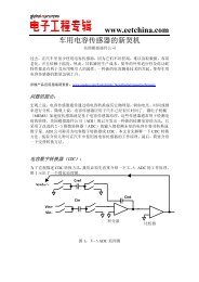
Figure 1. Discrete overvoltage protection circuitHow It WorksThe ma<strong>in</strong> pass element <strong>in</strong> the protection circuit shown <strong>in</strong> Figure 1 is the PNP transistor Q1.Care should be taken <strong>in</strong> select<strong>in</strong>g this part, as any power-supply voltage drops will bedeterm<strong>in</strong>ed by the characteristics of this transistor. A Zetex FMMT718 device has been usedfor this duty. The FFMT718 is one of a family of devices that exhibit very low VCE saturationvoltage values. This m<strong>in</strong>imizes the voltage drop <strong>in</strong>duced by the presence of the protectioncircuit. The transistor Q2 acts as the control element for Q1 and will turn on (turn<strong>in</strong>g Q1 off)when the voltage at the power-supply <strong>in</strong>put is equal to the sum of the zener voltage, due todiode D1 and Q2's own VBE voltage at a collector current of about 650uA. Q2 and D1 togetherproduce a typical trip voltage of 5.85V at 25°C. Approximately 0.53V of this is due to the VBEvoltage of Q2. The rema<strong>in</strong><strong>in</strong>g 5.32V is produced across D1. Note that the zener diode D1,although a nom<strong>in</strong>al 5.6V device, is be<strong>in</strong>g operated at a very low reverse current, about 200uAas def<strong>in</strong>ed by the VBE of Q2 together with the 2.7k resistor. At this current, the zener voltage isbelow the characteristic "knee" and is therefore less than the rated value. The 6.8k resistorconnected to the base of Q1 provides the current necessary to keep Q1 turned on under normalcircumstances.The circuit operates to disconnect the load dur<strong>in</strong>g overvoltage conditions. That is to say that Q1switches off when an overvoltage condition is detected, remov<strong>in</strong>g power from the load. Q1 willturn on aga<strong>in</strong> when the overvoltage condition is removed. One of the attractions of this type ofcircuit is <strong>in</strong> its response speed. The circuit <strong>in</strong> Figure 1 does not use feedback, so there are nohigh-order damp<strong>in</strong>g effects or slew-rate limitations to overcome. The full speed of theconstituent parts is available to prevent transient power-supply events from reach<strong>in</strong>g the load.Q2 has been chosen, for convenience, to be the same type as that chosen for Q1, although thereare no special requirements of this device and almost any PNP device could be substituted.www.maxim-ic.com/an760 Page 2 of 7
Reverse-Voltage <strong>Protection</strong>The circuit <strong>in</strong> Figure 1 will withstand reverse power-supply voltages of only about -5V. Thereverse breakdown voltages of the base emitter junctions Q1 and Q2 determ<strong>in</strong>e this figure.Additional circuitry is therefore required to provide the (-16V) reverse-voltage protectioncapability. Either one of two simple additions to the circuit <strong>in</strong> Figure 1 will provide thenecessary reverse-voltage protection. The first method employs a p-channel MOSFET, asshown <strong>in</strong> Figure 2. By configur<strong>in</strong>g the MOSFET as shown, the device's body diode willautomatically conduct when a power-supply voltage of greater than about 0.5V is present. Thebody diode of this transistor is a necessary feature, as without it the circuit would not start up.The addition of this component provides a disconnect function under reverse-voltageconditions. The only requirements for the reverse protection MOSFET are that it should be alow Ron, logic level type. A Si3441DV device is shown, but any similar device can besubstituted.Figure 2. P-channel MOSFET as the reverse-voltage protection elementCircuit PerformanceThe performance of the protection circuit <strong>in</strong> Figure 2 can be ascerta<strong>in</strong>ed from two pr<strong>in</strong>cipalmeasurements: trip voltage value and forward voltage drop. The graph <strong>in</strong> Figure 3 shows thetrip voltage versus the temperature characteristic for this circuit. The measurements for Figure3 were conducted us<strong>in</strong>g a sensor signal condition<strong>in</strong>g IC, the MAX1455, as the load circuit witha 1uF decoupl<strong>in</strong>g capacitor across the IC power-supply p<strong>in</strong>s. The nom<strong>in</strong>al current draw of theIC circuit dur<strong>in</strong>g the test was 3mA. Exam<strong>in</strong><strong>in</strong>g the plot <strong>in</strong> Figure 3, we can see that the tripvoltage of the protection circuit exhibits a temperature coefficient of -4mV/°C. Half of thisfigure is due to the VBE temperature characteristic of transistor Q2. The rema<strong>in</strong>der is producedwww.maxim-ic.com/an760 Page 3 of 7
y the zener diode D1. If a more accurate trip voltage value is required (one that has lessvariation with temperature), then a higher-perform<strong>in</strong>g voltage reference could be substituted forthe zener diode.Figure 3. Trip voltage versus temperature for the circuit <strong>in</strong> Figure 2The reverse-voltage protection characteristic of the circuit <strong>in</strong> Figure 2 can be characterized bythe reverse leakage measured over temperature with -16V applied to the power <strong>in</strong>put. Theresults obta<strong>in</strong>ed for reverse-leakage performance of the circuit <strong>in</strong> Figure 2 are shown <strong>in</strong> Table1, <strong>in</strong> which the reverse-leakage characteristic is presented as a leakage-resistance value.Table 1. Reverse-Leakage Resistance versus TemperatureTemperature(°C)Reverse-LeakageResistance (Ohms)-40 --5 -25 -60 -95 2.64E+12125 3.36E+11Note: The reverse-leakage current measured from -40°C to 60°C was effectively zero (<strong>in</strong>f<strong>in</strong>iteleakageresistance).www.maxim-ic.com/an760 Page 4 of 7
The forward voltage drop of the protection circuit <strong>in</strong> Figure 2 was measured at three supplyvoltages—4.5V, 5V, and 5.5V—for temperatures <strong>in</strong> the -40°C to 125°C range. The resultsobta<strong>in</strong>ed are presented <strong>in</strong> the graph <strong>in</strong> Figure 4.Figure 4. Forward voltage drop versus temperature for the circuit <strong>in</strong> Figure 2Exam<strong>in</strong><strong>in</strong>g the results <strong>in</strong> Figure 4 shows the forward voltage drop of the circuit <strong>in</strong> Figure 2 tobe below 6mV for temperatures <strong>in</strong> the -40°C to 125°C range. The effect of power-supplyvoltage drops on ratiometric measurement errors is the same as with any other system offsets,so long as the circuit has been calibrated with the protection circuit <strong>in</strong> place. When subjected toa 10% change <strong>in</strong> power-supply voltage, the error <strong>in</strong>duced by any offset with<strong>in</strong> the system willbe 10% of the offset value. So, a 6mV offset (voltage drop) will <strong>in</strong>duce a ratiometricmeasurement error of 0.6mV when the power supply is changed by 10%. In a system where theoutput span is set to 4V, this 0.6mV error will correspond to a measurement error of 0.015% ofspan.Less Expensive Reverse-Voltage <strong>Protection</strong>The circuit <strong>in</strong> Figure 2 uses a p-channel MOSFET as the reverse-voltage protection element.This has the advantage of disconnect<strong>in</strong>g the load dur<strong>in</strong>g reverse-voltage events and thereforeplaces no particular requirements on the power supply. A less expensive alternative to this is touse a simple diode connected across the power supply as the reverse protection element. Thisarrangement is shown <strong>in</strong> Figure 5, but can be used only where the ma<strong>in</strong> system power supply iscurrent-limited or fused. The diode protects the circuit by conduct<strong>in</strong>g whenever a reversevoltage is applied to the power-supply <strong>in</strong>puts of the circuit. The diode must be rated towithstand the maximum current or the fuse rat<strong>in</strong>g of the system's power source.www.maxim-ic.com/an760 Page 5 of 7
Figure 6. Fully protected, sensor signal conditioner circuit withstands the application of±16V to any wir<strong>in</strong>g connection.MORE INFORMATIONMAX1452: QuickView -- Full (PDF) Data Sheet (296k) -- Free SampleMAX1455: QuickView -- Full (PDF) Data Sheet (360k) -- Free SampleMAX1459: QuickView -- Full (PDF) Data Sheet (256k) -- Free SampleMAX1463: QuickView -- Full (PDF) Data Sheet (560k) -- Free SampleMAX1478: QuickView -- Full (PDF) Data Sheet (224k) -- Free Samplewww.maxim-ic.com/an760 Page 7 of 7