AN3216 Multilayer Chip Antenna
AN3216 Multilayer Chip Antenna
AN3216 Multilayer Chip Antenna

Create successful ePaper yourself
Turn your PDF publications into a flip-book with our unique Google optimized e-Paper software.
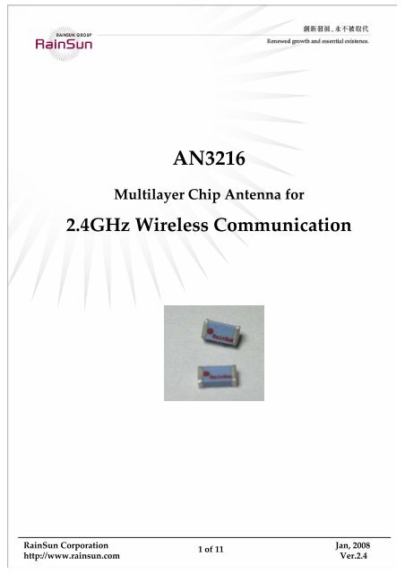
<strong>AN3216</strong><strong>Multilayer</strong> <strong>Chip</strong> <strong>Antenna</strong> for2.4GHz Wireless CommunicationRainSun Corporationhttp://www.rainsun.com1of 11Jan, 2008Ver.2.4
<strong>AN3216</strong> <strong>Multilayer</strong> <strong>Chip</strong> <strong>Antenna</strong>◆ Features• Light weight and low profile 3.2mm(L)X1.6mm(W)X1.04mm(H)• Omni‐directional in azimuth• Lead (Pb) Free◆ Applications• 2.4GHz wireless communications• 2.4GHz Modules• Bluetooth System• 802.11b/g Wireless LAN SystemSpecificationsCenter frequencyPeak gainOperation temperatureStorage temperatureVSWRInput ImpedancePower handlingBandwidthAzimuth beamwidthPolarizationSoldering pad2.45GHz0.5dBi (typ.)‐40 ~ +85 °C‐40 ~ +85 °C2.5 (Max)50 Ohm1W (Max)110MHz (typ.)Omni‐directionalLinearNatural tinRainSun Corporationhttp://www.rainsun.com2of 11Jan, 2008Ver.2.4
Pin configurationTop view12Pin No12Pin assignmentFeed terminationFeed point mark3Solder termination3DimensionsSymbolABCHDimensions(mm)3.20 ± 0.101.60 ± 0.100.30 ± 0.051.04 ± 0.20PCB Foot PrintSymbolDEFDimensions(mm)0.71.63.2RainSun Corporationhttp://www.rainsun.com3of 11Jan, 2008Ver.2.4
Recommended Test Board PatternTop viewBottom view50 OhmTransmission lineGround PlaneUnit : mmBoard thickness : 0.6mmBoard material : FR4SMA connectorFig-1Testing SetupMeasurementTesting Instrument:Anritsu 37369C VNA(Vector NetworkAnalyzer)VNA calibrate with 1 path reflectiononly calibration sequence on test boardfeed point.The test board dimension and it’slayout is the same as Fig‐1.RainSun Corporationhttp://www.rainsun.com4of 11Jan, 2008Ver.2.4
Typical Electrical CharacteristicsReturn lossSmith ChartMarker data:1 : f=2.411 GHz2 : f=2.450 GHz3 : f=2.492 GHzRainSun Corporationhttp://www.rainsun.com5of 11Jan, 2008Ver.2.4
Typical Radiation Patterns2.45 GHz H‐Planevertical2.45 GHz H‐Planehorizontal2.45 GHz E‐Planevertical2.45 GHz E‐PlanehorizontalRainSun Corporationhttp://www.rainsun.com6of 11Jan, 2008Ver.2.4
Typical Soldering Profile for Lead‐free ProcessTemperature ( °C )340°C300°C150°CPeak temp 340°C5 sec.25 sec.Pre-heatingDo not exceed 30 secs.Time (sec.)Reflow SolderingTemperature ( °C )260°C230°C180°C10 sec, max30 sec.60 sec.Pre-heatingTime (sec.)RainSun Corporationhttp://www.rainsun.com7of 11Jan, 2008Ver.2.4
Application exampleFig.2Best ChoiceAcceptableGround plane areaClearance area1. Placement of the antennaThe antenna shall be placed on a area without underlying ground plane at theedge of the PCB oriented as above. Ground plane area surrounding theantenna should be with minimum clearence 3mm.2. Placement of 2.4 GHz moduleTo avoid losses in the strip line, the module shall be placed as close to theantenna as possible.3. Strip lineThe strip line impendence must be dimensioned according to your specificPCB (see fig.2) to 50 Ohm. No crossing strip lines are allowed between thestrip line and its ground plane.4. Via Connections on PCBTo avoid spurious effects via connections must be made to analogue ground.Via connection depends on PCB layout design. Figure 2 for reference only.5. Component matchingComponent values are depending on antenna placement, PCB dimensionsand location of other components. PCB dimension and antenna location willeffect the antenna frequency.6. DC BlockIt might be needed depending on RF Module or chip hardware design.7. ClearanceNo components allowed within the clearence area with a minimum distanceto other components. The minimum distance is 3mm.RainSun Corporationhttp://www.rainsun.com8of 11Jan, 2008Ver.2.4
PackingBlister Tape SpecificationsSymbolWEFD 0D 1P 0P 1P 2A 0Dimension Tolerance Unit8.00 ± 0.10 mm1.75 ± 0.10 mm3.50 ± 0.05 mm1.55 ± 0.05 mm1.10 ± 0.10 mm4.00 ± 0.10 mm4.00 ± 0.10 mm2.00 ± 0.05 mm1.94 ± 0.10 mmB 03.53 ± 0.10 mm10 × P 0 40.00 ± 0.20 mmK 01.42 ± 0.05 mmT0.23 ± 0.01 mmT 2>0.05 ± 0.01 mmRainSun Corporationhttp://www.rainsun.com9of 11Jan, 2008Ver.2.4
Reel SpecificationsQuantityPer ReelTape Width(mm)A(mm)C(mm)B(mm)E(mm)W(mm)W 1(mm)3,0008178±113±0.260±0.52.2±0.59±0.512±0.05RainSun Corporationhttp://www.rainsun.com10 of 11Jan, 2008Ver.2.4
Tape SpecificationsTape Peel StrengthPeel‐off force should be in the range of 0.1~0.6 N at a peel‐off speed of 300 ±10 mm/min.Storage Conditions(1) Temperature : 15 to 35℃ , Relative Humidity (RH) : 45 to 75%.(2) Non-corrosive environment.RainSun Corporationhttp://www.rainsun.com11 of 11Jan, 2008Ver.2.4